WO2023037832A1 - 脈波センサ - Google Patents
脈波センサ Download PDFInfo
- Publication number
- WO2023037832A1 WO2023037832A1 PCT/JP2022/030969 JP2022030969W WO2023037832A1 WO 2023037832 A1 WO2023037832 A1 WO 2023037832A1 JP 2022030969 W JP2022030969 W JP 2022030969W WO 2023037832 A1 WO2023037832 A1 WO 2023037832A1
- Authority
- WO
- WIPO (PCT)
- Prior art keywords
- pulse wave
- strain
- resistor
- wave sensor
- metal layer
- Prior art date
- Legal status (The legal status is an assumption and is not a legal conclusion. Google has not performed a legal analysis and makes no representation as to the accuracy of the status listed.)
- Ceased
Links
Images



Classifications
-
- A—HUMAN NECESSITIES
- A61—MEDICAL OR VETERINARY SCIENCE; HYGIENE
- A61B—DIAGNOSIS; SURGERY; IDENTIFICATION
- A61B5/00—Measuring for diagnostic purposes; Identification of persons
- A61B5/02—Detecting, measuring or recording for evaluating the cardiovascular system, e.g. pulse, heart rate, blood pressure or blood flow
Definitions
- the present invention relates to pulse wave sensors.
- a pulse wave sensor that detects a pulse wave generated as the heart pumps out blood is known.
- a pulse wave sensor provided with a pressure-receiving plate serving as a strain-generating body supported flexibly by the action of an external force, and piezoelectric conversion means for converting the flexure of the pressure-receiving plate into an electric signal.
- the flexible area of the pressure receiving plate is formed in a dome shape with a convex curved surface facing outward, and a pressure detecting element is provided on the inner surface of the top of the pressure receiving plate as piezoelectric conversion means (for example, , see Patent Document 1).
- substantially fan-shaped through openings are radially arranged around the center position of the pressure receiving plate. Since the pulse wave sensor is a part that directly touches the subject's skin, foreign matter such as dust and water enters the pulse wave sensor through the through opening, causing electrical shorts and obstruction of flexibility due to foreign matter being caught. Problems can arise.
- the present invention has been made in view of the above points, and an object of the present invention is to provide a pulse wave sensor that prevents foreign matter from entering.
- the present pulse wave sensor has a strain body, and a strain gauge having a Cr mixed phase film as a resistor provided on the strain body, and the strain body includes a frame and a portion of the frame. and a connecting portion connecting the inner side of the frame and the outer side of the beam in a plan view without a gap, wherein the connecting portion is located between the frame and the beam. It is thin and detects a pulse wave based on the change in the resistance value of the resistor accompanying the deformation of the beam.
- FIG. 1 is a plan view illustrating a pulse wave sensor according to a first embodiment; FIG. It is a bottom view which illustrates the pulse wave sensor which concerns on 1st Embodiment.
- 1 is a cross-sectional view (part 1) illustrating a pulse wave sensor according to a first embodiment;
- FIG. 2 is a cross-sectional view (part 2) illustrating the pulse wave sensor according to the first embodiment;
- FIG. 4 is a cross-sectional view illustrating a housing to which a strain body is attached;
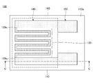
- 1 is a plan view illustrating a strain gauge according to a first embodiment;
- FIG. 1 is a cross-sectional view illustrating a strain gauge according to a first embodiment;
- FIG. 1 is a plan view illustrating the pulse wave sensor according to the first embodiment.
- FIG. FIG. 2 is a bottom view illustrating the pulse wave sensor according to the first embodiment;
- FIG. 3 is a cross-sectional view (Part 1) illustrating the pulse wave sensor according to the first embodiment, showing a cross section along line AA in FIG.
- FIG. 4 is a cross-sectional view (part 2) illustrating the pulse wave sensor according to the first embodiment, showing a cross section along line BB in FIG.
- a plan view is taken from the direction in which the load portion 14 projects, and a bottom view is taken from the direction in which the strain gauge 100 is provided.
- the pulse wave sensor 1 has a strain body 10 and a strain gauge 100.
- the pulse wave sensor 1 may have a shielded cable, a flexible substrate, or the like for inputting/outputting electrical signals to/from the outside.
- X, Y, Z indicate an orthogonal coordinate system.
- the strain body 10 has a frame portion 11, a beam portion 12, a connection portion 13, and a load portion 14. However, the load section 14 is provided as required.
- the strain-generating body 10 is, for example, a plate-like shape, and each constituent element is, for example, integrally formed.
- the strain-generating body 10 has, for example, a two-fold symmetrical shape in plan view.
- the strain-generating body 10 has, for example, a rectangular shape in plan view, but may have a circular or elliptical shape in plan view.
- the strain body 10 is rectangular in plan view, for example, the strain body 10 has two sides parallel to the X direction and two sides parallel to the Y direction.
- the outer diameter of the strain generating body 10 can be, for example, 20 ⁇ 2 mm (X direction) ⁇ 15 ⁇ 2 mm (Y direction).
- SUS stainless steel
- copper, aluminum, or the like can be used as a material of the strain generating body 10.
- the frame portion 11 is, for example, a rectangular frame-shaped region provided on the outermost side of the strain body 10 in plan view.
- the width W1 of the frame portion 11 is, for example, 1 mm or more and 5 mm or less.
- the width W1 of the frame portion 11 may or may not be constant.
- the beam portion 12 is provided so as to bridge the inside of the frame portion 11 .
- the beam portion 12 has, for example, a first beam 12a and a second beam 12b that intersect in a cross shape in plan view.
- a region where the first beam 12 a and the second beam 12 b intersect is a common portion of both and includes the center of the frame portion 11 .
- the first beam 12a which is one of the beams forming the cross
- the second beam 12b which is the other beam forming the cross
- the width W2 other than the crossing area is constant, and is, for example, 1 mm or more and 5 mm or less. Although it is not essential that the width W2 is constant, it is preferable to keep the width W2 constant in that strain can be detected linearly.
- the connecting portions 13 are four portions that connect the inner side of the frame portion 11 and the outer side of the beam portion 12 without gaps in plan view.
- the planar shape of each connection portion 13 is, for example, a rectangle.
- Each connecting portion 13 is thinner than the frame portion 11 and beam portion 12 .
- the thickness t1 of the frame portion 11 and the beam portion 12 is, for example, the same, and is, for example, 0.1 mm or more and 0.2 mm or less.
- the thickness t2 of the connecting portion 13 can be, for example, approximately half the thickness t1 .
- the load part 14 can be provided on the beam part 12 .
- the load portion 14 is provided, for example, in an area where the first beam 12a and the second beam 12b that constitute the beam portion 12 intersect.
- the load portion 14 protrudes from the upper surface of the beam portion 12 .
- the amount of protrusion of the load portion 14 with respect to the upper surface of the beam portion 12 is, for example, about 0.1 mm.
- the beam portion 12 is flexible, and elastically deforms when a load is applied to the load portion 14 .
- the strain gauge 100 is provided on the strain-generating body 10 .
- the strain gauge 100 can be provided on the lower surface side of the beam portion 12, for example. Since the beam portion 12 has a flat plate shape, the strain gauge can be easily attached.
- One or more strain gauges 100 may be provided, but four strain gauges 100 are provided in this embodiment. By providing four strain gauges 100, strain can be detected by a full bridge.
- Two of the four strain gauges 100 are arranged on the side near the frame portion 11 of the first beam 12a whose longitudinal direction is the X direction so as to face each other across the load portion 14 in a plan view.
- the other two of the four strain gauges 100 sandwich the load portion 14 in plan view on the side near the load portion 14 (the center side of the frame portion 11) of the second beam 12b whose longitudinal direction is the Y direction. are arranged to face each other.
- the pulse wave sensor 1 is used by being fixed to the subject's arm so that the load section 14 contacts the subject's radial artery.
- the resistance value of the resistor 130 (described later) of the strain gauge 100 changes.
- the pulse wave sensor 1 can detect a pulse wave based on the change in the resistance value of the resistor 130 of the strain gauge 100 accompanying the deformation of the beam portion 12 .
- a pulse wave is output as a periodic voltage change from a measuring circuit connected to an electrode 150 (described later) of the strain gauge 100, for example.
- Pulse wave detection accuracy can be improved.
- the length L1 of the first beam 12a and the length L2 of the second beam 12b may be the same, but the first beam 12a is preferably longer than the second beam 12b.
- the strain body 10 has a rectangular shape in plan view and the outer diameter of the strain body 10 is 20 mm (X direction) ⁇ 15 mm (Y direction)
- the length L 2 of the second beam 12b 13 mm.
- the pulse wave sensor 1 By fixing the pulse wave sensor 1 to the subject's arm so that the long first beam 12a is along the radial artery, the component along the radial artery can be acquired at a large signal level, so the S / N ratio is improved. It is possible to improve the detection accuracy of the pulse wave. Further, by fixing the pulse wave sensor 1 to the subject's arm so that the long first beam 12a is along the radial artery, it is preferable in that the low-frequency segment of the pulse wave can be obtained efficiently.
- the strain body 10 can be elliptical in plan view. Further, by making the strain generating body 10 circular in plan view and partially changing the width of the frame portion 11, it is possible to make the first beam 12a longer than the second beam 12b. However, making the strain-generating body 10 rectangular in plan view is more preferable than making the strain-generating body 10 in a circular or elliptical shape in plan view because it is easier to manufacture.
- the strain-generating body 10 may be attached to one side of the housing 20 as shown in FIG.
- the housing 20 is a portion that holds the strain body 10 .
- the housing 20 is, for example, in the shape of a box, closed on the bottom side and open on the top side.
- a rectangular strain-generating body 10 is fixed with an adhesive or the like so as to block the opening on the upper surface side of the housing 20 .
- the housing 20 can be made of metal, resin, or the like, for example. However, in order to prevent deterioration in strain detection accuracy due to the influence of thermal expansion, the strain body 10 and the housing 20 are preferably made of materials having the same coefficient of thermal expansion. For example, SUS (stainless steel) can be used as the material of the strain-generating body 10 and the housing 20 .
- one side in the thickness direction of the frame portion 11, the beam portion 12, and the connection portion 13 (the upper side in FIG. 3) is flush, and the load portion 14 is provided on one side. and strain gauges are provided on the other side opposite to the one side (lower side in FIG. 3).
- the flush sides of the frame portion 11, the beam portion 12, and the connection portion 13 are the sides that come into contact with the subject.
- the load section 14 may be provided on the other side (upper side in FIG. 3) and the strain gauge may be provided on one side (upper side in FIG. 3).
- the sides of the frame portion 11, the beam portion 12, and the connection portion 13 that are not flush with each other are the sides that come into contact with the subject.
- a structure in which the flush sides of the frame portion 11, the beam portion 12, and the connection portion 13 are the sides that contact the subject is preferable in that the subject is less likely to feel discomfort.
- the strain generating body 10 since the strain generating body 10 has the connection portion 13 that connects the inside of the frame portion 11 and the outside of the beam portion 12 without a gap in plan view, the pulse wave sensor There are no openings (gaps) for foreign matter to enter inside. Therefore, it is possible to prevent foreign matter such as dust and moisture from entering the pulse wave sensor 1, causing problems such as an electrical short circuit and a problem such as obstruction of flexibility due to the pinching of the foreign matter.
- the pulse wave sensor 1 can detect the pulse wave with high sensitivity based on the change in the resistance value of the resistor 130 accompanying the deformation of the beam portion 12 .
- the pulse wave sensor 1 has a highly sensitive strain gauge 100 with a gauge factor of 10 or more using a Cr mixed phase film described later as the resistor 130, so that the resistance of the resistor 130 accompanying deformation of the beam 12 A pulse wave can be detected with particularly high sensitivity based on changes in values.
- FIG. 6 is a plan view illustrating the strain gauge according to the first embodiment
- FIG. FIG. 7 is a cross-sectional view illustrating the strain gauge according to the first embodiment, showing a cross section along line CC of FIG. 6 and 7, the strain gauge 100 has a substrate 110, a resistor 130, wiring 140, electrodes 150, and a cover layer 160.
- the cover layer 160 may be provided as necessary.
- the side of the substrate 110 on which the resistor 130 is provided is the upper side or one side, and the resistor 130 is not provided. side is the bottom side or the other side.
- the surface on the side where the resistor 130 of each part is provided is defined as one surface or upper surface, and the surface on the side where the resistor 130 is not provided is defined as the other surface or the lower surface.
- the strain gauge 100 can be used upside down or placed at any angle. For example, in FIG. 5, the strain gauge 100 is affixed to the beam portion 12 in a state inverted from that in FIG. That is, the base material 110 in FIG. 7 is attached to the lower surface of the beam portion 12 with an adhesive or the like.
- planar view refers to viewing an object from the direction normal to the top surface 110a of the base material 110
- planar shape refers to the shape of the object viewed from the direction normal to the top surface 110a of the base material 110.
- the base material 110 is a member that serves as a base layer for forming the resistor 130 and the like, and has flexibility.
- the thickness of the base material 110 is not particularly limited, and can be appropriately selected according to the purpose. In particular, when the thickness of the base material 110 is 5 ⁇ m to 200 ⁇ m, the transmission of strain from the surface of the strain generating body bonded to the lower surface of the base material 110 via an adhesive layer or the like, and the dimensional stability against the environment.
- the thickness is preferably 10 ⁇ m or more, and more preferable from the viewpoint of insulation.
- the substrate 110 is made of, for example, PI (polyimide) resin, epoxy resin, PEEK (polyetheretherketone) resin, PEN (polyethylene naphthalate) resin, PET (polyethylene terephthalate) resin, PPS (polyphenylene sulfide) resin, LCP (liquid crystal It can be formed from an insulating resin film such as polymer) resin, polyolefin resin, or the like. Note that the film refers to a flexible member having a thickness of about 500 ⁇ m or less.
- the base material 110 may be formed from an insulating resin film containing a filler such as silica or alumina, for example.
- Materials other than the resin of the base material 110 include, for example, SiO 2 , ZrO 2 (including YSZ), Si, Si 2 N 3 , Al 2 O 3 (including sapphire), ZnO, perovskite ceramics (CaTiO 3 , BaTiO 3 ) and other crystalline materials, as well as amorphous glass and the like.
- a metal such as aluminum, an aluminum alloy (duralumin), or titanium may be used.
- an insulating film is formed on the base material 110 made of metal.
- the resistor 130 is a thin film formed in a predetermined pattern on the base material 110, and is a sensing part that undergoes a change in resistance when subjected to strain.
- the resistor 130 may be formed directly on the upper surface 110a of the base material 110, or may be formed on the upper surface 110a of the base material 110 via another layer.
- the resistor 130 is shown with a dark pear-skin pattern for the sake of convenience.
- a plurality of elongated portions are arranged in the same longitudinal direction (the direction of line CC in FIG. 6) at predetermined intervals, and the ends of adjacent elongated portions are alternately connected. , is a zigzag folding structure as a whole.
- the longitudinal direction of the elongated portions is the grid direction, and the direction perpendicular to the grid direction is the grid width direction (the direction perpendicular to line CC in FIG. 6).
- One ends in the longitudinal direction of the two elongated portions located on the outermost side in the grid width direction are bent in the grid width direction to form respective ends 130e 1 and 130e 2 of the resistor 130 in the grid width direction.
- Each end 130 e 1 and 130 e 2 of the resistor 130 in the grid width direction is electrically connected to the electrode 150 via the wiring 140 .
- the wiring 140 electrically connects the ends 130e 1 and 130e 2 of the resistor 130 in the grid width direction and each electrode 150 .
- the resistor 130 can be made of, for example, a material containing Cr (chromium), a material containing Ni (nickel), or a material containing both Cr and Ni. That is, the resistor 130 can be made of a material containing at least one of Cr and Ni.
- Materials containing Cr include, for example, a Cr mixed phase film.
- Materials containing Ni include, for example, Cu—Ni (copper nickel).
- Materials containing both Cr and Ni include, for example, Ni—Cr (nickel chromium).
- the Cr mixed phase film is a film in which Cr, CrN, Cr 2 N, or the like is mixed.
- the Cr mixed phase film may contain unavoidable impurities such as chromium oxide.
- the thickness of the resistor 130 is not particularly limited, and can be appropriately selected according to the purpose.
- the crystallinity of the crystal for example, the crystallinity of ⁇ -Cr
- the thickness of the resistor 130 is 1 ⁇ m or less in that cracks in the film caused by internal stress of the film constituting the resistor 130 and warping from the base material 110 can be reduced.
- the width of the resistor 130 can be optimized with respect to the required specifications such as the resistance value and the lateral sensitivity, and can be set to, for example, about 10 ⁇ m to 100 ⁇ m in consideration of disconnection countermeasures.
- the stability of gauge characteristics can be improved by using ⁇ -Cr (alpha chromium), which is a stable crystal phase, as the main component.
- the gauge factor of the strain gauge 100 is 10 or more, and the temperature coefficient of gauge factor TCS and the temperature coefficient of resistance TCR are in the range of -1000 ppm/°C to +1000 ppm/°C.
- the term "main component" means that the target material accounts for 50% by weight or more of all the materials constituting the resistor. It preferably contains 90% by weight or more, more preferably 90% by weight or more.
- ⁇ -Cr is Cr with a bcc structure (body-centered cubic lattice structure).
- the resistor 130 is a Cr mixed phase film
- CrN and Cr 2 N contained in the Cr mixed phase film be 20% by weight or less.
- CrN and Cr 2 N contained in the Cr mixed phase film are 20% by weight or less, a decrease in gauge factor can be suppressed.
- the ratio of Cr 2 N in CrN and Cr 2 N is preferably 80% by weight or more and less than 90% by weight, more preferably 90% by weight or more and less than 95% by weight.
- the ratio of Cr 2 N in CrN and Cr 2 N is 90% by weight or more and less than 95% by weight, the decrease in TCR (negative TCR) becomes more pronounced due to Cr 2 N having semiconducting properties. .
- by reducing ceramicization brittle fracture is reduced.
- the wiring 140 is formed on the base material 110 and electrically connected to the resistor 130 and the electrode 150 .
- the wiring 140 has a first metal layer 141 and a second metal layer 142 laminated on the upper surface of the first metal layer 141 .
- the wiring 140 is not limited to a straight line, and may have any pattern. Also, the wiring 140 can be of any width and any length. In FIG. 6, the wiring 140 and the electrode 150 are shown with a satin pattern that is thinner than the resistor 130 for the sake of convenience.
- the electrode 150 is formed on the base material 110 and electrically connected to the resistor 130 via the wiring 140.
- the electrode 150 is wider than the wiring 140 and formed in a substantially rectangular shape.
- the electrodes 150 are a pair of electrodes for outputting to the outside the change in the resistance value of the resistor 130 caused by strain, and are connected to, for example, lead wires for external connection.
- the electrode 150 has a pair of first metal layers 151 and a second metal layer 152 laminated on the upper surface of each first metal layer 151 .
- the first metal layer 151 is electrically connected to the ends 130e 1 and 130e 2 of the resistor 130 via the first metal layer 141 of the wiring 140 .
- the first metal layer 151 is formed in a substantially rectangular shape in plan view.
- the first metal layer 151 may be formed to have the same width as the wiring 140 .
- the resistor 130, the first metal layer 141, and the first metal layer 151 are denoted by different symbols for convenience, they can be integrally formed from the same material in the same process. Therefore, the resistor 130, the first metal layer 141, and the first metal layer 151 have substantially the same thickness.
- the second metal layer 142 and the second metal layer 152 are given different symbols for the sake of convenience, they can be integrally formed from the same material in the same process. Therefore, the second metal layer 142 and the second metal layer 152 have substantially the same thickness.
- the second metal layers 142 and 152 are made of a material with lower resistance than the resistor 130 (the first metal layers 141 and 151).
- the materials for the second metal layers 142 and 152 are not particularly limited as long as they have lower resistance than the resistor 130, and can be appropriately selected according to the purpose.
- the material of the second metal layers 142 and 152 is Cu, Ni, Al, Ag, Au, Pt, etc., or an alloy of any of these metals, or any of these. or a laminated film obtained by appropriately laminating any of these metals, alloys, or compounds.
- the thickness of the second metal layers 142 and 152 is not particularly limited and can be appropriately selected according to the purpose, but can be, for example, about 3 ⁇ m to 5 ⁇ m.
- the second metal layers 142 and 152 may be formed on part of the top surfaces of the first metal layers 141 and 151 or may be formed on the entire top surfaces of the first metal layers 141 and 151 .
- One or more other metal layers may be laminated on the upper surface of the second metal layer 152 .
- a copper layer may be used as the second metal layer 152, and a gold layer may be laminated on the upper surface of the copper layer.
- a copper layer may be used as the second metal layer 152, and a palladium layer and a gold layer may be sequentially laminated on the upper surface of the copper layer. Solder wettability of the electrode 150 can be improved by using a gold layer as the top layer of the electrode 150 .
- the wiring 140 has a structure in which the second metal layer 142 is laminated on the first metal layer 141 made of the same material as the resistor 130 . Therefore, since the wiring 140 has a lower resistance than the resistor 130, the wiring 140 can be prevented from functioning as a resistor. As a result, the accuracy of strain detection by the resistor 130 can be improved.
- the wiring 140 having a resistance lower than that of the resistor 130 it is possible to limit the substantial sensing portion of the strain gauge 100 to the local area where the resistor 130 is formed. Therefore, the strain detection accuracy by the resistor 130 can be improved.
- the wiring 140 has a lower resistance than the resistor 130, and the resistor 130 is formed as a substantial sensing part. Restricting to a local region exhibits a significant effect in improving strain detection accuracy. Further, making the wiring 140 lower in resistance than the resistor 130 also has the effect of reducing lateral sensitivity.
- a cover layer 160 is formed on the base material 110 to cover the resistors 130 and the wirings 140 and expose the electrodes 150 .
- a portion of the wiring 140 may be exposed from the cover layer 160 .
- the cover layer 160 can be made of insulating resin such as PI resin, epoxy resin, PEEK resin, PEN resin, PET resin, PPS resin, composite resin (eg, silicone resin, polyolefin resin).
- the cover layer 160 may contain fillers and pigments.
- the thickness of the cover layer 160 is not particularly limited, and can be appropriately selected according to the purpose.
- the base material 110 is prepared, and a metal layer (referred to as metal layer A for convenience) is formed on the upper surface 110a of the base material 110.
- the metal layer A is a layer that is finally patterned to become the resistor 130 , the first metal layer 141 and the first metal layer 151 . Therefore, the material and thickness of the metal layer A are the same as those of the resistor 130, the first metal layer 141, and the first metal layer 151 described above.
- the metal layer A can be formed, for example, by magnetron sputtering using a raw material capable of forming the metal layer A as a target.
- the metal layer A may be formed by using a reactive sputtering method, a vapor deposition method, an arc ion plating method, a pulse laser deposition method, or the like instead of the magnetron sputtering method.
- a functional layer having a predetermined thickness is vacuum-formed on the upper surface 110a of the base material 110 as a base layer by conventional sputtering, for example. is preferred.
- a functional layer refers to a layer having a function of promoting crystal growth of at least the upper metal layer A (resistor 130).
- the functional layer preferably further has a function of preventing oxidation of the metal layer A due to oxygen and moisture contained in the base material 110 and a function of improving adhesion between the base material 110 and the metal layer A.
- the functional layer may also have other functions.
- the insulating resin film that constitutes the base material 110 contains oxygen and moisture, especially when the metal layer A contains Cr, Cr forms a self-oxidizing film. Being prepared helps.
- the material of the functional layer is not particularly limited as long as it has a function of promoting the crystal growth of at least the upper metal layer A (resistor 130), and can be appropriately selected according to the purpose. Chromium), Ti (titanium), V (vanadium), Nb (niobium), Ta (tantalum), Ni (nickel), Y (yttrium), Zr (zirconium), Hf (hafnium), Si (silicon), C ( carbon), Zn (zinc), Cu (copper), Bi (bismuth), Fe (iron), Mo (molybdenum), W (tungsten), Ru (ruthenium), Rh (rhodium), Re (rhenium), Os ( osmium), Ir (iridium), Pt (platinum), Pd (palladium), Ag (silver), Au (gold), Co (cobalt), Mn (manganese), Al (aluminum) 1 selected from the group consisting of Metal or metals, alloys of any of this group of
- Examples of the above alloy include FeCr, TiAl, FeNi, NiCr, CrCu, and the like.
- Examples of the above compounds include TiN, TaN , Si3N4 , TiO2 , Ta2O5 , SiO2 and the like.
- the thickness of the functional layer is preferably 1/20 or less of the thickness of the resistor. Within this range, it is possible to promote the crystal growth of ⁇ -Cr, and to prevent a part of the current flowing through the resistor from flowing through the functional layer, thereby preventing a decrease in strain detection sensitivity.
- the thickness of the functional layer is more preferably 1/50 or less of the thickness of the resistor. Within this range, it is possible to promote the crystal growth of ⁇ -Cr, and further prevent the deterioration of the strain detection sensitivity due to part of the current flowing through the resistor flowing through the functional layer.
- the thickness of the functional layer is more preferably 1/100 or less of the thickness of the resistor. Within such a range, it is possible to further prevent a decrease in strain detection sensitivity due to part of the current flowing through the resistor flowing through the functional layer.
- the film thickness of the functional layer is preferably 1 nm to 1 ⁇ m. Within such a range, the crystal growth of ⁇ -Cr can be promoted, and the film can be easily formed without causing cracks in the functional layer.
- the thickness of the functional layer is more preferably 1 nm to 0.8 ⁇ m. Within such a range, the crystal growth of ⁇ -Cr can be promoted, and the functional layer can be formed more easily without cracks.
- the thickness of the functional layer is more preferably 1 nm to 0.5 ⁇ m. Within such a range, the crystal growth of ⁇ -Cr can be promoted, and the functional layer can be formed more easily without cracks.
- planar shape of the functional layer is patterned to be substantially the same as the planar shape of the resistor shown in FIG. 6, for example.
- the planar shape of the functional layer is not limited to being substantially the same as the planar shape of the resistor. If the functional layer is made of an insulating material, it may not be patterned in the same planar shape as the resistor. In this case, the functional layer may be solidly formed at least in the region where the resistor is formed. Alternatively, the functional layer may be formed all over the top surface of the substrate 110 .
- the thickness and surface area of the functional layer can be increased by forming the functional layer relatively thick such that the thickness is 50 nm or more and 1 ⁇ m or less and forming the functional layer in a solid manner. Since the resistance increases, the heat generated by the resistor can be dissipated to the base material 110 side. As a result, in the strain gauge 100, deterioration in measurement accuracy due to self-heating of the resistor can be suppressed.
- the functional layer can be formed, for example, by conventional sputtering using a raw material capable of forming the functional layer as a target and introducing Ar (argon) gas into the chamber in a vacuum.
- Ar argon
- the functional layer is formed while etching the upper surface 110a of the substrate 110 with Ar, so that the amount of film formation of the functional layer can be minimized and the effect of improving adhesion can be obtained.
- the functional layer may be formed by other methods.
- the upper surface 110a of the substrate 110 is activated by a plasma treatment using Ar or the like to obtain an adhesion improvement effect, and then the functional layer is vacuum-formed by magnetron sputtering. You may use the method to do.
- the combination of the material of the functional layer and the material of the metal layer A is not particularly limited and can be appropriately selected according to the purpose. It is possible to form a Cr mixed phase film as a main component.
- the metal layer A can be formed by magnetron sputtering using a raw material capable of forming a Cr mixed-phase film as a target and introducing Ar gas into the chamber.
- the metal layer A may be formed by reactive sputtering using pure Cr as a target, introducing an appropriate amount of nitrogen gas into the chamber together with Ar gas.
- the introduction amount and pressure (nitrogen partial pressure) of nitrogen gas and adjusting the heating temperature by providing a heating process by changing the introduction amount and pressure (nitrogen partial pressure) of nitrogen gas and adjusting the heating temperature by providing a heating process, the ratio of CrN and Cr 2 N contained in the Cr mixed phase film, and the ratio of CrN and Cr The proportion of Cr2N in 2N can be adjusted.
- the growth surface of the Cr mixed phase film is defined by the functional layer made of Ti, and a Cr mixed phase film whose main component is ⁇ -Cr, which has a stable crystal structure, can be formed.
- the diffusion of Ti constituting the functional layer into the Cr mixed phase film improves the gauge characteristics.
- the strain gauge 100 can have a gauge factor of 10 or more and a temperature coefficient of gauge factor TCS and a temperature coefficient of resistance TCR within the range of -1000 ppm/°C to +1000 ppm/°C.
- the Cr mixed phase film may contain Ti or TiN (titanium nitride).
- the functional layer made of Ti has the function of promoting the crystal growth of the metal layer A and the function of preventing oxidation of the metal layer A due to oxygen and moisture contained in the base material 110. , and the function of improving the adhesion between the base material 110 and the metal layer A.
- Ta, Si, Al, or Fe is used as the functional layer instead of Ti.
- the functional layer below the metal layer A in this manner, it is possible to promote the crystal growth of the metal layer A, and the metal layer A having a stable crystal phase can be produced. As a result, in the strain gauge 100, the stability of gauge characteristics can be improved. In addition, by diffusing the material forming the functional layer into the metal layer A, the gauge characteristics of the strain gauge 100 can be improved.
- a second metal layer 142 and a second metal layer 152 are formed on the upper surface of the metal layer A.
- the second metal layer 142 and the second metal layer 152 can be formed by photolithography, for example.
- a seed layer is formed so as to cover the upper surface of the metal layer A by, for example, sputtering or electroless plating.
- a photosensitive resist is formed on the entire upper surface of the seed layer, exposed and developed to form openings exposing regions where the second metal layers 142 and 152 are to be formed.
- the pattern of the second metal layer 142 can be made into an arbitrary shape by adjusting the shape of the opening of the resist.
- the resist for example, a dry film resist or the like can be used.
- a second metal layer 142 and a second metal layer 152 are formed on the seed layer exposed in the opening, for example, by electroplating using the seed layer as a power supply path.
- the electroplating method is suitable in that the tact time is high and low-stress electroplating layers can be formed as the second metal layer 142 and the second metal layer 152 .
- the strain gauge 100 can be prevented from warping by reducing the stress of the thick electroplated layer.
- the second metal layer 142 and the second metal layer 152 may be formed by electroless plating.
- the resist can be removed, for example, by immersing it in a solution capable of dissolving the material of the resist.
- a photosensitive resist is formed on the entire upper surface of the seed layer, exposed and developed, and patterned into a planar shape similar to the resistor 130, wiring 140, and electrode 150 in FIG.
- the resist for example, a dry film resist or the like can be used.
- the metal layer A and the seed layer exposed from the resist are removed to form the planar resistor 130, the wiring 140 and the electrode 150 shown in FIG.
- wet etching can remove unnecessary portions of the metal layer A and the seed layer.
- the functional layer is patterned by etching into the planar shape shown in FIG. At this point, a seed layer is formed on the resistor 130, the first metal layer 141, and the first metal layer 151. Next, as shown in FIG.
- the unnecessary seed layer can be removed by wet etching using an etchant that etches the seed layer but does not etch the functional layer, resistor 130 , wiring 140 , and electrode 150 .
- the strain gauge 100 is completed by providing a cover layer 160 that covers the resistor 130 and the wiring 140 and exposes the electrodes 150 on the upper surface 110a of the base material 110, if necessary.
- a cover layer 160 for example, a semi-cured thermosetting insulating resin film is laminated on the upper surface 110a of the base material 110 so as to cover the resistor 130 and the wiring 140 and expose the electrodes 150, and is cured by heating.
- the cover layer 160 is formed by coating the upper surface 110a of the base material 110 with a liquid or paste thermosetting insulating resin so as to cover the resistor 130 and the wiring 140 and expose the electrodes 150, and heat and harden the resin. may be made.
- Reference Signs List 1 pulse wave sensor 10 strain generating body, 11 frame, 12 beam, 12a first beam, 12b second beam, 13 connection portion, 14 load portion, 20 housing, 100 strain gauge, 110 base material, 110a upper surface , 130 resistor, 130e 1 , 130e 2 termination, 140 wiring, 150 electrode, 160 cover layer
Landscapes
- Health & Medical Sciences (AREA)
- Life Sciences & Earth Sciences (AREA)
- Biomedical Technology (AREA)
- Molecular Biology (AREA)
- Physiology (AREA)
- Biophysics (AREA)
- Pathology (AREA)
- Engineering & Computer Science (AREA)
- Cardiology (AREA)
- Heart & Thoracic Surgery (AREA)
- Medical Informatics (AREA)
- Physics & Mathematics (AREA)
- Surgery (AREA)
- Animal Behavior & Ethology (AREA)
- General Health & Medical Sciences (AREA)
- Public Health (AREA)
- Veterinary Medicine (AREA)
- Measuring Pulse, Heart Rate, Blood Pressure Or Blood Flow (AREA)
- Measurement Of Length, Angles, Or The Like Using Electric Or Magnetic Means (AREA)
Applications Claiming Priority (2)
| Application Number | Priority Date | Filing Date | Title |
|---|---|---|---|
| JP2021146128A JP7571976B2 (ja) | 2021-09-08 | 2021-09-08 | 脈波センサ |
| JP2021-146128 | 2021-09-08 |
Publications (1)
| Publication Number | Publication Date |
|---|---|
| WO2023037832A1 true WO2023037832A1 (ja) | 2023-03-16 |
Family
ID=85507581
Family Applications (1)
| Application Number | Title | Priority Date | Filing Date |
|---|---|---|---|
| PCT/JP2022/030969 Ceased WO2023037832A1 (ja) | 2021-09-08 | 2022-08-16 | 脈波センサ |
Country Status (2)
| Country | Link |
|---|---|
| JP (1) | JP7571976B2 (https=) |
| WO (1) | WO2023037832A1 (https=) |
Families Citing this family (1)
| Publication number | Priority date | Publication date | Assignee | Title |
|---|---|---|---|---|
| JP2025021156A (ja) * | 2023-07-31 | 2025-02-13 | ミネベアミツミ株式会社 | 脈波測定装置 |
Citations (6)
| Publication number | Priority date | Publication date | Assignee | Title |
|---|---|---|---|---|
| JPS5983023A (ja) * | 1982-11-04 | 1984-05-14 | Hitachi Ltd | 半導体圧力差圧検出器 |
| JPS62176430A (ja) * | 1985-09-17 | 1987-08-03 | セントロン ベー.フェー. | カテ−テル端圧力変換器 |
| JPH05340957A (ja) * | 1992-06-08 | 1993-12-24 | Fujikura Ltd | 半導体センサの製造方法および半導体センサ |
| JPH11183515A (ja) * | 1997-12-25 | 1999-07-09 | Matsushita Electric Ind Co Ltd | 加速度センサ |
| JP2016063936A (ja) * | 2014-09-24 | 2016-04-28 | 株式会社アドバンテスト | 脈波センサユニット |
| US20160146685A1 (en) * | 2014-11-25 | 2016-05-26 | Continental Automotive Systems, Inc. | Piezoresistive pressure sensor device |
-
2021
- 2021-09-08 JP JP2021146128A patent/JP7571976B2/ja active Active
-
2022
- 2022-08-16 WO PCT/JP2022/030969 patent/WO2023037832A1/ja not_active Ceased
Patent Citations (6)
| Publication number | Priority date | Publication date | Assignee | Title |
|---|---|---|---|---|
| JPS5983023A (ja) * | 1982-11-04 | 1984-05-14 | Hitachi Ltd | 半導体圧力差圧検出器 |
| JPS62176430A (ja) * | 1985-09-17 | 1987-08-03 | セントロン ベー.フェー. | カテ−テル端圧力変換器 |
| JPH05340957A (ja) * | 1992-06-08 | 1993-12-24 | Fujikura Ltd | 半導体センサの製造方法および半導体センサ |
| JPH11183515A (ja) * | 1997-12-25 | 1999-07-09 | Matsushita Electric Ind Co Ltd | 加速度センサ |
| JP2016063936A (ja) * | 2014-09-24 | 2016-04-28 | 株式会社アドバンテスト | 脈波センサユニット |
| US20160146685A1 (en) * | 2014-11-25 | 2016-05-26 | Continental Automotive Systems, Inc. | Piezoresistive pressure sensor device |
Also Published As
| Publication number | Publication date |
|---|---|
| JP2023039125A (ja) | 2023-03-20 |
| JP7571976B2 (ja) | 2024-10-23 |
Similar Documents
| Publication | Publication Date | Title |
|---|---|---|
| JP7570975B2 (ja) | ひずみゲージ | |
| US20240230433A1 (en) | Pulse wave sensor | |
| WO2021205981A1 (ja) | ひずみゲージ | |
| WO2023037832A1 (ja) | 脈波センサ | |
| US20230375325A1 (en) | Strain gauge | |
| JP7537836B2 (ja) | バイタルセンサ | |
| JP7623065B2 (ja) | 脈波測定装置 | |
| WO2022259703A1 (ja) | ひずみゲージ | |
| JP2022008026A (ja) | ひずみゲージ | |
| JP7845619B2 (ja) | 脈波測定装置 | |
| JP2022093237A (ja) | ひずみゲージ | |
| US12329504B2 (en) | Vital sensor | |
| JP7658050B2 (ja) | ひずみゲージ、センサモジュール、及び起歪体 | |
| US20250228464A1 (en) | Pulse wave sensor | |
| JP7652502B2 (ja) | センサモジュール、電池パック | |
| US12595998B2 (en) | Strain gauge | |
| US20250155306A1 (en) | Pulse wave sensor | |
| JP2023021714A (ja) | 脈波測定装置 | |
| WO2024190692A1 (ja) | 脈波センサ | |
| JP2024117474A (ja) | 押圧力センサ | |
| JP2023037918A (ja) | ひずみゲージ | |
| JP2023129273A (ja) | 脈波センサ | |
| JP2022075113A (ja) | ひずみゲージ | |
| JP2022188394A (ja) | ひずみゲージ、ロードセル |
Legal Events
| Date | Code | Title | Description |
|---|---|---|---|
| 121 | Ep: the epo has been informed by wipo that ep was designated in this application |
Ref document number: 22867154 Country of ref document: EP Kind code of ref document: A1 |
|
| NENP | Non-entry into the national phase |
Ref country code: DE |
|
| 122 | Ep: pct application non-entry in european phase |
Ref document number: 22867154 Country of ref document: EP Kind code of ref document: A1 |