WO2023037198A1 - 表示装置 - Google Patents
表示装置 Download PDFInfo
- Publication number
- WO2023037198A1 WO2023037198A1 PCT/IB2022/057991 IB2022057991W WO2023037198A1 WO 2023037198 A1 WO2023037198 A1 WO 2023037198A1 IB 2022057991 W IB2022057991 W IB 2022057991W WO 2023037198 A1 WO2023037198 A1 WO 2023037198A1
- Authority
- WO
- WIPO (PCT)
- Prior art keywords
- layer
- insulating layer
- light
- insulating
- pixel electrode
- Prior art date
Links
- 229920005989 resin Polymers 0.000 claims description 59
- 239000011347 resin Substances 0.000 claims description 59
- 238000009413 insulation Methods 0.000 abstract 8
- 239000010410 layer Substances 0.000 description 2159
- 239000010408 film Substances 0.000 description 367
- 238000000034 method Methods 0.000 description 173
- 238000005401 electroluminescence Methods 0.000 description 171
- 230000006870 function Effects 0.000 description 161
- 239000000463 material Substances 0.000 description 146
- 239000000758 substrate Substances 0.000 description 115
- 239000004065 semiconductor Substances 0.000 description 91
- 238000002347 injection Methods 0.000 description 59
- 239000007924 injection Substances 0.000 description 59
- 238000004519 manufacturing process Methods 0.000 description 43
- 239000000126 substance Substances 0.000 description 43
- 239000011701 zinc Substances 0.000 description 42
- 239000011241 protective layer Substances 0.000 description 41
- 238000005530 etching Methods 0.000 description 36
- 229910052751 metal Inorganic materials 0.000 description 35
- 230000015572 biosynthetic process Effects 0.000 description 34
- 239000002184 metal Substances 0.000 description 34
- 238000012545 processing Methods 0.000 description 34
- QVGXLLKOCUKJST-UHFFFAOYSA-N atomic oxygen Chemical compound [O] QVGXLLKOCUKJST-UHFFFAOYSA-N 0.000 description 30
- 239000001301 oxygen Substances 0.000 description 30
- 229910052760 oxygen Inorganic materials 0.000 description 30
- 229910052782 aluminium Inorganic materials 0.000 description 28
- XAGFODPZIPBFFR-UHFFFAOYSA-N aluminium Chemical compound [Al] XAGFODPZIPBFFR-UHFFFAOYSA-N 0.000 description 27
- 230000003287 optical effect Effects 0.000 description 25
- XLYOFNOQVPJJNP-UHFFFAOYSA-N water Substances O XLYOFNOQVPJJNP-UHFFFAOYSA-N 0.000 description 25
- PXHVJJICTQNCMI-UHFFFAOYSA-N Nickel Chemical compound [Ni] PXHVJJICTQNCMI-UHFFFAOYSA-N 0.000 description 24
- 239000003086 colorant Substances 0.000 description 24
- 239000010949 copper Substances 0.000 description 24
- 238000000231 atomic layer deposition Methods 0.000 description 23
- 230000005525 hole transport Effects 0.000 description 23
- TWNQGVIAIRXVLR-UHFFFAOYSA-N oxo(oxoalumanyloxy)alumane Chemical compound O=[Al]O[Al]=O TWNQGVIAIRXVLR-UHFFFAOYSA-N 0.000 description 23
- XUIMIQQOPSSXEZ-UHFFFAOYSA-N Silicon Chemical compound [Si] XUIMIQQOPSSXEZ-UHFFFAOYSA-N 0.000 description 22
- 229910052710 silicon Inorganic materials 0.000 description 22
- 239000010703 silicon Substances 0.000 description 22
- 239000007789 gas Substances 0.000 description 21
- 239000000203 mixture Substances 0.000 description 21
- 230000032258 transport Effects 0.000 description 21
- RYGMFSIKBFXOCR-UHFFFAOYSA-N Copper Chemical compound [Cu] RYGMFSIKBFXOCR-UHFFFAOYSA-N 0.000 description 20
- 239000003990 capacitor Substances 0.000 description 20
- 229910052802 copper Inorganic materials 0.000 description 20
- 239000012535 impurity Substances 0.000 description 20
- 150000004767 nitrides Chemical class 0.000 description 20
- 238000004891 communication Methods 0.000 description 18
- 230000006378 damage Effects 0.000 description 18
- 230000008569 process Effects 0.000 description 17
- 229910052581 Si3N4 Inorganic materials 0.000 description 16
- 239000000956 alloy Substances 0.000 description 16
- 238000001312 dry etching Methods 0.000 description 16
- 238000003384 imaging method Methods 0.000 description 16
- HQVNEWCFYHHQES-UHFFFAOYSA-N silicon nitride Chemical compound N12[Si]34N5[Si]62N3[Si]51N64 HQVNEWCFYHHQES-UHFFFAOYSA-N 0.000 description 16
- 238000004544 sputter deposition Methods 0.000 description 16
- 239000010936 titanium Substances 0.000 description 16
- XEEYBQQBJWHFJM-UHFFFAOYSA-N Iron Chemical compound [Fe] XEEYBQQBJWHFJM-UHFFFAOYSA-N 0.000 description 15
- KDLHZDBZIXYQEI-UHFFFAOYSA-N Palladium Chemical compound [Pd] KDLHZDBZIXYQEI-UHFFFAOYSA-N 0.000 description 15
- VYPSYNLAJGMNEJ-UHFFFAOYSA-N Silicium dioxide Chemical compound O=[Si]=O VYPSYNLAJGMNEJ-UHFFFAOYSA-N 0.000 description 15
- 229910045601 alloy Inorganic materials 0.000 description 15
- 229910052738 indium Inorganic materials 0.000 description 15
- APFVFJFRJDLVQX-UHFFFAOYSA-N indium atom Chemical compound [In] APFVFJFRJDLVQX-UHFFFAOYSA-N 0.000 description 15
- 229910044991 metal oxide Inorganic materials 0.000 description 15
- 150000004706 metal oxides Chemical class 0.000 description 15
- 238000001039 wet etching Methods 0.000 description 15
- GYHNNYVSQQEPJS-UHFFFAOYSA-N Gallium Chemical compound [Ga] GYHNNYVSQQEPJS-UHFFFAOYSA-N 0.000 description 14
- 230000004888 barrier function Effects 0.000 description 14
- -1 copper-magnesium-aluminum Chemical compound 0.000 description 14
- 229910052733 gallium Inorganic materials 0.000 description 14
- 229910052719 titanium Inorganic materials 0.000 description 14
- 229910052721 tungsten Inorganic materials 0.000 description 14
- RTAQQCXQSZGOHL-UHFFFAOYSA-N Titanium Chemical compound [Ti] RTAQQCXQSZGOHL-UHFFFAOYSA-N 0.000 description 13
- 239000010937 tungsten Substances 0.000 description 13
- IJGRMHOSHXDMSA-UHFFFAOYSA-N Atomic nitrogen Chemical compound N#N IJGRMHOSHXDMSA-UHFFFAOYSA-N 0.000 description 12
- 238000000576 coating method Methods 0.000 description 12
- 239000011368 organic material Substances 0.000 description 12
- 229910052814 silicon oxide Inorganic materials 0.000 description 12
- WFKWXMTUELFFGS-UHFFFAOYSA-N tungsten Chemical compound [W] WFKWXMTUELFFGS-UHFFFAOYSA-N 0.000 description 12
- 238000007740 vapor deposition Methods 0.000 description 12
- 229920000178 Acrylic resin Polymers 0.000 description 11
- 239000004925 Acrylic resin Substances 0.000 description 11
- 238000006243 chemical reaction Methods 0.000 description 11
- 238000005229 chemical vapour deposition Methods 0.000 description 11
- 230000000694 effects Effects 0.000 description 11
- 238000010438 heat treatment Methods 0.000 description 11
- 239000007769 metal material Substances 0.000 description 11
- 229910052750 molybdenum Inorganic materials 0.000 description 11
- 229910052759 nickel Inorganic materials 0.000 description 11
- BASFCYQUMIYNBI-UHFFFAOYSA-N platinum Chemical compound [Pt] BASFCYQUMIYNBI-UHFFFAOYSA-N 0.000 description 11
- 229910052727 yttrium Inorganic materials 0.000 description 11
- ZOKXTWBITQBERF-UHFFFAOYSA-N Molybdenum Chemical compound [Mo] ZOKXTWBITQBERF-UHFFFAOYSA-N 0.000 description 10
- 239000004793 Polystyrene Substances 0.000 description 10
- ATJFFYVFTNAWJD-UHFFFAOYSA-N Tin Chemical compound [Sn] ATJFFYVFTNAWJD-UHFFFAOYSA-N 0.000 description 10
- XLOMVQKBTHCTTD-UHFFFAOYSA-N Zinc monoxide Chemical compound [Zn]=O XLOMVQKBTHCTTD-UHFFFAOYSA-N 0.000 description 10
- 229910052796 boron Inorganic materials 0.000 description 10
- 238000010586 diagram Methods 0.000 description 10
- 239000011159 matrix material Substances 0.000 description 10
- 239000011733 molybdenum Substances 0.000 description 10
- 150000002894 organic compounds Chemical class 0.000 description 10
- 239000002356 single layer Substances 0.000 description 10
- 239000010409 thin film Substances 0.000 description 10
- 229910052718 tin Inorganic materials 0.000 description 10
- BQCADISMDOOEFD-UHFFFAOYSA-N Silver Chemical compound [Ag] BQCADISMDOOEFD-UHFFFAOYSA-N 0.000 description 9
- 239000012790 adhesive layer Substances 0.000 description 9
- 229910052709 silver Inorganic materials 0.000 description 9
- 239000004332 silver Substances 0.000 description 9
- VWQVUPCCIRVNHF-UHFFFAOYSA-N yttrium atom Chemical compound [Y] VWQVUPCCIRVNHF-UHFFFAOYSA-N 0.000 description 9
- FYYHWMGAXLPEAU-UHFFFAOYSA-N Magnesium Chemical compound [Mg] FYYHWMGAXLPEAU-UHFFFAOYSA-N 0.000 description 8
- 239000000853 adhesive Substances 0.000 description 8
- 230000001070 adhesive effect Effects 0.000 description 8
- 238000001514 detection method Methods 0.000 description 8
- 238000009792 diffusion process Methods 0.000 description 8
- 239000010931 gold Substances 0.000 description 8
- 239000011777 magnesium Substances 0.000 description 8
- 230000001681 protective effect Effects 0.000 description 8
- WGTYBPLFGIVFAS-UHFFFAOYSA-M tetramethylammonium hydroxide Chemical compound [OH-].C[N+](C)(C)C WGTYBPLFGIVFAS-UHFFFAOYSA-M 0.000 description 8
- UFHFLCQGNIYNRP-UHFFFAOYSA-N Hydrogen Chemical compound [H][H] UFHFLCQGNIYNRP-UHFFFAOYSA-N 0.000 description 7
- HCHKCACWOHOZIP-UHFFFAOYSA-N Zinc Chemical compound [Zn] HCHKCACWOHOZIP-UHFFFAOYSA-N 0.000 description 7
- 239000011651 chromium Substances 0.000 description 7
- 150000001875 compounds Chemical class 0.000 description 7
- 239000004020 conductor Substances 0.000 description 7
- 230000006866 deterioration Effects 0.000 description 7
- 238000011161 development Methods 0.000 description 7
- 230000018109 developmental process Effects 0.000 description 7
- 239000001257 hydrogen Substances 0.000 description 7
- 229910052739 hydrogen Inorganic materials 0.000 description 7
- 239000011810 insulating material Substances 0.000 description 7
- 229910052742 iron Inorganic materials 0.000 description 7
- 229910052749 magnesium Inorganic materials 0.000 description 7
- 230000007246 mechanism Effects 0.000 description 7
- 229910052715 tantalum Inorganic materials 0.000 description 7
- 238000012546 transfer Methods 0.000 description 7
- 238000001771 vacuum deposition Methods 0.000 description 7
- 229910052725 zinc Inorganic materials 0.000 description 7
- KFZMGEQAYNKOFK-UHFFFAOYSA-N Isopropanol Chemical compound CC(C)O KFZMGEQAYNKOFK-UHFFFAOYSA-N 0.000 description 6
- 229910052779 Neodymium Inorganic materials 0.000 description 6
- NBIIXXVUZAFLBC-UHFFFAOYSA-N Phosphoric acid Chemical compound OP(O)(O)=O NBIIXXVUZAFLBC-UHFFFAOYSA-N 0.000 description 6
- 239000012298 atmosphere Substances 0.000 description 6
- 229910052804 chromium Inorganic materials 0.000 description 6
- 239000011248 coating agent Substances 0.000 description 6
- 239000011521 glass Substances 0.000 description 6
- PCHJSUWPFVWCPO-UHFFFAOYSA-N gold Chemical compound [Au] PCHJSUWPFVWCPO-UHFFFAOYSA-N 0.000 description 6
- 229910052737 gold Inorganic materials 0.000 description 6
- 229910000449 hafnium oxide Inorganic materials 0.000 description 6
- WIHZLLGSGQNAGK-UHFFFAOYSA-N hafnium(4+);oxygen(2-) Chemical compound [O-2].[O-2].[Hf+4] WIHZLLGSGQNAGK-UHFFFAOYSA-N 0.000 description 6
- AMGQUBHHOARCQH-UHFFFAOYSA-N indium;oxotin Chemical compound [In].[Sn]=O AMGQUBHHOARCQH-UHFFFAOYSA-N 0.000 description 6
- 229910010272 inorganic material Inorganic materials 0.000 description 6
- MRELNEQAGSRDBK-UHFFFAOYSA-N lanthanum(3+);oxygen(2-) Chemical compound [O-2].[O-2].[O-2].[La+3].[La+3] MRELNEQAGSRDBK-UHFFFAOYSA-N 0.000 description 6
- QEFYFXOXNSNQGX-UHFFFAOYSA-N neodymium atom Chemical compound [Nd] QEFYFXOXNSNQGX-UHFFFAOYSA-N 0.000 description 6
- PLDDOISOJJCEMH-UHFFFAOYSA-N neodymium(3+);oxygen(2-) Chemical compound [O-2].[O-2].[O-2].[Nd+3].[Nd+3] PLDDOISOJJCEMH-UHFFFAOYSA-N 0.000 description 6
- 229910052757 nitrogen Inorganic materials 0.000 description 6
- 229910052756 noble gas Inorganic materials 0.000 description 6
- 229910052763 palladium Inorganic materials 0.000 description 6
- 238000000206 photolithography Methods 0.000 description 6
- 229920006122 polyamide resin Polymers 0.000 description 6
- 229910021420 polycrystalline silicon Inorganic materials 0.000 description 6
- 229920001721 polyimide Polymers 0.000 description 6
- 238000007639 printing Methods 0.000 description 6
- 239000002904 solvent Substances 0.000 description 6
- 238000004528 spin coating Methods 0.000 description 6
- GUVRBAGPIYLISA-UHFFFAOYSA-N tantalum atom Chemical compound [Ta] GUVRBAGPIYLISA-UHFFFAOYSA-N 0.000 description 6
- VYZAMTAEIAYCRO-UHFFFAOYSA-N Chromium Chemical compound [Cr] VYZAMTAEIAYCRO-UHFFFAOYSA-N 0.000 description 5
- LFQSCWFLJHTTHZ-UHFFFAOYSA-N Ethanol Chemical compound CCO LFQSCWFLJHTTHZ-UHFFFAOYSA-N 0.000 description 5
- QCWXUUIWCKQGHC-UHFFFAOYSA-N Zirconium Chemical compound [Zr] QCWXUUIWCKQGHC-UHFFFAOYSA-N 0.000 description 5
- 230000000903 blocking effect Effects 0.000 description 5
- 229910017052 cobalt Inorganic materials 0.000 description 5
- 239000010941 cobalt Substances 0.000 description 5
- GUTLYIVDDKVIGB-UHFFFAOYSA-N cobalt atom Chemical compound [Co] GUTLYIVDDKVIGB-UHFFFAOYSA-N 0.000 description 5
- PMHQVHHXPFUNSP-UHFFFAOYSA-M copper(1+);methylsulfanylmethane;bromide Chemical compound Br[Cu].CSC PMHQVHHXPFUNSP-UHFFFAOYSA-M 0.000 description 5
- 238000000151 deposition Methods 0.000 description 5
- 239000003822 epoxy resin Substances 0.000 description 5
- 235000019441 ethanol Nutrition 0.000 description 5
- 210000001508 eye Anatomy 0.000 description 5
- 238000005247 gettering Methods 0.000 description 5
- 229910052746 lanthanum Inorganic materials 0.000 description 5
- FZLIPJUXYLNCLC-UHFFFAOYSA-N lanthanum atom Chemical compound [La] FZLIPJUXYLNCLC-UHFFFAOYSA-N 0.000 description 5
- 239000002346 layers by function Substances 0.000 description 5
- 239000007788 liquid Substances 0.000 description 5
- 238000004768 lowest unoccupied molecular orbital Methods 0.000 description 5
- 229910052697 platinum Inorganic materials 0.000 description 5
- 229920000647 polyepoxide Polymers 0.000 description 5
- 239000009719 polyimide resin Substances 0.000 description 5
- 238000007789 sealing Methods 0.000 description 5
- 239000011787 zinc oxide Substances 0.000 description 5
- 229910052726 zirconium Inorganic materials 0.000 description 5
- 229910000838 Al alloy Inorganic materials 0.000 description 4
- ZOXJGFHDIHLPTG-UHFFFAOYSA-N Boron Chemical group [B] ZOXJGFHDIHLPTG-UHFFFAOYSA-N 0.000 description 4
- OKTJSMMVPCPJKN-UHFFFAOYSA-N Carbon Chemical compound [C] OKTJSMMVPCPJKN-UHFFFAOYSA-N 0.000 description 4
- WHXSMMKQMYFTQS-UHFFFAOYSA-N Lithium Chemical compound [Li] WHXSMMKQMYFTQS-UHFFFAOYSA-N 0.000 description 4
- 239000004372 Polyvinyl alcohol Substances 0.000 description 4
- NRTOMJZYCJJWKI-UHFFFAOYSA-N Titanium nitride Chemical compound [Ti]#N NRTOMJZYCJJWKI-UHFFFAOYSA-N 0.000 description 4
- 238000010521 absorption reaction Methods 0.000 description 4
- 229910021417 amorphous silicon Inorganic materials 0.000 description 4
- XJHCXCQVJFPJIK-UHFFFAOYSA-M caesium fluoride Chemical compound [F-].[Cs+] XJHCXCQVJFPJIK-UHFFFAOYSA-M 0.000 description 4
- 230000008859 change Effects 0.000 description 4
- 230000000295 complement effect Effects 0.000 description 4
- 230000008021 deposition Effects 0.000 description 4
- 239000000428 dust Substances 0.000 description 4
- 230000001747 exhibiting effect Effects 0.000 description 4
- 230000005669 field effect Effects 0.000 description 4
- 229910052732 germanium Inorganic materials 0.000 description 4
- GNPVGFCGXDBREM-UHFFFAOYSA-N germanium atom Chemical compound [Ge] GNPVGFCGXDBREM-UHFFFAOYSA-N 0.000 description 4
- 229910052735 hafnium Inorganic materials 0.000 description 4
- VBJZVLUMGGDVMO-UHFFFAOYSA-N hafnium atom Chemical compound [Hf] VBJZVLUMGGDVMO-UHFFFAOYSA-N 0.000 description 4
- 210000003128 head Anatomy 0.000 description 4
- 239000011147 inorganic material Substances 0.000 description 4
- 229910052744 lithium Inorganic materials 0.000 description 4
- 239000005011 phenolic resin Substances 0.000 description 4
- 238000000623 plasma-assisted chemical vapour deposition Methods 0.000 description 4
- 229920002037 poly(vinyl butyral) polymer Polymers 0.000 description 4
- 229920002451 polyvinyl alcohol Polymers 0.000 description 4
- 239000000047 product Substances 0.000 description 4
- 238000004549 pulsed laser deposition Methods 0.000 description 4
- 239000000243 solution Substances 0.000 description 4
- JBQYATWDVHIOAR-UHFFFAOYSA-N tellanylidenegermanium Chemical compound [Te]=[Ge] JBQYATWDVHIOAR-UHFFFAOYSA-N 0.000 description 4
- 238000002834 transmittance Methods 0.000 description 4
- XESMNQMWRSEIET-UHFFFAOYSA-N 2,9-dinaphthalen-2-yl-4,7-diphenyl-1,10-phenanthroline Chemical compound C1=CC=CC=C1C1=CC(C=2C=C3C=CC=CC3=CC=2)=NC2=C1C=CC1=C(C=3C=CC=CC=3)C=C(C=3C=C4C=CC=CC4=CC=3)N=C21 XESMNQMWRSEIET-UHFFFAOYSA-N 0.000 description 3
- DHDHJYNTEFLIHY-UHFFFAOYSA-N 4,7-diphenyl-1,10-phenanthroline Chemical compound C1=CC=CC=C1C1=CC=NC2=C1C=CC1=C(C=3C=CC=CC=3)C=CN=C21 DHDHJYNTEFLIHY-UHFFFAOYSA-N 0.000 description 3
- QTBSBXVTEAMEQO-UHFFFAOYSA-N Acetic acid Chemical compound CC(O)=O QTBSBXVTEAMEQO-UHFFFAOYSA-N 0.000 description 3
- 229910052684 Cerium Inorganic materials 0.000 description 3
- 229910001111 Fine metal Inorganic materials 0.000 description 3
- OKKJLVBELUTLKV-UHFFFAOYSA-N Methanol Chemical compound OC OKKJLVBELUTLKV-UHFFFAOYSA-N 0.000 description 3
- MUBZPKHOEPUJKR-UHFFFAOYSA-N Oxalic acid Chemical compound OC(=O)C(O)=O MUBZPKHOEPUJKR-UHFFFAOYSA-N 0.000 description 3
- 229910052769 Ytterbium Inorganic materials 0.000 description 3
- 230000001133 acceleration Effects 0.000 description 3
- 229910000147 aluminium phosphate Inorganic materials 0.000 description 3
- GPBUGPUPKAGMDK-UHFFFAOYSA-N azanylidynemolybdenum Chemical compound [Mo]#N GPBUGPUPKAGMDK-UHFFFAOYSA-N 0.000 description 3
- UMIVXZPTRXBADB-UHFFFAOYSA-N benzocyclobutene Chemical compound C1=CC=C2CCC2=C1 UMIVXZPTRXBADB-UHFFFAOYSA-N 0.000 description 3
- 229910052790 beryllium Inorganic materials 0.000 description 3
- ATBAMAFKBVZNFJ-UHFFFAOYSA-N beryllium atom Chemical group [Be] ATBAMAFKBVZNFJ-UHFFFAOYSA-N 0.000 description 3
- 239000001913 cellulose Substances 0.000 description 3
- 229920002678 cellulose Polymers 0.000 description 3
- ZMIGMASIKSOYAM-UHFFFAOYSA-N cerium Chemical group [Ce][Ce][Ce][Ce][Ce][Ce][Ce][Ce][Ce][Ce][Ce][Ce][Ce][Ce][Ce][Ce][Ce][Ce][Ce][Ce][Ce][Ce][Ce][Ce][Ce][Ce][Ce][Ce][Ce][Ce][Ce][Ce][Ce][Ce][Ce][Ce][Ce][Ce] ZMIGMASIKSOYAM-UHFFFAOYSA-N 0.000 description 3
- 239000002131 composite material Substances 0.000 description 3
- 230000007797 corrosion Effects 0.000 description 3
- 238000005260 corrosion Methods 0.000 description 3
- 238000007766 curtain coating Methods 0.000 description 3
- 238000013461 design Methods 0.000 description 3
- AJNVQOSZGJRYEI-UHFFFAOYSA-N digallium;oxygen(2-) Chemical compound [O-2].[O-2].[O-2].[Ga+3].[Ga+3] AJNVQOSZGJRYEI-UHFFFAOYSA-N 0.000 description 3
- 238000007598 dipping method Methods 0.000 description 3
- KPUWHANPEXNPJT-UHFFFAOYSA-N disiloxane Chemical class [SiH3]O[SiH3] KPUWHANPEXNPJT-UHFFFAOYSA-N 0.000 description 3
- 238000010894 electron beam technology Methods 0.000 description 3
- 238000001704 evaporation Methods 0.000 description 3
- 229910001195 gallium oxide Inorganic materials 0.000 description 3
- 238000004770 highest occupied molecular orbital Methods 0.000 description 3
- 238000007654 immersion Methods 0.000 description 3
- 229910003437 indium oxide Inorganic materials 0.000 description 3
- PJXISJQVUVHSOJ-UHFFFAOYSA-N indium(iii) oxide Chemical compound [O-2].[O-2].[O-2].[In+3].[In+3] PJXISJQVUVHSOJ-UHFFFAOYSA-N 0.000 description 3
- PQXKHYXIUOZZFA-UHFFFAOYSA-M lithium fluoride Chemical compound [Li+].[F-] PQXKHYXIUOZZFA-UHFFFAOYSA-M 0.000 description 3
- 239000011572 manganese Substances 0.000 description 3
- 229910021421 monocrystalline silicon Inorganic materials 0.000 description 3
- 238000007645 offset printing Methods 0.000 description 3
- 230000003647 oxidation Effects 0.000 description 3
- 238000007254 oxidation reaction Methods 0.000 description 3
- SIWVEOZUMHYXCS-UHFFFAOYSA-N oxo(oxoyttriooxy)yttrium Chemical compound O=[Y]O[Y]=O SIWVEOZUMHYXCS-UHFFFAOYSA-N 0.000 description 3
- BPUBBGLMJRNUCC-UHFFFAOYSA-N oxygen(2-);tantalum(5+) Chemical compound [O-2].[O-2].[O-2].[O-2].[O-2].[Ta+5].[Ta+5] BPUBBGLMJRNUCC-UHFFFAOYSA-N 0.000 description 3
- RVTZCBVAJQQJTK-UHFFFAOYSA-N oxygen(2-);zirconium(4+) Chemical compound [O-2].[O-2].[Zr+4] RVTZCBVAJQQJTK-UHFFFAOYSA-N 0.000 description 3
- 229920002120 photoresistant polymer Polymers 0.000 description 3
- 239000004800 polyvinyl chloride Substances 0.000 description 3
- 229920000915 polyvinyl chloride Polymers 0.000 description 3
- 239000002243 precursor Substances 0.000 description 3
- 238000003672 processing method Methods 0.000 description 3
- 239000002096 quantum dot Substances 0.000 description 3
- 238000007650 screen-printing Methods 0.000 description 3
- 238000005507 spraying Methods 0.000 description 3
- 229910001936 tantalum oxide Inorganic materials 0.000 description 3
- 238000010345 tape casting Methods 0.000 description 3
- 229910052720 vanadium Inorganic materials 0.000 description 3
- GPPXJZIENCGNKB-UHFFFAOYSA-N vanadium Chemical group [V]#[V] GPPXJZIENCGNKB-UHFFFAOYSA-N 0.000 description 3
- NAWDYIZEMPQZHO-UHFFFAOYSA-N ytterbium Chemical compound [Yb] NAWDYIZEMPQZHO-UHFFFAOYSA-N 0.000 description 3
- 229910001928 zirconium oxide Inorganic materials 0.000 description 3
- 229910001316 Ag alloy Inorganic materials 0.000 description 2
- XKRFYHLGVUSROY-UHFFFAOYSA-N Argon Chemical compound [Ar] XKRFYHLGVUSROY-UHFFFAOYSA-N 0.000 description 2
- 229920002284 Cellulose triacetate Polymers 0.000 description 2
- 229920000089 Cyclic olefin copolymer Polymers 0.000 description 2
- MYMOFIZGZYHOMD-UHFFFAOYSA-N Dioxygen Chemical compound O=O MYMOFIZGZYHOMD-UHFFFAOYSA-N 0.000 description 2
- KRHYYFGTRYWZRS-UHFFFAOYSA-N Fluorane Chemical compound F KRHYYFGTRYWZRS-UHFFFAOYSA-N 0.000 description 2
- PEDCQBHIVMGVHV-UHFFFAOYSA-N Glycerine Chemical compound OCC(O)CO PEDCQBHIVMGVHV-UHFFFAOYSA-N 0.000 description 2
- PWHULOQIROXLJO-UHFFFAOYSA-N Manganese Chemical compound [Mn] PWHULOQIROXLJO-UHFFFAOYSA-N 0.000 description 2
- 229910000861 Mg alloy Inorganic materials 0.000 description 2
- 239000002202 Polyethylene glycol Substances 0.000 description 2
- 239000004373 Pullulan Substances 0.000 description 2
- 229920001218 Pullulan Polymers 0.000 description 2
- JUJWROOIHBZHMG-UHFFFAOYSA-N Pyridine Chemical group C1=CC=NC=C1 JUJWROOIHBZHMG-UHFFFAOYSA-N 0.000 description 2
- SMWDFEZZVXVKRB-UHFFFAOYSA-N Quinoline Chemical compound N1=CC=CC2=CC=CC=C21 SMWDFEZZVXVKRB-UHFFFAOYSA-N 0.000 description 2
- NNLVGZFZQQXQNW-ADJNRHBOSA-N [(2r,3r,4s,5r,6s)-4,5-diacetyloxy-3-[(2s,3r,4s,5r,6r)-3,4,5-triacetyloxy-6-(acetyloxymethyl)oxan-2-yl]oxy-6-[(2r,3r,4s,5r,6s)-4,5,6-triacetyloxy-2-(acetyloxymethyl)oxan-3-yl]oxyoxan-2-yl]methyl acetate Chemical compound O([C@@H]1O[C@@H]([C@H]([C@H](OC(C)=O)[C@H]1OC(C)=O)O[C@H]1[C@@H]([C@@H](OC(C)=O)[C@H](OC(C)=O)[C@@H](COC(C)=O)O1)OC(C)=O)COC(=O)C)[C@@H]1[C@@H](COC(C)=O)O[C@@H](OC(C)=O)[C@H](OC(C)=O)[C@H]1OC(C)=O NNLVGZFZQQXQNW-ADJNRHBOSA-N 0.000 description 2
- 229910052783 alkali metal Inorganic materials 0.000 description 2
- 150000001340 alkali metals Chemical class 0.000 description 2
- 229910052784 alkaline earth metal Inorganic materials 0.000 description 2
- 150000001342 alkaline earth metals Chemical class 0.000 description 2
- 239000007864 aqueous solution Substances 0.000 description 2
- 229910052786 argon Inorganic materials 0.000 description 2
- 150000004982 aromatic amines Chemical class 0.000 description 2
- WZJYKHNJTSNBHV-UHFFFAOYSA-N benzo[h]quinoline Chemical class C1=CN=C2C3=CC=CC=C3C=CC2=C1 WZJYKHNJTSNBHV-UHFFFAOYSA-N 0.000 description 2
- DQXBYHZEEUGOBF-UHFFFAOYSA-N but-3-enoic acid;ethene Chemical compound C=C.OC(=O)CC=C DQXBYHZEEUGOBF-UHFFFAOYSA-N 0.000 description 2
- 229910052792 caesium Inorganic materials 0.000 description 2
- TVFDJXOCXUVLDH-UHFFFAOYSA-N caesium atom Chemical compound [Cs] TVFDJXOCXUVLDH-UHFFFAOYSA-N 0.000 description 2
- 239000011575 calcium Substances 0.000 description 2
- 150000001716 carbazoles Chemical class 0.000 description 2
- 229910052799 carbon Inorganic materials 0.000 description 2
- 239000000969 carrier Substances 0.000 description 2
- 238000012937 correction Methods 0.000 description 2
- 238000002484 cyclic voltammetry Methods 0.000 description 2
- 230000002950 deficient Effects 0.000 description 2
- 230000003111 delayed effect Effects 0.000 description 2
- 229910001882 dioxygen Inorganic materials 0.000 description 2
- 238000006073 displacement reaction Methods 0.000 description 2
- 238000001035 drying Methods 0.000 description 2
- 230000005684 electric field Effects 0.000 description 2
- 239000005038 ethylene vinyl acetate Substances 0.000 description 2
- 230000005281 excited state Effects 0.000 description 2
- 210000000744 eyelid Anatomy 0.000 description 2
- YBMRDBCBODYGJE-UHFFFAOYSA-N germanium oxide Inorganic materials O=[Ge]=O YBMRDBCBODYGJE-UHFFFAOYSA-N 0.000 description 2
- 230000009477 glass transition Effects 0.000 description 2
- 229910021389 graphene Inorganic materials 0.000 description 2
- LNEPOXFFQSENCJ-UHFFFAOYSA-N haloperidol Chemical compound C1CC(O)(C=2C=CC(Cl)=CC=2)CCN1CCCC(=O)C1=CC=C(F)C=C1 LNEPOXFFQSENCJ-UHFFFAOYSA-N 0.000 description 2
- 150000002390 heteroarenes Chemical class 0.000 description 2
- 150000003949 imides Chemical class 0.000 description 2
- 239000011261 inert gas Substances 0.000 description 2
- 150000002484 inorganic compounds Chemical class 0.000 description 2
- 229910052741 iridium Inorganic materials 0.000 description 2
- GKOZUEZYRPOHIO-UHFFFAOYSA-N iridium atom Chemical class [Ir] GKOZUEZYRPOHIO-UHFFFAOYSA-N 0.000 description 2
- 238000002955 isolation Methods 0.000 description 2
- 239000003446 ligand Substances 0.000 description 2
- 239000004973 liquid crystal related substance Substances 0.000 description 2
- 239000000395 magnesium oxide Substances 0.000 description 2
- CPLXHLVBOLITMK-UHFFFAOYSA-N magnesium oxide Inorganic materials [Mg]=O CPLXHLVBOLITMK-UHFFFAOYSA-N 0.000 description 2
- AXZKOIWUVFPNLO-UHFFFAOYSA-N magnesium;oxygen(2-) Chemical compound [O-2].[Mg+2] AXZKOIWUVFPNLO-UHFFFAOYSA-N 0.000 description 2
- 230000005389 magnetism Effects 0.000 description 2
- 229910052748 manganese Inorganic materials 0.000 description 2
- 238000005259 measurement Methods 0.000 description 2
- 238000002844 melting Methods 0.000 description 2
- 230000008018 melting Effects 0.000 description 2
- 150000002739 metals Chemical class 0.000 description 2
- 238000002156 mixing Methods 0.000 description 2
- 150000002835 noble gases Chemical class 0.000 description 2
- 239000003960 organic solvent Substances 0.000 description 2
- 125000002524 organometallic group Chemical group 0.000 description 2
- PVADDRMAFCOOPC-UHFFFAOYSA-N oxogermanium Chemical compound [Ge]=O PVADDRMAFCOOPC-UHFFFAOYSA-N 0.000 description 2
- 230000035699 permeability Effects 0.000 description 2
- 229920001568 phenolic resin Polymers 0.000 description 2
- 238000005240 physical vapour deposition Methods 0.000 description 2
- 229920001200 poly(ethylene-vinyl acetate) Polymers 0.000 description 2
- 239000004417 polycarbonate Substances 0.000 description 2
- 229920000515 polycarbonate Polymers 0.000 description 2
- 229920001223 polyethylene glycol Polymers 0.000 description 2
- 229920000139 polyethylene terephthalate Polymers 0.000 description 2
- 239000005020 polyethylene terephthalate Substances 0.000 description 2
- 229920005591 polysilicon Polymers 0.000 description 2
- 229920001343 polytetrafluoroethylene Polymers 0.000 description 2
- 239000004810 polytetrafluoroethylene Substances 0.000 description 2
- 229920000036 polyvinylpyrrolidone Polymers 0.000 description 2
- 239000001267 polyvinylpyrrolidone Substances 0.000 description 2
- 235000013855 polyvinylpyrrolidone Nutrition 0.000 description 2
- 235000019423 pullulan Nutrition 0.000 description 2
- 125000003373 pyrazinyl group Chemical group 0.000 description 2
- 150000003222 pyridines Chemical class 0.000 description 2
- 229940083082 pyrimidine derivative acting on arteriolar smooth muscle Drugs 0.000 description 2
- 150000003230 pyrimidines Chemical class 0.000 description 2
- 125000000714 pyrimidinyl group Chemical group 0.000 description 2
- 150000003252 quinoxalines Chemical class 0.000 description 2
- 230000005855 radiation Effects 0.000 description 2
- 229910052761 rare earth metal Inorganic materials 0.000 description 2
- 150000002910 rare earth metals Chemical class 0.000 description 2
- 238000006748 scratching Methods 0.000 description 2
- 230000002393 scratching effect Effects 0.000 description 2
- 229920002050 silicone resin Polymers 0.000 description 2
- 239000007787 solid Substances 0.000 description 2
- 239000007921 spray Substances 0.000 description 2
- 238000003860 storage Methods 0.000 description 2
- 238000002230 thermal chemical vapour deposition Methods 0.000 description 2
- YVTHLONGBIQYBO-UHFFFAOYSA-N zinc indium(3+) oxygen(2-) Chemical compound [O--].[Zn++].[In+3] YVTHLONGBIQYBO-UHFFFAOYSA-N 0.000 description 2
- JYEUMXHLPRZUAT-UHFFFAOYSA-N 1,2,3-triazine Chemical group C1=CN=NN=C1 JYEUMXHLPRZUAT-UHFFFAOYSA-N 0.000 description 1
- QWENRTYMTSOGBR-UHFFFAOYSA-N 1H-1,2,3-Triazole Chemical group C=1C=NNN=1 QWENRTYMTSOGBR-UHFFFAOYSA-N 0.000 description 1
- KXGFMDJXCMQABM-UHFFFAOYSA-N 2-methoxy-6-methylphenol Chemical compound [CH]OC1=CC=CC([CH])=C1O KXGFMDJXCMQABM-UHFFFAOYSA-N 0.000 description 1
- AEJARLYXNFRVLK-UHFFFAOYSA-N 4H-1,2,3-triazole Chemical group C1C=NN=N1 AEJARLYXNFRVLK-UHFFFAOYSA-N 0.000 description 1
- JWBHNEZMQMERHA-UHFFFAOYSA-N 5,6,11,12,17,18-hexaazatrinaphthylene Chemical compound C1=CC=C2N=C3C4=NC5=CC=CC=C5N=C4C4=NC5=CC=CC=C5N=C4C3=NC2=C1 JWBHNEZMQMERHA-UHFFFAOYSA-N 0.000 description 1
- 229910018137 Al-Zn Inorganic materials 0.000 description 1
- 229910018573 Al—Zn Inorganic materials 0.000 description 1
- ROFVEXUMMXZLPA-UHFFFAOYSA-N Bipyridyl Chemical class N1=CC=CC=C1C1=CC=CC=N1 ROFVEXUMMXZLPA-UHFFFAOYSA-N 0.000 description 1
- OYPRJOBELJOOCE-UHFFFAOYSA-N Calcium Chemical compound [Ca] OYPRJOBELJOOCE-UHFFFAOYSA-N 0.000 description 1
- 229910000881 Cu alloy Inorganic materials 0.000 description 1
- 235000002673 Dioscorea communis Nutrition 0.000 description 1
- 241000544230 Dioscorea communis Species 0.000 description 1
- 229910052693 Europium Inorganic materials 0.000 description 1
- 229910012294 LiPP Inorganic materials 0.000 description 1
- GRYLNZFGIOXLOG-UHFFFAOYSA-N Nitric acid Chemical compound O[N+]([O-])=O GRYLNZFGIOXLOG-UHFFFAOYSA-N 0.000 description 1
- 239000004677 Nylon Substances 0.000 description 1
- 229910001252 Pd alloy Inorganic materials 0.000 description 1
- 229910002668 Pd-Cu Inorganic materials 0.000 description 1
- 208000035753 Periorbital contusion Diseases 0.000 description 1
- OAICVXFJPJFONN-UHFFFAOYSA-N Phosphorus Chemical compound [P] OAICVXFJPJFONN-UHFFFAOYSA-N 0.000 description 1
- 229920012266 Poly(ether sulfone) PES Polymers 0.000 description 1
- 239000004962 Polyamide-imide Substances 0.000 description 1
- 239000004642 Polyimide Substances 0.000 description 1
- 239000004743 Polypropylene Substances 0.000 description 1
- 229920001328 Polyvinylidene chloride Polymers 0.000 description 1
- 229910008355 Si-Sn Inorganic materials 0.000 description 1
- 229910006453 Si—Sn Inorganic materials 0.000 description 1
- 229910020994 Sn-Zn Inorganic materials 0.000 description 1
- 229910009069 Sn—Zn Inorganic materials 0.000 description 1
- FZWLAAWBMGSTSO-UHFFFAOYSA-N Thiazole Chemical group C1=CSC=N1 FZWLAAWBMGSTSO-UHFFFAOYSA-N 0.000 description 1
- GWEVSGVZZGPLCZ-UHFFFAOYSA-N Titan oxide Chemical compound O=[Ti]=O GWEVSGVZZGPLCZ-UHFFFAOYSA-N 0.000 description 1
- 235000005811 Viola adunca Nutrition 0.000 description 1
- 240000009038 Viola odorata Species 0.000 description 1
- 235000013487 Viola odorata Nutrition 0.000 description 1
- 235000002254 Viola papilionacea Nutrition 0.000 description 1
- 244000172533 Viola sororia Species 0.000 description 1
- 241000700605 Viruses Species 0.000 description 1
- 238000004847 absorption spectroscopy Methods 0.000 description 1
- NIXOWILDQLNWCW-UHFFFAOYSA-N acrylic acid group Chemical group C(C=C)(=O)O NIXOWILDQLNWCW-UHFFFAOYSA-N 0.000 description 1
- 229920000122 acrylonitrile butadiene styrene Polymers 0.000 description 1
- 230000002411 adverse Effects 0.000 description 1
- 150000001298 alcohols Chemical class 0.000 description 1
- 239000012670 alkaline solution Substances 0.000 description 1
- 150000001454 anthracenes Chemical class 0.000 description 1
- 229940027991 antiseptic and disinfectant quinoline derivative Drugs 0.000 description 1
- 239000004760 aramid Substances 0.000 description 1
- 229920003235 aromatic polyamide Polymers 0.000 description 1
- 229910052785 arsenic Inorganic materials 0.000 description 1
- RQNWIZPPADIBDY-UHFFFAOYSA-N arsenic atom Chemical compound [As] RQNWIZPPADIBDY-UHFFFAOYSA-N 0.000 description 1
- 210000001367 artery Anatomy 0.000 description 1
- 238000004380 ashing Methods 0.000 description 1
- 230000003190 augmentative effect Effects 0.000 description 1
- 239000002585 base Substances 0.000 description 1
- 238000005452 bending Methods 0.000 description 1
- 210000000988 bone and bone Anatomy 0.000 description 1
- 210000005252 bulbus oculi Anatomy 0.000 description 1
- QHIWVLPBUQWDMQ-UHFFFAOYSA-N butyl prop-2-enoate;methyl 2-methylprop-2-enoate;prop-2-enoic acid Chemical compound OC(=O)C=C.COC(=O)C(C)=C.CCCCOC(=O)C=C QHIWVLPBUQWDMQ-UHFFFAOYSA-N 0.000 description 1
- YVVVSJAMVJMZRF-UHFFFAOYSA-N c1cncc(c1)-c1cccc(c1)-c1cccc(c1)-c1nc(nc(n1)-c1cccc(c1)-c1cccc(c1)-c1cccnc1)-c1cccc(c1)-c1cccc(c1)-c1cccnc1 Chemical compound c1cncc(c1)-c1cccc(c1)-c1cccc(c1)-c1nc(nc(n1)-c1cccc(c1)-c1cccc(c1)-c1cccnc1)-c1cccc(c1)-c1cccc(c1)-c1cccnc1 YVVVSJAMVJMZRF-UHFFFAOYSA-N 0.000 description 1
- FJDQFPXHSGXQBY-UHFFFAOYSA-L caesium carbonate Chemical compound [Cs+].[Cs+].[O-]C([O-])=O FJDQFPXHSGXQBY-UHFFFAOYSA-L 0.000 description 1
- 229910000024 caesium carbonate Inorganic materials 0.000 description 1
- 229910052791 calcium Inorganic materials 0.000 description 1
- WUKWITHWXAAZEY-UHFFFAOYSA-L calcium difluoride Chemical compound [F-].[F-].[Ca+2] WUKWITHWXAAZEY-UHFFFAOYSA-L 0.000 description 1
- 229910001634 calcium fluoride Inorganic materials 0.000 description 1
- 230000015556 catabolic process Effects 0.000 description 1
- 239000000919 ceramic Substances 0.000 description 1
- 229910000420 cerium oxide Inorganic materials 0.000 description 1
- 239000007795 chemical reaction product Substances 0.000 description 1
- 238000004140 cleaning Methods 0.000 description 1
- 239000000470 constituent Substances 0.000 description 1
- 238000011109 contamination Methods 0.000 description 1
- 229920001577 copolymer Polymers 0.000 description 1
- 239000013078 crystal Substances 0.000 description 1
- 150000001925 cycloalkenes Chemical class 0.000 description 1
- 125000005331 diazinyl group Chemical group N1=NC(=CC=C1)* 0.000 description 1
- 150000004826 dibenzofurans Chemical class 0.000 description 1
- IYYZUPMFVPLQIF-ALWQSETLSA-N dibenzothiophene Chemical class C1=CC=CC=2[34S]C3=C(C=21)C=CC=C3 IYYZUPMFVPLQIF-ALWQSETLSA-N 0.000 description 1
- ALKZAGKDWUSJED-UHFFFAOYSA-N dinuclear copper ion Chemical compound [Cu].[Cu] ALKZAGKDWUSJED-UHFFFAOYSA-N 0.000 description 1
- 238000003618 dip coating Methods 0.000 description 1
- 238000004090 dissolution Methods 0.000 description 1
- 238000009826 distribution Methods 0.000 description 1
- 230000009977 dual effect Effects 0.000 description 1
- 239000000975 dye Substances 0.000 description 1
- 230000005674 electromagnetic induction Effects 0.000 description 1
- 125000006575 electron-withdrawing group Chemical group 0.000 description 1
- 238000001962 electrophoresis Methods 0.000 description 1
- 238000005516 engineering process Methods 0.000 description 1
- 150000002148 esters Chemical class 0.000 description 1
- OGPBJKLSAFTDLK-UHFFFAOYSA-N europium atom Chemical compound [Eu] OGPBJKLSAFTDLK-UHFFFAOYSA-N 0.000 description 1
- 238000011156 evaluation Methods 0.000 description 1
- 230000005284 excitation Effects 0.000 description 1
- 238000007687 exposure technique Methods 0.000 description 1
- 239000000284 extract Substances 0.000 description 1
- 238000000605 extraction Methods 0.000 description 1
- 230000004424 eye movement Effects 0.000 description 1
- 238000007667 floating Methods 0.000 description 1
- 150000002220 fluorenes Chemical class 0.000 description 1
- 150000002240 furans Chemical class 0.000 description 1
- 235000011187 glycerol Nutrition 0.000 description 1
- 230000012447 hatching Effects 0.000 description 1
- 125000001072 heteroaryl group Chemical group 0.000 description 1
- 150000002460 imidazoles Chemical class 0.000 description 1
- 125000002883 imidazolyl group Chemical group 0.000 description 1
- 230000001771 impaired effect Effects 0.000 description 1
- BDVZHDCXCXJPSO-UHFFFAOYSA-N indium(3+) oxygen(2-) titanium(4+) Chemical compound [O-2].[Ti+4].[In+3] BDVZHDCXCXJPSO-UHFFFAOYSA-N 0.000 description 1
- 239000012212 insulator Substances 0.000 description 1
- 239000011229 interlayer Substances 0.000 description 1
- 229940079865 intestinal antiinfectives imidazole derivative Drugs 0.000 description 1
- 238000002361 inverse photoelectron spectroscopy Methods 0.000 description 1
- 238000007733 ion plating Methods 0.000 description 1
- 238000010884 ion-beam technique Methods 0.000 description 1
- 238000010030 laminating Methods 0.000 description 1
- 150000002605 large molecules Chemical class 0.000 description 1
- 238000007644 letterpress printing Methods 0.000 description 1
- FUJCRWPEOMXPAD-UHFFFAOYSA-N lithium oxide Chemical compound [Li+].[Li+].[O-2] FUJCRWPEOMXPAD-UHFFFAOYSA-N 0.000 description 1
- 229910001947 lithium oxide Inorganic materials 0.000 description 1
- SJCKRGFTWFGHGZ-UHFFFAOYSA-N magnesium silver Chemical compound [Mg].[Ag] SJCKRGFTWFGHGZ-UHFFFAOYSA-N 0.000 description 1
- 125000005395 methacrylic acid group Chemical group 0.000 description 1
- 238000012986 modification Methods 0.000 description 1
- 230000004048 modification Effects 0.000 description 1
- 239000002121 nanofiber Substances 0.000 description 1
- 150000002790 naphthalenes Chemical class 0.000 description 1
- 229910017604 nitric acid Inorganic materials 0.000 description 1
- 229920001778 nylon Polymers 0.000 description 1
- 230000001151 other effect Effects 0.000 description 1
- 150000004866 oxadiazoles Chemical class 0.000 description 1
- 235000006408 oxalic acid Nutrition 0.000 description 1
- 150000007978 oxazole derivatives Chemical class 0.000 description 1
- 125000002971 oxazolyl group Chemical class 0.000 description 1
- BMMGVYCKOGBVEV-UHFFFAOYSA-N oxo(oxoceriooxy)cerium Chemical compound [Ce]=O.O=[Ce]=O BMMGVYCKOGBVEV-UHFFFAOYSA-N 0.000 description 1
- 239000002245 particle Substances 0.000 description 1
- 230000000149 penetrating effect Effects 0.000 description 1
- 230000000737 periodic effect Effects 0.000 description 1
- 150000002987 phenanthrenes Chemical class 0.000 description 1
- 150000005041 phenanthrolines Chemical class 0.000 description 1
- 150000005359 phenylpyridines Chemical class 0.000 description 1
- 229910052698 phosphorus Inorganic materials 0.000 description 1
- 239000011574 phosphorus Substances 0.000 description 1
- 238000001420 photoelectron spectroscopy Methods 0.000 description 1
- 239000000049 pigment Substances 0.000 description 1
- 150000003057 platinum Chemical class 0.000 description 1
- 238000005498 polishing Methods 0.000 description 1
- 229920003229 poly(methyl methacrylate) Polymers 0.000 description 1
- 229920000058 polyacrylate Polymers 0.000 description 1
- 229920006350 polyacrylonitrile resin Polymers 0.000 description 1
- 229920002312 polyamide-imide Polymers 0.000 description 1
- 229920000728 polyester Polymers 0.000 description 1
- 229920001225 polyester resin Polymers 0.000 description 1
- 239000004645 polyester resin Substances 0.000 description 1
- 239000011112 polyethylene naphthalate Substances 0.000 description 1
- 229920000193 polymethacrylate Polymers 0.000 description 1
- 239000004926 polymethyl methacrylate Substances 0.000 description 1
- 229920001155 polypropylene Polymers 0.000 description 1
- 229920001296 polysiloxane Polymers 0.000 description 1
- 229920005990 polystyrene resin Polymers 0.000 description 1
- 229920005749 polyurethane resin Polymers 0.000 description 1
- 239000005033 polyvinylidene chloride Substances 0.000 description 1
- 230000002265 prevention Effects 0.000 description 1
- 150000003220 pyrenes Chemical class 0.000 description 1
- PBMFSQRYOILNGV-UHFFFAOYSA-N pyridazine Chemical group C1=CC=NN=C1 PBMFSQRYOILNGV-UHFFFAOYSA-N 0.000 description 1
- 239000010453 quartz Substances 0.000 description 1
- 150000003248 quinolines Chemical class 0.000 description 1
- 125000002943 quinolinyl group Chemical class N1=C(C=CC2=CC=CC=C12)* 0.000 description 1
- 230000006798 recombination Effects 0.000 description 1
- 238000005215 recombination Methods 0.000 description 1
- 239000005871 repellent Substances 0.000 description 1
- 230000004044 response Effects 0.000 description 1
- 230000002441 reversible effect Effects 0.000 description 1
- 238000005488 sandblasting Methods 0.000 description 1
- 239000010980 sapphire Substances 0.000 description 1
- 229910052594 sapphire Inorganic materials 0.000 description 1
- 230000035939 shock Effects 0.000 description 1
- 239000000377 silicon dioxide Substances 0.000 description 1
- LIVNPJMFVYWSIS-UHFFFAOYSA-N silicon monoxide Chemical compound [Si-]#[O+] LIVNPJMFVYWSIS-UHFFFAOYSA-N 0.000 description 1
- 150000003384 small molecules Chemical class 0.000 description 1
- 229910000679 solder Inorganic materials 0.000 description 1
- 230000003595 spectral effect Effects 0.000 description 1
- 238000010186 staining Methods 0.000 description 1
- 229910052712 strontium Inorganic materials 0.000 description 1
- CIOAGBVUUVVLOB-UHFFFAOYSA-N strontium atom Chemical compound [Sr] CIOAGBVUUVVLOB-UHFFFAOYSA-N 0.000 description 1
- 238000010897 surface acoustic wave method Methods 0.000 description 1
- 229940042055 systemic antimycotics triazole derivative Drugs 0.000 description 1
- 238000005979 thermal decomposition reaction Methods 0.000 description 1
- 230000003685 thermal hair damage Effects 0.000 description 1
- 229920001187 thermosetting polymer Polymers 0.000 description 1
- 150000007979 thiazole derivatives Chemical class 0.000 description 1
- 150000003577 thiophenes Chemical class 0.000 description 1
- XOLBLPGZBRYERU-UHFFFAOYSA-N tin dioxide Chemical compound O=[Sn]=O XOLBLPGZBRYERU-UHFFFAOYSA-N 0.000 description 1
- 229910001887 tin oxide Inorganic materials 0.000 description 1
- OGIDPMRJRNCKJF-UHFFFAOYSA-N titanium oxide Inorganic materials [Ti]=O OGIDPMRJRNCKJF-UHFFFAOYSA-N 0.000 description 1
- 125000005580 triphenylene group Chemical group 0.000 description 1
- 210000003462 vein Anatomy 0.000 description 1
- 230000004580 weight loss Effects 0.000 description 1
- 230000037303 wrinkles Effects 0.000 description 1
- TYHJXGDMRRJCRY-UHFFFAOYSA-N zinc indium(3+) oxygen(2-) tin(4+) Chemical compound [O-2].[Zn+2].[Sn+4].[In+3] TYHJXGDMRRJCRY-UHFFFAOYSA-N 0.000 description 1
- OPCPDIFRZGJVCE-UHFFFAOYSA-N zinc indium(3+) oxygen(2-) titanium(4+) Chemical compound [O-2].[Zn+2].[In+3].[Ti+4] OPCPDIFRZGJVCE-UHFFFAOYSA-N 0.000 description 1
- BNEMLSQAJOPTGK-UHFFFAOYSA-N zinc;dioxido(oxo)tin Chemical compound [Zn+2].[O-][Sn]([O-])=O BNEMLSQAJOPTGK-UHFFFAOYSA-N 0.000 description 1
Images


Classifications
-
- G—PHYSICS
- G09—EDUCATION; CRYPTOGRAPHY; DISPLAY; ADVERTISING; SEALS
- G09F—DISPLAYING; ADVERTISING; SIGNS; LABELS OR NAME-PLATES; SEALS
- G09F9/00—Indicating arrangements for variable information in which the information is built-up on a support by selection or combination of individual elements
- G09F9/30—Indicating arrangements for variable information in which the information is built-up on a support by selection or combination of individual elements in which the desired character or characters are formed by combining individual elements
-
- H—ELECTRICITY
- H05—ELECTRIC TECHNIQUES NOT OTHERWISE PROVIDED FOR
- H05B—ELECTRIC HEATING; ELECTRIC LIGHT SOURCES NOT OTHERWISE PROVIDED FOR; CIRCUIT ARRANGEMENTS FOR ELECTRIC LIGHT SOURCES, IN GENERAL
- H05B33/00—Electroluminescent light sources
- H05B33/02—Details
- H05B33/04—Sealing arrangements, e.g. against humidity
-
- H—ELECTRICITY
- H05—ELECTRIC TECHNIQUES NOT OTHERWISE PROVIDED FOR
- H05B—ELECTRIC HEATING; ELECTRIC LIGHT SOURCES NOT OTHERWISE PROVIDED FOR; CIRCUIT ARRANGEMENTS FOR ELECTRIC LIGHT SOURCES, IN GENERAL
- H05B33/00—Electroluminescent light sources
- H05B33/10—Apparatus or processes specially adapted to the manufacture of electroluminescent light sources
-
- H—ELECTRICITY
- H05—ELECTRIC TECHNIQUES NOT OTHERWISE PROVIDED FOR
- H05B—ELECTRIC HEATING; ELECTRIC LIGHT SOURCES NOT OTHERWISE PROVIDED FOR; CIRCUIT ARRANGEMENTS FOR ELECTRIC LIGHT SOURCES, IN GENERAL
- H05B33/00—Electroluminescent light sources
- H05B33/12—Light sources with substantially two-dimensional radiating surfaces
- H05B33/22—Light sources with substantially two-dimensional radiating surfaces characterised by the chemical or physical composition or the arrangement of auxiliary dielectric or reflective layers
-
- H—ELECTRICITY
- H10—SEMICONDUCTOR DEVICES; ELECTRIC SOLID-STATE DEVICES NOT OTHERWISE PROVIDED FOR
- H10K—ORGANIC ELECTRIC SOLID-STATE DEVICES
- H10K50/00—Organic light-emitting devices
-
- H—ELECTRICITY
- H10—SEMICONDUCTOR DEVICES; ELECTRIC SOLID-STATE DEVICES NOT OTHERWISE PROVIDED FOR
- H10K—ORGANIC ELECTRIC SOLID-STATE DEVICES
- H10K59/00—Integrated devices, or assemblies of multiple devices, comprising at least one organic light-emitting element covered by group H10K50/00
Definitions
- One embodiment of the present invention relates to a display device.
- one embodiment of the present invention is not limited to the above technical field.
- Technical fields of one embodiment of the present invention disclosed in this specification and the like include semiconductor devices, display devices, light-emitting devices, power storage devices, memory devices, electronic devices, lighting devices, input devices, input/output devices, and driving methods thereof. , or methods for producing them, can be mentioned as an example.
- a semiconductor device refers to all devices that can function by utilizing semiconductor characteristics.
- Devices that require high-definition display panels include, for example, smartphones, tablet terminals, and notebook computers.
- stationary display devices such as television devices and monitor devices are also required to have higher definition accompanying higher resolution.
- devices that require the highest definition include, for example, devices for virtual reality (VR) or augmented reality (AR).
- VR virtual reality
- AR augmented reality
- Display devices applicable to display panels typically include liquid crystal display devices, organic EL (Electro Luminescence) elements (also referred to as organic EL devices), and light-emitting elements such as LEDs (Light Emitting Diodes). Examples include a light-emitting device provided with the electronic paper, and an electronic paper that performs display by an electrophoretic method or the like.
- organic EL Electro Luminescence
- LEDs Light Emitting Diodes
- the basic structure of an organic EL device is to sandwich a layer containing a light-emitting organic compound between a pair of electrodes. By applying a voltage to this device, light can be obtained from the light-emitting organic compound.
- a display device to which such an organic EL element is applied does not require a backlight, which is required in a liquid crystal display device or the like.
- Patent Document 1 describes an example of a display device using an organic EL element.
- Patent Document 2 discloses a display device for VR using an organic EL device.
- An object of one embodiment of the present invention is to provide a display device with high display quality.
- An object of one embodiment of the present invention is to provide a highly reliable display device.
- An object of one embodiment of the present invention is to provide a display device that can easily achieve high definition.
- An object of one embodiment of the present invention is to provide a display device having both high display quality and high definition.
- An object of one embodiment of the present invention is to provide a display device with low power consumption.
- An object of one embodiment of the present invention is to provide a display device having a novel structure or a method for manufacturing the display device.
- An object of one embodiment of the present invention is to provide a method for manufacturing the above display device with high yield.
- One aspect of the present invention aims at at least alleviating at least one of the problems of the prior art.
- One embodiment of the present invention includes a transistor, a first insulating layer over the transistor, a plug electrically connected to the transistor, a second insulating layer over the first insulating layer, and the second insulating layer.
- a light-emitting device above wherein the top surface of the first insulating layer has a region substantially flush with the top surface of the plug; the light-emitting device includes a pixel electrode and an EL layer on the pixel electrode; the second insulating layer has a first region sandwiched between the first insulating layer and the pixel electrode; the first region overlaps the light emitting region of the light emitting device;
- the second insulating layer has a first end that is in contact with the top surface of the region of and overlaps with the plug when viewed from the top, and at least a portion of the first end is covered with the pixel electrode. is covered with an EL layer, and the pixel electrode has a region that overlaps the top surface of the plug and is electrically connected to the plug.
- the pixel electrode preferably has a region in contact with the upper surface of the plug.
- the side surface of the plug has a second region that is not covered with the first insulating layer, and the pixel electrode is in contact with the second region.
- the side surface of the second insulating layer has a third region, the second region and the third region form a continuous plane, and the pixel electrode is formed in the second region. and the third region.
- one embodiment of the present invention includes a first insulating layer, a second insulating layer over the first insulating layer, a first light-emitting device over the first insulating layer, and and a second light emitting device on the second insulating layer, the first light emitting device and the second light emitting device being adjacent to each other, the first light emitting device being the first pixel electrode; a second light emitting device having a first EL layer over the first pixel electrode and a common electrode, the second light emitting device comprising a second pixel electrode and a second EL layer over the second pixel electrode; and a common electrode, the second insulating layer having a first region sandwiched between the first insulating layer and the second pixel electrode, the first region emitting light from the second light emitting device.
- the second pixel electrode In the first region, the second pixel electrode is in contact with the top surface of the first region, and the second insulating layer does not overlap with the first pixel electrode and overlaps with the first EL layer. is thicker than the thickness of the second EL layer, at least part of the side surface of the first pixel electrode is covered with the first EL layer, and at least part of the side surface of the second pixel electrode is It is a display device covered with a second EL layer.
- the above structure has a third insulating layer and a fourth insulating layer on the third insulating layer, the fourth insulating layer is an organic resin film, and the third insulating layer comprises: A fourth insulating layer is in contact with a side surface of the first EL layer and a side surface of the second EL layer, and is provided between the first light emitting device and the second light emitting device to form a fourth insulating layer.
- the layers are preferably covered by a common electrode.
- the second region overlaps the light emitting region of the third light emitting device; in the second region, the second pixel electrode is in contact with the top surface of the second region; does not overlap with the first pixel electrode, the second EL layer is thicker than the third EL layer, and the fifth insulating layer is thicker than the second insulating layer. It is preferable that at least part of the side surface of the third pixel electrode is covered with the third EL layer.
- a display device with high display quality can be provided.
- a highly reliable display device can be provided.
- a display device that can easily achieve high definition can be provided.
- a display device having both high display quality and high definition can be provided.
- a display device with low power consumption can be provided.
- a display device having a novel structure or a method for manufacturing the display device can be provided. Also, a method for manufacturing the display device described above with a high yield can be provided. According to one aspect of the present invention, at least one of the problems of the prior art can be at least alleviated.
- FIG. 1 is a top view showing an example of a display device.
- 2A to 2D are cross-sectional views showing examples of display devices.
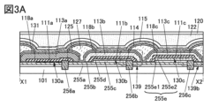
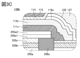
- 3A to 3C are cross-sectional views showing examples of display devices.
- 4A and 4B are cross-sectional views showing an example of the display device.
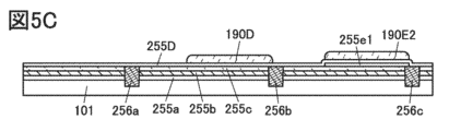
- 5A to 5E are cross-sectional views illustrating an example of a method for manufacturing a display device.
- 6A to 6D are cross-sectional views illustrating an example of a method for manufacturing a display device.
- 7A to 7C are cross-sectional views illustrating an example of a method for manufacturing a display device.
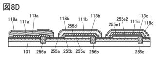
- 8A to 8D are cross-sectional views illustrating an example of a method for manufacturing a display device.
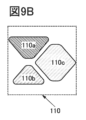
- 9A to 9F are top views showing examples of pixels.
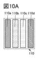
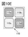
- FIG. 10A to 10H are top views showing examples of pixels.
- 11A to 11J are top views showing examples of pixels.
- 12A to 12D are top views showing examples of pixels.
- 12E to 12G are cross-sectional views showing examples of display devices.
- 13A and 13B are perspective views showing an example of a display device.
- 14A and 14B are cross-sectional views showing examples of display devices.
- FIG. 15 is a cross-sectional view showing an example of a display device.
- FIG. 16 is a cross-sectional view showing an example of a display device.
- FIG. 17 is a cross-sectional view showing an example of a display device.
- FIG. 18 is a cross-sectional view showing an example of a display device.
- FIG. 19 is a cross-sectional view showing an example of a display device.
- FIG. 15 is a cross-sectional view showing an example of a display device.
- FIG. 16 is a cross-sectional view showing an example of a display
- FIG. 20 is a perspective view showing an example of a display device.
- FIG. 21A is a cross-sectional view showing an example of a display device.
- 21B and 21C are cross-sectional views showing examples of transistors.
- FIG. 22A is a block diagram showing an example of a display device.
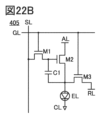
- 22B to 22D are diagrams showing examples of pixel circuits.
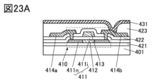
- 23A to 23D are diagrams illustrating examples of transistors.
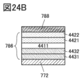
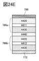
- 24A to 24F are diagrams showing configuration examples of light-emitting devices.
- 25A to 25D are diagrams illustrating examples of electronic devices.
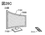
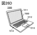
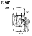
- 26A to 26F are diagrams illustrating examples of electronic devices.
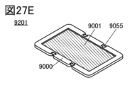
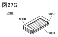
- 27A to 27G are diagrams illustrating examples of electronic devices.
- a display device may be read as an electronic device.
- a display device which is one mode of a display device, has a function of displaying (outputting) an image or the like on a display surface. Therefore, a display device is one aspect of an output device.
- the substrate of the display device is attached with a connector such as FPC (Flexible Printed Circuit) or TCP (Tape Carrier Package), or the substrate is mounted with a COG (Chip On Glass) method, etc. is sometimes called a display module.
- the display device may be referred to as a display panel.
- film and “layer” can be used interchangeably.
- conductive layer or “insulating layer” may be interchangeable with the terms “conductive film” or “insulating film.”
- an EL layer is a layer provided between a pair of electrodes of a light-emitting device (also referred to as a light-emitting element) and containing at least a light-emitting substance (also referred to as a light-emitting layer), or a laminate including a light-emitting layer.
- a device manufactured using a metal mask or FMM may be referred to as a device with an MM (metal mask) structure.
- a device manufactured without using a metal mask or FMM may be referred to as a device with an MML (metal maskless) structure.
- holes or electrons are sometimes referred to as “carriers”.
- the hole injection layer or electron injection layer is referred to as a "carrier injection layer”
- the hole transport layer or electron transport layer is referred to as a “carrier transport layer”
- the hole blocking layer or electron blocking layer is referred to as a "carrier It is sometimes called a block layer.
- the carrier injection layer, the carrier transport layer, and the carrier block layer described above may not be clearly distinguished from each other due to their cross-sectional shape, characteristics, or the like.
- one layer may serve as two or three functions of the carrier injection layer, the carrier transport layer, and the carrier block layer.
- One embodiment of the present invention is a display device having a display portion capable of full-color display.
- the display unit has first sub-pixels and second sub-pixels that emit different colors of light.
- the first subpixel has a first light emitting device that emits light of a first color and the second subpixel has a second light emitting device that emits light of a different color than the first light emitting device. have.
- the first light emitting device and the second light emitting device comprise at least one different material, for example different light emitting materials.
- the display device of one embodiment of the present invention uses light-emitting devices that are separately manufactured for each emission color.
- a structure in which light-emitting layers are separately formed or painted separately for light-emitting devices of each color is sometimes called an SBS (side-by-side) structure.
- SBS side-by-side
- the material and structure can be optimized for each light-emitting device, so the degree of freedom in selecting the material and structure increases, and it becomes easy to improve luminance and reliability.
- an island shape indicates a state in which two or more layers using the same material formed in the same step are physically separated.
- an island-shaped light-emitting layer means that the light-emitting layer is physically separated from an adjacent light-emitting layer.
- an island-shaped light-emitting layer can be formed by a vacuum evaporation method using a metal mask (also referred to as a shadow mask).
- a metal mask also referred to as a shadow mask.
- island-like structures are formed due to various influences such as precision of the metal mask, misalignment between the metal mask and the substrate, bending of the metal mask, and broadening of the contour of the deposited film due to vapor scattering.
- the shape and position of the light-emitting layer in (1) deviate from the design, it is difficult to increase the definition and aperture ratio of the display device.
- the layer profile may be blurred and the edge thickness may be reduced. In other words, the thickness of the island-shaped light-emitting layer may vary depending on the location.
- the manufacturing yield will be low due to low dimensional accuracy of the metal mask and deformation due to heat or the like.
- a first layer (which can be referred to as an EL layer or part of an EL layer) including a light-emitting layer that emits light of a first color is formed over one surface.
- a first mask layer is formed on the first layer.
- a first resist mask is formed over the first mask layer, and the first layer and the first mask layer are processed using the first resist mask, thereby forming an island-shaped first layer.
- a second layer (which can be referred to as an EL layer or part of an EL layer) including a light-emitting layer that emits light of a second color is covered with a second mask layer. and an island shape using a second resist mask.
- the mask layer is positioned above at least the light-emitting layer (more specifically, among the layers constituting the EL layer, the layer is processed into an island shape) and is used during the manufacturing process. , has a function of protecting the light-emitting layer.
- the light-emitting layer when processing the light-emitting layer into an island shape, a structure in which the light-emitting layer is processed using a photolithography method right above the light-emitting layer is conceivable. In the case of such a structure, the light-emitting layer may be damaged (damage due to processing, etc.) and the reliability may be significantly impaired.
- a layer positioned above the light-emitting layer for example, a carrier-transporting layer, a carrier-blocking layer, or a carrier-injecting layer, more specifically an electron-transporting layer
- a method in which a mask layer or the like is formed on a hole blocking layer, an electron injection layer, or the like, and the light emitting layer is processed into an island shape By applying the method, a highly reliable display device can be provided.
- an island-shaped EL layer manufactured by a method for manufacturing a display device of one embodiment of the present invention or an island-shaped layer formed of part of an EL layer is formed using a metal mask with a fine pattern. Instead, it is formed by forming an EL layer or an island-shaped layer made of a part of the EL layer over one surface and then processing the layer. Therefore, it is possible to realize a high-definition display device or a display device with a high aperture ratio, which has hitherto been difficult to achieve. Further, since an EL layer or an island-shaped layer composed of a part of the EL layer can be separately formed for each color, a display device with extremely vivid, high-contrast, and high-quality display can be realized.
- the EL layer or the island-shaped layer formed of part of the EL layer is subjected during the manufacturing process of the display device. Damage can be reduced and the reliability of the light-emitting device can be improved.
- the distance between adjacent light-emitting devices can be narrowed down to 1 ⁇ m or less.
- the distance between adjacent light emitting devices can be narrowed to 500 nm or less, 200 nm or less, 100 nm or less, or even 50 nm or less.
- the aperture ratio can be brought close to 100%.
- the aperture ratio can be 50% or more, 60% or more, 70% or more, 80% or more, or even 90% or more, and less than 100%.
- the pattern of the EL layer or the island-shaped layer itself formed of part of the EL layer can be made much smaller than in the case of using a metal mask.
- a metal mask is used for separately forming an EL layer or an island-shaped layer composed of a part of the EL layer, so the thickness varies between the center and the edge of the pattern, so the total area of the pattern is reduced. As a result, the effective area that can be used as the light emitting region is reduced.
- an island-shaped EL layer or an island-shaped layer composed of a part of the EL layer can be formed with a uniform thickness. . Therefore, almost the entire area of even a fine pattern can be used as a light emitting region. Therefore, a display device having both high definition and high aperture ratio can be manufactured.
- the EL layer or the EL layer is formed. It is preferable to form a mask layer on the island-shaped layer consisting of a part. Then, a resist mask is formed over the mask layer, and the EL layer or part of the EL layer and the mask layer are processed using the resist mask, so that the island-shaped EL layer or part of the EL layer is formed. It is preferable to form island-shaped layers.
- the layers included in the EL layer include a light emitting layer, a carrier injection layer (hole injection layer and electron injection layer), a carrier transport layer (hole transport layer and electron transport layer), and a carrier block layer (hole block layer and electron block layer).
- a carrier injection layer hole injection layer and electron injection layer
- a carrier transport layer hole transport layer and electron transport layer
- a carrier block layer hole block layer and electron block layer
- a layer (sometimes referred to as a common layer) and a common electrode (also referred to as an upper electrode) are formed in common (as one film) for the light emitting devices of each color.
- a carrier injection layer and a common electrode can be formed in common for each color light emitting device.
- the carrier injection layer is often a layer with relatively high conductivity among the EL layers. Therefore, the light-emitting device may be short-circuited when the carrier injection layer comes into contact with the side surface of a part of the EL layer formed like an island or the side surface of the pixel electrode. Note that even in the case where the carrier injection layer is provided in an island shape and the common electrode is formed in common for the light emitting devices of each color, the common electrode is in contact with the side surface of the EL layer or the side surface of the pixel electrode, so that light emission is prevented. The device may short out.
- the display device of one embodiment of the present invention includes an insulating layer covering at least side surfaces of the island-shaped light-emitting layer.
- the insulating layer may cover part of the top surface of the island-shaped light-emitting layer.
- the side surface of the island-shaped light-emitting layer as used herein refers to a surface of the interface between the island-shaped light-emitting layer and another layer that is not parallel to the substrate (or the surface on which the light-emitting layer is formed). Also, it is not necessarily a mathematically exact plane or curved surface.
- the insulating layer is provided thinly.
- the insulating layer is subjected to treatment such as heat treatment during manufacturing of the display device of one embodiment of the present invention, and the treatment may cause shrinkage of the insulating layer. Stress due to shrinkage of the insulating layer may be applied to each layer constituting the light emitting device. In such a case, if the insulating layer is too thick, the stress increases, and peeling may occur at the interface between the layers constituting the light emitting device. By providing a thin insulating layer, peeling can be suppressed and the reliability of the light-emitting device can be improved.
- the thickness of the adjacent insulating layer may be thicker than in a light-emitting device in which the top surface of the EL layer is high. . In this way, variations occur in the thickness of the insulating layer. In addition to the thickness, if unevenness occurs in the film, for example, there is a concern that variations in top surface shape may occur in addition to variations in thickness.
- the heights of the top surfaces of the island-shaped EL layers or the island-shaped layers formed of part of the EL layers included in adjacent light-emitting devices are approximately the same, so that the insulating layer is covered with the insulating layer.
- the unevenness of the formation surface can be made uniform, and the thickness of the insulating layer can be uniformly thinned.
- an island-shaped EL layer included in the first light-emitting device or an island-shaped EL layer formed of part of the EL layer is included in the first light-emitting device.
- the height difference between the top surfaces of the island-shaped EL layers of two adjacent light-emitting devices can be reduced.
- the insulating layer covering the side surface of the island-shaped light-emitting layer has a function as a barrier insulating layer against at least one of water and oxygen. Further, the insulating layer preferably has a function of suppressing diffusion of at least one of water and oxygen. In addition, the insulating layer preferably has a function of capturing or fixing at least one of water and oxygen (also referred to as gettering).
- a barrier insulating layer means an insulating layer having a barrier property.
- barrier property refers to a function of suppressing diffusion of a corresponding substance (also referred to as low permeability).
- the corresponding substance has a function of capturing or fixing (also called gettering).
- an insulating layer having a function as a barrier insulating layer or a gettering function it is possible to suppress entry of impurities (typically, at least one of water and oxygen) that can diffuse into each light-emitting device from the outside. possible configuration. With such a structure, a highly reliable light-emitting device and a highly reliable display device can be provided.
- impurities typically, at least one of water and oxygen
- a display device of one embodiment of the present invention includes a pixel electrode functioning as an anode, and an island-shaped hole-injection layer, a hole-transport layer, a light-emitting layer, and an electron layer provided in this order on the pixel electrode.
- a common electrode provided on the electron injection layer and functioning as a cathode;
- a display device of one embodiment of the present invention includes a pixel electrode functioning as a cathode, and an island-shaped electron-injection layer, an electron-transport layer, a light-emitting layer, and a positive electrode which are provided in this order over the pixel electrode.
- a hole-injection layer, an electron-injection layer, or the like is often a layer having relatively high conductivity among EL layers.
- the side surfaces of these layers are covered with the insulating layer; therefore, contact with a common electrode or the like can be suppressed. Therefore, short-circuiting of the light-emitting device can be suppressed, and the reliability of the light-emitting device can be improved.
- the island-shaped EL layer or the insulating layer covering the side surface of the island-shaped layer formed of part of the EL layer may have a single-layer structure or a stacked-layer structure.
- the insulating layer can be used as a protective insulating layer for the EL layer or an island-shaped layer formed of part of the EL layer.
- the protective insulating layer preferably covers part of the upper surface of the EL layer or an island-shaped layer formed of part of the EL layer.
- the mask layer may remain between the protective insulating layer and the top surface of the EL layer or an island-shaped layer formed of part of the EL layer.
- the mask layer is preferably an insulating layer using an inorganic material, like the protective insulating layer.
- the first insulating layer is formed using an inorganic insulating material because it is in contact with the EL layer or an island-shaped layer formed of part of the EL layer. is preferred.
- ALD atomic layer deposition
- the inorganic insulating layer is formed using a sputtering method, a chemical vapor deposition (CVD) method, or a plasma enhanced CVD (PECVD) method, which has a higher film formation rate than the ALD method. preferably formed. Accordingly, a highly reliable display device can be manufactured with high productivity.
- the second insulating layer is preferably formed using an organic material so as to planarize the concave portion formed in the first insulating layer.
- an aluminum oxide film formed by an ALD method can be used as the first insulating layer, and an organic resin film can be used as the second insulating layer.
- the organic resin it is preferable to use, for example, a photosensitive acrylic resin.
- organic solvents and the like that may be contained in the organic resin film may damage the EL layer.
- an inorganic insulating film such as an aluminum oxide film formed by an ALD method as the first insulating layer, the organic resin film and the side surface of the EL layer are not in direct contact with each other. This can prevent the EL layer from being dissolved by the organic solvent.
- the display device of one embodiment of the present invention it is not necessary to provide an insulating layer covering the end portion of the pixel electrode between the pixel electrode and the EL layer; can. Therefore, it is possible to achieve high definition or high resolution of the display device. Moreover, a mask for forming the insulating layer is not required, and the manufacturing cost of the display device can be reduced.
- the viewing angle dependency of the display device of one embodiment of the present invention can be extremely reduced. By reducing the viewing angle dependency, it is possible to improve the visibility of the image on the display device.
- the viewing angle (the maximum angle at which a constant contrast ratio is maintained when the screen is viewed obliquely) is 100° or more and less than 180°, preferably 150°. It can be in the range of 170° or more. It should be noted that the above viewing angle can be applied to each of the vertical and horizontal directions.
- [Configuration example of display device] 1 to 4 show a display device of one embodiment of the present invention.
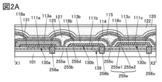
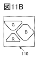
- FIG. 1 shows a top view of the display device 100.
- the display device 100 has a display section in which a plurality of pixels 110 are arranged, and a connection section 140 outside the display section.
- a plurality of sub-pixels are arranged in a matrix in the display section.
- FIG. 1 shows sub-pixels of 2 rows and 6 columns, which constitute pixels of 2 rows and 2 columns.
- the connection portion 140 can also be called a cathode contact portion.
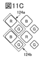
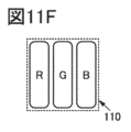
- a stripe arrangement is applied to the pixels 110 shown in FIG.
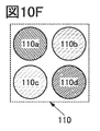
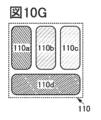
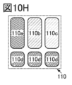
- the pixel 110 shown in FIG. 1 is composed of three sub-pixels, sub-pixels 110a, 110b and 110c.
- the sub-pixels 110a, 110b, 110c each have light emitting devices that emit different colors of light.
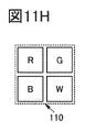
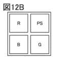
- the sub-pixels 110a, 110b, and 110c include sub-pixels of three colors of red (R), green (G), and blue (B), and three colors of yellow (Y), cyan (C), and magenta (M). sub-pixels and the like. Also, the number of types of sub-pixels is not limited to three, and may be four or more.
- the four sub-pixels are R, G, B, and white (W) sub-pixels, R, G, B, and Y sub-pixels, and R, G, B, infrared light ( IR), four sub-pixels, and so on.
- the row direction is sometimes called the X direction
- the column direction is sometimes called the Y direction.
- the X and Y directions intersect, for example, are orthogonal (see FIG. 1).
- FIG. 1 shows an example in which sub-pixels of different colors are arranged side by side in the X direction and sub-pixels of the same color are arranged side by side in the Y direction.
- connection portion 140 is positioned below the display portion when viewed from above
- the connecting portion 140 may be provided at least one of the upper side, the right side, the left side, and the lower side of the display portion when viewed from above, and may be provided so as to surround the four sides of the display portion.
- the shape of the upper surface of the connecting portion 140 may be strip-shaped, L-shaped, U-shaped, frame-shaped, or the like.
- the number of connection parts 140 may be singular or plural.
- FIG. 2A shows a cross-sectional view along the dashed-dotted line X1-X2 in FIG.
- FIG. 2B shows an enlarged view of region 139 shown in FIG. 2A.
- FIG. 2C shows a cross-sectional view along the dashed-dotted line Y1-Y2 in FIG.
- FIG. 2D shows an example of a configuration different from that of FIG. 2C.
- the display device 100 is provided with insulating layers 255a, 255b, 255c, 255d, and 255e over the layer 101 including transistors.
- Light-emitting devices 130a, 130b, and 130c are provided on the insulating layer, and a protective layer 131 is provided to cover these light-emitting devices.
- Light emitting device 130a is, for example, a light emitting device corresponding to subpixel 110a
- light emitting device 130b is, for example, a light emitting device corresponding to subpixel 110b
- light emitting device 130c is, for example, a light emitting device corresponding to subpixel 110c.
- a substrate 120 is bonded onto the protective layer 131 with a resin layer 122 .
- An insulating layer 125 and an insulating layer 127 on the insulating layer 125 are provided in a region between adjacent light emitting devices.
- an island-shaped insulating layer 255d and an island-shaped insulating layer 255e are provided over the insulating layer 255c.
- the light emitting device 130a is provided on the insulating layer 255c.
- Light emitting device 130b is provided on insulating layer 255d.
- the light emitting device 130c is provided on the insulating layer 255e.
- the light-emitting device 130a includes a pixel electrode 111a on the insulating layer 255c, an island-shaped layer 113a on the pixel electrode 111a, a common layer 114 on the island-shaped layer 113a, and a common electrode 115 on the common layer 114. have.
- layer 113a and common layer 114 can be collectively referred to as EL layers.
- the pixel electrode 111a contacts, for example, the upper surface of the insulating layer 255c in at least part of the light emitting region of the light emitting device 130a.
- the light-emitting device 130b includes a pixel electrode 111b on the insulating layer 255d, an island-shaped layer 113b on the pixel electrode 111b, a common layer 114 on the island-shaped layer 113b, and a common electrode 115 on the common layer 114. have.
- layer 113b and common layer 114 can be collectively referred to as EL layers.
- the pixel electrode 111b is in contact with, for example, the upper surface of the insulating layer 255d in at least part of the light emitting region of the light emitting device 130b. In some cases, the pixel electrode 111b has a region in contact with the upper surface of the insulating layer 255c at the end.
- the light-emitting device 130c includes a pixel electrode 111c on the insulating layer 255e, an island-shaped layer 113c on the pixel electrode 111c, a common layer 114 on the island-shaped layer 113c, and a common electrode 115 on the common layer 114. have.
- layer 113c and common layer 114 can be collectively referred to as EL layers.
- the insulating layer 255e may have a laminated structure of an insulating layer 255e1 and an insulating layer 255e2 on the insulating layer 255e1. They are formed from the same insulating film.
- the thickness of the insulating layer 255d and the layer formed from the same insulating film as the insulating layer 255d are substantially the same.
- the pixel electrode 111c is in contact with, for example, the upper surface of the insulating layer 255e. In some cases, the pixel electrode 111c has a region in contact with the upper surface of the insulating layer 255c at the end.
- a plurality of plugs 256 are provided to bury part of the layer 101 including the transistor, the insulating layer 255a, the insulating layer 255b, and the insulating layer 255c.
- Each of the plurality of plugs 256 has a function of electrically connecting the semiconductor element provided in the layer 101 including the transistor and the pixel electrode of the light emitting device.
- the plug 256 electrically connected to the pixel electrode 111a is represented as a plug 256a
- the plug 256 electrically connected to the pixel electrode 111b is represented as a plug 256b
- the plug 256 is electrically connected to the pixel electrode 111c.
- the plug 256 that is connected is denoted as plug 256c.
- Materials that can be used for plug 256 include metals such as aluminum, titanium, chromium, nickel, copper, yttrium, zirconium, molybdenum, gold, silver, platinum, magnesium, iron, cobalt, palladium, tantalum, or tungsten. Examples include alloys containing materials, nitrides of these metal materials, and the like. As the plug 256, a film containing these materials can be used as a single layer or as a laminated structure.
- a single-layer structure of an aluminum film containing silicon a two-layer structure in which an aluminum film is stacked over a titanium film, a two-layer structure in which an aluminum film is stacked over a tungsten film, and a copper film over a copper-magnesium-aluminum alloy film.
- plug 256 is formed to be embedded in insulating layer 255c.
- the top surface of the plug 256 and the top surface of the insulating layer 255c are generally aligned with each other, eg, as shown in FIGS. 2A and 2B.
- the top surface of the insulating layer 255c may have a region that is continuous with the plug 256 . In the region forming a continuous plane, the height of the top surface of the insulating layer 255c is approximately the same as the height of the top surface of the plug 256 .
- the height of the insulating layer 255c and the height of the upper surface of the plug are approximately the same means that the height difference between them is, for example, 100 nm or less, 50 nm or less, 30 nm or less, or 10 nm or less.
- the pixel electrode 111a preferably has a region in contact with the upper surface of the insulating layer 255c and a region in contact with the upper surface of the plug 256a.
- the pixel electrode 111b preferably has a region in contact with the upper surface of the insulating layer 255d and a region in contact with the upper surface of the plug 256b.
- the pixel electrode 111b may have a region in contact with the upper surface of the insulating layer 255c, as shown in FIG. 2A and the like.
- the pixel electrode 111b is provided, for example, so as to cover the upper surface and side surfaces of the insulating layer 255d.
- the insulating layer 255d is provided so as not to cover at least part of the upper surface of the plug 256b. Accordingly, after exposing a part of the upper surface of the plug 256b, the pixel electrode 111b can be formed so as to cover the exposed upper surface. can be configured to be in contact with the upper surface of the .
- insulating layer 255d has a first end that overlaps plug 256b.
- the first end overlaps the pixel electrode 111b, and the pixel electrode 111b has a second end extending outward from the first end.
- the first end preferably contacts the top surface of plug 256b. Also, the first end preferably contacts the lower surface of the pixel electrode 111b.
- the first side surface of the insulating layer 255d is covered with the pixel electrode 111b. Also, the second side surface of the insulating layer 255e is covered with the pixel electrode 111c.
- the pixel electrode 111c preferably has a region in contact with the upper surface of the insulating layer 255e and a region in contact with the upper surface of the plug 256c. Also, as shown in FIG. 2A and the like, the pixel electrode 111c may have a region in contact with the upper surface of the insulating layer 255c. Also, the pixel electrode 111c is provided, for example, so as to cover the upper surface and side surfaces of the insulating layer 255e.
- the insulating layer 255e is provided so as not to cover at least part of the top surface of the plug 256c.
- the pixel electrode 111c can be formed so as to cover the exposed upper surface. can be configured to contact the upper surface of the .
- insulating layer 255e has a third end that overlaps plug 256c. Also, the third end overlaps with the pixel electrode 111c, and the pixel electrode 111c has a fourth end extending outward from the third end. The third end preferably contacts the top surface of plug 256c. Also, the third end preferably contacts the lower surface of the pixel electrode 111c.
- FIG. 3A shows an example of a configuration different from that in FIG. 2A as a cross-sectional view taken along the dashed-dotted line X1-X2 in FIG.
- plug 256a, plug 256b, and plug 256c each have a region protruding from insulating layer 255c.
- the pixel electrode 111a covers the side surface of the plug 256a
- the pixel electrode 111b covers the side surface of the plug 256b
- the pixel electrode 111c covers the side surface of the plug 256c. It differs from FIG. 2A in that it has a configuration.
- the plug 256 is formed to be embedded in the insulating layer 255c.
- the upper surface of the insulating layer 255c has, for example, a region forming a continuous surface with the plug 256 .
- the height of the top surface of the insulating layer 255c is approximately the same as the height of the top surface of the plug 256 .
- the top surface of the plug 256 is higher than the top surface of the insulating layer 255c.
- the pixel electrode 111a preferably has a region in contact with the side surface of the plug 256a.
- the pixel electrode 111b preferably has a region in contact with the side surface of the plug 256b.
- the pixel electrode 111c preferably has a region in contact with the side surface of the plug 256c.
- the pixel electrode 111a has a region covering the top surface of the plug 256a
- the pixel electrode 111b has a region covering the top surface of the plug 256b
- the pixel electrode 111c has a region covering the top surface of the plug 256c.
- FIG. 3B is an enlarged view of region 139 shown in FIG. 3A.
- the side surface of the plug 256b protrudes from the insulating layer 255a, the insulating layer 255b, the insulating layer 255c, and the insulating layer 255c. and a region covered with none of the layer 255a, the insulating layer 255b, and the insulating layer 255c.
- the region protruding from the insulating layer 255c is covered with the pixel electrode 111b.
- FIG. 3C is an enlarged view of region 139b shown in FIG. 3A.
- the side surface of the plug 256c protrudes from a region covered with the insulating layer 255a, a region covered with the insulating layer 255b, a region covered with the insulating layer 255c, and the insulating layer 255c. and a region covered with neither the insulating layer 255b nor the insulating layer 255c.
- the region protruding from the insulating layer 255c is covered with the pixel electrode 111c.
- FIGS. 4A and 4B a structure in which the pixel electrode does not cover the upper surface of the plug 256 may be employed.
- FIG. 4A is an example of an enlarged cross-sectional view of the plug 256b and its vicinity.
- FIG. 4B is an example of an enlarged cross-sectional view of the plug 256c and its vicinity.
- the first side surface of the insulating layer 255d and the first side surface of the plug 256b are substantially aligned.
- the first side surface of the insulating layer 255d and the first side surface of the plug 256b form a continuous surface, and the pixel electrode 111b covers the continuous surface.
- the first side surface of the insulating layer 255e and the first side surface of the plug 256c are substantially aligned.
- the first side surface of the insulating layer 255e and the first side surface of the plug 256c form a continuous surface, and the pixel electrode 111c covers the continuous surface.
- the height of the top surface of the EL layer included in the light-emitting device 130a, the height of the top surface of the EL layer included in the light-emitting device 130b, and the height of the top surface of the EL layer included in the light-emitting device 130c are preferably substantially aligned.
- the difference in the height of the top surfaces of the EL layers of the light emitting devices 130 is preferably 100 nm or less, more preferably 50 nm or less, and even more preferably 30 nm or less.
- the top surface of the layer 113a, the top surface of the layer 113b, and the top surface of the layer 113c are preferably substantially the same.
- the difference between the top surfaces of the layers 113 of the light emitting devices 130 is preferably 100 nm or less, more preferably 50 nm or less, and even more preferably 30 nm or less.
- the sum of the thickness of the pixel electrode 111a and the thickness of the layer 113a is approximately the sum of the thickness of the pixel electrode 111b, the thickness of the layer 113b, and the thickness of the insulating layer 255d. Alignment is preferred.
- the sum of the thickness of the pixel electrode 111b, the thickness of the layer 113b, and the thickness of the insulating layer 255d is the sum of the thickness of the pixel electrode 111c, the thickness of the layer 113c, and the thickness of the insulating layer 255e. It is preferable that they are roughly aligned.
- the sum of the thickness of the pixel electrode 111a and the thickness of the EL layer included in the light-emitting device 130a is the thickness of the pixel electrode 111b, the thickness of the EL layer included in the light-emitting device 130b, and the sum of the thicknesses of the insulating layer 255d.
- the sum of the thickness of the pixel electrode 111b, the thickness of the EL layer included in the light-emitting device 130b, and the thickness of the insulating layer 255d is the thickness of the pixel electrode 111c, the thickness of the EL layer included in the light-emitting device 130c, and the thickness of the EL layer included in the light-emitting device 130c. It is preferable that the sum of the thicknesses of the insulating layers 255e be approximately the same.
- the display device 100 can be configured to have one insulating layer 125 and one insulating layer 127, for example.
- the display device 100 may have a plurality of insulating layers 125 separated from each other, and may have a plurality of insulating layers 127 separated from each other.
- a display device of one embodiment of the present invention is a top emission type in which light is emitted in a direction opposite to a substrate over which a light-emitting device is formed, and light is emitted toward a substrate over which a light-emitting device is formed.
- a bottom emission type bottom emission type
- a double emission type dual emission type in which light is emitted from both sides may be used.
- a stacked-layer structure in which a plurality of transistors are provided over a substrate and an insulating layer is provided to cover the transistors can be applied.
- An insulating layer over a transistor may have a single-layer structure or a stacked-layer structure.
- FIG. 2A and the like show an insulating layer 255a, an insulating layer 255b over the insulating layer 255a, and an insulating layer 255c over the insulating layer 255b among the insulating layers over the transistor. These insulating layers may have recesses between adjacent light emitting devices.
- FIG. 2A and the like show an example in which a concave portion is provided in the insulating layer 255c.
- various inorganic insulating films such as an oxide insulating film, a nitride insulating film, an oxynitride insulating film, and a nitride oxide insulating film are preferably used.
- an oxide insulating film or an oxynitride insulating film such as a silicon oxide film, a silicon oxynitride film, or an aluminum oxide film is preferably used.
- a nitride insulating film or a nitride oxide insulating film such as a silicon nitride film or a silicon nitride oxide film is preferably used. More specifically, a silicon oxide film is preferably used for the insulating layers 255a and 255c, and a silicon nitride film is preferably used for the insulating layer 255b.
- the insulating layer 255b preferably functions as an etching protection film.
- oxynitride refers to a material whose composition contains more oxygen than nitrogen
- nitride oxide refers to a material whose composition contains more nitrogen than oxygen. point to the material.
- silicon oxynitride refers to a material whose composition contains more oxygen than nitrogen
- silicon nitride oxide refers to a material whose composition contains more nitrogen than oxygen. indicates
- FIG. 1 A structural example of the layer 101 including a transistor will be described later in Embodiments 3 and 4.
- FIG. 1 A structural example of the layer 101 including a transistor will be described later in Embodiments 3 and 4.
- FIG. 1 A structural example of the layer 101 including a transistor will be described later in Embodiments 3 and 4.
- Light emitting devices 130a, 130b, 130c each emit different colors of light.
- Light-emitting devices 130a, 130b, and 130c are preferably a combination that emits three colors of light, red (R), green (G), and blue (B), for example.
- Examples of the light-emitting devices 130a, 130b, and 130c include OLEDs (Organic Light Emitting Diodes) and QLEDs (Quantum-dot Light Emitting Diodes).
- Examples of the light-emitting substance included in the light-emitting device include a substance that emits fluorescence (fluorescent material), a substance that emits phosphorescence (phosphorescent material), and a substance that exhibits thermally activated delayed fluorescence (thermally activated delayed fluorescence: TADF) material. ) and the like.
- As a light-emitting substance included in the EL element not only an organic compound but also an inorganic compound (quantum dot material, etc.) can be used.
- the TADF material a material in which a singlet excited state and a triplet excited state are in thermal equilibrium may be used. Since such a TADF material has a short emission lifetime (excitation lifetime), it is possible to suppress a decrease in emission efficiency in a high-luminance region of a light-emitting device.
- a light-emitting device has an EL layer between a pair of electrodes.
- the EL layer has at least a light-emitting layer.
- one of a pair of electrodes may be referred to as a pixel electrode and the other may be referred to as a common electrode.
- one electrode functions as an anode and the other electrode functions as a cathode.
- the case where the pixel electrode functions as an anode and the common electrode functions as a cathode may be taken as an example.
- the structure of the light-emitting device of this embodiment is not particularly limited, and may be a single structure or a tandem structure.
- the symbols added to the reference numerals may be omitted and the light-emitting device 130 may be used for description.
- the layers 113a, 113b, and 113c are also referred to as layers 113 in some cases.
- the pixel electrode 111a, the pixel electrode 111b, and the pixel electrode 111c may also be described as the pixel electrode 111 in some cases.
- island-shaped layers provided for each light-emitting device are indicated as layers 113a, 113b, and 113c, and a layer shared by a plurality of light-emitting devices is indicated. Shown as common layer 114 . Note that in this specification and the like, the layers 113a, 113b, and 113c may be referred to as EL layers without including the common layer 114 in some cases.
- Layers 113a, 113b, and 113c have at least a light-emitting layer.
- the layer 113a has a light-emitting layer that emits red light
- the layer 113b has a light-emitting layer that emits green light
- the layer 113c has a light-emitting layer that emits blue light.
- Layers 113a, 113b, and 113c are each one of a hole-injection layer, a hole-transport layer, a hole-blocking layer, a charge-generating layer, an electron-blocking layer, an electron-transporting layer, and an electron-injecting layer. You may have more than
- layers 113a, 113b, and 113c may have a hole-injection layer, a hole-transport layer, a light-emitting layer, and an electron-transport layer. Moreover, you may have an electron block layer between a hole transport layer and a light emitting layer. Moreover, you may have an electron injection layer on the electron transport layer.
- the layers 113a, 113b, and 113c may have an electron-injection layer, an electron-transport layer, a light-emitting layer, and a hole-transport layer in this order.
- a hole blocking layer may be provided between the electron transport layer and the light emitting layer.
- a hole injection layer may be provided on the hole transport layer.
- Layers 113a, 113b, and 113c preferably have a light-emitting layer and a carrier-transport layer (electron-transport layer or hole-transport layer) over the light-emitting layer.
- the surfaces of the layers 113a, 113b, and 113c are exposed during the manufacturing process of the display device. Damage to the layer can be reduced. This can improve the reliability of the light emitting device.
- the layers 113a, 113b, and 113c have, for example, a first light-emitting unit, a charge-generating layer, and a second light-emitting unit.
- the layer 113a has two or more light-emitting units that emit red light
- the layer 113b has two or more light-emitting units that emit green light
- the layer 113c emits blue light.
- a configuration having two or more light-emitting units is preferable.
- the second light-emitting unit preferably has a light-emitting layer and a carrier-transporting layer (electron-transporting layer or hole-transporting layer) on the light-emitting layer. Since the surface of the second light-emitting unit is exposed during the manufacturing process of the display device, by providing the carrier transport layer on the light-emitting layer, the exposure of the light-emitting layer to the outermost surface is suppressed and damage to the light-emitting layer is prevented. can be reduced. This can improve the reliability of the light emitting device.
- a carrier-transporting layer electron-transporting layer or hole-transporting layer
- the common layer 114 has, for example, an electron injection layer or a hole injection layer.
- the common layer 114 may have a laminate of an electron transport layer and an electron injection layer, or may have a laminate of a hole transport layer and a hole injection layer.
- Common layer 114 is shared by light emitting devices 130a, 130b, 130c.
- the layers 113a to 113c preferably have different thicknesses.
- the thickness of each of the layers 113a to 113c may be set according to the optical path length that intensifies the emitted light. Thereby, a microcavity structure can be realized and the color purity in each light emitting device can be enhanced.
- the thickness of the layer 113 and the like may be set so that the optical path length is m ⁇ /2 (m is an integer equal to or greater than 1) or its vicinity with respect to the wavelength ⁇ of light obtained from the light emitting layer of the light emitting device.
- the layer 113a emitting light with the longest wavelength is the layer 113c, which is the thickest and emits light with the shortest wavelength, may be the thinnest.
- FIG. 2A shows an example in which among the layers 113a to 113c, the layer 113a is the thickest, the layer 113c is the thinnest, and the layer 113b is thinner than the layer 113a and thicker than the layer 113c.
- the present invention is not limited to this.
- the layer 113c included in the blue light-emitting device may be the thickest.
- each layer 113 is not limited to this, and the thickness of each layer 113 can be adjusted in consideration of the wavelength of light emitted by each light emitting device, the optical characteristics of the layers constituting the light emitting device, the electrical characteristics of the light emitting device, and the like.
- the optical path length in the light-emitting device can be adjusted not only by making the layers 113a to 113c different in thickness, but also by making the pixel electrodes 111a to 111c different in thickness.
- the pixel electrode 111 is a reflective electrode having a laminated structure of a reflective conductive material (reflective conductive film) and a translucent conductive material (transparent conductive film)
- different colors By making the thickness of the transparent conductive film different between the light-emitting devices exhibiting , it is possible to make the optical path length suitable for each color.
- the optical path length in the light-emitting device is determined, for example, by the sum of the thicknesses of the transparent conductive film of the pixel electrode 111, the layer 113, and the common layer 114.
- the drawings and the like in this specification may not show clearly different thicknesses of the layer 113 and the pixel electrode 111 in each light-emitting device, but the thickness is adjusted as appropriate in each light-emitting device. , preferably intensifies the light of the wavelength corresponding to the respective light emitting device.
- the difference in height between the top surfaces of the layers 113a to 113c is preferably small.
- the layers 113a to 113c may have substantially the same top surface height.
- the insulating layer 127 is provided so as to fill the recesses between the light emitting devices.
- the depth of the recess is determined, for example, according to the height difference between the top surface of the layer 113 and the top surface of the insulating layer 255c.
- the in-plane unevenness distribution of the surface on which the insulating layer 127 is formed can be reduced.
- the shape of the insulating layer 127 can be made into a suitable shape over in-plane. Specifically, for example, variations in the thickness of the insulating layer 127 can be reduced across the plane. In addition, since variations in the thickness of the insulating layer 127 can be reduced over the plane, the thickness of the insulating layer 127 can be reduced.
- the height difference between the top surface of the insulating layer 127 and the top surfaces of the layers 113a to 113c can be reduced.
- the difference between the top surface of the insulating layer 127 and the top surfaces of the layers 113a to 113c is preferably less than 200 nm, more preferably 100 nm or less.
- the difference between the height of the upper surface of the insulating layer 127 and the height of the upper surface of the layer 113a is preferably less than 200 nm, more preferably 100 nm or less.
- the difference between the height of the upper surface of the insulating layer 127 and the height of the upper surface of the layer 113b is preferably less than 200 nm, more preferably 100 nm or less.
- the difference between the height of the upper surface of the insulating layer 127 and the height of the upper surface of the layer 113c is preferably less than 200 nm, more preferably 100 nm or less.
- the height of the upper surface of layers such as the pixel electrode 111, the layer 113, and the insulating layer 127
- the upper surface is not flat, for example, the highest portion of the insulating layer 127 is measured.
- an insulating layer containing an organic material can be preferably used as the insulating layer 127.
- the unevenness can be planarized, for example.
- the insulating layer 127 When the insulating layer 127 is subjected to treatment such as heat treatment, the insulating layer 127 may shrink. Such shrinkage may stress the layers that make up light emitting device 130 . Such stress may cause peeling or the like at the interfaces of the layers constituting the light-emitting device 130 .
- the thickness of the adjacent insulating layer 127 is greater than in a light-emitting device in which the top surface of the layer 113 is high. may become.
- the thickness of the insulating layer 127 varies.
- variations in top surface shape may occur in addition to variations in thickness.
- peeling may occur at the interface between the insulating layer 127 and the insulating layer 125 . Note that peeling does not always occur between the insulating layer 127 and the insulating layer 125 and there is a concern that peeling may occur between the insulating layer 125 and the layer 113 .
- the film thickness of the insulating layer 127 can be uniformly thinned.
- the thickness of the insulating layer 127 can be uniformly reduced.
- the stress applied to each layer constituting the light emitting device 130 can be uniformly reduced.
- the top surface of the insulating layer 127 is preferably flat, but the surface may have a gently curved shape.
- the top surface of insulating layer 127 may be convex, concave, or planar.
- Each end of the pixel electrode 111a, the pixel electrode 111b, and the pixel electrode 111c preferably has a tapered shape.
- the layers 113a, 113b, and 113c provided along the side surfaces of the pixel electrodes also have tapered shapes.
- the side surface of the pixel electrode coverage of at least part of the EL layer provided along the side surface of the pixel electrode can be improved.
- the side surface of the pixel electrode is tapered because foreign matter (eg, dust or particles) in the manufacturing process can be easily removed by a treatment such as cleaning.
- a tapered shape refers to a shape in which at least a part of the side surface of the structure is inclined with respect to the substrate surface.
- the common electrode 115 is shared by the light emitting devices 130a, 130b, and 130c.
- a common electrode 115 shared by a plurality of light-emitting devices is electrically connected to the conductive layer 123 provided in the connecting portion 140 (see FIGS. 2C and 2D).
- a light-emitting layer or the like is not provided in the connecting portion 140 shown in FIGS. 2C and 2D. Therefore, in the step of forming an insulating film to be the insulating layer 127 , the upper surface of the conductive layer 123 is the formation surface of the connection portion 140 .
- the height difference between the top surface of the conductive layer 123 and the top surfaces of the layers 113a, 113b, and 113c is preferably small.
- the insulating layer 255e over the insulating layer 255c and provide the conductive layer 123 so as to cover the insulating layer 255e.
- the unevenness of the surface on which the insulating film to be the insulating layer 127 is formed can be reduced.
- At least part of the conductive layer 123 is preferably formed using the same material and in the same process as at least one of the pixel electrodes 111a to 111c. Note that an insulating layer is not necessarily provided between the conductive layer 123 and the insulating layer 255c. Further, an insulating layer 255d may be provided instead of the insulating layer 255e.
- FIG. 2C shows an example in which a common layer 114 is provided over the conductive layer 123 and the conductive layer 123 and the common electrode 115 are electrically connected through the common layer 114 .
- the common layer 114 may not be provided in the connecting portion 140 .
- the common layer 114 is not provided, and the conductive layer 123 and the common electrode 115 are directly connected.
- a mask also referred to as an area mask or a rough metal mask to distinguish from a fine metal mask
- the common layer 114 and the common electrode 115 are formed into a region where a film is formed. can be changed.
- the protective layer 131 may have a single layer structure or a laminated structure of two or more layers.
- the conductivity of the protective layer 131 does not matter. At least one of an insulating film, a semiconductor film, and a conductive film can be used as the protective layer 131 .
- the protective layer 131 By including an inorganic film in the protective layer 131, deterioration of the light-emitting device is suppressed, such as prevention of oxidation of the common electrode 115 and entry of impurities (moisture, oxygen, etc.) into the light-emitting device. Reliability can be improved.
- an inorganic insulating film such as an oxide insulating film, a nitride insulating film, an oxynitride insulating film, or a nitride oxide insulating film can be used.
- oxide insulating films include silicon oxide films, aluminum oxide films, gallium oxide films, germanium oxide films, yttrium oxide films, zirconium oxide films, lanthanum oxide films, neodymium oxide films, hafnium oxide films, and tantalum oxide films.
- the nitride insulating film include a silicon nitride film and an aluminum nitride film.
- the oxynitride insulating film examples include a silicon oxynitride film, an aluminum oxynitride film, and the like.
- the nitride oxide insulating film examples include a silicon nitride oxide film, an aluminum nitride oxide film, and the like.
- the protective layer 131 preferably includes a nitride insulating film or a nitride oxide insulating film, and more preferably includes a nitride insulating film.
- the protective layer 131 includes In—Sn oxide (also referred to as ITO), In—Zn oxide, Ga—Zn oxide, Al—Zn oxide, or indium gallium zinc oxide (In—Ga—Zn oxide).
- ITO In—Sn oxide
- In—Zn oxide Ga—Zn oxide
- Al—Zn oxide Al—Zn oxide
- indium gallium zinc oxide In—Ga—Zn oxide
- An inorganic film containing a material such as IGZO can also be used.
- the inorganic film preferably has a high resistance, and specifically, preferably has a higher resistance than the common electrode 115 .
- the inorganic film may further contain nitrogen.
- the protective layer 131 When the light emitted from the light-emitting device is taken out through the protective layer 131, the protective layer 131 preferably has high transparency to visible light.
- the protective layer 131 preferably has high transparency to visible light.
- ITO, IGZO, and aluminum oxide are preferable because they are inorganic materials with high transparency to visible light.
- the protective layer 131 for example, a stacked structure of an aluminum oxide film and a silicon nitride film over the aluminum oxide film, or a stacked structure of an aluminum oxide film and an IGZO film over the aluminum oxide film, or the like can be used. can be done. By using the stacked-layer structure, impurities (such as water and oxygen) entering the EL layer can be suppressed.
- the protective layer 131 may have an organic film.
- protective layer 131 may have both an organic film and an inorganic film.
- organic materials that can be used for the protective layer 131 include organic insulating materials that can be used for the insulating layer 127 described later.
- the protective layer 131 may have a two-layer structure formed using different film formation methods. Specifically, the first layer of the protective layer 131 may be formed using the ALD method, and the second layer of the protective layer 131 may be formed using the sputtering method.
- no insulating layer is provided between the pixel electrode 111a and the layer 113a to cover the edge of the upper surface of the pixel electrode 111a.
- no insulating layer is provided between the pixel electrode 111b and the layer 113b so as to cover the edge of the upper surface of the pixel electrode 111b. Therefore, the interval between adjacent light emitting devices can be made very narrow. Therefore, a high-definition or high-resolution display device can be obtained.
- the mask layer 118a is positioned on the layer 113a of the light emitting device 130a
- the mask layer 118b is positioned on the layer 113b of the light emitting device 130b
- the layer 113c of the light emitting device 130c is positioned.
- Overlying is mask layer 118c.
- the mask layer 118a is a portion of the mask layer that remains in contact with the upper surface of the layer 113a when the layer 113a is processed.
- the mask layers 118b and 118c are part of the mask layers provided when the layers 113b and 113c were formed, respectively.
- part of the mask layer used to protect the EL layer may remain during manufacturing.
- the same material may be used for any two or all of the mask layers 118a to 118c, or different materials may be used.
- the mask layer 118a, the mask layer 118b, and the mask layer 118c may be collectively called the mask layer 118 below.
- one edge of mask layer 118a is aligned or nearly aligned with an edge of layer 113a, and the other edge of mask layer 118a is located on layer 113a.
- the other end of the mask layer 118a preferably overlaps the layer 113a and the pixel electrode 111a.
- the other end of the mask layer 118a is likely to be formed on the substantially flat surface of the layer 113a.
- the mask layers 118b and 118c the mask layer 118 remains, for example, between the insulating layer 125 and the layer 113a, 113b, or 113c processed into an island shape.
- the mask layer 118 for example, one or more kinds of metal films, alloy films, metal oxide films, semiconductor films, organic insulating films, inorganic insulating films, and the like can be used.
- various inorganic insulating films that can be used for the protective layer 131 can be used.
- inorganic insulating materials such as aluminum oxide, hafnium oxide, and silicon oxide can be used.
- the insulating layer 125 and the insulating layer 127 preferably cover part of the upper surface of the island-shaped layer 113a, layer 113b, or layer 113c.
- the insulating layer 125 and the insulating layer 127 cover not only the side surfaces of the island-shaped layers 113a, 113b, and 113c but also the top surfaces thereof, so that peeling of the layers 113a, 113b, and 113c can be prevented. can be prevented, and the reliability of the light-emitting device can be improved. Moreover, the manufacturing yield of the light-emitting device can be further increased.
- FIG. 2A shows an example in which a laminated structure of a layer 113a, a mask layer 118a, an insulating layer 125, and an insulating layer 127 is positioned on the edge of the pixel electrode 111a.
- a laminated structure of a layer 113b, a mask layer 118b, an insulating layer 125, and an insulating layer 127 is positioned on the edge of the pixel electrode 111b, and a layer 113c and a mask layer 118c are positioned on the edge of the pixel electrode 111c.
- an insulating layer 125, and an insulating layer 127 are positioned.
- FIG. 2A and the like show an example in which the edge of the layer 113a is located outside the edge of the pixel electrode 111a.
- the pixel electrode 111a and the layer 113a are described as an example, the same applies to the pixel electrode 111b and the layer 113b and the pixel electrode 111c and the layer 113c.
- the layer 113a is formed to cover the edge of the pixel electrode 111a.
- the aperture ratio can be increased compared to a structure in which the end portions of the island-shaped layers 113a, 113b, and 113c are positioned inside the end portions of the pixel electrodes.
- the side surface of the pixel electrode with the layer 113a, the layer 113b, or the layer 113c, contact between the pixel electrode and the common electrode 115 can be suppressed, so short-circuiting of the light-emitting device can be suppressed. Further, the distance between the light emitting region of the EL layer (that is, the region overlapping with the pixel electrode) and the edge of the layer 113a, the layer 113b, or the layer 113c can be increased, so reliability can be improved.
- the insulating layer 125 preferably covers at least one side surface of the island-shaped layer 113a, layer 113b, or layer 113c, and more preferably covers both side surfaces of the island-shaped layer 113a, layer 113b, or layer 113c. .
- the insulating layer 125 can be in contact with each side surface of the island-shaped layer 113a, the layer 113b, or the layer 113c.
- the layer 113a covers the edge of the pixel electrode 111a and the insulating layer 125 is in contact with the side surface of the layer 113a.
- the edge of the pixel electrode 111b is covered with the layer 113b
- the edge of the pixel electrode 111c is covered with the layer 113c
- the insulating layer 125 is in contact with the side surface of the layer 113b and the side surface of the layer 113c.
- the insulating layer 127 is provided on the insulating layer 125 so as to fill the recess formed in the insulating layer 125 .
- the insulating layer 127 can overlap with part of the top surface and side surfaces of the layers 113a, 113b, and 113c with the insulating layer 125 interposed therebetween.
- insulating layer 125 and the insulating layer 127 By providing the insulating layer 125 and the insulating layer 127, a space between adjacent island-shaped layers can be filled; It is possible to reduce unevenness with a large height difference on the formation surface and make it more flat. Therefore, it is possible to improve the coverage of the carrier injection layer and the common electrode, and prevent the common electrode from being disconnected.
- Common layer 114 and common electrode 115 are provided on layers 113 a , 113 b , 113 c , mask layer 118 , insulating layer 125 and insulating layer 127 .
- the steps can be planarized, and coverage with the common layer 114 and the common electrode 115 can be improved. Therefore, it is possible to suppress poor connection due to disconnection. In addition, it is possible to prevent the common electrode 115 from being locally thinned due to the steps and increasing the electrical resistance.
- the top surface of the insulating layer 125 and the top surface of the insulating layer 127 are each at least one of the layers 113a, 113b, and 113c. It is preferred to align or approximately align with the height of the top surface at one end.
- the top surface of the insulating layer 127 preferably has a highly flat shape, it may have a convex portion, a convex curved surface, a concave curved surface, or a concave portion.
- the upper surface of the insulating layer 127 preferably has a highly flat and smooth convex curved shape.
- the insulating layer 125 can be provided so as to be in contact with the island-shaped layer 113a, the layer 113b, or the layer 113c. Accordingly, peeling of the island-shaped layer 113a, the layer 113b, or the layer 113c can be prevented. Adhesion between the insulating layer 125 and the layer 113 a , the layer 113 b , or the layer 113 c has the effect of fixing or bonding the adjacent island-shaped layers 113 to each other by the insulating layer 125 . This can improve the reliability of the light emitting device. Moreover, the production yield of the light-emitting device can be increased.
- the insulating layer 125 has regions in contact with side surfaces of the island-shaped layers 113a, 113b, and 113c, and functions as a protective insulating layer for the layers 113a, 113b, and 113c.
- impurities oxygen, moisture, or the like
- the display device can have high reliability. can.
- Insulating layer 125 can be an insulating layer comprising an inorganic material.
- an inorganic insulating film such as an oxide insulating film, a nitride insulating film, an oxynitride insulating film, or a nitride oxide insulating film can be used, for example.
- the insulating layer 125 may have a single-layer structure or a laminated structure.
- the oxide insulating film includes a silicon oxide film, an aluminum oxide film, a magnesium oxide film, an indium gallium zinc oxide film, a gallium oxide film, a germanium oxide film, an yttrium oxide film, a zirconium oxide film, a lanthanum oxide film, a neodymium oxide film, and an oxide film.
- a hafnium film, a tantalum oxide film, and the like are included.
- the nitride insulating film include a silicon nitride film and an aluminum nitride film.
- Examples of the oxynitride insulating film include a silicon oxynitride film, an aluminum oxynitride film, and the like.
- the nitride oxide insulating film examples include a silicon nitride oxide film, an aluminum nitride oxide film, and the like.
- aluminum oxide is preferable because it has a high etching selectivity with respect to the layer 113 and has a function of protecting the layer 113 during formation of the insulating layer 127 described later.
- an inorganic insulating film such as an aluminum oxide film, a hafnium oxide film, or a silicon oxide film formed by an ALD method to the insulating layer 125, the insulating layer 125 has few pinholes and has an excellent function of protecting the layer 113. can be formed.
- the insulating layer 125 may have a layered structure of a film formed by an ALD method and a film formed by a sputtering method.
- the insulating layer 125 may have a laminated structure of, for example, an aluminum oxide film formed by ALD and a silicon nitride film formed by sputtering.
- the insulating layer 125 preferably functions as a barrier insulating layer against at least one of water and oxygen. Further, the insulating layer 125 preferably has a function of suppressing diffusion of at least one of water and oxygen. Further, the insulating layer 125 preferably has a function of capturing or fixing at least one of water and oxygen (also referred to as gettering).
- the insulating layer 125 has a function as a barrier insulating layer or a gettering function to suppress entry of impurities (typically, at least one of water and oxygen) that can diffuse into each light-emitting device from the outside. is possible. With such a structure, a highly reliable light-emitting device and a highly reliable display device can be provided.
- impurities typically, at least one of water and oxygen
- the insulating layer 125 preferably has a low impurity concentration. This can prevent impurities from entering the layer 113 from the insulating layer 125 and deterioration of the layer 113 . In addition, by reducing the impurity concentration in the insulating layer 125, the barrier property against at least one of water and oxygen can be improved.
- the insulating layer 125 preferably has a sufficiently low hydrogen concentration or carbon concentration, or preferably both.
- Methods for forming the insulating layer 125 include a sputtering method, a CVD method, a pulsed laser deposition (PLD) method, an ALD method, and the like.
- the insulating layer 125 is preferably formed by an ALD method with good coverage.
- the substrate temperature is preferably 60° C. or higher, more preferably 80° C. or higher, more preferably 100° C. or higher, and more preferably 120° C. or higher.
- the substrate temperature is preferably 200° C. or lower, more preferably 180° C. or lower, more preferably 160° C. or lower, more preferably 150° C. or lower, and more preferably 140° C. or lower.
- indices of heat resistance temperature include glass transition point, softening point, melting point, thermal decomposition temperature, and 5% weight loss temperature.
- the heat resistant temperature of the layer 113 can be any of these temperatures, preferably the lowest temperature among them.
- an insulating film having a thickness of 3 nm or more, 5 nm or more, or 10 nm or more and 200 nm or less, 150 nm or less, 100 nm or less, or 50 nm or less is preferably formed.
- the insulating layer 127 provided on the insulating layer 125 has a function of planarizing unevenness with a large height difference of the insulating layer 125 formed between adjacent light emitting devices. In other words, the presence of the insulating layer 127 has the effect of improving the flatness of the surface on which the common electrode 115 is formed.
- an insulating layer containing an organic material can be preferably used.
- the organic material it is preferable to use a photosensitive organic resin, and for example, a photosensitive acrylic resin may be used.
- the viscosity of the material of the insulating layer 127 may be 1 cP or more and 1500 cP or less, preferably 1 cP or more and 12 cP or less. By setting the viscosity of the material of the insulating layer 127 within the above range, the insulating layer 127 having a tapered shape, which will be described later, can be formed relatively easily.
- acrylic resin does not only refer to polymethacrylate esters or methacrylic resins, but may refer to all acrylic polymers in a broad sense.
- the insulating layer 127 only needs to have a tapered side surface as described later, and the organic material that can be used for the insulating layer 127 is not limited to the above.
- acrylic resin, polyimide resin, epoxy resin, imide resin, polyamide resin, polyimideamide resin, silicone resin, siloxane resin, benzocyclobutene-based resin, phenolic resin, and precursors of these resins are applied. sometimes you can.
- an organic material such as polyvinyl alcohol (PVA), polyvinyl butyral, polyvinylpyrrolidone, polyethylene glycol, polyglycerin, pullulan, water-soluble cellulose, or alcohol-soluble polyamide resin can be applied.
- PVA polyvinyl alcohol
- polyvinyl butyral polyvinylpyrrolidone
- polyethylene glycol polyglycerin
- pullulan polyethylene glycol
- polyglycerin polyglycerin
- pullulan polyethylene glycol
- pullulan polyglycerin
- pullulan water-soluble cellulose
- alcohol-soluble polyamide resin water-soluble polyamide resin
- a photoresist can be used as the photosensitive resin in some cases.
- a positive material or a negative material can be used as the photosensitive resin in some cases.
- a material that absorbs visible light may be used for the insulating layer 127 . Since the insulating layer 127 absorbs light emitted from the light emitting device, leakage of light (stray light) from the light emitting device to an adjacent light emitting device via the insulating layer 127 can be suppressed. Thereby, the display quality of the display device can be improved. In addition, since the display quality can be improved without using a polarizing plate for the display device, the weight and thickness of the display device can be reduced.
- Materials that absorb visible light include materials containing pigments such as black, materials containing dyes, light-absorbing resin materials (e.g., polyimide), and resin materials that can be used for color filters (color filter materials ).
- resin materials that can be used for color filters color filter materials
- by mixing color filter materials of three or more colors it is possible to obtain a black or nearly black resin layer.
- the insulating layer 127 is formed using a wet film formation method such as spin coating, dipping, spray coating, inkjet, dispensing, screen printing, offset printing, doctor knife method, slit coating, roll coating, curtain coating, and knife coating. can do.
- a wet film formation method such as spin coating, dipping, spray coating, inkjet, dispensing, screen printing, offset printing, doctor knife method, slit coating, roll coating, curtain coating, and knife coating. can do.
- the insulating layer 127 is formed at a temperature lower than the heat resistant temperature of the layer 113 .
- the substrate temperature when forming the insulating layer 127 is typically 200° C. or lower, preferably 180° C. or lower, more preferably 160° C. or lower, more preferably 150° C. or lower, and more preferably 140° C. or lower. .
- the distance between the light-emitting devices can be reduced.
- the distance between light-emitting devices, the distance between layers 113, or the distance between pixel electrodes is less than 10 ⁇ m, 8 ⁇ m or less, 5 ⁇ m or less, 3 ⁇ m or less, 2 ⁇ m or less, 1 ⁇ m or less, 500 nm or less, 200 nm or less, or 100 nm.
- the display device of this embodiment has a region where the distance between two adjacent island-shaped layers 113 is 1 ⁇ m or less, preferably 0.5 ⁇ m (500 nm) or less, more preferably 0.5 ⁇ m (500 nm) or less. has a region of 100 nm or less.
- a light shielding layer may be provided on the surface of the substrate 120 on the resin layer 122 side.
- various optical members can be arranged outside the substrate 120 .
- optical members include polarizing plates, retardation plates, light diffusion layers (diffusion films, etc.), antireflection layers, light collecting films, and the like.
- an antistatic film that suppresses adhesion of dust, a water-repellent film that prevents adhesion of dirt, a hard coat film that suppresses the occurrence of scratches due to use, a shock absorption layer, etc. Layers may be arranged.
- a glass layer or a silica layer (SiO x layer) as a surface protective layer, because surface contamination and scratching can be suppressed.
- the surface protective layer DLC (diamond-like carbon), aluminum oxide (AlO x ), polyester-based material, polycarbonate-based material, or the like may be used.
- a material having a high visible light transmittance is preferably used for the surface protective layer.
- Glass, quartz, ceramics, sapphire, resin, metal, alloy, semiconductor, or the like can be used for the substrate 120 .
- a material that transmits the light is used for the substrate on the side from which the light from the light-emitting device is extracted.
- Using a flexible material for the substrate 120 can increase the flexibility of the display device.
- a polarizing plate may be used as the substrate 120 .
- polyester resins such as polyethylene terephthalate (PET) and polyethylene naphthalate (PEN), polyacrylonitrile resins, acrylic resins, polyimide resins, polymethyl methacrylate resins, polycarbonate (PC) resins, and polyethersulfone (PES) resins.
- polyamide resin nylon, aramid, etc.
- polysiloxane resin cycloolefin resin
- polystyrene resin polyamideimide resin
- polyurethane resin polyvinyl chloride resin
- polyvinylidene chloride resin polypropylene resin
- PTFE polytetrafluoroethylene
- ABS resin cellulose nanofiber, etc.
- glass having a thickness that is flexible may be used.
- a substrate having high optical isotropy is preferably used as the substrate of the display device.
- a substrate with high optical isotropy has small birefringence (it can be said that the amount of birefringence is small).
- the absolute value of the retardation (retardation) value of the substrate with high optical isotropy is preferably 30 nm or less, more preferably 20 nm or less, and even more preferably 10 nm or less.
- Films with high optical isotropy include triacetylcellulose (TAC, also called cellulose triacetate) films, cycloolefin polymer (COP) films, cycloolefin copolymer (COC) films, and acrylic films.
- TAC triacetylcellulose
- COP cycloolefin polymer
- COC cycloolefin copolymer
- the film when a film is used as the substrate, the film may absorb water, which may cause shape change such as wrinkles in the display device. Therefore, it is preferable to use a film having a low water absorption rate as the substrate. For example, it is preferable to use a film with a water absorption of 1% or less, more preferably 0.1% or less, and even more preferably 0.01% or less.
- various curable adhesives such as photocurable adhesives such as ultraviolet curable adhesives, reaction curable adhesives, thermosetting adhesives, and anaerobic adhesives can be used.
- These adhesives include epoxy resins, acrylic resins, silicone resins, phenol resins, polyimide resins, imide resins, PVC (polyvinyl chloride) resins, PVB (polyvinyl butyral) resins, EVA (ethylene vinyl acetate) resins, and the like.
- a material with low moisture permeability such as epoxy resin is preferable.
- a two-liquid mixed type resin may be used.
- an adhesive sheet or the like may be used.
- the display device of one embodiment of the present invention may include a light-receiving device in a pixel.
- a light-receiving device in a pixel may be light-emitting devices and one or more light-receiving devices.
- a pn-type or pin-type photodiode can be used as the light receiving device.
- a light-receiving device functions as a photoelectric conversion device (also referred to as a photoelectric conversion element) that detects light incident on the light-receiving device and generates an electric charge. The amount of charge generated from the light receiving device is determined based on the amount of light incident on the light receiving device.
- organic photodiode having a layer containing an organic compound as the light receiving device.
- Organic photodiodes can be easily made thinner, lighter, and larger, and have a high degree of freedom in shape and design, so that they can be applied to various display devices.
- an organic EL device can be used as the light-emitting device and an organic photodiode can be used as the light-receiving device.
- An organic EL device and an organic photodiode can be formed on the same substrate. Therefore, an organic photodiode can be incorporated in a display device using an organic EL device.
- a light receiving device has an active layer that functions at least as a photoelectric conversion layer between a pair of electrodes.
- one of a pair of electrodes may be referred to as a pixel electrode and the other may be referred to as a common electrode.
- one electrode functions as an anode and the other electrode functions as a cathode.
- the light-receiving device can be driven by applying a reverse bias between the pixel electrode and the common electrode, thereby detecting light incident on the light-receiving device, generating electric charge, and extracting it as a current.
- the pixel electrode may function as a cathode and the common electrode may function as an anode.
- the light-emitting device 130 can function as a light-receiving device by replacing the layer 113 with an active layer (also referred to as a photoelectric conversion layer) of a photoelectric conversion device.
- a manufacturing method similar to that for the light-emitting device can also be applied to the light-receiving device.
- the island-shaped active layer of the light-receiving device is not formed using a fine metal mask, but is formed by processing after forming a film that will become the active layer over the entire surface. can be formed with a uniform thickness. Further, by providing the mask layer over the active layer, the damage to the active layer during the manufacturing process of the display device can be reduced, and the reliability of the light-receiving device can be improved.
- a layer shared by the light-receiving device and the light-emitting device may have different functions in the light-emitting device and in the light-receiving device. Components are sometimes referred to herein based on their function in the light emitting device.
- a hole-injecting layer functions as a hole-injecting layer in light-emitting devices and as a hole-transporting layer in light-receiving devices.
- an electron-injecting layer functions as an electron-injecting layer in light-emitting devices and as an electron-transporting layer in light-receiving devices.
- a layer shared by the light-receiving device and the light-emitting device may have the same function in the light-emitting device as in the light-receiving device.
- a hole-transporting layer functions as a hole-transporting layer in both a light-emitting device and a light-receiving device
- an electron-transporting layer functions as an electron-transporting layer in both a light-emitting device and a light-receiving device.
- a display device including a light-emitting device and a light-receiving device in a pixel
- contact or proximity of an object can be detected while displaying an image.
- a display device including a light-emitting device and a light-receiving device in a pixel
- contact or proximity of an object can be detected while displaying an image.
- the pixel has a light-receiving function, contact or proximity of an object can be detected while displaying an image.
- contact or proximity of an object can be detected while displaying an image.
- the pixel has a light-receiving function
- contact or proximity of an object can be detected while displaying an image.
- the pixel has a light-receiving function
- light-emitting devices are arranged in matrix in the display portion, and an image can be displayed on the display portion.
- light receiving devices are arranged in a matrix in the display section, and the display section has one or both of an imaging function and a sensing function in addition to an image display function.
- the display part can be used for an image sensor or a touch sensor. That is, by detecting light on the display portion, an image can be captured, or proximity or contact of an object (a finger, hand, pen, or the like) can be detected.
- the display device of one embodiment of the present invention can use a light-emitting device as a light source of a sensor.
- the light-receiving device when an object reflects (or scatters) light emitted by a light-emitting device included in the display portion, the light-receiving device can detect the reflected light (or scattered light).
- the reflected light or scattered light.
- imaging or touch detection is possible.
- the display device can capture an image using the light receiving device.
- the display device of this embodiment can be used as a scanner.
- an image sensor can be used to acquire biometric data such as fingerprints and palm prints. That is, the biometric authentication sensor can be incorporated in the display device.
- the biometric authentication sensor can be incorporated into the display device.
- the display device can detect proximity or contact of an object using the light receiving device.
- the display device of one embodiment of the present invention can have one or both of an imaging function and a sensing function in addition to an image display function.
- the display device of one embodiment of the present invention can be said to have a structure that is highly compatible with functions other than the display function.
- a conductive film that transmits visible light is used for the electrode on the light extraction side of the pixel electrode and the common electrode.
- a conductive film that reflects visible light is preferably used for the electrode on the side from which light is not extracted.
- the display device has a light-emitting device that emits infrared light
- a conductive film that transmits visible light and infrared light is used for the electrode on the side from which light is extracted, and a conductive film is used for the electrode on the side that does not extract light.
- a conductive film that reflects visible light and infrared light is preferably used.
- a conductive film that transmits visible light may also be used for the electrode on the side from which light is not extracted.
- the electrode is preferably arranged between the reflective layer and the EL layer. That is, the light emitted from the EL layer may be reflected by the reflective layer and extracted from the display device.
- indium tin oxide also referred to as In—Sn oxide, ITO
- In—Si—Sn oxide also referred to as ITSO
- indium zinc oxide In—Zn oxide
- In—W— Zn oxides aluminum-containing alloys (aluminum alloys) such as alloys of aluminum, nickel, and lanthanum (Al-Ni-La)
- Al-Ni-La aluminum-containing alloys
- Al-Ni-La aluminum-containing alloys
- alloys of silver, palladium and copper Ag-Pd-Cu, also referred to as APC
- elements belonging to Group 1 or Group 2 of the periodic table of elements not exemplified above e.g., lithium (Li), cesium (Cs), calcium (Ca), strontium (Sr)), europium (Eu), ytterbium
- Yb rare earth metal
- an alloy containing an appropriate combination thereof, graphene, or the like can be used.
- the light-emitting device preferably employs a micro-optical resonator (microcavity) structure. Therefore, one of the pair of electrodes included in the light-emitting device is preferably an electrode (semi-transmissive/semi-reflective electrode) that is transparent and reflective to visible light, and the other is an electrode that is reflective to visible light ( reflective electrode). Since the light-emitting device has a microcavity structure, the light emitted from the light-emitting layer can be resonated between both electrodes, and the light emitted from the light-emitting device can be enhanced.
- microcavity micro-optical resonator
- the semi-transmissive/semi-reflective electrode can have a laminated structure of a reflective electrode and an electrode (also referred to as a transparent electrode) having transparency to visible light.
- the light transmittance of the transparent electrode is set to 40% or more.
- the light-emitting device preferably uses an electrode having a transmittance of 40% or more for visible light (light with a wavelength of 400 nm or more and less than 750 nm).
- the visible light reflectance of the semi-transmissive/semi-reflective electrode is 10% or more and 95% or less, preferably 30% or more and 80% or less.
- the visible light reflectance of the reflective electrode is 40% or more and 100% or less, preferably 70% or more and 100% or less.
- the resistivity of these electrodes is preferably 1 ⁇ 10 ⁇ 2 ⁇ cm or less.
- a light-emitting layer is a layer containing a light-emitting material (also referred to as a light-emitting substance).
- the emissive layer can have one or more emissive materials.
- a substance exhibiting emission colors such as blue, purple, violet, green, yellow-green, yellow, orange, and red is used as appropriate.
- a substance that emits near-infrared light can be used as the light-emitting substance.
- Examples of light-emitting substances include fluorescent materials, phosphorescent materials, TADF materials, and quantum dot materials.
- fluorescent materials include pyrene derivatives, anthracene derivatives, triphenylene derivatives, fluorene derivatives, carbazole derivatives, dibenzothiophene derivatives, dibenzofuran derivatives, dibenzoquinoxaline derivatives, quinoxaline derivatives, pyridine derivatives, pyrimidine derivatives, phenanthrene derivatives, and naphthalene derivatives. be done.
- Examples of phosphorescent materials include organometallic complexes (especially iridium complexes) having a 4H-triazole skeleton, 1H-triazole skeleton, imidazole skeleton, pyrimidine skeleton, pyrazine skeleton, or pyridine skeleton, and phenylpyridine derivatives having an electron-withdrawing group.
- organometallic complexes especially iridium complexes
- platinum complexes, rare earth metal complexes, etc. which are used as ligands, can be mentioned.
- the light-emitting layer may contain one or more organic compounds (host material, assist material, etc.) in addition to the light-emitting substance (guest material).
- One or both of a hole-transporting material and an electron-transporting material can be used as the one or more organic compounds.
- Bipolar materials or TADF materials may also be used as one or more organic compounds.
- the light-emitting layer preferably includes, for example, a phosphorescent material and a combination of a hole-transporting material and an electron-transporting material that easily form an exciplex.
- ExTET Exciplex-Triplet Energy Transfer
- a combination that forms an exciplex exhibiting light emission at a wavelength that overlaps with the wavelength of the absorption band on the lowest energy side of the light-emitting substance energy transfer becomes smooth and light emission can be efficiently obtained. With this configuration, high efficiency, low-voltage driving, and long life of the light-emitting device can be realized at the same time.
- the layers 113a, 113b, and 113c are layers other than the light-emitting layer, each containing a substance with a high hole-injection property, a substance with a high hole-transport property, a hole-blocking material, a substance with a high electron-transport property, and an electron-transporting substance.
- a layer containing a highly injectable substance, an electron-blocking material, a bipolar substance (a substance with high electron-transporting and hole-transporting properties), or the like may be further included.
- Both low-molecular-weight compounds and high-molecular-weight compounds can be used in the light-emitting device, and inorganic compounds may be included.
- Each of the layers constituting the light-emitting device can be formed by a vapor deposition method (including a vacuum vapor deposition method), a transfer method, a printing method, an inkjet method, a coating method, or the like.
- layers 113a, 113b, and 113c each have one or more of a hole-injection layer, a hole-transport layer, a hole-blocking layer, an electron-blocking layer, an electron-transporting layer, and an electron-injecting layer. You may have
- One or more of a hole injection layer, a hole transport layer, a hole block layer, an electron block layer, an electron transport layer, and an electron injection layer may be applied as the common layer 114 .
- a carrier injection layer (hole injection layer or electron injection layer) may be formed as the common layer 114 . Note that the light emitting device need not have the common layer 114 .
- Each of the layers 113a, 113b, and 113c preferably has a light-emitting layer and a carrier-transport layer over the light-emitting layer.
- the hole-injecting layer is a layer that injects holes from the anode to the hole-transporting layer, and contains a material with high hole-injecting properties.
- highly hole-injecting materials include aromatic amine compounds and composite materials containing a hole-transporting material and an acceptor material (electron-accepting material).
- the hole-transporting layer is a layer that transports holes injected from the anode to the light-emitting layer by means of the hole-injecting layer.
- a hole-transporting layer is a layer containing a hole-transporting material.
- the hole-transporting material a substance having a hole mobility of 1 ⁇ 10 ⁇ 6 cm 2 /Vs or more is preferable. Note that substances other than these can be used as long as they have a higher hole-transport property than electron-transport property.
- hole-transporting materials include ⁇ -electron-rich heteroaromatic compounds (e.g., carbazole derivatives, thiophene derivatives, furan derivatives, etc.), aromatic amines (compounds having an aromatic amine skeleton), and other highly hole-transporting materials. is preferred.
- ⁇ -electron-rich heteroaromatic compounds e.g., carbazole derivatives, thiophene derivatives, furan derivatives, etc.
- aromatic amines compounds having an aromatic amine skeleton
- other highly hole-transporting materials is preferred.
- the electron-transporting layer is a layer that transports electrons injected from the cathode to the light-emitting layer by the electron-injecting layer.
- the electron-transporting layer is a layer containing an electron-transporting material.
- an electron-transporting material a substance having an electron mobility of 1 ⁇ 10 ⁇ 6 cm 2 /Vs or more is preferable. Note that substances other than these substances can be used as long as they have a higher electron-transport property than hole-transport property.
- electron-transporting materials include metal complexes having a quinoline skeleton, metal complexes having a benzoquinoline skeleton, metal complexes having an oxazole skeleton, metal complexes having a thiazole skeleton, oxadiazole derivatives, triazole derivatives, imidazole derivatives, ⁇ electron deficient including oxazole derivatives, thiazole derivatives, phenanthroline derivatives, quinoline derivatives with quinoline ligands, benzoquinoline derivatives, quinoxaline derivatives, dibenzoquinoxaline derivatives, pyridine derivatives, bipyridine derivatives, pyrimidine derivatives, and other nitrogen-containing heteroaromatic compounds
- a material having a high electron transport property such as a type heteroaromatic compound can be used.
- the electron injection layer is a layer that injects electrons from the cathode into the electron transport layer, and is a layer containing a material with high electron injection properties.
- Alkali metals, alkaline earth metals, or compounds thereof can be used as materials with high electron injection properties.
- a composite material containing an electron-transporting material and a donor material (electron-donating material) can also be used as a material with high electron-injecting properties.
- a material with high electron injection properties is a material with a small difference in the value of the lowest unoccupied molecular orbital (LUMO) level compared to the value of the work function of the material used for the common electrode. is less than or equal to 0.5 eV is preferred.
- LUMO lowest unoccupied molecular orbital
- the electron injection layer examples include lithium, cesium, ytterbium, lithium fluoride (LiF), cesium fluoride (CsF), calcium fluoride (CaF x , x is an arbitrary number), and 8-(quinolinolato)lithium (abbreviation: Liq), 2-(2-pyridyl)phenoratritium (abbreviation: LiPP), 2-(2-pyridyl)-3-pyridinolatritium (abbreviation: LiPPy), 4-phenyl-2-(2-pyridyl)pheno Alkali metals such as latolithium (abbreviation: LiPPP), lithium oxide (LiO x ), cesium carbonate, alkaline earth metals, or compounds thereof can be used.
- the electron injection layer may have a laminated structure of two or more layers. As the laminated structure, for example, lithium fluoride can be used for the first layer and ytterbium can be used for the second layer.
- an electron-transporting material may be used as the electron injection layer.
- a compound having a lone pair of electrons and an electron-deficient heteroaromatic ring can be used as the electron-transporting material.
- a compound having at least one of a pyridine ring, diazine ring (pyrimidine ring, pyrazine ring, pyridazine ring), and triazine ring can be used.
- the lowest unoccupied molecular orbital (LUMO) level of the organic compound having an unshared electron pair is preferably ⁇ 3.6 eV or more and ⁇ 2.3 eV or less.
- CV cyclic voltammetry
- photoelectron spectroscopy optical absorption spectroscopy
- inverse photoelectron spectroscopy etc. are used to determine the highest occupied molecular orbital (HOMO: Highest Occupied Molecular Orbital) level and LUMO level of an organic compound. can be estimated.
- BPhen 4,7-diphenyl-1,10-phenanthroline
- NBPhen 2,9-di(naphthalen-2-yl)-4,7-diphenyl-1,10-phenanthroline
- HATNA diquinoxalino [2,3-a:2′,3′-c]phenazine
- TmPPPyTz 2,4,6-tris[3′-(pyridin-3-yl)biphenyl-3-yl]-1,3 , 5-triazine
- a charge-generating layer (also referred to as an intermediate layer) is provided between two light-emitting units.
- the intermediate layer has a function of injecting electrons into one of the two light-emitting units and holes into the other when a voltage is applied between the pair of electrodes.
- a material applicable to an electron injection layer such as lithium
- a material applicable to the hole injection layer can be preferably used.
- a layer containing a hole-transporting material and an acceptor material (electron-accepting material) can be used as the charge-generating layer.
- a layer containing an electron-transporting material and a donor material can be used for the charge generation layer.
- metal materials such as aluminum, gold, platinum, silver, nickel, tungsten, chromium, molybdenum, iron, cobalt, copper, or palladium, or alloys containing these metal materials can be used. Copper has a high reflectance of visible light and is preferred. In addition, aluminum is preferable because it is easy to process because the electrode can be easily etched, and has high reflectance for visible light and near-infrared light. Moreover, lanthanum, neodymium, germanium, or the like may be added to the above metal materials and alloys. Alternatively, an alloy containing titanium, nickel, or neodymium and aluminum (aluminum alloy) may be used. An alloy containing copper, palladium, or magnesium and silver may also be used. An alloy containing silver and copper is preferred because of its high heat resistance.
- the pixel electrode 111 can be formed using, for example, indium oxide, indium tin oxide, indium zinc oxide, zinc oxide, gallium-added zinc oxide, or the like.
- metal materials such as gold, silver, platinum, magnesium, nickel, tungsten, chromium, molybdenum, iron, cobalt, copper, palladium, or titanium, alloys containing these metal materials, or nitrides of these metal materials (for example, Titanium nitride) or the like can also be used by forming it thin enough to have translucency.
- a stacked film of any of the above materials can be used as the conductive layer.
- graphene or the like may be used.
- a film containing any of the materials given above can be used as a single layer or as a layered structure.
- the pixel electrode 111 may have a structure in which a conductive metal oxide film is stacked over a conductive film that reflects visible light.
- a conductive metal oxide film is stacked over a conductive film that reflects visible light.
- oxidation and corrosion of the conductive film that reflects visible light can be suppressed.
- materials for such a metal film or metal oxide film include titanium and titanium oxide.
- a conductive film that transmits visible light and a film made of a metal material may be stacked.
- a laminated film of silver and indium tin oxide, a laminated film of an alloy of silver and magnesium and indium tin oxide, or the like can be used.
- the heights of the upper surfaces of the layers 113 are substantially the same. It is more preferably 30 nm or less, more preferably 30 nm or less.
- one sum value and the other sum is preferably 100 nm or less, more preferably 50 nm or less.
- One sum value is preferably 0.8 to 1.2 times the other sum value. Further, it is more preferable that one sum value is 0.9 times or more and 1.1 times or less the other sum value.
- the thickness of the layer 113 is, for example, 10 nm or more and 1000 nm or less.
- an insulating layer 125 is provided between two adjacent light emitting devices 130 (hereinafter referred to as a first light emitting device and a second light emitting device) in top view.
- the insulating layer 125 is in contact with the sides of the layer 113 in each of the two light emitting devices 130 .
- the side surface of the layer 113 in contact with the insulating layer 125 in the first light emitting device (hereinafter referred to as the first side surface) and the side surface of the layer 113 in contact with the insulating layer 125 in the second light emitting device (hereinafter referred to as the second side surface)
- the first side surface and the top surface of the insulating layer 127 and the distance between the second side surface and the top surface of the insulating layer 127 are short. There is a concern that it will become more susceptible to
- the configuration of one aspect of the present invention may have a more pronounced effect particularly when the distance between the first side surface and the second side surface is small.
- the structure of one embodiment of the present invention can provide more significant effects in extremely high-definition display devices.
- the configuration of one aspect of the present invention may have a more pronounced effect when the distance between the first side and the second side is small with respect to the thickness of layer 113 .
- the structure of one embodiment of the present invention may have a more pronounced effect when the distance between the first side surface and the second side surface is 2000 nm or less, or 1000 nm or less.
- the combined thickness of the layer 113 and the common layer 114 may be used for evaluation.
- the combination of the layer 113a and the common layer 114 can be expressed as an EL layer included in the light emitting device 130a.
- the layer 113b and the common layer 114 can be collectively expressed as an EL layer included in the light emitting device 130b.
- the layer 113c and the common layer 114 can be collectively expressed as an EL layer included in the light-emitting device 130c.
- the interface between the common layer 114 and the layer 113 may be difficult to distinguish when observing the cross section of the light emitting device 130 . Therefore, the thickness can be calculated using an interface that can be observed more clearly. For example, the distance may be calculated using the top surface or the bottom surface of the electrode.
- each layer is formed in an island shape, for example, an island-shaped layer , and the vicinity thereof.
- FIGS. 5A to 7C show cross-sectional views along the dashed-dotted line X1-X2 in FIG.
- the thin films (insulating films, semiconductor films, conductive films, etc.) that make up the display device are formed by sputtering, chemical vapor deposition (CVD), vacuum deposition, pulsed laser deposition (PLD). ) method, ALD method, or the like.
- CVD methods include a plasma enhanced CVD (PECVD) method, a thermal CVD method, and the like.
- PECVD plasma enhanced CVD
- thermal CVD metal organic chemical vapor deposition
- the thin films (insulating film, semiconductor film, conductive film, etc.) constituting the display device can be applied by spin coating, dipping, spray coating, inkjet, dispensing, screen printing, offset printing, doctor knife method, slit coating, and roll coating. , curtain coating, knife coating, or the like.
- a vacuum process such as a vapor deposition method and a solution process such as a spin coating method or an inkjet method can be used for manufacturing a light-emitting device.
- vapor deposition methods include physical vapor deposition (PVD) such as sputtering, ion plating, ion beam vapor deposition, molecular beam vapor deposition, and vacuum vapor deposition, and chemical vapor deposition (CVD).
- the functional layers (hole injection layer, hole transport layer, light emitting layer, electron transport layer, electron injection layer, etc.) included in the EL layer may be formed by a vapor deposition method (vacuum vapor deposition method, etc.), a coating method (dip coating method, die coat method, bar coat method, spin coat method, spray coat method, etc.), printing method (inkjet method, screen (stencil printing) method, offset (lithographic printing) method, flexographic (letterpress printing) method, gravure method, or micro contact method, etc.).
- a vapor deposition method vacuum vapor deposition method, etc.
- a coating method dip coating method, die coat method, bar coat method, spin coat method, spray coat method, etc.
- printing method inkjet method, screen (stencil printing) method, offset (lithographic printing) method, flexographic (letterpress printing) method, gravure method, or micro contact method, etc.
- the processing can be performed using a photolithography method or the like.
- the thin film may be processed by a nanoimprint method, a sandblast method, a lift-off method, or the like.
- an island-shaped thin film may be directly formed by a film formation method using a shielding mask such as a metal mask.
- the photolithography method there are typically the following two methods.
- One is a method of forming a resist mask on a thin film to be processed, processing the thin film by etching or the like, and removing the resist mask.
- the other is a method of forming a photosensitive thin film, then performing exposure and development to process the thin film into a desired shape.
- the light used for exposure can be, for example, i-line (wavelength 365 nm), g-line (wavelength 436 nm), h-line (wavelength 405 nm), or a mixture thereof.
- ultraviolet rays, KrF laser light, ArF laser light, or the like can also be used.
- extreme ultraviolet (EUV: Extreme Ultra-violet) light or X-rays may be used.
- An electron beam can also be used instead of the light used for exposure. The use of extreme ultraviolet light, X-rays, or electron beams is preferable because extremely fine processing is possible.
- a photomask is not necessary when exposure is performed by scanning a beam such as an electron beam.
- a dry etching method, a wet etching method, a sandblasting method, or the like can be used for etching the thin film.
- the insulating layer 255a, the insulating layer 255b, and the insulating layer 255c are formed in this order over the layer 101 including the transistor.
- the insulating layers 255a, 255b, and 255c can have the structure applicable to the insulating layers 255a, 255b, and 255c described above.
- a plurality of openings are provided in part of the layer 101 including the transistor, the insulating layer 255a, the insulating layer 255b, and the insulating layer 255c, and a plurality of plugs 256 (FIG. 5, plugs 256a, 256b, and 256c) are formed.
- a plurality of plugs 256 (FIG. 5, plugs 256a, 256b, and 256c) are formed.
- planarization using a chemical polishing method or the like is preferably performed in order to align the top surface of the plug 256 with the top surface of the insulating layer 255c.
- an insulating film 255E is provided over the insulating layer 255c and the plugs 256a, 256b, and 256c.
- the insulating film 255E is an insulating film that becomes the insulating layer 255e1.
- a resist mask 190E1 is formed over the insulating film 255E (FIG. 5A).
- the resist mask 190E1 By forming the resist mask 190E1 so that at least part of the plug 256c does not overlap with the resist mask 190E1, at least part of the plug 256c can be exposed in forming the insulating layer 255e1. Further, the resist mask 190E1 may be formed so that the resist mask 190E1 and the plug 256c do not overlap.
- part of the insulating film 255E is removed using a resist mask 190E1 to form an insulating layer 255e1. Insulating layer 255c is exposed in the portion where insulating film 255E is removed. At this time, if the etching selectivity between the insulating film 255E and the insulating layer 255c is low, the insulating layer 255c may be etched due to overetching.
- a film having a high selectivity with respect to the insulating layer 255c is preferably used as the insulating film 255E.
- the insulating layer 255c may also be etched.
- a film having a high selectivity with respect to the insulating layer 255b may be used as the insulating film 255E.
- a silicon oxide film or a silicon oxynitride film is used as the insulating film 255E, and at least one of the insulating layer 255c and the insulating layer 255b is a silicon nitride film or a silicon nitride oxide film.
- the etching selectivity for 255b can be increased.
- the insulating film 255E may be a silicon nitride film or a silicon nitride oxide film, and at least one of the insulating layers 255c and 255b may be a silicon oxide film or a silicon oxynitride film.
- an insulating film 255D is formed over the insulating layer 255e1, the insulating layer 255c, the plugs 256a, 256b, and 256c (FIG. 5B).
- the insulating film 255D is a film that becomes the insulating layer 255d and the insulating layer 255e2.
- a resist mask 190D and a resist mask 190E2 are formed over the insulating film 255D (FIG. 5C).
- the resist mask 190E2 is formed so as to at least partially overlap with the insulating layer 255e1.
- the resist mask 190D may be formed so that the resist mask 190D and the plug 256b do not overlap.
- part of the insulating film 255D is removed to form insulating layers 255d and 255e2 (FIG. 5D).
- the insulating layer 255e1 and the insulating layer 255e2 are provided so that their ends are substantially aligned, but one end may be positioned outside or inside the other end.
- plugs 256a, 256b, and 256c are each exposed at the top.
- a conductive film serving as a pixel electrode is formed over the insulating layer 255d, the insulating layer 255e, the insulating layer 255c, the plugs 256a, 256b, and 256c. Subsequently, a part of the conductive film is removed using a mask such as a resist mask to form pixel electrodes 111a, 111b, and 111c (FIG. 5E).
- the pixel electrode 111a is provided to cover the exposed upper surface of the plug 256a.
- the pixel electrode 111b is provided to cover the exposed upper surface of the plug 256b.
- the pixel electrode 111c is provided to cover the exposed upper surface of the plug 256c.
- the ends of the pixel electrodes 111a, 111b, and 111c are preferably tapered. As a result, the coverage of the layers formed over the pixel electrodes 111a, 111b, and 111c is improved, and the manufacturing yield of the light-emitting device can be increased.
- a layer 113af is formed over the pixel electrode 111a, the pixel electrode 111b, and the pixel electrode 111c. Subsequently, a first mask layer 118af is formed over the layer 113af, and a second mask layer 119af is formed over the first mask layer 118af.
- the layer 113af is a layer that becomes the layer 113a later. Therefore, the above-described structure applicable to the layer 113a can be applied.
- the layer 113af can be formed by an evaporation method (including a vacuum evaporation method), a transfer method, a printing method, an inkjet method, a coating method, or the like.
- the layer 113af is preferably formed using an evaporation method.
- a premixed material may be used in deposition using a vapor deposition method. In this specification and the like, a premix material is a composite material in which a plurality of materials are blended or mixed in advance.
- the first mask layer 118af and the second mask layer 119af include films with high resistance to processing conditions such as the layer 113af and the layer 113bf formed in a later step, specifically, etching with various EL layers.
- a film with a high selection ratio of is used.
- the first mask layer 118af and the second mask layer 119af for example, a sputtering method, an ALD method (thermal ALD method, PEALD method), a CVD method, or a vacuum deposition method can be used.
- the first mask layer 118af formed on and in contact with the EL layer is preferably formed using a formation method that causes less damage to the EL layer than the formation method for the second mask layer 119af.
- first mask layer 118af and the second mask layer 119af are formed at a temperature lower than the heat-resistant temperature of the EL layer.
- the substrate temperature when forming the first mask layer 118af and the second mask layer 119af is typically 200° C. or lower, preferably 150° C. or lower, more preferably 120° C. or lower, and more preferably 120° C. or lower. It is 100° C. or lower, more preferably 80° C. or lower.
- a film that can be removed by a wet etching method is preferably used for the first mask layer 118af and the second mask layer 119af.
- damage to the layer 113af during processing of the first mask layer 118af and the second mask layer 119af can be reduced as compared with the case of using the dry etching method.
- a film having a high etching selectivity with respect to the second mask layer 119af is preferably used for the first mask layer 118af.
- each layer (a hole-injection layer, a hole-transport layer, a light-emitting layer, an electron-transport layer, and the like) constituting the EL layer is difficult to process.
- various mask layers are difficult to process in the process of processing each layer constituting the EL layer. It is desirable to select the material of the mask layer, the processing method, and the processing method of the EL layer in consideration of these factors.
- the mask layer with a two-layer structure of the first mask layer and the second mask layer is shown; It may have a laminated structure.
- an inorganic film such as a metal film, an alloy film, a metal oxide film, a semiconductor film, or an inorganic insulating film can be used.
- first mask layer 118af and the second mask layer 119af for example, gold, silver, platinum, magnesium, nickel, tungsten, chromium, molybdenum, iron, cobalt, copper, palladium, titanium, aluminum, yttrium, Metallic materials such as zirconium and tantalum, or alloy materials containing such metallic materials can be used. In particular, it is preferable to use a low melting point material such as aluminum or silver.
- a metal material capable of blocking ultraviolet light for one or both of the first mask layer 118af and the second mask layer 119af, irradiation of the EL layer with ultraviolet light can be suppressed. It is preferable because it can suppress the deterioration of
- a metal oxide such as an In--Ga--Zn oxide can be used for each of the first mask layer 118af and the second mask layer 119af.
- an In--Ga--Zn oxide film can be formed by sputtering, for example.
- indium oxide, In-Zn oxide, In-Sn oxide, indium titanium oxide (In-Ti oxide), indium tin zinc oxide (In-Sn-Zn oxide), indium titanium zinc oxide ( In--Ti--Zn oxide), indium gallium tin-zinc oxide (In--Ga--Sn--Zn oxide), or the like can be used.
- indium tin oxide containing silicon or the like can be used.
- element M is aluminum, silicon, boron, yttrium, copper, vanadium, beryllium, titanium, iron, nickel, germanium, zirconium, molybdenum, lanthanum, cerium, neodymium, hafnium, tantalum, tungsten , or one or more selected from magnesium
- M is preferably one or more selected from aluminum and yttrium.
- the first mask layer 118af and the second mask layer 119af various inorganic insulating films that can be used for the protective layer 131 can be used.
- an oxide insulating film is preferable because it has higher adhesion to the EL layer than a nitride insulating film.
- inorganic insulating materials such as aluminum oxide, hafnium oxide, and silicon oxide can be used for the first mask layer 118af and the second mask layer 119af, respectively.
- an aluminum oxide film can be formed using the ALD method. Use of the ALD method is preferable because damage to the base (especially the EL layer or the like) can be reduced.
- an inorganic insulating film eg, aluminum oxide film
- an inorganic film eg, by sputtering
- In--Ga--Zn oxide film, aluminum film, or tungsten film can be used.
- both the first mask layer 118af and the insulating layer 125 can be formed using an aluminum oxide film using an ALD method.
- the same deposition conditions may be applied to the first mask layer 118af and the insulating layer 125 .
- the first mask layer 118af can be an insulating layer with high barrier properties against at least one of water and oxygen.
- the film formation conditions are not limited to this, and different film formation conditions may be applied to the first mask layer 118af and the insulating layer 125 .
- a material that is soluble in a solvent that is chemically stable with respect to at least the film positioned on top of the layer 113af may be used.
- materials that dissolve in water or alcohol can be preferably used.
- heat treatment is preferably performed in a reduced-pressure atmosphere because the solvent can be removed at a low temperature in a short time, so that thermal damage to the EL layer can be reduced.
- the first mask layer 118af and the second mask layer 119af are respectively spin-coated, dipped, spray-coated, inkjet, dispense, screen-printed, offset-printed, doctor-knife method, slit-coated, roll-coated, curtain-coated, and knife-coated. may be formed using a wet film forming method.
- Polyvinyl alcohol PVA
- polyvinyl butyral polyvinylpyrrolidone
- polyethylene glycol polyglycerin
- pullulan polyethylene glycol
- polyglycerin polyglycerin
- pullulan polyethylene glycol
- water-soluble cellulose or alcohol-soluble polyamide resin
- a resist mask 190a is formed over the second mask layer 119af (FIG. 6A).
- a resist mask can be formed by applying a photosensitive resin (photoresist), followed by exposure and development.
- the resist mask may be manufactured using either a positive resist material or a negative resist material.
- the resist mask 190a is provided at a position overlapping with the pixel electrode 111a.
- one island pattern is preferably provided for one subpixel 110a or one light emitting device 130a.
- one belt-like pattern may be formed for a plurality of sub-pixels 110a arranged in a row (in the Y direction in FIG. 1A).
- the end portions of the resist mask 190a are located outside the end portions of the pixel electrodes 111a
- the end portions of the layer 113a to be formed later are positioned from the end portions of the pixel electrodes 111a.
- part of the second mask layer 119af is removed to form a mask layer 119a.
- the mask layer 119a remains on the pixel electrode 111a.
- etching the second mask layer 119af it is preferable to use etching conditions with a high selectivity so that the first mask layer 118af is not removed by the etching.
- the selection of processing methods is wider than in the processing of the first mask layer 118af. Specifically, deterioration of the EL layer can be further suppressed even when a gas containing oxygen is used as an etching gas in processing the second mask layer 119af.
- the resist mask 190a is removed.
- the resist mask 190a can be removed by ashing using oxygen plasma.
- an oxygen gas and a noble gas such as CF 4 , C 4 F 8 , SF 6 , CHF 3 , Cl 2 , H 2 O, BCl 3 , or He may be used.
- the resist mask 190a may be removed by wet etching.
- the first mask layer 118af is positioned on the top surface and the layer 113af is not exposed, damage to the layer 113af can be suppressed in the step of removing the resist mask 190a.
- part of the first mask layer 118af is removed to form a mask layer 118a.
- the first mask layer 118af and the second mask layer 119af can be processed by a wet etching method or a dry etching method, respectively.
- the first mask layer 118af and the second mask layer 119af are preferably processed by anisotropic etching.
- a wet etching method By using the wet etching method, damage to the layer 113af during processing of the first mask layer 118af and the second mask layer 119af can be reduced as compared with the case of using the dry etching method.
- a wet etching method for example, a developer, a tetramethylammonium hydroxide (TMAH) aqueous solution, dilute hydrofluoric acid, oxalic acid, phosphoric acid, acetic acid, nitric acid, or a chemical solution using a mixed liquid thereof can be used. preferable.
- TMAH tetramethylammonium hydroxide
- a dry etching method In the case of using a dry etching method, deterioration of the layer 113af can be suppressed by not using an oxygen-containing gas as an etching gas.
- a gas containing a noble gas such as CF 4 , C 4 F 8 , SF 6 , CHF 3 , Cl 2 , H 2 O, BCl 3 , or He is used for etching. Gases are preferred.
- the first mask layer 118af when an aluminum oxide film formed by ALD is used as the first mask layer 118af, the first mask layer 118af can be processed by dry etching using CHF 3 and He.
- the second mask layer 119af is processed by a wet etching method using diluted phosphoric acid. can be done. Alternatively, it may be processed by a dry etching method using CH 4 and Ar. Alternatively, the second mask layer 119af can be processed by a wet etching method using diluted phosphoric acid.
- CF 4 and O 2 CF 6 and O 2 , CF 4 and Cl 2 and O 2 , or CF 6 and Cl 2 and O 2 can be used to process the second mask layer 119af by a dry etching method.
- part of the layer 113af is removed to form the layer 113a.
- a layered structure of the layer 113a, the mask layer 118a, and the mask layer 119a remains over the pixel electrode 111a.
- a layered structure of the mask layers 118a and 119a remains on the conductive layer 123.
- a recessed portion may be formed in a region of the insulating layer 255c that does not overlap with the layer 113a.
- the subsequent steps can be performed without exposing the pixel electrode 111a. If the edge of the pixel electrode 111a is exposed, corrosion may occur during an etching process or the like. A product generated by the corrosion of the pixel electrode 111a may be unstable. For example, in the case of wet etching, the product may dissolve in a solution, and in the case of dry etching, there is a concern that it may scatter in the atmosphere. Dissolution of the product into the solution or scattering into the atmosphere causes the product to adhere to, for example, the surface to be processed and the side surface of the layer 113a, adversely affecting the characteristics of the light-emitting device.
- the adhesion between the layers in contact with each other may be lowered, and the layer 113a or the pixel electrode 111a may be easily peeled off.
- the layer 113a to cover the upper surface and the side surface of the pixel electrode 111a, for example, the yield of the light-emitting device can be improved, and the display quality of the light-emitting device can be improved.
- part of the layer 113af may be removed using the resist mask 190a. After that, the resist mask 190a may be removed.
- the processing of the layer 113af is preferably performed by anisotropic etching.
- Anisotropic dry etching is particularly preferred.
- wet etching may be used.
- deterioration of the layer 113af can be suppressed by not using an oxygen-containing gas as an etching gas.
- a gas containing oxygen may be used as the etching gas.
- the etching gas contains oxygen, the etching rate can be increased. Therefore, etching can be performed under low power conditions while maintaining a sufficiently high etching rate. Therefore, damage to the layer 113af can be suppressed. Furthermore, problems such as adhesion of reaction products that occur during etching can be suppressed.
- a dry etching method for example, H 2 , CF 4 , C 4 F 8 , SF 6 , CHF 3 , Cl 2 , H 2 O, BCl 3 , or noble gases such as He and Ar (also referred to as noble gases) It is preferable to use a gas containing one or more of these as the etching gas.
- a gas containing one or more of these and oxygen is preferably used as an etching gas.
- oxygen gas may be used as the etching gas.
- a gas containing H 2 and Ar or a gas containing CF 4 and He can be used as the etching gas.
- a gas containing CF 4 , He, and oxygen can be used as the etching gas.
- regions of the layer 113af, the first mask layer 118af, and the second mask layer 119af which do not overlap with the resist mask 190a can be removed.
- a layer 113bf is formed over the mask layer 119a, the pixel electrode 111b, and the pixel electrode 111c, a first mask layer 118bf is formed over the layer 113bf, and a second mask layer 118bf is formed over the first mask layer 118bf.
- a mask layer 119bf is formed (FIG. 6B).
- Layer 113bf is a layer that later becomes layer 113b. Layer 113b emits a different color of light than layer 113a. The structure, materials, and the like that can be applied to the layer 113b are the same as those of the layer 113a. Layer 113bf can be deposited using a method similar to layer 113af.
- the first mask layer 118bf can be formed using a material applicable to the first mask layer 118af.
- the second mask layer 119bf can be formed using a material applicable to the second mask layer 119af.
- a resist mask is formed over the second mask layer 119bf.
- the resist mask is provided at a position overlapping with the pixel electrode 111b.
- the layer 113bf, the first mask layer 118bf, and the second mask layer 119bf are coated with resist. Remove areas that do not overlap the mask. As a result, a laminated structure of the layer 113b, the mask layer 118b, and the mask layer 119b remains over the pixel electrode 111b.
- a layer to be the layer 113c is formed over the mask layer 119a, the mask layer 119b, and the pixel electrode 111c, and a layer 113c is formed over the pixel electrode 111c using the same process as the formation of the layers 113a and 113b.
- 113c, a mask layer 118c over layer 113c, and a mask layer 119c over the mask layer (FIG. 6C).
- Layer 113c emits a different color of light than layers 113a and 113b.
- the structure, materials, and the like that can be applied to the layer 113c are the same as those of the layer 113a.
- a layer to be the layer 113c can be formed using a method similar to that of the layer 113af.
- FIG. 6D shows an enlarged view of the area enclosed by the dashed line in FIG. 6C.
- side surfaces of the layers 113a, 113b, and 113c are preferably perpendicular or substantially perpendicular to the formation surface.
- the angle formed by the surface to be formed and these side surfaces be 60 degrees or more and 90 degrees or less.
- the distance between pixels can be narrowed to 8 ⁇ m or less, 5 ⁇ m or less, 3 ⁇ m or less, 2 ⁇ m or less, or 1 ⁇ m or less.
- the distance between pixels can be defined by, for example, the distance between the opposing ends of two adjacent layers among the layers 113a, 113b, and 113c.
- mask layers 119a, 119b, and 119c are removed.
- the mask layer 118a is exposed on the pixel electrode 111a
- the mask layer 118b is exposed on the pixel electrode 111b
- the mask layer 118c is exposed on the pixel electrode 111c
- the mask layer 118a is exposed on the conductive layer 123. is exposed.
- the process may proceed to the step of forming the insulating film 125A without removing the mask layers 119a, 119b, and 119c.
- the same method as in the mask layer processing step can be used for the mask layer removing step.
- damage to the layers 113a, 113b, and 113c can be reduced when removing the mask layer compared to the case of using a dry etching method.
- the mask layer may be removed by dissolving it in a solvent such as water or alcohol.
- a solvent such as water or alcohol.
- Alcohols include ethyl alcohol, methyl alcohol, isopropyl alcohol (IPA), glycerin, and the like.
- drying treatment may be performed to remove water contained in the EL layer and water adsorbed to the surface of the EL layer.
- heat treatment can be performed in an inert gas atmosphere or a reduced pressure atmosphere.
- the heat treatment can be performed at a substrate temperature of 50° C. to 200° C., preferably 60° C. to 150° C., more preferably 70° C. to 120° C.
- a reduced-pressure atmosphere is preferable because drying can be performed at a lower temperature.
- an insulating film 125A is formed to cover the layers 113a, 113b, 113c, and the mask layers 118a, 118b, and 118c.
- the insulating film 125A is a layer that becomes the insulating layer 125 later. Therefore, a material that can be used for the insulating layer 125 can be used for the insulating film 125A.
- the thickness of the insulating film 125A is preferably 3 nm or more, 5 nm or more, or 10 nm or more and 200 nm or less, 150 nm or less, 100 nm or less, or 50 nm or less.
- the insulating film 125A is formed in contact with the side surface of the EL layer, it is preferably formed by a formation method that causes less damage to the EL layer. Further, the insulating film 125A is formed at a temperature lower than the heat-resistant temperature of the EL layer.
- the substrate temperature when forming the insulating film 125A is typically 200° C. or lower, preferably 180° C. or lower, more preferably 160° C. or lower, more preferably 150° C. or lower, and more preferably 140° C. or lower. is.
- the insulating film 125A for example, an aluminum oxide film is preferably formed using the ALD method.
- the use of the ALD method is preferable because film formation damage can be reduced and a film with high coverage can be formed.
- the insulating film 125A can be formed using a material and a method similar to those of the mask layers 118a, 118b, and 118c. In this case, the boundaries between the insulating film 125A and the mask layers 118a, 118b, and 118c may become unclear.
- an insulating film 127A is formed on the insulating film 125A by a coating method (FIG. 7A).
- the insulating film 127A is a film that becomes the insulating layer 127 in a later step, and the above organic material can be used for the insulating film 127A.
- the organic material it is preferable to use a photosensitive organic resin, and for example, a photosensitive acrylic resin may be used.
- the viscosity of the insulating film 127A may be 1 cP or more and 1500 cP or less, preferably 1 cP or more and 12 cP or less. By setting the viscosity of the insulating film 127A within the above range, the insulating layer 127 having a tapered shape can be formed relatively easily.
- the method for forming the insulating film 127A is not particularly limited, and examples thereof include wet methods such as spin coating, dipping, spray coating, inkjet, dispensing, screen printing, offset printing, doctor knife method, slit coating, roll coating, curtain coating, and knife coating. It can be formed using a film formation method. In particular, it is preferable to form the insulating film 127A by spin coating.
- Heat treatment is preferably performed after the insulating film 127A is formed by a coating method.
- the heat treatment is performed at a temperature lower than the heat-resistant temperature of the EL layer.
- the substrate temperature in the heat treatment is 50° C. to 200° C., preferably 60° C. to 150° C., more preferably 70° C. to 120° C. Thereby, the solvent contained in the insulating film 127A can be removed.
- the visible light is irradiated to a region where the insulating layer 127 is not formed in a later step using a mask.
- the visible light preferably includes i-line (wavelength: 365 nm).
- visible light including g-line (wavelength 436 nm) or h-line (wavelength 405 nm) may be used.
- the insulating film 127A may be configured using a negative photosensitive organic resin.
- the region where the insulating layer 127 is formed may be irradiated with visible light or ultraviolet light.
- TMAH tetramethylammonium hydroxide
- the entire substrate may be exposed to visible light or ultraviolet light. Further, heat treatment may be performed after development or after development and exposure.
- an etching process is performed to form an insulating layer 125 (FIG. 10A).
- the etching treatment can be performed by dry etching or wet etching.
- a common layer 114 and a common electrode 115 are sequentially formed so as to cover the insulating layer 125, insulating layer 127, mask layer 118, layers 113a, 113b, and 113c (FIG. 7C).
- the common layer 114 can be formed by a vapor deposition method (including a vacuum vapor deposition method), a transfer method, a printing method, an inkjet method, a coating method, or the like. Common layer 114 may also be formed using a premixed material.
- the common layer 114 is provided so as to cover the top surfaces of the layers 113 a , 113 b , and 113 c and the top surface and side surfaces of the insulating layer 127 .
- the common layer 114 has high conductivity and the insulating layer 125 and the insulating layer 127 are not provided, any side surface of the pixel electrodes 111a, 111b, and 111c, the layers 113a, 113b, and 113c , the common layer 114 may short the light emitting device.
- the insulating layers 125 and 127 cover the sides of the layers 113a, 113b, and 113c, and the layers 113a, 113b, and 113c cover the corresponding pixel electrodes. 111a, 111b and 111c are covered.
- the common layer 114 with high conductivity can be prevented from contacting the side surfaces of these layers, and short-circuiting of the light-emitting device can be prevented. This can improve the reliability of the light emitting device.
- the common layer 114 is formed on the insulating layers 125 and 127.
- the steps are smaller and flatter than when 127 is not provided. Thereby, the coverage of the common layer 114 can be improved.
- a mask for defining a deposition area also referred to as an area mask, rough metal mask, or the like
- the film to be the common electrode 115 may be formed without using the mask for forming the common electrode 115, and then the film to be the common electrode 115 may be processed using a resist mask or the like.
- common electrode 115 Materials that can be used for the common electrode 115 are as described above.
- a sputtering method or a vacuum deposition method can be used.
- a film formed by an evaporation method and a film formed by a sputtering method may be stacked.
- a protective layer 131 is formed.
- the material and deposition method that can be used for the protective layer 131 are as described above.
- Methods for forming the protective layer 131 include a vacuum deposition method, a sputtering method, a CVD method, an ALD method, and the like.
- the protective layer 131 may have a single-layer structure or a laminated structure.
- the display device 100 shown in FIG. 2A can be manufactured.
- the display device 100 described above can be manufactured.
- FIGS. 4A and 4B An example of a method for manufacturing the structure shown in FIGS. 4A and 4B is shown with reference to FIGS. 8A to 8D.
- the insulating layer 255d, the insulating layer 255e1, and the insulating layer 255e2 are formed using the steps shown in FIGS. 5A to 5D.
- the insulating film 255D is etched, part of the insulating layer 255c is etched by overetching (FIG. 8A).
- the overetch exposes portions of the sides of plugs 256a, 256b and 256c, respectively.
- 8B is an enlarged view of region 139c shown in FIG. 8A
- FIG. 8C is an enlarged view of region 139d shown in FIG. 8A.
- a conductive film serving as a pixel electrode is formed over the insulating layer 255d, the insulating layer 255e, the insulating layer 255c, the plugs 256a, 256b, and 256c. At this time, the conductive film is formed to partially cover the side surfaces of the exposed plugs 256a, 256b and 256c. Subsequently, part of the conductive film is removed using a mask such as a resist mask to form pixel electrodes 111a, 111b, and 111c.
- a layer 113a and a mask layer 118a are formed over the pixel electrode 111a, a layer 113b and a mask layer 118b are formed over the pixel electrode 111b, and a layer 113c and a mask layer 118c are formed over the pixel electrode 111c.
- an insulating layer 125, an insulating layer 127, a common layer 114, and a common electrode 115 are formed to obtain the structure shown in FIGS. 4A and 4B.
- the arrangement of sub-pixels includes, for example, a stripe arrangement, an S-stripe arrangement, a matrix arrangement, a delta arrangement, a Bayer arrangement, and a pentile arrangement.
- top surface shapes of sub-pixels include triangles, quadrilaterals (including rectangles and squares), polygons such as pentagons, shapes with rounded corners, ellipses, and circles.
- the top surface shape of the sub-pixel corresponds to the top surface shape of the light emitting region of the light emitting device.
- the circuit layout forming the sub-pixels is not limited to the range of the sub-pixels shown in the drawings, and may be arranged outside the sub-pixels.
- the transistors included in sub-pixel 110a may be located within sub-pixel 110b shown in the drawing, or some or all may be located outside sub-pixel 110a.
- the S-stripe arrangement is applied to the pixel 110 shown in FIG. 9A.
- the pixel 110 shown in FIG. 9A is composed of three sub-pixels, sub-pixels 110a, 110b and 110c.
- the sub-pixel 110a may be the blue sub-pixel B
- the sub-pixel 110b may be the red sub-pixel R
- the sub-pixel 110c may be the green sub-pixel G.
- the pixel 110 shown in FIG. 9B includes a subpixel 110a having a substantially trapezoidal top surface shape with rounded corners, a subpixel 110b having a substantially triangular top surface shape with rounded corners, and a substantially square or substantially hexagonal top surface shape with rounded corners. and a sub-pixel 110c having Also, the sub-pixel 110a has a larger light emitting area than the sub-pixel 110b.
- the shape and size of each sub-pixel can be determined independently. For example, sub-pixels with more reliable light emitting devices can be smaller in size.
- sub-pixel 110a may be green sub-pixel G
- sub-pixel 110b may be red sub-pixel R
- sub-pixel 110c may be blue sub-pixel B, as shown in FIG. 11B.
- FIG. 9C shows an example in which pixels 124a having sub-pixels 110a and 110b and pixels 124b having sub-pixels 110b and 110c are alternately arranged.
- sub-pixel 110a may be red sub-pixel R
- sub-pixel 110b may be green sub-pixel G
- sub-pixel 110c may be blue sub-pixel B, as shown in FIG. 11C.
- Pixel 124a, 124b shown in Figures 9D and 9E have a delta arrangement applied.
- Pixel 124a has two sub-pixels (sub-pixels 110a and 110b) in the upper row (first row) and one sub-pixel (sub-pixel 110c) in the lower row (second row).
- Pixel 124b has one sub-pixel (sub-pixel 110c) in the upper row (first row) and two sub-pixels (sub-pixels 110a and 110b) in the lower row (second row).
- sub-pixel 110a may be red sub-pixel R
- sub-pixel 110b may be green sub-pixel G
- sub-pixel 110c may be blue sub-pixel B, as shown in FIG. 11D.
- FIG. 9D is an example in which each sub-pixel has a substantially square top surface shape with rounded corners
- FIG. 9E is an example in which each sub-pixel has a circular top surface shape.
- FIG. 9F is an example in which sub-pixels of each color are arranged in a zigzag pattern. Specifically, when viewed from above, the positions of the upper sides of two sub-pixels (for example, sub-pixel 110a and sub-pixel 110b or sub-pixel 110b and sub-pixel 110c) aligned in the column direction are shifted.
- sub-pixel 110a may be red sub-pixel R
- sub-pixel 110b may be green sub-pixel G
- sub-pixel 110c may be blue sub-pixel B, as shown in FIG. 11E.
- the top surface shape of the sub-pixel may be a polygonal shape with rounded corners, an elliptical shape, a circular shape, or the like.
- an island-shaped EL layer or an island-shaped layer formed of part of an EL layer is formed using a resist mask.
- the resist film formed on the EL layer or the island-shaped layer consisting of part of the EL layer needs to be cured at a temperature lower than the heat-resistant temperature of the EL layer or the island-shaped layer consisting of part of the EL layer. be. Therefore, curing of the resist film may be insufficient depending on the heat resistance temperature of the material of the EL layer or the island-shaped layer composed of part of the EL layer and the curing temperature of the resist material.
- a resist film that is insufficiently hardened may take a shape away from the desired shape during processing.
- the top surface shape of the EL layer or an island-shaped layer formed of a part of the EL layer may be a polygonal shape with rounded corners, an elliptical shape, a circular shape, or the like.
- a resist mask having a square top surface is formed
- a resist mask having a circular top surface is formed
- the EL layer may have a circular top surface.
- a technique of correcting a mask pattern in advance so that a design pattern and a transfer pattern match in order to obtain a desired top surface shape of an EL layer or an island-shaped layer formed of a part of an EL layer. OPC (Optical Proximity Correction) technology
- OPC Optical Proximity Correction
- a pattern for correction is added to a corner portion of a figure on a mask pattern.
- pixel 110 to which the stripe arrangement shown in FIG. 1 is applied for example, as shown in FIG. 110c can be a blue sub-pixel B;
- a pixel can have four types of sub-pixels.
- a stripe arrangement is applied to the pixels 110 shown in FIGS. 10A to 10C.
- FIG. 10A is an example in which each sub-pixel has a rectangular top surface shape
- FIG. 10B is an example in which each sub-pixel has a top surface shape connecting two semicircles and a rectangle
- FIG. This is an example where the sub-pixel has an elliptical top surface shape.
- a matrix arrangement is applied to the pixels 110 shown in FIGS. 10D to 10F.
- FIG. 10D is an example in which each sub-pixel has a square top surface shape
- FIG. 10E is an example in which each sub-pixel has a substantially square top surface shape with rounded corners
- FIG. which have a circular top shape.
- FIGS. 10G and 10H show an example in which one pixel 110 is composed of 2 rows and 3 columns.
- the pixel 110 shown in FIG. 10G has three sub-pixels (sub-pixels 110a, 110b, 110c) in the upper row (first row) and one sub-pixel ( sub-pixel 110d).
- pixel 110 has sub-pixel 110a in the left column (first column), sub-pixel 110b in the middle column (second column), and sub-pixel 110b in the right column (third column). It has pixels 110c and sub-pixels 110d over these three columns.
- the pixel 110 shown in FIG. 10H has three sub-pixels (sub-pixels 110a, 110b, 110c) in the upper row (first row) and three sub-pixels 110d in the lower row (second row). have In other words, pixel 110 has sub-pixels 110a and 110d in the left column (first column), sub-pixels 110b and 110d in the center column (second column), and sub-pixels 110b and 110d in the middle column (second column).
- a column (third column) has a sub-pixel 110c and a sub-pixel 110d.
- the pixel 110 shown in FIGS. 10A-10H is composed of four sub-pixels, sub-pixels 110a, 110b, 110c and 110d.
- the sub-pixels 110a, 110b, 110c, 110d have light emitting devices that emit different colors of light.
- As the sub-pixels 110a, 110b, 110c, and 110d four-color sub-pixels of R, G, B, and white (W), four-color sub-pixels of R, G, B, and Y, or R, G, and B , infrared light (IR) sub-pixels, and the like.
- subpixels 110a, 110b, 110c, and 110d can be red, green, blue, and white subpixels, respectively.
- a display device of one embodiment of the present invention may include a light-receiving device (also referred to as a light-receiving element) in a pixel.
- a light-receiving device also referred to as a light-receiving element
- three may have a light-emitting device and the remaining one may have a light-receiving device.
- sub-pixels 110a, 110b, and 110c may be R, G, and B sub-pixels
- sub-pixel 110d may be a sub-pixel having a light receiving device.
- the pixels shown in FIGS. 12A and 12B have sub-pixels G, sub-pixels B, sub-pixels R, and sub-pixels PS. Note that the arrangement order of the sub-pixels is not limited to the illustrated configuration, and can be determined as appropriate. For example, the positions of sub-pixel G and sub-pixel R may be exchanged.
- a stripe arrangement is applied to the pixels shown in FIG. 12A.
- a matrix arrangement is applied to the pixels shown in FIG. 12B.
- Sub-pixel R has a light-emitting device that emits red light.
- Sub-pixel G has a light-emitting device that emits green light.
- Sub-pixel B has a light-emitting device that emits blue light.
- the sub-pixel PS has a light receiving device.
- the wavelength of light detected by the sub-pixel PS is not particularly limited.
- the sub-pixel PS can be configured to detect one or both of visible light and infrared light.
- the pixels shown in FIGS. 12C and 12D have subpixel G, subpixel B, subpixel R, subpixel X1, and subpixel X2. Note that the arrangement order of the sub-pixels is not limited to the illustrated configuration, and can be determined as appropriate. For example, the positions of sub-pixel G and sub-pixel R may be exchanged.
- FIG. 12C shows an example in which one pixel is provided over two rows and three columns. Three sub-pixels (sub-pixel G, sub-pixel B, and sub-pixel R) are provided in the upper row (first row). In FIG. 12C, two sub-pixels (sub-pixel X1 and sub-pixel X2) are provided in the lower row (second row).
- FIG. 12D shows an example in which one pixel is composed of 3 rows and 2 columns.
- the first row has sub-pixels G
- the second row has sub-pixels R
- the two rows have sub-pixels B.
- the third row has two sub-pixels (sub-pixel X1 and sub-pixel X2).
- the pixel shown in FIG. 12D has three sub-pixels (sub-pixel G, sub-pixel R, and sub-pixel X2) in the left column (first column) and the right column (second column). has two sub-pixels (sub-pixel B and sub-pixel X1).
- the layout of sub-pixels R, G, and B shown in FIG. 12C is a stripe arrangement. Also, the layout of the sub-pixels R, G, and B shown in FIG. 12D is a so-called S-stripe arrangement. Thereby, high display quality can be realized.
- At least one of the sub-pixel X1 and the sub-pixel X2 preferably has a light-receiving device (it can be said to be a sub-pixel PS).
- the layout of the pixels having the sub-pixels PS is not limited to the configurations shown in FIGS. 12A to 12D.
- the sub-pixel PS for example, a configuration having a light-emitting device that emits infrared light (IR) can be applied.
- the sub-pixel PS preferably detects infrared light.
- one of the sub-pixels X1 and X2 is used as a light source, and the other of the sub-pixels X1 and X2 emits light from the light source. Reflected light can be detected.
- a configuration having a light receiving device can be applied to both the sub-pixel X1 and the sub-pixel X2.
- the wavelength ranges of light detected by the sub-pixel X1 and the sub-pixel X2 may be the same, different, or partly common.
- one of the sub-pixel X1 and the sub-pixel X2 may mainly detect visible light, and the other may mainly detect infrared light.
- the light receiving area of the sub-pixel X1 is smaller than the light receiving area of the sub-pixel X2.
- the smaller the light-receiving area the narrower the imaging range, which makes it possible to suppress the blurring of the imaging result and improve the resolution. Therefore, by using the sub-pixel X1, high-definition or high-resolution imaging can be performed as compared with the case of using the light receiving device included in the sub-pixel X2.
- the sub-pixel X1 can be used to capture an image for personal authentication using a fingerprint, palm print, iris, pulse shape (including vein shape and artery shape), face, or the like.
- the light-receiving device included in the sub-pixel PS preferably detects visible light, and detects one or more of colors of light such as blue, purple, blue-violet, green, yellow-green, yellow, orange, and red. is preferred. Also, the light receiving device included in the sub-pixel PS may detect infrared light.
- the sub-pixel X2 is a touch sensor (also referred to as a direct touch sensor) or a near touch sensor (also referred to as a hover sensor, hover touch sensor, non-contact sensor, or touchless sensor). It can be used for such as
- the sub-pixel X2 can appropriately determine the wavelength of light to be detected according to the application. For example, sub-pixel X2 preferably detects infrared light. This enables touch detection even in dark places.
- a touch sensor or near-touch sensor can detect the proximity or contact of an object (such as a finger, hand, or pen).
- a touch sensor can detect an object by direct contact between the display device and the object. Also, the near-touch sensor can detect the object even if the object does not touch the display device. For example, it is preferable that the display device can detect the object when the distance between the display device and the object is 0.1 mm or more and 300 mm or less, preferably 3 mm or more and 50 mm or less. With this structure, the display device can be operated without direct contact with the object, in other words, the display device can be operated without contact. With the above configuration, the risk of staining or scratching the display device can be reduced, or the object can be displayed without directly touching the stain (for example, dust or virus) attached to the display device. It becomes possible to operate the device.
- the stain for example, dust or virus
- the display device of one embodiment of the present invention can have a variable refresh rate.
- the power consumption can be reduced by adjusting the refresh rate (for example, in the range of 1 Hz to 240 Hz) according to the content displayed on the display device.
- the drive frequency of the touch sensor or the near-touch sensor may be changed according to the refresh rate. For example, when the refresh rate of the display device is 120 Hz, the driving frequency of the touch sensor or the near-touch sensor can be higher than 120 Hz (typically 240 Hz). With this structure, low power consumption can be achieved and the response speed of the touch sensor or the near touch sensor can be increased.
- the display device 100 shown in FIGS. 12E to 12G has, between substrates 351 and 359, a layer 353 having light receiving devices, a functional layer 355, and a layer 357 having light emitting devices.
- the functional layer 355 has circuitry for driving the light receiving device and circuitry for driving the light emitting device.
- the functional layer 355 can be provided with switches, transistors, capacitors, resistors, wirings, terminals, and the like. Note that in the case of driving the light-emitting device and the light-receiving device by a passive matrix method, a structure in which the switch and the transistor are not provided may be employed.
- a finger 352 touching the display device 100 reflects light emitted by a light-emitting device in a layer 357 having a light-emitting device, so that a light-receiving device in a layer 353 having a light-receiving device reflects the light. Detect light. Thereby, it is possible to detect that the finger 352 touches the display device 100 .
- FIGS. 12F and 12G it may have a function of detecting or imaging an object that is close to (not in contact with) the display device.
- FIG. 12F shows an example of detecting a finger of a person
- FIG. 12G shows an example of detecting information around, on the surface of, or inside the human eye (number of blinks, eyeball movement, eyelid movement, etc.).
- the light-receiving device can be used to capture an image of the periphery of the eye, the surface of the eye, or the inside of the eye (such as the fundus) of the user of the wearable device. Therefore, the wearable device can have a function of detecting any one or more selected from the user's blink, black eye movement, and eyelid movement.
- various layouts can be applied to pixels each including a subpixel including a light-emitting device. Further, a structure in which a pixel includes both a light-emitting device and a light-receiving device can be applied to the display device of one embodiment of the present invention. Also in this case, various layouts can be applied.
- the display device of this embodiment can be a high-definition display device. Therefore, the display device of the present embodiment includes, for example, wristwatch-type and bracelet-type information terminal devices (wearable devices), VR devices such as head-mounted displays, and eyeglass-type AR devices. It can be used for the display part of wearable devices that can be worn on the head, such as devices for smartphones.
- wearable devices wearable devices
- VR devices such as head-mounted displays
- eyeglass-type AR devices eyeglass-type AR devices. It can be used for the display part of wearable devices that can be worn on the head, such as devices for smartphones.
- the display device of this embodiment can be a high-resolution display device or a large-sized display device. Therefore, the display device of the present embodiment can be used, for example, in televisions, desktop or notebook personal computers, monitors for computers, digital signage, and relatively large screens such as large game machines such as pachinko machines. It can be used for display portions of digital cameras, digital video cameras, digital photo frames, mobile phones, portable game machines, personal digital assistants, and sound reproducing devices, in addition to electronic devices equipped with
- Display module A perspective view of the display module 280 is shown in FIG. 13A.
- the display module 280 has a display device 100A and an FPC 290 .
- the display device included in the display module 280 is not limited to the display device 100A, and may be any one of the display devices 100B to 100F, which will be described later.
- the display module 280 has substrates 291 and 292 .
- the display module 280 has a display section 281 .
- the display unit 281 is an area for displaying an image in the display module 280, and is an area where light from each pixel provided in the pixel unit 284, which will be described later, can be visually recognized.
- FIG. 13B shows a perspective view schematically showing the configuration on the substrate 291 side.
- a circuit section 282 , a pixel circuit section 283 on the circuit section 282 , and a pixel section 284 on the pixel circuit section 283 are stacked on the substrate 291 .
- a terminal portion 285 for connecting to the FPC 290 is provided on a portion of the substrate 291 that does not overlap with the pixel portion 284 .
- the terminal portion 285 and the circuit portion 282 are electrically connected by a wiring portion 286 composed of a plurality of wirings.
- the pixel section 284 has a plurality of periodically arranged pixels 284a. An enlarged view of one pixel 284a is shown on the right side of FIG. 13B.
- the pixel 284a has a light emitting device 130R that emits red light, a light emitting device 130G that emits green light, and a light emitting device 130B that emits blue light.
- the pixel circuit section 283 has a plurality of pixel circuits 283a arranged periodically.
- One pixel circuit 283a is a circuit that controls light emission of three light emitting devices included in one pixel 284a.
- One pixel circuit 283a may have a structure in which three circuits for controlling light emission of one light emitting device are provided.
- the pixel circuit 283a can have at least one selection transistor, one current control transistor (driving transistor), and a capacitive element for each light emitting device. At this time, a gate signal is inputted to the gate of the selection transistor, and a source signal is inputted to the source thereof. This realizes an active matrix display device.
- the circuit section 282 has a circuit that drives each pixel circuit 283 a of the pixel circuit section 283 .
- a circuit that drives each pixel circuit 283 a of the pixel circuit section 283 For example, it is preferable to have one or both of a gate line driver circuit and a source line driver circuit.
- at least one of an arithmetic circuit, a memory circuit, a power supply circuit, and the like may be provided.
- the FPC 290 functions as wiring for supplying a video signal, power supply potential, or the like to the circuit section 282 from the outside. Also, an IC may be mounted on the FPC 290 .
- the aperture ratio (effective display area ratio) of the display portion 281 is can be very high.
- the aperture ratio of the display section 281 can be 40% or more and less than 100%, preferably 50% or more and 95% or less, more preferably 60% or more and 95% or less.
- the pixels 284a can be arranged at an extremely high density, and the definition of the display portion 281 can be extremely high.
- the pixels 284a may be arranged with a resolution of 2000 ppi or more, preferably 3000 ppi or more, more preferably 5000 ppi or more, and still more preferably 6000 ppi or more, and 20000 ppi or less, or 30000 ppi or less. preferable.
- a display module 280 Since such a display module 280 has extremely high definition, it can be suitably used for equipment for VR such as a head-mounted display, or equipment for glasses-type AR. For example, even in the case of a configuration in which the display portion of the display module 280 is viewed through a lens, the display module 280 has an extremely high-definition display portion 281, so pixels cannot be viewed even if the display portion is enlarged with the lens. , a highly immersive display can be performed. Moreover, the display module 280 is not limited to this, and can be suitably used for electronic equipment having a relatively small display unit. For example, it can be suitably used for a display part of a wearable electronic device such as a wristwatch.
- Display device 100A A display device 100A shown in FIG.
- the light emitting devices 130a, 130b, and 130c described in the previous embodiments can be applied to the light emitting devices 130R, 130G, and 130B, respectively.
- Substrate 301 corresponds to substrate 291 in FIGS. 13A and 13B.
- the layer 101 including the transistor described in Embodiment 1 and the insulating layers 255a, 255b, and 255c above it can be applied to the stacked structure from the substrate 301 to the insulating layer 255c.
- a transistor 310 has a channel formation region in the substrate 301 .
- the substrate 301 for example, a semiconductor substrate such as a single crystal silicon substrate can be used.
- Transistor 310 includes a portion of substrate 301 , conductive layer 311 , low resistance region 312 , insulating layer 313 and insulating layer 314 .
- the conductive layer 311 functions as a gate electrode.
- An insulating layer 313 is located between the substrate 301 and the conductive layer 311 and functions as a gate insulating layer.
- the low-resistance region 312 is a region in which the substrate 301 is doped with impurities and functions as either a source or a drain.
- the insulating layer 314 is provided to cover the side surface of the conductive layer 311 .
- a device isolation layer 315 is provided between two adjacent transistors 310 so as to be embedded in the substrate 301 .
- An insulating layer 261 is provided to cover the transistor 310 and a capacitor 240 is provided over the insulating layer 261 .
- the capacitor 240 has a conductive layer 241, a conductive layer 245, and an insulating layer 243 positioned therebetween.
- the conductive layer 241 functions as one electrode of the capacitor 240
- the conductive layer 245 functions as the other electrode of the capacitor 240
- the insulating layer 243 functions as the dielectric of the capacitor 240 .
- the conductive layer 241 is provided over the insulating layer 261 and embedded in the insulating layer 254 .
- Conductive layer 241 is electrically connected to one of the source or drain of transistor 310 by plug 271 embedded in insulating layer 261 .
- An insulating layer 243 is provided over the conductive layer 241 .
- the conductive layer 245 is provided in a region overlapping with the conductive layer 241 with the insulating layer 243 provided therebetween.
- An insulating layer 255a is provided to cover the capacitor 240, an insulating layer 255b is provided over the insulating layer 255a, and an insulating layer 255c is provided over the insulating layer 255b.
- FIG. 14A shows an example in which the light emitting device 130R, the light emitting device 130G, and the light emitting device 130B have the laminated structure shown in FIG. 2A.
- the layers 113a, 113b, and 113c are separated and separated from each other. Therefore, even in a high-definition display device, the occurrence of crosstalk between adjacent subpixels is suppressed. be able to. Therefore, a display device with high definition and high display quality can be realized.
- An insulator is provided in the region between adjacent light emitting devices.
- an insulating layer 125 and an insulating layer 127 over the insulating layer 125 are provided in the region.
- a mask layer 118a is located on the layer 113a of the light emitting device 130R, a mask layer 118b is located on the layer 113b of the light emitting device 130G, and a mask layer 118c is located on the layer 113c of the light emitting device 130B. is located.
- the pixel electrode 111a, the pixel electrode 111b, and the pixel electrode 111c of the light-emitting device include the insulating layer 255a, the insulating layer 255b, and the plug 256 embedded in the insulating layer 255c, the conductive layer 241 embedded in the insulating layer 254, and the , is electrically connected to one of the source or drain of the transistor 310 by a plug 271 embedded in the insulating layer 261 .
- the height of the top surface of the insulating layer 255c and the height of the top surface of the plug 256 are aligned or substantially aligned.
- Various conductive materials can be used for the plug.
- a protective layer 131 is provided on the light emitting device 130R, the light emitting device 130G, and the light emitting device 130B.
- a substrate 120 is bonded onto the protective layer 131 with a resin layer 122 .
- Embodiment 1 can be referred to for details of the components from the light emitting device to the substrate 120 .
- Substrate 120 corresponds to substrate 292 in FIG. 13A.
- No insulating layer is provided between the pixel electrode 111a and the layer 113a to cover the edge of the upper surface of the pixel electrode 111a.
- no insulating layer is provided between the pixel electrode 111b and the layer 113b so as to cover the edge of the upper surface of the pixel electrode 111b. Therefore, the interval between adjacent light emitting devices can be made very narrow. Therefore, a high-definition or high-resolution display device can be obtained.
- the display device 100A has the light-emitting devices 130R, 130G, and 130B, the display device of the present embodiment may further have light-receiving devices.
- the display device shown in FIG. 14B is an example having light emitting devices 130R and 130G and a light receiving device 150.
- FIG. The light receiving device 150 has a pixel electrode 111d, a fourth layer 113d, a common layer 114, and a common electrode 115 which are stacked.
- Embodiment 1 can be referred to for details of the components of the light receiving device 150 .
- a display device 100B shown in FIG. 15 has a structure in which a transistor 310A and a transistor 310B each having a channel formed in a semiconductor substrate are stacked.
- the description of the same parts as those of the previously described display device may be omitted.
- the display device 100B has a structure in which a substrate 301B provided with a transistor 310B, a capacitor 240, and a light emitting device and a substrate 301A provided with a transistor 310A are bonded together.
- an insulating layer 345 on the lower surface of the substrate 301B.
- an insulating layer 346 is preferably provided over the insulating layer 261 provided over the substrate 301A.
- the insulating layers 345 and 346 are insulating layers that function as protective layers and can suppress diffusion of impurities into the substrates 301B and 301A.
- an inorganic insulating film that can be used for the protective layer 131 or the insulating layer 332 can be used.
- the substrate 301B is provided with a plug 343 penetrating through the substrate 301B and the insulating layer 345 .
- an insulating layer 344 covering the side surface of the plug 343 .
- the insulating layer 344 is an insulating layer that functions as a protective layer and can suppress diffusion of impurities into the substrate 301B.
- an inorganic insulating film that can be used for the protective layer 131 can be used.
- a conductive layer 342 is provided under the insulating layer 345 on the back surface side (surface opposite to the substrate 120 side) of the substrate 301B.
- the conductive layer 342 is preferably embedded in the insulating layer 335 .
- the lower surfaces of the conductive layer 342 and the insulating layer 335 are preferably planarized.
- the conductive layer 342 is electrically connected with the plug 343 .
- the conductive layer 341 is provided on the insulating layer 346 on the substrate 301A.
- the conductive layer 341 is preferably embedded in the insulating layer 336 . It is preferable that top surfaces of the conductive layer 341 and the insulating layer 336 be planarized.
- the substrate 301A and the substrate 301B are electrically connected.
- the conductive layer 341 and the conductive layer 342 are bonded together. can be improved.
- the same conductive material is preferably used for the conductive layers 341 and 342 .
- a metal film containing an element selected from Al, Cr, Cu, Ta, Ti, Mo, and W, or a metal nitride film (titanium nitride film, molybdenum nitride film, tungsten nitride film) containing the above elements as components etc. can be used.
- copper is preferably used for the conductive layers 341 and 342 .
- a Cu—Cu (copper-copper) direct bonding technique (a technique for achieving electrical continuity by connecting Cu (copper) pads) can be applied.
- a display device 100 ⁇ /b>C shown in FIG. 16 has a configuration in which a conductive layer 341 and a conductive layer 342 are bonded via bumps 347 .
- the conductive layers 341 and 342 can be electrically connected.
- the bumps 347 can be formed using a conductive material containing, for example, gold (Au), nickel (Ni), indium (In), tin (Sn), or the like. Also, for example, solder may be used as the bumps 347 . Further, an adhesive layer 348 may be provided between the insulating layer 345 and the insulating layer 346 . Further, when the bump 347 is provided, the insulating layer 335 and the insulating layer 336 may not be provided.
- Display device 100D A display device 100D shown in FIG. 17 is mainly different from the display device 100A in that the configuration of transistors is different.
- the transistor 320 is a transistor (OS transistor) in which a metal oxide (also referred to as an oxide semiconductor) is applied to a semiconductor layer in which a channel is formed.
- OS transistor a transistor in which a metal oxide (also referred to as an oxide semiconductor) is applied to a semiconductor layer in which a channel is formed.
- the transistor 320 has a semiconductor layer 321 , an insulating layer 323 , a conductive layer 324 , a pair of conductive layers 325 , an insulating layer 326 , and a conductive layer 327 .
- the substrate 331 corresponds to the substrate 291 in FIGS. 13A and 13B.
- a stacked structure from the substrate 331 to the insulating layer 255b corresponds to the layer 101 including the transistor in Embodiment 1.
- An insulating layer 332 is provided over the substrate 331 .
- the insulating layer 332 functions as a barrier layer that prevents impurities such as water or hydrogen from diffusing from the substrate 331 into the transistor 320 and oxygen from the semiconductor layer 321 toward the insulating layer 332 side.
- a film into which hydrogen or oxygen is less likely to diffuse than a silicon oxide film such as an aluminum oxide film, a hafnium oxide film, or a silicon nitride film, can be used.
- a conductive layer 327 is provided over the insulating layer 332 and an insulating layer 326 is provided to cover the conductive layer 327 .
- the conductive layer 327 functions as a first gate electrode of the transistor 320, and part of the insulating layer 326 functions as a first gate insulating layer.
- An oxide insulating film such as a silicon oxide film is preferably used for at least a portion of the insulating layer 326 that is in contact with the semiconductor layer 321 .
- the upper surface of the insulating layer 326 is preferably planarized.
- the semiconductor layer 321 is provided over the insulating layer 326 .
- the semiconductor layer 321 preferably includes a metal oxide (also referred to as an oxide semiconductor) film having semiconductor characteristics.
- a pair of conductive layers 325 is provided on and in contact with the semiconductor layer 321 and functions as a source electrode and a drain electrode.
- An insulating layer 328 is provided to cover the top and side surfaces of the pair of conductive layers 325 , the side surface of the semiconductor layer 321 , and the like, and the insulating layer 264 is provided over the insulating layer 328 .
- the insulating layer 328 functions as a barrier layer that prevents impurities such as water or hydrogen from diffusing into the semiconductor layer 321 from the insulating layer 264 or the like and oxygen from leaving the semiconductor layer 321 .
- an insulating film similar to the insulating layer 332 can be used as the insulating layer 328.
- An opening reaching the semiconductor layer 321 is provided in the insulating layer 328 and the insulating layer 264 .
- the insulating layer 323 and the conductive layer 324 are buried in contact with the side surfaces of the insulating layer 264 , the insulating layer 328 , and the conductive layer 325 and the top surface of the semiconductor layer 321 .
- the conductive layer 324 functions as a second gate electrode, and the insulating layer 323 functions as a second gate insulating layer.
- the top surface of the conductive layer 324, the top surface of the insulating layer 323, and the top surface of the insulating layer 264 are planarized so as to have the same height or substantially the same height, and the insulating layers 329 and 265 are provided to cover them.
- the insulating layers 264 and 265 function as interlayer insulating layers.
- the insulating layer 329 functions as a barrier layer that prevents impurities such as water or hydrogen from diffusing into the transistor 320 from the insulating layer 265 or the like.
- an insulating film similar to the insulating layers 328 and 332 can be used.
- a plug 274 electrically connected to one of the pair of conductive layers 325 is provided so as to be embedded in the insulating layers 265 , 329 , and 264 .
- the plug 274 includes a conductive layer 274a that covers the side surfaces of the openings of the insulating layers 265, the insulating layers 329, the insulating layers 264, and the insulating layer 328 and part of the top surface of the conductive layer 325, and the conductive layer 274a. It is preferable to have a conductive layer 274b in contact with the top surface. At this time, a conductive material into which hydrogen and oxygen are difficult to diffuse is preferably used for the conductive layer 274a.
- a display device 100E illustrated in FIG. 18 has a structure in which a transistor 320A and a transistor 320B each including an oxide semiconductor as a semiconductor in which a channel is formed are stacked.
- the display device 100D can be referred to for the structure of the transistor 320A, the transistor 320B, and the periphery thereof.
- transistors each including an oxide semiconductor are stacked here, the structure is not limited to this.
- a structure in which three or more transistors are stacked may be employed.
- a display device 100F illustrated in FIG. 19 has a structure in which a transistor 310 in which a channel is formed over a substrate 301 and a transistor 320 including a metal oxide in a semiconductor layer in which the channel is formed are stacked.
- An insulating layer 261 is provided to cover the transistor 310 , and a conductive layer 251 is provided over the insulating layer 261 .
- An insulating layer 262 is provided to cover the conductive layer 251 , and the conductive layer 252 is provided over the insulating layer 262 .
- the conductive layers 251 and 252 each function as wirings.
- An insulating layer 263 and an insulating layer 332 are provided to cover the conductive layer 252 , and the transistor 320 is provided over the insulating layer 332 .
- An insulating layer 265 is provided to cover the transistor 320 and a capacitor 240 is provided over the insulating layer 265 . Capacitor 240 and transistor 320 are electrically connected by plug 274 .
- the transistor 320 can be used as a transistor forming a pixel circuit. Further, the transistor 310 can be used as a transistor forming a pixel circuit or a transistor forming a driver circuit (a gate line driver circuit or a source line driver circuit) for driving the pixel circuit. Further, the transistors 310 and 320 can be used as transistors included in various circuits such as an arithmetic circuit and a memory circuit.
- FIG. 20 shows a perspective view of the display device 100G
- FIG. 21A shows a cross-sectional view of the display device 100G.
- the display device 100G has a configuration in which a substrate 152 and a substrate 151 are bonded together.
- the substrate 152 is clearly indicated by dashed lines.
- the display device 100G includes a display portion 162, a connection portion 140, a circuit 164, wirings 165, and the like.
- FIG. 20 shows an example in which an IC 173 and an FPC 172 are mounted on the display device 100G. Therefore, the configuration shown in FIG. 20 can also be said to be a display module including the display device 100G, an IC (integrated circuit), and an FPC.
- the connecting portion 140 is provided outside the display portion 162 .
- the connection portion 140 can be provided along one side or a plurality of sides of the display portion 162 .
- the number of connection parts 140 may be singular or plural.
- FIG. 20 shows an example in which connection portions 140 are provided so as to surround the four sides of the display portion.
- the connection part 140 the common electrode of the light emitting device and the conductive layer are electrically connected, and a potential can be supplied to the common electrode.
- a scanning line driver circuit can be used.
- the wiring 165 has a function of supplying signals and power to the display portion 162 and the circuit 164 .
- the signal and power are input to the wiring 165 from the outside through the FPC 172 or input to the wiring 165 from the IC 173 .
- FIG. 20 shows an example in which an IC 173 is provided on a substrate 151 by a COG (Chip On Glass) method, a COF (Chip On Film) method, or the like.
- a COG Chip On Glass
- COF Chip On Film
- the IC 173 for example, an IC having a scanning line driver circuit or a signal line driver circuit can be applied.
- the display device 100G and the display module may be configured without an IC.
- the IC may be mounted on the FPC by the COF method or the like.
- part of the area including the FPC 172, part of the circuit 164, part of the display part 162, part of the connection part 140, and part of the area including the end of the display device 100G are cut off.
- An example of a cross section is shown.
- the display device 100G illustrated in FIG. 21A includes a transistor 201 and a transistor 205, a light-emitting device 130R that emits red light, a light-emitting device 130G that emits green light, and a light-emitting device that emits blue light. It has a device 130B and the like.
- the light emitting devices 130a, 130b, and 130c described in the previous embodiments can be applied to the light emitting devices 130R, 130G, and 130B, respectively.
- the light-emitting devices 130R, 130G, and 130B each have a stacked structure shown in FIG. have a similar structure. Embodiment 1 can be referred to for details of the light-emitting device.
- Light emitting devices 130 R, 130 G, 130 B are provided on insulating layer 214 .
- An insulating layer 216 d and an insulating layer 216 e are provided over the insulating layer 214 .
- Each of the insulating layer 216d and the insulating layer 216e is an island-shaped insulating layer.
- the insulating layer 216d has a region sandwiched between the insulating layer 214 and the light emitting device 130G.
- the insulating layer 216e has a region sandwiched between the insulating layer 214 and the light emitting device 130B.
- the layers 113a, 113b, and 113c are separated and separated from each other. Therefore, even in a high-definition display device, the occurrence of crosstalk between adjacent subpixels is suppressed. be able to. Therefore, a display device with high definition and high display quality can be realized.
- the light emitting device 130R has a conductive layer 112a, a conductive layer 126a on the conductive layer 112a, and a conductive layer 129a on the conductive layer 126a. All of the conductive layers 112a, 126a, and 129a can be called pixel electrodes, and some of them can be called pixel electrodes.
- Light emitting device 130G has conductive layer 112b, conductive layer 126b on conductive layer 112b, and conductive layer 129b on conductive layer 126b.
- the light emitting device 130B has a conductive layer 112c, a conductive layer 126c on the conductive layer 112c, and a conductive layer 129c on the conductive layer 126c.
- the conductive layer 112 a is connected to the conductive layer 222 b included in the transistor 205 through an opening provided in the insulating layer 214 .
- the end of the conductive layer 126a is located outside the end of the conductive layer 112a.
- the end of the conductive layer 126a and the end of the conductive layer 129a are aligned or substantially aligned.
- a conductive layer functioning as a reflective electrode can be used for the conductive layers 112a and 126a
- a conductive layer functioning as a transparent electrode can be used for the conductive layer 129a.
- the conductive layer 112b is connected to the conductive layer 222b included in the transistor 205 through openings provided in the insulating layers 214 and 216d.
- the end of the conductive layer 126b is positioned outside the end of the conductive layer 112b.
- the edges of the conductive layer 126b and the edges of the conductive layer 129b are aligned or substantially aligned.
- a conductive layer functioning as a reflective electrode can be used for the conductive layers 112b and 126b
- a conductive layer functioning as a transparent electrode can be used for the conductive layer 129b.
- FIG. 21A shows an example in which the edge of the insulating layer 216d and the edge of the conductive layer 112b are aligned or roughly aligned, but the edge of the conductive layer 112b may be located outside the insulating layer 216d. good. Also, the edge of the insulating layer 216d may be located outside the edge of the conductive layer 112b.
- the conductive layer 112c is connected to the conductive layer 222b included in the transistor 205 through openings provided in the insulating layers 214 and 216e.
- the end of the conductive layer 126c is positioned outside the end of the conductive layer 112c.
- the end of the conductive layer 126c and the end of the conductive layer 129c are aligned or substantially aligned.
- a conductive layer functioning as a reflective electrode can be used for the conductive layers 112c and 126c
- a conductive layer functioning as a transparent electrode can be used for the conductive layer 129c.
- FIG. 21A shows an example in which the edge of the insulating layer 216e and the edge of the conductive layer 112c are aligned or substantially aligned, but the edge of the conductive layer 112c may be located outside the insulating layer 216e. good. Also, the edge of the insulating layer 216e may be located outside the edge of the conductive layer 112c.
- the display device 100G shown in FIG. 21A shows an example in which the layer 113c is thicker than the layer 113b and the layer 113b is thicker than the layer 113a.
- a region of the insulating layer 216e that overlaps the light emitting region of the light emitting device 130B is thicker than a region of the insulating layer 216d that overlaps the light emitting region of the light emitting device 130G.
- the description of the insulating layer 255d may be referred to.
- the description of the insulating layer 255e may be referred to.
- the conductive layers 112b, 126b, and 129b in the light-emitting device 130G and the conductive layers 112c, 126c, and 129c in the light-emitting device 130B are the same as the conductive layers 112a, 126a, and 129a in the light-emitting device 130R, so detailed description thereof is omitted. .
- Concave portions are formed in the conductive layers 112 a , 112 b , and 112 c so as to cover the openings provided in the insulating layer 214 .
- a layer 128 is embedded in the recess.
- the layer 128 has the function of planarizing recesses of the conductive layers 112a, 112b, 112c.
- Conductive layers 126a, 126b, and 126c electrically connected to the conductive layers 112a, 112b, and 112c are provided over the conductive layers 112a, 112b, and 112c and the layer 128, respectively. Therefore, regions overlapping with the concave portions of the conductive layers 112a, 112b, and 112c can also be used as light emitting regions, and the aperture ratio of pixels can be increased.
- Layer 128 may be an insulating layer or a conductive layer.
- Various inorganic insulating materials, organic insulating materials, and conductive materials can be used as appropriate for layer 128 .
- layer 128 is preferably formed using an insulating material.
- an insulating layer containing an organic material can be preferably used.
- an acrylic resin, a polyimide resin, an epoxy resin, a polyamide resin, a polyimideamide resin, a siloxane resin, a benzocyclobutene resin, a phenol resin, precursors of these resins, or the like can be applied.
- a photosensitive resin can be used as the layer 128 .
- a positive material or a negative material can be used for the photosensitive resin.
- the layer 128 can be formed only through exposure and development steps, and the influence of dry etching, wet etching, or the like on the surfaces of the conductive layers 112a, 112b, and 112c can be reduced. can. Further, when the layer 128 is formed using a negative photosensitive resin, the layer 128 can be formed using the same photomask (exposure mask) used for forming the opening of the insulating layer 214 in some cases. be.
- the top and side surfaces of the conductive layer 126a and the top and side surfaces of the conductive layer 129a are covered with the layer 113a.
- the top and side surfaces of conductive layer 126b and the top and side surfaces of conductive layer 129b are covered by layer 113b.
- the top and side surfaces of the conductive layer 126c and the top and side surfaces of the conductive layer 129c are covered with the layer 113c. Therefore, the entire regions where the conductive layers 126a, 126b, and 126c are provided can be used as the light-emitting regions of the light-emitting devices 130R, 130G, and 130B, so that the aperture ratio of pixels can be increased.
- a common layer 114 is provided over the layers 113 a , 113 b , 113 c , and the insulating layers 125 and 127 , and a common electrode 115 is provided over the common layer 114 .
- Each of the common layer 114 and the common electrode 115 is a series of films provided in common to a plurality of light emitting devices.
- a protective layer 131 is provided on each of the light emitting devices 130R, 130G, and 130B. By providing the protective layer 131 that covers the light-emitting device, it is possible to prevent impurities such as water from entering the light-emitting device and improve the reliability of the light-emitting device.
- the protective layer 131 and the substrate 152 are adhered via the adhesive layer 142 .
- a solid sealing structure, a hollow sealing structure, or the like can be applied to sealing the light-emitting device.
- the space between substrates 152 and 151 is filled with an adhesive layer 142 to apply a solid sealing structure.
- the space may be filled with an inert gas (such as nitrogen or argon) to apply a hollow sealing structure.
- the adhesive layer 142 may be provided so as not to overlap the light emitting device.
- the space may be filled with a resin different from the adhesive layer 142 provided in a frame shape.
- a conductive layer 123 is provided over the insulating layer 214 in the connection portion 140 .
- the conductive layer 123 includes a conductive film obtained by processing the same conductive film as the conductive layers 112a, 112b, and 112c and a conductive film obtained by processing the same conductive film as the conductive layers 126a, 126b, and 126c. , and a conductive film obtained by processing the same conductive film as the conductive layers 129a, 129b, and 129c.
- the ends of the conductive layer 123 are covered with a mask layer 118 a , an insulating layer 125 and an insulating layer 127 .
- a common layer 114 is provided over the conductive layer 123 , and a common electrode 115 is provided over the common layer 114 .
- the conductive layer 123 and the common electrode 115 are electrically connected through the common layer 114 .
- the common layer 114 may not be formed in the connecting portion 140 . In this case, the conductive layer 123 and the common electrode 115 are directly contacted and electrically connected.
- the display device 100G is of a top emission type. Light emitted by the light emitting device is emitted to the substrate 152 side. A material having high visible light transmittance is preferably used for the substrate 152 .
- the pixel electrode contains a material that reflects visible light, and the counter electrode (common electrode 115) contains a material that transmits visible light.
- a stacked structure from the substrate 151 to the insulating layer 214 corresponds to the layer 101 including the transistor in Embodiment 1.
- FIG. 1 A stacked structure from the substrate 151 to the insulating layer 214 corresponds to the layer 101 including the transistor in Embodiment 1.
- Both the transistor 201 and the transistor 205 are formed over the substrate 151 . These transistors can be made with the same material and the same process.
- An insulating layer 211 , an insulating layer 213 , an insulating layer 215 , and an insulating layer 214 are provided in this order over the substrate 151 .
- Part of the insulating layer 211 functions as a gate insulating layer of each transistor.
- Part of the insulating layer 213 functions as a gate insulating layer of each transistor.
- An insulating layer 215 is provided over the transistor.
- An insulating layer 214 is provided over the transistor and functions as a planarization layer. Note that the number of gate insulating layers and the number of insulating layers covering a transistor are not limited, and each may have a single layer or two or more layers.
- a material into which impurities such as water and hydrogen are difficult to diffuse is preferably used for at least one insulating layer that covers the transistor. This allows the insulating layer to function as a barrier layer. With such a structure, diffusion of impurities from the outside into the transistor can be effectively suppressed, and the reliability of the display device can be improved.
- An inorganic insulating film is preferably used for each of the insulating layers 211 , 213 , and 215 .
- the inorganic insulating film for example, a silicon nitride film, a silicon oxynitride film, a silicon oxide film, a silicon oxynitride film, an aluminum oxide film, an aluminum nitride film, or the like can be used.
- a hafnium oxide film, an yttrium oxide film, a zirconium oxide film, a gallium oxide film, a tantalum oxide film, a magnesium oxide film, a lanthanum oxide film, a cerium oxide film, a neodymium oxide film, or the like may be used.
- two or more of the insulating films described above may be laminated and used.
- An organic insulating layer is suitable for the insulating layer 214 that functions as a planarization layer.
- Materials that can be used for the organic insulating layer include acrylic resins, polyimide resins, epoxy resins, polyamide resins, polyimideamide resins, siloxane resins, benzocyclobutene-based resins, phenolic resins, precursors of these resins, and the like.
- the insulating layer 214 may have a laminated structure of an organic insulating layer and an inorganic insulating layer. The outermost layer of the insulating layer 214 preferably functions as an etching protection layer.
- a recess in the insulating layer 214 can be suppressed when the conductive layer 112a, the conductive layer 126a, or the conductive layer 129a is processed.
- recesses may be provided in the insulating layer 214 when the conductive layers 112a, 126a, 129a, or the like are processed.
- the transistors 201 and 205 include a conductive layer 221 functioning as a gate, an insulating layer 211 functioning as a gate insulating layer, conductive layers 222a and 222b functioning as sources and drains, a semiconductor layer 231, and an insulating layer functioning as a gate insulating layer. It has a layer 213 and a conductive layer 223 that functions as a gate. Here, the same hatching pattern is applied to a plurality of layers obtained by processing the same conductive film.
- the insulating layer 211 is located between the conductive layer 221 and the semiconductor layer 231 .
- the insulating layer 213 is located between the conductive layer 223 and the semiconductor layer 231 .
- the structure of the transistor included in the display device of this embodiment there is no particular limitation on the structure of the transistor included in the display device of this embodiment.
- a planar transistor, a staggered transistor, an inverted staggered transistor, or the like can be used.
- the transistor structure may be either a top-gate type or a bottom-gate type.
- gates may be provided above and below a semiconductor layer in which a channel is formed.
- a structure in which a semiconductor layer in which a channel is formed is sandwiched between two gates is applied to the transistors 201 and 205 .
- a transistor may be driven by connecting two gates and applying the same signal to them.
- the threshold voltage of the transistor may be controlled by applying a potential for controlling the threshold voltage to one of the two gates and applying a potential for driving to the other.
- the crystallinity of the semiconductor material used for the transistor is not particularly limited, either. (semiconductors having A single crystal semiconductor or a crystalline semiconductor is preferably used because deterioration in transistor characteristics can be suppressed.
- a semiconductor layer of a transistor preferably includes a metal oxide (also referred to as an oxide semiconductor).
- the display device of this embodiment preferably uses a transistor including a metal oxide for a channel formation region (hereinafter referred to as an OS transistor).
- crystalline oxide semiconductors examples include CAAC (c-axis-aligned crystalline)-OS, nc (nanocrystalline)-OS, and the like.
- a transistor using silicon for a channel formation region may be used.
- silicon examples include monocrystalline silicon, polycrystalline silicon, amorphous silicon, and the like.
- a transistor including low-temperature polysilicon (LTPS) in a semiconductor layer hereinafter also referred to as an LTPS transistor
- the LTPS transistor has high field effect mobility and good frequency characteristics.
- a Si transistor such as an LTPS transistor
- a circuit that needs to be driven at a high frequency for example, a source driver circuit
- OS transistors have much higher field-effect mobility than transistors using amorphous silicon.
- an OS transistor has extremely low source-drain leakage current (hereinafter also referred to as an off-state current) in an off state, and can retain charge accumulated in a capacitor connected in series with the transistor for a long time. is possible. Further, by using the OS transistor, power consumption of the display device can be reduced.
- the off current value of the OS transistor per 1 ⁇ m of channel width at room temperature is 1 aA (1 ⁇ 10 ⁇ 18 A) or less, 1 zA (1 ⁇ 10 ⁇ 21 A) or less, or 1 yA (1 ⁇ 10 ⁇ 24 A) or less.
- the off current value of the Si transistor per 1 ⁇ m channel width at room temperature is 1 fA (1 ⁇ 10 ⁇ 15 A) or more and 1 pA (1 ⁇ 10 ⁇ 12 A) or less. Therefore, it can be said that the off-state current of the OS transistor is about ten digits lower than the off-state current of the Si transistor.
- the amount of current flowing through the light emitting device it is necessary to increase the amount of current flowing through the light emitting device.
- the OS transistor when the transistor operates in the saturation region, the OS transistor can reduce the change in the current between the source and the drain with respect to the change in the voltage between the gate and the source compared to the Si transistor. Therefore, by applying an OS transistor as a driving transistor included in a pixel circuit, the current flowing between the source and the drain can be finely determined according to the change in the voltage between the gate and the source. can be controlled. Therefore, it is possible to increase the gradation in the pixel circuit.
- the OS transistor flows a more stable current (saturation current) than the Si transistor even when the source-drain voltage gradually increases. be able to. Therefore, by using the OS transistor as the driving transistor, a stable current can be supplied to the light-emitting device even when the current-voltage characteristics of the EL device vary, for example. That is, when the OS transistor operates in the saturation region, even if the source-drain voltage is increased, the source-drain current hardly changes, so that the light emission luminance of the light-emitting device can be stabilized.
- an OS transistor as a driving transistor included in a pixel circuit, it is possible to suppress black floating, increase emission luminance, provide multiple gradations, and suppress variations in light emitting devices. can be planned.
- the semiconductor layer includes, for example, indium and M (M is gallium, aluminum, silicon, boron, yttrium, tin, copper, vanadium, beryllium, titanium, iron, nickel, germanium, zirconium, molybdenum, lanthanum, cerium, neodymium, one or more selected from hafnium, tantalum, tungsten, and magnesium) and zinc.
- M is preferably one or more selected from aluminum, gallium, yttrium, and tin.
- an oxide containing indium (In), gallium (Ga), and zinc (Zn) (also referred to as IGZO) is preferably used for the semiconductor layer.
- an oxide containing indium, tin, and zinc is preferably used.
- oxides containing indium, gallium, tin, and zinc are preferably used.
- an oxide containing indium (In), aluminum (Al), and zinc (Zn) (also referred to as IAZO) is preferably used.
- an oxide containing indium (In), aluminum (Al), gallium (Ga), and zinc (Zn) (also referred to as IAGZO) is preferably used.
- the In atomic ratio in the In-M-Zn oxide is preferably equal to or higher than the M atomic ratio.
- the transistors included in the circuit 164 and the transistors included in the display portion 162 may have the same structure or different structures.
- the plurality of transistors included in the circuit 164 may all have the same structure, or may have two or more types.
- the structures of the plurality of transistors included in the display portion 162 may all be the same, or may be of two or more types.
- All of the transistors in the display portion 162 may be OS transistors, all of the transistors in the display portion 162 may be Si transistors, or some of the transistors in the display portion 162 may be OS transistors and the rest may be Si transistors. good.
- LTPS transistors and OS transistors in the display portion 162
- a display device with low power consumption and high driving capability can be realized.
- a structure in which an LTPS transistor and an OS transistor are combined is sometimes called an LTPO.
- an OS transistor as a transistor or the like that functions as a switch for controlling conduction/non-conduction between wirings, and use an LTPS transistor as a transistor or the like that controls current.
- one of the transistors included in the display portion 162 functions as a transistor for controlling current flowing through the light-emitting device and can also be called a driving transistor.
- One of the source and drain of the driving transistor is electrically connected to the pixel electrode of the light emitting device.
- An LTPS transistor is preferably used as the driving transistor. This makes it possible to increase the current flowing through the light emitting device in the pixel circuit.
- the other transistor included in the display portion 162 functions as a switch for controlling selection/non-selection of pixels and can also be called a selection transistor.
- the gate of the selection transistor is electrically connected to the gate line, and one of the source and the drain is electrically connected to the source line (signal line).
- An OS transistor is preferably used as the selection transistor.
- the display device of one embodiment of the present invention can have high aperture ratio, high definition, high display quality, and low power consumption.
- the display device of one embodiment of the present invention includes an OS transistor and a light-emitting device with an MML (metal maskless) structure.
- MML metal maskless
- leakage current that can flow through the transistor and leakage current that can flow between adjacent light-emitting devices also referred to as lateral leakage current, side leakage current, or the like
- an observer can observe any one or more of sharpness of the image, sharpness of the image, high saturation, and high contrast ratio. Note that by adopting a structure in which leakage current that can flow in the transistor and lateral leakage current between light-emitting devices are extremely low, light leakage that can occur during black display can be minimized.
- 21B and 21C show other configuration examples of the transistor.
- the transistor 209 and the transistor 210 each include a conductive layer 221 functioning as a gate, an insulating layer 211 functioning as a gate insulating layer, a semiconductor layer 231 having a channel formation region 231i and a pair of low-resistance regions 231n, and one of the pair of low-resistance regions 231n.
- a conductive layer 222a connected to a pair of low-resistance regions 231n, a conductive layer 222b connected to the other of a pair of low-resistance regions 231n, an insulating layer 225 functioning as a gate insulating layer, a conductive layer 223 functioning as a gate, and an insulating layer 215 covering the conductive layer 223 have
- the insulating layer 211 is located between the conductive layer 221 and the channel formation region 231i.
- the insulating layer 225 is located at least between the conductive layer 223 and the channel formation region 231i.
- an insulating layer 218 may be provided to cover the transistor.
- the transistor 209 illustrated in FIG. 21B illustrates an example in which the insulating layer 225 covers the top surface and side surfaces of the semiconductor layer 231 .
- the conductive layers 222a and 222b are connected to the low-resistance region 231n through openings provided in the insulating layers 225 and 215, respectively.
- One of the conductive layers 222a and 222b functions as a source and the other functions as a drain.
- the insulating layer 225 overlaps with the channel formation region 231i of the semiconductor layer 231 and does not overlap with the low resistance region 231n.
- the structure shown in FIG. 21C can be manufactured by processing the insulating layer 225 using the conductive layer 223 as a mask.
- the insulating layer 215 is provided to cover the insulating layer 225 and the conductive layer 223, and the conductive layers 222a and 222b are connected to the low-resistance regions 231n through openings in the insulating layer 215, respectively.
- a connection portion 204 is provided in a region of the substrate 151 where the substrate 152 does not overlap.
- the wiring 165 is electrically connected to the FPC 172 via the conductive layer 166 and the connecting layer 242 .
- the conductive layer 166 includes a conductive film obtained by processing the same conductive film as the conductive layers 112a, 112b, and 112c and a conductive film obtained by processing the same conductive film as the conductive layers 126a, 126b, and 126c. , and a conductive film obtained by processing the same conductive film as the conductive layers 129a, 129b, and 129c.
- the conductive layer 166 is exposed on the upper surface of the connecting portion 204 . Thereby, the connecting portion 204 and the FPC 172 can be electrically connected via the connecting layer 242 .
- a light shielding layer 117 is preferably provided on the surface of the substrate 152 on the substrate 151 side.
- the light shielding layer 117 can be provided between adjacent light emitting devices, the connection portion 140, the circuit 164, and the like. Also, various optical members can be arranged outside the substrate 152 .
- Materials that can be used for the substrate 120 can be used for the substrates 151 and 152, respectively.
- the adhesive layer 142 a material that can be used for the resin layer 122 can be applied.
- connection layer 242 an anisotropic conductive film (ACF), an anisotropic conductive paste (ACP), or the like can be used.
- ACF anisotropic conductive film
- ACP anisotropic conductive paste
- One embodiment of the present invention is a display device including a light-emitting device and a pixel circuit.
- the display device can realize a full-color display device, for example, by having three types of light-emitting devices that respectively emit red (R), green (G), and blue (B) light.
- a transistor including silicon in a semiconductor layer in which a channel is formed for all transistors included in a pixel circuit that drives a light-emitting device.
- silicon include monocrystalline silicon, polycrystalline silicon, and amorphous silicon.
- a transistor hereinafter also referred to as an LTPS transistor
- LTPS low-temperature polysilicon
- the LTPS transistor has high field effect mobility and good frequency characteristics.
- a circuit that needs to be driven at a high frequency (for example, a source driver circuit) can be formed over the same substrate as the display portion. This makes it possible to simplify the external circuit mounted on the display device and reduce the component cost and the mounting cost.
- At least one of the transistors included in the pixel circuit is preferably a transistor including a metal oxide (hereinafter also referred to as an oxide semiconductor) as a semiconductor in which a channel is formed (hereinafter also referred to as an OS transistor).
- OS transistors have much higher field-effect mobility than transistors using amorphous silicon.
- an OS transistor has extremely low source-drain leakage current (hereinafter also referred to as an off-state current) in an off state, and can retain charge accumulated in a capacitor connected in series with the transistor for a long time. is possible. Further, by using the OS transistor, power consumption of the display device can be reduced.
- an OS transistor is preferably used as a transistor that functions as a switch for controlling conduction/non-conduction between wirings
- an LTPS transistor is preferably used as a transistor that controls current.
- one of the transistors provided in the pixel circuit functions as a transistor for controlling current flowing through the light emitting device and can also be called a driving transistor.
- One of the source and drain of the driving transistor is electrically connected to the pixel electrode of the light emitting device.
- An LTPS transistor is preferably used as the driving transistor. This makes it possible to increase the current flowing through the light emitting device in the pixel circuit.
- the other transistor provided in the pixel circuit functions as a switch for controlling selection/non-selection of the pixel and can also be called a selection transistor.
- the gate of the selection transistor is electrically connected to the gate line, and one of the source and the drain is electrically connected to the source line (signal line).
- An OS transistor is preferably used as the selection transistor.
- FIG. 22A shows a block diagram of the display device 400. As shown in FIG.
- the display device 400 includes a display portion 404, a driver circuit portion 402, a driver circuit portion 403, and the like.
- the display portion 404 has a plurality of pixels 430 arranged in matrix.
- Pixel 430 has sub-pixel 405R, sub-pixel 405G, and sub-pixel 405B.
- Sub-pixel 405R, sub-pixel 405G, and sub-pixel 405B each have a light-emitting device that functions as a display device.
- the pixel 430 is electrically connected to the wiring GL, the wiring SLR, the wiring SLG, and the wiring SLB.
- the wiring SLR, the wiring SLG, and the wiring SLB are each electrically connected to the driver circuit portion 402 .
- the wiring GL is electrically connected to the driver circuit portion 403 .
- the driver circuit portion 402 functions as a source line driver circuit (also referred to as a source driver), and the driver circuit portion 403 functions as a gate line driver circuit (also referred to as a gate driver).
- the wiring GL functions as a gate line
- the wiring SLR, the wiring SLG, and the wiring SLB each function as a source line.
- Sub-pixel 405R has a light-emitting device that exhibits red light.
- Sub-pixel 405G has a light-emitting device that emits green light.
- Sub-pixel 405B has a light-emitting device that emits blue light. Accordingly, the display device 400 can perform full-color display.
- pixel 430 may have sub-pixels with light-emitting devices that exhibit other colors of light. For example, in addition to the three sub-pixels described above, the pixel 430 may have a sub-pixel having a light-emitting device that emits white light, a sub-pixel that has a light-emitting device that emits yellow light, or the like.
- the wiring GL is electrically connected to the subpixels 405R, 405G, and 405B arranged in the row direction (the direction in which the wiring GL extends).
- the wiring SLR, the wiring SLG, and the wiring SLB are electrically connected to the sub-pixels 405R, 405G, or 405B (not shown) arranged in the column direction (the direction in which the wiring SLR and the like extend). .
- FIG. 22B shows an example of a circuit diagram of a pixel 405 that can be applied to the sub-pixel 405R, sub-pixel 405G, and sub-pixel 405B.
- Pixel 405 comprises transistor M1, transistor M2, transistor M3, capacitor C1, and light emitting device EL.
- a wiring GL and a wiring SL are electrically connected to the pixel 405 .
- the wiring SL corresponds to one of the wiring SLR, the wiring SLG, and the wiring SLB shown in FIG. 22A.
- the transistor M1 has a gate electrically connected to the wiring GL, one of its source and drain electrically connected to the wiring SL, and the other electrically connected to one electrode of the capacitor C1 and the gate of the transistor M2. be.
- the transistor M2 has one of its source and drain electrically connected to the wiring AL, and the other of its source and drain connected to one electrode of the light-emitting device EL, the other electrode of the capacitor C1, and one of the source and drain of the transistor M3. electrically connected.
- the transistor M3 has a gate electrically connected to the wiring GL and the other of its source and drain electrically connected to the wiring RL.
- the other electrode of the light emitting device EL is electrically connected to the wiring CL.
- a data potential is applied to the wiring SL.
- a selection signal is applied to the wiring GL.
- the selection signal includes a potential that makes the transistor conductive and a potential that makes the transistor non-conductive.
- a reset potential is applied to the wiring RL.
- An anode potential is applied to the wiring AL.
- a cathode potential is applied to the wiring CL.
- the anode potential is higher than the cathode potential.
- the reset potential applied to the wiring RL can be set to a potential such that the potential difference between the reset potential and the cathode potential is smaller than the threshold voltage of the light emitting device EL.
- the reset potential can be a potential higher than the cathode potential, the same potential as the cathode potential, or a potential lower than the cathode potential.
- Transistor M1 and transistor M3 function as switches.
- the transistor M2 functions as a transistor for controlling the current flowing through the light emitting device EL.
- the transistor M1 functions as a selection transistor and the transistor M2 functions as a driving transistor.
- LTPS transistors are preferably used for all of the transistors M1 to M3.
- OS transistor for the transistors M1 and M3
- LTPS transistor for the transistor M2.
- all of the transistors M1 to M3 may be OS transistors.
- one or more of the plurality of transistors included in the driver circuit portion 402 and the plurality of transistors included in the driver circuit portion 403 can be an LTPS transistor, and the other transistors can be OS transistors.
- the transistors provided in the display portion 404 can be OS transistors
- the transistors provided in the driver circuit portions 402 and 403 can be LTPS transistors.
- the OS transistor a transistor including an oxide semiconductor for a semiconductor layer in which a channel is formed can be used.
- the semiconductor layer includes, for example, indium and M (M is gallium, aluminum, silicon, boron, yttrium, tin, copper, vanadium, beryllium, titanium, iron, nickel, germanium, zirconium, molybdenum, lanthanum, cerium, neodymium, one or more selected from hafnium, tantalum, tungsten, and magnesium) and zinc.
- M is preferably one or more selected from aluminum, gallium, yttrium, and tin.
- an oxide containing indium, gallium, and zinc (also referred to as IGZO) is preferably used for the semiconductor layer of the OS transistor.
- an oxide containing indium, tin, and zinc is preferably used.
- oxides containing indium, gallium, tin, and zinc are preferably used.
- a transistor including an oxide semiconductor which has a wider bandgap and a lower carrier density than silicon, can achieve extremely low off-state current. Therefore, with the small off-state current, charge accumulated in the capacitor connected in series with the transistor can be held for a long time. Therefore, it is preferable to use a transistor including an oxide semiconductor, particularly for the transistor M1 and the transistor M3 which are connected in series to the capacitor C1.
- a transistor including an oxide semiconductor as the transistor M1 and the transistor M3
- the charge held in the capacitor C1 can be prevented from leaking through the transistor M1 or the transistor M3.
- the charge held in the capacitor C1 can be held for a long time, a still image can be displayed for a long time without rewriting the data of the pixel 405 .
- transistors are shown as n-channel transistors in FIG. 22B, p-channel transistors can also be used.
- each transistor included in the pixel 405 is preferably formed side by side over the same substrate.
- a transistor having a pair of gates that overlap with each other with a semiconductor layer provided therebetween can be used.
- a structure in which the pair of gates are electrically connected to each other and supplied with the same potential is advantageous in that the on-state current of the transistor is increased and the saturation characteristics are improved.
- a potential for controlling the threshold voltage of the transistor may be applied to one of the pair of gates.
- the stability of the electrical characteristics of the transistor can be improved.
- one gate of the transistor may be electrically connected to a wiring to which a constant potential is applied, or may be electrically connected to its own source or drain.
- a pixel 405 illustrated in FIG. 22C is an example in which a transistor having a pair of gates is applied to the transistor M1 and the transistor M3. A pair of gates of the transistor M1 and the transistor M3 are electrically connected to each other. With such a structure, the period for writing data to the pixel 405 can be shortened.
- a pixel 405 shown in FIG. 22D is an example in which a transistor having a pair of gates is applied to the transistor M2 in addition to the transistors M1 and M3. A pair of gates of the transistor M2 are electrically connected.
- Transistor configuration example An example of a cross-sectional structure of a transistor that can be applied to the display device will be described below.
- FIG. 23A is a cross-sectional view including transistor 410.
- FIG. 23A is a cross-sectional view including transistor 410.
- a transistor 410 is a transistor provided over the substrate 401 and using polycrystalline silicon for a semiconductor layer.
- transistor 410 corresponds to transistor M2 of pixel 405 . That is, FIG. 23A is an example in which one of the source and drain of transistor 410 is electrically connected to the conductive layer 431 of the light emitting device.
- the transistor 410 includes a semiconductor layer 411, an insulating layer 412, a conductive layer 413, and the like.
- the semiconductor layer 411 has a channel formation region 411i and a low resistance region 411n.
- Semiconductor layer 411 comprises silicon.
- Semiconductor layer 411 preferably comprises polycrystalline silicon.
- Part of the insulating layer 412 functions as a gate insulating layer.
- Part of the conductive layer 413 functions as a gate electrode.
- the semiconductor layer 411 can also have a structure containing a metal oxide exhibiting semiconductor characteristics (also referred to as an oxide semiconductor).
- the transistor 410 can be called an OS transistor.
- the low resistance region 411n is a region containing an impurity element.
- the transistor 410 is an n-channel transistor, phosphorus, arsenic, or the like may be added to the low-resistance region 411n.
- boron, aluminum, or the like may be added to the low resistance region 411n.
- the impurity described above may be added to the channel formation region 411i.
- An insulating layer 421 is provided over the substrate 401 .
- the semiconductor layer 411 is provided over the insulating layer 421 .
- the insulating layer 412 is provided to cover the semiconductor layer 411 and the insulating layer 421 .
- the conductive layer 413 is provided over the insulating layer 412 so as to overlap with the semiconductor layer 411 .
- An insulating layer 422 is provided to cover the conductive layer 413 and the insulating layer 412 .
- a conductive layer 414 a and a conductive layer 414 b are provided over the insulating layer 422 .
- the conductive layers 414 a and 414 b are electrically connected to the low-resistance region 411 n through openings provided in the insulating layers 422 and 412 .
- Part of the conductive layer 414a functions as one of the source and drain electrodes, and part of the conductive layer 414b functions as the other of the source and drain electrodes.
- An insulating layer 423 is provided to cover the conductive layers 414 a , 414 b , and the insulating layer 422 .
- a conductive layer 431 functioning as a pixel electrode is provided over the insulating layer 423 .
- the conductive layer 431 is provided over the insulating layer 423 and is electrically connected to the conductive layer 414 b through an opening provided in the insulating layer 423 .
- an EL layer and a common electrode can be stacked over the conductive layer 431 .
- FIG. 23B shows a transistor 410a with a pair of gate electrodes.
- a transistor 410a illustrated in FIG. 23B is mainly different from FIG. 23A in that a conductive layer 415 and an insulating layer 416 are included.
- the conductive layer 415 is provided over the insulating layer 421 .
- An insulating layer 416 is provided to cover the conductive layer 415 and the insulating layer 421 .
- the semiconductor layer 411 is provided so that at least a channel formation region 411i overlaps with the conductive layer 415 with the insulating layer 416 interposed therebetween.
- part of the conductive layer 413 functions as a first gate electrode and part of the conductive layer 415 functions as a second gate electrode.
- part of the insulating layer 412 functions as a first gate insulating layer, and part of the insulating layer 416 functions as a second gate insulating layer.
- the conductive layer 413 and the conductive layer 413 are electrically conductive in a region (not shown) through openings provided in the insulating layers 412 and 416 .
- the layer 415 may be electrically connected.
- a conductive layer is formed through openings provided in the insulating layers 422, 412, and 416 in a region (not shown).
- the conductive layer 414a or the conductive layer 414b and the conductive layer 415 may be electrically connected.
- the transistor 410 illustrated in FIG. 23A or the transistor 410a illustrated in FIG. 23B can be used.
- the transistor 410a may be used for all the transistors included in the pixel 405
- the transistor 410 may be used for all the transistors, or the transistor 410a and the transistor 410 may be used in combination. .
- FIG. 23C A cross-sectional schematic diagram including transistor 410a and transistor 450 is shown in FIG. 23C.
- Structure Example 1 can be referred to for the transistor 410a. Note that although an example using the transistor 410a is shown here, a structure including the transistors 410 and 450 may be employed, or a structure including all of the transistors 410, 410a, and 450 may be employed.
- a transistor 450 is a transistor in which a metal oxide is applied to a semiconductor layer.
- the configuration shown in FIG. 23C is an example in which, for example, the transistor 450 corresponds to the transistor M1 of the pixel 405 and the transistor 410a corresponds to the transistor M2. That is, FIG. 23C shows an example in which one of the source and drain of the transistor 410a is electrically connected to the conductive layer 431.
- FIG. 23C shows an example in which one of the source and drain of the transistor 410a is electrically connected to the conductive layer 431.
- FIG. 23C shows an example in which the transistor 450 has a pair of gates.
- the transistor 450 includes a conductive layer 455, an insulating layer 422, a semiconductor layer 451, an insulating layer 452, a conductive layer 453, and the like.
- a portion of conductive layer 453 functions as a first gate of transistor 450 and a portion of conductive layer 455 functions as a second gate of transistor 450 .
- part of the insulating layer 452 functions as a first gate insulating layer of the transistor 450 and part of the insulating layer 422 functions as a second gate insulating layer of the transistor 450 .
- a conductive layer 455 is provided over the insulating layer 412 .
- An insulating layer 422 is provided to cover the conductive layer 455 .
- the semiconductor layer 451 is provided over the insulating layer 422 .
- the insulating layer 452 is provided to cover the semiconductor layer 451 and the insulating layer 422 .
- the conductive layer 453 is provided over the insulating layer 452 and has regions that overlap with the semiconductor layer 451 and the conductive layer 455 .
- An insulating layer 426 is provided to cover the insulating layer 452 and the conductive layer 453 .
- a conductive layer 454 a and a conductive layer 454 b are provided over the insulating layer 426 .
- the conductive layers 454 a and 454 b are electrically connected to the semiconductor layer 451 through openings provided in the insulating layers 426 and 452 .
- Part of the conductive layer 454a functions as one of the source and drain electrodes, and part of the conductive layer 454b functions as the other of the source and drain electrodes.
- An insulating layer 423 is provided to cover the conductive layers 454 a , 454 b , and the insulating layer 426 .
- the conductive layers 414a and 414b electrically connected to the transistor 410a are preferably formed by processing the same conductive film as the conductive layers 454a and 454b.
- the conductive layer 414a, the conductive layer 414b, the conductive layer 454a, and the conductive layer 454b are formed over the same surface (that is, in contact with the upper surface of the insulating layer 426) and contain the same metal element. showing.
- the conductive layers 414 a and 414 b are electrically connected to the low-resistance region 411 n through the insulating layers 426 , 452 , 422 , and openings provided in the insulating layer 412 . This is preferable because the manufacturing process can be simplified.
- the conductive layer 413 functioning as the first gate electrode of the transistor 410a and the conductive layer 455 functioning as the second gate electrode of the transistor 450 are preferably formed by processing the same conductive film.
- FIG. 23C shows a configuration in which the conductive layer 413 and the conductive layer 455 are formed on the same surface (that is, in contact with the upper surface of the insulating layer 412) and contain the same metal element. This is preferable because the manufacturing process can be simplified.
- the insulating layer 452 functioning as a first gate insulating layer of the transistor 450 covers the edge of the semiconductor layer 451.
- the transistor 450a shown in FIG. It may be processed so that the top surface shape matches or substantially matches that of the layer 453 .
- the phrase “the upper surface shapes are approximately the same” means that at least part of the contours of the stacked layers overlap.
- the upper layer and the lower layer may be processed with the same mask pattern or partially with the same mask pattern. Strictly speaking, however, the contours do not overlap, and the upper layer may be located inside the lower layer, or the upper layer may be located outside the lower layer.
- transistor 410a corresponds to the transistor M2 and is electrically connected to the pixel electrode
- the present invention is not limited to this.
- the transistor 450 or the transistor 450a may correspond to the transistor M2.
- transistor 410a may correspond to transistor M1, transistor M3, or some other transistor.
- the light emitting device has an EL layer 786 between a pair of electrodes (lower electrode 772, upper electrode 788).
- EL layer 786 can be composed of multiple layers such as layer 4420 , light-emitting layer 4411 , and layer 4430 .
- the layer 4420 can have, for example, a layer containing a substance with high electron-injection properties (electron-injection layer) and a layer containing a substance with high electron-transport properties (electron-transporting layer).
- the light-emitting layer 4411 contains, for example, a light-emitting compound.
- the layer 4430 can have, for example, a layer containing a substance with high hole-injection properties (hole-injection layer) and a layer containing a substance with high hole-transport properties (hole-transport layer).
- a structure having layer 4420, light-emitting layer 4411, and layer 4430 provided between a pair of electrodes can function as a single light-emitting unit, and the structure of FIG. 24A is referred to herein as a single structure.
- FIG. 24B is a modification of the EL layer 786 included in the light emitting device shown in FIG. 24A.
- the light-emitting device shown in FIG. It has a top layer 4422 and a top electrode 788 on layer 4422 .
- layer 4431 functions as a hole injection layer
- layer 4432 functions as a hole transport layer
- layer 4421 functions as an electron transport layer
- Layer 4422 functions as an electron injection layer.
- layer 4431 functions as an electron injection layer
- layer 4432 functions as an electron transport layer
- layer 4421 functions as a hole transport layer
- layer 4421 functions as a hole transport layer
- 4422 functions as a hole injection layer.
- a configuration in which a plurality of light emitting layers (light emitting layers 4411, 4412, and 4413) are provided between layers 4420 and 4430 as shown in FIGS. 24C and 24D is also a variation of the single structure.
- tandem structure a structure in which a plurality of light-emitting units (EL layers 786a and 786b) are connected in series via a charge generation layer 4440 is referred to as a tandem structure in this specification.
- the tandem structure may also be called a stack structure. Note that the tandem structure enables a light-emitting device capable of emitting light with high luminance.
- the light-emitting layers 4411, 4412, and 4413 may be made of a light-emitting material that emits light of the same color, or may be the same light-emitting material.
- the light-emitting layers 4411, 4412, and 4413 may be formed using a light-emitting material that emits blue light.
- a color conversion layer may be provided as layer 785 shown in FIG. 24D.
- light-emitting materials that emit light of different colors may be used for the light-emitting layers 4411, 4412, and 4413, respectively.
- white light emission can be obtained.
- a color filter also referred to as a colored layer
- a desired color of light can be obtained by passing the white light through the color filter.
- the light-emitting layer 4411 and the light-emitting layer 4412 may be made of a light-emitting material that emits light of the same color, or may be the same light-emitting material. Alternatively, light-emitting materials that emit light of different colors may be used for the light-emitting layers 4411 and 4412 .
- the light emitted from the light-emitting layer 4411 and the light emitted from the light-emitting layer 4412 are complementary colors, white light emission can be obtained.
- FIG. 24F shows an example in which an additional layer 785 is provided. As the layer 785, one or both of a color conversion layer and a color filter (colored layer) can be used.
- the layer 4420 and the layer 4430 may have a laminated structure of two or more layers as shown in FIG. 24B.
- a structure in which different emission colors (eg, blue (B), green (G), and red (R)) are produced for each light emitting device is sometimes called an SBS (Side By Side) structure.
- the emission color of the light emitting device can be red, green, blue, cyan, magenta, yellow, white, or the like, depending on the material that composes the EL layer 786 . Further, the color purity can be further enhanced by providing the light-emitting device with a microcavity structure.
- a light-emitting device that emits white light preferably has a structure in which a light-emitting layer contains two or more kinds of light-emitting substances.
- two or more light-emitting substances may be selected so that the light emission of each light-emitting substance has a complementary color relationship.
- the emission color of the first light-emitting layer and the emission color of the second light-emitting layer have a complementary color relationship, it is possible to obtain a light-emitting device that emits white light as a whole. The same applies to light-emitting devices having three or more light-emitting layers.
- the light-emitting layer preferably contains two or more light-emitting substances that emit light such as R (red), G (green), B (blue), Y (yellow), and O (orange).
- R red
- G green
- B blue
- Y yellow
- O orange
- the electronic devices of this embodiment each include the display device of one embodiment of the present invention in a display portion.
- a display device of one embodiment of the present invention can easily achieve high definition and high resolution, and can achieve high display quality. Therefore, it can be used for display portions of various electronic devices.
- Examples of electronic devices include televisions, desktop or notebook personal computers, monitors for computers, digital signage, large game machines such as pachinko machines, and other electronic devices with relatively large screens. Examples include cameras, digital video cameras, digital photo frames, mobile phones, mobile game machines, mobile information terminals, and sound reproducing devices.
- the display device of one embodiment of the present invention can have high definition, it can be suitably used for an electronic device having a relatively small display portion.
- electronic devices include wristwatch-type and bracelet-type information terminals (wearable devices), VR devices such as head-mounted displays, glasses-type AR devices, and MR devices.
- wearable devices include wristwatch-type and bracelet-type information terminals (wearable devices), VR devices such as head-mounted displays, glasses-type AR devices, and MR devices.
- a wearable device that can be attached to a part is exemplified.
- a display device of one embodiment of the present invention includes HD (1280 ⁇ 720 pixels), FHD (1920 ⁇ 1080 pixels), WQHD (2560 ⁇ 1440 pixels), WQXGA (2560 ⁇ 1600 pixels), 4K (2560 ⁇ 1600 pixels), 3840 ⁇ 2160) and 8K (7680 ⁇ 4320 pixels).
- the resolution it is preferable to set the resolution to 4K, 8K, or higher.
- the pixel density (definition) of the display device of one embodiment of the present invention is preferably 100 ppi or more, preferably 300 ppi or more, more preferably 500 ppi or more, more preferably 1000 ppi or more, more preferably 2000 ppi or more, and 3000 ppi or more.
- the display device can support various screen ratios such as 1:1 (square), 4:3, 16:9, 16:10.
- the electronic device of this embodiment includes sensors (force, displacement, position, velocity, acceleration, angular velocity, number of revolutions, distance, light, liquid, magnetism, temperature, chemical substance, sound, time, hardness, electric field, current, voltage , power, radiation, flow, humidity, gradient, vibration, odor or infrared sensing, detection or measurement).
- the electronic device of this embodiment can have various functions. For example, functions to display various information (still images, moving images, text images, etc.) on the display, touch panel functions, functions to display calendars, dates or times, functions to execute various software (programs), wireless communication function, a function of reading a program or data recorded on a recording medium, and the like.
- FIGS. 25A to 25D An example of a wearable device that can be worn on the head will be described with reference to FIGS. 25A to 25D.
- These wearable devices have one or both of the function of displaying AR content and the function of displaying VR content. Note that these wearable devices may have a function of displaying SR or MR content in addition to AR and VR. If the electronic device has a function of displaying at least one of AR, VR, SR, and MR content, it is possible to enhance the user's sense of immersion.
- Electronic device 700A shown in FIG. 25A and electronic device 700B shown in FIG. It has a control section (not shown), an imaging section (not shown), a pair of optical members 753 , a frame 757 and a pair of nose pads 758 .
- the display device of one embodiment of the present invention can be applied to the display device 751 . Therefore, the electronic device can display images with extremely high definition.
- Each of the electronic devices 700A and 700B can project an image displayed by the display device 751 onto the display area 756 of the optical member 753 . Since the optical member 753 has translucency, the user can see the image displayed in the display area superimposed on the transmitted image visually recognized through the optical member 753 . Therefore, the electronic device 700A and the electronic device 700B are electronic devices capable of AR display.
- the electronic device 700A and the electronic device 700B may be provided with a camera capable of capturing an image of the front as an imaging unit. Further, the electronic devices 700A and 700B each include an acceleration sensor such as a gyro sensor to detect the orientation of the user's head and display an image corresponding to the orientation in the display area 756. You can also
- the communication unit has a wireless communication device, and can supply a video signal or the like by the wireless communication device.
- a connector to which a cable to which a video signal and a power supply potential are supplied may be provided.
- the electronic device 700A and the electronic device 700B are provided with batteries, and can be charged wirelessly and/or wiredly.
- the housing 721 may be provided with a touch sensor module.
- the touch sensor module has a function of detecting that the outer surface of the housing 721 is touched.
- the touch sensor module can detect a user's tap operation or slide operation and execute various processes. For example, it is possible to perform processing such as pausing or resuming a moving image by a tap operation, and fast-forward or fast-reverse processing can be performed by a slide operation. Further, by providing a touch sensor module for each of the two housings 721, the range of operations can be expanded.
- Various touch sensors can be applied as the touch sensor module.
- various methods such as a capacitance method, a resistive film method, an infrared method, an electromagnetic induction method, a surface acoustic wave method, and an optical method can be adopted.
- a photoelectric conversion device (also referred to as a photoelectric conversion element) can be used as a light receiving device (also referred to as a light receiving element).
- a light receiving device also referred to as a light receiving element.
- an inorganic semiconductor and an organic semiconductor can be used for the active layer of the photoelectric conversion device.
- Electronic device 800A shown in FIG. 25C and electronic device 800B shown in FIG. It has a pair of imaging units 825 and a pair of lenses 832 .
- the display device of one embodiment of the present invention can be applied to the display portion 820 . Therefore, the electronic device can display images with extremely high definition. This allows the user to feel a high sense of immersion.
- the display unit 820 is provided inside the housing 821 at a position where it can be viewed through the lens 832 . By displaying different images on the pair of display portions 820, three-dimensional display using parallax can be performed.
- Each of the electronic device 800A and the electronic device 800B can be said to be an electronic device for VR.
- a user wearing electronic device 800 ⁇ /b>A or electronic device 800 ⁇ /b>B can view an image displayed on display unit 820 through lens 832 .
- the electronic device 800A and the electronic device 800B each have a mechanism that can adjust the left and right positions of the lens 832 and the display unit 820 so that they are optimally positioned according to the position of the user's eyes. preferably. Further, it is preferable to have a mechanism for adjusting focus by changing the distance between the lens 832 and the display portion 820 .
- Mounting portion 823 allows the user to mount electronic device 800A or electronic device 800B on the head.
- the shape is illustrated as a temple of spectacles (also referred to as a temple), but the shape is not limited to this.
- the mounting portion 823 may be worn by the user, and may be, for example, a helmet-type or band-type shape.
- the imaging unit 825 has a function of acquiring external information. Data acquired by the imaging unit 825 can be output to the display unit 820 . An image sensor can be used for the imaging unit 825 . Also, a plurality of cameras may be provided so as to be able to deal with a plurality of angles of view such as telephoto and wide angle.
- a distance measuring sensor capable of measuring the distance to an object
- the imaging unit 825 is one aspect of the detection unit.
- the detection unit for example, an image sensor or a distance image sensor such as LIDAR (Light Detection and Ranging) can be used.
- LIDAR Light Detection and Ranging
- Electronic device 800A may have a vibration mechanism that functions as a bone conduction earphone.
- a vibration mechanism that functions as a bone conduction earphone.
- one or more of the display portion 820, the housing 821, and the mounting portion 823 can be provided with the vibration mechanism.
- Each of the electronic device 800A and the electronic device 800B may have an input terminal.
- the input terminal can be connected to a cable that supplies a video signal from a video output device or the like, power for charging a battery provided in the electronic device, or the like.
- An electronic device of one embodiment of the present invention may have a function of wirelessly communicating with the earphone 750 .
- Earphone 750 has a communication unit (not shown) and has a wireless communication function.
- the earphone 750 can receive information (eg, audio data) from the electronic device by wireless communication function.
- information eg, audio data
- electronic device 700A shown in FIG. 25A has a function of transmitting information to earphone 750 by a wireless communication function.
- electronic device 800A shown in FIG. 25C has a function of transmitting information to earphone 750 by a wireless communication function.
- the electronic device may have an earphone section.
- Electronic device 700B shown in FIG. 25B has earphone section 727 .
- the earphone unit 727 and the control unit can be configured to be wired to each other.
- a part of the wiring connecting the earphone section 727 and the control section may be arranged inside the housing 721 or the mounting section 723 .
- the earphone unit 827 and the control unit 824 can be configured to be wired to each other.
- a part of the wiring that connects the earphone section 827 and the control section 824 may be arranged inside the housing 821 or the mounting section 823 .
- the earphone part 827 and the mounting part 823 may have magnets.
- the earphone section 827 can be fixed to the mounting section 823 by magnetic force, which facilitates storage, which is preferable.
- the electronic device may have an audio output terminal to which earphones, headphones, or the like can be connected. Also, the electronic device may have one or both of an audio input terminal and an audio input mechanism.
- the voice input mechanism for example, a sound collecting device such as a microphone can be used.
- the electronic device may function as a so-called headset.
- the electronic device of one embodiment of the present invention includes both glasses type (electronic device 700A, electronic device 700B, etc.) and goggle type (electronic device 800A, electronic device 800B, etc.). preferred.
- the electronic device of one embodiment of the present invention can transmit information to the earphone by wire or wirelessly.
- An electronic device 6500 illustrated in FIG. 26A is a personal digital assistant that can be used as a smart phone.
- An electronic device 6500 includes a housing 6501, a display portion 6502, a power button 6503, a button 6504, a speaker 6505, a microphone 6506, a camera 6507, a light source 6508, and the like.
- a display portion 6502 has a touch panel function.
- the display device of one embodiment of the present invention can be applied to the display portion 6502 .
- FIG. 26B is a schematic cross-sectional view including the end of housing 6501 on the microphone 6506 side.
- a light-transmitting protective member 6510 is provided on the display surface side of the housing 6501 .
- a substrate 6517, a battery 6518, and the like are arranged.
- a display device 6511, an optical member 6512, and a touch sensor panel 6513 are fixed to the protective member 6510 with an adhesive layer (not shown).
- a portion of the display device 6511 is folded back in a region outside the display portion 6502, and the FPC 6515 is connected to the folded portion.
- An IC6516 is mounted on the FPC6515.
- the FPC 6515 is connected to terminals provided on the printed circuit board 6517 .
- the flexible display of one embodiment of the present invention can be applied to the display device 6511 . Therefore, an extremely lightweight electronic device can be realized. In addition, since the display device 6511 is extremely thin, a large-capacity battery 6518 can be mounted while the thickness of the electronic device is suppressed. In addition, by folding back part of the display device 6511 and arranging a connection portion with the FPC 6515 on the back side of the pixel portion, an electronic device with a narrow frame can be realized.
- FIG. 26C shows an example of a television device.
- a television set 7100 has a display portion 7000 incorporated in a housing 7101 .
- a configuration in which a housing 7101 is supported by a stand 7103 is shown.
- the display device of one embodiment of the present invention can be applied to the display portion 7000 .
- Operation of the television apparatus 7100 shown in FIG. 26C can be performed by operation switches provided in the housing 7101 and a separate remote controller 7111 .
- the display portion 7000 may be provided with a touch sensor, and the television device 7100 may be operated by touching the display portion 7000 with a finger or the like.
- the remote controller 7111 may have a display section for displaying information output from the remote controller 7111 .
- a channel and a volume can be operated with operation keys or a touch panel provided in the remote controller 7111 , and an image displayed on the display portion 7000 can be operated.
- the television device 7100 is configured to include a receiver, a modem, and the like.
- the receiver can receive general television broadcasts. Also, by connecting to a wired or wireless communication network via a modem, one-way (from the sender to the receiver) or two-way (between the sender and the receiver, or between the receivers, etc.) information communication. is also possible.
- FIG. 26D shows an example of a notebook personal computer.
- a notebook personal computer 7200 has a housing 7211, a keyboard 7212, a pointing device 7213, an external connection port 7214, and the like.
- the display portion 7000 is incorporated in the housing 7211 .
- the display device of one embodiment of the present invention can be applied to the display portion 7000 .
- FIGS. 26E and 26F An example of digital signage is shown in FIGS. 26E and 26F.
- a digital signage 7300 illustrated in FIG. 26E includes a housing 7301, a display portion 7000, speakers 7303, and the like. Furthermore, it can have an LED lamp, an operation key (including a power switch or an operation switch), connection terminals, various sensors, a microphone, and the like.
- FIG. 26F is a digital signage 7400 mounted on a cylindrical post 7401.
- FIG. A digital signage 7400 has a display section 7000 provided along the curved surface of a pillar 7401 .
- the display device of one embodiment of the present invention can be applied to the display portion 7000 in FIGS. 26E and 26F.
- the display portion 7000 As the display portion 7000 is wider, the amount of information that can be provided at one time can be increased. In addition, the wider the display unit 7000, the more conspicuous it is, and the more effective the advertisement can be, for example.
- a touch panel By applying a touch panel to the display portion 7000, not only an image or a moving image can be displayed on the display portion 7000 but also the user can intuitively operate the display portion 7000, which is preferable. Further, when used for providing information such as route information or traffic information, usability can be enhanced by intuitive operation.
- the digital signage 7300 or the digital signage 7400 is preferably capable of cooperating with an information terminal 7311 or 7411 such as a smartphone possessed by the user through wireless communication.
- advertisement information displayed on the display unit 7000 can be displayed on the screen of the information terminal 7311 or the information terminal 7411 .
- display on the display portion 7000 can be switched.
- the digital signage 7300 or the digital signage 7400 can execute a game using the screen of the information terminal 7311 or 7411 as an operation means (controller). This allows an unspecified number of users to simultaneously participate in and enjoy the game.
- the electronic device shown in FIGS. 27A to 27G includes a housing 9000, a display unit 9001, a speaker 9003, operation keys 9005 (including a power switch or an operation switch), connection terminals 9006, sensors 9007 (force, displacement, position, speed). , acceleration, angular velocity, number of rotations, distance, light, liquid, magnetism, temperature, chemical substances, sound, time, hardness, electric field, current, voltage, power, radiation, flow rate, humidity, gradient, vibration, smell, or infrared rays , detection or measurement), a microphone 9008, and the like.
- the electronic devices shown in FIGS. 27A to 27G have various functions. For example, a function to display various information (still images, moving images, text images, etc.) on the display unit, a touch panel function, a calendar, a function to display the date or time, a function to control processing by various software (programs), It can have a wireless communication function, a function of reading and processing programs or data recorded on a recording medium, and the like. Note that the functions of the electronic device are not limited to these, and can have various functions.
- the electronic device may have a plurality of display units.
- the electronic device is equipped with a camera, etc., and has the function of capturing still images or moving images and storing them in a recording medium (external or built into the camera), or the function of displaying the captured image on the display unit, etc. good.
- FIG. 27A is a perspective view showing a mobile information terminal 9101.
- the mobile information terminal 9101 can be used as a smart phone, for example.
- the portable information terminal 9101 may be provided with a speaker 9003, a connection terminal 9006, a sensor 9007, and the like.
- the mobile information terminal 9101 can display text and image information on its multiple surfaces.
- FIG. 27A shows an example in which three icons 9050 are displayed.
- Information 9051 indicated by a dashed rectangle can also be displayed on another surface of the display portion 9001 . Examples of the information 9051 include notification of incoming e-mail, SNS, telephone call, title of e-mail or SNS, sender name, date and time, remaining battery power, radio wave intensity, and the like.
- an icon 9050 or the like may be displayed at the position where the information 9051 is displayed.
- FIG. 27B is a perspective view showing the mobile information terminal 9102.
- the portable information terminal 9102 has a function of displaying information on three or more sides of the display portion 9001 .
- information 9052, information 9053, and information 9054 are displayed on different surfaces.
- the user can confirm the information 9053 displayed at a position where the mobile information terminal 9102 can be viewed from above the mobile information terminal 9102 while the mobile information terminal 9102 is stored in the chest pocket of the clothes.
- the user can check the display without taking out the portable information terminal 9102 from the pocket, and can determine, for example, whether to receive a call.
- FIG. 27C is a perspective view showing the tablet terminal 9103.
- the tablet terminal 9103 can execute various applications such as mobile phone, e-mail, reading and creating text, playing music, Internet communication, and computer games.
- the tablet terminal 9103 has a display portion 9001, a camera 9002, a microphone 9008, and a speaker 9003 on the front of the housing 9000, operation keys 9005 as operation buttons on the left side of the housing 9000, and connection terminals on the bottom. 9006.
- FIG. 27D is a perspective view showing a wristwatch-type personal digital assistant 9200.
- the mobile information terminal 9200 can be used as a smart watch (registered trademark), for example.
- the display portion 9001 has a curved display surface, and display can be performed along the curved display surface.
- the mobile information terminal 9200 can also make hands-free calls by mutual communication with a headset capable of wireless communication, for example.
- the portable information terminal 9200 can transmit data to and from another information terminal through the connection terminal 9006, and can be charged. Note that the charging operation may be performed by wireless power supply.
- FIGS. 27E-27G are perspective views showing a foldable personal digital assistant 9201.
- FIG. 27E is a state in which the portable information terminal 9201 is unfolded
- FIG. 27G is a state in which it is folded
- FIG. 27F is a perspective view in the middle of changing from one of FIGS. 27E and 27G to the other.
- the portable information terminal 9201 has excellent portability in the folded state, and has excellent display visibility due to a seamless wide display area in the unfolded state.
- a display portion 9001 included in the portable information terminal 9201 is supported by three housings 9000 connected by hinges 9055 .
- the display portion 9001 can be bent with a curvature radius of 0.1 mm or more and 150 mm or less.
Landscapes
- Engineering & Computer Science (AREA)
- Physics & Mathematics (AREA)
- Manufacturing & Machinery (AREA)
- Microelectronics & Electronic Packaging (AREA)
- General Physics & Mathematics (AREA)
- Theoretical Computer Science (AREA)
- Optics & Photonics (AREA)
- Electroluminescent Light Sources (AREA)
- Geometry (AREA)
Abstract
Description
図2A乃至図2Dは、表示装置の一例を示す断面図である。
図3A乃至図3Cは、表示装置の一例を示す断面図である。
図4A及び図4Bは、表示装置の一例を示す断面図である。
図5A乃至図5Eは、表示装置の作製方法の一例を示す断面図である。
図6A乃至図6Dは、表示装置の作製方法の一例を示す断面図である。
図7A乃至図7Cは、表示装置の作製方法の一例を示す断面図である。
図8A乃至図8Dは、表示装置の作製方法の一例を示す断面図である。
図9A乃至図9Fは、画素の一例を示す上面図である。
図10A乃至図10Hは、画素の一例を示す上面図である。
図11A乃至図11Jは、画素の一例を示す上面図である。
図12A乃至図12Dは、画素の一例を示す上面図である。図12E乃至図12Gは、表示装置の一例を示す断面図である。
図13A及び図13Bは、表示装置の一例を示す斜視図である。
図14A及び図14Bは、表示装置の一例を示す断面図である。
図15は、表示装置の一例を示す断面図である。
図16は、表示装置の一例を示す断面図である。
図17は、表示装置の一例を示す断面図である。
図18は、表示装置の一例を示す断面図である。
図19は、表示装置の一例を示す断面図である。
図20は、表示装置の一例を示す斜視図である。
図21Aは、表示装置の一例を示す断面図である。図21B及び図21Cは、トランジスタの一例を示す断面図である。
図22Aは、表示装置の一例を示すブロック図である。図22B乃至図22Dは、画素回路の一例を示す図である。
図23A乃至図23Dは、トランジスタの一例を示す図である。
図24A乃至図24Fは、発光デバイスの構成例を示す図である。
図25A乃至図25Dは、電子機器の一例を示す図である。
図26A乃至図26Fは、電子機器の一例を示す図である。
図27A乃至図27Gは、電子機器の一例を示す図である。
本実施の形態では、本発明の一態様の表示装置について説明する。
図1乃至図4に、本発明の一態様の表示装置を示す。
次に、図5A乃至図7Cを用いて、図1などに示す表示装置100の作製方法例を説明する。図5A乃至図7Cには、図1における一点鎖線X1−X2間の断面図を示す。
図8A乃至図8Dを用いて、図4A及び図4Bに示す構成の作製方法の一例を示す。
本実施の形態では、本発明の一態様の表示装置について図9乃至図12を用いて説明する。
本実施の形態では、主に、図1とは異なる画素レイアウトについて説明する。副画素の配列に特に限定はなく、様々な方法を適用することができる。副画素の配列としては、例えば、ストライプ配列、Sストライプ配列、マトリクス配列、デルタ配列、ベイヤー配列、ペンタイル配列などが挙げられる。
本実施の形態では、本発明の一態様の表示装置について図13乃至図21を用いて説明する。
図13Aに、表示モジュール280の斜視図を示す。表示モジュール280は、表示装置100Aと、FPC290と、を有する。なお、表示モジュール280が有する表示装置は表示装置100Aに限られず、後述する表示装置100B乃至表示装置100Fのいずれかであってもよい。
図14Aに示す表示装置100Aは、基板301、発光デバイス130R、130G、130B、容量240、及び、トランジスタ310を有する。発光デバイス130R、130G、及び130Bには、先の実施の形態に示す発光デバイス130a、130b、及び130cをそれぞれ適用することができる。
図15に示す表示装置100Bは、それぞれ半導体基板にチャネルが形成されるトランジスタ310Aと、トランジスタ310Bとが積層された構成を有する。なお、以降の表示装置の説明では、先に説明した表示装置と同様の部分については説明を省略することがある。
図16に示す表示装置100Cは、導電層341と導電層342を、バンプ347を介して接合する構成を有する。
図17に示す表示装置100Dは、トランジスタの構成が異なる点で、表示装置100Aと主に相違する。
図18に示す表示装置100Eは、それぞれチャネルが形成される半導体に酸化物半導体を有するトランジスタ320Aと、トランジスタ320Bとが積層された構成を有する。
図19に示す表示装置100Fは、基板301にチャネルが形成されるトランジスタ310と、チャネルが形成される半導体層に金属酸化物を含むトランジスタ320とが積層された構成を有する。
図20に、表示装置100Gの斜視図を示し、図21Aに、表示装置100Gの断面図を示す。
本実施の形態では、本発明の一態様の表示装置に適用することのできるトランジスタの構成例について説明する。特に、チャネルが形成される半導体にシリコンを含むトランジスタを用いる場合について説明する。
図22Aに、表示装置400のブロック図を示す。表示装置400は、表示部404、駆動回路部402、駆動回路部403などを有する。
図22Bに、上記副画素405R、副画素405G、及び副画素405Bに適用することのできる画素405の回路図の一例を示す。画素405は、トランジスタM1、トランジスタM2、トランジスタM3、容量C1、及び発光デバイスELを有する。また、画素405には、配線GL及び配線SLが電気的に接続される。配線SLは、図22Aで示した配線SLR、配線SLG、及び配線SLBのうちのいずれかに対応する。
以下では、上記表示装置に適用することのできるトランジスタの断面構成例について説明する。
図23Aは、トランジスタ410を含む断面図である。
図23Bには、一対のゲート電極を有するトランジスタ410aを示す。図23Bに示すトランジスタ410aは、導電層415、及び絶縁層416を有する点で、図23Aと主に相違している。
以下では、半導体層にシリコンが適用されたトランジスタと、半導体層に金属酸化物が適用されたトランジスタの両方を有する構成の例について説明する。
本実施の形態では、本発明の一態様の表示装置に用いることができる発光デバイスについて説明する。
本実施の形態では、本発明の一態様の電子機器について、図25乃至図27を用いて説明する。
Claims (7)
- トランジスタと、前記トランジスタ上の第1の絶縁層と、前記トランジスタと電気的に接続されるプラグと、前記第1の絶縁層上の第2の絶縁層と、前記第2の絶縁層上の発光デバイスと、を有し、
前記第1の絶縁層の上面は、前記プラグの上面と高さが概略揃う領域を有し、
前記発光デバイスは、画素電極と、前記画素電極上のEL層と、を有し、
前記第2の絶縁層は、前記第1の絶縁層と前記画素電極に挟まれる第1の領域を有し、
前記第1の領域は、前記発光デバイスの発光領域と重畳し、
前記画素電極は、前記第1の領域の上面と接し、
上面視において、前記第2の絶縁層は、前記プラグと重畳する第1の端部を有し、
前記第1の端部の少なくとも一部は、前記画素電極に覆われ、
前記画素電極の側面の少なくとも一部は、前記EL層に覆われ、
前記画素電極は、前記プラグの上面と重畳し、前記プラグと電気的に接続される領域を有する表示装置。 - 請求項1において、
前記画素電極は、前記プラグの上面と接する領域を有する表示装置。 - 請求項1または請求項2において、
前記プラグの側面は、前記第1の絶縁層に覆われない第2の領域を有し、
前記画素電極は、前記第2の領域と接する表示装置。 - 請求項3において、
前記第2の絶縁層の側面は、第3の領域を有し、
前記第2の領域と、前記第3の領域は、ひと続きの面を成し、
前記画素電極は、前記第2の領域と、前記第3の領域と、に接する表示装置。 - 第1の絶縁層と、前記第1の絶縁層上の第2の絶縁層と、前記第1の絶縁層上の第1の発光デバイスと、前記第1の絶縁層上及び前記第2の絶縁層上の第2の発光デバイスと、を有し、
前記第1の発光デバイスと前記第2の発光デバイスは、互いに隣接し、
前記第1の発光デバイスは、第1の画素電極と、前記第1の画素電極上の第1のEL層と、共通電極と、を有し、
前記第2の発光デバイスは、第2の画素電極と、前記第2の画素電極上の第2のEL層と、前記共通電極と、を有し、
前記第2の絶縁層は、前記第1の絶縁層と前記第2の画素電極に挟まれる第1の領域を有し、
前記第1の領域は、前記第2の発光デバイスの発光領域と重畳し、
前記第1の領域において、前記第2の画素電極は、前記第1の領域の上面と接し、
前記第2の絶縁層は、前記第1の画素電極とは重畳せず、
前記第1のEL層の厚さは、前記第2のEL層の厚さより厚く、
前記第1の画素電極の側面の少なくとも一部は、前記第1のEL層に覆われ、
前記第2の画素電極の側面の少なくとも一部は、前記第2のEL層に覆われる表示装置。 - 請求項5において、
第3の絶縁層と、前記第3の絶縁層上の第4の絶縁層と、を有し、
前記第4の絶縁層は、有機樹脂膜であり、
前記第3の絶縁層は、前記第1のEL層の側面と、前記第2のEL層の側面と、に接し、
前記第4の絶縁層は、前記第1の発光デバイスと前記第2の発光デバイスとの間に設けられ、
前記第4の絶縁層は、前記共通電極に覆われる表示装置。 - 請求項5または請求項6において、
前記第1の絶縁層上の第5の絶縁層と、前記第1の絶縁層上及び前記第5の絶縁層上の第3の発光デバイスと、を有し、
前記第3の発光デバイスは、第3の画素電極と、前記第3の画素電極上の第3のEL層と、を有し、
前記第5の絶縁層は、前記第1の絶縁層と前記第3の画素電極に挟まれる第2の領域を有し、
前記第2の領域は、前記第3の発光デバイスの発光領域と重畳し、
前記第2の領域において、前記第2の画素電極は、前記第2の領域の上面と接し、
前記第5の絶縁層は、前記第1の画素電極とは重畳せず、
前記第2のEL層の厚さは、前記第3のEL層の厚さより厚く、
前記第5の絶縁層の厚さは、前記第2の絶縁層の厚さより厚く、
前記第3の画素電極の側面の少なくとも一部は、前記第3のEL層に覆われる表示装置。
Priority Applications (3)
| Application Number | Priority Date | Filing Date | Title |
|---|---|---|---|
| KR1020247010913A KR20240064665A (ko) | 2021-09-10 | 2022-08-26 | 표시 장치 |
| CN202280057931.8A CN117882494A (zh) | 2021-09-10 | 2022-08-26 | 显示装置 |
| JP2023546578A JPWO2023037198A1 (ja) | 2021-09-10 | 2022-08-26 |
Applications Claiming Priority (2)
| Application Number | Priority Date | Filing Date | Title |
|---|---|---|---|
| JP2021-147272 | 2021-09-10 | ||
| JP2021147272 | 2021-09-10 |
Publications (1)
| Publication Number | Publication Date |
|---|---|
| WO2023037198A1 true WO2023037198A1 (ja) | 2023-03-16 |
Family
ID=85506258
Family Applications (1)
| Application Number | Title | Priority Date | Filing Date |
|---|---|---|---|
| PCT/IB2022/057991 WO2023037198A1 (ja) | 2021-09-10 | 2022-08-26 | 表示装置 |
Country Status (4)
| Country | Link |
|---|---|
| JP (1) | JPWO2023037198A1 (ja) |
| KR (1) | KR20240064665A (ja) |
| CN (1) | CN117882494A (ja) |
| WO (1) | WO2023037198A1 (ja) |
Citations (5)
| Publication number | Priority date | Publication date | Assignee | Title |
|---|---|---|---|---|
| JP2012252131A (ja) * | 2011-06-02 | 2012-12-20 | Seiko Epson Corp | 電気光学装置および電子機器 |
| JP2017227858A (ja) * | 2015-08-28 | 2017-12-28 | 株式会社半導体エネルギー研究所 | 表示装置 |
| WO2020111101A1 (ja) * | 2018-11-30 | 2020-06-04 | ソニー株式会社 | 表示装置 |
| JP2021002034A (ja) * | 2019-06-21 | 2021-01-07 | 株式会社半導体エネルギー研究所 | 表示装置、表示モジュール、電子機器、及び表示装置の作製方法 |
| JP2021092764A (ja) * | 2019-11-12 | 2021-06-17 | 株式会社半導体エネルギー研究所 | 表示装置、表示モジュール、電子機器、及び表示装置の作製方法 |
Family Cites Families (2)
| Publication number | Priority date | Publication date | Assignee | Title |
|---|---|---|---|---|
| SG118118A1 (en) | 2001-02-22 | 2006-01-27 | Semiconductor Energy Lab | Organic light emitting device and display using the same |
| DE112017005659T5 (de) | 2016-11-10 | 2019-08-22 | Semiconductor Energy Laboratory Co., Ltd. | Anzeigevorrichtung und Betriebsverfahren der Anzeigevorrichtung |
-
2022
- 2022-08-26 JP JP2023546578A patent/JPWO2023037198A1/ja active Pending
- 2022-08-26 KR KR1020247010913A patent/KR20240064665A/ko unknown
- 2022-08-26 CN CN202280057931.8A patent/CN117882494A/zh active Pending
- 2022-08-26 WO PCT/IB2022/057991 patent/WO2023037198A1/ja active Application Filing
Patent Citations (5)
| Publication number | Priority date | Publication date | Assignee | Title |
|---|---|---|---|---|
| JP2012252131A (ja) * | 2011-06-02 | 2012-12-20 | Seiko Epson Corp | 電気光学装置および電子機器 |
| JP2017227858A (ja) * | 2015-08-28 | 2017-12-28 | 株式会社半導体エネルギー研究所 | 表示装置 |
| WO2020111101A1 (ja) * | 2018-11-30 | 2020-06-04 | ソニー株式会社 | 表示装置 |
| JP2021002034A (ja) * | 2019-06-21 | 2021-01-07 | 株式会社半導体エネルギー研究所 | 表示装置、表示モジュール、電子機器、及び表示装置の作製方法 |
| JP2021092764A (ja) * | 2019-11-12 | 2021-06-17 | 株式会社半導体エネルギー研究所 | 表示装置、表示モジュール、電子機器、及び表示装置の作製方法 |
Also Published As
| Publication number | Publication date |
|---|---|
| KR20240064665A (ko) | 2024-05-13 |
| CN117882494A (zh) | 2024-04-12 |
| JPWO2023037198A1 (ja) | 2023-03-16 |
Similar Documents
| Publication | Publication Date | Title |
|---|---|---|
| JP2022188004A (ja) | 表示装置及び表示システム | |
| JP2022176125A (ja) | 表示装置、表示モジュール、電子機器、及び、表示装置の作製方法 | |
| WO2023037198A1 (ja) | 表示装置 | |
| WO2023285903A1 (ja) | 表示装置 | |
| WO2023275653A1 (ja) | 表示装置、及び表示装置の作製方法 | |
| WO2023275660A1 (ja) | 表示装置、及び表示装置の作製方法 | |
| WO2023067437A1 (ja) | 表示装置 | |
| WO2023126748A1 (ja) | 表示装置 | |
| WO2022263964A1 (ja) | 表示装置 | |
| WO2023002316A1 (ja) | 表示装置、及び表示装置の作製方法 | |
| WO2023281352A1 (ja) | 表示装置、表示装置の作製方法、表示モジュール、及び電子機器 | |
| WO2023073491A1 (ja) | 有機化合物の酸素付加体を低減する方法、電子デバイスの作製方法および表示装置の作製方法 | |
| WO2022248962A1 (ja) | 表示装置、表示モジュール、及び、電子機器 | |
| WO2023017357A1 (ja) | 表示装置 | |
| WO2023073481A1 (ja) | 表示装置、及び表示装置の作製方法 | |
| WO2022259077A1 (ja) | 表示装置、表示モジュール、電子機器、及び、表示装置の作製方法 | |
| WO2022224080A1 (ja) | 表示装置、表示モジュール、電子機器、及び、表示装置の作製方法 | |
| WO2023002297A1 (ja) | 表示装置、及び表示装置の作製方法 | |
| WO2023047230A1 (ja) | 表示装置 | |
| WO2023026128A1 (ja) | 表示装置 | |
| WO2022189883A1 (ja) | 表示装置、表示モジュール、電子機器、及び、表示装置の作製方法 | |
| WO2022189882A1 (ja) | 表示装置、表示モジュール、電子機器、及び、表示装置の作製方法 | |
| WO2023285907A1 (ja) | 表示装置、表示モジュール、電子機器、及び、表示装置の作製方法 | |
| WO2023017360A1 (ja) | 表示装置及び表示装置の作製方法 | |
| WO2023057851A1 (ja) | 表示装置、及び表示装置の作製方法 |
Legal Events
| Date | Code | Title | Description |
|---|---|---|---|
| 121 | Ep: the epo has been informed by wipo that ep was designated in this application |
Ref document number: 22866831 Country of ref document: EP Kind code of ref document: A1 |
|
| WWE | Wipo information: entry into national phase |
Ref document number: 2023546578 Country of ref document: JP |
|
| WWE | Wipo information: entry into national phase |
Ref document number: 202280057931.8 Country of ref document: CN |
|
| WWE | Wipo information: entry into national phase |
Ref document number: 18688851 Country of ref document: US |
|
| ENP | Entry into the national phase |
Ref document number: 20247010913 Country of ref document: KR Kind code of ref document: A |
|
| NENP | Non-entry into the national phase |
Ref country code: DE |