WO2023026848A1 - Module d'antenne - Google Patents
Module d'antenne Download PDFInfo
- Publication number
- WO2023026848A1 WO2023026848A1 PCT/JP2022/030405 JP2022030405W WO2023026848A1 WO 2023026848 A1 WO2023026848 A1 WO 2023026848A1 JP 2022030405 W JP2022030405 W JP 2022030405W WO 2023026848 A1 WO2023026848 A1 WO 2023026848A1
- Authority
- WO
- WIPO (PCT)
- Prior art keywords
- radiating element
- antenna module
- ground electrode
- vias
- columnar conductors
- Prior art date
Links
- 239000000758 substrate Substances 0.000 claims abstract description 68
- 239000004020 conductor Substances 0.000 claims description 37
- 239000010410 layer Substances 0.000 description 65
- 101100489713 Saccharomyces cerevisiae (strain ATCC 204508 / S288c) GND1 gene Proteins 0.000 description 29
- 230000017525 heat dissipation Effects 0.000 description 22
- 230000005855 radiation Effects 0.000 description 11
- 230000002411 adverse Effects 0.000 description 9
- 238000010586 diagram Methods 0.000 description 9
- 230000000694 effects Effects 0.000 description 7
- 101100489717 Saccharomyces cerevisiae (strain ATCC 204508 / S288c) GND2 gene Proteins 0.000 description 6
- 230000001965 increasing effect Effects 0.000 description 6
- RYGMFSIKBFXOCR-UHFFFAOYSA-N Copper Chemical compound [Cu] RYGMFSIKBFXOCR-UHFFFAOYSA-N 0.000 description 5
- 229910052802 copper Inorganic materials 0.000 description 5
- 239000010949 copper Substances 0.000 description 5
- 229910000679 solder Inorganic materials 0.000 description 5
- 230000001747 exhibiting effect Effects 0.000 description 3
- 230000010287 polarization Effects 0.000 description 3
- 239000007787 solid Substances 0.000 description 3
- 230000008878 coupling Effects 0.000 description 2
- 238000010168 coupling process Methods 0.000 description 2
- 238000005859 coupling reaction Methods 0.000 description 2
- 230000002708 enhancing effect Effects 0.000 description 2
- 230000000191 radiation effect Effects 0.000 description 2
- 230000005672 electromagnetic field Effects 0.000 description 1
- 238000010030 laminating Methods 0.000 description 1
- 239000011159 matrix material Substances 0.000 description 1
- 238000000034 method Methods 0.000 description 1
- 238000012986 modification Methods 0.000 description 1
- 230000004048 modification Effects 0.000 description 1
- 230000003071 parasitic effect Effects 0.000 description 1
- 239000002356 single layer Substances 0.000 description 1
Images


Classifications
-
- H—ELECTRICITY
- H01—ELECTRIC ELEMENTS
- H01L—SEMICONDUCTOR DEVICES NOT COVERED BY CLASS H10
- H01L23/00—Details of semiconductor or other solid state devices
- H01L23/12—Mountings, e.g. non-detachable insulating substrates
-
- H—ELECTRICITY
- H01—ELECTRIC ELEMENTS
- H01P—WAVEGUIDES; RESONATORS, LINES, OR OTHER DEVICES OF THE WAVEGUIDE TYPE
- H01P1/00—Auxiliary devices
- H01P1/30—Auxiliary devices for compensation of, or protection against, temperature or moisture effects ; for improving power handling capability
-
- H—ELECTRICITY
- H01—ELECTRIC ELEMENTS
- H01Q—ANTENNAS, i.e. RADIO AERIALS
- H01Q23/00—Antennas with active circuits or circuit elements integrated within them or attached to them
Definitions
- the present disclosure relates to antenna modules, and more particularly to antenna modules having planar radiating elements.
- Patent Document 1 a flat patch antenna (radiating element) is arranged near one surface of a rectangular dielectric substrate, and a high frequency integrated circuit is arranged on the other surface.
- An antenna module is disclosed.
- radio waves are radiated from the radiating element due to electromagnetic field coupling between the radiating element and the ground electrode arranged opposite to it.
- high-frequency integrated circuits have heat sources such as power amplifiers, so heat dissipation measures are required for antenna modules.
- heat sources such as power amplifiers
- heat dissipation measures are required for antenna modules.
- increasing the surface area of the ground electrode disposed within the antenna module is considered effective for heat dissipation. This is because a large amount of heat can escape from the surface of the ground electrode.
- the ground electrode is a type of conductor, the shape and position of the ground electrode affect the antenna characteristics of the radiating element. Therefore, there is a demand for an antenna module that can exhibit a heat dissipation effect using a ground electrode while taking into consideration the antenna characteristics of the radiating element.
- the present disclosure has been made to solve such problems, and an object thereof is to provide an antenna module that can exert a heat dissipation effect by using a ground electrode while considering antenna characteristics. .
- An antenna module is electrically connected to a dielectric substrate, at least one planar radiation element disposed on the dielectric substrate, and a high-frequency circuit and disposed opposite the radiation element. and a plurality of columnar conductors electrically connected to the first ground electrode and arranged between the first ground electrode and the radiating element.
- the plurality of columnar conductors are viewed in plan from the normal direction of the radiating element, the plurality of columnar conductors are arranged at positions that do not overlap with the radiating element, and among the plurality of columnar conductors, two adjacent columnar conductors are separated from each other.
- the spacing is the length of the radiating element in a direction perpendicular to the normal direction through the center of the radiating element.
- An antenna module includes a dielectric substrate, at least one planar radiation element disposed on the dielectric substrate, and electrically connected to a high frequency circuit and disposed opposite the radiation element. and a plurality of columnar conductors electrically connected to the first ground electrode and arranged between the first ground electrode and the radiating element, wherein the wavelength of radio waves radiated from the radiating element is ⁇ . Then, when the radiating element is planarly viewed from the normal direction, the plurality of columnar conductors are arranged at positions that do not overlap with the radiating element, and among the plurality of columnar conductors, the distance between two adjacent columnar conductors is ⁇ /4 or more and ⁇ /2 or less.
- the antenna module according to the present disclosure it is possible to provide an antenna module capable of exhibiting a heat dissipation effect using a ground electrode while considering antenna characteristics.
- FIG. 1 shows an antenna module according to Embodiment 1;
- FIG. FIG. 4 shows an antenna module according to Embodiment 2;
- FIG. 11 shows an antenna module according to Embodiment 3;
- FIG. 11 shows an antenna module according to Embodiment 4;
- FIG. 11 shows an antenna module according to Embodiment 5;
- FIG. 11 shows an antenna module according to Embodiment 6;
- FIG. 11 shows an antenna module according to Embodiment 7;
- FIG. 11 shows an antenna module according to Embodiment 8;
- FIG. 21 shows an antenna module according to a ninth embodiment;
- FIG. 21 shows an antenna module according to Embodiment 10;
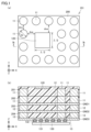
- FIG. 1 shows an antenna module 101 according to Embodiment 1.
- FIG. 1 the upper part (FIG. 1(a)) is a perspective plan view of the antenna module 101
- the lower part (FIG. 1(b)) is a perspective cross-sectional view of the antenna module 101.
- the positive direction of the Z-axis in FIG. 1 may be called the upper surface side
- the negative direction thereof may be called the lower surface side.
- the antenna module 101 includes a dielectric substrate 200 , a radiating element 120 and an RFIC (Radio Frequency Integrated Circuit) 130 .
- RFIC Radio Frequency Integrated Circuit
- the dielectric substrate 200 has a substantially rectangular shape when the antenna module 100 is viewed from above from the normal direction of the dielectric substrate 200 (the Z-axis direction in the drawing).
- Dielectric substrate 200 has, for example, a multilayer structure in which a plurality of dielectric layers are laminated.
- the dielectric substrate 200 is formed with dielectric layers including a first layer 201, a second layer 202, a third layer 203, and a fourth layer 204, as shown in FIG. 1(b).
- these layers may not necessarily be clearly visible after the dielectric substrate 200 is sintered through the process of laminating each layer.
- a radiating element 120 is arranged on the first layer 201 near one main surface (upper surface) of the dielectric substrate 200 .
- the radiating element 120 is composed of a flat patch antenna.
- the radiating element 120 is positioned in the first layer 201 on the side closer to the top surface of the dielectric substrate 200 .
- a radiating element 120 may be placed on the surface of the dielectric substrate 200 .
- the RFIC 130 is mounted on the other main surface (lower surface) of the dielectric substrate 200 .
- a plurality of copper posts 131 are formed on the surface of RFIC 130 .
- RFIC 130 is connected to ground electrode GND3 in dielectric substrate 200 by solder bumps 132 placed on respective copper posts 131 .
- the antenna module 101 requires measures to dissipate heat. Since the RFIC 130 is connected to the ground electrode GND3, it is conceivable that the ground electrode GND3 functions as a heat sink.
- ground electrodes GND1 to GND3 are provided along the layers of the dielectric substrate 200 and the ground electrodes GND1 to GND3 are connected by vias 11 to 13.
- FIG. The ground electrodes GND1 to GND3 and vias 11 to 13 correspond to conductors having a heat dissipation function, respectively.
- the arrangement of the ground electrodes GND1 to GND3 and the vias 11 to 13 is devised so that such a configuration does not adversely affect the antenna characteristics of the antenna module 101.
- the present embodiment will be described below including this point.
- a plurality of ground electrodes GND1 to GND3 are arranged in the direction in which the layers of the dielectric substrate 200 are formed.
- FIG. 1B shows an example in which the ground electrode GND1 is arranged on the second layer 202, the ground electrode GND2 is arranged on the third layer 203, and the ground electrode GND3 is arranged on the fourth layer 204. .
- Each of the ground electrodes GND1 to GND3 is composed of a solid ground that covers a wide range of the surface of the layers of the dielectric substrate 200 arranged thereon. By adopting the solid ground, the heat dissipation effect can be enhanced.
- a ground electrode is not arranged on the first layer 201 . From the viewpoint of enhancing the heat radiation effect, it is effective to arrange more ground electrodes functioning as heat radiation plates. However, since the radiating element 120 is arranged on the first layer 201 , the ground electrode arranged on the first layer 201 may adversely affect the antenna characteristics of the radiating element 120 .
- no ground electrode is arranged on the first layer 201 corresponding to the position near the radiating element 120 .
- the dielectric substrate 200 does not necessarily have a multi-layer structure, and may be a single-layer substrate. In that case, one ground electrode formed of solid ground may be arranged on the dielectric substrate 200 .
- a dielectric substrate 200 is formed with a plurality of vias 11-13.
- the plurality of vias 11 to 13 are formed parallel to the normal direction when the antenna module 101 is viewed from the normal direction.
- the via 11 penetrates between the first layer 201 and the second layer 202 and is arranged between the ground electrode GND1 and the radiating element 120 .
- the via 12 is arranged between the ground electrode GND1 and the ground electrode GND2.
- the via 13 is arranged between the ground electrode GND2 and the ground electrode GND3.
- the vias 11 to 13 are filled with a conductive member such as copper.
- One end of both ends of the via 11 is connected to the ground electrode GND1.
- the other end of via 11 extends up into first layer 201 of dielectric substrate 200 .
- the other end of the via 11 may reach the position of the radiating element 120 in the Z-axis direction, as shown in the cross-sectional view. Also, the other end of the via 11 may be fixed below the position of the radiating element 120 in the Z-axis direction.
- One end of both ends of the via 12 is connected to the ground electrode GND1.
- the other end of via 12 is connected to ground electrode GND2.
- One end of both ends of via 13 is connected to ground electrode GND2.
- the other end of via 13 is connected to ground electrode GND3.
- Vias 11-13 are electrically connected to ground electrodes GND1-GND3. Therefore, the vias 11 to 13, like the ground electrodes GND1 to GND3, exhibit a heat dissipation function of releasing heat generated by the RFIC 130.
- the plurality of vias 11 are formed so that the corresponding vias 12 and via holes overlap when the antenna module 101 is viewed from the normal direction.
- the plurality of vias 12 are formed so that the corresponding vias 13 and via holes overlap when the antenna module 101 is viewed from the normal direction.
- FIG. 1(a) is a diagram showing the radiating element 120 and the plurality of vias 11 with respect to the dielectric substrate 200. FIG. Therefore, only the radiating element 120 and the plurality of vias 11 in the dielectric substrate 200 are shown in FIG. 1(a).
- the dielectric substrate 200 is provided with a plurality of vias 11 surrounding the radiating element 120. As shown in FIG. Each of the plurality of vias 11 is connected to vias 12 and 13 via ground electrodes GND1 and GND2, as shown in FIG. 1(b). Note that the vias 11 to 13 may be arranged in a number exceeding the number shown in FIG. 1(a) in each of the X-axis direction and the Y-axis direction.
- the vias 11 to 13 can prevent electromagnetic waves radiated from the power amplifier or the like included in the RFIC 130 from reaching the radiating element 120 . As a result, the generation of noise in the radiating element 120 can be suppressed.
- via 11 is formed including first layer 201 .
- the arrangement of the vias 11 is devised so as not to adversely affect the antenna characteristics.
- the vias 11 to 13 correspond to columnar conductors each having a heat dissipation function.
- the radiating element 120 and the RFIC 130 are electrically connected via a feeder line (not shown). Feed lines pass through vias 11 - 13 and are connected to feed points of radiating element 120 .
- the feeding point is arranged in the radiating element 120 at a position offset from the center of the radiating element 120 toward one of the two sides parallel to the Y-axis. Therefore, radio waves are radiated from the radiating element 120 with the X-axis direction as the polarization direction.
- the feeding point may be arranged at a position offset from the center of the radiating element 120 toward one of the two sides parallel to the X-axis. In this case, the radiation element 120 radiates radio waves whose polarization direction is the Y-axis direction.
- the feeding point may be arranged on a line passing through the center of the radiating element 120 and intersecting the X-axis and the Y-axis.
- radio waves are radiated with the polarization direction intersecting the X-axis and the Y-axis.
- ⁇ be the wavelength of the radio wave radiated from the radiation element 120 .
- ⁇ means, for example, the wavelength of radio waves reflecting the effective dielectric constant of the dielectric substrate 200 .
- the vertical and horizontal lengths of the radiation element 120 are ⁇ /2.
- dv be the diameter of the via 11 .
- dvc be the interval between adjacent vias 11 , 11 .
- dva be the distance between the via 11 and the radiating element 120 .
- the relationship between each value and the wavelength ⁇ is as follows.
- Diameter dv of via 11 dv ⁇ /2 Distance dvc between adjacent vias 11, 11: ⁇ /4 ⁇ dvc ⁇ /2 Distance dva between via 11 and radiating element 120: dva ⁇ /4
- the reason why the diameter dv of the via 11 is limited to ⁇ /2 or less is that if the diameter dv of the via 11 exceeds ⁇ /2, the radiating element 120 and the via 111 are likely to be coupled, which may adversely affect the antenna characteristics. It's for.
- the reason why the distance dva between the via 11 and the radiating element 120 is set to ⁇ /4 or more is that if the distance between the via 11 and the radiating element 120 is too short, the via 11 and the radiating element 120 are likely to be impedance-coupled, and the antenna is damaged. This is because it may adversely affect the matching characteristics.
- Diameter dv of via 11 dv ⁇ L Distance dvc between adjacent vias 11, 11: L/2 ⁇ dvc ⁇ L Distance dva between via 11 and radiating element 120: dva ⁇ L
- a plurality of ground electrodes GND1 to GND3 and vias 11 to 13 are employed in order to improve the heat radiation performance, and their arrangement is devised from the viewpoint of antenna performance.
- a large number of ground electrodes GND1 to GND3 functioning as a heat dissipation plate are adopted to ensure a larger heat dissipation area and, in consideration of the antenna performance, the first electrodes close to the radiating element 120 are arranged.
- Layer 201 is not provided with a ground electrode.
- a via 11 extending from the ground electrode GND1 to the first layer 201 is arranged for one purpose of enhancing the heat radiation effect.
- the arrangement of the vias 11 is devised as described with reference to FIG. 1(a).
- the via 11 is formed including a first layer 201 that avoids arranging a ground electrode so as not to adversely affect antenna characteristics. Therefore, by using the vias 11, the first layer 201 can be effectively utilized as a region for imparting heat dissipation performance.
- an antenna module capable of exhibiting a heat dissipation effect using a ground electrode while considering antenna characteristics.
- RFIC 130 may be placed inside the dielectric substrate 200 .
- RFIC 130 may be placed on ground electrode GND3 via copper post 131 and solder bump 132 .
- FIG. 1 shows an example in which all of the plurality of vias 11 to 13 forming the columnar conductors are accommodated inside the dielectric substrate 200 when the antenna module 101 is viewed from the normal direction.
- the vias 11 to 13 may be arranged so that the cross sections of the vias 11 to 13 constituting the columnar conductors are exposed on the side surface of the dielectric substrate 200 .
- FIG. 1 shows an example in which the radiation element 120, the vias 11 to 13, and the ground electrodes GND1 to GND3 are provided on the first layer 201 to the fourth layer 204 of one dielectric substrate 200.
- the antenna module may be constructed by constructing the parts from different substrates and electrically connecting both substrates with solder bumps.
- the first to third layers 201 to 203 of the dielectric substrate 200 and the fourth layer 204 of the dielectric substrate 200 are formed of different substrates, and the substrates are electrically connected by solder bumps.
- an antenna module may be constructed.
- FIG. 2 is a diagram showing antenna module 102 according to the second embodiment. Pads 20 are provided in vias 11 in antenna module 102 according to the second embodiment. In this respect, antenna module 102 according to the second embodiment differs from antenna module 101 according to the first embodiment.
- the pads 20 are provided at the ends of the vias 11 near the top surface of the dielectric substrate 200 and at the boundary between the first layer 201 and the second layer 202 through which the vias 11 penetrate.
- the antenna module 102 can further enhance the heat dissipation effect.
- the pad 20 surrounds the radiating element 120 instead of the via 11 shown in FIG. 1(a).
- the limitation on the diameter of the via 11, the limitation on the interval between the adjacent vias 11 and 11, and the limitation on the interval between the via 11 and the radiating element 120 described as the first embodiment are related to the diameter of the pad 20.
- the limitations are read as limitations, limitations on the spacing between adjacent pads 20 , 20 , and limitations on spacing between the pad 20 and the radiating element 120 .
- FIG. 3 is a diagram showing antenna module 103 according to the third embodiment.
- Antenna module 103 according to the third embodiment is obtained by removing pad 20 from antenna module 102 according to the second embodiment at the end of via 11 closer to the upper surface of dielectric substrate 200 .
- the configuration can be simplified.
- the size of the pads 20 used in the antenna module 103 and the size of the pads 20 used in the antenna module 102 may be different.
- the size of pad 20 employed in antenna module 103 may be larger than that of pad 20 employed in antenna module 102 .
- FIG. 4 is a diagram showing antenna module 104 according to the fourth embodiment. 4, the upper part (FIG. 4A) is a perspective plan view of the antenna module 104, and the lower part (FIG. 4B) is a perspective cross-sectional view of the antenna module 104. As shown in FIG. 4A, the upper part (FIG. 4A) is a perspective plan view of the antenna module 104, and the lower part (FIG. 4B) is a perspective cross-sectional view of the antenna module 104. As shown in FIG.
- Antenna module 104 according to the fourth embodiment has fewer vias 11 than antenna module 101 according to the first embodiment.
- the antenna module 104 is provided with a plurality of vias 11 along one of the four sides of the radiating element 120, and vias 11 along the other three sides. can't
- FIG. 4 shows an example in which two vias 11 are provided along one of the four sides of the radiating element 120 . More specifically, one of the two vias 11 is located near one of the four sides of the radiating element 120, and the other is located at one vertex of the radiating element 120 and one vertex of the dielectric substrate 200. is provided between
- the configuration of layers below the ground electrode GND1 of the dielectric substrate 200 of the antenna module 104 is the same as that of the antenna module 101 described as the first embodiment. Therefore, the antenna module 104 has many vias 12 and 13 in a layer below the ground electrode GND1 of the dielectric substrate 200 .
- the antenna module 104 by reducing the number of vias 11 provided near the radiating element 120, the influence of the vias 11 on the antenna characteristics can be reduced as much as possible.
- the number of vias 12 and 13 provided in a layer below the ground electrode GND1 of the dielectric substrate 200 may be larger than that of the antenna module 103. At least some of the vias 12 arranged at positions where the corresponding vias 11 are not formed in the Z-axis direction may not reach the ground electrode GND1.
- FIG. 5 is a diagram showing antenna module 105 according to the fifth embodiment.
- Antenna module 105 according to the fifth embodiment comprises multiple radiating elements 120 .
- FIG. 5 shows an example in which four radiating elements 120 are arrayed in a matrix of two rows and two columns.
- a rectangle R1 is formed by four radiating elements 120 arranged in an array.
- antenna module 105 in antenna module 105 according to Embodiment 5, a plurality of vias 11 are provided along two of the four sides of rectangle R1 formed by four radiating elements 120 .
- antenna module 105 includes RFIC 130, ground electrodes GND1 to GND3, vias 12 and 13, and the like. Furthermore, the configuration of layers below the ground electrode GND1 of the dielectric substrate 200 of the antenna module 105 is the same as that of the antenna module 101 described as the first embodiment. Therefore, the antenna module 105 has many vias 12 and 13 in a layer below the ground electrode GND1 of the dielectric substrate 200 .
- pads 20 may be provided in vias 11, as in antenna module 102 according to the second embodiment.
- a large number of vias 11 may be arranged in the antenna module 105 so as to surround the rectangle R1 formed by the four radiating elements 120 . However, no vias 11 are arranged within the rectangle R1, that is, between the adjacent radiating elements 120,120.
- pads 20 may be provided in the vias 11 similarly to the antenna module 102 or the antenna module 103 .
- FIG. 6 is a diagram showing antenna module 106 according to the sixth embodiment.
- Antenna module 106 according to the sixth embodiment comprises a plurality of radiating elements 120, similar to antenna module 105 according to the fifth embodiment.
- Antenna module 106 according to the sixth embodiment differs from antenna module 105 according to the fifth embodiment in that vias 11 are also arranged between adjacent radiating elements 120 , 120 .
- the vias 11 are arranged along at least one side of each radiating element 120 .
- antenna module 106 includes RFIC 130, ground electrodes GND1 to GND3, vias 12 and 13, and the like. Furthermore, the configuration of layers below the ground electrode GND1 of the dielectric substrate 200 of the antenna module 106 is the same as that of the antenna module 101 described as the first embodiment. Therefore, the antenna module 106 has a large number of vias 12 and 13 below the ground electrode GND1 of the dielectric substrate 200 .
- FIG. 6 shows an example in which vias 11 are arranged so as to surround two of four radiating elements 120 .
- vias 11 may be arranged to surround each of the four radiating elements 120 .
- pads 20 may be provided in the vias 11 similarly to the antenna module 102 or the antenna module 103 .
- FIG. 7 is a diagram showing antenna module 107 according to the seventh embodiment.
- radiating element 120 is provided inside dielectric substrate 200 in the Z-axis direction more than antenna module 101 according to the first embodiment.
- FIG. 7 shows an example in which the radiating element 120 is provided near the boundary between the first layer 201 and the second layer 202 .
- antenna module 107 In antenna module 107 according to the seventh embodiment, the end of via 11 closer to the upper surface of dielectric substrate 200 is positioned at the boundary between first layer 201 and second layer 202 . Therefore, the length of via 11 in the Z-axis direction is shorter than via 11 of antenna module 101 according to the first embodiment.
- the length of the via 11 in the Z-axis direction may be extended in the direction toward the upper surface of the dielectric substrate 200 .
- the position of one end of the via 11 may be higher than the position of the radiating element 120 in the Z-axis direction.
- the heat dissipation area can be increased.
- the heat dissipation performance can be further enhanced.
- FIG. 8 is a diagram showing antenna module 108 according to the eighth embodiment.
- antenna module 108 according to the eighth embodiment some vias 11 among a plurality of vias 11 are formed to be shifted in the X-axis direction at the boundary between first layer 201 and second layer 202 .
- the displaced portions are connected by wiring 30 .
- the pads 20 may be adopted.
- FIG. 9 is a diagram showing antenna module 109 according to the ninth embodiment.
- the thickness of some vias 11 among the plurality of vias 11 differs between first layer 201 and second layer 202 . Portions of the via 11 having different thicknesses are connected by pads 20 .
- the thickness of the via 11 is partially changed.
- the limitations on the diameter of the via 11, the limitations on the spacing between the adjacent vias 11 and 11, and the limitations on the spacing between the via 11 and the radiating element 120 described in the first embodiment also apply to the ninth embodiment. Apply.
- the diameter of the thickest via 11 is set to 1/2 or less of the wavelength ⁇ of the radio waves radiated from the radiating element 120 .
- FIG. 9 shows an example in which the thickness of the via 11 is made different between the first layer 201 and the second layer 202 .
- a plurality of pads 20 are provided as in the second embodiment in addition to the vias 11, even if the plurality of pads 20 include several types of pads 20 having different lengths in the X-axis direction, good.
- FIG. 10 shows antenna module 110 according to the tenth embodiment.
- pad 20 provided in via 11 is commonly used for a plurality of vias 11 .
- multiple vias 11 are connected by one pad 20 .
- FIG. 10 shows an example in which two vias 11 are connected by one pad 20 near the boundary between the first layer 201 and the second layer 202 .
- the length of one pad 20 in the X-axis direction can be increased, for example, compared to FIG. 3 used for explaining the third embodiment. Thereby, a larger heat dissipation area can be secured. As a result, heat dissipation performance can be improved.
- the tenth embodiment can also be applied to the configuration shown in FIG. However, it is desirable to apply the tenth embodiment except for the pads 20 existing near the upper surface of the dielectric substrate 200 among the plurality of pads 20 shown in FIG. This is because the radiating element 120 exists near the upper surface of the dielectric substrate 200 as shown in FIG.
- connecting two pads 20 near the upper surface of the dielectric substrate 200 increases the area of the pads 20 in the X-axis direction and the Y-axis direction. As a result, the performance of the pad 20 exhibiting a heat dissipation function is enhanced.
- the diameter of the pad 20, etc. must satisfy certain conditions in relation to the wavelength ⁇ of the radio waves radiated from the radiating element 120. There is If the two pads 20 existing near the upper surface of the dielectric substrate 200 are connected, the area of the pads 20 may become too large to satisfy the condition.
Landscapes
- Physics & Mathematics (AREA)
- Condensed Matter Physics & Semiconductors (AREA)
- General Physics & Mathematics (AREA)
- Engineering & Computer Science (AREA)
- Computer Hardware Design (AREA)
- Microelectronics & Electronic Packaging (AREA)
- Power Engineering (AREA)
- Waveguide Aerials (AREA)
Abstract
L'invention concerne un module d'antenne (101) comprenant un substrat diélectrique (200), un élément rayonnant (120), Une électrode de masse (GND1) électriquement connectée à un circuit haute fréquence et disposée à l'opposé de l'élément rayonnant (120), et une pluralité de trous d'interconnexion (11). Vu dans un plan à partir d'une direction perpendiculaire à l'élément rayonnant (120), la pluralité de trous d'interconnexion (11) sont disposés dans des positions ne chevauchant pas l'élément rayonnant (120). L'intervalle entre deux trous d'interconnexion adjacents (11, 11) est inférieur ou égal à la longueur de l'élément rayonnant (120) dans une direction passant à travers le centre de l'élément rayonnant (120) et orthogonal à la direction normale.
Applications Claiming Priority (2)
| Application Number | Priority Date | Filing Date | Title |
|---|---|---|---|
| JP2021-135786 | 2021-08-23 | ||
| JP2021135786 | 2021-08-23 |
Publications (1)
| Publication Number | Publication Date |
|---|---|
| WO2023026848A1 true WO2023026848A1 (fr) | 2023-03-02 |
Family
ID=85323154
Family Applications (1)
| Application Number | Title | Priority Date | Filing Date |
|---|---|---|---|
| PCT/JP2022/030405 WO2023026848A1 (fr) | 2021-08-23 | 2022-08-09 | Module d'antenne |
Country Status (1)
| Country | Link |
|---|---|
| WO (1) | WO2023026848A1 (fr) |
Citations (5)
| Publication number | Priority date | Publication date | Assignee | Title |
|---|---|---|---|---|
| JP2005191435A (ja) * | 2003-12-26 | 2005-07-14 | Tdk Corp | 放熱ビア付き基板およびパワーアンプモジュール |
| US20100327068A1 (en) * | 2009-06-30 | 2010-12-30 | International Business Machines Corporation | Compact millimeter wave packages with integrated antennas |
| JP2012089590A (ja) * | 2010-10-18 | 2012-05-10 | Hitachi Metals Ltd | 電子部品 |
| JP2015015274A (ja) * | 2013-07-03 | 2015-01-22 | 三菱電機株式会社 | 電力用半導体装置 |
| JP2019068040A (ja) * | 2017-09-30 | 2019-04-25 | インテル・コーポレーション | 埋め込みダイパッケージの熱性能を向上させるための新規なアーキテクチャ材料および処理 |
-
2022
- 2022-08-09 WO PCT/JP2022/030405 patent/WO2023026848A1/fr unknown
Patent Citations (5)
| Publication number | Priority date | Publication date | Assignee | Title |
|---|---|---|---|---|
| JP2005191435A (ja) * | 2003-12-26 | 2005-07-14 | Tdk Corp | 放熱ビア付き基板およびパワーアンプモジュール |
| US20100327068A1 (en) * | 2009-06-30 | 2010-12-30 | International Business Machines Corporation | Compact millimeter wave packages with integrated antennas |
| JP2012089590A (ja) * | 2010-10-18 | 2012-05-10 | Hitachi Metals Ltd | 電子部品 |
| JP2015015274A (ja) * | 2013-07-03 | 2015-01-22 | 三菱電機株式会社 | 電力用半導体装置 |
| JP2019068040A (ja) * | 2017-09-30 | 2019-04-25 | インテル・コーポレーション | 埋め込みダイパッケージの熱性能を向上させるための新規なアーキテクチャ材料および処理 |
Similar Documents
| Publication | Publication Date | Title |
|---|---|---|
| US9985346B2 (en) | Wireless communications package with integrated antennas and air cavity | |
| JP6821008B2 (ja) | マイクロ波デバイス及び空中線 | |
| US11602089B2 (en) | High-frequency module | |
| US9648794B2 (en) | Wiring board and electronic apparatus | |
| US10439264B2 (en) | Wireless device | |
| US11611146B2 (en) | Antenna array radiation shielding | |
| US8735945B2 (en) | Semiconductor device | |
| JP2005026263A (ja) | 混成集積回路 | |
| TW201842712A (zh) | 高頻模組 | |
| JPWO2020100849A1 (ja) | 実装型電子部品、および、電子回路モジュール | |
| JP5354394B2 (ja) | 部品内蔵基板及びその製造方法 | |
| WO2023026848A1 (fr) | Module d'antenne | |
| TWI567905B (zh) | 半導體裝置 | |
| US9691722B2 (en) | Surface mount high-frequency circuit | |
| JP7130470B2 (ja) | 無線通信装置 | |
| JP7005111B2 (ja) | 電子部品実装品 | |
| US8520354B2 (en) | Multilayered board semiconductor device with BGA package | |
| US20220192026A1 (en) | Electronic component module | |
| US20220384943A1 (en) | Grounding assembly for a semiconductor device | |
| JP7433555B2 (ja) | アンテナ装置及びアンテナ装置の製造方法 | |
| US11862874B2 (en) | Antenna structure and antenna-in-package | |
| KR101305581B1 (ko) | 차폐 부재 및 이를 포함하는 인쇄회로기판 | |
| JP7192970B2 (ja) | 電子部品モジュール | |
| US20240014121A1 (en) | Electronic circuit module | |
| JPWO2022185874A5 (fr) |
Legal Events
| Date | Code | Title | Description |
|---|---|---|---|
| 121 | Ep: the epo has been informed by wipo that ep was designated in this application |
Ref document number: 22861138 Country of ref document: EP Kind code of ref document: A1 |
|
| NENP | Non-entry into the national phase |
Ref country code: DE |