WO2023026848A1 - Antenna module - Google Patents
Antenna module Download PDFInfo
- Publication number
- WO2023026848A1 WO2023026848A1 PCT/JP2022/030405 JP2022030405W WO2023026848A1 WO 2023026848 A1 WO2023026848 A1 WO 2023026848A1 JP 2022030405 W JP2022030405 W JP 2022030405W WO 2023026848 A1 WO2023026848 A1 WO 2023026848A1
- Authority
- WO
- WIPO (PCT)
- Prior art keywords
- radiating element
- antenna module
- ground electrode
- vias
- columnar conductors
- Prior art date
Links
Images


Classifications
-
- H—ELECTRICITY
- H01—ELECTRIC ELEMENTS
- H01L—SEMICONDUCTOR DEVICES NOT COVERED BY CLASS H10
- H01L23/00—Details of semiconductor or other solid state devices
- H01L23/12—Mountings, e.g. non-detachable insulating substrates
-
- H—ELECTRICITY
- H01—ELECTRIC ELEMENTS
- H01P—WAVEGUIDES; RESONATORS, LINES, OR OTHER DEVICES OF THE WAVEGUIDE TYPE
- H01P1/00—Auxiliary devices
- H01P1/30—Auxiliary devices for compensation of, or protection against, temperature or moisture effects ; for improving power handling capability
-
- H—ELECTRICITY
- H01—ELECTRIC ELEMENTS
- H01Q—ANTENNAS, i.e. RADIO AERIALS
- H01Q23/00—Antennas with active circuits or circuit elements integrated within them or attached to them
Definitions
- the present disclosure relates to antenna modules, and more particularly to antenna modules having planar radiating elements.
- Patent Document 1 a flat patch antenna (radiating element) is arranged near one surface of a rectangular dielectric substrate, and a high frequency integrated circuit is arranged on the other surface.
- An antenna module is disclosed.
- radio waves are radiated from the radiating element due to electromagnetic field coupling between the radiating element and the ground electrode arranged opposite to it.
- high-frequency integrated circuits have heat sources such as power amplifiers, so heat dissipation measures are required for antenna modules.
- heat sources such as power amplifiers
- heat dissipation measures are required for antenna modules.
- increasing the surface area of the ground electrode disposed within the antenna module is considered effective for heat dissipation. This is because a large amount of heat can escape from the surface of the ground electrode.
- the ground electrode is a type of conductor, the shape and position of the ground electrode affect the antenna characteristics of the radiating element. Therefore, there is a demand for an antenna module that can exhibit a heat dissipation effect using a ground electrode while taking into consideration the antenna characteristics of the radiating element.
- the present disclosure has been made to solve such problems, and an object thereof is to provide an antenna module that can exert a heat dissipation effect by using a ground electrode while considering antenna characteristics. .
- An antenna module is electrically connected to a dielectric substrate, at least one planar radiation element disposed on the dielectric substrate, and a high-frequency circuit and disposed opposite the radiation element. and a plurality of columnar conductors electrically connected to the first ground electrode and arranged between the first ground electrode and the radiating element.
- the plurality of columnar conductors are viewed in plan from the normal direction of the radiating element, the plurality of columnar conductors are arranged at positions that do not overlap with the radiating element, and among the plurality of columnar conductors, two adjacent columnar conductors are separated from each other.
- the spacing is the length of the radiating element in a direction perpendicular to the normal direction through the center of the radiating element.
- An antenna module includes a dielectric substrate, at least one planar radiation element disposed on the dielectric substrate, and electrically connected to a high frequency circuit and disposed opposite the radiation element. and a plurality of columnar conductors electrically connected to the first ground electrode and arranged between the first ground electrode and the radiating element, wherein the wavelength of radio waves radiated from the radiating element is ⁇ . Then, when the radiating element is planarly viewed from the normal direction, the plurality of columnar conductors are arranged at positions that do not overlap with the radiating element, and among the plurality of columnar conductors, the distance between two adjacent columnar conductors is ⁇ /4 or more and ⁇ /2 or less.
- the antenna module according to the present disclosure it is possible to provide an antenna module capable of exhibiting a heat dissipation effect using a ground electrode while considering antenna characteristics.
- FIG. 1 shows an antenna module according to Embodiment 1;
- FIG. FIG. 4 shows an antenna module according to Embodiment 2;
- FIG. 11 shows an antenna module according to Embodiment 3;
- FIG. 11 shows an antenna module according to Embodiment 4;
- FIG. 11 shows an antenna module according to Embodiment 5;
- FIG. 11 shows an antenna module according to Embodiment 6;
- FIG. 11 shows an antenna module according to Embodiment 7;
- FIG. 11 shows an antenna module according to Embodiment 8;
- FIG. 21 shows an antenna module according to a ninth embodiment;
- FIG. 21 shows an antenna module according to Embodiment 10;
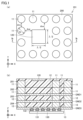
- FIG. 1 shows an antenna module 101 according to Embodiment 1.
- FIG. 1 the upper part (FIG. 1(a)) is a perspective plan view of the antenna module 101
- the lower part (FIG. 1(b)) is a perspective cross-sectional view of the antenna module 101.
- the positive direction of the Z-axis in FIG. 1 may be called the upper surface side
- the negative direction thereof may be called the lower surface side.
- the antenna module 101 includes a dielectric substrate 200 , a radiating element 120 and an RFIC (Radio Frequency Integrated Circuit) 130 .
- RFIC Radio Frequency Integrated Circuit
- the dielectric substrate 200 has a substantially rectangular shape when the antenna module 100 is viewed from above from the normal direction of the dielectric substrate 200 (the Z-axis direction in the drawing).
- Dielectric substrate 200 has, for example, a multilayer structure in which a plurality of dielectric layers are laminated.
- the dielectric substrate 200 is formed with dielectric layers including a first layer 201, a second layer 202, a third layer 203, and a fourth layer 204, as shown in FIG. 1(b).
- these layers may not necessarily be clearly visible after the dielectric substrate 200 is sintered through the process of laminating each layer.
- a radiating element 120 is arranged on the first layer 201 near one main surface (upper surface) of the dielectric substrate 200 .
- the radiating element 120 is composed of a flat patch antenna.
- the radiating element 120 is positioned in the first layer 201 on the side closer to the top surface of the dielectric substrate 200 .
- a radiating element 120 may be placed on the surface of the dielectric substrate 200 .
- the RFIC 130 is mounted on the other main surface (lower surface) of the dielectric substrate 200 .
- a plurality of copper posts 131 are formed on the surface of RFIC 130 .
- RFIC 130 is connected to ground electrode GND3 in dielectric substrate 200 by solder bumps 132 placed on respective copper posts 131 .
- the antenna module 101 requires measures to dissipate heat. Since the RFIC 130 is connected to the ground electrode GND3, it is conceivable that the ground electrode GND3 functions as a heat sink.
- ground electrodes GND1 to GND3 are provided along the layers of the dielectric substrate 200 and the ground electrodes GND1 to GND3 are connected by vias 11 to 13.
- FIG. The ground electrodes GND1 to GND3 and vias 11 to 13 correspond to conductors having a heat dissipation function, respectively.
- the arrangement of the ground electrodes GND1 to GND3 and the vias 11 to 13 is devised so that such a configuration does not adversely affect the antenna characteristics of the antenna module 101.
- the present embodiment will be described below including this point.
- a plurality of ground electrodes GND1 to GND3 are arranged in the direction in which the layers of the dielectric substrate 200 are formed.
- FIG. 1B shows an example in which the ground electrode GND1 is arranged on the second layer 202, the ground electrode GND2 is arranged on the third layer 203, and the ground electrode GND3 is arranged on the fourth layer 204. .
- Each of the ground electrodes GND1 to GND3 is composed of a solid ground that covers a wide range of the surface of the layers of the dielectric substrate 200 arranged thereon. By adopting the solid ground, the heat dissipation effect can be enhanced.
- a ground electrode is not arranged on the first layer 201 . From the viewpoint of enhancing the heat radiation effect, it is effective to arrange more ground electrodes functioning as heat radiation plates. However, since the radiating element 120 is arranged on the first layer 201 , the ground electrode arranged on the first layer 201 may adversely affect the antenna characteristics of the radiating element 120 .
- no ground electrode is arranged on the first layer 201 corresponding to the position near the radiating element 120 .
- the dielectric substrate 200 does not necessarily have a multi-layer structure, and may be a single-layer substrate. In that case, one ground electrode formed of solid ground may be arranged on the dielectric substrate 200 .
- a dielectric substrate 200 is formed with a plurality of vias 11-13.
- the plurality of vias 11 to 13 are formed parallel to the normal direction when the antenna module 101 is viewed from the normal direction.
- the via 11 penetrates between the first layer 201 and the second layer 202 and is arranged between the ground electrode GND1 and the radiating element 120 .
- the via 12 is arranged between the ground electrode GND1 and the ground electrode GND2.
- the via 13 is arranged between the ground electrode GND2 and the ground electrode GND3.
- the vias 11 to 13 are filled with a conductive member such as copper.
- One end of both ends of the via 11 is connected to the ground electrode GND1.
- the other end of via 11 extends up into first layer 201 of dielectric substrate 200 .
- the other end of the via 11 may reach the position of the radiating element 120 in the Z-axis direction, as shown in the cross-sectional view. Also, the other end of the via 11 may be fixed below the position of the radiating element 120 in the Z-axis direction.
- One end of both ends of the via 12 is connected to the ground electrode GND1.
- the other end of via 12 is connected to ground electrode GND2.
- One end of both ends of via 13 is connected to ground electrode GND2.
- the other end of via 13 is connected to ground electrode GND3.
- Vias 11-13 are electrically connected to ground electrodes GND1-GND3. Therefore, the vias 11 to 13, like the ground electrodes GND1 to GND3, exhibit a heat dissipation function of releasing heat generated by the RFIC 130.
- the plurality of vias 11 are formed so that the corresponding vias 12 and via holes overlap when the antenna module 101 is viewed from the normal direction.
- the plurality of vias 12 are formed so that the corresponding vias 13 and via holes overlap when the antenna module 101 is viewed from the normal direction.
- FIG. 1(a) is a diagram showing the radiating element 120 and the plurality of vias 11 with respect to the dielectric substrate 200. FIG. Therefore, only the radiating element 120 and the plurality of vias 11 in the dielectric substrate 200 are shown in FIG. 1(a).
- the dielectric substrate 200 is provided with a plurality of vias 11 surrounding the radiating element 120. As shown in FIG. Each of the plurality of vias 11 is connected to vias 12 and 13 via ground electrodes GND1 and GND2, as shown in FIG. 1(b). Note that the vias 11 to 13 may be arranged in a number exceeding the number shown in FIG. 1(a) in each of the X-axis direction and the Y-axis direction.
- the vias 11 to 13 can prevent electromagnetic waves radiated from the power amplifier or the like included in the RFIC 130 from reaching the radiating element 120 . As a result, the generation of noise in the radiating element 120 can be suppressed.
- via 11 is formed including first layer 201 .
- the arrangement of the vias 11 is devised so as not to adversely affect the antenna characteristics.
- the vias 11 to 13 correspond to columnar conductors each having a heat dissipation function.
- the radiating element 120 and the RFIC 130 are electrically connected via a feeder line (not shown). Feed lines pass through vias 11 - 13 and are connected to feed points of radiating element 120 .
- the feeding point is arranged in the radiating element 120 at a position offset from the center of the radiating element 120 toward one of the two sides parallel to the Y-axis. Therefore, radio waves are radiated from the radiating element 120 with the X-axis direction as the polarization direction.
- the feeding point may be arranged at a position offset from the center of the radiating element 120 toward one of the two sides parallel to the X-axis. In this case, the radiation element 120 radiates radio waves whose polarization direction is the Y-axis direction.
- the feeding point may be arranged on a line passing through the center of the radiating element 120 and intersecting the X-axis and the Y-axis.
- radio waves are radiated with the polarization direction intersecting the X-axis and the Y-axis.
- ⁇ be the wavelength of the radio wave radiated from the radiation element 120 .
- ⁇ means, for example, the wavelength of radio waves reflecting the effective dielectric constant of the dielectric substrate 200 .
- the vertical and horizontal lengths of the radiation element 120 are ⁇ /2.
- dv be the diameter of the via 11 .
- dvc be the interval between adjacent vias 11 , 11 .
- dva be the distance between the via 11 and the radiating element 120 .
- the relationship between each value and the wavelength ⁇ is as follows.
- Diameter dv of via 11 dv ⁇ /2 Distance dvc between adjacent vias 11, 11: ⁇ /4 ⁇ dvc ⁇ /2 Distance dva between via 11 and radiating element 120: dva ⁇ /4
- the reason why the diameter dv of the via 11 is limited to ⁇ /2 or less is that if the diameter dv of the via 11 exceeds ⁇ /2, the radiating element 120 and the via 111 are likely to be coupled, which may adversely affect the antenna characteristics. It's for.
- the reason why the distance dva between the via 11 and the radiating element 120 is set to ⁇ /4 or more is that if the distance between the via 11 and the radiating element 120 is too short, the via 11 and the radiating element 120 are likely to be impedance-coupled, and the antenna is damaged. This is because it may adversely affect the matching characteristics.
- Diameter dv of via 11 dv ⁇ L Distance dvc between adjacent vias 11, 11: L/2 ⁇ dvc ⁇ L Distance dva between via 11 and radiating element 120: dva ⁇ L
- a plurality of ground electrodes GND1 to GND3 and vias 11 to 13 are employed in order to improve the heat radiation performance, and their arrangement is devised from the viewpoint of antenna performance.
- a large number of ground electrodes GND1 to GND3 functioning as a heat dissipation plate are adopted to ensure a larger heat dissipation area and, in consideration of the antenna performance, the first electrodes close to the radiating element 120 are arranged.
- Layer 201 is not provided with a ground electrode.
- a via 11 extending from the ground electrode GND1 to the first layer 201 is arranged for one purpose of enhancing the heat radiation effect.
- the arrangement of the vias 11 is devised as described with reference to FIG. 1(a).
- the via 11 is formed including a first layer 201 that avoids arranging a ground electrode so as not to adversely affect antenna characteristics. Therefore, by using the vias 11, the first layer 201 can be effectively utilized as a region for imparting heat dissipation performance.
- an antenna module capable of exhibiting a heat dissipation effect using a ground electrode while considering antenna characteristics.
- RFIC 130 may be placed inside the dielectric substrate 200 .
- RFIC 130 may be placed on ground electrode GND3 via copper post 131 and solder bump 132 .
- FIG. 1 shows an example in which all of the plurality of vias 11 to 13 forming the columnar conductors are accommodated inside the dielectric substrate 200 when the antenna module 101 is viewed from the normal direction.
- the vias 11 to 13 may be arranged so that the cross sections of the vias 11 to 13 constituting the columnar conductors are exposed on the side surface of the dielectric substrate 200 .
- FIG. 1 shows an example in which the radiation element 120, the vias 11 to 13, and the ground electrodes GND1 to GND3 are provided on the first layer 201 to the fourth layer 204 of one dielectric substrate 200.
- the antenna module may be constructed by constructing the parts from different substrates and electrically connecting both substrates with solder bumps.
- the first to third layers 201 to 203 of the dielectric substrate 200 and the fourth layer 204 of the dielectric substrate 200 are formed of different substrates, and the substrates are electrically connected by solder bumps.
- an antenna module may be constructed.
- FIG. 2 is a diagram showing antenna module 102 according to the second embodiment. Pads 20 are provided in vias 11 in antenna module 102 according to the second embodiment. In this respect, antenna module 102 according to the second embodiment differs from antenna module 101 according to the first embodiment.
- the pads 20 are provided at the ends of the vias 11 near the top surface of the dielectric substrate 200 and at the boundary between the first layer 201 and the second layer 202 through which the vias 11 penetrate.
- the antenna module 102 can further enhance the heat dissipation effect.
- the pad 20 surrounds the radiating element 120 instead of the via 11 shown in FIG. 1(a).
- the limitation on the diameter of the via 11, the limitation on the interval between the adjacent vias 11 and 11, and the limitation on the interval between the via 11 and the radiating element 120 described as the first embodiment are related to the diameter of the pad 20.
- the limitations are read as limitations, limitations on the spacing between adjacent pads 20 , 20 , and limitations on spacing between the pad 20 and the radiating element 120 .
- FIG. 3 is a diagram showing antenna module 103 according to the third embodiment.
- Antenna module 103 according to the third embodiment is obtained by removing pad 20 from antenna module 102 according to the second embodiment at the end of via 11 closer to the upper surface of dielectric substrate 200 .
- the configuration can be simplified.
- the size of the pads 20 used in the antenna module 103 and the size of the pads 20 used in the antenna module 102 may be different.
- the size of pad 20 employed in antenna module 103 may be larger than that of pad 20 employed in antenna module 102 .
- FIG. 4 is a diagram showing antenna module 104 according to the fourth embodiment. 4, the upper part (FIG. 4A) is a perspective plan view of the antenna module 104, and the lower part (FIG. 4B) is a perspective cross-sectional view of the antenna module 104. As shown in FIG. 4A, the upper part (FIG. 4A) is a perspective plan view of the antenna module 104, and the lower part (FIG. 4B) is a perspective cross-sectional view of the antenna module 104. As shown in FIG.
- Antenna module 104 according to the fourth embodiment has fewer vias 11 than antenna module 101 according to the first embodiment.
- the antenna module 104 is provided with a plurality of vias 11 along one of the four sides of the radiating element 120, and vias 11 along the other three sides. can't
- FIG. 4 shows an example in which two vias 11 are provided along one of the four sides of the radiating element 120 . More specifically, one of the two vias 11 is located near one of the four sides of the radiating element 120, and the other is located at one vertex of the radiating element 120 and one vertex of the dielectric substrate 200. is provided between
- the configuration of layers below the ground electrode GND1 of the dielectric substrate 200 of the antenna module 104 is the same as that of the antenna module 101 described as the first embodiment. Therefore, the antenna module 104 has many vias 12 and 13 in a layer below the ground electrode GND1 of the dielectric substrate 200 .
- the antenna module 104 by reducing the number of vias 11 provided near the radiating element 120, the influence of the vias 11 on the antenna characteristics can be reduced as much as possible.
- the number of vias 12 and 13 provided in a layer below the ground electrode GND1 of the dielectric substrate 200 may be larger than that of the antenna module 103. At least some of the vias 12 arranged at positions where the corresponding vias 11 are not formed in the Z-axis direction may not reach the ground electrode GND1.
- FIG. 5 is a diagram showing antenna module 105 according to the fifth embodiment.
- Antenna module 105 according to the fifth embodiment comprises multiple radiating elements 120 .
- FIG. 5 shows an example in which four radiating elements 120 are arrayed in a matrix of two rows and two columns.
- a rectangle R1 is formed by four radiating elements 120 arranged in an array.
- antenna module 105 in antenna module 105 according to Embodiment 5, a plurality of vias 11 are provided along two of the four sides of rectangle R1 formed by four radiating elements 120 .
- antenna module 105 includes RFIC 130, ground electrodes GND1 to GND3, vias 12 and 13, and the like. Furthermore, the configuration of layers below the ground electrode GND1 of the dielectric substrate 200 of the antenna module 105 is the same as that of the antenna module 101 described as the first embodiment. Therefore, the antenna module 105 has many vias 12 and 13 in a layer below the ground electrode GND1 of the dielectric substrate 200 .
- pads 20 may be provided in vias 11, as in antenna module 102 according to the second embodiment.
- a large number of vias 11 may be arranged in the antenna module 105 so as to surround the rectangle R1 formed by the four radiating elements 120 . However, no vias 11 are arranged within the rectangle R1, that is, between the adjacent radiating elements 120,120.
- pads 20 may be provided in the vias 11 similarly to the antenna module 102 or the antenna module 103 .
- FIG. 6 is a diagram showing antenna module 106 according to the sixth embodiment.
- Antenna module 106 according to the sixth embodiment comprises a plurality of radiating elements 120, similar to antenna module 105 according to the fifth embodiment.
- Antenna module 106 according to the sixth embodiment differs from antenna module 105 according to the fifth embodiment in that vias 11 are also arranged between adjacent radiating elements 120 , 120 .
- the vias 11 are arranged along at least one side of each radiating element 120 .
- antenna module 106 includes RFIC 130, ground electrodes GND1 to GND3, vias 12 and 13, and the like. Furthermore, the configuration of layers below the ground electrode GND1 of the dielectric substrate 200 of the antenna module 106 is the same as that of the antenna module 101 described as the first embodiment. Therefore, the antenna module 106 has a large number of vias 12 and 13 below the ground electrode GND1 of the dielectric substrate 200 .
- FIG. 6 shows an example in which vias 11 are arranged so as to surround two of four radiating elements 120 .
- vias 11 may be arranged to surround each of the four radiating elements 120 .
- pads 20 may be provided in the vias 11 similarly to the antenna module 102 or the antenna module 103 .
- FIG. 7 is a diagram showing antenna module 107 according to the seventh embodiment.
- radiating element 120 is provided inside dielectric substrate 200 in the Z-axis direction more than antenna module 101 according to the first embodiment.
- FIG. 7 shows an example in which the radiating element 120 is provided near the boundary between the first layer 201 and the second layer 202 .
- antenna module 107 In antenna module 107 according to the seventh embodiment, the end of via 11 closer to the upper surface of dielectric substrate 200 is positioned at the boundary between first layer 201 and second layer 202 . Therefore, the length of via 11 in the Z-axis direction is shorter than via 11 of antenna module 101 according to the first embodiment.
- the length of the via 11 in the Z-axis direction may be extended in the direction toward the upper surface of the dielectric substrate 200 .
- the position of one end of the via 11 may be higher than the position of the radiating element 120 in the Z-axis direction.
- the heat dissipation area can be increased.
- the heat dissipation performance can be further enhanced.
- FIG. 8 is a diagram showing antenna module 108 according to the eighth embodiment.
- antenna module 108 according to the eighth embodiment some vias 11 among a plurality of vias 11 are formed to be shifted in the X-axis direction at the boundary between first layer 201 and second layer 202 .
- the displaced portions are connected by wiring 30 .
- the pads 20 may be adopted.
- FIG. 9 is a diagram showing antenna module 109 according to the ninth embodiment.
- the thickness of some vias 11 among the plurality of vias 11 differs between first layer 201 and second layer 202 . Portions of the via 11 having different thicknesses are connected by pads 20 .
- the thickness of the via 11 is partially changed.
- the limitations on the diameter of the via 11, the limitations on the spacing between the adjacent vias 11 and 11, and the limitations on the spacing between the via 11 and the radiating element 120 described in the first embodiment also apply to the ninth embodiment. Apply.
- the diameter of the thickest via 11 is set to 1/2 or less of the wavelength ⁇ of the radio waves radiated from the radiating element 120 .
- FIG. 9 shows an example in which the thickness of the via 11 is made different between the first layer 201 and the second layer 202 .
- a plurality of pads 20 are provided as in the second embodiment in addition to the vias 11, even if the plurality of pads 20 include several types of pads 20 having different lengths in the X-axis direction, good.
- FIG. 10 shows antenna module 110 according to the tenth embodiment.
- pad 20 provided in via 11 is commonly used for a plurality of vias 11 .
- multiple vias 11 are connected by one pad 20 .
- FIG. 10 shows an example in which two vias 11 are connected by one pad 20 near the boundary between the first layer 201 and the second layer 202 .
- the length of one pad 20 in the X-axis direction can be increased, for example, compared to FIG. 3 used for explaining the third embodiment. Thereby, a larger heat dissipation area can be secured. As a result, heat dissipation performance can be improved.
- the tenth embodiment can also be applied to the configuration shown in FIG. However, it is desirable to apply the tenth embodiment except for the pads 20 existing near the upper surface of the dielectric substrate 200 among the plurality of pads 20 shown in FIG. This is because the radiating element 120 exists near the upper surface of the dielectric substrate 200 as shown in FIG.
- connecting two pads 20 near the upper surface of the dielectric substrate 200 increases the area of the pads 20 in the X-axis direction and the Y-axis direction. As a result, the performance of the pad 20 exhibiting a heat dissipation function is enhanced.
- the diameter of the pad 20, etc. must satisfy certain conditions in relation to the wavelength ⁇ of the radio waves radiated from the radiating element 120. There is If the two pads 20 existing near the upper surface of the dielectric substrate 200 are connected, the area of the pads 20 may become too large to satisfy the condition.
Abstract
An antenna module (101) comprising a dielectric substrate (200), a radiating element (120), a ground electrode (GND1) electrically connected to a high frequency circuit and disposed opposite the radiating element (120), and a plurality of vias (11). When viewed in plan from a direction normal to the radiating element (120), the plurality of vias (11) are disposed in positions not overlapping the radiating element (120). The interval between two adjacent vias (11, 11) is less than or equal to the length of the radiating element (120) in a direction passing through the center of the radiating element (120) and orthogonal to the normal direction.
Description
本開示は、アンテナモジュールに関し、より特定的には、平板状の放射素子を有するアンテナモジュールに関する。
The present disclosure relates to antenna modules, and more particularly to antenna modules having planar radiating elements.
特開2021-016198号公報(特許文献1)には、矩形状の誘電体基板の一方の面の近傍に平板状のパッチアンテナ(放射素子)が配置され、他方の面に高周波集積回路が配置されたアンテナモジュールが開示されている。
In Japanese Patent Application Laid-Open No. 2021-016198 (Patent Document 1), a flat patch antenna (radiating element) is arranged near one surface of a rectangular dielectric substrate, and a high frequency integrated circuit is arranged on the other surface. An antenna module is disclosed.
このようなパッチアンテナを用いたアンテナモジュールにおいては、放射素子とそれに対向して配置された接地電極との間の電磁界結合により、放射素子から電波が放射される。
In an antenna module using such a patch antenna, radio waves are radiated from the radiating element due to electromagnetic field coupling between the radiating element and the ground electrode arranged opposite to it.
一般に、高周波集積回路は電力増幅器(Power Amplifier)などの発熱源を有するため、アンテナモジュールには放熱対策が必要とされる。たとえば、アンテナモジュール内に配置される接地電極の表面積を増大させることは、放熱対策に有効であると考えられる。接地電極の表面から多くの熱を逃がすことができるためである。
In general, high-frequency integrated circuits have heat sources such as power amplifiers, so heat dissipation measures are required for antenna modules. For example, increasing the surface area of the ground electrode disposed within the antenna module is considered effective for heat dissipation. This is because a large amount of heat can escape from the surface of the ground electrode.
しかしながら、接地電極は導体の一種であるため、接地電極の形状および位置は放射素子のアンテナ特性に影響を与える。したがって、放射素子のアンテナ特性を考慮しつつ、接地電極を利用した放熱効果を発揮できるアンテナモジュールが求められる。
However, since the ground electrode is a type of conductor, the shape and position of the ground electrode affect the antenna characteristics of the radiating element. Therefore, there is a demand for an antenna module that can exhibit a heat dissipation effect using a ground electrode while taking into consideration the antenna characteristics of the radiating element.
本開示は、このような課題を解決するためになされたものであって、その目的は、アンテナ特性を考慮しつつ、接地電極を利用して放熱効果を発揮できるアンテナモジュールを提供することである。
The present disclosure has been made to solve such problems, and an object thereof is to provide an antenna module that can exert a heat dissipation effect by using a ground electrode while considering antenna characteristics. .
本開示のある局面に従うアンテナモジュールは、誘電体基板と、誘電体基板に配置される、少なくとも1つの平板状の放射素子と、高周波回路と電気的に接続され、放射素子に対向して配置される第1接地電極と、第1接地電極と導通し、第1接地電極と放射素子との間に配置される複数の柱状導体とを備える。放射素子の法線方向から複数の柱状導体を平面視した場合に、複数の柱状導体は、放射素子と重ならない位置に配置され、かつ、複数の柱状導体のうち、隣り合う2つの柱状導体の間隔は、放射素子の中心を通り、法線方向に直交する方向の放射素子の長さである。
An antenna module according to an aspect of the present disclosure is electrically connected to a dielectric substrate, at least one planar radiation element disposed on the dielectric substrate, and a high-frequency circuit and disposed opposite the radiation element. and a plurality of columnar conductors electrically connected to the first ground electrode and arranged between the first ground electrode and the radiating element. When the plurality of columnar conductors are viewed in plan from the normal direction of the radiating element, the plurality of columnar conductors are arranged at positions that do not overlap with the radiating element, and among the plurality of columnar conductors, two adjacent columnar conductors are separated from each other. The spacing is the length of the radiating element in a direction perpendicular to the normal direction through the center of the radiating element.
本開示の他の局面に従うアンテナモジュールは、誘電体基板と、誘電体基板に配置される、少なくとも1つの平板状の放射素子と、高周波回路と電気的に接続され、放射素子に対向して配置される第1接地電極と、第1接地電極と導通し、第1接地電極と放射素子との間に配置される複数の柱状導体とを備え、放射素子から放射される電波の波長をλとすると、法線方向から放射素子を平面視した場合に、複数の柱状導体は、放射素子と重ならない位置に配置され、かつ、複数の柱状導体のうち、隣り合う2つの柱状導体の間隔は、λ/4以上、かつ、λ/2以下である。
An antenna module according to another aspect of the present disclosure includes a dielectric substrate, at least one planar radiation element disposed on the dielectric substrate, and electrically connected to a high frequency circuit and disposed opposite the radiation element. and a plurality of columnar conductors electrically connected to the first ground electrode and arranged between the first ground electrode and the radiating element, wherein the wavelength of radio waves radiated from the radiating element is λ. Then, when the radiating element is planarly viewed from the normal direction, the plurality of columnar conductors are arranged at positions that do not overlap with the radiating element, and among the plurality of columnar conductors, the distance between two adjacent columnar conductors is λ/4 or more and λ/2 or less.
本開示に従うアンテナモジュールにおいては、アンテナ特性を考慮しつつ、接地電極を利用して放熱効果を発揮できるアンテナモジュールを提供することができる。
In the antenna module according to the present disclosure, it is possible to provide an antenna module capable of exhibiting a heat dissipation effect using a ground electrode while considering antenna characteristics.
以下、実施の形態について、図面を参照しながら詳細に説明する。なお、図中同一または相当部分には同一符号を付してその説明は繰り返さない。
Hereinafter, embodiments will be described in detail with reference to the drawings. The same or corresponding parts in the drawings are denoted by the same reference numerals, and the description thereof will not be repeated.
[実施の形態1]
図1は、実施の形態1に従うアンテナモジュール101を示す図である。図1において、上段(図1(a))はアンテナモジュール101の平面透視図であり、下段(図1(b))はアンテナモジュール101の断面透視図である。なお、以下の説明においては、図1中のZ軸の正方向を上面側、負方向を下面側と称する場合がある。 [Embodiment 1]
FIG. 1 shows anantenna module 101 according to Embodiment 1. FIG. 1, the upper part (FIG. 1(a)) is a perspective plan view of the antenna module 101, and the lower part (FIG. 1(b)) is a perspective cross-sectional view of the antenna module 101. As shown in FIG. In the following description, the positive direction of the Z-axis in FIG. 1 may be called the upper surface side, and the negative direction thereof may be called the lower surface side.
図1は、実施の形態1に従うアンテナモジュール101を示す図である。図1において、上段(図1(a))はアンテナモジュール101の平面透視図であり、下段(図1(b))はアンテナモジュール101の断面透視図である。なお、以下の説明においては、図1中のZ軸の正方向を上面側、負方向を下面側と称する場合がある。 [Embodiment 1]
FIG. 1 shows an
アンテナモジュール101は、誘電体基板200と、放射素子120と、RFIC(Radio Frequency Integrated Circuit)130とを備える。
The antenna module 101 includes a dielectric substrate 200 , a radiating element 120 and an RFIC (Radio Frequency Integrated Circuit) 130 .
誘電体基板200は、誘電体基板200の法線方向(図のZ軸方向)からアンテナモジュール100を平面視した場合に略矩形形状を成している。誘電体基板200は、たとえば、複数の誘電体層が積層された多層構造を有する。
The dielectric substrate 200 has a substantially rectangular shape when the antenna module 100 is viewed from above from the normal direction of the dielectric substrate 200 (the Z-axis direction in the drawing). Dielectric substrate 200 has, for example, a multilayer structure in which a plurality of dielectric layers are laminated.
たとえば、誘電体基板200には、図1(b)に示されるように、第1層201、第2層202、第3層203、および第4層204の誘電体層が形成される。ただし、各層を積層させる工程を経て誘電体基板200を焼結した後、これらの層は必ずしもはっきりと視認できなくてもよい。
For example, the dielectric substrate 200 is formed with dielectric layers including a first layer 201, a second layer 202, a third layer 203, and a fourth layer 204, as shown in FIG. 1(b). However, these layers may not necessarily be clearly visible after the dielectric substrate 200 is sintered through the process of laminating each layer.
誘電体基板200の一方の主面(上面)に近い第1層201に、放射素子120が配置される。放射素子120は、平板状のパッチアンテナにより構成される。たとえば、放射素子120は、第1層201の中で、誘電体基板200の上面により近い側に配置される。誘電体基板200の表面に放射素子120を配置してもよい。
A radiating element 120 is arranged on the first layer 201 near one main surface (upper surface) of the dielectric substrate 200 . The radiating element 120 is composed of a flat patch antenna. For example, the radiating element 120 is positioned in the first layer 201 on the side closer to the top surface of the dielectric substrate 200 . A radiating element 120 may be placed on the surface of the dielectric substrate 200 .
誘電体基板200の他方の主面(下面)にRFIC130が実装される。RFIC130の表面には複数の銅ポスト131が形成される。RFIC130は、それぞれの銅ポスト131に配置したはんだバンプ132によって誘電体基板200内の接地電極GND3に接続される。
The RFIC 130 is mounted on the other main surface (lower surface) of the dielectric substrate 200 . A plurality of copper posts 131 are formed on the surface of RFIC 130 . RFIC 130 is connected to ground electrode GND3 in dielectric substrate 200 by solder bumps 132 placed on respective copper posts 131 .
RFIC130は、電力増幅器(Power Amplifier)などの発熱源を有するため、アンテナモジュール101には放熱対策が必要とされる。RFIC130は、接地電極GND3に接続されることから、接地電極GND3を放熱板として機能させることが考えられる。
Since the RFIC 130 has a heat source such as a power amplifier, the antenna module 101 requires measures to dissipate heat. Since the RFIC 130 is connected to the ground electrode GND3, it is conceivable that the ground electrode GND3 functions as a heat sink.
さらに、放熱効果を高めるためには、RFIC130と接続される接地電極の表面積をより大きくすることが望ましい。そのため、本実施の形態では、接地電極GND1~GND3を誘電体基板200の層に沿って設け、接地電極GND1~GND3をビア11~13で接続するという構成を採用する。接地電極GND1~GND3およびビア11~13は、それぞれ、放熱機能を備える導体に相当する。
Furthermore, it is desirable to increase the surface area of the ground electrode connected to the RFIC 130 in order to enhance the heat dissipation effect. Therefore, in the present embodiment, a configuration is adopted in which the ground electrodes GND1 to GND3 are provided along the layers of the dielectric substrate 200 and the ground electrodes GND1 to GND3 are connected by vias 11 to 13. FIG. The ground electrodes GND1 to GND3 and vias 11 to 13 correspond to conductors having a heat dissipation function, respectively.
これにより、RFIC130と接続される接地電極の表面積が大きくなり、その表面からより多くの熱を逃がすことができる。
This increases the surface area of the ground electrode connected to the RFIC 130, allowing more heat to escape from the surface.
さらに、本実施の形態では、そのような構成が、アンテナモジュール101のアンテナ特性に悪影響を与えることのないよう、接地電極GND1~GND3およびビア11~13の配置を工夫した。以下、その点を含め、本実施の形態について説明する。
Furthermore, in the present embodiment, the arrangement of the ground electrodes GND1 to GND3 and the vias 11 to 13 is devised so that such a configuration does not adversely affect the antenna characteristics of the antenna module 101. The present embodiment will be described below including this point.
誘電体基板200の層を形成する方向に複数の接地電極GND1~GND3が配置される。図1(b)には、第2層202に接地電極GND1が配置され、第3層203に接地電極GND2が配置され、第4層204に接地電極GND3が配置された例が示されている。
A plurality of ground electrodes GND1 to GND3 are arranged in the direction in which the layers of the dielectric substrate 200 are formed. FIG. 1B shows an example in which the ground electrode GND1 is arranged on the second layer 202, the ground electrode GND2 is arranged on the third layer 203, and the ground electrode GND3 is arranged on the fourth layer 204. .
接地電極GND1~GND3は、それぞれ、配置された誘電体基板200の層の表面の広範囲を覆うベタグラウンド(solid ground)により構成されている。ベタグラウンドを採用することにより、放熱効果を高めることができる。
Each of the ground electrodes GND1 to GND3 is composed of a solid ground that covers a wide range of the surface of the layers of the dielectric substrate 200 arranged thereon. By adopting the solid ground, the heat dissipation effect can be enhanced.
接地電極は、第1層201に配置しない。放熱効果を高める観点からすると、放熱板として機能する接地電極をより多く配置することが有効である。しかし、第1層201には放射素子120が配置されているため、第1層201に配置した接地電極が放射素子120のアンテナ特性に悪影響を与えるおそれがある。
A ground electrode is not arranged on the first layer 201 . From the viewpoint of enhancing the heat radiation effect, it is effective to arrange more ground electrodes functioning as heat radiation plates. However, since the radiating element 120 is arranged on the first layer 201 , the ground electrode arranged on the first layer 201 may adversely affect the antenna characteristics of the radiating element 120 .
そこで、本実施の形態では、放射素子120の付近の位置に該当する第1層201には接地電極を配置しない。
Therefore, in the present embodiment, no ground electrode is arranged on the first layer 201 corresponding to the position near the radiating element 120 .
第2層202と第3層203との間、または、第3層203と第4層204との間に、1つまたは2つ以上のさらなる接地電極を配置してもよい。誘電体基板200は必ずしも多層構造でなくてもよく、単層の基板であってもよい。その場合、ベタグラウンドにより構成される1つの接地電極を誘電体基板200に配置すればよい。
Between the second layer 202 and the third layer 203 or between the third layer 203 and the fourth layer 204, one or more additional ground electrodes may be arranged. The dielectric substrate 200 does not necessarily have a multi-layer structure, and may be a single-layer substrate. In that case, one ground electrode formed of solid ground may be arranged on the dielectric substrate 200 .
図1(b)に示されるように、誘電体基板200には、複数のビア11~13が形成されている。複数のビア11~13は、それぞれ、アンテナモジュール101を法線方向から見た場合に、法線方向に平行に形成されている。
As shown in FIG. 1(b), a dielectric substrate 200 is formed with a plurality of vias 11-13. The plurality of vias 11 to 13 are formed parallel to the normal direction when the antenna module 101 is viewed from the normal direction.
ビア11は、第1層201と第2層202の間を貫通し、接地電極GND1と放射素子120との間に配置される。ビア12は、接地電極GND1と接地電極GND2との間に配置される。ビア13は、接地電極GND2と接地電極GND3との間に配置される。ビア11~13内には、銅などの導電性を有する部材が充填されている。
The via 11 penetrates between the first layer 201 and the second layer 202 and is arranged between the ground electrode GND1 and the radiating element 120 . The via 12 is arranged between the ground electrode GND1 and the ground electrode GND2. The via 13 is arranged between the ground electrode GND2 and the ground electrode GND3. The vias 11 to 13 are filled with a conductive member such as copper.
ビア11の両端部のうち一方端は、接地電極GND1と接続される。ビア11の他方端は、誘電体基板200の第1層201内の上方まで延びる。ビア11の他方端は、断面図に示されるように、Z軸方向において、放射素子120の位置まで達してもよい。また、ビア11の他方端は、Z軸方向において、放射素子120の位置よりも下方で留めてもよい。
One end of both ends of the via 11 is connected to the ground electrode GND1. The other end of via 11 extends up into first layer 201 of dielectric substrate 200 . The other end of the via 11 may reach the position of the radiating element 120 in the Z-axis direction, as shown in the cross-sectional view. Also, the other end of the via 11 may be fixed below the position of the radiating element 120 in the Z-axis direction.
ビア12の両端部のうち一方端は、接地電極GND1と接続される。ビア12の他方端は、接地電極GND2と接続される。ビア13の両端部のうち一方端は、接地電極GND2と接続される。ビア13の他方端は、接地電極GND3と接続される。ビア11~13は、接地電極GND1~GND3と導通する。このため、ビア11~13は、接地電極GND1~GND3と同様、RFIC130が発する熱を逃がす放熱機能を発揮する。
One end of both ends of the via 12 is connected to the ground electrode GND1. The other end of via 12 is connected to ground electrode GND2. One end of both ends of via 13 is connected to ground electrode GND2. The other end of via 13 is connected to ground electrode GND3. Vias 11-13 are electrically connected to ground electrodes GND1-GND3. Therefore, the vias 11 to 13, like the ground electrodes GND1 to GND3, exhibit a heat dissipation function of releasing heat generated by the RFIC 130. FIG.
複数のビア11は、それぞれ、アンテナモジュール101を法線方向から見た場合に、対応するビア12とビアホールが重なるように形成されている。複数のビア12は、それぞれ、アンテナモジュール101を法線方向から見た場合に、対応するビア13とビアホールが重なるように形成されている。
The plurality of vias 11 are formed so that the corresponding vias 12 and via holes overlap when the antenna module 101 is viewed from the normal direction. The plurality of vias 12 are formed so that the corresponding vias 13 and via holes overlap when the antenna module 101 is viewed from the normal direction.
図1(a)は、誘電体基板200に対して放射素子120と複数のビア11とを透過させて描いた図面である。このため、図1(a)には、誘電体基板200内に放射素子120および複数のビア11のみが示されている。
FIG. 1(a) is a diagram showing the radiating element 120 and the plurality of vias 11 with respect to the dielectric substrate 200. FIG. Therefore, only the radiating element 120 and the plurality of vias 11 in the dielectric substrate 200 are shown in FIG. 1(a).
図1(a)に示されるように、誘電体基板200には、放射素子120の周囲を取り囲むように、複数のビア11が設けられる。複数のビア11のそれぞれは、図1(b)に示されるように、接地電極GND1,GND2を介してビア12およびビア13と接続される。なお、X軸方向およびY軸方向のそれぞれには、図1(a)に示される数を超える数のビア11~13を配置してもよい。
As shown in FIG. 1(a), the dielectric substrate 200 is provided with a plurality of vias 11 surrounding the radiating element 120. As shown in FIG. Each of the plurality of vias 11 is connected to vias 12 and 13 via ground electrodes GND1 and GND2, as shown in FIG. 1(b). Note that the vias 11 to 13 may be arranged in a number exceeding the number shown in FIG. 1(a) in each of the X-axis direction and the Y-axis direction.
ビア11~13によれば、RFIC130が備える電力増幅器などから放射された電磁波が放射素子120へ到達することを防止できる。その結果、放射素子120でノイズが生じることを抑制できる。
The vias 11 to 13 can prevent electromagnetic waves radiated from the power amplifier or the like included in the RFIC 130 from reaching the radiating element 120 . As a result, the generation of noise in the radiating element 120 can be suppressed.
X軸方向およびY軸方向のそれぞれに配置するビア11~13の数を増やすことによって、より一層、アンテナモジュール101の放熱性能を高めることができる。特に、ビア11は、第1層201を含んで形成される。本実施の形態では、アンテナ特性に悪影響を与えることのないように、ビア11の配置を工夫している。ビア11~13は、それぞれ、放熱機能を備える柱状導体に相当する。
By increasing the number of vias 11 to 13 arranged in each of the X-axis direction and the Y-axis direction, the heat dissipation performance of the antenna module 101 can be further enhanced. In particular, via 11 is formed including first layer 201 . In this embodiment, the arrangement of the vias 11 is devised so as not to adversely affect the antenna characteristics. The vias 11 to 13 correspond to columnar conductors each having a heat dissipation function.
放射素子120とRFIC130とは、図示を省略した給電線を介して電気的に接続される。給電線は、ビア11~13を通り、放射素子120の給電点に接続される。給電点は、放射素子120において、放射素子120の中心から、Y軸に平行な2つの辺のうちの一方の辺の側にオフセットした位置に配置される。このため、放射素子120からは、X軸方向を偏波方向とする電波が放射される。なお、放射素子120において、放射素子120の中心から、X軸に平行な2つの辺のうちの一方の辺の側にオフセットした位置に給電点を配置してもよい。この場合、放射素子120からは、Y軸方向を偏波方向とする電波が放射される。あるいは、放射素子120において、放射素子120の中心を通りX軸およびY軸と交差するライン上の位置に、給電点を配置してもよい。この場合、X軸およびY軸に対して交差する方向を偏波方向とする電波が放射される。
The radiating element 120 and the RFIC 130 are electrically connected via a feeder line (not shown). Feed lines pass through vias 11 - 13 and are connected to feed points of radiating element 120 . The feeding point is arranged in the radiating element 120 at a position offset from the center of the radiating element 120 toward one of the two sides parallel to the Y-axis. Therefore, radio waves are radiated from the radiating element 120 with the X-axis direction as the polarization direction. In addition, in the radiating element 120, the feeding point may be arranged at a position offset from the center of the radiating element 120 toward one of the two sides parallel to the X-axis. In this case, the radiation element 120 radiates radio waves whose polarization direction is the Y-axis direction. Alternatively, in the radiating element 120, the feeding point may be arranged on a line passing through the center of the radiating element 120 and intersecting the X-axis and the Y-axis. In this case, radio waves are radiated with the polarization direction intersecting the X-axis and the Y-axis.
図1(b)を用いて、ビア11の配置について説明する。本実施の形態では、隣り合うビア11,11の間隔などに一定の制限を設けている。ここで、放射素子120から放射される電波の波長をλとする。λは、たとえば、誘電体基板200の実効誘電率が反映された電波の波長を意味する。このとき、放射素子120の縦および横の長さは、λ/2となる。
The arrangement of the vias 11 will be described with reference to FIG. 1(b). In the present embodiment, certain restrictions are imposed on the distance between adjacent vias 11, 11 and the like. Here, let λ be the wavelength of the radio wave radiated from the radiation element 120 . λ means, for example, the wavelength of radio waves reflecting the effective dielectric constant of the dielectric substrate 200 . At this time, the vertical and horizontal lengths of the radiation element 120 are λ/2.
ビア11の直径をdvとする。隣り合うビア11,11の間隔をdvcとする。ビア11と放射素子120との間隔をdvaとする。このとき、本実施の形態では、それぞれの値と波長λとの関係を以下のとおりとしている。
Let dv be the diameter of the via 11 . Let dvc be the interval between adjacent vias 11 , 11 . Let dva be the distance between the via 11 and the radiating element 120 . At this time, in this embodiment, the relationship between each value and the wavelength λ is as follows.
ビア11の直径dv:dv≦λ/2
隣り合うビア11,11の間隔dvc:λ/4≦dvc≦λ/2
ビア11と放射素子120との間隔dva:dva≧λ/4
ビア11の直径dvをλ/2以下に制限するのは、ビア11の直径dvがλ/2を超えると放射素子120とビア111とが結合し易くなり、アンテナ特性に悪影響を与えるおそれがあるためである。 Diameter dv of via 11: dv≦λ/2
Distance dvc betweenadjacent vias 11, 11: λ/4≦dvc≦λ/2
Distance dva between via 11 and radiating element 120: dva≧λ/4
The reason why the diameter dv of the via 11 is limited to λ/2 or less is that if the diameter dv of the via 11 exceeds λ/2, the radiatingelement 120 and the via 111 are likely to be coupled, which may adversely affect the antenna characteristics. It's for.
隣り合うビア11,11の間隔dvc:λ/4≦dvc≦λ/2
ビア11と放射素子120との間隔dva:dva≧λ/4
ビア11の直径dvをλ/2以下に制限するのは、ビア11の直径dvがλ/2を超えると放射素子120とビア111とが結合し易くなり、アンテナ特性に悪影響を与えるおそれがあるためである。 Diameter dv of via 11: dv≦λ/2
Distance dvc between
Distance dva between via 11 and radiating element 120: dva≧λ/4
The reason why the diameter dv of the via 11 is limited to λ/2 or less is that if the diameter dv of the via 11 exceeds λ/2, the radiating
隣り合うビア11,11の間隔dvcをλ/2以下に制限するのは、放射素子120から放射される電波の一部が、隣り合うビア11,11の間からすり抜けて漏れることを防止するためである。
The reason why the interval dvc between the adjacent vias 11, 11 is limited to λ/2 or less is to prevent part of the radio wave emitted from the radiation element 120 from leaking through the space between the adjacent vias 11, 11. is.
隣り合うビア11,11の間隔をλ/4以上に制限するのは、隣り合うビア11,11によって容量結合が生じることを防止するためである。隣り合うビア11,11が容量結合し、寄生容量が生じると、下層に配置した接地電極と同様に放射素子120のアンテナ特性に悪影響を与えるおそれがある。
The reason why the spacing between the adjacent vias 11, 11 is limited to λ/4 or more is to prevent capacitive coupling from occurring due to the adjacent vias 11, 11. If the adjacent vias 11, 11 are capacitively coupled and parasitic capacitance is generated, the antenna characteristics of the radiating element 120 may be adversely affected in the same way as the ground electrode arranged in the lower layer.
ビア11と放射素子120との間隔dvaをλ/4以上とするのは、ビア11と放射素子120との間隔が近すぎると、ビア11と放射素子120とがインピーダンス結合し易くなり、アンテナのマッチング特性に悪影響を与えるおそれがあるためである。
The reason why the distance dva between the via 11 and the radiating element 120 is set to λ/4 or more is that if the distance between the via 11 and the radiating element 120 is too short, the via 11 and the radiating element 120 are likely to be impedance-coupled, and the antenna is damaged. This is because it may adversely affect the matching characteristics.
なお、放射素子120の縦横のそれぞれの長さをLとしたとき、dv、dvc、およびdvaのそれぞれと、Lとの関係は、以下のとおりに記述することができる。
It should be noted that the relationship between each of dv, dvc, and dva and L can be described as follows, where L is the length of each of the lengths and widths of the radiating element 120 .
ビア11の直径dv:dv≦L
隣り合うビア11,11の間隔dvc:L/2≦dvc≦L
ビア11と放射素子120との間隔dva:dva≧L
これまでに説明したように、本実施の形態では、放熱性能を高めるために、複数の接地電極GND1~GND3およびビア11~13を採用しつつ、アンテナ性能の観点からそれらの配置を工夫している。 Diameter dv of via 11: dv≦L
Distance dvc betweenadjacent vias 11, 11: L/2≤dvc≤L
Distance dva between via 11 and radiating element 120: dva≧L
As described above, in the present embodiment, a plurality of ground electrodes GND1 to GND3 and vias 11 to 13 are employed in order to improve the heat radiation performance, and their arrangement is devised from the viewpoint of antenna performance. there is
隣り合うビア11,11の間隔dvc:L/2≦dvc≦L
ビア11と放射素子120との間隔dva:dva≧L
これまでに説明したように、本実施の形態では、放熱性能を高めるために、複数の接地電極GND1~GND3およびビア11~13を採用しつつ、アンテナ性能の観点からそれらの配置を工夫している。 Diameter dv of via 11: dv≦L
Distance dvc between
Distance dva between via 11 and radiating element 120: dva≧L
As described above, in the present embodiment, a plurality of ground electrodes GND1 to GND3 and vias 11 to 13 are employed in order to improve the heat radiation performance, and their arrangement is devised from the viewpoint of antenna performance. there is
たとえば、放熱性能を高めるために、放熱板として機能する多数の接地電極GND1~GND3を採用することで、より大きな放熱面積を確保しつつ、アンテナ性能を考慮して、放射素子120に近い第1層201には接地電極を設けない。
For example, in order to improve the heat dissipation performance, a large number of ground electrodes GND1 to GND3 functioning as a heat dissipation plate are adopted to ensure a larger heat dissipation area and, in consideration of the antenna performance, the first electrodes close to the radiating element 120 are arranged. Layer 201 is not provided with a ground electrode.
放熱効果を高めることを目的の1つとして、接地電極GND1から第1層201まで延びるビア11を配置している。アンテナ特性に悪影響を与えることのないよう、図1(a)を用いて説明したとおり、ビア11の配置を工夫した。
A via 11 extending from the ground electrode GND1 to the first layer 201 is arranged for one purpose of enhancing the heat radiation effect. In order not to adversely affect the antenna characteristics, the arrangement of the vias 11 is devised as described with reference to FIG. 1(a).
ビア11は、アンテナ特性に悪影響を与えないようにするために接地電極を配置することを避けた第1層201を含んで形成される。このため、ビア11を用いることにより、放熱性能を付与するための領域として第1層201を有効に活用することができる。
The via 11 is formed including a first layer 201 that avoids arranging a ground electrode so as not to adversely affect antenna characteristics. Therefore, by using the vias 11, the first layer 201 can be effectively utilized as a region for imparting heat dissipation performance.
以上のとおり、本実施の形態によれば、アンテナ特性を考慮しつつ、接地電極を利用して放熱効果を発揮できるアンテナモジュールを提供することができる。
As described above, according to the present embodiment, it is possible to provide an antenna module capable of exhibiting a heat dissipation effect using a ground electrode while considering antenna characteristics.
なお、RFIC130を誘電体基板200内に配置してもよい。たとえば、銅ポスト131およびはんだバンプ132を介して接地電極GND3の上にRFIC130を配置してもよい。
Note that the RFIC 130 may be placed inside the dielectric substrate 200 . For example, RFIC 130 may be placed on ground electrode GND3 via copper post 131 and solder bump 132 .
なお、図1には、アンテナモジュール101を法線方向から平面視した場合に、柱状導体を構成する複数のビア11~13のすべてが、誘電体基板200の内部に収められる例が示されている。このため、誘電体基板200の側面からビア11~13を見ることができない。しかしながら、誘電体基板200の側面で柱状導体を構成するビア11~13の断面が剥き出しとなるように、ビア11~13を配置してもよい。
Note that FIG. 1 shows an example in which all of the plurality of vias 11 to 13 forming the columnar conductors are accommodated inside the dielectric substrate 200 when the antenna module 101 is viewed from the normal direction. there is Therefore, vias 11 to 13 cannot be seen from the side surface of dielectric substrate 200 . However, the vias 11 to 13 may be arranged so that the cross sections of the vias 11 to 13 constituting the columnar conductors are exposed on the side surface of the dielectric substrate 200 .
なお、図1には、1つの誘電体基板200の第1層201~第4層204に、放射素子120と、ビア11~13と、接地電極GND1~GND3とが設けられる例が示されている。しかしながら、ビア11の一部および放射素子120を含む第1層201の部分と、ビア11の一部、ビア12,13、および接地電極GND1~GND3を含む第2層202~第4層204の部分とを、異なる基板で構成し、はんだバンプで両基板を電気的に接続することによって、アンテナモジュールを構成してもよい。あるいは、誘電体基板200の第1層201~第3層203の部分と、誘電体基板200の第4層204の部分とを異なる基板で構成し、はんだバンプで両基板を電気的に接続することによって、アンテナモジュールを構成してもよい。
Note that FIG. 1 shows an example in which the radiation element 120, the vias 11 to 13, and the ground electrodes GND1 to GND3 are provided on the first layer 201 to the fourth layer 204 of one dielectric substrate 200. there is However, the portion of the first layer 201 containing the portion of the via 11 and the radiating element 120 and the portion of the second layer 202 to the fourth layer 204 containing the portion of the via 11, the vias 12 and 13, and the ground electrodes GND1 to GND3. The antenna module may be constructed by constructing the parts from different substrates and electrically connecting both substrates with solder bumps. Alternatively, the first to third layers 201 to 203 of the dielectric substrate 200 and the fourth layer 204 of the dielectric substrate 200 are formed of different substrates, and the substrates are electrically connected by solder bumps. Thus, an antenna module may be constructed.
[実施の形態2]
図2は、実施の形態2に従うアンテナモジュール102を示す図である。実施の形態2に従うアンテナモジュール102では、ビア11にパッド20が設けられる。この点で、実施の形態2に従うアンテナモジュール102は、実施の形態1に従うアンテナモジュール101と異なる。 [Embodiment 2]
FIG. 2 is a diagram showingantenna module 102 according to the second embodiment. Pads 20 are provided in vias 11 in antenna module 102 according to the second embodiment. In this respect, antenna module 102 according to the second embodiment differs from antenna module 101 according to the first embodiment.
図2は、実施の形態2に従うアンテナモジュール102を示す図である。実施の形態2に従うアンテナモジュール102では、ビア11にパッド20が設けられる。この点で、実施の形態2に従うアンテナモジュール102は、実施の形態1に従うアンテナモジュール101と異なる。 [Embodiment 2]
FIG. 2 is a diagram showing
パッド20は、誘電体基板200の上面に近い側のビア11の端部と、ビア11が貫通する第1層201および第2層202の境目部分とに設けられる。
The pads 20 are provided at the ends of the vias 11 near the top surface of the dielectric substrate 200 and at the boundary between the first layer 201 and the second layer 202 through which the vias 11 penetrate.
このようにビア11に複数のパッド20を設けることにより、ビア11を介して放熱できる面積を広げることができる。その結果、アンテナモジュール102によれば、一層、放熱効果を高めることができる。
By providing a plurality of pads 20 in the vias 11 in this manner, the area from which heat can be dissipated through the vias 11 can be increased. As a result, the antenna module 102 can further enhance the heat dissipation effect.
アンテナモジュール102を図1(a)と同様に誘電体基板200の上面側から見た場合、図1(a)に示されるビア11に変えてパッド20が放射素子120を取り囲む態様となる。このとき、実施の形態1として説明した、ビア11の直径に関する制限、隣り合うビア11,11の間隔に関する制限、およびビア11と放射素子120との間隔に関する制限は、それぞれ、パッド20の直径に関する制限、隣り合うパッド20,20の間隔に関する制限、およびパッド20と放射素子120との間隔に関する制限として、読み替えられる。
When the antenna module 102 is viewed from the upper surface side of the dielectric substrate 200 as in FIG. 1(a), the pad 20 surrounds the radiating element 120 instead of the via 11 shown in FIG. 1(a). At this time, the limitation on the diameter of the via 11, the limitation on the interval between the adjacent vias 11 and 11, and the limitation on the interval between the via 11 and the radiating element 120 described as the first embodiment are related to the diameter of the pad 20. The limitations are read as limitations, limitations on the spacing between adjacent pads 20 , 20 , and limitations on spacing between the pad 20 and the radiating element 120 .
[実施の形態3]
図3は、実施の形態3に従うアンテナモジュール103を示す図である。実施の形態3に従うアンテナモジュール103は、実施の形態2に従うアンテナモジュール102から、ビア11の両端のうち誘電体基板200の上面に近い側の端部のパッド20を削除したものである。 [Embodiment 3]
FIG. 3 is a diagram showingantenna module 103 according to the third embodiment. Antenna module 103 according to the third embodiment is obtained by removing pad 20 from antenna module 102 according to the second embodiment at the end of via 11 closer to the upper surface of dielectric substrate 200 .
図3は、実施の形態3に従うアンテナモジュール103を示す図である。実施の形態3に従うアンテナモジュール103は、実施の形態2に従うアンテナモジュール102から、ビア11の両端のうち誘電体基板200の上面に近い側の端部のパッド20を削除したものである。 [Embodiment 3]
FIG. 3 is a diagram showing
アンテナモジュール103によれば、アンテナモジュール102と比較して、構成を単純化できる。なお、アンテナモジュール103に採用するパッド20の大きさと、アンテナモジュール102に採用するパッド20の大きさとを異ならせてもよい。たとえば、アンテナモジュール103に採用するパッド20の大きさをアンテナモジュール102に採用するパッド20よりも大きくしてもよい。
According to the antenna module 103, compared with the antenna module 102, the configuration can be simplified. The size of the pads 20 used in the antenna module 103 and the size of the pads 20 used in the antenna module 102 may be different. For example, the size of pad 20 employed in antenna module 103 may be larger than that of pad 20 employed in antenna module 102 .
[実施の形態4]
図4は、実施の形態4に従うアンテナモジュール104を示す図である。図4において、上段(図4(a))はアンテナモジュール104の平面透視図であり、下段(図4(b))はアンテナモジュール104の断面透視図である。 [Embodiment 4]
FIG. 4 is a diagram showingantenna module 104 according to the fourth embodiment. 4, the upper part (FIG. 4A) is a perspective plan view of the antenna module 104, and the lower part (FIG. 4B) is a perspective cross-sectional view of the antenna module 104. As shown in FIG.
図4は、実施の形態4に従うアンテナモジュール104を示す図である。図4において、上段(図4(a))はアンテナモジュール104の平面透視図であり、下段(図4(b))はアンテナモジュール104の断面透視図である。 [Embodiment 4]
FIG. 4 is a diagram showing
実施の形態4に従うアンテナモジュール104は、実施の形態1に従うアンテナモジュール101と比較して、ビア11の数が少ない。特に、アンテナモジュール104には、図4(a)に示されるように、放射素子120の四辺のうちの一辺に沿って、複数のビア11が設けられ、他の3辺に沿うビア11は設けられない。
Antenna module 104 according to the fourth embodiment has fewer vias 11 than antenna module 101 according to the first embodiment. In particular, as shown in FIG. 4(a), the antenna module 104 is provided with a plurality of vias 11 along one of the four sides of the radiating element 120, and vias 11 along the other three sides. can't
たとえば、図4には、放射素子120の四辺のうちの一辺に沿って、2つのビア11が設けられる例が示されている。より詳しくは、2つのビア11のうち、一方は、放射素子120の四辺のうちの一辺に近い位置に設けられ、他方は、放射素子120のひとつの頂点と、誘電体基板200のひとつの頂点との間に設けられている。
For example, FIG. 4 shows an example in which two vias 11 are provided along one of the four sides of the radiating element 120 . More specifically, one of the two vias 11 is located near one of the four sides of the radiating element 120, and the other is located at one vertex of the radiating element 120 and one vertex of the dielectric substrate 200. is provided between
図4(b)に示されるように、アンテナモジュール104の誘電体基板200の接地電極GND1よりも下層の構成は、実施の形態1として説明したアンテナモジュール101と同じである。したがって、アンテナモジュール104は、誘電体基板200の接地電極GND1よりも下層に多数のビア12,13を備える。
As shown in FIG. 4(b), the configuration of layers below the ground electrode GND1 of the dielectric substrate 200 of the antenna module 104 is the same as that of the antenna module 101 described as the first embodiment. Therefore, the antenna module 104 has many vias 12 and 13 in a layer below the ground electrode GND1 of the dielectric substrate 200 .
アンテナモジュール104によれば、放射素子120の付近に設けられるビア11の数を少なくすることによって、ビア11がアンテナ特性に与える影響を極力減少させることができる。
According to the antenna module 104, by reducing the number of vias 11 provided near the radiating element 120, the influence of the vias 11 on the antenna characteristics can be reduced as much as possible.
なお、誘電体基板200の接地電極GND1よりも下層に設けるビア12,13の数をアンテナモジュール103よりも多くしてもよい。また、複数のビア12のうち、対応するビア11がZ軸方向に形成されていない位置に配置されたビア12の少なくとも一部は、その先端が接地電極GND1まで届いていなくてもよい。
Note that the number of vias 12 and 13 provided in a layer below the ground electrode GND1 of the dielectric substrate 200 may be larger than that of the antenna module 103. At least some of the vias 12 arranged at positions where the corresponding vias 11 are not formed in the Z-axis direction may not reach the ground electrode GND1.
[実施の形態5]
図5は、実施の形態5に従うアンテナモジュール105を示す図である。実施の形態5に従うアンテナモジュール105は、複数の放射素子120を備える。図5には、4つの放射素子120が2行2列のマトリックス状にアレイ化して配置される例が示されている。アレイ化して配置された4つの放射素子120によって矩形R1が形作られる。 [Embodiment 5]
FIG. 5 is a diagram showingantenna module 105 according to the fifth embodiment. Antenna module 105 according to the fifth embodiment comprises multiple radiating elements 120 . FIG. 5 shows an example in which four radiating elements 120 are arrayed in a matrix of two rows and two columns. A rectangle R1 is formed by four radiating elements 120 arranged in an array.
図5は、実施の形態5に従うアンテナモジュール105を示す図である。実施の形態5に従うアンテナモジュール105は、複数の放射素子120を備える。図5には、4つの放射素子120が2行2列のマトリックス状にアレイ化して配置される例が示されている。アレイ化して配置された4つの放射素子120によって矩形R1が形作られる。 [Embodiment 5]
FIG. 5 is a diagram showing
さらに、実施の形態5に従うアンテナモジュール105では、4つの放射素子120によって形作られる矩形R1の四辺のうちの二辺に沿って、複数のビア11が設けられる。
Furthermore, in antenna module 105 according to Embodiment 5, a plurality of vias 11 are provided along two of the four sides of rectangle R1 formed by four radiating elements 120 .
図5には、アンテナモジュール105の断面図が示されていない。しかし、アンテナモジュール105は、実施の形態1に従うアンテナモジュール101と同様に、RFIC130、接地電極GND1~GND3、ビア12,13などを備える。さらに、アンテナモジュール105の誘電体基板200の接地電極GND1よりも下層の構成は、実施の形態1として説明したアンテナモジュール101と同じである。したがって、アンテナモジュール105は、誘電体基板200の接地電極GND1よりも下層に多数のビア12,13を備える。
A cross-sectional view of the antenna module 105 is not shown in FIG. However, like antenna module 101 according to the first embodiment, antenna module 105 includes RFIC 130, ground electrodes GND1 to GND3, vias 12 and 13, and the like. Furthermore, the configuration of layers below the ground electrode GND1 of the dielectric substrate 200 of the antenna module 105 is the same as that of the antenna module 101 described as the first embodiment. Therefore, the antenna module 105 has many vias 12 and 13 in a layer below the ground electrode GND1 of the dielectric substrate 200 .
アンテナモジュール105において、実施の形態2に従うアンテナモジュール102と同様に、ビア11にパッド20を設けてもよい。アンテナモジュール105において、4つの放射素子120によって形作られる矩形R1の周囲を取り囲むように、多数のビア11を配置してもよい。ただし、矩形R1内、すなわち、隣り合う放射素子120,120の間にはビア11を配置しない。
In antenna module 105, pads 20 may be provided in vias 11, as in antenna module 102 according to the second embodiment. A large number of vias 11 may be arranged in the antenna module 105 so as to surround the rectangle R1 formed by the four radiating elements 120 . However, no vias 11 are arranged within the rectangle R1, that is, between the adjacent radiating elements 120,120.
アンテナモジュール105において、アンテナモジュール102またはアンテナモジュール103と同様に、ビア11にパッド20を設けてもよい。
In the antenna module 105 , pads 20 may be provided in the vias 11 similarly to the antenna module 102 or the antenna module 103 .
[実施の形態6]
図6は、実施の形態6に従うアンテナモジュール106を示す図である。実施の形態6に従うアンテナモジュール106は、実施の形態5に従うアンテナモジュール105と同様に、複数の放射素子120を備える。実施の形態6に従うアンテナモジュール106は、実施の形態5に従うアンテナモジュール105と異なり、隣り合う放射素子120,120の間にもビア11が配置される。 [Embodiment 6]
FIG. 6 is a diagram showingantenna module 106 according to the sixth embodiment. Antenna module 106 according to the sixth embodiment comprises a plurality of radiating elements 120, similar to antenna module 105 according to the fifth embodiment. Antenna module 106 according to the sixth embodiment differs from antenna module 105 according to the fifth embodiment in that vias 11 are also arranged between adjacent radiating elements 120 , 120 .
図6は、実施の形態6に従うアンテナモジュール106を示す図である。実施の形態6に従うアンテナモジュール106は、実施の形態5に従うアンテナモジュール105と同様に、複数の放射素子120を備える。実施の形態6に従うアンテナモジュール106は、実施の形態5に従うアンテナモジュール105と異なり、隣り合う放射素子120,120の間にもビア11が配置される。 [Embodiment 6]
FIG. 6 is a diagram showing
図6に示されるように、アンテナモジュール106では、4つの放射素子120のそれぞれに着目した場合、それぞれの放射素子120の少なくとも一辺に沿ってビア11が配置される。
As shown in FIG. 6 , in the antenna module 106 , when focusing on each of the four radiating elements 120 , the vias 11 are arranged along at least one side of each radiating element 120 .
図6には、アンテナモジュール106の断面図が示されていない。しかし、アンテナモジュール106は、実施の形態1に従うアンテナモジュール101と同様に、RFIC130、接地電極GND1~GND3、ビア12,13などを備える。さらに、アンテナモジュール106の誘電体基板200の接地電極GND1よりも下層の構成は、実施の形態1として説明したアンテナモジュール101と同じである。したがって、アンテナモジュール106は、誘電体基板200の接地電極GND1よりも下層に多数のビア12,13を備える。
A cross-sectional view of the antenna module 106 is not shown in FIG. However, like antenna module 101 according to the first embodiment, antenna module 106 includes RFIC 130, ground electrodes GND1 to GND3, vias 12 and 13, and the like. Furthermore, the configuration of layers below the ground electrode GND1 of the dielectric substrate 200 of the antenna module 106 is the same as that of the antenna module 101 described as the first embodiment. Therefore, the antenna module 106 has a large number of vias 12 and 13 below the ground electrode GND1 of the dielectric substrate 200 .
図6では、4つの放射素子120のうちの2つを取り囲むように、ビア11が配置される例が示される。しかし、4つの放射素子120のそれぞれを取り囲むように、ビア11を配置してもよい。
FIG. 6 shows an example in which vias 11 are arranged so as to surround two of four radiating elements 120 . However, vias 11 may be arranged to surround each of the four radiating elements 120 .
アンテナモジュール106において、アンテナモジュール102またはアンテナモジュール103と同様に、ビア11にパッド20を設けてもよい。
In the antenna module 106 , pads 20 may be provided in the vias 11 similarly to the antenna module 102 or the antenna module 103 .
[実施の形態7]
図7は、実施の形態7に従うアンテナモジュール107を示す図である。実施の形態7に従うアンテナモジュール107は、実施の形態1に従うアンテナモジュール101よりも、放射素子120がZ軸方向において誘電体基板200のより内部に設けられる。たとえば、図7には、放射素子120が第1層201と第2層202との境界付近に設けられる例が示される。 [Embodiment 7]
FIG. 7 is a diagram showingantenna module 107 according to the seventh embodiment. In antenna module 107 according to the seventh embodiment, radiating element 120 is provided inside dielectric substrate 200 in the Z-axis direction more than antenna module 101 according to the first embodiment. For example, FIG. 7 shows an example in which the radiating element 120 is provided near the boundary between the first layer 201 and the second layer 202 .
図7は、実施の形態7に従うアンテナモジュール107を示す図である。実施の形態7に従うアンテナモジュール107は、実施の形態1に従うアンテナモジュール101よりも、放射素子120がZ軸方向において誘電体基板200のより内部に設けられる。たとえば、図7には、放射素子120が第1層201と第2層202との境界付近に設けられる例が示される。 [Embodiment 7]
FIG. 7 is a diagram showing
実施の形態7に従うアンテナモジュール107では、ビア11の両端のうち、誘電体基板200の上面に近い側の端部の位置が第1層201と第2層202の境界部分に位置する。このため、ビア11のZ軸方向の長さが実施の形態1に従うアンテナモジュール101のビア11より短い。
In antenna module 107 according to the seventh embodiment, the end of via 11 closer to the upper surface of dielectric substrate 200 is positioned at the boundary between first layer 201 and second layer 202 . Therefore, the length of via 11 in the Z-axis direction is shorter than via 11 of antenna module 101 according to the first embodiment.
しかしながら、アンテナモジュール107において、ビア11のZ軸方向の長さを誘電体基板200の上面側に向かう方向に延ばしてもよい。つまり、ビア11の一方の端部の位置が放射素子120の位置よりもZ軸方向において高くなるように構成してもよい。
However, in the antenna module 107 , the length of the via 11 in the Z-axis direction may be extended in the direction toward the upper surface of the dielectric substrate 200 . In other words, the position of one end of the via 11 may be higher than the position of the radiating element 120 in the Z-axis direction.
ビア11の長さを長くすることによって、放熱面積を大きくすることができる。その結果、放熱性能をより高めることができる。ただし、アンテナ特性への影響を考慮すると、ビア11を適度な長さに留めることが好ましい。
By increasing the length of the via 11, the heat dissipation area can be increased. As a result, the heat dissipation performance can be further enhanced. However, considering the influence on the antenna characteristics, it is preferable to keep the length of the via 11 to an appropriate length.
[実施の形態8]
図8は、実施の形態8に従うアンテナモジュール108を示す図である。実施の形態8に従うアンテナモジュール108では、複数のビア11のうち、一部のビア11が第1層201と第2層202との境目でX軸方向にずれて形成されている。ずれた部分同士は配線30で接続される。配線30に変えて、パッド20を採用してもよい。 [Embodiment 8]
FIG. 8 is a diagram showingantenna module 108 according to the eighth embodiment. In antenna module 108 according to the eighth embodiment, some vias 11 among a plurality of vias 11 are formed to be shifted in the X-axis direction at the boundary between first layer 201 and second layer 202 . The displaced portions are connected by wiring 30 . Instead of the wiring 30, the pads 20 may be adopted.
図8は、実施の形態8に従うアンテナモジュール108を示す図である。実施の形態8に従うアンテナモジュール108では、複数のビア11のうち、一部のビア11が第1層201と第2層202との境目でX軸方向にずれて形成されている。ずれた部分同士は配線30で接続される。配線30に変えて、パッド20を採用してもよい。 [Embodiment 8]
FIG. 8 is a diagram showing
[実施の形態9]
図9は、実施の形態9に従うアンテナモジュール109を示す図である。実施の形態9に従うアンテナモジュール109では、複数のビア11のうち、一部のビア11の太さが第1層201と第2層202とで異なる。ビア11の太さの異なる部分はパッド20で接続される。 [Embodiment 9]
FIG. 9 is a diagram showingantenna module 109 according to the ninth embodiment. In antenna module 109 according to the ninth embodiment, the thickness of some vias 11 among the plurality of vias 11 differs between first layer 201 and second layer 202 . Portions of the via 11 having different thicknesses are connected by pads 20 .
図9は、実施の形態9に従うアンテナモジュール109を示す図である。実施の形態9に従うアンテナモジュール109では、複数のビア11のうち、一部のビア11の太さが第1層201と第2層202とで異なる。ビア11の太さの異なる部分はパッド20で接続される。 [Embodiment 9]
FIG. 9 is a diagram showing
このように、実施の形態9においては、ビア11の太さを部分的に異ならせる。ただし、実施の形態1として説明した、ビア11の直径に関する制限、隣り合うビア11,11の間隔に関する制限、およびビア11と放射素子120との間隔に関する制限は、実施の形態9にも同様に適用する。
Thus, in the ninth embodiment, the thickness of the via 11 is partially changed. However, the limitations on the diameter of the via 11, the limitations on the spacing between the adjacent vias 11 and 11, and the limitations on the spacing between the via 11 and the radiating element 120 described in the first embodiment also apply to the ninth embodiment. Apply.
したがって、たとえば、図9に示されるビア11のうち、最も太いビア11の直径は、放射素子120から放射される電波の波長λの1/2以下とする。
Therefore, for example, among the vias 11 shown in FIG. 9, the diameter of the thickest via 11 is set to 1/2 or less of the wavelength λ of the radio waves radiated from the radiating element 120 .
図9には、第1層201と第2層202とでビア11の太さを異ならせる例を示した。しかし、ビア11に加えて、実施の形態2のように複数のパッド20を設ける場合、複数のパッド20のうちに、X軸方向の長さが異なる数種類のパッド20が含まれるようにしてもよい。
FIG. 9 shows an example in which the thickness of the via 11 is made different between the first layer 201 and the second layer 202 . However, when a plurality of pads 20 are provided as in the second embodiment in addition to the vias 11, even if the plurality of pads 20 include several types of pads 20 having different lengths in the X-axis direction, good.
[実施の形態10]
図10は、実施の形態10に従うアンテナモジュール110を示す図である。実施の形態10に従うアンテナモジュール110では、ビア11に設けられるパッド20が複数のビア11に共通して用いられる。その結果、複数のビア11が1つのパッド20で接続される。図10には、2つのビア11が第1層201と第2層202との境目付近で1つのパッド20によって接続される例が示されている。 [Embodiment 10]
FIG. 10 showsantenna module 110 according to the tenth embodiment. In antenna module 110 according to the tenth embodiment, pad 20 provided in via 11 is commonly used for a plurality of vias 11 . As a result, multiple vias 11 are connected by one pad 20 . FIG. 10 shows an example in which two vias 11 are connected by one pad 20 near the boundary between the first layer 201 and the second layer 202 .
図10は、実施の形態10に従うアンテナモジュール110を示す図である。実施の形態10に従うアンテナモジュール110では、ビア11に設けられるパッド20が複数のビア11に共通して用いられる。その結果、複数のビア11が1つのパッド20で接続される。図10には、2つのビア11が第1層201と第2層202との境目付近で1つのパッド20によって接続される例が示されている。 [Embodiment 10]
FIG. 10 shows
このように構成することにより、たとえば、実施の形態3の説明に用いた図3と比較すると、1つのパッド20のX軸方向の長さを長くすることができる。これにより、より大きな放熱面積を確保することができる。その結果、放熱性能を高めることができる。
With this configuration, the length of one pad 20 in the X-axis direction can be increased, for example, compared to FIG. 3 used for explaining the third embodiment. Thereby, a larger heat dissipation area can be secured. As a result, heat dissipation performance can be improved.
実施の形態10は、図2に示される構成にも適用することが可能である。ただし、図2に示される複数のパッド20のうち、誘電体基板200の上面付近に存在するパッド20を除いて、実施の形態10を適用することが望ましい。図2に示されるように、誘電体基板200の上面付近に放射素子120が存在するためである。
The tenth embodiment can also be applied to the configuration shown in FIG. However, it is desirable to apply the tenth embodiment except for the pads 20 existing near the upper surface of the dielectric substrate 200 among the plurality of pads 20 shown in FIG. This is because the radiating element 120 exists near the upper surface of the dielectric substrate 200 as shown in FIG.
たとえば、図2に示される構成において、誘電体基板200の上面付近に存在する2つのパッド20を連結すると、X軸方向およびY軸方向のパッド20の面積が大きくなる。その結果、放熱機能を発揮するパッド20としての性能は高まる。
For example, in the configuration shown in FIG. 2, connecting two pads 20 near the upper surface of the dielectric substrate 200 increases the area of the pads 20 in the X-axis direction and the Y-axis direction. As a result, the performance of the pad 20 exhibiting a heat dissipation function is enhanced.
しかし、既に説明したとおり、放射素子120のアンテナ性能に悪影響を与えないためには、パッド20の直径などが、放射素子120から放射される電波の波長λとの関係で一定の条件を満たす必要がある。誘電体基板200の上面付近に存在する2つのパッド20を連結すると、パッド20の面積が大きくなり過ぎて、その条件を満たすことができないおそれがある。
However, as already explained, in order not to adversely affect the antenna performance of the radiating element 120, the diameter of the pad 20, etc. must satisfy certain conditions in relation to the wavelength λ of the radio waves radiated from the radiating element 120. There is If the two pads 20 existing near the upper surface of the dielectric substrate 200 are connected, the area of the pads 20 may become too large to satisfy the condition.
したがって、図2に示される構成に実施の形態10を適用する場合、適用の対象からは、図2に示される複数のパッド20のうち、誘電体基板200の上面付近に存在するパッド20を除くことが望ましい。
Therefore, when the tenth embodiment is applied to the configuration shown in FIG. 2, among the plurality of pads 20 shown in FIG. is desirable.
今回開示された実施の形態は、すべての点で例示であって制限的なものではないと考えられるべきである。本発明の範囲は、上記した実施の形態の説明ではなくて請求の範囲によって示され、請求の範囲と均等の意味および範囲内でのすべての変更が含まれることが意図される。
The embodiments disclosed this time should be considered illustrative in all respects and not restrictive. The scope of the present invention is indicated by the scope of the claims rather than the description of the above-described embodiments, and is intended to include all modifications within the meaning and scope equivalent to the scope of the claims.
11~13 ビア、20 パッド、30 配線、120 放射素子、130 RFIC、131 銅ポスト、132 はんだバンプ、101~110 アンテナモジュール、200 誘電体基板、201 第1基板層、202 第2基板層、203 第3基板層、204 第4基板層、GND1~GND3 接地電極、R1 矩形。
11 to 13 via, 20 pad, 30 wiring, 120 radiating element, 130 RFIC, 131 copper post, 132 solder bump, 101 to 110 antenna module, 200 dielectric substrate, 201 first substrate layer, 202 second substrate layer, 203 Third substrate layer, 204 Fourth substrate layer, GND1 to GND3 Ground electrodes, R1 rectangle.
Claims (17)
- 誘電体基板と、
前記誘電体基板に配置される、少なくとも1つの平板状の放射素子と、
高周波回路と電気的に接続され、前記放射素子に対向して配置される第1接地電極と、
前記第1接地電極と導通し、前記第1接地電極と前記放射素子との間に配置される複数の柱状導体とを備え、
法線方向から前記放射素子を平面視した場合に、前記複数の柱状導体は、前記放射素子と重ならない位置に配置され、かつ、前記複数の柱状導体のうち、隣り合う2つの柱状導体の間隔は、前記放射素子の中心を通り、前記法線方向に直交する方向の前記放射素子の長さである、アンテナモジュール。 a dielectric substrate;
at least one planar radiating element disposed on the dielectric substrate;
a first ground electrode electrically connected to a high-frequency circuit and arranged to face the radiating element;
a plurality of columnar conductors electrically connected to the first ground electrode and arranged between the first ground electrode and the radiating element;
When the radiating element is viewed in plan from the normal direction, the plurality of columnar conductors are arranged at positions that do not overlap with the radiating element, and the distance between two adjacent columnar conductors among the plurality of columnar conductors is is the length of the radiating element in a direction perpendicular to the normal direction passing through the center of the radiating element. - 前記第1接地電極に対向し、前記第1接地電極と前記高周波回路との間に配置される第2接地電極をさらに含む、請求項1に記載のアンテナモジュール。 The antenna module according to claim 1, further comprising a second ground electrode facing said first ground electrode and disposed between said first ground electrode and said high-frequency circuit.
- 法線方向から前記放射素子を平面視した場合に、前記複数の柱状導体は、前記放射素子を構成する平板を取り囲むように配置される、請求項1または請求項2に記載のアンテナモジュール。 3. The antenna module according to claim 1, wherein the plurality of columnar conductors are arranged so as to surround a flat plate forming the radiating element when the radiating element is viewed from the normal direction.
- 前記放射素子は、矩形状に構成されており、
法線方向から前記放射素子を平面視した場合に、前記複数の柱状導体の少なくとも一部は、前記放射素子を構成する矩形状の平板の第1辺の外側に配置される、請求項1または請求項2に記載のアンテナモジュール。 The radiating element is configured in a rectangular shape,
2. The radiating element according to claim 1, wherein when the radiating element is viewed from the normal direction, at least part of the plurality of columnar conductors are arranged outside a first side of a rectangular plate forming the radiating element. The antenna module according to claim 2. - 法線方向から前記放射素子を平面視した場合に、前記複数の柱状導体のうちの少なくとも一部は、前記放射素子を構成する矩形状の平板の前記第1辺と異なる第2辺の外側にも配置される、請求項4に記載のアンテナモジュール。 When the radiating element is viewed in plan from the normal direction, at least some of the plurality of columnar conductors are outside a second side different from the first side of the rectangular flat plate forming the radiating element. 5. Antenna module according to claim 4, wherein a is also arranged.
- 前記少なくとも1つの平板状の放射素子は、第1放射素子と第2放射素子とを含み、
法線方向から前記第1放射素子および前記第2放射素子を平面視した場合に、前記複数の柱状導体は、前記第1放射素子と前記第2放射素子との間を除く位置に配置される、請求項4または請求項5に記載のアンテナモジュール。 the at least one planar radiating element includes a first radiating element and a second radiating element;
When the first radiating element and the second radiating element are viewed from the normal direction, the plurality of columnar conductors are arranged at positions other than between the first radiating element and the second radiating element. , 4 or 5. Antenna module according to claim 4 or 5. - 前記少なくとも1つの平板状の放射素子は、第1放射素子と第2放射素子とを含み、
法線方向から前記第1放射素子および前記第2放射素子を平面視した場合に、前記複数の柱状導体は、前記第1放射素子と前記第2放射素子との間にも配置される、請求項4または請求項5に記載のアンテナモジュール。 the at least one planar radiating element includes a first radiating element and a second radiating element;
When the first radiating element and the second radiating element are viewed from above in a normal direction, the plurality of columnar conductors are also arranged between the first radiating element and the second radiating element. The antenna module according to claim 4 or 5. - 法線方向から前記放射素子を平面視した場合に、前記複数の柱状導体の少なくともいずれか1つは、第1端部と第2端部との位置がずれている、請求項1~請求項7のいずれか1項に記載のアンテナモジュール。 Claims 1 to 3, wherein a first end and a second end of at least one of the plurality of columnar conductors are displaced when the radiating element is viewed from the normal direction. 8. The antenna module according to any one of 7.
- 前記複数の柱状導体の少なくともいずれか1つは、延在方向において径の異なる部分を含む、請求項1~請求項8のいずれか1項に記載のアンテナモジュール。 The antenna module according to any one of claims 1 to 8, wherein at least one of the plurality of columnar conductors includes a portion with a different diameter in the extending direction.
- 前記複数の柱状導体は、それぞれビアを含み、
前記ビアの一方の端部がパッドで覆われる、請求項1~請求項9のいずれか1項に記載のアンテナモジュール。 each of the plurality of columnar conductors includes a via;
The antenna module according to any one of claims 1 to 9, wherein one end of said via is covered with a pad. - 前記ビアにおいて、前記放射素子から遠い側の端部が前記パッドで覆われる、請求項10に記載のアンテナモジュール。 11. The antenna module according to claim 10, wherein the via is covered with the pad at an end far from the radiating element.
- 前記複数の柱状導体は、第1柱状導体と第2柱状導体とを含み、
前記第1柱状導体のビアの一方の端部が、前記第2柱状導体のビアの一方の端部を覆うパッドで覆われる、請求項9または請求項10に記載のアンテナモジュール。 The plurality of columnar conductors includes a first columnar conductor and a second columnar conductor,
11. The antenna module according to claim 9, wherein one end of the via of the first columnar conductor is covered with a pad covering one end of the via of the second columnar conductor. - 前記複数の柱状導体の各々の径は、前記放射素子の一辺の長さ以下である、請求項1~請求項12のいずれか1項に記載のアンテナモジュール。 The antenna module according to any one of claims 1 to 12, wherein the diameter of each of said plurality of columnar conductors is equal to or less than the length of one side of said radiating element.
- 法線方向から前記放射素子を平面視した場合に、前記複数の柱状導体の各々と、前記放射素子との間隔は、前記放射素子の一辺の半分の長さ以上である、請求項1~請求項13のいずれか1項に記載のアンテナモジュール。 Claims 1 to 3, wherein when the radiating element is viewed from the normal direction, the distance between each of the plurality of columnar conductors and the radiating element is equal to or greater than half the length of one side of the radiating element. Item 14. The antenna module according to any one of Item 13.
- 前記放射素子は、前記誘電体基板の内部に配置される、請求項1~請求項14のいずれか1項に記載のアンテナモジュール。 The antenna module according to any one of claims 1 to 14, wherein the radiating element is arranged inside the dielectric substrate.
- 前記高周波回路をさらに備える、請求項1~請求項15のいずれか1項に記載のアンテナモジュール。 The antenna module according to any one of claims 1 to 15, further comprising the high frequency circuit.
- 誘電体基板と、
前記誘電体基板に配置される、少なくとも1つの平板状の放射素子と、
高周波回路と電気的に接続され、前記放射素子に対向して配置される第1接地電極と、
前記第1接地電極と導通し、前記第1接地電極と前記放射素子との間に配置される複数の柱状導体とを備え、
前記放射素子から放射される電波の波長をλとすると、
法線方向から前記放射素子を平面視した場合に、前記複数の柱状導体は、前記放射素子と重ならない位置に配置され、かつ、前記複数の柱状導体のうち、隣り合う2つの柱状導体の間隔は、λ/4以上、かつ、λ/2以下である、アンテナモジュール。 a dielectric substrate;
at least one planar radiating element disposed on the dielectric substrate;
a first ground electrode electrically connected to a high-frequency circuit and arranged to face the radiating element;
a plurality of columnar conductors electrically connected to the first ground electrode and arranged between the first ground electrode and the radiating element;
Assuming that the wavelength of the radio wave emitted from the radiating element is λ,
When the radiating element is viewed in plan from the normal direction, the plurality of columnar conductors are arranged at positions that do not overlap with the radiating element, and the distance between two adjacent columnar conductors among the plurality of columnar conductors is is λ/4 or more and λ/2 or less.
Applications Claiming Priority (2)
| Application Number | Priority Date | Filing Date | Title |
|---|---|---|---|
| JP2021-135786 | 2021-08-23 | ||
| JP2021135786 | 2021-08-23 |
Publications (1)
| Publication Number | Publication Date |
|---|---|
| WO2023026848A1 true WO2023026848A1 (en) | 2023-03-02 |
Family
ID=85323154
Family Applications (1)
| Application Number | Title | Priority Date | Filing Date |
|---|---|---|---|
| PCT/JP2022/030405 WO2023026848A1 (en) | 2021-08-23 | 2022-08-09 | Antenna module |
Country Status (1)
| Country | Link |
|---|---|
| WO (1) | WO2023026848A1 (en) |
Citations (5)
| Publication number | Priority date | Publication date | Assignee | Title |
|---|---|---|---|---|
| JP2005191435A (en) * | 2003-12-26 | 2005-07-14 | Tdk Corp | Board with heat dissipating via, and power amplifier module |
| US20100327068A1 (en) * | 2009-06-30 | 2010-12-30 | International Business Machines Corporation | Compact millimeter wave packages with integrated antennas |
| JP2012089590A (en) * | 2010-10-18 | 2012-05-10 | Hitachi Metals Ltd | Electronic component |
| JP2015015274A (en) * | 2013-07-03 | 2015-01-22 | 三菱電機株式会社 | Semiconductor device for electric power |
| JP2019068040A (en) * | 2017-09-30 | 2019-04-25 | インテル・コーポレーション | Novel architecture material and processing for improving thermal performance of embedded die package |
-
2022
- 2022-08-09 WO PCT/JP2022/030405 patent/WO2023026848A1/en unknown
Patent Citations (5)
| Publication number | Priority date | Publication date | Assignee | Title |
|---|---|---|---|---|
| JP2005191435A (en) * | 2003-12-26 | 2005-07-14 | Tdk Corp | Board with heat dissipating via, and power amplifier module |
| US20100327068A1 (en) * | 2009-06-30 | 2010-12-30 | International Business Machines Corporation | Compact millimeter wave packages with integrated antennas |
| JP2012089590A (en) * | 2010-10-18 | 2012-05-10 | Hitachi Metals Ltd | Electronic component |
| JP2015015274A (en) * | 2013-07-03 | 2015-01-22 | 三菱電機株式会社 | Semiconductor device for electric power |
| JP2019068040A (en) * | 2017-09-30 | 2019-04-25 | インテル・コーポレーション | Novel architecture material and processing for improving thermal performance of embedded die package |
Similar Documents
| Publication | Publication Date | Title |
|---|---|---|
| US9985346B2 (en) | Wireless communications package with integrated antennas and air cavity | |
| JP6821008B2 (en) | Microwave devices and antennas | |
| US11602089B2 (en) | High-frequency module | |
| US9648794B2 (en) | Wiring board and electronic apparatus | |
| US10439264B2 (en) | Wireless device | |
| US11611146B2 (en) | Antenna array radiation shielding | |
| US8735945B2 (en) | Semiconductor device | |
| JP2005026263A (en) | Hybrid integrated circuit | |
| TW201842712A (en) | High frequency module | |
| JPWO2020100849A1 (en) | Mountable electronic components and electronic circuit modules | |
| JP5354394B2 (en) | Component built-in substrate and manufacturing method thereof | |
| WO2023026848A1 (en) | Antenna module | |
| TWI567905B (en) | Semiconductor device | |
| US9691722B2 (en) | Surface mount high-frequency circuit | |
| JP7130470B2 (en) | wireless communication device | |
| JP7005111B2 (en) | Electronic component mounting product | |
| US8520354B2 (en) | Multilayered board semiconductor device with BGA package | |
| US20220192026A1 (en) | Electronic component module | |
| US20220384943A1 (en) | Grounding assembly for a semiconductor device | |
| JP7433555B2 (en) | Antenna device and method for manufacturing the antenna device | |
| US11862874B2 (en) | Antenna structure and antenna-in-package | |
| KR101305581B1 (en) | Shield member and pcb comprising the shield member | |
| US20240014121A1 (en) | Electronic circuit module | |
| JP5012779B2 (en) | Semiconductor device | |
| JPWO2022185874A5 (en) |
Legal Events
| Date | Code | Title | Description |
|---|---|---|---|
| 121 | Ep: the epo has been informed by wipo that ep was designated in this application |
Ref document number: 22861138 Country of ref document: EP Kind code of ref document: A1 |