WO2023026811A1 - 固体電解コンデンサおよび固体電解コンデンサの製造方法 - Google Patents
固体電解コンデンサおよび固体電解コンデンサの製造方法 Download PDFInfo
- Publication number
- WO2023026811A1 WO2023026811A1 PCT/JP2022/029896 JP2022029896W WO2023026811A1 WO 2023026811 A1 WO2023026811 A1 WO 2023026811A1 JP 2022029896 W JP2022029896 W JP 2022029896W WO 2023026811 A1 WO2023026811 A1 WO 2023026811A1
- Authority
- WO
- WIPO (PCT)
- Prior art keywords
- anode
- solid electrolytic
- electrolytic capacitor
- joint
- area
- Prior art date
- Legal status (The legal status is an assumption and is not a legal conclusion. Google has not performed a legal analysis and makes no representation as to the accuracy of the status listed.)
- Ceased
Links
Images


Classifications
-
- H—ELECTRICITY
- H01—ELECTRIC ELEMENTS
- H01G—CAPACITORS; CAPACITORS, RECTIFIERS, DETECTORS, SWITCHING DEVICES, LIGHT-SENSITIVE OR TEMPERATURE-SENSITIVE DEVICES OF THE ELECTROLYTIC TYPE
- H01G9/00—Electrolytic capacitors, rectifiers, detectors, switching devices, light-sensitive or temperature-sensitive devices; Processes of their manufacture
- H01G9/004—Details
- H01G9/008—Terminals
- H01G9/012—Terminals specially adapted for solid capacitors
-
- H—ELECTRICITY
- H01—ELECTRIC ELEMENTS
- H01G—CAPACITORS; CAPACITORS, RECTIFIERS, DETECTORS, SWITCHING DEVICES, LIGHT-SENSITIVE OR TEMPERATURE-SENSITIVE DEVICES OF THE ELECTROLYTIC TYPE
- H01G9/00—Electrolytic capacitors, rectifiers, detectors, switching devices, light-sensitive or temperature-sensitive devices; Processes of their manufacture
-
- H—ELECTRICITY
- H01—ELECTRIC ELEMENTS
- H01G—CAPACITORS; CAPACITORS, RECTIFIERS, DETECTORS, SWITCHING DEVICES, LIGHT-SENSITIVE OR TEMPERATURE-SENSITIVE DEVICES OF THE ELECTROLYTIC TYPE
- H01G9/00—Electrolytic capacitors, rectifiers, detectors, switching devices, light-sensitive or temperature-sensitive devices; Processes of their manufacture
- H01G9/0029—Processes of manufacture
-
- H—ELECTRICITY
- H01—ELECTRIC ELEMENTS
- H01G—CAPACITORS; CAPACITORS, RECTIFIERS, DETECTORS, SWITCHING DEVICES, LIGHT-SENSITIVE OR TEMPERATURE-SENSITIVE DEVICES OF THE ELECTROLYTIC TYPE
- H01G9/00—Electrolytic capacitors, rectifiers, detectors, switching devices, light-sensitive or temperature-sensitive devices; Processes of their manufacture
- H01G9/004—Details
- H01G9/04—Electrodes or formation of dielectric layers thereon
- H01G9/048—Electrodes or formation of dielectric layers thereon characterised by their structure
-
- H—ELECTRICITY
- H01—ELECTRIC ELEMENTS
- H01G—CAPACITORS; CAPACITORS, RECTIFIERS, DETECTORS, SWITCHING DEVICES, LIGHT-SENSITIVE OR TEMPERATURE-SENSITIVE DEVICES OF THE ELECTROLYTIC TYPE
- H01G9/00—Electrolytic capacitors, rectifiers, detectors, switching devices, light-sensitive or temperature-sensitive devices; Processes of their manufacture
- H01G9/15—Solid electrolytic capacitors
-
- H—ELECTRICITY
- H01—ELECTRIC ELEMENTS
- H01G—CAPACITORS; CAPACITORS, RECTIFIERS, DETECTORS, SWITCHING DEVICES, LIGHT-SENSITIVE OR TEMPERATURE-SENSITIVE DEVICES OF THE ELECTROLYTIC TYPE
- H01G9/00—Electrolytic capacitors, rectifiers, detectors, switching devices, light-sensitive or temperature-sensitive devices; Processes of their manufacture
- H01G9/26—Structural combinations of electrolytic capacitors, rectifiers, detectors, switching devices, light-sensitive or temperature-sensitive devices with each other
Definitions
- the present disclosure relates to solid electrolytic capacitors and methods for manufacturing solid electrolytic capacitors.
- a solid electrolytic capacitor that includes a capacitor element with an anode lead and an anode external terminal connected to the anode lead (for example, Patent Document 1).
- the connection portion of the anode external terminal with the anode lead terminal is formed in a plate shape, and the connection portion is provided with a plurality of welding points.
- the solid electrolytic capacitor includes a plurality of stacked capacitor elements each having an anode portion and a cathode portion, an anode lead terminal electrically connected to at least one of the anode portions, and the stacked anodes. and three or more joints for joining and electrically connecting the sections, wherein the stacked anode section has a first surface and a second surface arranged on the outermost sides in one and the other of the stacking directions. wherein the three or more joints comprise a first joint having a first area on the first surface and a second joint having a second area on the first surface smaller than the first area including.
- the manufacturing method comprises a plurality of stacked capacitor elements each having an anode portion and a cathode portion, and an anode lead terminal electrically connected to at least one of the anode portions.
- a lamination step of laminating the plurality of capacitor elements, and the laminated anode portion having a first surface and a second surface arranged outermost in one and the other of the lamination directions is formed into the anode.
- the three or more joints include a first joint having a first area on the first surface and a second joint having a second area smaller than the first area on the first surface and forming the first joint by welding from the first surface and forming the second joint by welding from the second surface in the joining step.
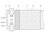
- FIG. 1 is a cross-sectional view schematically showing the inside of an example of a solid electrolytic capacitor according to the present disclosure
- FIG. FIG. 2 is a side cross-sectional view taken along line II-II of FIG. 1
- FIG. 3 is a plan view of the solid electrolytic capacitor before being sealed with an exterior resin
- a solid electrolytic capacitor according to the present disclosure includes a plurality of stacked capacitor elements, an anode lead terminal, and three or more junctions.
- Each of the plurality of capacitor elements has an anode portion and a cathode portion.
- An insulating portion may be provided between the anode portion and the cathode portion to electrically insulate them.
- the insulating portion may be made of, for example, insulating tape or insulating resin.
- the laminated anode part has a first surface arranged on one of the outermost sides in the stacking direction and a second surface arranged on the other outermost side in the stacking direction.
- the first surface may be the surface farther from the surface on which the solid electrolytic capacitor is mounted (the surface on which the exposed portions of the lead terminals are arranged, or the surface to be joined to a circuit board or the like).
- the second surface may be the surface closer to the mounting surface.
- the anode portion may be configured to include a portion of the anode body made of the valve metal of the capacitor element (a portion on one side with respect to the insulating portion).
- the cathode portion may be composed of a solid electrolyte layer and a cathode layer which are sequentially formed on the surface of the cathode forming portion, which is the remainder of the anode body (part on the other side with respect to the insulating portion).
- a dielectric layer is provided between the anode body and the solid electrolyte layer.
- the anode body may be a valve-acting metal foil, or may be a porous sintered body made of a valve-acting metal.
- the dielectric layer is formed at least on the surface of the cathode formation portion, which is the remainder of the anode body.
- the dielectric layer may be composed of an oxide (for example, aluminum oxide) formed on the surface of the anode body by a vapor phase method such as anodization or vapor deposition.
- the solid electrolyte layer is formed on the surface of the dielectric layer.
- the solid electrolyte layer may contain a conductive polymer.
- the solid electrolyte layer may further contain a dopant as needed.
- conductive polymer a known one used in solid electrolytic capacitors, such as a ⁇ -conjugated conductive polymer, can be used.
- conductive polymers include polymers having polypyrrole, polythiophene, polyaniline, polyfuran, polyacetylene, polyphenylene, polyphenylenevinylene, polyacene, and polythiophenevinylene as a basic skeleton.
- polymers having a basic skeleton of polypyrrole, polythiophene, or polyaniline are preferred.
- the above polymers also include homopolymers, copolymers of two or more monomers, and derivatives thereof (substituents having substituents, etc.).
- polythiophenes include poly(3,4-ethylenedioxythiophene) and the like. Conductive polymers may be used singly or in combination of two or more.
- the dopant for example, at least one selected from the group consisting of low-molecular-weight anions and polyanions is used.
- anions include sulfate ions, nitrate ions, phosphate ions, borate ions, organic sulfonate ions, and carboxylate ions, but are not particularly limited.
- Dopants that generate sulfonate ions include, for example, benzenesulfonic acid, p-toluenesulfonic acid, and naphthalenesulfonic acid.
- Polyanions include, for example, polymeric type polysulfonic acids and polymeric type polycarboxylic acids.
- Polymeric types of polysulfonic acids include polyvinylsulfonic acid, polystyrenesulfonic acid, polyallylsulfonic acid, polyacrylsulfonic acid, and polymethacrylsulfonic acid.
- Polymer-type polycarboxylic acids include polyacrylic acid and polymethacrylic acid.
- Polyanions also include polyestersulfonic acid, and phenolsulfonic acid novolak resins, and the like. However, polyanions are not limited to these.
- the solid electrolyte layer may further contain known additives and known conductive materials other than conductive polymers.
- a conductive material include at least one selected from the group consisting of conductive inorganic materials such as manganese dioxide and TCNQ complex salts.
- the cathode layer may be composed of a carbon layer formed on the surface of the solid electrolyte layer and a conductor layer formed on the surface of the carbon layer.
- the conductor layer may be composed of silver paste.
- the silver paste for example, a composition containing silver particles and a resin component (binder resin) can be used.
- a resin component a thermoplastic resin can be used, but it is preferable to use a thermosetting resin such as an imide resin or an epoxy resin.
- the anode lead terminal is electrically connected to at least one anode part.
- the anode lead terminal may be electrically connected to all the anode parts.
- the anode lead terminal may be made of copper or a copper alloy.
- the three or more joints join and electrically connect the laminated anode parts.
- the three or more joints include a first joint and a second joint.
- the first junction has a first area on the first surface of the laminated anode portion.
- the second junction has a second area that is less than the first area on the first surface of the stacked anode portion.
- the three or more joints include two or more types of joints having different areas on the first surface.
- the three or more joints may each extend from the first surface to the second surface. The existence of such three or more joint portions improves the joint quality between the laminated anode portions and reduces the variation in the electrical resistance value between the anode portions. As a result, variations in ESR of the solid electrolytic capacitor can be reduced.
- the three or more joints may be arranged linearly or non-linearly.
- the former it is conceivable to arrange three or more joints in a straight line along the width direction of the capacitor element.
- some (for example, two) joints are arranged linearly along the width direction of the capacitor element, and the remaining (for example, one) joints are arranged in the longitudinal direction of the capacitor element. It is conceivable to dispose away from the part of the joint in the. As another example of the latter, it is conceivable to arrange all junctions apart from each other in the longitudinal direction of the capacitor element.
- the area of the joint includes not only the portion of the joint made of the material of the anode portion but also the portion made of the melted material of the anode lead terminal. It refers to the area of the region including
- the first joint may be formed by welding from the first surface.
- the second joint may be formed by welding from the second surface.
- each joint has a larger area on the surface to which welding heat is input than on the opposite surface. That is, the first joint has a first area on the first surface and a third area on the second surface that is smaller than the first area.
- the second joint has a second area at the first surface and a fourth area at the second surface that is greater than the second area. The first area and the fourth area may be larger than the second area and the third area.
- Both the first joint and the second joint may be formed by welding from the first surface.
- both the first joint and the second joint may be formed by welding from the second surface.
- the first and second joints can be easily formed by welding from one direction.
- One of the first joint and the second joint is formed by welding from one of the first surface and the second surface, and the other of the first joint and the second joint is formed from the first surface and the second surface. It may be formed by welding from the other. In this case, it is easy to increase the volume of the entire joint portion while suppressing uneven distribution of the joint portion, so that the joint quality can be further improved.
- the first area may be twice or more the second area.
- the first area may be two times or more and eight times or less the second area.
- the ratio of the area of the joint with the largest area on the first surface to the area of the joint with the smallest area on the first surface may be 2 or more and 8 or less, or 4 or more and 8 or less. There may be.
- the fourth area may be twice or more the third area.
- the fourth area may be two times or more and eight times or less the third area.
- the ratio of the area of the joint with the largest area on the second surface to the area of the joint with the smallest area on the second surface may be 2 or more and 8 or less, or 4 or more and 8 or less. There may be.
- the pitch interval between the three or more joints may be 0.2 mm or more and 0.4 mm or less on the first surface or the second surface.
- three or more bonding portions are densely formed in the anode portion, so that the bonding quality between the stacked anode portions can be further improved.
- the pitch interval of the joints means the average value of the intervals between the centers of adjacent joints (for example, the center points when viewed from the normal direction of the first surface).
- the anode lead terminal may have a through hole at a position overlapping the second joint.
- the second joint can be easily formed by, for example, welding in which heat is input to the anode through the through hole.
- Various shapes such as a circle, an ellipse, a rectangle, and a polygon are conceivable as the shape of the through-hole.
- the size of the through-hole may be larger or smaller than the area (fourth area) of the second joint on the second surface. When the size of the through-hole is smaller than the area of the second joint on the second surface, a larger portion of the anode lead terminal can be melted into the second joint, thereby increasing the effect of reducing ESR. .
- a method for manufacturing a solid electrolytic capacitor according to the present disclosure includes a plurality of stacked capacitor elements each having an anode portion and a cathode portion, an anode lead terminal electrically connected to at least one anode portion, A method for manufacturing a solid electrolytic capacitor comprising: a lamination step, a temporary fixing step, and a bonding step.
- the laminated anode parts having the first surface and the second surface arranged on the outermost sides in one and the other of the stacking directions are crimped in the stacking direction with anode lead terminals to temporarily fix them.
- three or more joints are formed to join and electrically connect the plurality of temporarily fixed anode parts.
- the three or more joints include a first joint having a first area at the first surface and a second joint having a second area at the first surface that is less than the first area.
- the first joint is formed by welding from the first surface
- the second joint is formed by welding from the second surface.
- the presence of the three or more bonding portions improves the bonding quality between the stacked anode portions, Variation in electrical resistance between anode portions is reduced. As a result, variations in ESR of the solid electrolytic capacitor can be reduced.
- three or more joints may be formed by laser welding.
- three or more joining portions may be formed by welding other than laser welding (for example, resistance welding).
- the pitch interval between the three or more joints may be 0.2 mm or more and 0.4 mm or less on the first surface or the second surface.
- the anode lead terminal may have a through hole.
- the second joining portion may be formed by welding through the through hole. According to this configuration, welding heat can be directly input to the anode portion, so that the second joint portion can be easily formed.
- the solid electrolytic capacitor 10 includes a plurality of stacked capacitor elements 11, an anode lead terminal 17, a cathode lead terminal 18, three joints 20, and an exterior resin 23. Prepare.
- the plurality of capacitor elements 11 have anode portions 13 , cathode portions 14 and insulating portions 15 .
- Anode portion 13 is configured by a portion of anode body 12 made of a valve metal (for example, aluminum).
- Cathode portion 14 is composed of a solid electrolyte layer and a cathode layer which are sequentially formed on the surface of the anode forming portion, which is the remainder of anode body 12 .
- the insulating portion 15 is made of an insulating tape, and electrically insulates the anode portion 13 and the cathode portion 14 from each other.
- a dielectric layer is provided between the anode body 12 and the solid electrolyte layer.
- the stacked anode portions 13 are composed of a first surface 13a arranged on the outermost side in one of the stacking directions (vertical direction in FIG. 1) (upper side in FIG. 1) and an outermost surface 13a in the other side of the stacking direction (lower side in FIG. 1). and a second surface 13b disposed on the outside.
- the anode lead terminal 17 is electrically connected to the anode portion 13 of the capacitor element 11 .
- the anode lead terminal 17 is made of, for example, a copper alloy.
- the anode lead terminal 17 has a through hole 17a on the mounting surface (surface facing the second surface 13b) on which the anode portion 13 of the capacitor element 11 is mounted (see FIG. 2).
- the through hole 17a is a circular hole penetrating through the anode lead terminal 17 in the thickness direction.
- the through-hole 17a is arranged at a position overlapping with a second joint portion 22, which will be described later.
- the shape of the through-hole 17a is not limited to circular, and may be any other shape.
- the cathode lead terminal 18 is electrically connected to the cathode portion 14 of the capacitor element 11 .
- the cathode lead terminal 18 is made of, for example, a copper alloy.
- Cathode lead terminal 18 is bonded to cathode portion 14 of capacitor element 11 using conductive adhesive 16 . Adjacent cathode portions 14 are also joined together using conductive adhesive 16 .
- the three joints 20 join and electrically connect the laminated anode parts 13 .
- the three joints 20 include two first joints 21 and one second joint 22 .
- the second joint 22 is arranged between the two first joints 21 .
- the first joint portion 21 has a first area on the first surface 13 a of the laminated anode portion 13 .
- the second joint portion 22 has a second area smaller than the first area on the first surface 13a of the laminated anode portion 13 (see FIG. 3). In this embodiment, the first area is approximately three times the second area.
- the three joints 20 each extend from the first surface 13a to the second surface 13b.
- the first joint portion 21 is slightly tapered from the first surface 13a toward the second surface 13b.
- the second joint portion 22 is slightly tapered from the second surface 13b toward the first surface 13a.
- the first joint portion 21 and the second joint portion 22 need not be so tapered.
- the three joints 20 include two first joints 21 and one second joint 22, but may also include one first joint 21 and two second joints 22. .
- the first joint 21 may be arranged between two second joints 22 .
- two through-holes 17 a of anode lead terminal 17 may be arranged at positions overlapping first joint portion 21 .
- Four or more joints 20 may be provided.
- the first joint 21 is formed by welding (for example, laser welding) from the first surface 13a.
- the second joint portion 22 is formed by welding (for example, laser welding) from the second surface 13b through the through hole 17a.
- the pitch interval between the three joints 20 (the pitch interval in the horizontal direction in FIG. 2) is 0.2 mm or more and 0.4 mm or less on the first surface 13a or the second surface 13b. In this embodiment, the pitch interval is approximately 0.3 mm.
- the exterior resin 23 covers the plurality of capacitor elements 11 while partially exposing each of the anode lead terminal 17 and the cathode lead terminal 18 to the outside.
- the exterior resin 23 is made of an insulating resin material.
- the exposed portions of anode lead terminal 17 and cathode lead terminal 18 constitute external terminals of solid electrolytic capacitor 10 .
- a method for manufacturing the solid electrolytic capacitor 10 described above will be described.
- a method for manufacturing a solid electrolytic capacitor includes a preparation process, a lamination process, a curing process, a temporary fixing process, a bonding process, and a sealing process.
- a plurality of capacitor elements 11 each having an anode portion 13 and a cathode portion 14 are prepared.
- a plurality of capacitor elements 11 are laminated.
- a plurality of capacitor elements 11 may be stacked on anode lead terminal 17 and cathode lead terminal 18 .
- a plurality of capacitor elements 11 may be laminated with a conductive adhesive 16 interposed between the cathode portions 14 .
- the conductive adhesive 16 is cured. Curing of the conductive adhesive 16 may be performed, for example, by pressing an iron (not shown) as a heat source from above the plurality of laminated capacitor elements 11 .
- the laminated anode portion 13 having the first surface 13a and the second surface 13b is temporarily fixed by crimping the anode lead terminal 17 in the stacking direction.
- first joining portions 21 and one second joining portion 22 are formed to join and electrically connect the plurality of temporarily fixed anode portions 13 .
- first joint portion 21 is formed by laser welding from the first surface 13a
- second joint portion 22 is formed by laser welding from the second surface 13b.
- the second joining portion 22 is formed by laser welding through the through hole 17 a of the anode lead terminal 17 .
- the entirety is sealed with an exterior resin 23 so that a part of each of the anode lead terminal 17 and the cathode lead terminal 18 is exposed to the outside.
- the exposed portions of anode lead terminal 17 and cathode lead terminal 18 are bent along the outer surface of exterior resin 23 to form external terminals of solid electrolytic capacitor 10 .
- the solid electrolytic capacitor 10 of the present embodiment is obtained.
- ESR variation is the standard deviation of ESR in the ten solid electrolytic capacitors 10 .
- the ESR of the solid electrolytic capacitor 10 was measured as a resistance value at 100 kHz with an LCR meter.
- the "volume ratio of the joints" used in the description of each example and each comparative example below means the ratio of the total volume of all the joints 20 to the total volume of the laminated anode parts 13. For example, if the total volume of the stacked anode parts 13 is 100 and there are two junctions each having a volume of 10, the volume ratio of the junctions is 20%.
- the volume ratio of the joints was obtained by analyzing each joint 20 by X-ray CT. Specifically, an image is taken so that the cross-sectional area of all the joints in the side cross-sectional view as shown in FIG. 2 (here, the total of three) is maximized.
- the ratio of the cross-sectional area of all the joints to the sum of the cross-sectional areas of all the joints and the cross-sectional area of the anode portion is calculated as the "volume ratio of the joints.” It is desirable that the volume ratio of the joint is as large as possible.
- the volume ratio of the joint may be 50% or more, or 60% or more.
- the "area ratio of the joint" used in the description of each example and each comparative example below means the joint having the largest area on the first surface 13a with respect to the area of the joint 20 having the smallest area on the first surface 13a. 20 area ratio. For example, if the area of the former is 50 and the area of the latter is 100, the area ratio of the junction is two. The area ratio of the joints was obtained by observing each joint 20 with an optical microscope.
- the "pitch interval of joints" used in the description of each example and each comparative example below refers to the pitch interval of each joint 20 on the first surface 13a.
- the pitch interval of the joints was obtained by observing each joint 20 with an optical microscope.
- Example 1 a solid electrolytic capacitor 10 having the configuration of the above embodiment was produced. Next, a specific method thereof will be described.
- Anode body 12 was obtained by preparing an aluminum foil having a thickness of 100 ⁇ m and etching its surface. A dielectric layer containing aluminum oxide was formed on the surface of anode body 12 by immersing anode body 12 in an anodizing solution and applying a DC voltage. Next, the anode body 12 having the dielectric layer formed thereon and the counter electrode are immersed in a polymerization liquid containing polypyrrole as a conductive polymer, and electropolymerization is performed at a polymerization liquid temperature of 25° C. and a polymerization voltage of 3 V to form a dielectric layer.
- a solid electrolyte layer was formed on the surface of the The solid electrolyte layer was coated with a dispersion (carbon paste) of scaly graphite dispersed in water, and then heated at 200°C. Thus, a first layer comprising a solid electrolyte layer and a carbon layer was formed. A metal paste containing silver particles, a binder resin, and a solvent was applied to the surfaces of the carbon layers on both main surfaces of anode body 12 . After that, it was heated at 210° C. for 10 minutes to form a second layer, and a capacitor element 11 was obtained.
- the volume ratio of the joints is 54%
- the area ratio of the joints is 6.5
- the pitch interval of the joints is 0.35 mm.
- the ESR of the solid electrolytic capacitor 10 of Example 1 was 75.2 when the ESR of the solid electrolytic capacitor 10 of Comparative Example 2 was taken as 100.
- the ESR variation (standard deviation) in the solid electrolytic capacitor 10 of Example 1 was 15.2, with the ESR variation in the solid electrolytic capacitor 10 of Comparative Example 2 being 100.
- Example 2 the anode portion 13 of the temporarily fixed laminate was irradiated with three laser beams from the first surface 13a side. As a result, three first joints 21 were formed, and a laminate laser-welded at a total of three locations was obtained.
- the method of manufacturing the solid electrolytic capacitor 10 is the same as in Example 1 except for the above.
- the volume ratio of the joints is 54%, the area ratio of the joints is 1.5, and the pitch interval of the joints is 0.35 mm.
- the ESR of the solid electrolytic capacitor 10 of Example 2 was 75.2 when the ESR of the solid electrolytic capacitor 10 of Comparative Example 2 was taken as 100.
- the ESR variation (standard deviation) in the solid electrolytic capacitor 10 of Example 2 was 37.5, with the ESR variation in the solid electrolytic capacitor 10 of Comparative Example 2 being 100.
- Comparative Example 1 the anode portion 13 of the temporarily fixed laminate was irradiated with a laser at two points from the first surface 13a side. As a result, two first joints 21 were formed, and a laminate laser-welded at a total of two locations was obtained.
- the method of manufacturing the solid electrolytic capacitor 10 is the same as in Example 1 except for the above.
- the volume ratio of the joints is 37%, the area ratio of the joints is 1.0, and the pitch interval of the joints is 0.7 mm.
- the ESR of the solid electrolytic capacitor 10 of Comparative Example 1 was 75.2 when the ESR of the solid electrolytic capacitor 10 of Comparative Example 2 was taken as 100.
- the ESR variation (standard deviation) in the solid electrolytic capacitor 10 of Comparative Example 1 was 43.6 when the ESR variation in the solid electrolytic capacitor 10 of Comparative Example 2 was taken as 100.
- Comparative Example 2 the anode portion 13 of the temporarily fixed laminate was irradiated with a laser at one point from the first surface 13a side. As a result, one first joint portion 21 was formed, and a laminate laser-welded at one location was obtained.
- the method of manufacturing the solid electrolytic capacitor 10 is the same as in Example 1 except for the above.
- the solid electrolytic capacitor 10 of Comparative Example 2 has a joint portion volume ratio of 18%.
- the ESR of the solid electrolytic capacitor 10 of Comparative Example 2 was 100 as a reference value.
- the ESR variation (standard deviation) in the solid electrolytic capacitor 10 of Comparative Example 2 was 100 as a reference value.
- the present disclosure can be used for solid electrolytic capacitors and methods for manufacturing solid electrolytic capacitors.
Landscapes
- Engineering & Computer Science (AREA)
- Power Engineering (AREA)
- Microelectronics & Electronic Packaging (AREA)
- Manufacturing & Machinery (AREA)
- Fixed Capacitors And Capacitor Manufacturing Machines (AREA)
Priority Applications (3)
| Application Number | Priority Date | Filing Date | Title |
|---|---|---|---|
| US18/682,222 US12518932B2 (en) | 2021-08-23 | 2022-08-04 | Solid electrolytic capacitor capable of reducing ESR variation and method for manufacturing the same |
| CN202280057020.5A CN117836884A (zh) | 2021-08-23 | 2022-08-04 | 固体电解电容器和固体电解电容器的制造方法 |
| JP2023543784A JPWO2023026811A1 (https=) | 2021-08-23 | 2022-08-04 |
Applications Claiming Priority (2)
| Application Number | Priority Date | Filing Date | Title |
|---|---|---|---|
| JP2021-135805 | 2021-08-23 | ||
| JP2021135805 | 2021-08-23 |
Publications (1)
| Publication Number | Publication Date |
|---|---|
| WO2023026811A1 true WO2023026811A1 (ja) | 2023-03-02 |
Family
ID=85323153
Family Applications (1)
| Application Number | Title | Priority Date | Filing Date |
|---|---|---|---|
| PCT/JP2022/029896 Ceased WO2023026811A1 (ja) | 2021-08-23 | 2022-08-04 | 固体電解コンデンサおよび固体電解コンデンサの製造方法 |
Country Status (4)
| Country | Link |
|---|---|
| US (1) | US12518932B2 (https=) |
| JP (1) | JPWO2023026811A1 (https=) |
| CN (1) | CN117836884A (https=) |
| WO (1) | WO2023026811A1 (https=) |
Cited By (2)
| Publication number | Priority date | Publication date | Assignee | Title |
|---|---|---|---|---|
| WO2025052836A1 (ja) * | 2023-09-08 | 2025-03-13 | 株式会社村田製作所 | 固体電解コンデンサ、固体電解コンデンサの製造方法、および固体電解コンデンサの接続素子 |
| WO2025134990A1 (ja) * | 2023-12-18 | 2025-06-26 | パナソニックIpマネジメント株式会社 | 電解コンデンサおよび電解コンデンサの製造方法 |
Citations (5)
| Publication number | Priority date | Publication date | Assignee | Title |
|---|---|---|---|---|
| JPH0252325U (https=) * | 1988-10-04 | 1990-04-16 | ||
| JPH04243116A (ja) * | 1991-01-17 | 1992-08-31 | Matsushita Electric Ind Co Ltd | 固体電解コンデンサの製造方法 |
| JP2006140179A (ja) * | 2004-11-10 | 2006-06-01 | Tdk Corp | 固体電解コンデンサ及び固体電解コンデンサの製造方法 |
| JP2010153437A (ja) * | 2008-12-24 | 2010-07-08 | Sanyo Electric Co Ltd | 固体電解コンデンサ |
| JP2015136705A (ja) * | 2014-01-21 | 2015-07-30 | 株式会社神戸製鋼所 | 高強度鋼板のレーザ溶接継手およびその製造方法 |
Family Cites Families (3)
| Publication number | Priority date | Publication date | Assignee | Title |
|---|---|---|---|---|
| JPH05205984A (ja) * | 1992-01-27 | 1993-08-13 | Nec Corp | 積層型固体電解コンデンサ |
| JP5879491B2 (ja) * | 2012-02-28 | 2016-03-08 | パナソニックIpマネジメント株式会社 | 固体電解コンデンサ |
| JP7065301B2 (ja) * | 2016-12-28 | 2022-05-12 | パナソニックIpマネジメント株式会社 | 固体電解コンデンサおよびその製造方法 |
-
2022
- 2022-08-04 WO PCT/JP2022/029896 patent/WO2023026811A1/ja not_active Ceased
- 2022-08-04 CN CN202280057020.5A patent/CN117836884A/zh active Pending
- 2022-08-04 JP JP2023543784A patent/JPWO2023026811A1/ja active Pending
- 2022-08-04 US US18/682,222 patent/US12518932B2/en active Active
Patent Citations (5)
| Publication number | Priority date | Publication date | Assignee | Title |
|---|---|---|---|---|
| JPH0252325U (https=) * | 1988-10-04 | 1990-04-16 | ||
| JPH04243116A (ja) * | 1991-01-17 | 1992-08-31 | Matsushita Electric Ind Co Ltd | 固体電解コンデンサの製造方法 |
| JP2006140179A (ja) * | 2004-11-10 | 2006-06-01 | Tdk Corp | 固体電解コンデンサ及び固体電解コンデンサの製造方法 |
| JP2010153437A (ja) * | 2008-12-24 | 2010-07-08 | Sanyo Electric Co Ltd | 固体電解コンデンサ |
| JP2015136705A (ja) * | 2014-01-21 | 2015-07-30 | 株式会社神戸製鋼所 | 高強度鋼板のレーザ溶接継手およびその製造方法 |
Cited By (2)
| Publication number | Priority date | Publication date | Assignee | Title |
|---|---|---|---|---|
| WO2025052836A1 (ja) * | 2023-09-08 | 2025-03-13 | 株式会社村田製作所 | 固体電解コンデンサ、固体電解コンデンサの製造方法、および固体電解コンデンサの接続素子 |
| WO2025134990A1 (ja) * | 2023-12-18 | 2025-06-26 | パナソニックIpマネジメント株式会社 | 電解コンデンサおよび電解コンデンサの製造方法 |
Also Published As
| Publication number | Publication date |
|---|---|
| CN117836884A (zh) | 2024-04-05 |
| US20240347279A1 (en) | 2024-10-17 |
| JPWO2023026811A1 (https=) | 2023-03-02 |
| US12518932B2 (en) | 2026-01-06 |
Similar Documents
| Publication | Publication Date | Title |
|---|---|---|
| US9007743B2 (en) | Solid electrolytic capacitor | |
| US10629383B2 (en) | Solid electrolytic capacitor | |
| WO2022059459A1 (ja) | 固体電解コンデンサ | |
| US12518932B2 (en) | Solid electrolytic capacitor capable of reducing ESR variation and method for manufacturing the same | |
| US12255027B2 (en) | Electrolytic capacitor | |
| US10304635B2 (en) | Solid electrolytic capacitor having a directly bonded cathode layer | |
| JP2019145726A (ja) | 固体電解コンデンサ | |
| WO2022270195A1 (ja) | 固体電解コンデンサ | |
| US12494328B2 (en) | Solid electrolytic capacitor and manufacturing method therefor | |
| US12148576B2 (en) | Electrolytic capacitor | |
| CN103531361B (zh) | 固体电解电容器及其制造方法 | |
| JP2024142925A (ja) | 固体電解コンデンサ | |
| US12205773B2 (en) | Electrolytic capacitor and capacitor element | |
| JP2020072186A (ja) | 電解コンデンサ | |
| WO2023218931A1 (ja) | 固体電解コンデンサおよび固体電解コンデンサの製造方法 | |
| JP2008078312A (ja) | 固体電解コンデンサ | |
| JP7664526B2 (ja) | 固体電解コンデンサおよびその製造方法 | |
| US20240428998A1 (en) | Solid electrolytic capacitor | |
| JP7727956B2 (ja) | 固体電解コンデンサ | |
| US20240363291A1 (en) | Electrode foil for solid electrolytic capacitors, solid electrolytic capacitor element using same, and solid electrolytic capacitor | |
| US20240412927A1 (en) | Solid electrolytic capacitor | |
| US20250191852A1 (en) | Solid electrolytic capacitor and production method for solid electrolytic capacitor | |
| WO2024004989A1 (ja) | 固体電解コンデンサ素子および固体電解コンデンサ | |
| JP6913875B2 (ja) | 電解コンデンサ | |
| WO2025169887A1 (ja) | 固体電解コンデンサ |
Legal Events
| Date | Code | Title | Description |
|---|---|---|---|
| 121 | Ep: the epo has been informed by wipo that ep was designated in this application |
Ref document number: 22861102 Country of ref document: EP Kind code of ref document: A1 |
|
| WWE | Wipo information: entry into national phase |
Ref document number: 2023543784 Country of ref document: JP |
|
| WWE | Wipo information: entry into national phase |
Ref document number: 202280057020.5 Country of ref document: CN |
|
| NENP | Non-entry into the national phase |
Ref country code: DE |
|
| 122 | Ep: pct application non-entry in european phase |
Ref document number: 22861102 Country of ref document: EP Kind code of ref document: A1 |
|
| WWG | Wipo information: grant in national office |
Ref document number: 18682222 Country of ref document: US |