WO2023024111A1 - Inverting conversion circuit and photovoltaic power generation system - Google Patents
Inverting conversion circuit and photovoltaic power generation system Download PDFInfo
- Publication number
- WO2023024111A1 WO2023024111A1 PCT/CN2021/115149 CN2021115149W WO2023024111A1 WO 2023024111 A1 WO2023024111 A1 WO 2023024111A1 CN 2021115149 W CN2021115149 W CN 2021115149W WO 2023024111 A1 WO2023024111 A1 WO 2023024111A1
- Authority
- WO
- WIPO (PCT)
- Prior art keywords
- unit
- capacitor
- voltage
- switch
- switch module
- Prior art date
Links
- 238000006243 chemical reaction Methods 0.000 title claims abstract description 126
- 238000010248 power generation Methods 0.000 title claims abstract description 20
- 239000003990 capacitor Substances 0.000 claims abstract description 159
- 238000004146 energy storage Methods 0.000 claims abstract description 52
- 230000009466 transformation Effects 0.000 claims description 5
- 238000010586 diagram Methods 0.000 description 41
- 238000000034 method Methods 0.000 description 12
- 239000004065 semiconductor Substances 0.000 description 11
- 238000012545 processing Methods 0.000 description 9
- 238000004590 computer program Methods 0.000 description 7
- 230000006870 function Effects 0.000 description 7
- 230000005669 field effect Effects 0.000 description 4
- 238000004519 manufacturing process Methods 0.000 description 3
- 238000012986 modification Methods 0.000 description 3
- 230000004048 modification Effects 0.000 description 3
- 238000012546 transfer Methods 0.000 description 3
- 230000005540 biological transmission Effects 0.000 description 2
- 230000008859 change Effects 0.000 description 2
- 238000013461 design Methods 0.000 description 2
- 230000001939 inductive effect Effects 0.000 description 2
- 229910044991 metal oxide Inorganic materials 0.000 description 2
- 150000004706 metal oxides Chemical class 0.000 description 2
- 230000008569 process Effects 0.000 description 2
- HEZMWWAKWCSUCB-PHDIDXHHSA-N (3R,4R)-3,4-dihydroxycyclohexa-1,5-diene-1-carboxylic acid Chemical compound O[C@@H]1C=CC(C(O)=O)=C[C@H]1O HEZMWWAKWCSUCB-PHDIDXHHSA-N 0.000 description 1
- JMASRVWKEDWRBT-UHFFFAOYSA-N Gallium nitride Chemical compound [Ga]#N JMASRVWKEDWRBT-UHFFFAOYSA-N 0.000 description 1
- 125000004122 cyclic group Chemical group 0.000 description 1
- 238000005516 engineering process Methods 0.000 description 1
- 230000003287 optical effect Effects 0.000 description 1
- HBMJWWWQQXIZIP-UHFFFAOYSA-N silicon carbide Chemical compound [Si+]#[C-] HBMJWWWQQXIZIP-UHFFFAOYSA-N 0.000 description 1
- 239000007787 solid Substances 0.000 description 1
Images


Classifications
-
- H—ELECTRICITY
- H02—GENERATION; CONVERSION OR DISTRIBUTION OF ELECTRIC POWER
- H02M—APPARATUS FOR CONVERSION BETWEEN AC AND AC, BETWEEN AC AND DC, OR BETWEEN DC AND DC, AND FOR USE WITH MAINS OR SIMILAR POWER SUPPLY SYSTEMS; CONVERSION OF DC OR AC INPUT POWER INTO SURGE OUTPUT POWER; CONTROL OR REGULATION THEREOF
- H02M1/00—Details of apparatus for conversion
- H02M1/0048—Circuits or arrangements for reducing losses
- H02M1/0054—Transistor switching losses
- H02M1/0058—Transistor switching losses by employing soft switching techniques, i.e. commutation of transistors when applied voltage is zero or when current flow is zero
-
- H—ELECTRICITY
- H02—GENERATION; CONVERSION OR DISTRIBUTION OF ELECTRIC POWER
- H02M—APPARATUS FOR CONVERSION BETWEEN AC AND AC, BETWEEN AC AND DC, OR BETWEEN DC AND DC, AND FOR USE WITH MAINS OR SIMILAR POWER SUPPLY SYSTEMS; CONVERSION OF DC OR AC INPUT POWER INTO SURGE OUTPUT POWER; CONTROL OR REGULATION THEREOF
- H02M3/00—Conversion of dc power input into dc power output
- H02M3/02—Conversion of dc power input into dc power output without intermediate conversion into ac
- H02M3/04—Conversion of dc power input into dc power output without intermediate conversion into ac by static converters
- H02M3/10—Conversion of dc power input into dc power output without intermediate conversion into ac by static converters using discharge tubes with control electrode or semiconductor devices with control electrode
- H02M3/145—Conversion of dc power input into dc power output without intermediate conversion into ac by static converters using discharge tubes with control electrode or semiconductor devices with control electrode using devices of a triode or transistor type requiring continuous application of a control signal
- H02M3/155—Conversion of dc power input into dc power output without intermediate conversion into ac by static converters using discharge tubes with control electrode or semiconductor devices with control electrode using devices of a triode or transistor type requiring continuous application of a control signal using semiconductor devices only
- H02M3/156—Conversion of dc power input into dc power output without intermediate conversion into ac by static converters using discharge tubes with control electrode or semiconductor devices with control electrode using devices of a triode or transistor type requiring continuous application of a control signal using semiconductor devices only with automatic control of output voltage or current, e.g. switching regulators
-
- H—ELECTRICITY
- H02—GENERATION; CONVERSION OR DISTRIBUTION OF ELECTRIC POWER
- H02J—CIRCUIT ARRANGEMENTS OR SYSTEMS FOR SUPPLYING OR DISTRIBUTING ELECTRIC POWER; SYSTEMS FOR STORING ELECTRIC ENERGY
- H02J3/00—Circuit arrangements for ac mains or ac distribution networks
- H02J3/38—Arrangements for parallely feeding a single network by two or more generators, converters or transformers
- H02J3/381—Dispersed generators
-
- H—ELECTRICITY
- H02—GENERATION; CONVERSION OR DISTRIBUTION OF ELECTRIC POWER
- H02M—APPARATUS FOR CONVERSION BETWEEN AC AND AC, BETWEEN AC AND DC, OR BETWEEN DC AND DC, AND FOR USE WITH MAINS OR SIMILAR POWER SUPPLY SYSTEMS; CONVERSION OF DC OR AC INPUT POWER INTO SURGE OUTPUT POWER; CONTROL OR REGULATION THEREOF
- H02M3/00—Conversion of dc power input into dc power output
- H02M3/01—Resonant DC/DC converters
-
- H—ELECTRICITY
- H02—GENERATION; CONVERSION OR DISTRIBUTION OF ELECTRIC POWER
- H02M—APPARATUS FOR CONVERSION BETWEEN AC AND AC, BETWEEN AC AND DC, OR BETWEEN DC AND DC, AND FOR USE WITH MAINS OR SIMILAR POWER SUPPLY SYSTEMS; CONVERSION OF DC OR AC INPUT POWER INTO SURGE OUTPUT POWER; CONTROL OR REGULATION THEREOF
- H02M7/00—Conversion of ac power input into dc power output; Conversion of dc power input into ac power output
- H02M7/42—Conversion of dc power input into ac power output without possibility of reversal
- H02M7/44—Conversion of dc power input into ac power output without possibility of reversal by static converters
- H02M7/48—Conversion of dc power input into ac power output without possibility of reversal by static converters using discharge tubes with control electrode or semiconductor devices with control electrode
- H02M7/53—Conversion of dc power input into ac power output without possibility of reversal by static converters using discharge tubes with control electrode or semiconductor devices with control electrode using devices of a triode or transistor type requiring continuous application of a control signal
- H02M7/537—Conversion of dc power input into ac power output without possibility of reversal by static converters using discharge tubes with control electrode or semiconductor devices with control electrode using devices of a triode or transistor type requiring continuous application of a control signal using semiconductor devices only, e.g. single switched pulse inverters
- H02M7/5387—Conversion of dc power input into ac power output without possibility of reversal by static converters using discharge tubes with control electrode or semiconductor devices with control electrode using devices of a triode or transistor type requiring continuous application of a control signal using semiconductor devices only, e.g. single switched pulse inverters in a bridge configuration
- H02M7/53871—Conversion of dc power input into ac power output without possibility of reversal by static converters using discharge tubes with control electrode or semiconductor devices with control electrode using devices of a triode or transistor type requiring continuous application of a control signal using semiconductor devices only, e.g. single switched pulse inverters in a bridge configuration with automatic control of output voltage or current
-
- H—ELECTRICITY
- H02—GENERATION; CONVERSION OR DISTRIBUTION OF ELECTRIC POWER
- H02J—CIRCUIT ARRANGEMENTS OR SYSTEMS FOR SUPPLYING OR DISTRIBUTING ELECTRIC POWER; SYSTEMS FOR STORING ELECTRIC ENERGY
- H02J2300/00—Systems for supplying or distributing electric power characterised by decentralized, dispersed, or local generation
- H02J2300/20—The dispersed energy generation being of renewable origin
- H02J2300/22—The renewable source being solar energy
- H02J2300/24—The renewable source being solar energy of photovoltaic origin
-
- Y—GENERAL TAGGING OF NEW TECHNOLOGICAL DEVELOPMENTS; GENERAL TAGGING OF CROSS-SECTIONAL TECHNOLOGIES SPANNING OVER SEVERAL SECTIONS OF THE IPC; TECHNICAL SUBJECTS COVERED BY FORMER USPC CROSS-REFERENCE ART COLLECTIONS [XRACs] AND DIGESTS
- Y02—TECHNOLOGIES OR APPLICATIONS FOR MITIGATION OR ADAPTATION AGAINST CLIMATE CHANGE
- Y02E—REDUCTION OF GREENHOUSE GAS [GHG] EMISSIONS, RELATED TO ENERGY GENERATION, TRANSMISSION OR DISTRIBUTION
- Y02E10/00—Energy generation through renewable energy sources
- Y02E10/50—Photovoltaic [PV] energy
- Y02E10/56—Power conversion systems, e.g. maximum power point trackers
Definitions
- This application relates to the field of electronic power, in particular to an inverting conversion circuit and a photovoltaic power generation system.
- the DC combiner box mainly needs to consider the current carrying capacity of the downstream cables and the cable loss caused by excessive current. Therefore, the DC combiner box needs to reduce the output current under the premise of ensuring the output power.
- the DC combiner box includes a direct current-to-direct current converter (DC-DC) circuit and a resonant switched capacitor converter (RSCC) part.
- DC-DC direct current-to-direct current converter
- RSCC resonant switched capacitor converter
- the four photovoltaic modules in the upper half of Figure 1 are respectively connected with the corresponding DC-DC in the DC combiner box, and the DC-DC circuit outputs V BUS+ in parallel, and inputs V BUS+ to the DC bus; the four photovoltaic modules in the lower half of Figure 1 A photovoltaic module is also connected to the DC-DC circuit, the DC-DC circuit is output in parallel, and connected to the resonant switched capacitor converter (RSCC), the RSCC circuit outputs V BUS- in parallel, and outputs V BUS- to the DC bus
- RSCC resonant switched capacitor converter
- V BUS+ and V BUS- are connected in series, so that the total voltage output to the rear inverter is twice the V BUS voltage, and finally through the grid-connected cabinet and the transformer to the more critical AC load (such as the power grid) power supply.
- the DC combiner box can increase the voltage on the DC bus under the premise of outputting the same power, thereby reducing the output current.
- FIG. 2 is a schematic diagram of the topological structure of the current DC-DC and RSCC circuits.
- the DC-DC circuit is used to connect with the photovoltaic module, receive the DC voltage Vin input by the photovoltaic module, and boost the DC voltage Vin input by the photovoltaic module to obtain V BUS+ , and V BUS+ falls to the series connected C1 and On C2, and the RSCC circuit part is used to connect with the DC-DC circuit, use the V BUS+ output by the DC-DC circuit to reverse the V BUS+ , so as to obtain V BUS- , V BUS- falls on the capacitor C3, the circuit’s
- the total output voltage is twice V BUS .
- the present application provides a flip conversion circuit and a photovoltaic power generation system, which can significantly reduce the number of semiconductor devices compared with the existing DC-DC plus RSCC circuit topology, reduce power supply costs, reduce losses and improve conversion efficiency .
- the present application provides an inversion conversion circuit
- the inversion conversion circuit includes: a first access terminal S1, a second access terminal S2, a third access terminal S3, a half-bridge switch unit, an output capacitor unit, a resonant unit, a series diode unit, an energy storage switch unit, an input unit, an output unit and a controller
- the half-bridge switch unit includes N switching devices, where N is an even number
- the half-bridge switch unit is connected between S1 and S2, and the series diode unit is connected
- the output capacitor unit is connected in parallel at both ends of the series diode unit, the input unit is connected between S1 and S2, and the output unit is connected between S1 and S3
- the energy storage switch unit includes at least one switching device and a first Diode D1, at least one switching device is connected in series with the first diode D1
- the resonance unit includes a first capacitor and a first inductor, the first end of the first inductor is connected to the half-bridge switch unit, and the
- the cost of components in the circuit, the board space occupied by the entire circuit and the device loss can be significantly reduced.
- the structure provided by the present application can also significantly reduce The number of diodes is reduced, so that the switching device in the flip-flop conversion circuit has the condition of zero voltage conduction, and the switching loss is reduced.
- the specific quantity of the switching devices in the above-mentioned half-bridge switching unit and the energy storage switching unit may be related to the magnitude of the first voltage and the withstand voltage capability of the switching devices.
- the specific design of the switching devices in the half-bridge switching unit and the energy storage switching unit When the quantity is large, if the first voltage is large and the withstand voltage capability of the switch device is low, multiple switch devices can be connected in series to divide the first voltage, so as to ensure that the switch device with low withstand voltage can work normally.
- the half-bridge switch unit includes: a first switch module and a second switch module; the first switch module and the second switch module respectively contain a switch device; optionally, the first switch module The first electrode of the switching device is connected to S1, the second electrode of the switching device in the first switching module is connected to the first electrode of the switching device in the second switching module, and the second electrode of the switching device in the second switching module connected to S2; one end of the first inductor is connected to the second electrode of the switch device in the first switch module.
- the half-bridge switch unit includes: a first switch module and a second switch module; the first switch module and the second switch module respectively include a plurality of switch devices; , each adjacent two switching devices are connected to each other in series and/or in parallel.
- the series diode unit specifically includes: a second diode D2 and a third diode D3; the cathode of D2 is connected to S2, the anode of D2 is connected to the cathode of D3, and the anode of D3 is connected to S3 Connection; the second end of the first inductor in the resonant unit is connected between D2 and D3.
- the series diode unit in the embodiment of the present application may also be called a clamp unit, and the clamp unit may be used to limit the voltage of the second access terminal S2 from changing.
- the controller can set the ratio of the first voltage to the second voltage according to different scenarios, and the inversion conversion circuit provided by the embodiment of the present application can be applied in scenarios such as boost conversion, buck conversion, and polarity conversion.
- boost conversion scenario the second voltage may be greater than the first voltage.
- buck conversion scenario the second voltage may be smaller than the first voltage.
- polarity change the second voltage may be an opposite number to the first voltage.
- the range of the second voltage may be determined according to the range of the first voltage provided by the input unit.
- the controller is specifically configured to: when the ratio of the first voltage to the second voltage is set as the first target ratio, control the switching device in the second switching module to turn on, The first capacitance and the first inductance in the resonance unit are formed to resonate, and the resonance unit reversely charges the output capacitance in the output capacitance unit through D3 in the series diode unit; the resonance current on the first inductance in the resonance unit is detected When it is 0, control the switch device in the second switch module to turn off; control the switch device in the first switch module to conduct and the switch device in the energy storage switch unit to conduct; the first voltage charges the first inductor; The switch device in the switch module is turned on, so that the first capacitor and the first inductor in the resonance unit form resonance; when it is detected that the resonance current on the first inductor in the resonance unit is 0, control the switch in the first switch module The device is disconnected.
- the controller controls the switching device in the second switching module to turn on, so that the first capacitor in the resonance unit And the first inductance forms a resonance; when it is detected that the resonance current on the first inductance in the resonance unit is 0, the switching device in the second switching module is controlled to be turned off; the switching device in the first switching module is controlled to be turned on, so that The first capacitor and the first inductor in the resonance unit form a resonance; when it is detected that the resonance current on the first inductor in the resonance unit is 0, the switching device in the first switch module is controlled to be turned off.
- the flip conversion circuit also includes: a second capacitor and a third capacitor, one end of the second capacitor It is connected with S1, the other end is connected with one end of the third capacitor, and the other end of the third capacitor is connected with S2.
- the first switch module includes: a first switch tube Q1, a second switch tube Q2, and a fourth diode D4;
- the second switch module includes: a third switch tube Q3, a fourth switch tube Q4 And the fifth diode D5;
- the first electrode of Q1 is connected to S1, the second electrode of Q1 is connected to the first electrode of Q2, the second electrode of Q1 is connected to the first end of the first capacitor, and the negative electrode of D4 is connected to Q1
- the second electrode of Q3 is connected to the first terminal of the first capacitor, the second electrode of Q3 is connected to the first electrode of Q4, the second electrode of Q4 is connected to S2, the positive pole of D5 is connected to the first electrode of Q3 The two electrodes are connected; the positive pole of D4 is connected with the negative pole of D5.
- the flip conversion circuit further includes: a fourth capacitor and a fifth capacitor, one end of the fourth capacitor is connected to S1, the other end is connected to one end of the fifth capacitor, and the other end of the fifth capacitor is connected to S2 , the other end of the fourth capacitor is also connected to the positive pole of D4.
- the controller is further configured to: when the ratio of the first voltage to the second voltage is set as the first target ratio, control Q3 and Q4 in the second switch module to conduct, so that the resonance unit The first capacitance and the first inductance in the resonance unit form a resonance, and the resonance unit reversely charges the output capacitance in the output capacitance unit through D3 in the series diode unit; when it is detected that the resonance current on the first inductance in the resonance unit is 0 , control Q3 and Q4 in the second switch module to turn off; control Q1 and Q2 in the first switch module to turn on and switch devices in the energy storage switch unit to turn on; the first voltage charges the first inductor; control the first switch Q1 and Q2 in the module are turned on, so that the first capacitor and the first inductance in the resonance unit form resonance; when it is detected that the resonance current on the first inductance in the resonance unit is 0, control Q1 in the first switch module And Q2 is turned off; Q3 in the first switch module is controlled
- the controller is further configured to: when the ratio of the first voltage to the second voltage is set as the second target ratio, control Q3 in the second switch module to conduct, and the first voltage in the resonance unit
- the inductance current on an inductor reversely charges the output capacitor in the output capacitor unit through Q3, D5, and D3; controls the conduction of Q3 and Q4 in the first switch module, so that the first capacitor and the first inductance in the resonance unit form Resonance; when it is detected that the resonance current on the first inductor in the resonance unit is 0, control Q3 and Q4 in the second switch module to be disconnected; control Q2 in the second switch module to conduct, and the first in the resonance unit
- the inductor current on the inductor reversely charges the output capacitor in the output capacitor unit through Q2, D4, and D3; controls the conduction of Q1 and Q2 in the first switch module, so that the first capacitor and the first inductor in the resonance unit form resonance ; When it is detected that the resonant current on the first inductor in the
- the controller is further configured to: when the ratio of the first voltage to the second voltage is set as the third target ratio, control the conduction of Q3 in the second switch module; control the Q3 in the resonance unit When the resonant current on the first inductor is 0, control Q3 in the second switch module to turn off; control Q1 and Q2 in the first switch module to turn on and switch devices in the energy storage switch unit to turn on; the first voltage is given to the second Inductive charging; control Q1 and Q2 in the first switch module to be turned on and switch devices in the energy storage switch unit to be turned off; make the first capacitor and the first inductance in the resonant unit form resonance; control Q3 in the second switch module conduction.
- the energy storage switch unit includes: a sixth capacitor connected in parallel with the first diode D1, and the sixth capacitor is used to eliminate a voltage spike of at least one switching device in the energy storage switch unit.
- the input unit specifically includes: an input DC source and a DC boost circuit; the DC boost circuit is configured to boost the first voltage of the input DC source.
- the present application provides a photovoltaic power generation system, including the inversion conversion circuit provided in the first aspect, a plurality of photovoltaic strings, and an inverter circuit; a plurality of photovoltaic strings are connected to the input unit in the inversion conversion circuit; The output unit of the circuit is connected to the inverter circuit; the flip conversion circuit is used to convert the first voltage output by multiple photovoltaic strings into a second voltage, and output the second voltage at the output unit; the output terminal of the inverter circuit is connected to the grid , so as to convert the second voltage into AC voltage and supply it to the power grid.
- FIG. 1 is a structural schematic diagram of an existing photovoltaic power generation system
- Figure 2 is a schematic diagram of the current DC-DC and RSCC circuit topology
- Fig. 3 is a structural schematic diagram of an inversion conversion circuit
- FIG. 4 is a schematic structural diagram of a half-bridge switch unit
- FIG. 5 is a schematic structural diagram of a half-bridge switch unit
- Fig. 6 is the structural representation of series diode unit
- Fig. 7A-Fig. 7C are the on-off schematic diagrams of the inversion conversion circuit 1;
- FIG. 7D is a timing diagram 1 of an inversion conversion circuit
- FIG. 8C is a timing diagram 2 of the inversion conversion circuit
- FIG. 9 is a schematic diagram of structure 1 corresponding to an inversion conversion circuit
- FIG. 10 is a schematic diagram of structure 2 corresponding to the inversion conversion circuit
- FIG. 11 is a schematic diagram of structure three corresponding to the inversion conversion circuit
- FIG. 12A is a schematic diagram of structure four corresponding to an inversion conversion circuit
- FIG. 12B is a schematic diagram of structure five corresponding to the inversion conversion circuit
- FIG. 13A is a schematic diagram of the structure six corresponding to the inversion conversion circuit
- FIG. 13B is a schematic diagram of structure 7 corresponding to the inversion conversion circuit
- FIG. 14A is a schematic diagram of a structure eight corresponding to an inversion conversion circuit
- FIG. 14B is a schematic diagram of structure nine corresponding to the inversion conversion circuit
- FIG. 15A is a schematic diagram of a corresponding structure 10 of an inversion conversion circuit
- FIG. 15B is a schematic diagram of structure eleven corresponding to the inversion conversion circuit
- FIG. 16A is a schematic diagram of structure twelve corresponding to the inversion conversion circuit
- FIG. 16B is a schematic diagram of structure 13 corresponding to the inversion conversion circuit
- Figure 17A- Figure 17D is the third on-off schematic diagram of the inversion conversion circuit
- FIG. 17E is a timing diagram three of the inversion conversion circuit
- 18A-18D are on-off schematic diagrams 4 of the flip conversion circuit
- FIG. 18E is a timing diagram four of the inversion conversion circuit
- Fig. 19A-Fig. 19D are on-off schematic diagrams five of the inversion conversion circuit
- FIG. 19E is a timing diagram five of the inversion conversion circuit
- Fig. 20 is a schematic structural diagram of a photovoltaic power generation system.
- FIG. 1 shows a typical photovoltaic power generation system.
- the DC combiner box In a photovoltaic power generation system, the DC combiner box must consider the current carrying capacity of the downstream cables and the cable loss. Therefore, the DC combiner box can reduce the cable loss only by reducing the output current under the premise of ensuring the output power.
- the current DC combiner box mainly includes DC-DC and RSCC circuits.
- the four photovoltaic modules in the upper half of Figure 1 are respectively connected to the DC-DC circuit in the DC combiner box, and the DCDC circuit outputs V BUS+ in parallel, and V BUS+ is input to the DC bus;
- the four photovoltaic modules in the lower half of Figure 1 are also connected to the DC-DC circuit and output in parallel, and then connected to the resonant switched capacitor circuit RSCC circuit, the RSCC circuit outputs V BUS- , and V BUS- is output to
- the DC combiner box can increase the voltage on the DC bus under the premise of outputting the same power, thereby reducing the output current.
- the present application provides a flip conversion circuit, which can significantly reduce the number of semiconductor devices in the DC combiner box compared to the topology composed of the DC-DC circuit and the RSCC circuit in the prior art, on the premise of reducing the cost , which improves the conversion efficiency.
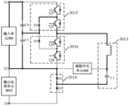
- the inversion conversion circuit 300 may include: a first access terminal S1, a second access terminal S2, a third access terminal S3, a half-bridge switch unit 3011, and an output capacitor unit 3012 , a resonant unit 3013, a series diode unit 3014, an energy storage switch unit 302, an input unit 303, an output unit 304, and a controller 305, wherein the half-bridge switch unit 3011 includes N switching devices, and N is an even number;
- controller 305 can be connected with the half-bridge switch unit 3011 and the energy storage switch unit 302 , so as to control the switching devices in the switch unit 3011 and the energy storage switch unit 302 .
- the input positive terminal 303a of the input unit 303 is connected to the first access terminal S1
- the input negative terminal 303b of the output unit 303 is connected to the second input terminal S2.
- the first terminal 3012a of the output capacitor unit 3012 is connected to the first terminal S2, and the second terminal 3012b of the output capacitor unit 3012 is connected to the third access terminal S3; the first terminal 3011a of the half-bridge switch unit 3011 is connected to the first terminal S3.
- the second terminal 3011b of the half-bridge switch unit 3011 is connected to the second access terminal S2, the third terminal 3011c of the half-bridge switch unit 3011 is connected to the controller 305, and the fourth terminal 3011d of the half-bridge switch unit 3011 is connected to the resonance
- the first terminal 3013a of the unit 3013 is connected; the first terminal 3014a of the series diode unit 3014 is connected to the second access terminal S2, the second terminal 3014b of the series diode unit 3014 is connected to the third access terminal S3, and the series diode unit 3014
- the third end 3014c is connected to the second end 3013b of the resonance unit 3013 .
- the first end 302a of the energy storage switch unit 302 is connected between the second end 3011b of the half-bridge switch unit 3011 and the first end 3014a of the series diode unit 3014, and the second end 302b of the energy storage switch unit 302 is connected to the resonance unit
- the third terminal 3013c of the energy storage switch unit 302 is connected to the controller 305 .
- the positive output terminal 303a of the output unit 304 is connected to the first access terminal S1, and the negative output terminal 303b of the output unit 304 is connected to the third access terminal S3.
- the input unit 303 in the embodiment of the present application may further include at least one capacitor to stabilize the first voltage and store electric energy.
- the resonant inductor and resonant capacitor in the resonant unit 3013 in the embodiment of the present application may be connected in series.
- the resonant unit 3013 may include a first capacitor and a first inductor connected in series, a first end of the first inductor is connected to the half-bridge switch unit 3011, a second end of the first capacitor is connected to the series diode unit 3014 connected; the second end of the first inductor is connected to the first end of the first capacitor.
- the first inductor and the first capacitor in the resonant unit 3013 provided in the embodiment of the present application are used to transfer energy, and enable the switching devices in the half-bridge switching unit 3011 and the energy storage switching unit 302 to work in a soft switching state.
- the resonant unit 3013 can be used as an energy transfer unit (energy relay component or energy relay module), in other words, the resonant unit 3013 can be used as an energy transfer medium, first accepting the charging of the first voltage of the input unit 303, after being charged Provide electrical energy to the output capacitor unit 3012, charge the output capacitor unit 3012, and finally the output unit 304 receives the electrical energy jointly output by the input unit 303 and the output capacitor unit 3012, so as to convert the input first voltage into a higher voltage for output .
- energy transfer unit energy relay component or energy relay module
- the half-bridge switching unit 3011 and the switching devices in the energy storage switching unit 302 in the embodiment of the present application may be metal oxide semiconductor field effect transistors (metal oxide semiconductor field effect transistors, MOSFETs), bipolar junction transistors (bipolar junction transistors) , BJT), insulated gate bipolar transistor (insulated gate bipolar transistor, IGBT), field effect transistor (field effect transistor, FET), silicon carbide (SiC) or gallium nitride (GaN) power tube and other types of switches
- MOSFETs metal oxide semiconductor field effect transistors
- BJT bipolar junction transistors
- IGBT insulated gate bipolar transistor
- field effect transistor field effect transistor
- FET field effect transistor
- SiC silicon carbide
- GaN gallium nitride
- the control electrode of the switch is the gate
- the first electrode of the switch can be the source of the switching device
- the second electrode can be the drain of the switching device
- the first electrode can be the drain of the switch
- the second electrode can be the drain of the switch.
- the two electrodes can be the source of the switch.
- both the first end of the main power tube and the first end of the auxiliary power tube can be a source (source) pole, and can also be a drain (drain) pole.
- the number of switching devices in the half-bridge switching unit 3011 and the energy storage switching unit 302 may be related to the magnitude of the first voltage and the withstand voltage capability of the switching devices. In the specific design of the half-bridge switching unit 3011 and the energy storage switching unit 302 When the number of switching devices is large, when the first voltage is large and the withstand voltage capability of the switch device is low, multiple switch devices can be connected in series to divide the first voltage, thereby ensuring a switch with low withstand voltage The device can work normally.
- the output capacitor unit 3012 provided in the embodiment of the present application is connected in parallel at both ends of the series diode unit 3014 .
- the series diode unit 3014 includes a plurality of series diodes, the anode of each diode in the series series diodes is connected to the cathode of the adjacent diode, the first diode is connected to S2, and the last diode is connected to S3.
- the output capacitor unit 3012 may include at least one capacitor. It should be understood that the series diode unit 3014 may also be composed of other elements, so as to realize the role or function of the series diode unit 3014 in the embodiment of the present application. The embodiment of the present invention does not make too many limitations on this.
- the controller 305 provided in the embodiment of the present application is used to control the switching off of the switching devices in the half-bridge switching unit 3011 and the energy storage switching unit 302, and transform the first voltage input by the input unit 303 into the second voltage, and output the second voltage at the output unit 304 .
- the controller 305 in the application embodiment may be a general-purpose central processing unit (central processing unit, CPU), a general-purpose processor, digital signal processing (digital signal processing, DSP), application specific integrated circuits (application specific integrated circuits, ASIC), field programmable gate array (field programmable gate array, FPGA) or other programmable logic devices, transistor logic devices, hardware components or any combination thereof. It can implement or execute the various illustrative logical blocks, modules and circuits described in connection with the present disclosure.
- the above-mentioned processor may also be a combination to realize computing functions, for example, a combination of one or more microprocessors, a combination of DSP and a microprocessor, and so on.
- the controller 305 controls the half-bridge switch unit 3011 to transmit the first voltage provided by the input unit 303 to the output filter unit 3014, it controls the half-bridge switch unit 3011 to transmit the first voltage provided by the input unit 303
- the electric energy is transmitted to the resonance unit 3013 , so that the input unit 303 can charge the resonance unit 3013 .
- the resonant unit 3013 charges the output capacitor unit 3012 , and the output unit 304 outputs the second voltage.
- the controller 305 provided in the embodiment of the present application can control the half-bridge switch unit 3011 to transmit the electric energy provided by the input unit 303 to the output capacitor unit 3012, so as to realize the charging of the output capacitor unit 3012 by the input unit 303 .
- the controller 305 can also send a control signal or a driving signal to the half-bridge switch unit 301 . After the half-bridge switch unit 301 receives the control signal or the driving signal, it transmits the electric energy provided by the input unit 303 to the output capacitor unit 3012 .
- the half-bridge switch unit 301 may also not transmit the electric energy provided by the input unit 303 to the output capacitor unit 3012 after not receiving the control signal or the driving signal.
- the controller 305 can also control the half-bridge switch unit 3011 to transmit the electric energy provided by the input unit 303 to the output capacitor unit 3012. Duration.
- the controller 305 continuously sends a control signal or a driving signal to the half-bridge switch unit 3011 within a preset time period.
- the half-bridge switch unit 3011 continuously transmits the electric energy provided by the input unit 303 to the output capacitor unit 3012 within a preset time period.
- the preset duration may be less than one control period.
- the charging time of the output capacitor unit 3012 is different, and the voltage increase of the output capacitor unit 3012 is also different. That is, the controller 305 sends the control signal to the half-bridge switch unit 3011 or the duration of the driving signal is different, and the voltage increase at both ends of the output capacitor unit 3012 is also different.
- the controller 305 may continuously send a control signal or a driving signal to the half-bridge switch unit 3011 within the first set time period.
- the controller 305 may also continuously send a control signal or a driving signal to the half-bridge switch unit 3011 within the second set time period. If the first set time length and the second set time length are different values, the voltage increase after the output capacitor unit 3012 is charged for the first set time length is the same as the voltage increase after the output capacitor unit 3012 is charged for the second set time length. The amount is different.
- the output capacitor unit 3012 provided in the embodiment of the present application can be charged multiple times.
- the controller 305 can control the half-bridge switch unit 3011 to transmit the electric energy in the resonant unit 3013 to the output capacitor unit 3013 multiple times.
- the controller 305 can control the half-bridge switch unit 3011 to transmit the electric energy in the resonance unit 3013 to the output capacitor unit 3012 after the resonance unit 3013 is charged again.
- the duration of charging the output capacitor unit 3012 each time may be the same or different.
- the controller 305 can also set the ratio of the first voltage to the second voltage according to different scenarios.
- the inversion conversion circuit provided in the embodiment of the present application can be applied in scenarios such as boost conversion, buck conversion, and polarity conversion.
- boost conversion scenario the second voltage may be greater than the first voltage.
- buck conversion scenario the second voltage may be smaller than the first voltage.
- polarity change the second voltage may be an opposite number to the first voltage.
- the range of the second voltage may be determined according to the range of the first voltage provided by the input unit 303 .
- the inversion conversion circuit 300 provided in the embodiment of the present application can also be applied to other voltage conversion scenarios, which will not be repeated here.
- the half-bridge switch unit 3011 may include: a first switch module 3015 and a second switch module 3016; the first switch module 3015 includes at least one switch device, The second switch module 3016 includes at least one switch device. One end of the first switch module 3015 is connected to S1, the other end is connected to one end of the second switch module 3016, and the first end 3013a of the resonance unit 3013 is connected between the first switch module 3015 and the second switch module 3016.
- the first switch module 3015 and the second switch module 3016 respectively include a switch device, the first electrode of the switch device in the first switch module 3015 is connected to the S1, the The second electrode of the switching device in the first switching module 3015 is connected to the first electrode of the switching device in the second switching module 3016, and the second electrode of the switching device in the second switching module 3016 is connected to the S2 connected; one end of the first inductor is connected to the second electrode of the switching device in the first switching module 3015;
- the first switch module 3015 and the second switch module 3016 respectively include a plurality of switch devices, and the switch devices in the first switch module 3015 and the second switch module 3016 can not only adopt connected in series, the switching devices in the first switch module 3015 and the second switch module 3016 can also be connected in parallel, or the switches in the first switch module 3015 and the second switch module 3016 Devices may also be connected to each other in a series-parallel manner, which is not limited here and should be known to those skilled in the art.
- the series diode unit 3014 in the embodiment of the present application can also be called a clamping unit, and the clamping unit can be used to limit the voltage of the second access terminal S2 from changing.
- the series diode unit 3014 includes: a second diode D2 and a third diode D3; the cathode of the D2 is connected to the S2, and the D2 The positive pole of the D3 is connected to the negative pole of the D3, and the positive pole of the D3 is connected to the S3; the second end of the first inductor in the resonant unit 3013 is connected between the D2 and the D3.
- the controller 305 can control the switching devices in the half-bridge switching unit 3011 and the energy storage switching unit 302 , converting the first voltage input by the input unit 303 into a second voltage, so that the ratio of the first voltage to the second voltage is a first target ratio.
- the controller 305 can be used to control the inversion conversion circuit to work in different states, and t0-t4 are different states of the inversion conversion circuit 300 in different timings.
- the black solid line is used to indicate the path condition in the inversion conversion circuit 300, and the dotted line indicates the disconnection condition in the inversion conversion circuit 300.
- stage t0-t1 the controller 305 can control the switching device in the second switch module 306 to conduct, so that the second access terminal S2, the second switch module 3016, the resonance unit 3013, D3 And the third access terminal S3 forms a path, so that the first capacitance and the first inductance in the resonance unit 3013 form a resonance, and the resonance unit 3013 is given by the D3 in the series diode unit 3014.
- the output capacitor in the output capacitor unit 3012 is reversely charged.
- the conduction durations of the switching devices in the second switching module 306 are different, and the voltage increases at both ends of the output capacitor in the output capacitor unit 3012 are also different.
- the specific conduction duration can be determined according to the ratio between the first voltage and the second voltage. The larger the second voltage is, the longer the conduction duration of the switching device in the second switch module 306 is.
- Stage t1-t2 when the controller 305 detects that the resonance current on the first inductor in the resonance unit 3013 is 0, it controls the switching device in the second switching module to turn off.
- stage t2-t3 the controller 305 can control the switch device in the first switch module 3015 to be turned on and the switch device in the energy storage switch unit to be turned on; so that the first access terminal S1, the first switch module 3015, the resonant unit 3013, the energy storage switch unit 302 and the second access terminal S2 form a path, and the first voltage charges the first inductor.
- stage t3-t4 the controller 305 can control the switching device in the first switch module 3015 to conduct, so that the first access terminal S1, the first switch module 3015, the resonance unit 3013, D2 and The second access terminal S2 forms a path, so that the first capacitance and the first inductance in the resonance unit 3013 form a resonance;
- Stage t4-t0 when the controller 305 detects that the resonant current on the first inductor in the resonant unit 3013 is 0, it controls the switch device in the first switch module to turn off.
- the way the controller 305 is used to control the inversion conversion circuit 300 to work in different states may be a cyclic execution way of "stage t0-t1-stage t1-t2".
- the start state of the specific cycle is not specifically limited, either the t0-t1 stage can be used as the initial state, or the t1-t2 stage can be used as the initial state, which is not specifically limited.
- the controller 305 can also control the duration of execution of the various stages. For example, by controlling the duration of the high-level pulse, or controlling the duration of the low-level pulse, the conduction duration of the switching device in the first switching module 3015 in the stage t0-t1 can be controlled.
- FIG. 7D it is a timing diagram of states of some switching devices and power devices in the inverting conversion circuit 300 .
- the controller 305 cyclically executes the above steps, thereby boosting and inverting the first voltage input by the input unit 303 and outputting it together with the first voltage to obtain a second voltage, so that the second voltage is output at the output unit 304 .
- the back-end circuit does not need an excessive voltage input
- the second voltage is obtained only through the common output of the first voltage and the inverted first voltage
- the second voltage is twice the first voltage.
- FIG. 8A-FIG. 8B show the In the case of on-circuit and disconnection
- the controller 305 can be used to control the inversion conversion circuit to work in different states
- t0-t3 are different states of the inversion conversion circuit 300 in different timings
- the black solid line is used to indicate the inversion conversion circuit 300
- the dotted line represents the open circuit condition in the inverting conversion circuit 300 .
- stage t0-t1 the controller 305 can control the switch device in the second switch module 3016 to turn on, so that the first capacitor in the resonant unit 3013 and the first Inductance forms resonance;
- Stage t1-t2 when the controller 305 detects that the resonant current on the first inductor in the resonant unit 3013 is 0, it controls the switch device in the second switch module 3016 to be turned off;
- stage t2-t3 controlling the switch device in the first switch module 3015 to conduct, so that the first capacitor and the first inductor in the resonant unit 3013 form a resonance;
- Stage t3-t0 when the controller 305 detects that the resonant current on the first inductor in the resonant unit 3013 is 0, it controls the switch device in the first switch module 3015 to turn off.
- FIG. 8C it is a timing diagram of states of some switching devices and power devices in the inverting conversion circuit 300 .
- the controller 305 cyclically executes the above steps, thereby inverting the first voltage input by the input unit 303 and outputting it together with the first voltage, so that the second voltage is output at the output unit 304 .
- the flip conversion circuit structure provided by the present application can obviously reduce the cost of components, board space and device loss.
- this The structure provided by the application also significantly reduces the number of diodes, so that the switching devices in the flip-flop conversion circuit 300 have zero-voltage conduction conditions and reduce switching losses.
- the flip conversion circuit 300 may further include: a second capacitor C2 and a third capacitor C3, one end of the second capacitor C2 is connected to the S1 is connected, the other end is connected to one end of the third capacitor C3, and the other end of the third capacitor C3 is connected to the S2.
- the second capacitor C2 and the third capacitor C3 may constitute an input capacitor unit, and the input capacitor unit may also store electric energy provided by the input unit 303 .
- the first switch module 3015 includes: a first switch tube Q1, a second switch tube Q2, and a fourth diode D4;
- the second switch module 3016 includes: a third switch tube Q3, the fourth switch tube Q4, and the fifth diode D5; the first electrode of the Q1 is connected to the S1, the second electrode of the Q1 is connected to the first electrode of the Q2, and the first electrode of the Q1 is connected to the first electrode of the Q2.
- the two electrodes are connected to the first end of the first capacitor, the negative pole of the D4 is connected to the second electrode of the Q1; the first electrode of the Q3 is connected to the first end of the first capacitor, the The second electrode of Q3 is connected to the first electrode of the Q4, the second electrode of the Q4 is connected to the S2, the positive pole of the D5 is connected to the second electrode of the Q3; the positive pole of the D4 is connected to the Negative connection of D5.
- the flip conversion circuit 300 further includes: a fourth capacitor C4 and a fifth capacitor C5, one end of the fourth capacitor C4 is connected to the S1, and the other end is connected to the One end of the fifth capacitor C5 is connected, the other end of the fifth capacitor C5 is connected to the S2, and the other end of the fourth capacitor C4 is also connected to the positive pole of the D4.
- the element structure of the half-bridge switch unit 3011 can also have multiple variants of the following types, and these variants can all realize the voltage reversal function:
- the first switching module 3015 in the flipping conversion circuit 300 includes: a fifth switching transistor Q5, a sixth switching transistor Q6 and a fourth diode D6; the first switching module of the Q5 One electrode is connected to the S1, the second electrode of the Q5 is connected to the first electrode of the Q6, and the second electrode of the Q5 is connected to the first end of the first inductance; the negative pole of the D6 is connected to the The second electrode of the Q5 is connected, and the anode of the D6 is connected to the S1.
- Structure 5 Based on structure 4, as shown in FIG. 12B , the inversion conversion circuit 300 further includes: a sixth capacitor C6 connected between the anode of the D6 and the S1 .
- Structure 6 Referring to FIG. 13A, the first electrode of Q5 is connected to the S1, the second electrode of Q6 is connected to the first electrode of Q6, and the second electrode of Q6 is connected to the The first end of the first inductor; the negative pole of D6 is connected to the second electrode of Q5, and the positive pole of D6 is connected to the S2.
- Structure 7 Based on structure 6, as shown in FIG. 13B , the seventh capacitor C7 is connected between the anode of the D6 and the S2 .
- the second switch module 3016 includes: a third switch tube Q7, a fourth switch tube Q8, and a seventh diode D7; the first electrode of the Q7 and the first inductor The first terminal of the Q7 is connected to the first electrode of the Q8, the second electrode of the Q8 is connected to the S2; the positive pole of the D7 is connected to the second electrode of the Q7 , the negative pole of the D7 is connected to the S1.
- the inverting conversion circuit 300 further includes: an eighth capacitor C8 connected between the negative pole of the D7 and the S1 .
- the first electrode of the Q7 is connected to the first end of the first inductor, the second electrode of the Q7 is connected to the first electrode of the Q8, and the first electrode of the Q8
- the two electrodes are connected to the S2; the positive pole of the D7 is connected to the second electrode of the Q7, and the negative pole of the D7 is connected to the S2.
- Structure eleven based on structure ten, as shown in FIG. 15B , the ninth capacitor C9 is connected to the negative pole of the D7 and the S2.
- Structure 12 Based on structure 2, as shown in FIG. 16A , the anode of D4 is also connected to S1 .
- Structure 13 Based on structure 2, as shown in FIG. 16B , the anode of D4 is also connected to S2.
- the inversion conversion circuit 300 is not limited to the structures defined in the above structures 1 to 13, and all components in the inversion conversion circuit 300 can be combined in series or in parallel, as long as the above components are combined.
- the function and the embodiment of the present application should be the same, and there is no excessive limitation here.
- the controller 305 can convert the first voltage input by the input unit 303 into a second voltage by controlling the half-bridge switch unit 3011 and the switching devices in the energy storage switch unit 302, so that the first voltage and The ratio of the second voltage is a first target ratio.
- FIGS 17A-17D show the path and disconnection of the inversion transformation circuit 300. 300 in different states at different timings, wherein the solid black line is used to indicate the path condition in the inversion conversion circuit 300 , and the dotted line indicates the disconnection condition in the inversion conversion circuit 300 .
- stage t0-t1 the controller 305 can control the Q3 and the Q4 in the second switch module 3016 to be turned on, so that the first capacitor C1 and the first capacitor in the resonant unit 3013
- the first inductor forms a resonance
- the resonance unit 3013 reversely charges the output capacitor in the output capacitor unit 3012 through the D3 in the series diode unit 3014 .
- Stage t1-t2 when the controller 305 detects that the resonant current on the first inductor in the resonant unit 3013 is 0, it controls the Q3 and the Q4 in the second switch module 3016 to be turned off ;
- stage t2-t3 the controller 305 can control the conduction of the Q1 and the Q2 in the first switch module 3015 and the conduction of the switch device in the energy storage switch unit 302; Thereby causing the first voltage to charge the first inductor;
- stage t3-t4 the controller 305 can control the Q1 and the Q2 in the first switch module to be turned on, so that the first capacitor in the resonant unit 3013 and the The first inductor forms a resonance;
- Stage t4-t5 when the controller 305 detects that the resonant current on the first inductor in the resonant unit 3013 is 0, it controls the Q1 and the Q2 in the first switch module 3015 to be turned off ;
- stage t5-t0 the controller 305 can control the Q3 in the first switch module 3015 to be turned on, and the inductor current on the first inductor in the resonant unit 3013 passes through the Q3, the D5, and the D3 reversely charge the output capacitor in the output capacitor unit 3012.
- FIG. 17E it is a timing diagram of states of some switching devices and power devices in the above-mentioned inverting conversion circuit 300 .
- the capacitor in the output capacitor unit 3012 mainly stores energy through the newly added energy storage switch unit 302. At this time, the inductor current rises linearly.
- the energy storage switch unit 302 When the switch tube is turned off, the first inductor in the resonant unit resonates with the first capacitor, and continues to be the capacitor in the output capacitor unit 3012 until the inductive current of the first inductor drops to zero.
- the switching devices Q3 and Q4 in the second switching module 3016 are turned on, the first inductor and the first capacitor generate resonance, so that the capacitor in the output capacitor unit 3012 releases energy until the inductor current of the first inductor drops to zero.
- the second voltage input to the output unit 304 can be adjusted by adjusting the conduction duty cycle of the switch device in the energy storage switch unit 302 .
- the switching devices Q1 and Q2 can realize soft switching, the switching devices in the energy storage switching unit 302 can realize zero-current turn-on, and the diode D4 can realize zero-current disconnection.
- the switching devices Q3 and Q4 can realize soft switching, and the diode D5 can realize zero-current turn-on. Therefore, the loss of the semiconductors in the inversion conversion circuit 300 provided by the present application is relatively small. Compared with the prior art, the number of inductances is significantly reduced, and the inductance value of the inductance only needs to be designed according to the requirements of resonance, which reduces the loss and cost of the entire circuit, and the power density has been significantly improved. Therefore, the circuit structure provided by the present application can effectively improve the volume, cost and efficiency of the circuit, and reduce the complexity of the circuit.
- the back-end circuit does not require excessive voltage input, and the controller 305 controls the switching devices in the half-bridge switching unit 3011 and the energy storage switching unit 302 to only reverse the first voltage, and finally only through The common output of the first voltage and the inverted first voltage obtains the second voltage.
- Fig. 18A- Fig. 18D show the on and off conditions in the inverting conversion circuit 300
- t0-t5 are respectively different states of the inverting conversion circuit 300 in different timings
- the black solid line is used for Indicates the path condition in the inversion conversion circuit 300
- the dotted line indicates the disconnection condition in the inversion conversion circuit 300 .
- stage t0 ⁇ t1 when the ratio of the first voltage to the second voltage is set as the second target ratio, the controller 305 controls the second switch module 3016 to Q3 is turned on, and the inductance current on the first inductance in the resonant unit 3013 can reversely charge the output capacitor in the output capacitor unit 3012 through the Q3, the D5, and the D3;
- stage t1-t2 the controller 305 can control the Q3 and the Q4 in the first switch module 3015 to be turned on, so that the first capacitor and the Q4 in the resonant unit 3013 The first inductance forms a resonance;
- Stage t2-t3 when the controller 305 detects that the resonant current on the first inductor in the resonant unit 3013 is 0, it controls the Q3 and the Q4 in the second switch module 3016 to be turned off ;
- stage t3-t4 the controller 305 can control the Q2 in the second switch module 3016 to be turned on, and the inductor current on the first inductor in the resonant unit 3013 passes through the Q2, the D4, and the D3 reversely charge the output capacitor in the output capacitor unit 3012;
- stage t4-t5 the controller 305 can control the Q1 and the Q2 in the first switch module 3015 to be turned on, so that the first capacitor and the first capacitor in the resonant unit 3013 The first inductance forms a resonance;
- Stage t5-t0 when the controller 305 detects that the resonant current on the first inductor in the resonant unit 3013 is 0, it controls the Q1 and the Q2 in the first switch module to be turned off.
- FIG. 18E it is a timing diagram of states of some switching devices and power devices in the above-mentioned inverting conversion circuit 300 .
- the ratio of the first voltage to the second voltage is set as a third target ratio, the upper limit of the third target ratio is higher than the first target ratio, or the conversion circuit 300 is reversed
- the specific control method is different. Still taking structure 3 as an example, Fig. 19A-Fig. are different states of the inversion conversion circuit 300 at different timings, wherein the black solid line is used to indicate the path condition in the inversion conversion circuit 300 , and the dotted line indicates the disconnection condition in the inversion conversion circuit 300 .
- stage t0-t1 the controller 305 controls the Q3 in the second switch module 3016 to be turned on;
- Stage t1-t2 when the controller detects that the resonant current on the first inductor in the resonant unit 3013 is 0, it controls the Q3 in the second switch module 3016 to turn off.
- stage t2-t3 the controller 305 controls the conduction of the Q1 and Q2 in the first switch module 3015 and the conduction of the switching device in the energy storage switch unit 302; A voltage charges the first inductor.
- stage t3-t4 the controller 305 controls the Q1 and Q2 in the first switch module 3015 to be turned on and the switch device in the energy storage switch unit 302 to be turned off;
- the first capacitor and the first inductor in the resonance unit 3013 form a resonance.
- stage t4 ⁇ t0 the controller 305 controls the Q3 in the second switch module 3016 to be turned on.
- FIG. 19E it is a timing diagram of states of some switching devices and power devices in the above-mentioned inverting conversion circuit 300 .
- the energy storage switch unit 302 further includes: a sixth capacitor, the sixth capacitor and the first two The pole transistor D1 is connected in parallel, and the sixth capacitor is used to eliminate the voltage spike of the at least one switching device in the energy storage switching unit 302 .
- the input unit includes: an input DC source and a DC boost circuit;
- the DC boost circuit is used for boosting the first voltage of the input DC source.
- the application scenarios provided by this application can be but not limited to the photovoltaic power generation system described in the above-mentioned embodiments, any electric energy application that needs to realize DC voltage to DC voltage conversion, such as high-voltage direct current transmission (HVDC) system, An uninterruptible power supply system (UPS) can use the inverting conversion circuit 300 provided in this application to perform voltage conversion, which is not specifically limited here.
- HVDC high-voltage direct current transmission
- UPS uninterruptible power supply system
- the present application also provides a photovoltaic power generation system, as shown in FIG.
- the group string 401 is connected to the input unit 303 in the inversion conversion circuit 300; the output unit 304 of the inversion conversion circuit 300 is connected to the inverter circuit 402; the inversion conversion circuit 300 is used to convert the plurality of photovoltaic
- the first voltage output by the string 401 is converted into a second voltage, and the second voltage is output at the output unit 304; the output terminal of the inverter circuit 402 is connected to the power grid, so as to convert the second voltage into AC voltage is then supplied to the grid.
- the photovoltaic power generation system 400 provided in the embodiment of the present application can be applied to application scenarios of large-scale photovoltaic power plants, small and medium distributed power plants, and household photovoltaic power generation systems.
- the photovoltaic power generation system 400 can convert light energy into direct current, and then convert the direct current into alternating current to provide alternating current for the load or the grid. It can also be called a photovoltaic inverter system, or a photovoltaic inverter system.
- the embodiments of the present application may be provided as methods, systems, or computer program products. Accordingly, the present application may take the form of an entirely hardware embodiment, an entirely software embodiment, or an embodiment combining software and hardware aspects. Furthermore, the present application may take the form of a computer program product embodied on one or more computer-usable storage media (including but not limited to disk storage, CD-ROM, optical storage, etc.) having computer-usable program code embodied therein.
- computer-usable storage media including but not limited to disk storage, CD-ROM, optical storage, etc.
- These computer program instructions may also be stored in a computer-readable memory capable of directing a computer or other programmable data processing apparatus to operate in a specific manner, such that the instructions stored in the computer-readable memory produce an article of manufacture comprising instruction means, the instructions
- the device realizes the function specified in one or more procedures of the flowchart and/or one or more blocks of the block diagram.
Abstract
Disclosed in the present application are an inverting conversion circuit and a photovoltaic power generation system. The inverting conversion circuit comprises: multiple access terminals, a half-bridge switch unit, an output capacitor unit, a resonance unit, a series diode unit, an energy storage switch unit, an input unit, an output unit, and a controller. The energy storage switch unit comprises at least one switching device and a first diode, the at least one switching device being connected in series with the first diode. The controller is used to: by means of controlling the switch devices in the half-bridge switch unit and the energy storage switch unit to connect or disconnect, convert a first voltage input by the input unit into a second voltage, so that the output unit outputs the second voltage. Compared with existing topology structures, the inverting conversion circuit structure provided by the present application can reduce the number of diodes in the circuit and reduce board space occupied by the circuit, such that the loss and cost of the whole circuit are reduced, and power density is significantly increased.
Description
本申请涉及电子电力领域,特别涉及一种翻转变换电路及光伏发电系统。This application relates to the field of electronic power, in particular to an inverting conversion circuit and a photovoltaic power generation system.
常见的高压直流输电系统(high voltage direct current,HVDC)、不间断电源系统(uninterruptible power supply,UPS)以及光伏发电系统中,在变换电路中都存在直流变换器来实现直流的电能转换。图1为典型的光伏发电系统,在光伏发电系统中,直流汇流箱主要需要考虑后级线缆的电流承载能力以及因电流过大而造成的线缆损耗。因此,直流汇流箱需要在保证输出功率的前提下,降低输出电流。具体的,在直流汇流箱中,包括直流转直流(direct current-to-direct current converter,DC-DC)电路以及谐振开关电容电路(resonant switched capacitor converter,RSCC)部分。其中,图1上半区的四个光伏组件分别与直流汇流箱中对应的DC-DC,DC-DC电路并联输出V
BUS+,并将V
BUS+输入到直流母线上;图1下半区的四个光伏组件同样与DC-DC电路连接,DC-DC电路并联输出,与谐振开关电容电路(resonant switched capacitor converter,RSCC)相连,RSCC电路并联输出V
BUS-,并将V
BUS-输出到直流母线上,在BUSN点上,V
BUS+与V
BUS-串联,从而可以向后级逆变器输出总电压为两倍V
BUS电压,最终通过并网柜以及变压器向较为关键的交流负载(如电网)进行供电。利用上述方式,使直流汇流箱在输出相同的功率前提下,提高直流母线上的电压,从而降低输出电流。
Common high voltage direct current (high voltage direct current, HVDC), uninterruptible power supply (uninterruptible power supply, UPS) and photovoltaic power generation systems all have a DC converter in the conversion circuit to realize DC power conversion. Figure 1 shows a typical photovoltaic power generation system. In a photovoltaic power generation system, the DC combiner box mainly needs to consider the current carrying capacity of the downstream cables and the cable loss caused by excessive current. Therefore, the DC combiner box needs to reduce the output current under the premise of ensuring the output power. Specifically, the DC combiner box includes a direct current-to-direct current converter (DC-DC) circuit and a resonant switched capacitor converter (RSCC) part. Among them, the four photovoltaic modules in the upper half of Figure 1 are respectively connected with the corresponding DC-DC in the DC combiner box, and the DC-DC circuit outputs V BUS+ in parallel, and inputs V BUS+ to the DC bus; the four photovoltaic modules in the lower half of Figure 1 A photovoltaic module is also connected to the DC-DC circuit, the DC-DC circuit is output in parallel, and connected to the resonant switched capacitor converter (RSCC), the RSCC circuit outputs V BUS- in parallel, and outputs V BUS- to the DC bus On the BUSN point, V BUS+ and V BUS- are connected in series, so that the total voltage output to the rear inverter is twice the V BUS voltage, and finally through the grid-connected cabinet and the transformer to the more critical AC load (such as the power grid) power supply. Using the above method, the DC combiner box can increase the voltage on the DC bus under the premise of outputting the same power, thereby reducing the output current.
图2为目前的DC-DC以及RSCC电路的拓扑结构示意图。如图2所示,DC-DC电路用于与光伏组件连接,接收光伏组件输入的直流电压Vin,并将光伏组件输入的直流电压Vin进行升压得到V
BUS+,V
BUS+落到串联的C1及C2上,而RSCC电路部分用于与DC-DC电路连接,利用DC-DC电路输出的V
BUS+,对V
BUS+实现翻转,从而得到V
BUS-,V
BUS-落到电容C3上,该电路的总输出电压为两倍V
BUS。但在上述方案中,使用的半导体器件过多,导致电路的制造成本升高;相应的,还因为半导体数量过多,导致电路中的半导体造成的损耗较高,最终导致直流汇流箱乃至整个逆变系统的转换效率均相对较低。有鉴于此,如何有效的减少直流汇流箱中的半导体器件数量,是本领域人员亟待解决的。
FIG. 2 is a schematic diagram of the topological structure of the current DC-DC and RSCC circuits. As shown in Figure 2, the DC-DC circuit is used to connect with the photovoltaic module, receive the DC voltage Vin input by the photovoltaic module, and boost the DC voltage Vin input by the photovoltaic module to obtain V BUS+ , and V BUS+ falls to the series connected C1 and On C2, and the RSCC circuit part is used to connect with the DC-DC circuit, use the V BUS+ output by the DC-DC circuit to reverse the V BUS+ , so as to obtain V BUS- , V BUS- falls on the capacitor C3, the circuit’s The total output voltage is twice V BUS . However, in the above scheme, too many semiconductor devices are used, which leads to an increase in the manufacturing cost of the circuit; correspondingly, because of the excessive number of semiconductors, the loss caused by the semiconductors in the circuit is high, which eventually leads to the DC combiner box and even the entire inverter. The conversion efficiency of the inverter system is relatively low. In view of this, how to effectively reduce the number of semiconductor devices in the DC combiner box is an urgent problem for those skilled in the art.
发明内容Contents of the invention
本申请提供一种翻转变换电路及光伏发电系统,相比于现有的DC-DC加RSCC电路的拓扑结构,能够显著的减少半导体器件的数量,使得供电成本降低,损耗降低并且提升了转换效率。The present application provides a flip conversion circuit and a photovoltaic power generation system, which can significantly reduce the number of semiconductor devices compared with the existing DC-DC plus RSCC circuit topology, reduce power supply costs, reduce losses and improve conversion efficiency .
第一方面,本申请提供一种翻转变换电路,该翻转变换电路包括:第一接入端S1、第二接入端S2、第三接入端S3、半桥开关单元、输出电容单元、谐振单元、串联二极管单元、储能开关单元、输入单元、输出单元以及控制器;半桥开关单元包括N个开关器件,N为偶数;半桥开关单元连接在S1和S2之间,串联二极管单元连接在S2和S3之间,输出电容单元并联在串联二极管单元两端,输入单元连接在S1和S2之间,输出单元连接在S1和S3之间;储能开关单元包括至少一个开关器件以及第一二极管D1,至少一个开关器 件与第一二极管D1串联连接;谐振单元包括第一电容以及第一电感,第一电感的第一端与半桥开关单元连接,第一电容的第二端与串联二极管单元连接;第一电感的第二端与第一电容的第一端连接;储能开关单元的一端连接在半桥开关单元和串联二极管单元之间,另一端连接在第一电感的第二端;控制器用于:通过控制半桥开关单元以及储能开关单元中的开关器件导通或关断,将输入单元输入的第一电压变换为第二电压,以使输出单元输出第二电压。In the first aspect, the present application provides an inversion conversion circuit, the inversion conversion circuit includes: a first access terminal S1, a second access terminal S2, a third access terminal S3, a half-bridge switch unit, an output capacitor unit, a resonant unit, a series diode unit, an energy storage switch unit, an input unit, an output unit and a controller; the half-bridge switch unit includes N switching devices, where N is an even number; the half-bridge switch unit is connected between S1 and S2, and the series diode unit is connected Between S2 and S3, the output capacitor unit is connected in parallel at both ends of the series diode unit, the input unit is connected between S1 and S2, and the output unit is connected between S1 and S3; the energy storage switch unit includes at least one switching device and a first Diode D1, at least one switching device is connected in series with the first diode D1; the resonance unit includes a first capacitor and a first inductor, the first end of the first inductor is connected to the half-bridge switch unit, and the second end of the first capacitor The second end of the first inductor is connected to the first end of the first capacitor; one end of the energy storage switch unit is connected between the half-bridge switch unit and the series diode unit, and the other end is connected to the first inductor The second end of the second terminal; the controller is used for: by controlling the half-bridge switch unit and the switching device in the energy storage switch unit to turn on or off, transform the first voltage input by the input unit into a second voltage, so that the output unit outputs the first voltage Second voltage.
利用本申请实施例提供的翻转变换电路的结构,能够明显的降低电路内元件的成本以及整个电路的占板空间以及器件损耗,此外,相比于现有技术,本申请提供的结构还显著减少了二极管的数量,使得翻转变换电路中的开关器件具备零电压导通的条件,降低了开关耗损。Utilizing the structure of the inverting conversion circuit provided by the embodiment of the present application, the cost of components in the circuit, the board space occupied by the entire circuit and the device loss can be significantly reduced. In addition, compared with the prior art, the structure provided by the present application can also significantly reduce The number of diodes is reduced, so that the switching device in the flip-flop conversion circuit has the condition of zero voltage conduction, and the switching loss is reduced.
上述半桥开关单元以及储能开关单元中的开关器件的具体数量,可以与第一电压的大小以及开关器件的耐压能力有关,在具体设计半桥开关单元以及储能开关单元中的开关器件的数量时,若第一电压较大而开关器件的耐压能力较低时,可以采用多个开关器件串联的方式来对第一电压进行分压,从而保证低耐压能力的开关器件能够正常工作,作为一种可能的实施方式,半桥开关单元包括:第一开关模块以及第二开关模块;第一开关模块以及第二开关模块分别包含一个开关器件;可选的,第一开关模块中的开关器件的第一电极与S1连接,第一开关模块中的开关器件的第二电极与第二开关模块中的开关器件的第一电极连接,第二开关模块中的开关器件的第二电极与S2连接;第一电感的一端连接到第一开关模块中的开关器件的第二电极。The specific quantity of the switching devices in the above-mentioned half-bridge switching unit and the energy storage switching unit may be related to the magnitude of the first voltage and the withstand voltage capability of the switching devices. In the specific design of the switching devices in the half-bridge switching unit and the energy storage switching unit When the quantity is large, if the first voltage is large and the withstand voltage capability of the switch device is low, multiple switch devices can be connected in series to divide the first voltage, so as to ensure that the switch device with low withstand voltage can work normally. Work, as a possible implementation, the half-bridge switch unit includes: a first switch module and a second switch module; the first switch module and the second switch module respectively contain a switch device; optionally, the first switch module The first electrode of the switching device is connected to S1, the second electrode of the switching device in the first switching module is connected to the first electrode of the switching device in the second switching module, and the second electrode of the switching device in the second switching module connected to S2; one end of the first inductor is connected to the second electrode of the switch device in the first switch module.
作为一种可能的实施方式,半桥开关单元包括:第一开关模块以及第二开关模块;第一开关模块以及第二开关模块分别包含多个开关器件;第一开关模块以及第二开关模块中,每相邻的两个开关器件之间通过串联和/或并联的方式相互连接。As a possible implementation manner, the half-bridge switch unit includes: a first switch module and a second switch module; the first switch module and the second switch module respectively include a plurality of switch devices; , each adjacent two switching devices are connected to each other in series and/or in parallel.
作为一种可能的实施方式,串联二极管单元中具体包括:第二二极管D2以及第三二极管D3;D2的负极与S2连接,D2的正极与D3的负极连接,D3的正极与S3连接;谐振单元中的第一电感的第二端与连接在D2与D3之间。此外,本申请实施例中的串联二极管单元又可以称为钳位单元,该钳位单元可以用于限制第二接入端S2的电压不发生改变。As a possible implementation, the series diode unit specifically includes: a second diode D2 and a third diode D3; the cathode of D2 is connected to S2, the anode of D2 is connected to the cathode of D3, and the anode of D3 is connected to S3 Connection; the second end of the first inductor in the resonant unit is connected between D2 and D3. In addition, the series diode unit in the embodiment of the present application may also be called a clamp unit, and the clamp unit may be used to limit the voltage of the second access terminal S2 from changing.
控制器可以根据场景的不同来设定第一电压与第二电压之比,本申请实施例提供的翻转变换电路可以应用在升压变换、降压变换以及极性变换等等场景中。在升压变换的场景中,第二电压可以大于第一电压。在降压变换的场景中,第二电压可以小于第一电压。在极性变换的场景中,第二电压可以与第一电压互为相反数。在本申请实施例中,第二电压的范围可以根据输入单元提供的第一电压的范围来确定。具体的,作为一种可能的实施方式,控制器,具体用于:在第一电压与第二电压的比值被设定为第一目标比值时,控制第二开关模块中的开关器件导通,使谐振单元中的第一电容以及第一电感形成谐振,谐振单元通过串联二极管单元中的D3给输出电容单元中的输出电容反向充电;在检测到谐振单元中的第一电感上的谐振电流为0时,控制第二开关模块中的开关器件断开;控制第一开关模块中的开关器件导通以及储能开关单元中开关器件导通;第一电压给第一电感充电;控制第一开关模块中的开关器件导通,使谐振单元中的第一电容以及第一电感形成谐振;在检测到谐振单元中的第一电感上的谐振电流为0时,控制第一开关模块中的开关器件断开。The controller can set the ratio of the first voltage to the second voltage according to different scenarios, and the inversion conversion circuit provided by the embodiment of the present application can be applied in scenarios such as boost conversion, buck conversion, and polarity conversion. In a boost conversion scenario, the second voltage may be greater than the first voltage. In a buck conversion scenario, the second voltage may be smaller than the first voltage. In the scenario of polarity change, the second voltage may be an opposite number to the first voltage. In the embodiment of the present application, the range of the second voltage may be determined according to the range of the first voltage provided by the input unit. Specifically, as a possible implementation manner, the controller is specifically configured to: when the ratio of the first voltage to the second voltage is set as the first target ratio, control the switching device in the second switching module to turn on, The first capacitance and the first inductance in the resonance unit are formed to resonate, and the resonance unit reversely charges the output capacitance in the output capacitance unit through D3 in the series diode unit; the resonance current on the first inductance in the resonance unit is detected When it is 0, control the switch device in the second switch module to turn off; control the switch device in the first switch module to conduct and the switch device in the energy storage switch unit to conduct; the first voltage charges the first inductor; The switch device in the switch module is turned on, so that the first capacitor and the first inductor in the resonance unit form resonance; when it is detected that the resonance current on the first inductor in the resonance unit is 0, control the switch in the first switch module The device is disconnected.
作为一种可能的实施方式,控制器在第一电压与第二电压的比值被设定为第二目标比 值时,控制第二开关模块中的开关器件导通,使谐振单元中的第一电容以及第一电感形成谐振;在检测到谐振单元中的第一电感上的谐振电流为0时,控制第二开关模块中的开关器件断开;控制第一开关模块中的开关器件导通,使谐振单元中的第一电容以及第一电感形成谐振;在检测到谐振单元中的第一电感上的谐振电流为0时,控制第一开关模块中的开关器件断开。As a possible implementation manner, when the ratio of the first voltage to the second voltage is set as the second target ratio, the controller controls the switching device in the second switching module to turn on, so that the first capacitor in the resonance unit And the first inductance forms a resonance; when it is detected that the resonance current on the first inductance in the resonance unit is 0, the switching device in the second switching module is controlled to be turned off; the switching device in the first switching module is controlled to be turned on, so that The first capacitor and the first inductor in the resonance unit form a resonance; when it is detected that the resonance current on the first inductor in the resonance unit is 0, the switching device in the first switch module is controlled to be turned off.
半桥开关单元以及与半桥开关单元外部连接的器件存在多种不同的连接方式,作为一种可能的实施方式,翻转变换电路中还包括:第二电容以及第三电容,第二电容的一端与S1连接,另一端与第三电容的一端连接,第三电容的另一端与S2连接。There are many different connection modes for the half-bridge switch unit and the devices connected to the outside of the half-bridge switch unit. As a possible implementation mode, the flip conversion circuit also includes: a second capacitor and a third capacitor, one end of the second capacitor It is connected with S1, the other end is connected with one end of the third capacitor, and the other end of the third capacitor is connected with S2.
作为一种可能的实施方式,第一开关模块包括:第一开关管Q1、第二开关管Q2以及第四二极管D4;第二开关模块包括:第三开关管Q3、第四开关管Q4以及第五二极管D5;Q1的第一电极与S1连接,Q1的第二电极与Q2的第一电极连接,Q1的第二电极连接在第一电容的第一端,D4的负极与Q1的第二电极连接;Q3的第一电极与第一电容的第一端连接,Q3的第二电极与Q4的第一电极连接,Q4的第二电极连接在S2,D5的正极与Q3的第二电极连接;D4的正极与D5的负极连接。As a possible implementation manner, the first switch module includes: a first switch tube Q1, a second switch tube Q2, and a fourth diode D4; the second switch module includes: a third switch tube Q3, a fourth switch tube Q4 And the fifth diode D5; the first electrode of Q1 is connected to S1, the second electrode of Q1 is connected to the first electrode of Q2, the second electrode of Q1 is connected to the first end of the first capacitor, and the negative electrode of D4 is connected to Q1 The second electrode of Q3 is connected to the first terminal of the first capacitor, the second electrode of Q3 is connected to the first electrode of Q4, the second electrode of Q4 is connected to S2, the positive pole of D5 is connected to the first electrode of Q3 The two electrodes are connected; the positive pole of D4 is connected with the negative pole of D5.
作为一种可能的实施方式,翻转变换电路还包括:第四电容以及第五电容,第四电容的一端与S1连接,另一端与第五电容的一端连接,第五电容的另一端与S2连接,第四电容的另一端还与D4的正极连接。As a possible implementation manner, the flip conversion circuit further includes: a fourth capacitor and a fifth capacitor, one end of the fourth capacitor is connected to S1, the other end is connected to one end of the fifth capacitor, and the other end of the fifth capacitor is connected to S2 , the other end of the fourth capacitor is also connected to the positive pole of D4.
作为一种可能的实施方式,控制器还用于:在第一电压与第二电压的比值被设定为第一目标比值时,控制第二开关模块中的Q3以及Q4导通,使谐振单元中的第一电容以及第一电感形成谐振,谐振单元通过串联二极管单元中的D3给输出电容单元中的输出电容反向充电;在检测到谐振单元中的第一电感上的谐振电流为0时,控制第二开关模块中的Q3以及Q4断开;控制第一开关模块中的Q1以及Q2导通以及储能开关单元中开关器件导通;第一电压给第一电感充电;控制第一开关模块中的Q1以及Q2导通,使谐振单元中的第一电容以及第一电感形成谐振;在检测到谐振单元中的第一电感上的谐振电流为0时,控制第一开关模块中的Q1以及Q2断开;控制第一开关模块中的Q3导通,谐振单元中的第一电感上的电感电流通过Q3、D5、D3给输出电容单元中的输出电容反向充电。As a possible implementation manner, the controller is further configured to: when the ratio of the first voltage to the second voltage is set as the first target ratio, control Q3 and Q4 in the second switch module to conduct, so that the resonance unit The first capacitance and the first inductance in the resonance unit form a resonance, and the resonance unit reversely charges the output capacitance in the output capacitance unit through D3 in the series diode unit; when it is detected that the resonance current on the first inductance in the resonance unit is 0 , control Q3 and Q4 in the second switch module to turn off; control Q1 and Q2 in the first switch module to turn on and switch devices in the energy storage switch unit to turn on; the first voltage charges the first inductor; control the first switch Q1 and Q2 in the module are turned on, so that the first capacitor and the first inductance in the resonance unit form resonance; when it is detected that the resonance current on the first inductance in the resonance unit is 0, control Q1 in the first switch module And Q2 is turned off; Q3 in the first switch module is controlled to be turned on, and the inductance current on the first inductance in the resonant unit reversely charges the output capacitor in the output capacitor unit through Q3, D5, and D3.
作为一种可能的实施方式,控制器还用于:在第一电压与第二电压的比值被设定为第二目标比值时,控制第二开关模块中的Q3导通,谐振单元中的第一电感上的电感电流通过Q3、D5、D3给输出电容单元中的输出电容反向充电;控制第一开关模块中的Q3以及Q4导通,使谐振单元中的第一电容以及第一电感形成谐振;在检测到谐振单元中的第一电感上的谐振电流为0时,控制第二开关模块中的Q3以及Q4断开;控制第二开关模块中的Q2导通,谐振单元中的第一电感上的电感电流通过Q2、D4、D3给输出电容单元中的输出电容反向充电;控制第一开关模块中的Q1以及Q2导通,使谐振单元中的第一电容以及第一电感形成谐振;在检测到谐振单元中的第一电感上的谐振电流为0时,控制第一开关模块中的Q1以及Q2断开。As a possible implementation manner, the controller is further configured to: when the ratio of the first voltage to the second voltage is set as the second target ratio, control Q3 in the second switch module to conduct, and the first voltage in the resonance unit The inductance current on an inductor reversely charges the output capacitor in the output capacitor unit through Q3, D5, and D3; controls the conduction of Q3 and Q4 in the first switch module, so that the first capacitor and the first inductance in the resonance unit form Resonance; when it is detected that the resonance current on the first inductor in the resonance unit is 0, control Q3 and Q4 in the second switch module to be disconnected; control Q2 in the second switch module to conduct, and the first in the resonance unit The inductor current on the inductor reversely charges the output capacitor in the output capacitor unit through Q2, D4, and D3; controls the conduction of Q1 and Q2 in the first switch module, so that the first capacitor and the first inductor in the resonance unit form resonance ; When it is detected that the resonant current on the first inductor in the resonant unit is 0, control Q1 and Q2 in the first switch module to be disconnected.
作为一种可能的实施方式,控制器还用于:在第一电压与第二电压的比值被设定为第三目标比值时,控制第二开关模块中的Q3导通;控制谐振单元中的第一电感上的谐振电流为0时,控制第二开关模块中的Q3断开;控制第一开关模块中的Q1、Q2导通以及储能开关单元中开关器件导通;第一电压给第一电感充电;控制第一开关模块中的Q1、Q2导通以及储能开关单元中开关器件断开;使谐振单元中的第一电容以及第一电感形成谐振; 控制第二开关模块中的Q3导通。As a possible implementation manner, the controller is further configured to: when the ratio of the first voltage to the second voltage is set as the third target ratio, control the conduction of Q3 in the second switch module; control the Q3 in the resonance unit When the resonant current on the first inductor is 0, control Q3 in the second switch module to turn off; control Q1 and Q2 in the first switch module to turn on and switch devices in the energy storage switch unit to turn on; the first voltage is given to the second Inductive charging; control Q1 and Q2 in the first switch module to be turned on and switch devices in the energy storage switch unit to be turned off; make the first capacitor and the first inductance in the resonant unit form resonance; control Q3 in the second switch module conduction.
作为一种可能的实施方式,储能开关单元包括:第六电容,第六电容与第一二极管D1并联,第六电容用于消除储能开关单元中的至少一个开关器件的电压尖峰。As a possible implementation manner, the energy storage switch unit includes: a sixth capacitor connected in parallel with the first diode D1, and the sixth capacitor is used to eliminate a voltage spike of at least one switching device in the energy storage switch unit.
作为一种的实施方式,输入单元具体包括:输入直流源以及直流升压电路;直流升压电路用于对输入直流源的第一电压进行升压处理。As an implementation manner, the input unit specifically includes: an input DC source and a DC boost circuit; the DC boost circuit is configured to boost the first voltage of the input DC source.
第二方面,本申请提供一种光伏发电系统,包括第一方面提供的翻转变换电路、多个光伏组串、逆变电路;多个光伏组串与翻转变换电路中的输入单元连接;翻转变换电路的输出单元与逆变电路连接;翻转变换电路用于将多个光伏组串输出的第一电压变换为第二电压,将第二电压在输出单元输出;逆变电路的输出端与电网连接,以将第二电压转化为交流电压后提供给电网。In the second aspect, the present application provides a photovoltaic power generation system, including the inversion conversion circuit provided in the first aspect, a plurality of photovoltaic strings, and an inverter circuit; a plurality of photovoltaic strings are connected to the input unit in the inversion conversion circuit; The output unit of the circuit is connected to the inverter circuit; the flip conversion circuit is used to convert the first voltage output by multiple photovoltaic strings into a second voltage, and output the second voltage at the output unit; the output terminal of the inverter circuit is connected to the grid , so as to convert the second voltage into AC voltage and supply it to the power grid.
本申请的这些方面或其它方面在以下实施例的描述中会更加简明易懂。These or other aspects of the present application will be more concise and understandable in the description of the following embodiments.
图1为一种现有的光伏发电系统结构示意图;FIG. 1 is a structural schematic diagram of an existing photovoltaic power generation system;
图2为目前的DC-DC以及RSCC电路的拓扑结构示意图;Figure 2 is a schematic diagram of the current DC-DC and RSCC circuit topology;
图3为一种翻转变换电路的结构示意图;Fig. 3 is a structural schematic diagram of an inversion conversion circuit;
图4为一种半桥开关单元的结构示意图;4 is a schematic structural diagram of a half-bridge switch unit;
图5为半桥开关单元的具体结构示意图;FIG. 5 is a schematic structural diagram of a half-bridge switch unit;
图6为串联二极管单元的结构示意图;Fig. 6 is the structural representation of series diode unit;
图7A-图7C为翻转变换电路的通断示意图一;Fig. 7A-Fig. 7C are the on-off schematic diagrams of the inversion conversion circuit 1;
图7D为翻转变换电路的时序图一;FIG. 7D is a timing diagram 1 of an inversion conversion circuit;
图8A-图8B为翻转变换电路的通断示意图二;8A-8B are the on-off schematic diagrams of the flip conversion circuit II;
图8C为翻转变换电路的时序图二;FIG. 8C is a timing diagram 2 of the inversion conversion circuit;
图9为翻转变换电路对应结构一的示意图;FIG. 9 is a schematic diagram of structure 1 corresponding to an inversion conversion circuit;
图10为翻转变换电路对应结构二的示意图;FIG. 10 is a schematic diagram of structure 2 corresponding to the inversion conversion circuit;
图11为翻转变换电路对应结构三的示意图;FIG. 11 is a schematic diagram of structure three corresponding to the inversion conversion circuit;
图12A为翻转变换电路对应结构四的示意图;FIG. 12A is a schematic diagram of structure four corresponding to an inversion conversion circuit;
图12B为翻转变换电路对应结构五的示意图;FIG. 12B is a schematic diagram of structure five corresponding to the inversion conversion circuit;
图13A为翻转变换电路对应结构六的示意图;FIG. 13A is a schematic diagram of the structure six corresponding to the inversion conversion circuit;
图13B为翻转变换电路对应结构七的示意图;FIG. 13B is a schematic diagram of structure 7 corresponding to the inversion conversion circuit;
图14A为翻转变换电路对应结构八的示意图;FIG. 14A is a schematic diagram of a structure eight corresponding to an inversion conversion circuit;
图14B为翻转变换电路对应结构九的示意图;FIG. 14B is a schematic diagram of structure nine corresponding to the inversion conversion circuit;
图15A为翻转变换电路对应结构十的示意图;FIG. 15A is a schematic diagram of a corresponding structure 10 of an inversion conversion circuit;
图15B为翻转变换电路对应结构十一的示意图;FIG. 15B is a schematic diagram of structure eleven corresponding to the inversion conversion circuit;
图16A为翻转变换电路对应结构十二的示意图;FIG. 16A is a schematic diagram of structure twelve corresponding to the inversion conversion circuit;
图16B为翻转变换电路对应结构十三的示意图;FIG. 16B is a schematic diagram of structure 13 corresponding to the inversion conversion circuit;
图17A-图17D翻转变换电路的通断示意图三;Figure 17A-Figure 17D is the third on-off schematic diagram of the inversion conversion circuit;
图17E为翻转变换电路的时序图三;FIG. 17E is a timing diagram three of the inversion conversion circuit;
图18A-图18D为翻转变换电路的通断示意图四;18A-18D are on-off schematic diagrams 4 of the flip conversion circuit;
图18E为翻转变换电路的时序图四;FIG. 18E is a timing diagram four of the inversion conversion circuit;
图19A-图19D为翻转变换电路的通断示意图五;Fig. 19A-Fig. 19D are on-off schematic diagrams five of the inversion conversion circuit;
图19E为翻转变换电路的时序图五;FIG. 19E is a timing diagram five of the inversion conversion circuit;
图20为一种光伏发电系统的结构示意图。Fig. 20 is a schematic structural diagram of a photovoltaic power generation system.
常见的高压直流输电系统、不间断电源系统以及光伏发电系统中,都存在直流变换器来实现直流的电能转换。图1为典型的光伏发电系统,在光伏发电系统中,直流汇流箱要考虑后级线缆的电流承载能力以及线缆损耗。因此,直流汇流箱在保证输出功率的前提下降低输出电流,才能够降低线缆损耗。Common high-voltage direct current transmission systems, uninterruptible power supply systems, and photovoltaic power generation systems all have DC converters to realize DC power conversion. Figure 1 shows a typical photovoltaic power generation system. In a photovoltaic power generation system, the DC combiner box must consider the current carrying capacity of the downstream cables and the cable loss. Therefore, the DC combiner box can reduce the cable loss only by reducing the output current under the premise of ensuring the output power.
在目前的直流汇流箱中主要包括DC-DC以及RSCC电路。其中,以图1作为示例,在图1的上半区的四个光伏组件,分别与直流汇流箱中DC-DC电路连接,DCDC电路并联输出V
BUS+,并将V
BUS+输入到直流母线上;在图1的下半区的四个光伏组件同样与DC-DC电路连接后并联输出后,再与谐振开关电容电路RSCC电路相连,由RSCC电路来输出V
BUS-,并将V
BUS-输出到直流母线上,在BUSN点(即零电压电位点)上,V
BUS+与V
BUS-串联后,从而可以向后级逆变器输出总电压为两倍V
BUS电压。现有技术采用上述方式,使直流汇流箱在输出相同的功率前提下,提高直流母线上的电压,从而降低输出电流。
The current DC combiner box mainly includes DC-DC and RSCC circuits. Among them, taking Figure 1 as an example, the four photovoltaic modules in the upper half of Figure 1 are respectively connected to the DC-DC circuit in the DC combiner box, and the DCDC circuit outputs V BUS+ in parallel, and V BUS+ is input to the DC bus; The four photovoltaic modules in the lower half of Figure 1 are also connected to the DC-DC circuit and output in parallel, and then connected to the resonant switched capacitor circuit RSCC circuit, the RSCC circuit outputs V BUS- , and V BUS- is output to On the DC bus, at the BUSN point (that is, the zero voltage potential point), after V BUS+ and V BUS- are connected in series, the total voltage output to the subsequent inverter can be twice the V BUS voltage. The prior art adopts the above-mentioned method, so that the DC combiner box can increase the voltage on the DC bus under the premise of outputting the same power, thereby reducing the output current.
由于DC-DC电路和RSCC电路组成的拓扑结构中,使用的半导体器件过多,导致直流汇流箱整体的制造成本升高;相应的,由于半导体数量过多,还会导致直流汇流箱整体的损耗较高,最终导致直流汇流箱乃至整个光伏发电系统的转换效率均相对较低。Due to the topology structure composed of DC-DC circuit and RSCC circuit, too many semiconductor devices are used, which leads to an increase in the overall manufacturing cost of the DC combiner box; correspondingly, due to the excessive number of semiconductors, it will also cause the overall loss of the DC combiner box High, ultimately resulting in relatively low conversion efficiency of the DC combiner box and even the entire photovoltaic power generation system.
有鉴于此,本申请提供一种翻转变换电路,相比于现有技术的DC-DC电路和RSCC电路组成的拓扑结构,可以明显的减少直流汇流箱中的半导体器件数量,在降低成本的前提下,提高了转换效率。In view of this, the present application provides a flip conversion circuit, which can significantly reduce the number of semiconductor devices in the DC combiner box compared to the topology composed of the DC-DC circuit and the RSCC circuit in the prior art, on the premise of reducing the cost , which improves the conversion efficiency.
参阅图3所示,本申请实施例提供的翻转变换电路300可以包括:第一接入端S1、第二接入端S2、第三接入端S3、半桥开关单元3011、输出电容单元3012、谐振单元3013、串联二极管单元3014、储能开关单元302、输入单元303、输出单元304以及控制器305,其中,半桥开关单元3011包括N个开关器件,N为偶数;Referring to FIG. 3 , the inversion conversion circuit 300 provided by the embodiment of the present application may include: a first access terminal S1, a second access terminal S2, a third access terminal S3, a half-bridge switch unit 3011, and an output capacitor unit 3012 , a resonant unit 3013, a series diode unit 3014, an energy storage switch unit 302, an input unit 303, an output unit 304, and a controller 305, wherein the half-bridge switch unit 3011 includes N switching devices, and N is an even number;
其中,控制器305可以与半桥开关单元3011以及储能开关单元302连接,从而实现对开关单元3011以及储能开关单元302中的开关器件的控制。Wherein, the controller 305 can be connected with the half-bridge switch unit 3011 and the energy storage switch unit 302 , so as to control the switching devices in the switch unit 3011 and the energy storage switch unit 302 .
本申请实施例中的输入单元303的输入正端303a与第一接入端S1连接,输出单元303的输入负端303b与第二接入端S2连接。In the embodiment of the present application, the input positive terminal 303a of the input unit 303 is connected to the first access terminal S1, and the input negative terminal 303b of the output unit 303 is connected to the second input terminal S2.
输出电容单元3012的第一端3012a与第一端S2连接,输出电容单元3012的第二端3012b与第三接入端S3连接;半桥开关单元3011的第一端3011a与第一接入端S1连接,半桥开关单元3011的第二端3011b与第二接入端S2连接,半桥开关单元3011的第三端3011c与控制器305连接,半桥开关单元3011的第四端3011d与谐振单元3013的第一端3013a连接;串联二极管单元3014的第一端3014a与第二接入端S2连接,串联二极管单元3014的第二端3014b与第三接入端S3连接,串联二极管单元3014的第三端3014c与谐振单元3013的第二端3013b连接。The first terminal 3012a of the output capacitor unit 3012 is connected to the first terminal S2, and the second terminal 3012b of the output capacitor unit 3012 is connected to the third access terminal S3; the first terminal 3011a of the half-bridge switch unit 3011 is connected to the first terminal S3. S1 connection, the second terminal 3011b of the half-bridge switch unit 3011 is connected to the second access terminal S2, the third terminal 3011c of the half-bridge switch unit 3011 is connected to the controller 305, and the fourth terminal 3011d of the half-bridge switch unit 3011 is connected to the resonance The first terminal 3013a of the unit 3013 is connected; the first terminal 3014a of the series diode unit 3014 is connected to the second access terminal S2, the second terminal 3014b of the series diode unit 3014 is connected to the third access terminal S3, and the series diode unit 3014 The third end 3014c is connected to the second end 3013b of the resonance unit 3013 .
储能开关单元302的第一端302a,连接在半桥开关单元3011的第二端3011b与串联二极管单元3014的第一端3014a之间,储能开关单元302的第二端302b连接在谐振单元 的第三端3013c,储能开关单元302的第三端302c与控制器305连接。The first end 302a of the energy storage switch unit 302 is connected between the second end 3011b of the half-bridge switch unit 3011 and the first end 3014a of the series diode unit 3014, and the second end 302b of the energy storage switch unit 302 is connected to the resonance unit The third terminal 3013c of the energy storage switch unit 302 is connected to the controller 305 .
输出单元304的输出正端303a与第一接入端S1连接,输出单元304的输出负端303b与第三接入端S3连接。The positive output terminal 303a of the output unit 304 is connected to the first access terminal S1, and the negative output terminal 303b of the output unit 304 is connected to the third access terminal S3.
具体的,本申请实施例中的输入单元303中还可以包括至少一个电容,对第一电压进行稳压并存储电能。Specifically, the input unit 303 in the embodiment of the present application may further include at least one capacitor to stabilize the first voltage and store electric energy.
本申请实施例中的谐振单元3013中的谐振电感和谐振电容可以串联连接。谐振单元3013可以包括串联连接的第一电容以及第一电感,所述第一电感的第一端与所述半桥开关单元3011连接,所述第一电容的第二端与所述串联二极管单元3014连接;所述第一电感的第二端与所述第一电容的第一端连接。The resonant inductor and resonant capacitor in the resonant unit 3013 in the embodiment of the present application may be connected in series. The resonant unit 3013 may include a first capacitor and a first inductor connected in series, a first end of the first inductor is connected to the half-bridge switch unit 3011, a second end of the first capacitor is connected to the series diode unit 3014 connected; the second end of the first inductor is connected to the first end of the first capacitor.
其中,本申请实施例提供的谐振单元3013中的第一电感以及第一电容用于传递能量,并能使半桥开关单元3011以及储能开关单元302中的开关器件工作在软开关状态。或者说谐振单元3013可以作为能量中转单元(能量中继组件或者能量中继模组),换言之,谐振单元3013可以作为能量中转媒介,先接受输入单元303的第一电压的充电,在被充电后将电能提供给输出电容单元3012,对输出电容单元3012充电,最终输出单元304接受输入单元303以及输出电容单元3012共同输出的电能,从而实现将输入的第一电压转换为更高的电压进行输出。Wherein, the first inductor and the first capacitor in the resonant unit 3013 provided in the embodiment of the present application are used to transfer energy, and enable the switching devices in the half-bridge switching unit 3011 and the energy storage switching unit 302 to work in a soft switching state. In other words, the resonant unit 3013 can be used as an energy transfer unit (energy relay component or energy relay module), in other words, the resonant unit 3013 can be used as an energy transfer medium, first accepting the charging of the first voltage of the input unit 303, after being charged Provide electrical energy to the output capacitor unit 3012, charge the output capacitor unit 3012, and finally the output unit 304 receives the electrical energy jointly output by the input unit 303 and the output capacitor unit 3012, so as to convert the input first voltage into a higher voltage for output .
本申请实施例中的半桥开关单元3011以及储能开关单元302中的开关器件可以是金属氧化物半导体场效应晶体管(metal oxide semiconductor field effect transistor,MOSFET),双极结型管(bipolar junction transistor,BJT),绝缘栅双极型晶体管(insulated gate bipolar transistor,IGBT),场效应晶体管(field effect transistor,FET),碳化硅(SiC)或氮化镓(GaN)功率管等多种类型的开关器件中的一种或多种,本申请实施例对此不再一一列举。每个开关器件皆可以包括第一电极、第二电极和控制电极,其中,控制电极用于控制开关的导通或断开。当开关导通时,开关的第一电极和第二电极之间可以传输电流,当开断开开时,开关的第一电极和第二电极之间无法传输电流。以MOSFET为例,开关的控制电极为栅极,开关的第一电极可以是开关器件的源极,第二电极可以是开关器件的漏极,或者,第一电极可以是开关的漏极,第二电极可以是开关的源极。其中,所述主功率管的第一端和所述辅助功率管的第一端均可以为源(source)极,还可以为漏(drain)极,当第一端为源极时,第二端为漏极,而在第一端为漏极时,则第二端为源极。The half-bridge switching unit 3011 and the switching devices in the energy storage switching unit 302 in the embodiment of the present application may be metal oxide semiconductor field effect transistors (metal oxide semiconductor field effect transistors, MOSFETs), bipolar junction transistors (bipolar junction transistors) , BJT), insulated gate bipolar transistor (insulated gate bipolar transistor, IGBT), field effect transistor (field effect transistor, FET), silicon carbide (SiC) or gallium nitride (GaN) power tube and other types of switches One or more of the devices will not be listed one by one in the embodiments of the present application. Each switching device may include a first electrode, a second electrode and a control electrode, wherein the control electrode is used to control the switch to be turned on or off. When the switch is turned on, current can be transmitted between the first electrode and the second electrode of the switch, and when the switch is turned off, no current can be transmitted between the first electrode and the second electrode of the switch. Taking MOSFET as an example, the control electrode of the switch is the gate, the first electrode of the switch can be the source of the switching device, the second electrode can be the drain of the switching device, or the first electrode can be the drain of the switch, and the second electrode can be the drain of the switch. The two electrodes can be the source of the switch. Wherein, both the first end of the main power tube and the first end of the auxiliary power tube can be a source (source) pole, and can also be a drain (drain) pole. When the first end is a source, the second terminal is the drain, and when the first terminal is the drain, the second terminal is the source.
上述半桥开关单元3011以及储能开关单元302中的开关器件的数量,可以与第一电压的大小以及开关器件的耐压能力有关,在具体设计半桥开关单元3011以及储能开关单元302中的开关器件的数量时,在第一电压较大而开关器件的耐压能力较低时,可以采用多个开关器件串联的方式来对第一电压进行分压,从而保证低耐压能力的开关器件能够正常工作。The number of switching devices in the half-bridge switching unit 3011 and the energy storage switching unit 302 may be related to the magnitude of the first voltage and the withstand voltage capability of the switching devices. In the specific design of the half-bridge switching unit 3011 and the energy storage switching unit 302 When the number of switching devices is large, when the first voltage is large and the withstand voltage capability of the switch device is low, multiple switch devices can be connected in series to divide the first voltage, thereby ensuring a switch with low withstand voltage The device can work normally.
本申请实施例提供的输出电容单元3012并联在所述串联二极管单元3014两端。串联二极管单元3014中包括多个串联的二极管,多个串联的二极管中的每个二极管的正极与相邻的二极管的负极相连,首个二极管与S2连接,最后一个二极管与S3连接。输出电容单元3012中可以包括至少一个电容。应理解的是,串联二极管单元3014还可以由其它元件组成,从而实现本申请实施例中串联二极管单元3014的作用或功能。本发明实施例对此不作过多限定。The output capacitor unit 3012 provided in the embodiment of the present application is connected in parallel at both ends of the series diode unit 3014 . The series diode unit 3014 includes a plurality of series diodes, the anode of each diode in the series series diodes is connected to the cathode of the adjacent diode, the first diode is connected to S2, and the last diode is connected to S3. The output capacitor unit 3012 may include at least one capacitor. It should be understood that the series diode unit 3014 may also be composed of other elements, so as to realize the role or function of the series diode unit 3014 in the embodiment of the present application. The embodiment of the present invention does not make too many limitations on this.
本申请实施例提供的控制器305用于控制所述半桥开关单元3011以及所述储能开关单 元302中的开关器件的关断,将所述输入单元303输入的第一电压变换为第二电压,将所述第二电压在所述输出单元304输出。The controller 305 provided in the embodiment of the present application is used to control the switching off of the switching devices in the half-bridge switching unit 3011 and the energy storage switching unit 302, and transform the first voltage input by the input unit 303 into the second voltage, and output the second voltage at the output unit 304 .
可选的,申请实施例中的控制器305可以是通用中央处理器(central processing unit,CPU),通用处理器,数字信号处理(digital signal processing,DSP),专用集成电路(application specific integrated circuits,ASIC),现场可编程门阵列(field programmable gate array,FPGA)或者其他可编程逻辑器件、晶体管逻辑器件、硬件部件或者其任意组合。其可以实现或执行结合本申请公开内容所描述的各种示例性的逻辑方框,模块和电路。上述处理器也可以是实现计算功能的组合,例如包括一个或多个微处理器组合,DSP和微处理器的组合等等。Optionally, the controller 305 in the application embodiment may be a general-purpose central processing unit (central processing unit, CPU), a general-purpose processor, digital signal processing (digital signal processing, DSP), application specific integrated circuits (application specific integrated circuits, ASIC), field programmable gate array (field programmable gate array, FPGA) or other programmable logic devices, transistor logic devices, hardware components or any combination thereof. It can implement or execute the various illustrative logical blocks, modules and circuits described in connection with the present disclosure. The above-mentioned processor may also be a combination to realize computing functions, for example, a combination of one or more microprocessors, a combination of DSP and a microprocessor, and so on.
示例性的,控制器305控制半桥开关单元3011将所述输入单元303提供的第一电压传输至所述输出滤波单元3014时,控制所述半桥开关单元3011将所述输入单元303提供的电能传输至所述谐振单元3013,可以实现输入单元303对所述谐振单元3013充电。然后利用储能开关单元302对输入单元303提供的第一电压进行电压转换处理,然后再控制所述半桥开关单元3011将所述谐振单元3013中的电能传输至输出电容单元3012,最终实现所述谐振单元3013对输出电容单元3012充电,由输出单元304输出第二电压。Exemplarily, when the controller 305 controls the half-bridge switch unit 3011 to transmit the first voltage provided by the input unit 303 to the output filter unit 3014, it controls the half-bridge switch unit 3011 to transmit the first voltage provided by the input unit 303 The electric energy is transmitted to the resonance unit 3013 , so that the input unit 303 can charge the resonance unit 3013 . Then use the energy storage switch unit 302 to perform voltage conversion processing on the first voltage provided by the input unit 303, and then control the half-bridge switch unit 3011 to transmit the electric energy in the resonance unit 3013 to the output capacitor unit 3012, and finally realize the The resonant unit 3013 charges the output capacitor unit 3012 , and the output unit 304 outputs the second voltage.
其中,本申请实施例提供的控制器305可以控制半桥开关单元3011将输入单元303提供的电能传输至输出电容单元3012,以实现输入单元303对输出电容单元3012的充电。控制器305还可以向半桥开关单元301发送控制信号或者驱动信号。在半桥开关单元301接收控制信号或者驱动信号后,将输入单元303提供的电能传输至输出电容单元3012。半桥开关单元301也可以在未接收控制信号或者驱动信号后,不将输入单元303提供的电能传输至输出电容单元3012。Wherein, the controller 305 provided in the embodiment of the present application can control the half-bridge switch unit 3011 to transmit the electric energy provided by the input unit 303 to the output capacitor unit 3012, so as to realize the charging of the output capacitor unit 3012 by the input unit 303 . The controller 305 can also send a control signal or a driving signal to the half-bridge switch unit 301 . After the half-bridge switch unit 301 receives the control signal or the driving signal, it transmits the electric energy provided by the input unit 303 to the output capacitor unit 3012 . The half-bridge switch unit 301 may also not transmit the electric energy provided by the input unit 303 to the output capacitor unit 3012 after not receiving the control signal or the driving signal.
此外,为了防止充电时电路中的电流过大,会影响半桥开关单元3011中开关的性能,控制器305还可以控制半桥开关单元3011将输入单元303提供的电能传输至输出电容单元3012的持续时长。例如,控制器305在预设时长内持续向半桥开关单元3011发送控制信号或者驱动信号。半桥开关单元3011在预设时长内持续地将输入单元303提供的电能传输至输出电容单元3012中。其中,预设时长可以小于一个控制周期。In addition, in order to prevent the current in the circuit from being too large during charging, which will affect the performance of the switches in the half-bridge switch unit 3011, the controller 305 can also control the half-bridge switch unit 3011 to transmit the electric energy provided by the input unit 303 to the output capacitor unit 3012. Duration. For example, the controller 305 continuously sends a control signal or a driving signal to the half-bridge switch unit 3011 within a preset time period. The half-bridge switch unit 3011 continuously transmits the electric energy provided by the input unit 303 to the output capacitor unit 3012 within a preset time period. Wherein, the preset duration may be less than one control period.
而输出电容单元3012被充电的时长不同,输出电容单元3012电压增加情况也不同。即,控制器305向半桥开关单元3011发送控制信号或者驱动信号的持续时长不同,输出电容单元3012两端增加电压情况也不同。例如,控制器305可以在第一设定时长内持续向半桥开关单元3011发送控制信号或者驱动信号。控制器305也可以在第二设定时长内持续向半桥开关单元3011发送控制信号或者驱动信号。若第一设定时长和第二设定时长是不同的数值,输出电容单元3012被充电第一设定时长后的电压增加量,与输出电容单元3012被充电第二设定时长后的电压增加量不同。However, the charging time of the output capacitor unit 3012 is different, and the voltage increase of the output capacitor unit 3012 is also different. That is, the controller 305 sends the control signal to the half-bridge switch unit 3011 or the duration of the driving signal is different, and the voltage increase at both ends of the output capacitor unit 3012 is also different. For example, the controller 305 may continuously send a control signal or a driving signal to the half-bridge switch unit 3011 within the first set time period. The controller 305 may also continuously send a control signal or a driving signal to the half-bridge switch unit 3011 within the second set time period. If the first set time length and the second set time length are different values, the voltage increase after the output capacitor unit 3012 is charged for the first set time length is the same as the voltage increase after the output capacitor unit 3012 is charged for the second set time length. The amount is different.
本申请实施例提供的输出电容单元3012可以被多次充电。控制器305可以多次控制半桥开关单元3011将谐振单元3013中的电能传输至输出电容单元3013。控制器305可以在谐振单元3013被再次充电后,控制半桥开关单元3011将谐振单元3013中的电能传输至输出电容单元3012。输出电容单元3012每次被充电的时长可以相同,也可以不同。The output capacitor unit 3012 provided in the embodiment of the present application can be charged multiple times. The controller 305 can control the half-bridge switch unit 3011 to transmit the electric energy in the resonant unit 3013 to the output capacitor unit 3013 multiple times. The controller 305 can control the half-bridge switch unit 3011 to transmit the electric energy in the resonance unit 3013 to the output capacitor unit 3012 after the resonance unit 3013 is charged again. The duration of charging the output capacitor unit 3012 each time may be the same or different.
控制器305还可以根据场景的不同来设定第一电压与第二电压之比,本申请实施例提供的翻转变换电路可以应用在升压变换、降压变换以及极性变换等等场景中。在升压变换的场景中,第二电压可以大于第一电压。在降压变换的场景中,第二电压可以小于第一电压。在极性变换的场景中,第二电压可以与第一电压互为相反数。在本申请实施例中,第 二电压的范围可以根据输入单元303提供的第一电压的范围来确定。本申请实施例提供的翻转变换电路300也可以应用于其它电压变换的场景中,这里不做过多赘述。The controller 305 can also set the ratio of the first voltage to the second voltage according to different scenarios. The inversion conversion circuit provided in the embodiment of the present application can be applied in scenarios such as boost conversion, buck conversion, and polarity conversion. In a boost conversion scenario, the second voltage may be greater than the first voltage. In a buck conversion scenario, the second voltage may be smaller than the first voltage. In the scenario of polarity change, the second voltage may be an opposite number to the first voltage. In the embodiment of the present application, the range of the second voltage may be determined according to the range of the first voltage provided by the input unit 303 . The inversion conversion circuit 300 provided in the embodiment of the present application can also be applied to other voltage conversion scenarios, which will not be repeated here.
参阅图4所示,作为一种可能的实施方式,所述半桥开关单元3011中可以包括:第一开关模块3015以及第二开关模块3016;所述第一开关模块3015包括至少一个开关器件,所述第二开关模块3016包括至少一个开关器件。其中,第一开关模块3015的一端连接在S1,另一端与第二开关模块3016的一端连接,谐振单元3013的第一端3013a连接在第一开关模块3015与第二开关模块3016之间。Referring to FIG. 4, as a possible implementation manner, the half-bridge switch unit 3011 may include: a first switch module 3015 and a second switch module 3016; the first switch module 3015 includes at least one switch device, The second switch module 3016 includes at least one switch device. One end of the first switch module 3015 is connected to S1, the other end is connected to one end of the second switch module 3016, and the first end 3013a of the resonance unit 3013 is connected between the first switch module 3015 and the second switch module 3016.
参阅图5所示,所述第一开关模块3015以及所述第二开关模块3016分别包含一个开关器件,所述第一开关模块3015中的开关器件的第一电极与所述S1连接,所述第一开关模块3015中的开关器件的第二电极与所述第二开关模块3016中的开关器件的第一电极连接,所述第二开关模块3016中的开关器件的第二电极与所述S2连接;所述第一电感的一端连接到所述第一开关模块3015中的开关器件的第二电极;Referring to Fig. 5, the first switch module 3015 and the second switch module 3016 respectively include a switch device, the first electrode of the switch device in the first switch module 3015 is connected to the S1, the The second electrode of the switching device in the first switching module 3015 is connected to the first electrode of the switching device in the second switching module 3016, and the second electrode of the switching device in the second switching module 3016 is connected to the S2 connected; one end of the first inductor is connected to the second electrode of the switching device in the first switching module 3015;
作为一种可能的实施方式,所述第一开关模块3015以及所述第二开关模块3016分别包含多个开关器件,第一开关模块3015以及所述第二开关模块3016中的开关器件不仅可以采用相互串联的方式连接,第一开关模块3015以及所述第二开关模块3016中的开关器件还可以采用相互并联的方式连接,或者,第一开关模块3015以及所述第二开关模块3016中的开关器件也可以采用串并联结合的方式相互连接,这里不做过多限定,本领域人员应当知晓。As a possible implementation, the first switch module 3015 and the second switch module 3016 respectively include a plurality of switch devices, and the switch devices in the first switch module 3015 and the second switch module 3016 can not only adopt connected in series, the switching devices in the first switch module 3015 and the second switch module 3016 can also be connected in parallel, or the switches in the first switch module 3015 and the second switch module 3016 Devices may also be connected to each other in a series-parallel manner, which is not limited here and should be known to those skilled in the art.
本申请实施例中的串联二极管单元3014又可以称为钳位单元,该钳位单元可以用于限制第二接入端S2的电压不发生改变。参阅图6所示,作为一种可能的实施方式,所述串联二极管单元3014包括:第二二极管D2以及第三二极管D3;所述D2的负极与所述S2连接,所述D2的正极与所述D3的负极连接,所述D3的正极与所述S3连接;所述谐振单元3013中的所述第一电感的第二端与连接在所述D2与所述D3之间。The series diode unit 3014 in the embodiment of the present application can also be called a clamping unit, and the clamping unit can be used to limit the voltage of the second access terminal S2 from changing. Referring to FIG. 6, as a possible implementation manner, the series diode unit 3014 includes: a second diode D2 and a third diode D3; the cathode of the D2 is connected to the S2, and the D2 The positive pole of the D3 is connected to the negative pole of the D3, and the positive pole of the D3 is connected to the S3; the second end of the first inductor in the resonant unit 3013 is connected between the D2 and the D3.
在本申请实施例的输出单元304连接的后端需要较高的第二电压时,基于上述实施例的架构,控制器305可以通过控制半桥开关单元3011以及储能开关单元302中的开关器件,将输入单元303输入的第一电压转换为第二电压,以使第一电压与所述第二电压的比值为第一目标比值。When the rear end connected to the output unit 304 of the embodiment of the present application requires a higher second voltage, based on the architecture of the above embodiment, the controller 305 can control the switching devices in the half-bridge switching unit 3011 and the energy storage switching unit 302 , converting the first voltage input by the input unit 303 into a second voltage, so that the ratio of the first voltage to the second voltage is a first target ratio.
图7A-图7C中示出翻转变换电路300中的通路和断路情况,控制器305可以用于控制翻转变换电路工作在不同状态,t0~t4分别为翻转变换电路300在不同时序下的不同状态,其中,黑色实线用于表示翻转变换电路300中的通路情况,虚线表示翻转变换电路300中的断路情况。7A-7C show the on-circuit and disconnection conditions in the inversion conversion circuit 300. The controller 305 can be used to control the inversion conversion circuit to work in different states, and t0-t4 are different states of the inversion conversion circuit 300 in different timings. , wherein, the black solid line is used to indicate the path condition in the inversion conversion circuit 300, and the dotted line indicates the disconnection condition in the inversion conversion circuit 300.
参阅图7A所示,t0~t1阶段:控制器305可以控制所述第二开关模块306中的开关器件导通,从而使得第二接入端S2、第二开关模块3016、谐振单元3013、D3以及第三接入端S3形成通路,使所述谐振单元3013中的所述第一电容以及所述第一电感形成谐振,所述谐振单元3013通过所述串联二极管单元3014中的所述D3给所述输出电容单元3012中的输出电容反向充电。其中,所述第二开关模块306中的开关器件的导通持续时间不同,输出电容单元3012中的输出电容的两端增加电压情况也不同。具体的导通持续时间,可以根据第一电压与第二电压之间的比值来确定,第二电压越大,第二开关模块306中的开关器件的导通持续时间越长。Referring to FIG. 7A , stage t0-t1: the controller 305 can control the switching device in the second switch module 306 to conduct, so that the second access terminal S2, the second switch module 3016, the resonance unit 3013, D3 And the third access terminal S3 forms a path, so that the first capacitance and the first inductance in the resonance unit 3013 form a resonance, and the resonance unit 3013 is given by the D3 in the series diode unit 3014. The output capacitor in the output capacitor unit 3012 is reversely charged. Wherein, the conduction durations of the switching devices in the second switching module 306 are different, and the voltage increases at both ends of the output capacitor in the output capacitor unit 3012 are also different. The specific conduction duration can be determined according to the ratio between the first voltage and the second voltage. The larger the second voltage is, the longer the conduction duration of the switching device in the second switch module 306 is.
t1~t2阶段:控制器305在检测到所述谐振单元3013中的所述第一电感上的谐振电流 为0时,控制所述第二开关模块中的开关器件断开。Stage t1-t2: when the controller 305 detects that the resonance current on the first inductor in the resonance unit 3013 is 0, it controls the switching device in the second switching module to turn off.
参阅图7B所示,t2~t3阶段:控制器305可以控制所述第一开关模块3015中的开关器件导通以及所述储能开关单元中所述开关器件导通;使得第一接入端S1、第一开关模块3015、谐振单元3013、储能开关单元302以及第二接入端S2形成通路,所述第一电压给所述第一电感充电。Referring to FIG. 7B , stage t2-t3: the controller 305 can control the switch device in the first switch module 3015 to be turned on and the switch device in the energy storage switch unit to be turned on; so that the first access terminal S1, the first switch module 3015, the resonant unit 3013, the energy storage switch unit 302 and the second access terminal S2 form a path, and the first voltage charges the first inductor.
参阅图7C所示,t3~t4阶段:控制器305可以控制所述第一开关模块3015中的开关器件导通,使得第一接入端S1、第一开关模块3015、谐振单元3013、D2以及第二接入端S2形成通路,使所述谐振单元3013中的所述第一电容以及所述第一电感形成谐振;Referring to FIG. 7C , stage t3-t4: the controller 305 can control the switching device in the first switch module 3015 to conduct, so that the first access terminal S1, the first switch module 3015, the resonance unit 3013, D2 and The second access terminal S2 forms a path, so that the first capacitance and the first inductance in the resonance unit 3013 form a resonance;
t4~t0阶段:控制器305在检测到所述谐振单元3013中的所述第一电感上的谐振电流为0时,控制所述第一开关模块中的开关器件断开。需要说明的是,控制器305用于控制翻转变换电路300工作在不同状态的方式,可以是“t0~t1阶段-t1~t2阶段…”的循环执行方式。具体循环的开始状态不做具体限定,既可以采用t0~t1阶段作为起始状态,还可以采用t1~t2阶段作为起始状态,不做具体限定。控制器305还可以控制执行各个阶段的持续时长。例如,通过控制高电平脉冲的持续时间,或者控制低电平脉冲的持续时间,实现控制t0~t1阶段中所述第一开关模块3015中开关器件的导通持续时长。Stage t4-t0: when the controller 305 detects that the resonant current on the first inductor in the resonant unit 3013 is 0, it controls the switch device in the first switch module to turn off. It should be noted that, the way the controller 305 is used to control the inversion conversion circuit 300 to work in different states may be a cyclic execution way of "stage t0-t1-stage t1-t2...". The start state of the specific cycle is not specifically limited, either the t0-t1 stage can be used as the initial state, or the t1-t2 stage can be used as the initial state, which is not specifically limited. The controller 305 can also control the duration of execution of the various stages. For example, by controlling the duration of the high-level pulse, or controlling the duration of the low-level pulse, the conduction duration of the switching device in the first switching module 3015 in the stage t0-t1 can be controlled.
参阅图7D所示,为翻转变换电路300中部分开关器件以及功率器件的状态时序图。Referring to FIG. 7D , it is a timing diagram of states of some switching devices and power devices in the inverting conversion circuit 300 .
控制器305通过循环执行上述步骤,从而将输入单元303输入的第一电压进行升压翻转后与第一电压共同输出得到第二电压,使第二电压在输出单元304进行输出。The controller 305 cyclically executes the above steps, thereby boosting and inverting the first voltage input by the input unit 303 and outputting it together with the first voltage to obtain a second voltage, so that the second voltage is output at the output unit 304 .
在某些场景下,后端电路不需要过大的电压输入,仅通过第一电压与翻转后的第一电压的共同输出得到第二电压,所述第二电压为第一电压的二倍。可选的,在所述第一电压与所述第二电压的比值被设定为第二目标比值时,作为一种可能的实施方式,图8A-图8B中示出翻转变换电路300中的通路和断路情况,控制器305可以用于控制翻转变换电路工作在不同状态,t0~t3分别为翻转变换电路300在不同时序下的不同状态,其中,黑色实线用于表示翻转变换电路300中的通路情况,虚线表示翻转变换电路300中的断路情况。In some scenarios, the back-end circuit does not need an excessive voltage input, and the second voltage is obtained only through the common output of the first voltage and the inverted first voltage, and the second voltage is twice the first voltage. Optionally, when the ratio of the first voltage to the second voltage is set as the second target ratio, as a possible implementation manner, FIG. 8A-FIG. 8B show the In the case of on-circuit and disconnection, the controller 305 can be used to control the inversion conversion circuit to work in different states, t0-t3 are different states of the inversion conversion circuit 300 in different timings, wherein the black solid line is used to indicate the inversion conversion circuit 300 , the dotted line represents the open circuit condition in the inverting conversion circuit 300 .
参阅图8A所示,t0~t1阶段:所述控制器305可以控制所述第二开关模块3016中的开关器件导通,使所述谐振单元3013中的所述第一电容以及所述第一电感形成谐振;Referring to FIG. 8A , stage t0-t1: the controller 305 can control the switch device in the second switch module 3016 to turn on, so that the first capacitor in the resonant unit 3013 and the first Inductance forms resonance;
t1~t2阶段:控制器305在检测到所述谐振单元3013中的所述第一电感上的谐振电流为0时,控制所述第二开关模块3016中的开关器件断开;Stage t1-t2: when the controller 305 detects that the resonant current on the first inductor in the resonant unit 3013 is 0, it controls the switch device in the second switch module 3016 to be turned off;
参阅图8B所示,t2~t3阶段:控制所述第一开关模块3015中的开关器件导通,使所述谐振单元3013中的所述第一电容以及所述第一电感形成谐振;Referring to FIG. 8B , stage t2-t3: controlling the switch device in the first switch module 3015 to conduct, so that the first capacitor and the first inductor in the resonant unit 3013 form a resonance;
t3~t0阶段:控制器305在检测到所述谐振单元3013中的所述第一电感上的谐振电流为0时,控制所述第一开关模块3015中的开关器件断开。Stage t3-t0: when the controller 305 detects that the resonant current on the first inductor in the resonant unit 3013 is 0, it controls the switch device in the first switch module 3015 to turn off.
参阅图8C所示,为翻转变换电路300中部分开关器件以及功率器件的状态时序图。Referring to FIG. 8C , it is a timing diagram of states of some switching devices and power devices in the inverting conversion circuit 300 .
控制器305通过循环执行上述步骤,从而将输入单元303输入的第一电压进行翻转后与第一电压共同输出,使第二电压在输出单元304进行输出。The controller 305 cyclically executes the above steps, thereby inverting the first voltage input by the input unit 303 and outputting it together with the first voltage, so that the second voltage is output at the output unit 304 .
利用本申请实施例提供的电路结构,使得本申请提供的翻转变换电路结构相比于现有拓扑结构,明显的降低元件成本以及占板空间以及器件损耗,此外,相比于现有技术,本申请提供的结构还显著减少了二极管的数量,使得翻转变换电路300中的开关器件具备零电压导通的条件,降低了开关耗损。Utilizing the circuit structure provided by the embodiment of the present application, compared with the existing topological structure, the flip conversion circuit structure provided by the present application can obviously reduce the cost of components, board space and device loss. In addition, compared with the prior art, this The structure provided by the application also significantly reduces the number of diodes, so that the switching devices in the flip-flop conversion circuit 300 have zero-voltage conduction conditions and reduce switching losses.
作为一种可能的实施方式,半桥开关单元3011以及与半桥开关单元3011外部连接的 器件存在多种不同的连接方式,以下实施例介绍翻转变换电路的多种具体结构:As a possible implementation mode, there are many different connection modes for the half-bridge switch unit 3011 and the devices connected externally to the half-bridge switch unit 3011. The following embodiments introduce various specific structures of the flip conversion circuit:
结构一:参阅图9所示,基于上述实施例提供的基本结构,所述翻转变换电路300中还可以包括:第二电容C2以及第三电容C3,所述第二电容C2的一端与所述S1连接,另一端与所述第三电容C3的一端连接,所述第三电容C3的另一端与所述S2连接。其中,第二电容C2以及第三电容C3,可以构成输入电容单元,输入电容单元也可以存储输入单元303提供的电能。Structure 1: Referring to FIG. 9 , based on the basic structure provided by the above-mentioned embodiments, the flip conversion circuit 300 may further include: a second capacitor C2 and a third capacitor C3, one end of the second capacitor C2 is connected to the S1 is connected, the other end is connected to one end of the third capacitor C3, and the other end of the third capacitor C3 is connected to the S2. Wherein, the second capacitor C2 and the third capacitor C3 may constitute an input capacitor unit, and the input capacitor unit may also store electric energy provided by the input unit 303 .
结构二:参阅图10所示,所述第一开关模块3015包括:第一开关管Q1、第二开关管Q2以及第四二极管D4;所述第二开关模块3016包括:第三开关管Q3、第四开关管Q4以及第五二极管D5;所述Q1的第一电极与所述S1连接,所述Q1的第二电极与所述Q2的第一电极连接,所述Q1的第二电极连接在所述第一电容的第一端,所述D4的负极与所述Q1的第二电极连接;所述Q3的第一电极与所述第一电容的第一端连接,所述Q3的第二电极与所述Q4的第一电极连接,所述Q4的第二电极连接在所述S2,所述D5的正极与所述Q3的第二电极连接;所述D4的正极与所述D5的负极连接。Structure 2: Referring to FIG. 10, the first switch module 3015 includes: a first switch tube Q1, a second switch tube Q2, and a fourth diode D4; the second switch module 3016 includes: a third switch tube Q3, the fourth switch tube Q4, and the fifth diode D5; the first electrode of the Q1 is connected to the S1, the second electrode of the Q1 is connected to the first electrode of the Q2, and the first electrode of the Q1 is connected to the first electrode of the Q2. The two electrodes are connected to the first end of the first capacitor, the negative pole of the D4 is connected to the second electrode of the Q1; the first electrode of the Q3 is connected to the first end of the first capacitor, the The second electrode of Q3 is connected to the first electrode of the Q4, the second electrode of the Q4 is connected to the S2, the positive pole of the D5 is connected to the second electrode of the Q3; the positive pole of the D4 is connected to the Negative connection of D5.
结构三:参阅图11所示,基于结构二,所述翻转变换电路300还包括:第四电容C4以及第五电容C5,所述第四电容C4的一端与所述S1连接,另一端与所述第五电容C5的一端连接,所述第五电容C5的另一端与所述S2连接,所述第四电容C4的另一端还与所述D4的正极连接。Structure 3: Referring to FIG. 11 , based on structure 2, the flip conversion circuit 300 further includes: a fourth capacitor C4 and a fifth capacitor C5, one end of the fourth capacitor C4 is connected to the S1, and the other end is connected to the One end of the fifth capacitor C5 is connected, the other end of the fifth capacitor C5 is connected to the S2, and the other end of the fourth capacitor C4 is also connected to the positive pole of the D4.
此外,半桥开关单元3011的元件结构还可以有以下类型的多种变式,这些变式都可以实现电压翻转功能:In addition, the element structure of the half-bridge switch unit 3011 can also have multiple variants of the following types, and these variants can all realize the voltage reversal function:
结构四:参阅图12A所示,所述翻转变换电路300中的所述第一开关模块3015包括:第五开关管Q5、第六开关管Q6以及第四二极管D6;所述Q5的第一电极与所述S1连接,所述Q5的第二电极与所述Q6的第一电极连接,所述Q5的第二电极连接在所述第一电感的第一端;所述D6的负极与所述Q5的第二电极连接,所述D6的正极连接在所述S1。Structure 4: Referring to FIG. 12A , the first switching module 3015 in the flipping conversion circuit 300 includes: a fifth switching transistor Q5, a sixth switching transistor Q6 and a fourth diode D6; the first switching module of the Q5 One electrode is connected to the S1, the second electrode of the Q5 is connected to the first electrode of the Q6, and the second electrode of the Q5 is connected to the first end of the first inductance; the negative pole of the D6 is connected to the The second electrode of the Q5 is connected, and the anode of the D6 is connected to the S1.
结构五:基于结构四,参阅图12B所示,所述翻转变换电路300还包括:第六电容C6,所述第六电容C6连接在所述D6的正极与所述S1之间。Structure 5: Based on structure 4, as shown in FIG. 12B , the inversion conversion circuit 300 further includes: a sixth capacitor C6 connected between the anode of the D6 and the S1 .
结构六:参阅图13A所示,所述Q5的第一电极与所述S1连接,所述Q6的第二电极与所述Q6的第一电极连接,所述Q6的第二电极连接在所述第一电感的第一端;所述D6的负极与所述Q5的第二电极连接,所述D6的正极连接在所述S2。Structure 6: Referring to FIG. 13A, the first electrode of Q5 is connected to the S1, the second electrode of Q6 is connected to the first electrode of Q6, and the second electrode of Q6 is connected to the The first end of the first inductor; the negative pole of D6 is connected to the second electrode of Q5, and the positive pole of D6 is connected to the S2.
结构七:基于结构六,参阅图13B所示,所述第七电容C7,所述第七电容C7连接在所述D6的正极与所述S2之间。Structure 7: Based on structure 6, as shown in FIG. 13B , the seventh capacitor C7 is connected between the anode of the D6 and the S2 .
结构八:参阅图14A所示,所述第二开关模块3016包括:第三开关管Q7、第四开关管Q8以及第七二极管D7;所述Q7的第一电极与所述第一电感的第一端连接,所述Q7的第二电极与所述Q8的第一电极连接,所述Q8的第二电极连接在所述S2;所述D7的正极与所述Q7的第二电极连接,所述D7的负极连接在所述S1。Eighth structure: Referring to FIG. 14A, the second switch module 3016 includes: a third switch tube Q7, a fourth switch tube Q8, and a seventh diode D7; the first electrode of the Q7 and the first inductor The first terminal of the Q7 is connected to the first electrode of the Q8, the second electrode of the Q8 is connected to the S2; the positive pole of the D7 is connected to the second electrode of the Q7 , the negative pole of the D7 is connected to the S1.
结构九:基于结构八,参阅图14B所示,所述翻转变换电路300还包括:第八电容C8,所述第八电容C8连接在所述D7的负极与所述S1。Structure Nine: Based on Structure Eight, as shown in FIG. 14B , the inverting conversion circuit 300 further includes: an eighth capacitor C8 connected between the negative pole of the D7 and the S1 .
结构十:参阅图15A所示,所述Q7的第一电极与所述第一电感的第一端连接,所述Q7的第二电极与所述Q8的第一电极连接,所述Q8的第二电极连接在所述S2;所述D7的正极与所述Q7的第二电极连接,所述D7的负极连接在所述S2。Structure ten: Referring to FIG. 15A, the first electrode of the Q7 is connected to the first end of the first inductor, the second electrode of the Q7 is connected to the first electrode of the Q8, and the first electrode of the Q8 The two electrodes are connected to the S2; the positive pole of the D7 is connected to the second electrode of the Q7, and the negative pole of the D7 is connected to the S2.
结构十一:基于结构十,参阅图15B所示,所述第九电容C9连接在所述D7的负极 与所述S2。Structure eleven: based on structure ten, as shown in FIG. 15B , the ninth capacitor C9 is connected to the negative pole of the D7 and the S2.
结构十二:基于结构二,参阅图16A所示,所述D4的正极还与所述S1连接。Structure 12: Based on structure 2, as shown in FIG. 16A , the anode of D4 is also connected to S1 .
结构十三:基于结构二,参阅图16B所示,所述D4的正极还与所述S2连接。Structure 13: Based on structure 2, as shown in FIG. 16B , the anode of D4 is also connected to S2.
需要说明的是,翻转变换电路300不限于上述结构一~结构十三限定的结构,翻转变换电路300中的所有的元器件,均可以采用串联或者并联的形式组合构成,只要上述元器件在组合后,功能以及与本申请实施例一致即可,这里不做过多限定。It should be noted that the inversion conversion circuit 300 is not limited to the structures defined in the above structures 1 to 13, and all components in the inversion conversion circuit 300 can be combined in series or in parallel, as long as the above components are combined Finally, the function and the embodiment of the present application should be the same, and there is no excessive limitation here.
基于上述实施例的架构,控制器305可以通过控制半桥开关单元3011以及储能开关单元302中的开关器件,将输入单元303输入的第一电压转换为第二电压,以使第一电压与所述第二电压的比值为第一目标比值。Based on the architecture of the above-mentioned embodiments, the controller 305 can convert the first voltage input by the input unit 303 into a second voltage by controlling the half-bridge switch unit 3011 and the switching devices in the energy storage switch unit 302, so that the first voltage and The ratio of the second voltage is a first target ratio.
这里以结构三进行举例控制,对控制器305翻转变换电路进行控制的具体方式进行介绍,图17A-图17D中示出翻转变换电路300中的通路和断路情况,t0~t5分别为翻转变换电路300在不同时序下的不同状态,其中,黑色实线用于表示翻转变换电路300中的通路情况,虚线表示翻转变换电路300中的断路情况。Here, structure 3 is used as an example to control the inverting transformation circuit by the controller 305, and the specific way of controlling the inversion transformation circuit by the controller 305 is introduced. Figures 17A-17D show the path and disconnection of the inversion transformation circuit 300. 300 in different states at different timings, wherein the solid black line is used to indicate the path condition in the inversion conversion circuit 300 , and the dotted line indicates the disconnection condition in the inversion conversion circuit 300 .
参阅图17A所示,t0~t1阶段:控制器305可以控制所述第二开关模块3016中的所述Q3以及所述Q4导通,使所述谐振单元3013中的所述第一电容C1以及所述第一电感形成谐振,所述谐振单元3013通过所述串联二极管单元3014中的所述D3给所述输出电容单元3012中的输出电容进行反向充电。Referring to FIG. 17A , stage t0-t1: the controller 305 can control the Q3 and the Q4 in the second switch module 3016 to be turned on, so that the first capacitor C1 and the first capacitor in the resonant unit 3013 The first inductor forms a resonance, and the resonance unit 3013 reversely charges the output capacitor in the output capacitor unit 3012 through the D3 in the series diode unit 3014 .
t1~t2阶段:控制器305在检测到所述谐振单元3013中的所述第一电感上的谐振电流为0时,控制所述第二开关模块3016中的所述Q3以及所述Q4断开;Stage t1-t2: when the controller 305 detects that the resonant current on the first inductor in the resonant unit 3013 is 0, it controls the Q3 and the Q4 in the second switch module 3016 to be turned off ;
参阅图17B所示,t2~t3阶段:控制器305可以控制所述第一开关模块3015中的所述Q1以及所述Q2导通以及所述储能开关单元302中所述开关器件导通;从而使所述第一电压给所述第一电感充电;Referring to FIG. 17B , stage t2-t3: the controller 305 can control the conduction of the Q1 and the Q2 in the first switch module 3015 and the conduction of the switch device in the energy storage switch unit 302; Thereby causing the first voltage to charge the first inductor;
参阅图17C所示,t3~t4阶段:控制器305可以控制所述第一开关模块中的所述Q1以及所述Q2导通,使所述谐振单元3013中的所述第一电容以及所述第一电感形成谐振;Referring to FIG. 17C , stage t3-t4: the controller 305 can control the Q1 and the Q2 in the first switch module to be turned on, so that the first capacitor in the resonant unit 3013 and the The first inductor forms a resonance;
t4~t5阶段:控制器305在检测到所述谐振单元3013中的所述第一电感上的谐振电流为0时,控制所述第一开关模块3015中的所述Q1以及所述Q2断开;Stage t4-t5: when the controller 305 detects that the resonant current on the first inductor in the resonant unit 3013 is 0, it controls the Q1 and the Q2 in the first switch module 3015 to be turned off ;
参阅图17D所示,t5~t0阶段:控制器305可以控制所述第一开关模块3015中的所述Q3导通,所述谐振单元3013中的所述第一电感上的电感电流通过所述Q3、所述D5、所述D3给所述输出电容单元3012中的输出电容反向充电。Referring to FIG. 17D , stage t5-t0: the controller 305 can control the Q3 in the first switch module 3015 to be turned on, and the inductor current on the first inductor in the resonant unit 3013 passes through the Q3, the D5, and the D3 reversely charge the output capacitor in the output capacitor unit 3012.
参阅图17E所示,为上述翻转变换电路300中部分开关器件以及功率器件的状态时序图。Referring to FIG. 17E , it is a timing diagram of states of some switching devices and power devices in the above-mentioned inverting conversion circuit 300 .
具体的,在翻转变换电路300在工作过程中,主要通过新增的储能开关单元302给输出电容单元3012中的电容储能,此时,电感电流线性上升,当储能开关单元302中的开关管断开时,谐振单元中的第一电感与第一电容产生谐振,继续为输出电容单元3012中的电容,直至第一电感的电感电流下降到0。而当第二开关模块3016中的开关器件Q3以及Q4开通后,通过第一电感与第一电容产生谐振,使输出电容单元3012中的电容释放能量,直至第一电感的电感电流下降到0。通过调节储能开关单元302中开关器件的导通占空比,即可调整输入到输出单元304的第二电压大小。Specifically, during the working process of the inverting conversion circuit 300, the capacitor in the output capacitor unit 3012 mainly stores energy through the newly added energy storage switch unit 302. At this time, the inductor current rises linearly. When the energy storage switch unit 302 When the switch tube is turned off, the first inductor in the resonant unit resonates with the first capacitor, and continues to be the capacitor in the output capacitor unit 3012 until the inductive current of the first inductor drops to zero. When the switching devices Q3 and Q4 in the second switching module 3016 are turned on, the first inductor and the first capacitor generate resonance, so that the capacitor in the output capacitor unit 3012 releases energy until the inductor current of the first inductor drops to zero. The second voltage input to the output unit 304 can be adjusted by adjusting the conduction duty cycle of the switch device in the energy storage switch unit 302 .
此外,在本申请提供的翻转变换电路300以及控制方案下,开关器件Q1、Q2可实现软开关,储能开关单元302中的开关器件可以实现零电流开通,二极管D4可实现零电流 断开,开关器件Q3、Q4可实现软开关,二极管D5可实现零电流开通。由此,本申请提供的翻转变换电路300中的半导体的损耗相对较小。且电感相较于现有技术中数量明显减少,该电感的感值仅需根据谐振满足的要求来设计,对于整个电路的损耗以及成本降低,功率密度有了明显的提升。因此,本申请提供的电路结构可以有效提升电路的体积、成本及效率,并且降低电路的复杂度。In addition, under the flip conversion circuit 300 and the control scheme provided in this application, the switching devices Q1 and Q2 can realize soft switching, the switching devices in the energy storage switching unit 302 can realize zero-current turn-on, and the diode D4 can realize zero-current disconnection. The switching devices Q3 and Q4 can realize soft switching, and the diode D5 can realize zero-current turn-on. Therefore, the loss of the semiconductors in the inversion conversion circuit 300 provided by the present application is relatively small. Compared with the prior art, the number of inductances is significantly reduced, and the inductance value of the inductance only needs to be designed according to the requirements of resonance, which reduces the loss and cost of the entire circuit, and the power density has been significantly improved. Therefore, the circuit structure provided by the present application can effectively improve the volume, cost and efficiency of the circuit, and reduce the complexity of the circuit.
在某些场景下,后端电路不需要过大的电压输入,控制器305通过控制半桥开关单元3011以及储能开关单元302中的开关器件,仅对第一电压进行翻转处理,最终仅通过第一电压与翻转后的第一电压的共同输出得到第二电压。仍以结构三为例,图18A-图18D中示出翻转变换电路300中的通路和断路情况,t0~t5分别为翻转变换电路300在不同时序下的不同状态,其中,黑色实线用于表示翻转变换电路300中的通路情况,虚线表示翻转变换电路300中的断路情况。In some scenarios, the back-end circuit does not require excessive voltage input, and the controller 305 controls the switching devices in the half-bridge switching unit 3011 and the energy storage switching unit 302 to only reverse the first voltage, and finally only through The common output of the first voltage and the inverted first voltage obtains the second voltage. Still taking structure three as an example, Fig. 18A- Fig. 18D show the on and off conditions in the inverting conversion circuit 300, and t0-t5 are respectively different states of the inverting conversion circuit 300 in different timings, wherein the black solid line is used for Indicates the path condition in the inversion conversion circuit 300 , and the dotted line indicates the disconnection condition in the inversion conversion circuit 300 .
参阅图18A所示,t0~t1阶段:控制器305在所述第一电压与所述第二电压的比值被设定为第二目标比值时,控制所述第二开关模块3016中的所述Q3导通,所述谐振单元3013中的所述第一电感上的电感电流通过所述Q3、所述D5、所述D3能给所述输出电容单元3012中的输出电容反向充电;Referring to FIG. 18A , stage t0~t1: when the ratio of the first voltage to the second voltage is set as the second target ratio, the controller 305 controls the second switch module 3016 to Q3 is turned on, and the inductance current on the first inductance in the resonant unit 3013 can reversely charge the output capacitor in the output capacitor unit 3012 through the Q3, the D5, and the D3;
参阅图18B所示,t1~t2阶段:控制器305可以控制所述第一开关模块3015中的所述Q3以及所述Q4导通,使所述谐振单元3013中的所述第一电容以及所述第一电感形成谐振;Referring to FIG. 18B , stage t1-t2: the controller 305 can control the Q3 and the Q4 in the first switch module 3015 to be turned on, so that the first capacitor and the Q4 in the resonant unit 3013 The first inductance forms a resonance;
t2~t3阶段:控制器305在检测到所述谐振单元3013中的所述第一电感上的谐振电流为0时,控制所述第二开关模块3016中的所述Q3以及所述Q4断开;Stage t2-t3: when the controller 305 detects that the resonant current on the first inductor in the resonant unit 3013 is 0, it controls the Q3 and the Q4 in the second switch module 3016 to be turned off ;
参阅图18C所示,t3~t4阶段:控制器305可以控制所述第二开关模块3016中的所述Q2导通,所述谐振单元3013中的所述第一电感上的电感电流通过所述Q2、所述D4、所述D3给所述输出电容单元3012中的输出电容反向充电;Referring to FIG. 18C , stage t3-t4: the controller 305 can control the Q2 in the second switch module 3016 to be turned on, and the inductor current on the first inductor in the resonant unit 3013 passes through the Q2, the D4, and the D3 reversely charge the output capacitor in the output capacitor unit 3012;
参阅图18D所示,t4~t5阶段:控制器305可以控制所述第一开关模块3015中的所述Q1以及所述Q2导通,使所述谐振单元3013中的所述第一电容以及所述第一电感形成谐振;Referring to FIG. 18D , stage t4-t5: the controller 305 can control the Q1 and the Q2 in the first switch module 3015 to be turned on, so that the first capacitor and the first capacitor in the resonant unit 3013 The first inductance forms a resonance;
t5~t0阶段:控制器305在检测到所述谐振单元3013中的所述第一电感上的谐振电流为0时,控制所述第一开关模块中的所述Q1以及所述Q2断开。Stage t5-t0: when the controller 305 detects that the resonant current on the first inductor in the resonant unit 3013 is 0, it controls the Q1 and the Q2 in the first switch module to be turned off.
参阅图18E所示,为上述翻转变换电路300中部分开关器件以及功率器件的状态时序图。Referring to FIG. 18E , it is a timing diagram of states of some switching devices and power devices in the above-mentioned inverting conversion circuit 300 .
在某些场景下,所述第一电压与所述第二电压的比值被设定为第三目标比值,所述第三目标比值的上限高于所述第一目标比值,或者翻转变换电路300中的开关器件的导通压降较大时,具体控制方式有所不同,仍以结构三为例,图19A-图19D中示出翻转变换电路300中的通路和断路情况,t0~t5分别为翻转变换电路300在不同时序下的不同状态,其中,黑色实线用于表示翻转变换电路300中的通路情况,虚线表示翻转变换电路300中的断路情况。In some scenarios, the ratio of the first voltage to the second voltage is set as a third target ratio, the upper limit of the third target ratio is higher than the first target ratio, or the conversion circuit 300 is reversed When the turn-on voltage drop of the switching device in 300 is relatively large, the specific control method is different. Still taking structure 3 as an example, Fig. 19A-Fig. are different states of the inversion conversion circuit 300 at different timings, wherein the black solid line is used to indicate the path condition in the inversion conversion circuit 300 , and the dotted line indicates the disconnection condition in the inversion conversion circuit 300 .
参阅图19A所示,t0~t1阶段:控制器305控制所述第二开关模块3016中的所述Q3导通;Referring to FIG. 19A , stage t0-t1: the controller 305 controls the Q3 in the second switch module 3016 to be turned on;
t1~t2阶段:控制器在检测到所述谐振单元3013中的所述第一电感上的谐振电流为0时,控制所述第二开关模块3016中的所述Q3断开。Stage t1-t2: when the controller detects that the resonant current on the first inductor in the resonant unit 3013 is 0, it controls the Q3 in the second switch module 3016 to turn off.
参阅图19B所示,t2~t3阶段:控制器305控制所述第一开关模块3015中的所述Q1、Q2导通以及所述储能开关单元302中所述开关器件导通;所述第一电压给所述第一电感充电。Referring to FIG. 19B , stage t2-t3: the controller 305 controls the conduction of the Q1 and Q2 in the first switch module 3015 and the conduction of the switching device in the energy storage switch unit 302; A voltage charges the first inductor.
参阅图19C所示,t3~t4阶段:控制器305控制所述第一开关模块3015中的所述Q1、Q2导通以及所述储能开关单元302中所述开关器件断开;使所述谐振单元3013中的所述第一电容以及所述第一电感形成谐振。Referring to FIG. 19C , stage t3-t4: the controller 305 controls the Q1 and Q2 in the first switch module 3015 to be turned on and the switch device in the energy storage switch unit 302 to be turned off; The first capacitor and the first inductor in the resonance unit 3013 form a resonance.
参阅图19D所示,t4~t0阶段:控制器305控制所述第二开关模块3016中的所述Q3导通。Referring to FIG. 19D , stage t4˜t0: the controller 305 controls the Q3 in the second switch module 3016 to be turned on.
参阅图19E所示,为上述翻转变换电路300中部分开关器件以及功率器件的状态时序图。Referring to FIG. 19E , it is a timing diagram of states of some switching devices and power devices in the above-mentioned inverting conversion circuit 300 .
为了降低储能开关单元302中的开关器件的关断电压,作为一种可能的实施方式,所述储能开关单302元还包括:第六电容,所述第六电容与所述第一二极管D1并联,所述第六电容用于消除所述储能开关单元302中的所述至少一个开关器件的电压尖峰。In order to reduce the turn-off voltage of the switching device in the energy storage switch unit 302, as a possible implementation manner, the energy storage switch unit 302 further includes: a sixth capacitor, the sixth capacitor and the first two The pole transistor D1 is connected in parallel, and the sixth capacitor is used to eliminate the voltage spike of the at least one switching device in the energy storage switching unit 302 .
在输入单元303输入的第一电压较低时,作为一种可能的实施方式,所述输入单元包括:输入直流源以及直流升压电路;When the first voltage input by the input unit 303 is relatively low, as a possible implementation manner, the input unit includes: an input DC source and a DC boost circuit;
所述直流升压电路用于对所述输入直流源的所述第一电压进行升压处理。The DC boost circuit is used for boosting the first voltage of the input DC source.
其中,需要说明的是,本申请提供的应用场景可以但不限于上述实施例所描述的光伏发电系统,任何需要实现直流电压与直流电压转换的电能应用场合,如高压直流输电(HVDC)系统、不间断电源系统(UPS)均可以使用本申请提供的翻转变换电路300进行电压转换,这里不做具体限定。Among them, it should be noted that the application scenarios provided by this application can be but not limited to the photovoltaic power generation system described in the above-mentioned embodiments, any electric energy application that needs to realize DC voltage to DC voltage conversion, such as high-voltage direct current transmission (HVDC) system, An uninterruptible power supply system (UPS) can use the inverting conversion circuit 300 provided in this application to perform voltage conversion, which is not specifically limited here.
本申请还提供一种光伏发电系统,参阅图20所示,光伏发电系统400中包括上述实施例所述的翻转变换电路300、多个光伏组串401、逆变电路402;所述多个光伏组串401与所述翻转变换电路300中的输入单元303连接;所述翻转变换电路300的输出单元304与所述逆变电路402连接;所述翻转变换电路300用于将所述多个光伏组串401输出的第一电压变换为第二电压,将所述第二电压在所述输出单元304输出;所述逆变电路402的输出端与电网连接,以将所述第二电压转化为交流电压后提供给所述电网。The present application also provides a photovoltaic power generation system, as shown in FIG. The group string 401 is connected to the input unit 303 in the inversion conversion circuit 300; the output unit 304 of the inversion conversion circuit 300 is connected to the inverter circuit 402; the inversion conversion circuit 300 is used to convert the plurality of photovoltaic The first voltage output by the string 401 is converted into a second voltage, and the second voltage is output at the output unit 304; the output terminal of the inverter circuit 402 is connected to the power grid, so as to convert the second voltage into AC voltage is then supplied to the grid.
本申请实施例提供的光伏发电系统400可以应用于大型光伏电站应用场景、中小型分布式电站应用场景、户用光伏发电系统应用场景。光伏发电系统400可以将光能转化为直流电,然后将直流电转化为交流电,为负载或电网提供交流电,也可称为光伏逆变系统,或光伏逆变器系统。The photovoltaic power generation system 400 provided in the embodiment of the present application can be applied to application scenarios of large-scale photovoltaic power plants, small and medium distributed power plants, and household photovoltaic power generation systems. The photovoltaic power generation system 400 can convert light energy into direct current, and then convert the direct current into alternating current to provide alternating current for the load or the grid. It can also be called a photovoltaic inverter system, or a photovoltaic inverter system.
本领域内的技术人员应明白,本申请的实施例可提供为方法、系统、或计算机程序产品。因此,本申请可采用完全硬件实施例、完全软件实施例、或结合软件和硬件方面的实施例的形式。而且,本申请可采用在一个或多个其中包含有计算机可用程序代码的计算机可用存储介质(包括但不限于磁盘存储器、CD-ROM、光学存储器等)上实施的计算机程序产品的形式。Those skilled in the art should understand that the embodiments of the present application may be provided as methods, systems, or computer program products. Accordingly, the present application may take the form of an entirely hardware embodiment, an entirely software embodiment, or an embodiment combining software and hardware aspects. Furthermore, the present application may take the form of a computer program product embodied on one or more computer-usable storage media (including but not limited to disk storage, CD-ROM, optical storage, etc.) having computer-usable program code embodied therein.
本申请是参照根据本申请的方法、设备(系统)、和计算机程序产品的流程图和/或方框图来描述的。应理解可由计算机程序指令实现流程图和/或方框图中的每一流程和/或方框、以及流程图和/或方框图中的流程和/或方框的结合。可提供这些计算机程序指令到通用计算机、专用计算机、嵌入式处理机或其他可编程数据处理设备的处理器以产生一个机器,使得通过计算机或其他可编程数据处理设备的处理器执行的指令产生用于实现 在流程图一个流程或多个流程和/或方框图一个方框或多个方框中指定的功能的装置。The present application is described with reference to flowchart illustrations and/or block diagrams of methods, apparatus (systems), and computer program products according to the present application. It should be understood that each procedure and/or block in the flowchart and/or block diagram, and a combination of procedures and/or blocks in the flowchart and/or block diagram can be realized by computer program instructions. These computer program instructions may be provided to a general purpose computer, special purpose computer, embedded processor, or processor of other programmable data processing equipment to produce a machine such that the instructions executed by the processor of the computer or other programmable data processing equipment produce a An apparatus for realizing the functions specified in one or more procedures of the flowchart and/or one or more blocks of the block diagram.
这些计算机程序指令也可存储在能引导计算机或其他可编程数据处理设备以特定方式工作的计算机可读存储器中,使得存储在该计算机可读存储器中的指令产生包括指令装置的制造品,该指令装置实现在流程图一个流程或多个流程和/或方框图一个方框或多个方框中指定的功能。These computer program instructions may also be stored in a computer-readable memory capable of directing a computer or other programmable data processing apparatus to operate in a specific manner, such that the instructions stored in the computer-readable memory produce an article of manufacture comprising instruction means, the instructions The device realizes the function specified in one or more procedures of the flowchart and/or one or more blocks of the block diagram.
这些计算机程序指令也可装载到计算机或其他可编程数据处理设备上,使得在计算机或其他可编程设备上执行一系列操作步骤以产生计算机实现的处理,从而在计算机或其他可编程设备上执行的指令提供用于实现在流程图一个流程或多个流程和/或方框图一个方框或多个方框中指定的功能的步骤。These computer program instructions can also be loaded onto a computer or other programmable data processing device, causing a series of operational steps to be performed on the computer or other programmable device to produce a computer-implemented process, thereby The instructions provide steps for implementing the functions specified in the flow chart or blocks of the flowchart and/or the block or blocks of the block diagrams.
显然,本领域的技术人员可以对本申请进行各种改动和变型而不脱离本申请的保护范围。这样,倘若本申请的这些修改和变型属于本申请权利要求及其等同技术的范围之内,则本申请也意图包含这些改动和变型在内。Apparently, those skilled in the art can make various changes and modifications to this application without departing from the protection scope of this application. In this way, if these modifications and variations of the present application fall within the scope of the claims of the present application and their equivalent technologies, the present application is also intended to include these modifications and variations.
Claims (15)
- 一种翻转变换电路,其特征在于,所述翻转变换电路包括:第一接入端S1、第二接入端S2、第三接入端S3、半桥开关单元、输出电容单元、谐振单元、串联二极管单元、储能开关单元、输入单元、输出单元以及控制器;所述半桥开关单元包括N个开关器件,所述N为偶数;An inversion conversion circuit, characterized in that the inversion conversion circuit includes: a first access terminal S1, a second access terminal S2, a third access terminal S3, a half-bridge switch unit, an output capacitor unit, a resonance unit, A diode unit connected in series, an energy storage switch unit, an input unit, an output unit, and a controller; the half-bridge switch unit includes N switching devices, and N is an even number;所述半桥开关单元连接在所述S1和所述S2之间,所述串联二极管单元连接在所述S2和所述S3之间,所述输出电容单元并联在所述串联二极管单元两端,所述输入单元连接在所述S1和所述S2之间,所述输出单元连接在所述S1和所述S3之间;The half-bridge switch unit is connected between the S1 and the S2, the series diode unit is connected between the S2 and the S3, and the output capacitor unit is connected in parallel at both ends of the series diode unit, The input unit is connected between the S1 and the S2, and the output unit is connected between the S1 and the S3;所述储能开关单元包括至少一个开关器件以及第一二极管D1,所述至少一个开关器件与所述第一二极管D1串联连接;The energy storage switching unit includes at least one switching device and a first diode D1, and the at least one switching device is connected in series with the first diode D1;所述谐振单元包括第一电容以及第一电感,所述第一电感的第一端与所述半桥开关单元连接,所述第一电容的第二端与所述串联二极管单元连接;所述第一电感的第二端与所述第一电容的第一端连接;The resonance unit includes a first capacitor and a first inductor, the first end of the first inductor is connected to the half-bridge switch unit, and the second end of the first capacitor is connected to the series diode unit; the The second end of the first inductor is connected to the first end of the first capacitor;所述储能开关单元的一端连接在半桥开关单元和串联二极管单元之间,另一端连接在所述第一电感的第二端;One end of the energy storage switch unit is connected between the half-bridge switch unit and the series diode unit, and the other end is connected to the second end of the first inductor;所述控制器用于:通过控制所述半桥开关单元以及所述储能开关单元中的开关器件导通或关断,将所述输入单元输入的第一电压变换为第二电压,以使所述输出单元输出所述第二电压。The controller is configured to: convert the first voltage input by the input unit into a second voltage by controlling the half-bridge switch unit and the switch device in the energy storage switch unit to be turned on or off, so that the The output unit outputs the second voltage.
- 根据权利要求1所述的翻转变换电路,其特征在于,所述半桥开关单元包括:第一开关模块以及第二开关模块;所述第一开关模块以及所述第二开关模块分别包含一个开关器件。The flip conversion circuit according to claim 1, wherein the half-bridge switch unit comprises: a first switch module and a second switch module; the first switch module and the second switch module respectively include a switch device.
- 根据权利要求1所述的翻转变换电路,其特征在于,所述半桥开关单元包括:第一开关模块以及第二开关模块;所述第一开关模块以及所述第二开关模块分别包含多个开关器件;所述第一开关模块以及所述第二开关模块中,每相邻的两个开关器件之间通过串联和/或并联的方式相互连接。The flip conversion circuit according to claim 1, wherein the half-bridge switch unit comprises: a first switch module and a second switch module; the first switch module and the second switch module respectively include a plurality of Switching devices; in the first switching module and the second switching module, every two adjacent switching devices are connected to each other in series and/or in parallel.
- 根据权利要求1-3任一所述的翻转变换电路,其特征在于,所述串联二极管单元包括:第二二极管D2以及第三二极管D3;The inversion conversion circuit according to any one of claims 1-3, wherein the series diode unit comprises: a second diode D2 and a third diode D3;所述D2的负极与所述S2连接,所述D2的正极与所述D3的负极连接,所述D3的正极与所述S3连接;所述谐振单元中的所述第一电感的第二端与连接在所述D2与所述D3之间。The negative pole of the D2 is connected to the S2, the positive pole of the D2 is connected to the negative pole of the D3, and the positive pole of the D3 is connected to the S3; the second end of the first inductor in the resonance unit and are connected between the D2 and the D3.
- 根据权利要求4所述的翻转变换电路,其特征在于,所述控制器,具体用于:The inversion transformation circuit according to claim 4, wherein the controller is specifically used for:在所述第一电压与所述第二电压的比值被设定为第一目标比值时,控制所述第二开关模块中的开关器件导通,使所述谐振单元中的所述第一电容以及所述第一电感形成谐振,所述谐振单元通过所述串联二极管单元中的所述D3给所述输出电容单元中的输出电容反向充电;When the ratio of the first voltage to the second voltage is set to a first target ratio, control the switch device in the second switch module to conduct, so that the first capacitor in the resonance unit And the first inductance forms a resonance, and the resonance unit reversely charges the output capacitor in the output capacitor unit through the D3 in the series diode unit;在检测到所述谐振单元中的所述第一电感上的谐振电流为0时,控制所述第二开关模块中的开关器件断开;When it is detected that the resonant current on the first inductor in the resonant unit is 0, control the switching device in the second switch module to be turned off;控制所述第一开关模块中的开关器件导通以及所述储能开关单元中所述开关器件导通;所述第一电压给所述第一电感充电;controlling the switching device in the first switching module to be turned on and the switching device in the energy storage switching unit to be turned on; the first voltage charges the first inductor;控制所述第一开关模块中的开关器件导通,使所述谐振单元中的所述第一电容以及所述第一电感形成谐振;controlling the switch device in the first switch module to conduct, so that the first capacitor and the first inductor in the resonance unit form resonance;在检测到所述谐振单元中的所述第一电感上的谐振电流为0时,控制所述第一开关模块中的开关器件断开。When it is detected that the resonant current on the first inductor in the resonant unit is 0, the switching device in the first switch module is controlled to be turned off.
- 根据权利要求4所述的翻转变换电路,其特征在于,所述控制器,具体用于:The inversion transformation circuit according to claim 4, wherein the controller is specifically used for:在所述第一电压与所述第二电压的比值被设定为第二目标比值时,控制所述第二开关模块中的开关器件导通,使所述谐振单元中的所述第一电容以及所述第一电感形成谐振;When the ratio of the first voltage to the second voltage is set to a second target ratio, control the switch device in the second switch module to conduct, so that the first capacitor in the resonance unit and the first inductance forms a resonance;在检测到所述谐振单元中的所述第一电感上的谐振电流为0时,控制所述第二开关模块中的开关器件断开;When it is detected that the resonant current on the first inductor in the resonant unit is 0, control the switching device in the second switch module to be turned off;控制所述第一开关模块中的开关器件导通,使所述谐振单元中的所述第一电容以及所述第一电感形成谐振;controlling the switch device in the first switch module to conduct, so that the first capacitor and the first inductor in the resonance unit form resonance;在检测到所述谐振单元中的所述第一电感上的谐振电流为0时,控制所述第一开关模块中的开关器件断开。When it is detected that the resonant current on the first inductor in the resonant unit is 0, the switching device in the first switch module is controlled to be turned off.
- 根据权利要求1-6任一所述的翻转变换电路,其特征在于,所述翻转变换电路还包括:第二电容以及第三电容,所述第二电容的一端与所述S1连接,另一端与所述第三电容的一端连接,所述第三电容的另一端与所述S2连接。The inverting conversion circuit according to any one of claims 1-6, characterized in that the inverting conversion circuit further comprises: a second capacitor and a third capacitor, one end of the second capacitor is connected to the S1, and the other end It is connected to one end of the third capacitor, and the other end of the third capacitor is connected to the S2.
- 根据权利要求1-6任一所述的翻转变换电路,其特征在于,所述第一开关模块包括:第一开关管Q1、第二开关管Q2以及第四二极管D4;所述第二开关模块包括:第三开关管Q3、第四开关管Q4以及第五二极管D5;The inverting conversion circuit according to any one of claims 1-6, wherein the first switching module comprises: a first switching tube Q1, a second switching tube Q2, and a fourth diode D4; The switch module includes: a third switch tube Q3, a fourth switch tube Q4 and a fifth diode D5;所述Q1的第一电极与所述S1连接,所述Q1的第二电极与所述Q2的第一电极连接,所述Q2的第二电极连接在所述第一电感的第一端,所述D4的负极与所述Q1的第二电极连接;The first electrode of the Q1 is connected to the S1, the second electrode of the Q1 is connected to the first electrode of the Q2, and the second electrode of the Q2 is connected to the first end of the first inductor, so The negative pole of D4 is connected to the second electrode of Q1;所述Q3的第一电极与所述第一电感的第一端连接,所述Q3的第二电极与所述Q4的第一电极连接,所述Q4的第二电极连接在所述S2,所述D5的正极与所述Q3的第二电极连接;所述D4的正极与所述D5的负极连接。The first electrode of the Q3 is connected to the first end of the first inductor, the second electrode of the Q3 is connected to the first electrode of the Q4, and the second electrode of the Q4 is connected to the S2, so The positive pole of D5 is connected to the second electrode of Q3; the positive pole of D4 is connected to the negative pole of D5.
- 根据权利要求8所述的翻转变换电路,其特征在于,所述翻转变换电路还包括:第四电容以及第五电容,所述第四电容的一端与所述S1连接,另一端与所述第五电容的一端连接,所述第五电容的另一端与所述S2连接,所述第四电容的另一端还与所述D4的正极连接。The inversion conversion circuit according to claim 8, characterized in that the inversion conversion circuit further comprises: a fourth capacitor and a fifth capacitor, one end of the fourth capacitor is connected to the S1, and the other end is connected to the first One end of the fifth capacitor is connected, the other end of the fifth capacitor is connected to the S2, and the other end of the fourth capacitor is also connected to the positive pole of the D4.
- 根据权利要求9所述的翻转变换电路,其特征在于,所述控制器还用于:The inversion conversion circuit according to claim 9, wherein the controller is further used for:在所述第一电压与所述第二电压的比值被设定为第一目标比值时,控制所述第二开关 模块中的所述Q3以及所述Q4导通,使所述谐振单元中的所述第一电容以及所述第一电感形成谐振,所述谐振单元通过所述串联二极管单元中的所述D3给所述输出电容单元中的输出电容反向充电;When the ratio of the first voltage to the second voltage is set as the first target ratio, the Q3 and the Q4 in the second switch module are controlled to be turned on, so that the resonance unit in the resonant unit The first capacitor and the first inductor form a resonance, and the resonance unit reversely charges the output capacitor in the output capacitor unit through the D3 in the series diode unit;在检测到所述谐振单元中的所述第一电感上的谐振电流为0时,控制所述第二开关模块中的所述Q3以及所述Q4断开;When it is detected that the resonant current on the first inductor in the resonant unit is 0, control the Q3 and the Q4 in the second switch module to be disconnected;控制所述第一开关模块中的所述Q1以及所述Q2导通以及所述储能开关单元中所述开关器件导通;所述第一电压给所述第一电感充电;Controlling the conduction of the Q1 and the Q2 in the first switch module and the conduction of the switch device in the energy storage switch unit; charging the first inductor with the first voltage;控制所述第一开关模块中的所述Q1以及所述Q2导通,使所述谐振单元中的所述第一电容以及所述第一电感形成谐振;controlling the conduction of the Q1 and the Q2 in the first switch module, so that the first capacitor and the first inductor in the resonance unit form resonance;在检测到所述谐振单元中的所述第一电感上的谐振电流为0时,控制所述第一开关模块中的所述Q1以及所述Q2断开;When it is detected that the resonant current on the first inductor in the resonant unit is 0, control the Q1 and the Q2 in the first switch module to be disconnected;控制所述第一开关模块中的所述Q3导通,所述谐振单元中的所述第一电感上的电感电流通过所述Q3、所述D5、所述D3给所述输出电容单元中的输出电容反向充电。Controlling the conduction of the Q3 in the first switch module, the inductance current on the first inductance in the resonance unit passes through the Q3, the D5, and the D3 to the output capacitance unit The output capacitor is reverse charged.
- 根据权利要求9所述的翻转变换电路,其特征在于,所述控制器还用于:The inversion conversion circuit according to claim 9, wherein the controller is further used for:在所述第一电压与所述第二电压的比值被设定为第二目标比值时,控制所述第二开关模块中的所述Q3导通,所述谐振单元中的所述第一电感上的电感电流通过所述Q3、所述D5、所述D3给所述输出电容单元中的输出电容反向充电;When the ratio of the first voltage to the second voltage is set to a second target ratio, the Q3 in the second switch module is controlled to be turned on, and the first inductor in the resonance unit The inductance current on the capacitor reversely charges the output capacitor in the output capacitor unit through the Q3, the D5, and the D3;控制所述第一开关模块中的所述Q3以及所述Q4导通,使所述谐振单元中的所述第一电容以及所述第一电感形成谐振;controlling the conduction of the Q3 and the Q4 in the first switch module, so that the first capacitor and the first inductor in the resonance unit form resonance;在检测到所述谐振单元中的所述第一电感上的谐振电流为0时,控制所述第二开关模块中的所述Q3以及所述Q4断开;When it is detected that the resonant current on the first inductor in the resonant unit is 0, control the Q3 and the Q4 in the second switch module to be disconnected;控制所述第二开关模块中的所述Q2导通,所述谐振单元中的所述第一电感上的电感电流通过所述Q2、所述D4、所述D3给所述输出电容单元中的输出电容反向充电;Controlling the conduction of the Q2 in the second switch module, the inductance current on the first inductance in the resonance unit passes through the Q2, the D4, and the D3 to the output capacitance unit The output capacitor is reverse charged;控制所述第一开关模块中的所述Q1以及所述Q2导通,使所述谐振单元中的所述第一电容以及所述第一电感形成谐振;controlling the conduction of the Q1 and the Q2 in the first switch module, so that the first capacitor and the first inductor in the resonance unit form resonance;在检测到所述谐振单元中的所述第一电感上的谐振电流为0时,控制所述第一开关模块中的所述Q1以及所述Q2断开。When it is detected that the resonant current on the first inductor in the resonant unit is 0, the Q1 and the Q2 in the first switch module are controlled to be turned off.
- 根据权利要求9所述的翻转变换电路,其特征在于,所述控制器还用于:The inversion conversion circuit according to claim 9, wherein the controller is further used for:在所述第一电压与所述第二电压的比值被设定为第三目标比值时,控制所述第二开关模块中的所述Q3导通;When the ratio of the first voltage to the second voltage is set to a third target ratio, controlling the Q3 in the second switch module to be turned on;控制所述谐振单元中的所述第一电感上的谐振电流为0时,控制所述第二开关模块中的所述Q3断开;controlling the resonant current on the first inductor in the resonant unit to be 0, controlling the Q3 in the second switch module to be turned off;控制所述第一开关模块中的所述Q1、Q2导通以及所述储能开关单元中所述开关器件导通;所述第一电压给所述第一电感充电;Controlling the conduction of the Q1 and Q2 in the first switch module and the conduction of the switching device in the energy storage switch unit; charging the first inductor with the first voltage;控制所述第一开关模块中的所述Q1、Q2导通以及所述储能开关单元中所述开关器件断开;使所述谐振单元中的所述第一电容以及所述第一电感形成谐振;Controlling the conduction of the Q1 and Q2 in the first switch module and the disconnection of the switch device in the energy storage switch unit; making the first capacitor and the first inductance in the resonant unit form resonance;控制所述第二开关模块中的所述Q3导通。Controlling the conduction of the Q3 in the second switch module.
- 根据权利要求1-12任一所述的翻转变换电路,其特征在于,所述储能开关单元还包括:第六电容,所述第六电容与所述第一二极管D1并联,所述第六电容用于消除所述储能开关单元中的所述至少一个开关器件的电压尖峰。The flip conversion circuit according to any one of claims 1-12, wherein the energy storage switch unit further comprises: a sixth capacitor connected in parallel with the first diode D1, the The sixth capacitor is used to eliminate a voltage spike of the at least one switching device in the energy storage switching unit.
- 根据权利要求1-13任一所述的翻转变换电路,其特征在于,所述输入单元具体包括:输入直流源以及直流升压电路;The inverting conversion circuit according to any one of claims 1-13, wherein the input unit specifically includes: an input DC source and a DC boost circuit;所述直流升压电路用于对所述输入直流源的所述第一电压进行升压处理。The DC boost circuit is used for boosting the first voltage of the input DC source.
- 一种光伏发电系统,其特征在于,包括至少一个如权利要求1-14任一所述的翻转变换电路、多个光伏组串、逆变电路;所述多个光伏组串与所述翻转变换电路中的输入单元连接;所述翻转变换电路的输出单元与所述逆变电路连接;A photovoltaic power generation system, characterized in that it includes at least one inversion conversion circuit as claimed in any one of claims 1-14, a plurality of photovoltaic strings, and an inverter circuit; the plurality of photovoltaic strings and the inversion conversion The input unit in the circuit is connected; the output unit of the flip conversion circuit is connected with the inverter circuit;所述翻转变换电路用于将所述多个光伏组串输出的第一电压变换为第二电压,将所述第二电压在所述输出单元输出;The flip conversion circuit is used to convert the first voltage output by the plurality of photovoltaic strings into a second voltage, and output the second voltage at the output unit;所述逆变电路的输出端与电网连接,以将所述第二电压转化为交流电压后提供给所述电网。The output end of the inverter circuit is connected to the grid, so as to convert the second voltage into an AC voltage and provide it to the grid.
Priority Applications (2)
| Application Number | Priority Date | Filing Date | Title |
|---|---|---|---|
| CN202180006600.7A CN114788153A (en) | 2021-08-27 | 2021-08-27 | Overturning conversion circuit and photovoltaic power generation system |
| PCT/CN2021/115149 WO2023024111A1 (en) | 2021-08-27 | 2021-08-27 | Inverting conversion circuit and photovoltaic power generation system |
Applications Claiming Priority (1)
| Application Number | Priority Date | Filing Date | Title |
|---|---|---|---|
| PCT/CN2021/115149 WO2023024111A1 (en) | 2021-08-27 | 2021-08-27 | Inverting conversion circuit and photovoltaic power generation system |
Publications (1)
| Publication Number | Publication Date |
|---|---|
| WO2023024111A1 true WO2023024111A1 (en) | 2023-03-02 |
Family
ID=82423477
Family Applications (1)
| Application Number | Title | Priority Date | Filing Date |
|---|---|---|---|
| PCT/CN2021/115149 WO2023024111A1 (en) | 2021-08-27 | 2021-08-27 | Inverting conversion circuit and photovoltaic power generation system |
Country Status (2)
| Country | Link |
|---|---|
| CN (1) | CN114788153A (en) |
| WO (1) | WO2023024111A1 (en) |
Citations (4)
| Publication number | Priority date | Publication date | Assignee | Title |
|---|---|---|---|---|
| EP2709257A2 (en) * | 2012-09-18 | 2014-03-19 | Bombardier Transportation GmbH | Power converter circuit and method for controlling the power converter circuit |
| CN105207256A (en) * | 2015-09-16 | 2015-12-30 | 国网智能电网研究院 | Photovoltaic micro inverter |
| CN107425722A (en) * | 2017-05-09 | 2017-12-01 | 中国石油大学(华东) | A kind of LLC resonant converter frequency modulation phase shift current-sharing control method in parallel |
| CN107482903A (en) * | 2017-06-01 | 2017-12-15 | 中山大学 | A kind of efficient switch capacitive power converter |
-
2021
- 2021-08-27 CN CN202180006600.7A patent/CN114788153A/en active Pending
- 2021-08-27 WO PCT/CN2021/115149 patent/WO2023024111A1/en unknown
Patent Citations (4)
| Publication number | Priority date | Publication date | Assignee | Title |
|---|---|---|---|---|
| EP2709257A2 (en) * | 2012-09-18 | 2014-03-19 | Bombardier Transportation GmbH | Power converter circuit and method for controlling the power converter circuit |
| CN105207256A (en) * | 2015-09-16 | 2015-12-30 | 国网智能电网研究院 | Photovoltaic micro inverter |
| CN107425722A (en) * | 2017-05-09 | 2017-12-01 | 中国石油大学(华东) | A kind of LLC resonant converter frequency modulation phase shift current-sharing control method in parallel |
| CN107482903A (en) * | 2017-06-01 | 2017-12-15 | 中山大学 | A kind of efficient switch capacitive power converter |
Also Published As
| Publication number | Publication date |
|---|---|
| CN114788153A (en) | 2022-07-22 |
Similar Documents
| Publication | Publication Date | Title |
|---|---|---|
| CN102185514B (en) | Single-phase three-level inverter | |
| WO2012163235A1 (en) | Inverter topology circuit, inversion method and inveter | |
| CN103441683B (en) | A kind of active clamp forward power circuit | |
| CN103259442B (en) | A kind of High-gain current type inverter | |
| CN108988634A (en) | A kind of two-way large velocity ratio dcdc converter of three-phase alternating expression and its control method | |
| CN109067226A (en) | Five lever boosting type inverters of one kind and its control method | |
| CN106169885A (en) | A kind of tandem type six switchs multi-electrical level inverter | |
| CN107565814A (en) | A kind of quasi- Z source switch boosting inverters of high-gain suitable for fuel cell power generation | |
| US20230299690A1 (en) | Neutral point clamped inverter and photovoltaic power supply system | |
| CN107147303B (en) | Single-phase X-shaped staggered three-level alternating current voltage regulating circuit | |
| CN104811075A (en) | Control method for combined converter | |
| WO2023024111A1 (en) | Inverting conversion circuit and photovoltaic power generation system | |
| CN110677027A (en) | Clamping type boosting power conversion circuit | |
| CN215268097U (en) | Inverter and photovoltaic equipment | |
| CN1220324C (en) | Switch power circuit | |
| US20220216802A1 (en) | Three-phase converter and control method thereof | |
| WO2022151126A1 (en) | Direct current converter, control method, direct current combiner box, and photovoltaic power generation system | |
| CN210724554U (en) | Clamping type boosting power conversion circuit structure | |
| CN212367151U (en) | Inverter circuit | |
| CN112564477A (en) | Conversion circuit with strong voltage reduction capability | |
| CN109861573A (en) | A kind of low switching losses power inverter | |
| CN112234817A (en) | Buck circuit with large voltage reduction ratio and low voltage stress | |
| CN214154336U (en) | DC-DC strong voltage reduction conversion circuit based on Buck circuit | |
| CN100456616C (en) | Inverter circuit and inverting method thereof | |
| CN215871227U (en) | Novel accurate Z source dc-to-ac converter of two bootstrapping coupling inductances |
Legal Events
| Date | Code | Title | Description |
|---|---|---|---|
| 121 | Ep: the epo has been informed by wipo that ep was designated in this application |
Ref document number: 21954634 Country of ref document: EP Kind code of ref document: A1 |
|
| ENP | Entry into the national phase |
Ref document number: 2021954634 Country of ref document: EP Effective date: 20240305 |
|
| NENP | Non-entry into the national phase |
Ref country code: DE |