WO2023019880A1 - Semiconductor structure and manufacturing method therefor - Google Patents
Semiconductor structure and manufacturing method therefor Download PDFInfo
- Publication number
- WO2023019880A1 WO2023019880A1 PCT/CN2022/072283 CN2022072283W WO2023019880A1 WO 2023019880 A1 WO2023019880 A1 WO 2023019880A1 CN 2022072283 W CN2022072283 W CN 2022072283W WO 2023019880 A1 WO2023019880 A1 WO 2023019880A1
- Authority
- WO
- WIPO (PCT)
- Prior art keywords
- electrical connection
- barrier layer
- layer
- contact structure
- initial
- Prior art date
Links
- 239000004065 semiconductor Substances 0.000 title claims abstract description 63
- 238000004519 manufacturing process Methods 0.000 title claims abstract description 6
- 230000004888 barrier function Effects 0.000 claims abstract description 189
- 239000000758 substrate Substances 0.000 claims abstract description 69
- 239000000463 material Substances 0.000 claims description 52
- 238000000034 method Methods 0.000 claims description 51
- 238000009792 diffusion process Methods 0.000 claims description 37
- 238000005530 etching Methods 0.000 claims description 27
- ATJFFYVFTNAWJD-UHFFFAOYSA-N Tin Chemical compound [Sn] ATJFFYVFTNAWJD-UHFFFAOYSA-N 0.000 claims description 5
- 238000000059 patterning Methods 0.000 claims description 3
- 230000000903 blocking effect Effects 0.000 claims 1
- 230000000149 penetrating effect Effects 0.000 claims 1
- 239000010410 layer Substances 0.000 description 398
- 230000008569 process Effects 0.000 description 25
- 150000002500 ions Chemical class 0.000 description 12
- 229910052751 metal Inorganic materials 0.000 description 8
- 239000002184 metal Substances 0.000 description 8
- 238000010586 diagram Methods 0.000 description 7
- RYGMFSIKBFXOCR-UHFFFAOYSA-N Copper Chemical compound [Cu] RYGMFSIKBFXOCR-UHFFFAOYSA-N 0.000 description 6
- 229910052802 copper Inorganic materials 0.000 description 6
- 239000010949 copper Substances 0.000 description 6
- WFKWXMTUELFFGS-UHFFFAOYSA-N tungsten Chemical compound [W] WFKWXMTUELFFGS-UHFFFAOYSA-N 0.000 description 6
- 229910052721 tungsten Inorganic materials 0.000 description 6
- 239000010937 tungsten Substances 0.000 description 6
- 229910052782 aluminium Inorganic materials 0.000 description 5
- XAGFODPZIPBFFR-UHFFFAOYSA-N aluminium Chemical compound [Al] XAGFODPZIPBFFR-UHFFFAOYSA-N 0.000 description 5
- 239000002019 doping agent Substances 0.000 description 4
- 229910021332 silicide Inorganic materials 0.000 description 4
- FVBUAEGBCNSCDD-UHFFFAOYSA-N silicide(4-) Chemical compound [Si-4] FVBUAEGBCNSCDD-UHFFFAOYSA-N 0.000 description 4
- XUIMIQQOPSSXEZ-UHFFFAOYSA-N Silicon Chemical compound [Si] XUIMIQQOPSSXEZ-UHFFFAOYSA-N 0.000 description 3
- NRTOMJZYCJJWKI-UHFFFAOYSA-N Titanium nitride Chemical compound [Ti]#N NRTOMJZYCJJWKI-UHFFFAOYSA-N 0.000 description 3
- 230000008859 change Effects 0.000 description 3
- 238000005137 deposition process Methods 0.000 description 3
- 229910052710 silicon Inorganic materials 0.000 description 3
- 239000010703 silicon Substances 0.000 description 3
- 125000006850 spacer group Chemical group 0.000 description 3
- 229910052715 tantalum Inorganic materials 0.000 description 3
- 239000010936 titanium Substances 0.000 description 3
- 229910052719 titanium Inorganic materials 0.000 description 3
- 229910052581 Si3N4 Inorganic materials 0.000 description 2
- VYPSYNLAJGMNEJ-UHFFFAOYSA-N Silicium dioxide Chemical compound O=[Si]=O VYPSYNLAJGMNEJ-UHFFFAOYSA-N 0.000 description 2
- 229910000577 Silicon-germanium Inorganic materials 0.000 description 2
- LEVVHYCKPQWKOP-UHFFFAOYSA-N [Si].[Ge] Chemical compound [Si].[Ge] LEVVHYCKPQWKOP-UHFFFAOYSA-N 0.000 description 2
- 230000009286 beneficial effect Effects 0.000 description 2
- 230000000694 effects Effects 0.000 description 2
- 229910052732 germanium Inorganic materials 0.000 description 2
- GNPVGFCGXDBREM-UHFFFAOYSA-N germanium atom Chemical compound [Ge] GNPVGFCGXDBREM-UHFFFAOYSA-N 0.000 description 2
- 238000002955 isolation Methods 0.000 description 2
- 239000007769 metal material Substances 0.000 description 2
- 230000004048 modification Effects 0.000 description 2
- 238000012986 modification Methods 0.000 description 2
- 229910021420 polycrystalline silicon Inorganic materials 0.000 description 2
- 229920005591 polysilicon Polymers 0.000 description 2
- 238000002360 preparation method Methods 0.000 description 2
- HBMJWWWQQXIZIP-UHFFFAOYSA-N silicon carbide Chemical compound [Si+]#[C-] HBMJWWWQQXIZIP-UHFFFAOYSA-N 0.000 description 2
- 229910010271 silicon carbide Inorganic materials 0.000 description 2
- HQVNEWCFYHHQES-UHFFFAOYSA-N silicon nitride Chemical compound N12[Si]34N5[Si]62N3[Si]51N64 HQVNEWCFYHHQES-UHFFFAOYSA-N 0.000 description 2
- 229910052814 silicon oxide Inorganic materials 0.000 description 2
- 239000002356 single layer Substances 0.000 description 2
- 230000003068 static effect Effects 0.000 description 2
- 230000001360 synchronised effect Effects 0.000 description 2
- 239000011800 void material Substances 0.000 description 2
- 230000004075 alteration Effects 0.000 description 1
- 230000008901 benefit Effects 0.000 description 1
- 230000015572 biosynthetic process Effects 0.000 description 1
- 239000010941 cobalt Substances 0.000 description 1
- 229910017052 cobalt Inorganic materials 0.000 description 1
- GUTLYIVDDKVIGB-UHFFFAOYSA-N cobalt atom Chemical compound [Co] GUTLYIVDDKVIGB-UHFFFAOYSA-N 0.000 description 1
- 238000000151 deposition Methods 0.000 description 1
- 238000001312 dry etching Methods 0.000 description 1
- 230000006870 function Effects 0.000 description 1
- 238000009413 insulation Methods 0.000 description 1
- 239000012212 insulator Substances 0.000 description 1
- 230000010354 integration Effects 0.000 description 1
- 238000011031 large-scale manufacturing process Methods 0.000 description 1
- 229910021645 metal ion Inorganic materials 0.000 description 1
- 230000001681 protective effect Effects 0.000 description 1
- MZLGASXMSKOWSE-UHFFFAOYSA-N tantalum nitride Chemical compound [Ta]#N MZLGASXMSKOWSE-UHFFFAOYSA-N 0.000 description 1
- 238000001039 wet etching Methods 0.000 description 1
Images


Classifications
-
- H—ELECTRICITY
- H10—SEMICONDUCTOR DEVICES; ELECTRIC SOLID-STATE DEVICES NOT OTHERWISE PROVIDED FOR
- H10B—ELECTRONIC MEMORY DEVICES
- H10B12/00—Dynamic random access memory [DRAM] devices
- H10B12/30—DRAM devices comprising one-transistor - one-capacitor [1T-1C] memory cells
- H10B12/48—Data lines or contacts therefor
- H10B12/485—Bit line contacts
-
- H—ELECTRICITY
- H01—ELECTRIC ELEMENTS
- H01L—SEMICONDUCTOR DEVICES NOT COVERED BY CLASS H10
- H01L21/00—Processes or apparatus adapted for the manufacture or treatment of semiconductor or solid state devices or of parts thereof
- H01L21/70—Manufacture or treatment of devices consisting of a plurality of solid state components formed in or on a common substrate or of parts thereof; Manufacture of integrated circuit devices or of parts thereof
- H01L21/71—Manufacture of specific parts of devices defined in group H01L21/70
- H01L21/768—Applying interconnections to be used for carrying current between separate components within a device comprising conductors and dielectrics
- H01L21/76838—Applying interconnections to be used for carrying current between separate components within a device comprising conductors and dielectrics characterised by the formation and the after-treatment of the conductors
- H01L21/76841—Barrier, adhesion or liner layers
- H01L21/76853—Barrier, adhesion or liner layers characterized by particular after-treatment steps
- H01L21/76865—Selective removal of parts of the layer
-
- H—ELECTRICITY
- H01—ELECTRIC ELEMENTS
- H01L—SEMICONDUCTOR DEVICES NOT COVERED BY CLASS H10
- H01L21/00—Processes or apparatus adapted for the manufacture or treatment of semiconductor or solid state devices or of parts thereof
- H01L21/70—Manufacture or treatment of devices consisting of a plurality of solid state components formed in or on a common substrate or of parts thereof; Manufacture of integrated circuit devices or of parts thereof
- H01L21/71—Manufacture of specific parts of devices defined in group H01L21/70
- H01L21/768—Applying interconnections to be used for carrying current between separate components within a device comprising conductors and dielectrics
- H01L21/76838—Applying interconnections to be used for carrying current between separate components within a device comprising conductors and dielectrics characterised by the formation and the after-treatment of the conductors
- H01L21/76885—By forming conductive members before deposition of protective insulating material, e.g. pillars, studs
-
- H—ELECTRICITY
- H01—ELECTRIC ELEMENTS
- H01L—SEMICONDUCTOR DEVICES NOT COVERED BY CLASS H10
- H01L23/00—Details of semiconductor or other solid state devices
- H01L23/48—Arrangements for conducting electric current to or from the solid state body in operation, e.g. leads, terminal arrangements ; Selection of materials therefor
- H01L23/482—Arrangements for conducting electric current to or from the solid state body in operation, e.g. leads, terminal arrangements ; Selection of materials therefor consisting of lead-in layers inseparably applied to the semiconductor body
- H01L23/485—Arrangements for conducting electric current to or from the solid state body in operation, e.g. leads, terminal arrangements ; Selection of materials therefor consisting of lead-in layers inseparably applied to the semiconductor body consisting of layered constructions comprising conductive layers and insulating layers, e.g. planar contacts
-
- H—ELECTRICITY
- H10—SEMICONDUCTOR DEVICES; ELECTRIC SOLID-STATE DEVICES NOT OTHERWISE PROVIDED FOR
- H10B—ELECTRONIC MEMORY DEVICES
- H10B12/00—Dynamic random access memory [DRAM] devices
- H10B12/01—Manufacture or treatment
- H10B12/02—Manufacture or treatment for one transistor one-capacitor [1T-1C] memory cells
- H10B12/03—Making the capacitor or connections thereto
- H10B12/033—Making the capacitor or connections thereto the capacitor extending over the transistor
- H10B12/0335—Making a connection between the transistor and the capacitor, e.g. plug
Definitions
- Embodiments of the present disclosure relate to but are not limited to a semiconductor structure and a manufacturing method thereof.
- a memory is a common semiconductor structure, and there are many tiny conductive structural units inside the memory, such as a gate, a bit line, and a source and a drain. In order to lead out these tiny conductive structures, metal interconnection structures are usually prepared on the conductive structures.
- metal interconnection structure to lead out the conductive structure can not only increase the working speed of the memory, but also increase the integration of the memory.
- a plurality of contact structures located in a dielectric layer and electrical connections connected to the contact structures are provided as metal interconnection structures.
- each metal interconnection structure is arranged at intervals to lead out the conductive structures isolated from each other.
- An embodiment of the present disclosure provides a semiconductor structure, including: a substrate; a gate located on a part of the substrate, and the substrate on both sides of the gate has a source or a drain; a dielectric layer located on the substrate, And the dielectric layer covers the top surface and sidewall of the gate; the contact structure, the contact structure penetrates the dielectric layer and is electrically connected to the source or the drain; the first electrical connection part and the second electrical connection part arranged at intervals, the first electrical connection Both the connection part and the second electrical connection part are located on the top surface of the dielectric layer, and the second electrical connection part is also in contact with a part of the top surface of the contact structure.
- the first electrical connection part includes a stacked first barrier layer and a first conductive layer, In the direction from the source to the drain, the distance between the sidewall of the first barrier layer facing the contact structure and the contact structure is the first distance, and the distance between the sidewall of the first conductive layer facing the contact structure and the contact structure is the second distance, the first distance is greater than the second distance.
- the width of the first barrier layer is smaller than the width of the first conductive layer.
- the ratio of the width of the first barrier layer to the width of the first conductive layer is 0.5 ⁇ 0.9.
- the material of the first barrier layer includes TiN or TaN, and the material of the first conductive layer includes W.
- the thickness of the first barrier layer is smaller than the thickness of the first conductive layer.
- the second electrical connection part includes a stacked second barrier layer and a second conductive layer, the second barrier layer is in contact with a part of the top surface of the contact structure; and the top surface of the contact structure The surface, the sidewall of the second barrier layer and the bottom surface of the second conductive layer enclose a cavity area.
- the width of the first barrier layer is equal to the width of the second barrier layer along the direction from the source to the drain.
- the material of the first barrier layer is the same as that of the second barrier layer; the material of the first conductive layer is the same as that of the second conductive layer.
- the orthographic projection of the first barrier layer on the substrate surface is located within the orthographic projection of the first conductive layer on the substrate surface, and the first barrier layer is located on the surface of the substrate.
- the orthographic area of the bottom surface is smaller than the orthographic area of the first conductive layer on the surface of the substrate.
- the contact structure includes:
- the conductive body part penetrates the dielectric layer, and the second electrical connection part is in contact with a part of the surface of the conductive body part;
- a diffusion barrier layer, the diffusion barrier layer is located on the sidewall and the bottom of the conductive main body.
- the top surface of the diffusion barrier layer between the conductive body part and the first electrical connection part is lower than the top surface of the conductive body part, and the conductive body part, the medium layer and the top surface of the diffusion barrier layer between the conductive body portion and the first electrical connection portion encloses a via area.
- the material of the diffusion barrier layer is the same as that of the first barrier layer.
- the embodiments of the present disclosure also provide a method for fabricating a semiconductor structure, including: providing a substrate and a gate located on a part of the substrate, and source electrodes are provided in the substrate on both sides of the gate.
- the dielectric layer covers the top surface and sidewall of the gate; a contact structure is formed, the contact structure penetrates the dielectric layer and is electrically connected to the source or the drain; An electrical connection portion and a second electrical connection portion, the first electrical connection portion and the second electrical connection portion are both located on the top surface of the dielectric layer, and the second electrical connection portion is also in contact with part of the top surface of the contact structure, the first electrical connection portion Including the stacked first barrier layer and the first conductive layer, in the direction along the direction from the source to the drain, the distance between the side wall of the first barrier layer facing the contact structure and the contact structure is the first distance, the first conductive layer The distance between the sidewall of the layer facing the contact structure and the contact structure is a second distance, the first distance being greater than the second distance.
- the process steps of forming the first electrical connection part and the second electrical connection part include:
- the initial conductive layer remains in the first initial electrical connection portion as the first conductive layer.
- the The sidewall of the initial barrier layer is etched.
- the contact structure includes a conductive body part and a diffusion barrier layer located on the sidewall and bottom of the conductive body part; the initial barrier layer in the first initial electrical connection part faces the In the process step of etching the sidewall of the contact structure, the exposed diffusion barrier layer is also etched.
- FIG. 1 is a schematic cross-sectional structure diagram of a semiconductor structure
- FIG. 2 is a schematic cross-sectional structure diagram of a semiconductor structure provided by an embodiment of the present disclosure
- FIG. 3 is a schematic diagram of another cross-sectional structure of a semiconductor structure provided by an embodiment of the present disclosure.
- 4 to 8 are structural schematic diagrams corresponding to each step in the method for preparing a semiconductor structure provided by an embodiment of the present disclosure.
- FIG. 1 is a schematic structural diagram of a semiconductor structure.
- the semiconductor structure includes: a substrate 100; The side wall layer 117 on the surface of the gate 110, the gate 110 includes a gate dielectric layer 111, a gate conductive layer 112 and a gate capping layer 113, and there are sources or drains in the substrate 100 on both sides of the gate 110;
- the dielectric layer 130 on the substrate 100, and the dielectric layer 130 covers the top surface and sidewall of the gate 110;
- the contact structure 120, the contact structure 120 penetrates the dielectric layer 130 and is electrically connected to the source or the drain;
- An electrical connection portion 140 and a second electrical connection portion 150, the first electrical connection portion 140 and the second electrical connection portion 150 are located on the top surface of the dielectric layer 130, and the second electrical connection portion 150 is also in contact with part of the top surface of the contact structure 120 touch.
- the second electrical connection part 150 is in contact with a part of the top surface of the contact structure 120 , and the first electrical connection part 140 is connected with a part of the top surface of another contact structure (not shown), leading out the isolated source or drain respectively.
- there may be an alignment error which causes the distance between the contact structure 120 and the first electrical connection part 140 to be too small, so that the top of the contact structure 120 is in contact with the second electrical connection part 150.
- a short circuit is likely to occur between the bottoms of an electrical connection portion 140 .
- An embodiment of the present disclosure provides a semiconductor structure, only changing the bottom profile of the first electrical connection part, so that the distance between the first barrier layer and the contact structure is larger, and avoiding the formation of the first electrical connection part and the second electrical connection part.
- alignment errors lead to the problem that the distance between the first electrical connection part and the contact structure is too close, thereby reducing the risk of short circuit and increasing the process window for forming the first electrical connection part and the second electrical connection part.
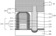
- FIG. 2 is a schematic structural diagram of a semiconductor structure provided by an embodiment of the present disclosure.
- the semiconductor structure includes: a substrate 200; a gate 210 located on part of the substrate 200, and the substrate 200 on both sides of the gate 210 has a source or drain; a dielectric layer 230 located on the substrate 200 , and the dielectric layer 230 covers the top surface and sidewall of the gate 210; the contact structure 220, the contact structure 220 penetrates the dielectric layer 230 and is electrically connected to the source or the drain; the first electrical connection part 240 and the second The electrical connection part 250, the first electrical connection part 240 and the second electrical connection part 250 are located on the top surface of the dielectric layer 230, and the second electrical connection part 250 is also in contact with part of the top surface of the contact structure 220, the first electrical connection part 240 Including the stacked first barrier layer 241 and the first conductive layer 242, in the direction along the direction from the source to the drain, the distance between the sidewall of the first barrier layer 241 facing the contact structure 220 and the contact structure 220 is the first The distance L 1 ,
- the process window for forming the first electrical connection portion 240 and the second electrical connection portion 250 is increased.
- the width dimension of the first conductive layer 242 is not changed, so that the first conductive layer 242 has a relatively large volume and low resistance, so that the first electrical connection portion 240 can maintain a good electrical conductivity.
- the semiconductor structure may be a memory, such as DRAM (Dynamic Random Access Memory), SRAM (Static Random-Access Memory, Static Random-Access Memory) or SDRAM (Synchronous Dynamic Random-Access Memory, Synchronous Dynamic Random-Access Memory).
- DRAM Dynamic Random Access Memory
- SRAM Static Random-Access Memory
- SDRAM Synchronous Dynamic Random-Access Memory
- the substrate 200 may be a semiconductor substrate or a silicon-on-insulator substrate. In some embodiments, the substrate 200 may be a silicon substrate. In some other embodiments, the substrate 200 may also be a germanium substrate, a silicon germanium substrate or a silicon carbide substrate.
- the gate 210 includes: a gate dielectric layer 211 , a gate conductive layer 212 and a gate capping layer 213 which are stacked in sequence.
- the gate conductive layer 212 may include a first gate conductive layer 214, a barrier layer 215, and a second gate conductive layer 216 stacked in sequence, and the barrier layer 215 can prevent the first gate conductive layer 214 from contacting the second gate conductive layer 216.
- the two gate conductive layers 216 are interdiffused, and the material of the first gate conductive layer 214 is a semiconductor material, and the material of the second gate conductive layer 216 is a metal material.
- the material of the first gate conductive layer 214 can be polysilicon
- the material of the barrier layer 215 can be titanium nitride
- the material of the second gate conductive layer 216 can be any one of tungsten, copper or aluminum. kind.
- the gate conductive layer can be a single-layer structure
- the material of the gate conductive layer can be semiconductor material or metal
- the semiconductor material can be polysilicon
- the metal material can be any one of tungsten, copper or aluminum.
- the gate capping layer 213 mainly plays the role of isolation and insulation, and the material of the gate capping layer 213 can be silicon oxide or silicon nitride.
- the semiconductor structure may further include: a first spacer layer 217, the first sidewall layer 217 covers the sidewall of the gate 210; a second sidewall layer 218, the second sidewall layer 218 covers the sidewall of the first sidewall layer 217, the gate pole 210 and part of the substrate 200 ; etch stop layer 219 covering the second spacer layer 218 .
- One side of the gate 210 has a source in the substrate 200, the other side of the gate 210 has a drain in the substrate 200, the bottom surface of the contact structure 220 is electrically connected to the source or the drain, and the top surface is connected to the second electrode.
- the connecting portion 250 is connected to form an electrical connection between the source or the drain and the second electrical connecting portion 250 .
- the semiconductor structure is a PMOS transistor, and the dopant ions of the source and drain are P-type ions; in other embodiments, the semiconductor structure is an NMOS transistor, and the dopant ions of the source and drain are For N-type ions.
- the dielectric layer 230 includes a first dielectric layer 231 and a second dielectric layer 232 stacked in sequence.
- the top of the first dielectric layer 231 may be flush with the top of the etch stop layer 219 for isolating the gate 210 from other conductive structures; the second dielectric layer 232 is higher than the top of the etch stop layer 219, at During the etching process, the second dielectric layer 232 on the top of the gate 210 can protect the gate 210 so that the gate 210 is not damaged.
- the top of the first dielectric layer may be higher than the top of the etch stop layer; in still some embodiments, the top of the first dielectric layer may be lower than the top of the etch stop layer.
- the density of the second dielectric layer 232 is greater than that of the first dielectric layer 231, so as to enhance the protection effect of the second dielectric layer 232 on the gate 210; in other embodiments, the second dielectric layer The density of 232 may also be equal to the density of the first dielectric layer 231 .
- the material of the first dielectric layer 231 may be silicon oxide, and the material of the second dielectric layer 232 may be silicon nitride or silicon oxynitride.
- the second electrical connection portion 250 is in contact with the contact structure 220, the first electrical connection portion 240 is adjacent to the contact structure 220, and is in contact with another contact structure (not shown) in the semiconductor structure, each connecting the substrate 200 The current draw in the two adjacent sources or drains.
- the first barrier layer 241 in the first electrical connection portion 240 covers the bottom surface of the first conductive layer 242 and is in contact with the surface of the dielectric layer 230 to prevent ions in the first conductive layer 242 from diffusing into the dielectric layer 230 .
- the width of the first barrier layer 241 is smaller than the width of the first conductive layer 242 .
- a void is formed among the bottom of the first conductive layer 242, the sidewall of the first barrier layer 241 facing the contact structure 220, and the top surface of the dielectric layer 230. Due to the existence of the void, the bottom of the first electrical connection part 240 and the The distance between the contact structures 220 is relatively large, thereby reducing the probability of contact between the first electrical connection portion 240 and the contact structures 220 , thereby reducing the risk of short circuit.
- the ratio of the width of the first barrier layer 241 to the width of the first conductive layer 242 is 0.5 ⁇ 0.9.
- the width of the first barrier layer 241 is smaller than the width of the first conductive layer 242 , so that the distance between the bottom of an electrical connection portion 240 and the contact structure 220 is larger.
- the contact area between the first barrier layer 241 and the first conductive layer 242 is large, so that the contact resistance between the first barrier layer 241 and the first conductive layer 242 is small, so that the first electrical connection part 240
- the internal current conduction capability is relatively good, so that the electrical conductivity of the first electrical connection part 240 remains relatively good.
- the material of the first barrier layer 241 may be TiN or TaN, and the material of the first conductive layer 242 may be tungsten.
- the function of the first barrier layer 241 is to prevent metal ions in the first conductive layer 242 from diffusing into the dielectric layer 230 .
- the material of the first barrier layer 241 may also be any one of Ta or Ti, and the material of the first conductive layer 242 may also be any one of copper or aluminum.
- the thickness of the first barrier layer 241 is smaller than the thickness of the first conductive layer 242 . It can be understood that, within this thickness range, the thickness of the first conductive layer 242 is relatively large, and the conductivity of the first conductive layer 242 is relatively strong, so that the overall resistance of the first electrical connection part 240 is relatively low. Small, it is beneficial to improve the conduction ability of the current.
- the orthographic projection of the first barrier layer 241 on the surface of the substrate 200 is located within the orthographic projection of the first conductive layer 242 on the surface of the substrate 200 . That is to say, the first barrier layer 241 is directly opposite to the first conductive layer 242 , and the width of the first barrier layer 241 is smaller than the width of the first conductive layer 242 in the direction from the source to the drain. It should be noted that, unless otherwise specified, all the widths mentioned below refer to the width in the direction from the source to the drain.
- the second electrical connection portion 250 may include a stacked second barrier layer 251 and a second conductive layer 252, the second barrier layer 251 is in contact with a part of the top surface of the contact structure 220; and the top surface of the contact structure 220 , the sidewall of the second barrier layer 251 and the bottom surface of the second conductive layer 252 enclose a cavity area.
- the second electrical connection part may also be a single-layer structure including only the second conductive layer.
- the second barrier layer 251 is in contact with part of the top surface of the contact structure 220 , that is, forms a dislocation connection structure.
- the advantage of adopting this connection method is that on the one hand, more electrical connections can be formed on the surface of the dielectric layer 230 with the same area, making full use of the space and improving the performance of the semiconductor structure; on the other hand, compared with the second
- the barrier layer 251 covers the entire top surface of the contact structure 220
- the existence of the part of the top surface of the contact structure 220 that is not connected to the second barrier layer 251 makes the relative relationship between the second electrical connection part 250 and the first electrical connection part 240 The distance is further increased to reduce the risk of short circuit between the first electrical connection part 240 and the second electrical connection part 250 .
- the sidewall of the second barrier layer 251 away from the contact structure 220 is indented to the right relative to the sidewall of the second conductive layer 252 away from the contact structure 220 , so that the second barrier layer 251
- the relative distance between the second barrier layer 251 and the first barrier layer 241 increases. That is, the width of the second barrier layer 251 is smaller than the width of the second conductive layer 252 . Therefore, the bottom of the second conductive layer 252 and the second barrier layer 251 can be kept away from the sidewall of the contact structure 220 and the contact structure 220 by only reducing the width of the second barrier layer 251 without changing the width of the second conductive layer 252.
- a cavity is formed between the top surfaces.
- the existence of the cavity makes it difficult for the adjacent first electrical connection part 240 and the second electrical connection part 250 to have a narrow contact and cause a short circuit, further reducing the risk of short circuit.
- the sidewall of the second barrier layer 251 facing the contact structure 220 is indented to the left relative to the sidewall of the second conductive layer 252 facing the contact structure 220, so that the bottom of the second electrical connection part 250 and the adjacent contact structure (not Shown) The distance between the tops is increased, reducing the probability of contact, thereby reducing the risk of short circuits.
- the sidewall of the second barrier layer facing the contact structure may also be flush with the sidewall of the second conductive layer facing the contact structure, as shown in FIG. 3 .
- the width of the first barrier layer 241 is equal to the width of the second barrier layer 251 along the direction from the source to the drain. This is because, in the specific process steps of forming the first barrier layer 241 and the second barrier layer 251, a one-step etching method is adopted, and the same process parameters are set to return the first barrier layer 241 and the second barrier layer 251. etch, so that the width of the first barrier layer 241 is equal to the width of the second barrier layer 251 . In this way, the process steps can be simplified, which is beneficial to large-scale production.
- the width of the first barrier layer 241 may not be equal to the width of the second barrier layer 251 along the direction from the source to the drain. It can be set that the sidewall of the first barrier layer 241 facing the contact structure 220 is indented to the right relative to the sidewall of the first conductive layer 242 facing the contact structure 220 and the sidewall away from the contact structure 220 is away from the contact structure relative to the first conductive layer 242 220 is indented to the left; the sidewall of the second barrier layer 251 facing the contact structure 220 is flush with the sidewall of the second conductive layer 252 facing the contact structure 220 , and the second barrier layer 251 is away from the sidewall of the contact structure 220 The sidewall of the second conductive layer 252 away from the contact structure 220 is indented to the right.
- the material of the first barrier layer 241 may be the same as that of the second barrier layer 251 ; the material of the first conductive layer 242 may be the same as that of the second conductive layer 252 .
- the width of the first barrier layer 241 is smaller than the width of the first conductive layer 242, and the width of the second barrier layer 251 is smaller than the width of the first barrier layer 251.
- the width of the second conductive layer 252, and in the direction along the direction from the source to the drain, the length of the first barrier layer 241 is equal to the width of the second barrier layer 251, which simplifies the process flow.
- the contact structure 220 runs through the entire dielectric layer 230 , and the width of the contact structure 220 located in the first dielectric layer 231 is greater than that of the contact structure 220 located in the second dielectric layer 232 , that is, a structure with a narrow top and a wide bottom is formed. This is because the second dielectric layer 232 has a higher density and is difficult to etch in an actual process, so the width of the contact structure 220 formed in the second dielectric layer 232 is smaller. It can be understood that, in some other embodiments, the width of the contact structure located in the first dielectric layer may also be equal to the width of the contact structure located in the second dielectric layer.
- the contact structure 220 includes: a conductive body part 221, the conductive body part 221 penetrates the dielectric layer 230, and the second electrical connection part 250 is in contact with a part of the surface of the conductive body part 221; a diffusion barrier layer 222, a diffusion barrier The layer 222 is located on the sidewall and the bottom of the conductive body portion 221 .
- the diffusion barrier layer 222 can prevent ions in the conductive body portion 221 from diffusing into the dielectric layer 230 and the substrate 200 .
- the top surface of the diffusion barrier layer 222 between the conductive body part 221 and the first electrical connection part 240 is lower than the top surface of the conductive body part 221, and the conductive body part 221, the dielectric layer 230 and the conductive body part 221 and the first electrical connection part
- the top surface of the diffusion barrier layer 222 between 240 forms a via area.
- the existence of the through hole region further increases the second distance between the first barrier layer 241 and the sidewall of the contact structure 220 compared with the condition without the through hole region. In this way, the risk of short circuit between the first electrical connection part 240 and the contact structure 220 is further reduced.
- the top surface of the diffusion barrier layer 222 between the conductive body portion 221 and the first electrical connection portion 240 may also be flush with the top surface of the conductive body portion 221 .
- the material of the diffusion barrier layer 222 is the same as that of the first barrier layer 241
- the material of the conductive body portion 221 is the same as that of the first conductive layer 242 .
- the material of the diffusion barrier layer 222 and the material of the first barrier layer 241 are both titanium nitride
- the material of the conductive body portion 221 and the material of the first conductive layer 242 are both tungsten.
- the material of the diffusion barrier layer 222 may also be different from that of the first barrier layer 241 , and the material of the conductive body portion 221 may also be different from that of the first conductive layer 242 .
- the material of the diffusion barrier layer 222 is titanium nitride
- the material of the first barrier layer 241 is tantalum nitride
- the material of the conductive body portion 221 is copper
- the material of the first conductive layer 242 is tungsten.
- the first electrical connection portion 240 includes a first barrier layer 241 and a first conductive layer 242 arranged in a stack, and the first barrier layer 241 faces the contact structure along the direction from the source to the drain.
- the distance between the sidewall of 220 and the contact structure 220 is the first distance L 1
- the distance between the sidewall of the first conductive layer 242 facing the contact structure 220 and the contact structure 220 is the second distance L 2
- the first distance L 1 is greater than the second distance L 2 . That is to say, the bottom profile of the first electrical connection part 240 is changed so that the distance between the first barrier layer 241 and the adjacent contact structure 220 is relatively large, and the first electrical connection part 240 and the second electrical connection are formed.
- the process of the part 250 avoid the problem that the distance between the first electrical connection part 240 and the contact structure 220 is relatively close due to the alignment deviation, thereby reducing the risk of a short circuit, and at the same time increasing the process of forming the first electrical connection part 240 and the second electrical connection part 240.
- the process window of the connecting portion 250 avoid the problem that the distance between the first electrical connection part 240 and the contact structure 220 is relatively close due to the alignment deviation, thereby reducing the risk of a short circuit, and at the same time increasing the process of forming the first electrical connection part 240 and the second electrical connection part 240.
- Another embodiment of the present disclosure provides a method for preparing a semiconductor structure.
- the method for preparing a semiconductor structure can form the semiconductor structure provided in the previous disclosed embodiment.
- the following will describe the preparation of the semiconductor structure provided by another embodiment of the present disclosure in conjunction with the accompanying drawings. The method is described in detail.
- 4 to 8 are structural schematic diagrams corresponding to each step in the method for manufacturing a semiconductor structure provided by another embodiment of the present disclosure.
- a substrate 200 and a gate 210 located on the substrate 200 are provided, and the substrate 200 on both sides of the gate 210 has a source or a drain, and the substrate 200 also has a dielectric layer 230, and the dielectric layer 230 covers the top surface and sidewalls of the gate 210 .
- the substrate 200 is a semiconductor substrate, and in some embodiments, the semiconductor substrate is a silicon substrate. In some other embodiments, the semiconductor substrate may also be a germanium substrate, a silicon germanium substrate or a silicon carbide substrate.
- the step of forming the gate 210 may include: forming a gate dielectric layer 211 , a gate conductive layer 212 and a gate capping layer 213 which are stacked in sequence.
- the gate conductive layer 212 may include a first gate conductive layer 214 , a barrier layer 215 and a second gate conductive layer 216 stacked in sequence.
- the semiconductor structure is a PMOS transistor, and the dopant ions of the source and drain are P-type ions; in other embodiments, the semiconductor structure is an NMOS transistor, and the dopant ions of the source and drain are For N-type ions.
- the step of forming the dielectric layer 230 includes: forming a first dielectric layer 231 and a second dielectric layer 232 stacked in sequence.
- the density of the second dielectric layer 232 is greater than that of the first dielectric layer 231 , so that the second dielectric layer 232 has a stronger protective effect on the gate 210 . In other embodiments, the density of the second dielectric layer 232 may also be equal to the density of the first dielectric layer 231 .
- a contact structure 220 is formed, and the contact structure 220 penetrates through the dielectric layer 230 and is electrically connected to the source or the drain.
- the specific process steps of forming the contact structure 220 include: patterning the first dielectric layer 231 and the second dielectric layer 232 by an etching process, and forming the first through hole 21 and the second through hole 22 that communicate with each other.
- the first through hole 21 penetrates the first dielectric layer 231
- the second through hole 22 penetrates the second dielectric layer 232
- the first through hole 21 and the second through hole 22 are facing and communicating, so that in the subsequent steps, the first through hole
- the first contact layer in the first through hole is directly opposite to and communicates with the second contact layer in the second through hole, so that the contact between the first contact layer and the second contact layer
- the contact area is larger, thereby reducing the contact resistance between the first contact layer and the second contact layer.
- first through hole 21 and the second through hole 22 are formed using the same etching process parameters.
- first dielectric layer 231 and the second dielectric layer 232 may also be etched respectively to form the first through hole 21 and the second through hole 22 .
- the width of the first through hole 21 is greater than the width of the second through hole 22, this is because the etching rate of the second dielectric layer 232 is lower than the etching rate of the first dielectric layer 231, relatively speaking, the second dielectric layer 232 is larger than the first dielectric layer 232 A dielectric layer 231 is dense, the etching rate of the first dielectric layer 231 is relatively fast, or the etching selectivity ratio of the etching process gas to the material of the second dielectric layer 232 is greater than the etching selectivity ratio of the material of the first dielectric layer 232 . Therefore, in a one-step etching process, a through-hole structure with a narrow top and a wide bottom is formed. It can be understood that, in some other embodiments, the width of the first through hole may also be equal to the width of the second through hole.
- the step of forming the contact structure 220 includes: forming a conductive body portion 221 in the via hole 20 and a diffusion barrier layer 222 located on the sidewall and bottom of the conductive body portion.
- the diffusion barrier layer 222 can prevent ions in the conductive body portion 221 from diffusing into the substrate 200 and the dielectric layer 230 .
- the material of the diffusion barrier layer 222 can be TiN or TaN, and the material of the conductive body part 221 can be W; in other embodiments, the material of the diffusion barrier layer 222 can also be any of Ta or Ti.
- the material of the conductive body part 221 may also be copper or aluminum.
- the specific process steps of forming the contact structure 220 are:
- the initial conductive main body is deposited on the surface of the diffusion barrier layer 222 in the first through hole 21 and the second through hole 22 by a deposition process, and the initial conductive main body is higher than the top surface of the dielectric layer 230; Part of the initial conductive body portion, and the remaining initial conductive body portion is used as the conductive body portion 221 to form the contact structure 220 .
- the contact structure 220 runs through the entire dielectric layer 230, and the width of the contact structure 220 located in the first dielectric layer 231 is greater than the width of the contact structure 220 located in the second dielectric layer 232, that is, a narrow top and a wide bottom are formed. structure. This is because the second dielectric layer 232 has a higher density and is difficult to etch in an actual process, so the width of the contact structure 220 formed in the second dielectric layer 232 is smaller.
- the width of the contact structure 220 in the first dielectric layer 231 is larger than that of the contact structure in the second dielectric layer 232 220 wide, so that the overall volume of the contact structure 220 increases, so it has a smaller resistance, thereby improving the current conduction capability. It can be understood that, in some other embodiments, the width of the contact structure located in the first dielectric layer may also be equal to the width of the contact structure located in the second dielectric layer.
- a metal silicide layer 225 may be formed at the bottom of the first through hole 21 , and the metal silicide layer 225 may reduce the contact resistance between the contact structure 220 and the source or drain.
- the material of the metal silicide layer 225 may be cobalt silicide.
- a first electrical connection portion 240 and a second electrical connection portion 250 arranged at intervals are formed, the first electrical connection portion 240 and the second electrical connection portion 250 are both formed on the top surface of the dielectric layer 230, and the second electrical connection The portion 250 is also in contact with part of the top surface of the contact structure 220.
- the first electrical connection portion 240 includes a stacked first barrier layer 241 and a first conductive layer 242.
- the first barrier layer In the direction along the direction from the source to the drain, the first barrier layer The distance between the sidewall of 241 facing the contact structure 220 and the contact structure 220 is the first distance L 1 , the distance between the sidewall of the first conductive layer 242 facing the contact structure 220 and the contact structure 220 is the second distance L 2 , The first distance L 1 is greater than the second distance L 2 .
- a cavity is formed between the bottom of the first conductive layer 242 , the sidewall of the first barrier layer 241 facing the contact structure 220 , and the top surface of the dielectric layer 230 .
- the distance between the structures 220 is increased, thereby reducing the probability of contact between the two structures, thereby reducing the possibility of short circuit.
- the first barrier layer 241 can prevent the ions in the first conductive layer 242 from diffusing into the medium layer 230 .
- the material of the first barrier layer 241 can be TiN or TaN, and the material of the first conductive layer 242 can be tungsten; in other embodiments, the material of the first barrier layer 241 can also be Any one of Ta or Ti, and the material of the first conductive layer 242 may also be any one of copper or aluminum.
- the process steps of forming the first electrical connection part 240 and the second electrical connection part 250 include:
- an initial barrier layer 31 and an initial conductive layer 32 are sequentially stacked on the top surface of the dielectric layer 230 , and the initial barrier layer 31 covers the top surface of the contact structure 220 .
- the initial conductive layer 32 and the initial barrier layer 31 are patterned to form a phase. Specifically, the initial barrier layer 31 and the initial conductive layer 32 are sequentially deposited on the top surface of the dielectric layer 230 by a deposition process.
- the initial conductive layer 32 and the initial barrier layer 31 are etched using a dry etching process. Before etching the initial conductive layer 32 and the initial barrier layer 31, it also includes: forming a patterned mask layer on the surface of the initial conductive layer 32, using the patterned mask layer as a mask, etching part of the initial conductive layer 32 and The initial barrier layer 31 until a part of the top surface of the contact structure 220 and a part of the top surface of the dielectric layer 230 are exposed. The exposed portion of the dielectric layer 230 can isolate the contact structure 220 from the first initial electrical connection portion 40 to prevent them from contacting and causing a short circuit.
- the exposed top surface of the contact structure 220 and the top surface of the dielectric layer 230 may be further etched to form a concave surface facing the substrate 200 . In this way, even in the case of low accuracy of etching parameters, the isolation effect can be achieved, and the process window for forming the first initial electrical connection portion 40 and the second electrical initial electrical connection portion can be enlarged.
- the top surface of the exposed contact structure and the top surface of the dielectric layer may not be etched continuously.
- the initial barrier layer 41 (refer to FIG. 8) in the first initial electrical connection portion 40 (refer to FIG. 8) is etched towards the sidewall of the contact structure 220, and the first initial electrical connection portion 40 (refer to FIG. 8)
- the remaining initial barrier layer 41 (see FIG. 8 ) forms the first barrier layer 241
- the initial conductive layer 42 (see FIG. 8 ) in the first initial electrical connection portion 40 (see FIG. 8 ) forms the first conductive layer 242 .
- a wet etching process may be used to etch the sidewalls of the initial barrier layer 41 .
- the initial barrier layer 41 is etched to make the initial barrier layer 41
- the distance between the sidewall of 41 facing the contact structure 220 and the contact structure 220 becomes larger, so as to avoid the problem of electrical connection between the first electrical connection portion 240 and the contact structure 220 to cause a short circuit.
- the process window for forming the first electrical connection part 240 and the second electrical connection part 250 is increased.
- the width dimension of the initial conductive layer 42 does not change, that is, the resistance of the initial conductive layer 42 does not change, therefore, its better conductivity can still be maintained.
- a cavity is formed between the bottom of the second conductive layer 252 of the second electrical connection portion 250 , the sidewall of the second barrier layer 251 of the second electrical connection portion 250 away from the contact structure 220 , and the top surface of the contact structure 220 ,
- the existence of the cavity makes it difficult for the adjacent first electrical connection part 240 and the second electrical connection part 250 to contact, further reducing the risk of short circuit.
- the sidewall of the initial barrier layer in the second electrical connection portion may not be etched.
- the exposed Diffusion barrier layer 221. in the process step of etching the sidewall of the barrier layer 41 (refer to FIG. 8 ) facing the contact structure 220 in the first initial electrical connection portion 40 (refer to FIG. 8 ), the exposed Diffusion barrier layer 221. Therefore, the conductive body portion 222 in the contact structure 220 , the dielectric layer 230 , and the top surface of the diffusion barrier layer 221 between the conductive body portion 222 and the first electrical connection portion 240 enclose a through hole area. The existence of the through hole region further increases the second distance between the first barrier layer 241 and the sidewall of the contact structure 220 compared with the condition that no through hole region is formed. In this way, the risk of short circuit between the first electrical connection part 240 and the contact structure 220 is greatly reduced. It can be understood that, in other embodiments, the exposed diffusion barrier layer may not be etched.
- the first barrier layer 241 in the first electrical connection part 240 is over-etched, so that the distance between the first barrier layer 241 and the side wall of the contact structure 220 is compared with the first The distance between the conductive layer 242 and the sidewall of the contact structure 220 is larger. That is to say, changing the bottom profile of the first electrical connection part 240 makes the distance between the first barrier layer 241 and the adjacent contact structure 220 relatively large, so that the two are not easy to contact.
- the process of forming the first electrical connection portion 240 and the second electrical connection portion 250 the problem of a short distance between the first electrical connection portion 240 and the contact structure 220 due to misalignment is avoided, thereby reducing the risk of a short circuit.
- the process window for forming the first electrical connection portion 240 and the second electrical connection portion 250 is increased.
- the semiconductor structure includes: a gate on the substrate, with source or drain on both sides of the gate; a dielectric layer on the substrate; a contact structure, the contact structure penetrates through the dielectric layer and is connected to the source or the drain.
- the drain is electrically connected; the first electrical connection part and the second electrical connection part are arranged at intervals, the first electrical connection part and the second electrical connection part are located on the top surface of the dielectric layer, and the second electrical connection part is in contact with part of the top surface of the contact structure , the first electrical connection part includes a first barrier layer and a first conductive layer stacked, and in the direction along the direction from the source to the drain, the distance between the sidewall of the first barrier layer facing the contact structure and the contact structure is the first Distance, the distance between the sidewall of the first conductive layer facing the contact structure and the contact structure is a second distance, and the first distance is greater than the second distance.
- Embodiments of the present disclosure are advantageous in reducing the risk of short circuits in semiconductor structures.
Landscapes
- Engineering & Computer Science (AREA)
- Physics & Mathematics (AREA)
- Condensed Matter Physics & Semiconductors (AREA)
- General Physics & Mathematics (AREA)
- Manufacturing & Machinery (AREA)
- Computer Hardware Design (AREA)
- Microelectronics & Electronic Packaging (AREA)
- Power Engineering (AREA)
- Internal Circuitry In Semiconductor Integrated Circuit Devices (AREA)
Abstract
Embodiments of the present application relate to the field of semiconductors, and in particular, to a semiconductor structure and a manufacturing method therefor. The semiconductor structure comprises: a gate located on a substrate, a source or a drain being provided on two sides of the gate; a dielectric layer located on the substrate; a contact structure which passes through the dielectric layer and is electrically connected to the source or the drain; a first electrical connection portion and a second electrical connection portion which are spaced from each other and are located on the top surface of the dielectric layer, the second electrical connection portion being in contact with part of the top surface of the contact structure, and the first electrical connection portion comprising a first barrier layer and a first conductive layer that are stacked. In a direction from the source to the drain, the distance between the side wall of the first barrier layer facing the contact structure and the contact structure is a first distance, and the distance between the side wall of the first conductive layer facing the contact structure and the contact structure is a second distance, wherein the first distance is greater than the second distance. The embodiments of the present application facilitate reduction of short-circuit risk of semiconductor structures.
Description
相关申请的交叉引用Cross References to Related Applications
本公开要求在2021年08月20日提交中国专利局、申请号为202110963300.X、申请名称为“半导体结构及其制备方法”的中国专利申请的优先权,其全部内容通过引用结合在本公开中。This disclosure claims the priority of a Chinese patent application with application number 202110963300.X and application title "Semiconductor Structure and Preparation Method" filed with the China Patent Office on August 20, 2021, the entire contents of which are incorporated by reference in this disclosure middle.
本公开实施例涉及但不限于一种半导体结构及其制备方法。Embodiments of the present disclosure relate to but are not limited to a semiconductor structure and a manufacturing method thereof.
存储器是一种常见的半导体结构,在存储器内部有许多微小的导电结构单元,比如,栅极、位线以及源漏极等。为了将这些微小导电结构引出来,通常会在导电结构上制备金属互连结构。A memory is a common semiconductor structure, and there are many tiny conductive structural units inside the memory, such as a gate, a bit line, and a source and a drain. In order to lead out these tiny conductive structures, metal interconnection structures are usually prepared on the conductive structures.
使用金属互联结构将导电结构引出,不仅可以提升存储器的工作速率,还能增加存储器的集成度。通常,在半导体结构中,会设置多个位于介质层中的接触结构以及与接触结构相连的电连接部作为金属互联结构。并且,每个金属互连结构间隔设置,将相互隔离的导电结构各自引出。Using the metal interconnection structure to lead out the conductive structure can not only increase the working speed of the memory, but also increase the integration of the memory. Generally, in a semiconductor structure, a plurality of contact structures located in a dielectric layer and electrical connections connected to the contact structures are provided as metal interconnection structures. Moreover, each metal interconnection structure is arranged at intervals to lead out the conductive structures isolated from each other.
然而,随着存储器体积越来越小,存储器内部的接触结构以及电连接部设置得越来越紧密,这容易造成半导体结构内部发生短路的问题。However, as the size of the memory becomes smaller and smaller, the contact structures and electrical connections inside the memory are arranged more and more closely, which easily causes the problem of short circuit inside the semiconductor structure.
发明内容Contents of the invention
本公开实施例一方面提供一种半导体结构,包括:衬底;位于部分衬底上的栅极,且栅极两侧的衬底内具有源极或漏极;位于衬底上的介质层,且介质层覆盖栅极的顶面和侧壁;接触结构,接触结构贯穿介质层并与源极或者漏极电连接;相间隔设置的第一电连接部以及第二电连接部,第一电连接部与第二电连接部均位于介质层顶面,且第二电连接部还与接触结构的部分顶面相接触,第一电连接部包括堆叠设置的第一阻挡层以及第一导电层,在沿源极指向漏极 的方向上,第一阻挡层朝向接触结构的侧壁与接触结构之间的距离为第一距离,第一导电层朝向接触结构的侧壁与接触结构之间的距离为第二距离,第一距离大于第二距离。An embodiment of the present disclosure provides a semiconductor structure, including: a substrate; a gate located on a part of the substrate, and the substrate on both sides of the gate has a source or a drain; a dielectric layer located on the substrate, And the dielectric layer covers the top surface and sidewall of the gate; the contact structure, the contact structure penetrates the dielectric layer and is electrically connected to the source or the drain; the first electrical connection part and the second electrical connection part arranged at intervals, the first electrical connection Both the connection part and the second electrical connection part are located on the top surface of the dielectric layer, and the second electrical connection part is also in contact with a part of the top surface of the contact structure. The first electrical connection part includes a stacked first barrier layer and a first conductive layer, In the direction from the source to the drain, the distance between the sidewall of the first barrier layer facing the contact structure and the contact structure is the first distance, and the distance between the sidewall of the first conductive layer facing the contact structure and the contact structure is the second distance, the first distance is greater than the second distance.
在一些实施例中,在沿所述源极指向所述漏极的方向上,所述第一阻挡层的宽度小于所述第一导电层的宽度。In some embodiments, in a direction along the direction from the source to the drain, the width of the first barrier layer is smaller than the width of the first conductive layer.
在一些实施例中,所述第一阻挡层的宽度与所述第一导电层的宽度的比值为0.5~0.9。In some embodiments, the ratio of the width of the first barrier layer to the width of the first conductive layer is 0.5˜0.9.
在一些实施例中,所述第一阻挡层的材料包括TiN或者TaN,所述第一导电层的材料包括W。In some embodiments, the material of the first barrier layer includes TiN or TaN, and the material of the first conductive layer includes W.
在一些实施例中,所述第一阻挡层的厚度小于所述第一导电层的厚度。In some embodiments, the thickness of the first barrier layer is smaller than the thickness of the first conductive layer.
在一些实施例中,所述第二电连接部包括堆叠设置的第二阻挡层以及第二导电层,所述第二阻挡层与所述接触结构的部分顶面相接触;且所述接触结构顶面、所述第二阻挡层侧壁以及所述第二导电层底面围成空洞区域。In some embodiments, the second electrical connection part includes a stacked second barrier layer and a second conductive layer, the second barrier layer is in contact with a part of the top surface of the contact structure; and the top surface of the contact structure The surface, the sidewall of the second barrier layer and the bottom surface of the second conductive layer enclose a cavity area.
在一些实施例中,在沿所述源极指向所述漏极的方向上,所述第一阻挡层的宽度等于所述第二阻挡层的宽度。In some embodiments, the width of the first barrier layer is equal to the width of the second barrier layer along the direction from the source to the drain.
在一些实施例中,所述第一阻挡层的材料与所述第二阻挡层的材料相同;所述第一导电层的材料与所述第二导电层的材料相同。In some embodiments, the material of the first barrier layer is the same as that of the second barrier layer; the material of the first conductive layer is the same as that of the second conductive layer.
在一些实施例中,所述第一阻挡层在所述衬底表面的正投影位于所述第一导电层在所述衬底表面的正投影内,且所述第一阻挡层在所述衬底表面的正投影面积小于所述第一导电层在所述衬底表面的正投影面积。In some embodiments, the orthographic projection of the first barrier layer on the substrate surface is located within the orthographic projection of the first conductive layer on the substrate surface, and the first barrier layer is located on the surface of the substrate. The orthographic area of the bottom surface is smaller than the orthographic area of the first conductive layer on the surface of the substrate.
在一些实施例中,所述接触结构包括:In some embodiments, the contact structure includes:
导电主体部,所述导电主体部贯穿所述介质层,且所述第二电连接部与所述导电主体部的部分表面相接触;a conductive body part, the conductive body part penetrates the dielectric layer, and the second electrical connection part is in contact with a part of the surface of the conductive body part;
扩散阻挡层,所述扩散阻挡层位于所述导电主体部的侧壁以及底部。A diffusion barrier layer, the diffusion barrier layer is located on the sidewall and the bottom of the conductive main body.
在一些实施例中,位于所述导电主体部与所述第一电连接部之间的所述扩散阻挡层顶面低于所述导电主体部顶面,且所述导电主体部、所述介质层以及位于所述导电主体部与所述第一电连接部之间的所述扩散阻挡层顶面围成通孔 区域。In some embodiments, the top surface of the diffusion barrier layer between the conductive body part and the first electrical connection part is lower than the top surface of the conductive body part, and the conductive body part, the medium layer and the top surface of the diffusion barrier layer between the conductive body portion and the first electrical connection portion encloses a via area.
在一些实施例中,所述扩散阻挡层的材料与所述第一阻挡层的材料相同。In some embodiments, the material of the diffusion barrier layer is the same as that of the first barrier layer.
根据本公开一些实施例,本公开实施例另一方面还提供一种半导体结构的制备方法,包括:提供衬底以及位于部分衬底上的栅极,栅极两侧的衬底内具有源极或漏极;衬底上还具有介质层,且介质层覆盖栅极的顶面和侧壁;形成接触结构,接触结构贯穿介质层并与源极或者漏极电连接;形成相间隔设置的第一电连接部以及第二电连接部,第一电连接部与第二电连接部均位于介质层顶面,且第二电连接部还与接触结构的部分顶面相接触,第一电连接部包括堆叠设置的第一阻挡层以及第一导电层,在沿源极指向漏极的方向上,第一阻挡层朝向接触结构的侧壁与接触结构之间的距离为第一距离,第一导电层朝向接触结构的侧壁与接触结构之间的距离为第二距离,第一距离大于第二距离。According to some embodiments of the present disclosure, on the other hand, the embodiments of the present disclosure also provide a method for fabricating a semiconductor structure, including: providing a substrate and a gate located on a part of the substrate, and source electrodes are provided in the substrate on both sides of the gate. or the drain; there is also a dielectric layer on the substrate, and the dielectric layer covers the top surface and sidewall of the gate; a contact structure is formed, the contact structure penetrates the dielectric layer and is electrically connected to the source or the drain; An electrical connection portion and a second electrical connection portion, the first electrical connection portion and the second electrical connection portion are both located on the top surface of the dielectric layer, and the second electrical connection portion is also in contact with part of the top surface of the contact structure, the first electrical connection portion Including the stacked first barrier layer and the first conductive layer, in the direction along the direction from the source to the drain, the distance between the side wall of the first barrier layer facing the contact structure and the contact structure is the first distance, the first conductive layer The distance between the sidewall of the layer facing the contact structure and the contact structure is a second distance, the first distance being greater than the second distance.
在一些实施例中,形成所述第一电连接部以及所述第二电连接部的工艺步骤包括:In some embodiments, the process steps of forming the first electrical connection part and the second electrical connection part include:
在所述介质层顶面形成依次堆叠的初始阻挡层以及初始导电层,所述初始阻挡层覆盖所述接触结构顶面;forming an initial barrier layer and an initial conductive layer stacked in sequence on the top surface of the dielectric layer, the initial barrier layer covering the top surface of the contact structure;
对所述初始导电层以及所述初始阻挡层进行图形化处理,形成相互间隔设置的第一初始电连接部以及第二初始电连接部,所述第二初始电连接部与所述接触结构的部分顶面相接触;patterning the initial conductive layer and the initial barrier layer to form a first initial electrical connection portion and a second initial electrical connection portion spaced apart from each other, the second initial electrical connection portion and the contact structure part of the top surface is in contact;
对所述第一初始电连接部中的所述初始阻挡层朝向所述接触结构的侧壁进行刻蚀处理,所述第一初始电连接部中剩余所述初始阻挡层作为第一阻挡层,所述第一初始电连接部中剩余所述初始导电层作为第一导电层。performing etching treatment on the sidewall of the initial barrier layer facing the contact structure in the first initial electrical connection part, the initial barrier layer remaining in the first initial electrical connection part as a first barrier layer, The initial conductive layer remains in the first initial electrical connection portion as the first conductive layer.
在一些实施例中,在对所述第一初始电连接部中的所述初始阻挡层朝向所述接触结构的侧壁进行刻蚀处理的工艺步骤中,还对所述第二电连接部中的所述初始阻挡层的侧壁进行刻蚀处理。In some embodiments, in the process step of etching the sidewall of the initial barrier layer facing the contact structure in the first initial electrical connection part, the The sidewall of the initial barrier layer is etched.
在一些实施例中,所述接触结构包括导电主体部以及位于所述导电主体部侧壁和底部的扩散阻挡层;在对所述第一初始电连接部中的所述初始阻挡层朝向所述接触结构的侧壁进行刻蚀处理的工艺步骤中,还刻蚀露出的所述扩散阻 挡层。In some embodiments, the contact structure includes a conductive body part and a diffusion barrier layer located on the sidewall and bottom of the conductive body part; the initial barrier layer in the first initial electrical connection part faces the In the process step of etching the sidewall of the contact structure, the exposed diffusion barrier layer is also etched.
一个或多个实施例通过与之对应的附图中的图片进行示例性说明,这些示例性说明并不构成对实施例的限定,除非有特别申明,附图中的图不构成比例限制。One or more embodiments are exemplified by corresponding pictures in the drawings, and these exemplifications are not construed as limiting the embodiments, unless otherwise stated, and the pictures in the drawings are not limited in scale.
图1为半导体结构的一种剖面结构示意图;FIG. 1 is a schematic cross-sectional structure diagram of a semiconductor structure;
图2为本公开一实施例提供的半导体结构的一种剖面结构示意图;FIG. 2 is a schematic cross-sectional structure diagram of a semiconductor structure provided by an embodiment of the present disclosure;
图3为本公开一实施例提供的半导体结构的另一种剖面结构示意图;3 is a schematic diagram of another cross-sectional structure of a semiconductor structure provided by an embodiment of the present disclosure;
图4至图8为本公开一实施例提供的半导体结构的制备方法中各步骤对应的结构示意图4 to 8 are structural schematic diagrams corresponding to each step in the method for preparing a semiconductor structure provided by an embodiment of the present disclosure.
由背景技术可知,现有技术存在相间隔设置的电连接部和接触结构之间容易短路的问题。It can be known from the background art that there is a problem in the prior art that short circuits are easy between the spaced apart electrical connection parts and contact structures.
分析发现,导致电连接部与接触结构之间容易短路的原因之一在于,电连接部和与其相邻的接触结构之间距离较小,使得电连接部的底部和与其相邻的接触结构的顶面容易发生短路现象。The analysis found that one of the reasons for the easy short circuit between the electrical connection part and the contact structure is that the distance between the electrical connection part and its adjacent contact structure is small, so that the bottom of the electrical connection part and its adjacent contact structure The top surface is prone to short circuits.
现结合一种半导体结构对上述问题的原因进行进一步分析,图1为一种半导体结构的结构示意图,参考图1,半导体结构包括:衬底100;位于部分衬底100上的栅极110以及位于栅极110表面的侧墙层117,栅极110包括栅介质层111、栅极导电层112以及栅极盖层113,且栅极110两侧的衬底100内具有源极或漏极;位于衬底100上的介质层130,且介质层130覆盖栅极110的顶面和侧壁;接触结构120,接触结构120贯穿介质层130并与源极或者漏极电连接;相间隔设置的第一电连接部140以及第二电连接部150,第一电连接部140与第二电连接部150均位于介质层130顶面,且第二电连接部150还与接触结构120的部分顶面相接触。The reason for the above problem is further analyzed in conjunction with a semiconductor structure. FIG. 1 is a schematic structural diagram of a semiconductor structure. Referring to FIG. 1, the semiconductor structure includes: a substrate 100; The side wall layer 117 on the surface of the gate 110, the gate 110 includes a gate dielectric layer 111, a gate conductive layer 112 and a gate capping layer 113, and there are sources or drains in the substrate 100 on both sides of the gate 110; The dielectric layer 130 on the substrate 100, and the dielectric layer 130 covers the top surface and sidewall of the gate 110; the contact structure 120, the contact structure 120 penetrates the dielectric layer 130 and is electrically connected to the source or the drain; An electrical connection portion 140 and a second electrical connection portion 150, the first electrical connection portion 140 and the second electrical connection portion 150 are located on the top surface of the dielectric layer 130, and the second electrical connection portion 150 is also in contact with part of the top surface of the contact structure 120 touch.
第二电连接部150与接触结构120的部分顶面相接触,第一电连接部140与另一接触结构(未图示)的部分顶面相连,将相隔离的源极或漏极分别引出。在形成第一电连接部140和第二电连接部150的工艺过程中,可能存在对准误差,导致接触结构120和第一电连接部140之间距离过小,使得接触结构120顶部与第一电连接部140底部之间容易发生短路现象。The second electrical connection part 150 is in contact with a part of the top surface of the contact structure 120 , and the first electrical connection part 140 is connected with a part of the top surface of another contact structure (not shown), leading out the isolated source or drain respectively. During the process of forming the first electrical connection part 140 and the second electrical connection part 150, there may be an alignment error, which causes the distance between the contact structure 120 and the first electrical connection part 140 to be too small, so that the top of the contact structure 120 is in contact with the second electrical connection part 150. A short circuit is likely to occur between the bottoms of an electrical connection portion 140 .
本公开实施例提供一种半导体结构,仅改变第一电连接部的底部轮廓,使第一阻挡层和接触结构之间的距离较大,避免在形成第一电连接部以及第二电连接部的工艺过程中,产生对准误差导致第一电连接部与接触结构距离过近的问题,从而降低发生短路的风险,增加了形成第一电连接部与第二电连接部的工艺窗口。An embodiment of the present disclosure provides a semiconductor structure, only changing the bottom profile of the first electrical connection part, so that the distance between the first barrier layer and the contact structure is larger, and avoiding the formation of the first electrical connection part and the second electrical connection part. During the process, alignment errors lead to the problem that the distance between the first electrical connection part and the contact structure is too close, thereby reducing the risk of short circuit and increasing the process window for forming the first electrical connection part and the second electrical connection part.
下面将结合附图对本公开的各实施例进行详细的阐述。然而,本领域的普通技术人员可以理解,在本公开各实施例中,为了使读者更好地理解本公开而提出了许多技术细节。但是,即使没有这些技术细节和基于以下各实施例的种种变化和修改,也可以实现本公开所要求保护的技术方案。Various embodiments of the present disclosure will be described in detail below with reference to the accompanying drawings. However, those skilled in the art can understand that in various embodiments of the present disclosure, many technical details are provided for readers to better understand the present disclosure. However, even without these technical details and various changes and modifications based on the following embodiments, the technical solutions claimed in the present disclosure can be realized.
图2为本公开一实施例提供的半导体结构的一种结构示意图。FIG. 2 is a schematic structural diagram of a semiconductor structure provided by an embodiment of the present disclosure.
参考图2,半导体结构包括:衬底200;位于部分衬底200上的栅极210,且栅极210两侧的衬底200内具有源极或漏极;位于衬底200上的介质层230,且介质层230覆盖栅极210的顶面和侧壁;接触结构220,接触结构220贯穿介质层230并与源极或者漏极电连接;相间隔设置的第一电连接部240以及第二电连接部250,第一电连接部240与第二电连接部250均位于介质层230顶面,且第二电连接部250还与接触结构220的部分顶面相接触,第一电连接部240包括堆叠设置的第一阻挡层241以及第一导电层242,在沿源极指向漏极的方向上,第一阻挡层241朝向接触结构220的侧壁与接触结构220之间的距离为第一距离L
1,第一导电层242朝向接触结构220的侧壁与接触结构220之间的距离为第二距离L
2,第一距离L
1大于第二距离L
2。
Referring to FIG. 2 , the semiconductor structure includes: a substrate 200; a gate 210 located on part of the substrate 200, and the substrate 200 on both sides of the gate 210 has a source or drain; a dielectric layer 230 located on the substrate 200 , and the dielectric layer 230 covers the top surface and sidewall of the gate 210; the contact structure 220, the contact structure 220 penetrates the dielectric layer 230 and is electrically connected to the source or the drain; the first electrical connection part 240 and the second The electrical connection part 250, the first electrical connection part 240 and the second electrical connection part 250 are located on the top surface of the dielectric layer 230, and the second electrical connection part 250 is also in contact with part of the top surface of the contact structure 220, the first electrical connection part 240 Including the stacked first barrier layer 241 and the first conductive layer 242, in the direction along the direction from the source to the drain, the distance between the sidewall of the first barrier layer 241 facing the contact structure 220 and the contact structure 220 is the first The distance L 1 , the distance between the sidewall of the first conductive layer 242 facing the contact structure 220 and the contact structure 220 is a second distance L 2 , and the first distance L 1 is greater than the second distance L 2 .
本实施例仅改变第一电连接部240的底部轮廓,使得第一阻挡层241和与其相邻的接触结构220之间的距离增大,因此两者不容易接触到,降低半导体 结构产生短路的风险。同时还增加了形成第一电连接部240与第二电连接部250的工艺窗口。此外,不改变第一导电层242的宽度尺寸,使得第一导电层242具有相对较大的体积和较小的电阻,因此可以使第一电连接部240保持较好的导电能力。In this embodiment, only the bottom profile of the first electrical connection portion 240 is changed, so that the distance between the first barrier layer 241 and the contact structure 220 adjacent to it is increased, so that the two are not easily contacted, and the possibility of a short circuit in the semiconductor structure is reduced. risk. At the same time, the process window for forming the first electrical connection portion 240 and the second electrical connection portion 250 is increased. In addition, the width dimension of the first conductive layer 242 is not changed, so that the first conductive layer 242 has a relatively large volume and low resistance, so that the first electrical connection portion 240 can maintain a good electrical conductivity.
半导体结构可以为存储器,例如为DRAM(动态随机存储器,Dynamic Random Access Memory)、SRAM(静态随机存储器,Static Random-Access Memory)或者SDRAM(同步动态随机存储器,Synchronous Dynamic Random-Access Memory)。The semiconductor structure may be a memory, such as DRAM (Dynamic Random Access Memory), SRAM (Static Random-Access Memory, Static Random-Access Memory) or SDRAM (Synchronous Dynamic Random-Access Memory, Synchronous Dynamic Random-Access Memory).
衬底200可以为半导体衬底或者绝缘体上的硅衬底。在一些实施例中,衬底200可以为硅衬底。在另一些实施例中,衬底200还可以为锗衬底、锗化硅衬底或者碳化硅衬底。The substrate 200 may be a semiconductor substrate or a silicon-on-insulator substrate. In some embodiments, the substrate 200 may be a silicon substrate. In some other embodiments, the substrate 200 may also be a germanium substrate, a silicon germanium substrate or a silicon carbide substrate.
栅极210包括:依次堆叠设置的栅介质层211、栅极导电层212以及栅极盖层213。在一些实施例中,栅极导电层212可以包括依次层叠的第一栅极导电层214、阻挡层215以及第二栅极导电层216,阻挡层215可以防止第一栅极导电层214与第二栅极导电层216之间的相互扩散,且第一栅极导电层214的材料为半导体材料,第二栅极导电层216的材料为金属材料。在一些实施例中,第一栅极导电层214的材料可以为多晶硅,阻挡层215的材料可以为氮化钛,第二栅极导电层216的材料可以为钨、铜或者铝中的任一种。The gate 210 includes: a gate dielectric layer 211 , a gate conductive layer 212 and a gate capping layer 213 which are stacked in sequence. In some embodiments, the gate conductive layer 212 may include a first gate conductive layer 214, a barrier layer 215, and a second gate conductive layer 216 stacked in sequence, and the barrier layer 215 can prevent the first gate conductive layer 214 from contacting the second gate conductive layer 216. The two gate conductive layers 216 are interdiffused, and the material of the first gate conductive layer 214 is a semiconductor material, and the material of the second gate conductive layer 216 is a metal material. In some embodiments, the material of the first gate conductive layer 214 can be polysilicon, the material of the barrier layer 215 can be titanium nitride, and the material of the second gate conductive layer 216 can be any one of tungsten, copper or aluminum. kind.
在另一些实施例中,栅极导电层可以为单层结构,栅极导电层的材料可以为半导体材料或者金属,半导体材料可以为多晶硅,金属材料可以为钨、铜或者铝中的任一种。In other embodiments, the gate conductive layer can be a single-layer structure, the material of the gate conductive layer can be semiconductor material or metal, the semiconductor material can be polysilicon, and the metal material can be any one of tungsten, copper or aluminum. .
栅极盖层213主要起隔离绝缘的作用,栅极盖层213的材料可以为氧化硅或者氮化硅。The gate capping layer 213 mainly plays the role of isolation and insulation, and the material of the gate capping layer 213 can be silicon oxide or silicon nitride.
半导体结构还可以包括:第一侧墙层217,第一侧墙层217覆盖栅极210侧壁;第二侧墙层218,第二侧墙层218覆盖第一侧墙层217侧壁、栅极210以及部分衬底200;刻蚀停止层219,覆盖第二侧墙层218。The semiconductor structure may further include: a first spacer layer 217, the first sidewall layer 217 covers the sidewall of the gate 210; a second sidewall layer 218, the second sidewall layer 218 covers the sidewall of the first sidewall layer 217, the gate pole 210 and part of the substrate 200 ; etch stop layer 219 covering the second spacer layer 218 .
栅极210的一侧衬底200内具有源极,栅极210的另一侧衬底200内具有 漏极,接触结构220的底面与源极或者漏极电性连接,顶面与第二电连接部250连接,使源极或者漏极与第二电连接部250形成电性连接。在一些实施例中,半导体结构为PMOS管,则源极和漏极的掺杂离子为P型离子;在另一些实施例中,半导体结构为NMOS管,则源极和漏极的掺杂离子为N型离子。One side of the gate 210 has a source in the substrate 200, the other side of the gate 210 has a drain in the substrate 200, the bottom surface of the contact structure 220 is electrically connected to the source or the drain, and the top surface is connected to the second electrode. The connecting portion 250 is connected to form an electrical connection between the source or the drain and the second electrical connecting portion 250 . In some embodiments, the semiconductor structure is a PMOS transistor, and the dopant ions of the source and drain are P-type ions; in other embodiments, the semiconductor structure is an NMOS transistor, and the dopant ions of the source and drain are For N-type ions.
介质层230包括依次堆叠的第一介质层231和第二介质层232。在一些实施例中,第一介质层231的顶部可以与刻蚀停止层219顶部平齐,用于隔离栅极210与其它导电结构;第二介质层232高于刻蚀停止层219顶部,在刻蚀工艺过程中,位于栅极210顶部的第二介质层232可以对栅极210提供保护作用,从而使得栅极210不受损坏。在另一些实施例中,第一介质层的顶部可以高于刻蚀停止层顶部;在又一些实施例中,第一介质层的顶部还可以低于刻蚀停止层顶部。The dielectric layer 230 includes a first dielectric layer 231 and a second dielectric layer 232 stacked in sequence. In some embodiments, the top of the first dielectric layer 231 may be flush with the top of the etch stop layer 219 for isolating the gate 210 from other conductive structures; the second dielectric layer 232 is higher than the top of the etch stop layer 219, at During the etching process, the second dielectric layer 232 on the top of the gate 210 can protect the gate 210 so that the gate 210 is not damaged. In some other embodiments, the top of the first dielectric layer may be higher than the top of the etch stop layer; in still some embodiments, the top of the first dielectric layer may be lower than the top of the etch stop layer.
在一些实施例中,第二介质层232的致密度大于第一介质层231的致密度,以加强第二介质层232对栅极210的保护效果;在另一些实施例中,第二介质层232的致密度也可以等于第一介质层231的致密度。In some embodiments, the density of the second dielectric layer 232 is greater than that of the first dielectric layer 231, so as to enhance the protection effect of the second dielectric layer 232 on the gate 210; in other embodiments, the second dielectric layer The density of 232 may also be equal to the density of the first dielectric layer 231 .
在一些实施例中,第一介质层231的材料可以为氧化硅,第二介质层232的材料可以为氮化硅或者氮氧化硅。In some embodiments, the material of the first dielectric layer 231 may be silicon oxide, and the material of the second dielectric layer 232 may be silicon nitride or silicon oxynitride.
第二电连接部250与接触结构220相接触,第一电连接部240与接触结构220相邻,且与半导体结构中的另一接触结构(未图示)相接触,各自将衬底200中的两个相邻的源极或者漏极中的电流引出。第一电连接部240中的第一阻挡层241覆盖第一导电层242的底部表面,并且与介质层230的表面相接触,可以防止第一导电层242中的离子扩散至介质层230中。The second electrical connection portion 250 is in contact with the contact structure 220, the first electrical connection portion 240 is adjacent to the contact structure 220, and is in contact with another contact structure (not shown) in the semiconductor structure, each connecting the substrate 200 The current draw in the two adjacent sources or drains. The first barrier layer 241 in the first electrical connection portion 240 covers the bottom surface of the first conductive layer 242 and is in contact with the surface of the dielectric layer 230 to prevent ions in the first conductive layer 242 from diffusing into the dielectric layer 230 .
在沿源极指向漏极的方向上,第一阻挡层241的宽度小于第一导电层242的宽度。如此,使得第一导电层242底部、第一阻挡层241朝向接触结构220的侧壁以及介质层230顶面这三者间形成了一个空洞,由于空洞的存在,第一电连接部240底部与接触结构220之间的距离较大,从而降低第一电连接部240与接触结构220接触的概率,进而减小短路的风险。In the direction along the direction from the source to the drain, the width of the first barrier layer 241 is smaller than the width of the first conductive layer 242 . In this way, a void is formed among the bottom of the first conductive layer 242, the sidewall of the first barrier layer 241 facing the contact structure 220, and the top surface of the dielectric layer 230. Due to the existence of the void, the bottom of the first electrical connection part 240 and the The distance between the contact structures 220 is relatively large, thereby reducing the probability of contact between the first electrical connection portion 240 and the contact structures 220 , thereby reducing the risk of short circuit.
具体的,在一些实施例中,第一阻挡层241的宽度与第一导电层242的宽 度的比值为0.5~0.9。在这个比值范围内,一方面使得第一阻挡层241的宽度相较于第一导电层242的宽度而言较小,使得一电连接部240底部与接触结构220之间的距离较大。另一方面,第一阻挡层241与第一导电层242之间的接触面积较大,使得第一阻挡层241与第一导电层242之间的接触电阻较小,从而第一电连接部240内部的电流导通能力较好,使得第一电连接部240的导电性能保持较好。Specifically, in some embodiments, the ratio of the width of the first barrier layer 241 to the width of the first conductive layer 242 is 0.5˜0.9. Within this ratio range, on the one hand, the width of the first barrier layer 241 is smaller than the width of the first conductive layer 242 , so that the distance between the bottom of an electrical connection portion 240 and the contact structure 220 is larger. On the other hand, the contact area between the first barrier layer 241 and the first conductive layer 242 is large, so that the contact resistance between the first barrier layer 241 and the first conductive layer 242 is small, so that the first electrical connection part 240 The internal current conduction capability is relatively good, so that the electrical conductivity of the first electrical connection part 240 remains relatively good.
第一阻挡层241的材料可以为TiN或者TaN,第一导电层242的材料可以为钨。第一阻挡层241的作用为防止第一导电层242中的金属离子扩散至介质层230中。The material of the first barrier layer 241 may be TiN or TaN, and the material of the first conductive layer 242 may be tungsten. The function of the first barrier layer 241 is to prevent metal ions in the first conductive layer 242 from diffusing into the dielectric layer 230 .
在另一些实施例中,第一阻挡层241的材料也可以为Ta或者Ti中的任一种,第一导电层242的材料也可以为铜或者铝中的任一种。In some other embodiments, the material of the first barrier layer 241 may also be any one of Ta or Ti, and the material of the first conductive layer 242 may also be any one of copper or aluminum.
第一阻挡层241的厚度小于第一导电层242的厚度。可以理解的是,在这个厚度范围内,第一导电层242的厚度相对较大,而第一导电层242的导电能力是较强的,如此,使得第一电连接部240的整体电阻相对较小,有利于改善电流的导通能力。The thickness of the first barrier layer 241 is smaller than the thickness of the first conductive layer 242 . It can be understood that, within this thickness range, the thickness of the first conductive layer 242 is relatively large, and the conductivity of the first conductive layer 242 is relatively strong, so that the overall resistance of the first electrical connection part 240 is relatively low. Small, it is beneficial to improve the conduction ability of the current.
第一阻挡层241在衬底200表面的正投影位于第一导电层242在衬底200表面的正投影内。也就是说,第一阻挡层241与第一导电层242是正对的,在源极指向漏极的方向上,第一阻挡层241的宽度小于第一导电层242的宽度。需要说明的是,如无特别说明,以下所有提到的宽度,都是指在源极指向漏极的方向上的宽度。The orthographic projection of the first barrier layer 241 on the surface of the substrate 200 is located within the orthographic projection of the first conductive layer 242 on the surface of the substrate 200 . That is to say, the first barrier layer 241 is directly opposite to the first conductive layer 242 , and the width of the first barrier layer 241 is smaller than the width of the first conductive layer 242 in the direction from the source to the drain. It should be noted that, unless otherwise specified, all the widths mentioned below refer to the width in the direction from the source to the drain.
在一些实施例中,第二电连接部250可以包括堆叠设置的第二阻挡层251以及第二导电层252,第二阻挡层251与接触结构220的部分顶面相接触;且接触结构220顶面、第二阻挡层251侧壁以及第二导电层252底面围成空洞区域。在另一些实施例中,第二电连接部也可以为仅包括第二导电层的单层结构。In some embodiments, the second electrical connection portion 250 may include a stacked second barrier layer 251 and a second conductive layer 252, the second barrier layer 251 is in contact with a part of the top surface of the contact structure 220; and the top surface of the contact structure 220 , the sidewall of the second barrier layer 251 and the bottom surface of the second conductive layer 252 enclose a cavity area. In some other embodiments, the second electrical connection part may also be a single-layer structure including only the second conductive layer.
第二阻挡层251与接触结构220的部分顶面相接触,即形成错位连接的结构。采用这种连接方式的好处是:一方面使得在相同面积的介质层230表面,可以形成数量更多的电连接部,充分利用空间,提高半导体结构的性能;另一 方面,相较于第二阻挡层251覆盖接触结构220的整个顶面而言,部分未与第二阻挡层251连接的接触结构220顶面的存在,使得第二电连接部250与第一电连接部240之间的相对距离较进一步增大,减小第一电连接部240与第二电连接部250之间的短路风险。The second barrier layer 251 is in contact with part of the top surface of the contact structure 220 , that is, forms a dislocation connection structure. The advantage of adopting this connection method is that on the one hand, more electrical connections can be formed on the surface of the dielectric layer 230 with the same area, making full use of the space and improving the performance of the semiconductor structure; on the other hand, compared with the second As far as the barrier layer 251 covers the entire top surface of the contact structure 220, the existence of the part of the top surface of the contact structure 220 that is not connected to the second barrier layer 251 makes the relative relationship between the second electrical connection part 250 and the first electrical connection part 240 The distance is further increased to reduce the risk of short circuit between the first electrical connection part 240 and the second electrical connection part 250 .
以第一连接部240指向第二连接部250的方向为左边,第二阻挡层251远离接触结构220的侧壁相对第二导电层252的远离接触结构220的侧壁向右缩进,使得第二阻挡层251与第一阻挡层241之间的相对距离增大。也就是说,第二阻挡层251的宽度小于第二导电层252的宽度。因此,可以通过仅减小第二阻挡层251的宽度,而不改变第二导电层252的宽度,使第二导电层252底部、第二阻挡层251远离接触结构220的侧壁以及接触结构220顶面之间形成了一个空洞,该空洞的存在,使相邻的第一电连接部240与第二电连接部250中容易产生窄接触而导致短路的部位不易碰到,进一步降低短路风险。此外,第二阻挡层251朝向接触结构220的侧壁相对第二导电层252的朝向接触结构220的侧壁向左缩进,使得第二电连接部250底部和与其相邻的接触结构(未图示)顶部之间的距离增大,减小接触的概率,从而降低短路风险。Taking the direction in which the first connecting portion 240 points to the second connecting portion 250 as the left side, the sidewall of the second barrier layer 251 away from the contact structure 220 is indented to the right relative to the sidewall of the second conductive layer 252 away from the contact structure 220 , so that the second barrier layer 251 The relative distance between the second barrier layer 251 and the first barrier layer 241 increases. That is, the width of the second barrier layer 251 is smaller than the width of the second conductive layer 252 . Therefore, the bottom of the second conductive layer 252 and the second barrier layer 251 can be kept away from the sidewall of the contact structure 220 and the contact structure 220 by only reducing the width of the second barrier layer 251 without changing the width of the second conductive layer 252. A cavity is formed between the top surfaces. The existence of the cavity makes it difficult for the adjacent first electrical connection part 240 and the second electrical connection part 250 to have a narrow contact and cause a short circuit, further reducing the risk of short circuit. In addition, the sidewall of the second barrier layer 251 facing the contact structure 220 is indented to the left relative to the sidewall of the second conductive layer 252 facing the contact structure 220, so that the bottom of the second electrical connection part 250 and the adjacent contact structure (not Shown) The distance between the tops is increased, reducing the probability of contact, thereby reducing the risk of short circuits.
可以理解的是,在另一些实施例中,第二阻挡层的朝向接触结构的侧壁也可以与第二导电层的朝向接触结构的侧壁平齐,如图3所示。It can be understood that, in some other embodiments, the sidewall of the second barrier layer facing the contact structure may also be flush with the sidewall of the second conductive layer facing the contact structure, as shown in FIG. 3 .
在一些实施例中,在沿源极指向漏极的方向上,第一阻挡层241的宽度等于第二阻挡层251的宽度。这是因为,在具体形成第一阻挡层241与第二阻挡层251的工艺步骤中,采用一步刻蚀的方法,且设置相同的工艺参数对第一阻挡层241以及第二阻挡层251进行回刻蚀,因此形成第一阻挡层241的宽度等于第二阻挡层251的宽度。如此,可以简化工艺步骤,利于规模化生产。In some embodiments, the width of the first barrier layer 241 is equal to the width of the second barrier layer 251 along the direction from the source to the drain. This is because, in the specific process steps of forming the first barrier layer 241 and the second barrier layer 251, a one-step etching method is adopted, and the same process parameters are set to return the first barrier layer 241 and the second barrier layer 251. etch, so that the width of the first barrier layer 241 is equal to the width of the second barrier layer 251 . In this way, the process steps can be simplified, which is beneficial to large-scale production.
在另一些实施例中,在沿所述源极指向所述漏极的方向上,第一阻挡层241的宽度也可以不等于第二阻挡层251的宽度。可以设置第一阻挡层241朝向接触结构220的侧壁相对第一导电层242的朝向接触结构220的侧壁向右缩进和远离接触结构220的侧壁相对第一导电层242的远离接触结构220的侧壁向左缩进;第二阻挡层251朝向接触结构220的侧壁相对第二导电层252的朝向接 触结构220的侧壁平齐,第二阻挡层251远离接触结构220的侧壁相对第二导电层252的远离接触结构220的侧壁向右缩进。In other embodiments, the width of the first barrier layer 241 may not be equal to the width of the second barrier layer 251 along the direction from the source to the drain. It can be set that the sidewall of the first barrier layer 241 facing the contact structure 220 is indented to the right relative to the sidewall of the first conductive layer 242 facing the contact structure 220 and the sidewall away from the contact structure 220 is away from the contact structure relative to the first conductive layer 242 220 is indented to the left; the sidewall of the second barrier layer 251 facing the contact structure 220 is flush with the sidewall of the second conductive layer 252 facing the contact structure 220 , and the second barrier layer 251 is away from the sidewall of the contact structure 220 The sidewall of the second conductive layer 252 away from the contact structure 220 is indented to the right.
在一些实施例中,第一阻挡层241的材料可以与第二阻挡层251的材料相同;第一导电层242的材料可以与第二导电层252的材料相同。如此,使得在实际工艺中,可以通过相同的工艺参数,在同一刻蚀步骤中,同时实现形成第一阻挡层241的宽度小于第一导电层242的宽度,第二阻挡层251的宽度小于第二导电层252的宽度,且在沿所述源极指向所述漏极的方向上,第一阻挡层241的长度等于第二阻挡层251的宽度,简化工艺流程。In some embodiments, the material of the first barrier layer 241 may be the same as that of the second barrier layer 251 ; the material of the first conductive layer 242 may be the same as that of the second conductive layer 252 . In this way, in the actual process, the width of the first barrier layer 241 is smaller than the width of the first conductive layer 242, and the width of the second barrier layer 251 is smaller than the width of the first barrier layer 251. The width of the second conductive layer 252, and in the direction along the direction from the source to the drain, the length of the first barrier layer 241 is equal to the width of the second barrier layer 251, which simplifies the process flow.
接触结构220贯穿整个介质层230,且位于第一介质层231中的接触结构220的宽度大于位于第二介质层232中的接触结构220的宽度,即形成上窄下宽的结构。这是由于第二介质层232的致密度较大,在实际工艺中,较难刻蚀,因此在第二介质层232中形成的接触结构220宽度较小。可以理解的是,在另一些实施例中,位于第一介质层中的接触结构的宽度也可以等于位于第二介质层中的接触结构的宽度。The contact structure 220 runs through the entire dielectric layer 230 , and the width of the contact structure 220 located in the first dielectric layer 231 is greater than that of the contact structure 220 located in the second dielectric layer 232 , that is, a structure with a narrow top and a wide bottom is formed. This is because the second dielectric layer 232 has a higher density and is difficult to etch in an actual process, so the width of the contact structure 220 formed in the second dielectric layer 232 is smaller. It can be understood that, in some other embodiments, the width of the contact structure located in the first dielectric layer may also be equal to the width of the contact structure located in the second dielectric layer.
在一些实施例中,接触结构220包括:导电主体部221,导电主体部221贯穿介质层230,且第二电连接部250与导电主体部221的部分表面相接触;扩散阻挡层222,扩散阻挡层222位于导电主体部221的侧壁以及底部。扩散阻挡层222可以阻挡导电主体部221中的离子扩散至介质层230以及衬底200中。In some embodiments, the contact structure 220 includes: a conductive body part 221, the conductive body part 221 penetrates the dielectric layer 230, and the second electrical connection part 250 is in contact with a part of the surface of the conductive body part 221; a diffusion barrier layer 222, a diffusion barrier The layer 222 is located on the sidewall and the bottom of the conductive body portion 221 . The diffusion barrier layer 222 can prevent ions in the conductive body portion 221 from diffusing into the dielectric layer 230 and the substrate 200 .
导电主体部221与第一电连接部240之间的扩散阻挡层222顶面低于导电主体部221顶面,且导电主体部221、介质层230以及位于导电主体部221与第一电连接部240之间的扩散阻挡层222顶面围成通孔区域。通孔区域的存在,使得第一阻挡层241与接触结构220侧壁之间的第二距离相较于没有通孔区域的条件下,进一步增大。如此,进一步地降低了第一电连接部240与接触结构220之间的短路风险。The top surface of the diffusion barrier layer 222 between the conductive body part 221 and the first electrical connection part 240 is lower than the top surface of the conductive body part 221, and the conductive body part 221, the dielectric layer 230 and the conductive body part 221 and the first electrical connection part The top surface of the diffusion barrier layer 222 between 240 forms a via area. The existence of the through hole region further increases the second distance between the first barrier layer 241 and the sidewall of the contact structure 220 compared with the condition without the through hole region. In this way, the risk of short circuit between the first electrical connection part 240 and the contact structure 220 is further reduced.
在另一些实施例中,如图3所示,导电主体部221与第一电连接部240之间的扩散阻挡层222顶面也可以与导电主体部221顶面平齐。In other embodiments, as shown in FIG. 3 , the top surface of the diffusion barrier layer 222 between the conductive body portion 221 and the first electrical connection portion 240 may also be flush with the top surface of the conductive body portion 221 .
在一些实施例中,扩散阻挡层222的材料与第一阻挡层241的材料相同,导电主体部221的材料与第一导电层242的材料相同。例如,扩散阻挡层222的材料与第一阻挡层241的材料均为氮化钛;导电主体部221的材料与第一导电层242的材料均为钨。In some embodiments, the material of the diffusion barrier layer 222 is the same as that of the first barrier layer 241 , and the material of the conductive body portion 221 is the same as that of the first conductive layer 242 . For example, the material of the diffusion barrier layer 222 and the material of the first barrier layer 241 are both titanium nitride; the material of the conductive body portion 221 and the material of the first conductive layer 242 are both tungsten.
在另一些实施例中,扩散阻挡层222的材料也可以与第一阻挡层241的材料不同,导电主体部221的材料也可以与第一导电层242的材料不同。例如,扩散阻挡层222的材料为氮化钛第一阻挡层241的材料为氮化钽;导电主体部221的材料为铜,第一导电层242的材料为钨。In some other embodiments, the material of the diffusion barrier layer 222 may also be different from that of the first barrier layer 241 , and the material of the conductive body portion 221 may also be different from that of the first conductive layer 242 . For example, the material of the diffusion barrier layer 222 is titanium nitride, the material of the first barrier layer 241 is tantalum nitride; the material of the conductive body portion 221 is copper, and the material of the first conductive layer 242 is tungsten.
上述实施例提供的半导体结构中,第一电连接部240包括堆叠设置的第一阻挡层241以及第一导电层242,在沿源极指向漏极的方向上,第一阻挡层241朝向接触结构220的侧壁与接触结构220之间的距离为第一距离L
1,第一导电层242朝向接触结构220的侧壁与接触结构220之间的距离为第二距离L
2,第一距离L
1大于第二距离L
2。也就是说,改变第一电连接部240的底部轮廓,使得第一阻挡层241和与其相邻的接触结构220之间的距离相对较大,在形成第一电连接部240以及第二电连接部250的工艺过程中,避免对准偏差导致第一电连接部240与接触结构220距离较近的问题,从而降低产生短路的风险,同时还增加了形成第一电连接部240以及第二电连接部250的工艺窗口。
In the semiconductor structure provided in the above embodiments, the first electrical connection portion 240 includes a first barrier layer 241 and a first conductive layer 242 arranged in a stack, and the first barrier layer 241 faces the contact structure along the direction from the source to the drain. The distance between the sidewall of 220 and the contact structure 220 is the first distance L 1 , the distance between the sidewall of the first conductive layer 242 facing the contact structure 220 and the contact structure 220 is the second distance L 2 , and the first distance L 1 is greater than the second distance L 2 . That is to say, the bottom profile of the first electrical connection part 240 is changed so that the distance between the first barrier layer 241 and the adjacent contact structure 220 is relatively large, and the first electrical connection part 240 and the second electrical connection are formed. During the process of the part 250, avoid the problem that the distance between the first electrical connection part 240 and the contact structure 220 is relatively close due to the alignment deviation, thereby reducing the risk of a short circuit, and at the same time increasing the process of forming the first electrical connection part 240 and the second electrical connection part 240. The process window of the connecting portion 250 .
本公开另一实施例提供一种半导体结构的制备方法,该半导体结构的制备方法可以形成上一公开实施例提供的半导体结构,以下将结合附图对本公开另一实施例提供的半导体结构的制备方法进行详细说明。Another embodiment of the present disclosure provides a method for preparing a semiconductor structure. The method for preparing a semiconductor structure can form the semiconductor structure provided in the previous disclosed embodiment. The following will describe the preparation of the semiconductor structure provided by another embodiment of the present disclosure in conjunction with the accompanying drawings. The method is described in detail.
图4至图8为本公开另一实施例提供的半导体结构的制备方法中各步骤对应的结构示意图。4 to 8 are structural schematic diagrams corresponding to each step in the method for manufacturing a semiconductor structure provided by another embodiment of the present disclosure.
参考图4,提供衬底200以及位于衬底200上的栅极210,且栅极210两侧的衬底200内具有源极或漏极,衬底200上还具有介质层230,且介质层230覆盖栅极210的顶面和侧壁。Referring to FIG. 4, a substrate 200 and a gate 210 located on the substrate 200 are provided, and the substrate 200 on both sides of the gate 210 has a source or a drain, and the substrate 200 also has a dielectric layer 230, and the dielectric layer 230 covers the top surface and sidewalls of the gate 210 .
衬底200为半导体衬底,在一些实施例中,半导体衬底为硅衬底。在另一些实施例中,半导体衬底还可以为锗衬底、锗化硅衬底或者碳化硅衬底。The substrate 200 is a semiconductor substrate, and in some embodiments, the semiconductor substrate is a silicon substrate. In some other embodiments, the semiconductor substrate may also be a germanium substrate, a silicon germanium substrate or a silicon carbide substrate.
形成栅极210的步骤可以包括:形成依次堆叠设置的栅介质层211、栅极导电层212以及栅极盖层213。在一些实施例中,栅极导电层212可以包括依次层叠的第一栅极导电层214、阻挡层215以及第二栅极导电层216。The step of forming the gate 210 may include: forming a gate dielectric layer 211 , a gate conductive layer 212 and a gate capping layer 213 which are stacked in sequence. In some embodiments, the gate conductive layer 212 may include a first gate conductive layer 214 , a barrier layer 215 and a second gate conductive layer 216 stacked in sequence.
还可以包括:形成第一侧墙层217,第一侧墙层217覆盖栅极210侧壁;形成第二侧墙层218,第二侧墙层218覆盖第一侧墙层217侧壁、栅极210以及部分衬底200;形成刻蚀停止层219,覆盖第二侧墙层218。It may also include: forming a first sidewall layer 217, the first sidewall layer 217 covers the sidewall of the grid 210; forming a second sidewall layer 218, the second sidewall layer 218 covers the sidewall of the first sidewall layer 217, the grid electrode 210 and part of the substrate 200 ; forming an etching stop layer 219 covering the second spacer layer 218 .
还包括:在栅极210的一侧衬底200内形成源极,栅极210的另一侧衬底200内形成漏极。在一些实施例中,半导体结构为PMOS管,则源极和漏极的掺杂离子为P型离子;在另一些实施例中,半导体结构为NMOS管,则源极和漏极的掺杂离子为N型离子。It also includes: forming a source in the substrate 200 on one side of the gate 210 , and forming a drain in the substrate 200 on the other side of the gate 210 . In some embodiments, the semiconductor structure is a PMOS transistor, and the dopant ions of the source and drain are P-type ions; in other embodiments, the semiconductor structure is an NMOS transistor, and the dopant ions of the source and drain are For N-type ions.
形成介质层230的步骤包括:形成依次堆叠的第一介质层231和第二介质层232。The step of forming the dielectric layer 230 includes: forming a first dielectric layer 231 and a second dielectric layer 232 stacked in sequence.
在一些实施例中,第二介质层232的致密度大于第一介质层231的致密度,使得第二介质层232对栅极210的保护作用增强。在另一些实施例中,第二介质层232的致密度也可以等于第一介质层231的致密度。In some embodiments, the density of the second dielectric layer 232 is greater than that of the first dielectric layer 231 , so that the second dielectric layer 232 has a stronger protective effect on the gate 210 . In other embodiments, the density of the second dielectric layer 232 may also be equal to the density of the first dielectric layer 231 .
有关衬底、栅极和介质层的详细说明,可参考前述实施例的具体描述,以下将不做详细赘述。For detailed descriptions of the substrate, the gate and the dielectric layer, reference may be made to the specific descriptions of the foregoing embodiments, which will not be described in detail below.
参考图5及图6,形成接触结构220,接触结构220贯穿介质层230并与源极或者漏极电连接。Referring to FIG. 5 and FIG. 6 , a contact structure 220 is formed, and the contact structure 220 penetrates through the dielectric layer 230 and is electrically connected to the source or the drain.
具体地,参考图5,形成接触结构220的具体工艺步骤包括:采用刻蚀工艺图形化第一介质层231和第二介质层232,形成相互连通的第一通孔21以及第二通孔22,第一通孔21贯穿第一介质层231,第二通孔22贯穿第二介质层232,且第一通孔21与第二通孔22正对且相通,使得后续步骤中在第一通孔与第二通孔中填充接触结构时,第一通孔中的第一接触层与第二通孔中的第二接触层正对且相通,从而使得第一接触层与第二接触层的接触面积较大,进而减小第一接触层与第二接触层的接触电阻。Specifically, referring to FIG. 5 , the specific process steps of forming the contact structure 220 include: patterning the first dielectric layer 231 and the second dielectric layer 232 by an etching process, and forming the first through hole 21 and the second through hole 22 that communicate with each other. , the first through hole 21 penetrates the first dielectric layer 231, the second through hole 22 penetrates the second dielectric layer 232, and the first through hole 21 and the second through hole 22 are facing and communicating, so that in the subsequent steps, the first through hole When the contact structure is filled in the hole and the second through hole, the first contact layer in the first through hole is directly opposite to and communicates with the second contact layer in the second through hole, so that the contact between the first contact layer and the second contact layer The contact area is larger, thereby reducing the contact resistance between the first contact layer and the second contact layer.
值得注意的是,在一些实施例中,在同一步骤中,采用相同的刻蚀工艺参 数形成第一通孔21以及第二通孔22。在另一些实施例中,也可以分别对第一介质层231以及第二介质层232进行刻蚀,形成第一通孔21以及第二通孔22。It should be noted that, in some embodiments, in the same step, the first through hole 21 and the second through hole 22 are formed using the same etching process parameters. In other embodiments, the first dielectric layer 231 and the second dielectric layer 232 may also be etched respectively to form the first through hole 21 and the second through hole 22 .
第一通孔21的宽度大于第二通孔22的宽度,这是因为第二介质层232刻蚀速率小于第一介质层231的刻蚀速率,相对而言,第二介质层232大与第一介质层231致密度,第一介质层231的刻蚀速率较快,或者刻蚀工艺气体对第二介质层232的材料的刻蚀选择比大于第一介质层232的材料的刻蚀选择比。因此,在一步刻蚀的工艺步骤中,形成了上窄下宽的通孔结构。可以理解的是,在另一些实施例中,第一通孔的宽度也可以等于第二通孔的宽度。The width of the first through hole 21 is greater than the width of the second through hole 22, this is because the etching rate of the second dielectric layer 232 is lower than the etching rate of the first dielectric layer 231, relatively speaking, the second dielectric layer 232 is larger than the first dielectric layer 232 A dielectric layer 231 is dense, the etching rate of the first dielectric layer 231 is relatively fast, or the etching selectivity ratio of the etching process gas to the material of the second dielectric layer 232 is greater than the etching selectivity ratio of the material of the first dielectric layer 232 . Therefore, in a one-step etching process, a through-hole structure with a narrow top and a wide bottom is formed. It can be understood that, in some other embodiments, the width of the first through hole may also be equal to the width of the second through hole.
参考图6,形成接触结构220的步骤包括:在通孔20中形成导电主体部221以及位于导电主体部侧壁和底部的扩散阻挡层222。扩散阻挡层222可以阻挡导电主体部221中的离子扩散至衬底200以及介质层230中。Referring to FIG. 6 , the step of forming the contact structure 220 includes: forming a conductive body portion 221 in the via hole 20 and a diffusion barrier layer 222 located on the sidewall and bottom of the conductive body portion. The diffusion barrier layer 222 can prevent ions in the conductive body portion 221 from diffusing into the substrate 200 and the dielectric layer 230 .
在一些实施例中,扩散阻挡层222的材料可以为TiN或者TaN,导电主体部221的材料可以为W;在另一些实施例中,扩散阻挡层222的材料还可以为Ta或者Ti中的任一种,导电主体部221的材料还可以为铜或者铝。In some embodiments, the material of the diffusion barrier layer 222 can be TiN or TaN, and the material of the conductive body part 221 can be W; in other embodiments, the material of the diffusion barrier layer 222 can also be any of Ta or Ti. One, the material of the conductive body part 221 may also be copper or aluminum.
具体地,形成接触结构220的具体工艺步骤为:Specifically, the specific process steps of forming the contact structure 220 are:
采用沉积工艺在第一通孔21以及第二通孔22中沉积初始扩散阻挡层,且初始扩散阻挡层高于介质层230顶面;去除高于介质层230顶面的部分初始扩散阻挡层,剩余部分初始扩散阻挡层作为扩散阻挡层222;Depositing an initial diffusion barrier layer in the first through hole 21 and the second through hole 22 by using a deposition process, and the initial diffusion barrier layer is higher than the top surface of the dielectric layer 230; removing part of the initial diffusion barrier layer higher than the top surface of the dielectric layer 230, The rest of the initial diffusion barrier layer is used as the diffusion barrier layer 222;
采用沉积工艺在第一通孔21以及第二通孔22中的扩散阻挡层222表面沉积初始导电主体部,且初始导电主体部高于介质层230顶面;去除高于介质层230顶面的部分初始导电主体部,剩余初始导电主体部作为导电主体部221,形成接触结构220。The initial conductive main body is deposited on the surface of the diffusion barrier layer 222 in the first through hole 21 and the second through hole 22 by a deposition process, and the initial conductive main body is higher than the top surface of the dielectric layer 230; Part of the initial conductive body portion, and the remaining initial conductive body portion is used as the conductive body portion 221 to form the contact structure 220 .
在一些实施例中,接触结构220贯穿整个介质层230,位于第一介质层231中的接触结构220的宽度大于位于第二介质层232中的接触结构220的宽度,即形成上窄下宽的结构。这是由于第二介质层232的致密度较大,在实际工艺中,较难刻蚀,因此在第二介质层232中形成的接触结构220宽度较小。相较于第一介质层231中的接触结构220宽度等于第二介质层232中的接触结构220 宽度而言,第一介质层231中的接触结构220宽度大于第二介质层232中的接触结构220宽度,使得接触结构220整体的体积增大,因此具有更小的电阻,从而改善电流导通能力。可以理解的是,在另一些实施例中,位于第一介质层中的接触结构的宽度也可以等于位于第二介质层中的接触结构的宽度。In some embodiments, the contact structure 220 runs through the entire dielectric layer 230, and the width of the contact structure 220 located in the first dielectric layer 231 is greater than the width of the contact structure 220 located in the second dielectric layer 232, that is, a narrow top and a wide bottom are formed. structure. This is because the second dielectric layer 232 has a higher density and is difficult to etch in an actual process, so the width of the contact structure 220 formed in the second dielectric layer 232 is smaller. Compared with the width of the contact structure 220 in the first dielectric layer 231 being equal to the width of the contact structure 220 in the second dielectric layer 232, the width of the contact structure 220 in the first dielectric layer 231 is larger than that of the contact structure in the second dielectric layer 232 220 wide, so that the overall volume of the contact structure 220 increases, so it has a smaller resistance, thereby improving the current conduction capability. It can be understood that, in some other embodiments, the width of the contact structure located in the first dielectric layer may also be equal to the width of the contact structure located in the second dielectric layer.
在一些实施例中,在形成接触结构220之前,还可以在第一通孔21底部形成金属硅化层225,金属硅化层225可以减小接触结构220与源极或者漏极之间的接触电阻。具体地,金属硅化层225的材料可以是硅化钴。In some embodiments, before forming the contact structure 220 , a metal silicide layer 225 may be formed at the bottom of the first through hole 21 , and the metal silicide layer 225 may reduce the contact resistance between the contact structure 220 and the source or drain. Specifically, the material of the metal silicide layer 225 may be cobalt silicide.
参考图2,形成相间隔设置的第一电连接部240以及第二电连接部250,第一电连接部240与第二电连接部250均形成于介质层230顶面,且第二电连接部250还与接触结构220的部分顶面相接触,第一电连接部240包括堆叠设置的第一阻挡层241以及第一导电层242,在沿源极指向漏极的方向上,第一阻挡层241朝向接触结构220的侧壁与接触结构220之间的距离为第一距离L
1,第一导电层242朝向接触结构220的侧壁与接触结构220之间的距离为第二距离L
2,第一距离L
1大于第二距离L
2。
Referring to FIG. 2, a first electrical connection portion 240 and a second electrical connection portion 250 arranged at intervals are formed, the first electrical connection portion 240 and the second electrical connection portion 250 are both formed on the top surface of the dielectric layer 230, and the second electrical connection The portion 250 is also in contact with part of the top surface of the contact structure 220. The first electrical connection portion 240 includes a stacked first barrier layer 241 and a first conductive layer 242. In the direction along the direction from the source to the drain, the first barrier layer The distance between the sidewall of 241 facing the contact structure 220 and the contact structure 220 is the first distance L 1 , the distance between the sidewall of the first conductive layer 242 facing the contact structure 220 and the contact structure 220 is the second distance L 2 , The first distance L 1 is greater than the second distance L 2 .
也就是说,第一导电层242底部、第一阻挡层241朝向接触结构220的侧壁以及介质层230顶面三者间形成一个空洞,该空洞的存在使得第一电连接部240底部与接触结构220之间的距离增加,从而降低二者接触的概率,进而减小短路的可能。That is to say, a cavity is formed between the bottom of the first conductive layer 242 , the sidewall of the first barrier layer 241 facing the contact structure 220 , and the top surface of the dielectric layer 230 . The distance between the structures 220 is increased, thereby reducing the probability of contact between the two structures, thereby reducing the possibility of short circuit.
第一阻挡层241可以阻挡第一导电层242中的离子扩散至介质层230中。具体地,在一些实施例中,第一阻挡层241的材料可以为TiN或者TaN,第一导电层242的材料可以为钨;在另一些实施例中,第一阻挡层241的材料也可以为Ta或者Ti中的任一种,第一导电层242的材料也可以为铜或者铝中的任一种。The first barrier layer 241 can prevent the ions in the first conductive layer 242 from diffusing into the medium layer 230 . Specifically, in some embodiments, the material of the first barrier layer 241 can be TiN or TaN, and the material of the first conductive layer 242 can be tungsten; in other embodiments, the material of the first barrier layer 241 can also be Any one of Ta or Ti, and the material of the first conductive layer 242 may also be any one of copper or aluminum.
形成第一电连接部240以及第二电连接部250的工艺步骤包括:The process steps of forming the first electrical connection part 240 and the second electrical connection part 250 include:
参考图7,在介质层230顶面形成依次堆叠的初始阻挡层31以及初始导电层32,初始阻挡层31覆盖接触结构220顶面。Referring to FIG. 7 , an initial barrier layer 31 and an initial conductive layer 32 are sequentially stacked on the top surface of the dielectric layer 230 , and the initial barrier layer 31 covers the top surface of the contact structure 220 .
参考图8,对初始导电层32以及初始阻挡层31进行图形化处理,形成相 具体地,采用沉积工艺在介质层230顶面依次沉积初始阻挡层31以及初始导电层32。Referring to FIG. 8 , the initial conductive layer 32 and the initial barrier layer 31 are patterned to form a phase. Specifically, the initial barrier layer 31 and the initial conductive layer 32 are sequentially deposited on the top surface of the dielectric layer 230 by a deposition process.
互间隔设置的第一初始电连接部40以及第二初始电连接部50,第二初始电连接部50与接触结构220的部分顶面相接触;The first initial electrical connection part 40 and the second initial electrical connection part 50 arranged at intervals, the second initial electrical connection part 50 is in contact with part of the top surface of the contact structure 220;
采用干法刻蚀工艺,对初始导电层32以及初始阻挡层31进行刻蚀。在刻蚀初始导电层32以及初始阻挡层31之前,还包括:在初始导电层32表面形成图形化的掩膜层,以图形化的掩膜层为掩膜,刻蚀部分初始导电层32以及初始阻挡层31,直至露出部分接触结构220的顶面以及部分介质层230顶面。露出表面部分的介质层230可以隔离接触结构220与第一初始电连接部40,防止它们发生接触而产生短路。The initial conductive layer 32 and the initial barrier layer 31 are etched using a dry etching process. Before etching the initial conductive layer 32 and the initial barrier layer 31, it also includes: forming a patterned mask layer on the surface of the initial conductive layer 32, using the patterned mask layer as a mask, etching part of the initial conductive layer 32 and The initial barrier layer 31 until a part of the top surface of the contact structure 220 and a part of the top surface of the dielectric layer 230 are exposed. The exposed portion of the dielectric layer 230 can isolate the contact structure 220 from the first initial electrical connection portion 40 to prevent them from contacting and causing a short circuit.
在一些实施例中,还可以对露出表面的接触结构220顶面以及介质层230顶面继续刻蚀,形成一个朝向衬底200的凹面。如此,即使在刻蚀参数精确度较低的情况下,也可以达到隔离效果,增大形成第一初始电连接部40以及第二电初始电连接部的工艺窗口。In some embodiments, the exposed top surface of the contact structure 220 and the top surface of the dielectric layer 230 may be further etched to form a concave surface facing the substrate 200 . In this way, even in the case of low accuracy of etching parameters, the isolation effect can be achieved, and the process window for forming the first initial electrical connection portion 40 and the second electrical initial electrical connection portion can be enlarged.
可以理解的是,在另一些实施例中,也可以不对露出表面的接触结构顶面以及介质层顶面继续刻蚀。It can be understood that, in some other embodiments, the top surface of the exposed contact structure and the top surface of the dielectric layer may not be etched continuously.
参考图2,对第一初始电连接部40(参考图8)中的初始阻挡层41(参考图8)朝向接触结构220的侧壁进行刻蚀处理,第一初始电连接部40(参考图8)中剩余初始阻挡层41(参考图8)形成第一阻挡层241,第一初始电连接部40(参考图8)中初始导电层42(参考图8)形成第一导电层242。2, the initial barrier layer 41 (refer to FIG. 8) in the first initial electrical connection portion 40 (refer to FIG. 8) is etched towards the sidewall of the contact structure 220, and the first initial electrical connection portion 40 (refer to FIG. 8) The remaining initial barrier layer 41 (see FIG. 8 ) forms the first barrier layer 241 , and the initial conductive layer 42 (see FIG. 8 ) in the first initial electrical connection portion 40 (see FIG. 8 ) forms the first conductive layer 242 .
可以采用湿法刻蚀工艺,对初始阻挡层41的侧壁进行刻蚀处理。A wet etching process may be used to etch the sidewalls of the initial barrier layer 41 .
仅对初始阻挡层41进行刻蚀处理,改变第一初始电连接部40的底部轮廓,使第一电连接部240底部与接触结构220侧壁之间的距离相对较大,减小第一电连接部240与接触结构220侧壁接触而导致的短路风险。同时,在刻蚀工艺中可能存在对准偏差,使得初始阻挡层41与接触结构220侧壁之间距离过近甚至相接触,此时,对初始阻挡层41进行刻蚀处理,使初始阻挡层41朝向接触结构220的侧壁相对接触结构220之间的距离变大,避免第一电连接部240与 接触结构220产生电连接而短路的问题。如此,可以避免刻蚀工艺的对准偏差而导致第一电连接部240与接触结构220之间产生距离过近的问题,降低了第一电连接部240与接触结构220之间的短路风险,从而增加了形成第一电连接部240以及第二电连接部250的工艺窗口。此外,不改变初始导电层42的宽度尺寸,即初始导电层42的电阻不变,因此,仍能保持其较好的导电能力。Only the initial barrier layer 41 is etched to change the bottom profile of the first initial electrical connection portion 40, so that the distance between the bottom of the first electrical connection portion 240 and the side wall of the contact structure 220 is relatively large, reducing the first electrical connection. The risk of short circuit caused by the contact between the connecting portion 240 and the sidewall of the contact structure 220 . At the same time, there may be misalignment during the etching process, so that the distance between the initial barrier layer 41 and the sidewall of the contact structure 220 is too close or even in contact. At this time, the initial barrier layer 41 is etched to make the initial barrier layer 41 The distance between the sidewall of 41 facing the contact structure 220 and the contact structure 220 becomes larger, so as to avoid the problem of electrical connection between the first electrical connection portion 240 and the contact structure 220 to cause a short circuit. In this way, the problem of too close distance between the first electrical connection part 240 and the contact structure 220 caused by the alignment deviation of the etching process can be avoided, and the risk of short circuit between the first electrical connection part 240 and the contact structure 220 is reduced. Thus, the process window for forming the first electrical connection part 240 and the second electrical connection part 250 is increased. In addition, the width dimension of the initial conductive layer 42 does not change, that is, the resistance of the initial conductive layer 42 does not change, therefore, its better conductivity can still be maintained.
在一些实施例中,在对所述第一初始电连接部40(参考图8)中的初始阻挡层41(参考图8)朝向接触结构220的侧壁进行刻蚀处理的工艺步骤中,还对第二初始电连接部50(参考图8)中的初始阻挡层51(参考图8)的侧壁进行刻蚀处理。也就是说,第二电连接部250的第二导电层252底部、第二电连接部250的第二阻挡层251远离接触结构220的侧壁以及接触结构220顶面之间形成了一个空洞,该空洞的存在,使相邻的第一电连接部240与第二电连接部250不易接触,进一步降低短路风险。可以理解的是,在另一些实施例中,也可以不对第二电连接部中的初始阻挡层的侧壁进行刻蚀处理。In some embodiments, in the process step of etching the sidewall of the initial barrier layer 41 (refer to FIG. 8 ) facing the contact structure 220 in the first initial electrical connection portion 40 (refer to FIG. 8 ), further Etching treatment is performed on the sidewall of the initial barrier layer 51 (refer to FIG. 8 ) in the second initial electrical connection portion 50 (refer to FIG. 8 ). That is to say, a cavity is formed between the bottom of the second conductive layer 252 of the second electrical connection portion 250 , the sidewall of the second barrier layer 251 of the second electrical connection portion 250 away from the contact structure 220 , and the top surface of the contact structure 220 , The existence of the cavity makes it difficult for the adjacent first electrical connection part 240 and the second electrical connection part 250 to contact, further reducing the risk of short circuit. It can be understood that, in other embodiments, the sidewall of the initial barrier layer in the second electrical connection portion may not be etched.
在一些实施例中,在对第一初始电连接部40(参考图8)中的阻挡层41(参考图8)朝向接触结构220的侧壁进行刻蚀处理的工艺步骤中,还刻蚀露出的扩散阻挡层221。因此,接触结构220中的导电主体部222、介质层230以及位于导电主体部222与第一电连接部240之间的扩散阻挡层221顶面围成通孔区域。该通孔区域的存在,使得第一阻挡层241与接触结构220侧壁之间的第二距离较不形成通孔区域的条件下进一步增大。如此,更大的降低了第一电连接部240与接触结构220之间的短路风险。可以理解的是,在另一些实施例中,也可以不对露出的扩散阻挡层进行刻蚀。In some embodiments, in the process step of etching the sidewall of the barrier layer 41 (refer to FIG. 8 ) facing the contact structure 220 in the first initial electrical connection portion 40 (refer to FIG. 8 ), the exposed Diffusion barrier layer 221. Therefore, the conductive body portion 222 in the contact structure 220 , the dielectric layer 230 , and the top surface of the diffusion barrier layer 221 between the conductive body portion 222 and the first electrical connection portion 240 enclose a through hole area. The existence of the through hole region further increases the second distance between the first barrier layer 241 and the sidewall of the contact structure 220 compared with the condition that no through hole region is formed. In this way, the risk of short circuit between the first electrical connection part 240 and the contact structure 220 is greatly reduced. It can be understood that, in other embodiments, the exposed diffusion barrier layer may not be etched.
上述公开实施例提供的半导体结构的制备方法,对第一电连接部240中的第一阻挡层241进行过刻蚀,使得第一阻挡层241与接触结构220侧壁的距离相较于第一导电层242与接触结构220侧壁之间的距离更大。也就是说,改变第一电连接部240的底部轮廓,使得第一阻挡层241和与其相邻的接触结构220之间的距离相对较大,因此两者不容易接触到。在形成第一电连接部240以及第二电连接部250的工艺过程中,避免对准偏差导致第一电连接部240与接触 结构220距离较近的问题,从而降低发生短路的风险。同时还增加了形成第一电连接部240以及第二电连接部250的工艺窗口。In the manufacturing method of the semiconductor structure provided by the above disclosed embodiments, the first barrier layer 241 in the first electrical connection part 240 is over-etched, so that the distance between the first barrier layer 241 and the side wall of the contact structure 220 is compared with the first The distance between the conductive layer 242 and the sidewall of the contact structure 220 is larger. That is to say, changing the bottom profile of the first electrical connection part 240 makes the distance between the first barrier layer 241 and the adjacent contact structure 220 relatively large, so that the two are not easy to contact. During the process of forming the first electrical connection portion 240 and the second electrical connection portion 250 , the problem of a short distance between the first electrical connection portion 240 and the contact structure 220 due to misalignment is avoided, thereby reducing the risk of a short circuit. At the same time, the process window for forming the first electrical connection portion 240 and the second electrical connection portion 250 is increased.
本领域的普通技术人员可以理解,上述各实施方式是实现本公开的具体实施例,而在实际应用中,可以在形式上和细节上对其作各种改变,而不偏离本公开的精神和范围。任何本领域技术人员,在不脱离本公开的精神和范围内,均可作各自更动与修改,因此本公开的保护范围应当以权利要求限定的范围为准。Those of ordinary skill in the art can understand that the above-mentioned embodiments are specific examples for realizing the present disclosure, and in practical applications, various changes can be made in form and details without departing from the spirit and spirit of the present disclosure. scope. Any person skilled in the art can make respective alterations and modifications without departing from the spirit and scope of the present disclosure. Therefore, the protection scope of the present disclosure should be determined by the scope defined in the claims.
本公开实施例中,半导体结构包括:位于衬底上的栅极,栅极两侧具有源极或漏极;位于衬底上的介质层;接触结构,接触结构贯穿介质层并与源极或漏极电连接;间隔设置的第一电连接部和第二电连接部,第一电连接部与第二电连接部位于介质层顶面,第二电连接部与接触结构的部分顶面接触,第一电连接部包括堆叠设置的第一阻挡层和第一导电层,在沿源极指向漏极的方向上,第一阻挡层朝向接触结构的侧壁与接触结构间的距离为第一距离,第一导电层朝向接触结构的侧壁与接触结构间的距离为第二距离,第一距离大于第二距离。本公开申请实施例有利于降低半导体结构的短路风险。In the embodiment of the present disclosure, the semiconductor structure includes: a gate on the substrate, with source or drain on both sides of the gate; a dielectric layer on the substrate; a contact structure, the contact structure penetrates through the dielectric layer and is connected to the source or the drain. The drain is electrically connected; the first electrical connection part and the second electrical connection part are arranged at intervals, the first electrical connection part and the second electrical connection part are located on the top surface of the dielectric layer, and the second electrical connection part is in contact with part of the top surface of the contact structure , the first electrical connection part includes a first barrier layer and a first conductive layer stacked, and in the direction along the direction from the source to the drain, the distance between the sidewall of the first barrier layer facing the contact structure and the contact structure is the first Distance, the distance between the sidewall of the first conductive layer facing the contact structure and the contact structure is a second distance, and the first distance is greater than the second distance. Embodiments of the present disclosure are advantageous in reducing the risk of short circuits in semiconductor structures.
Claims (16)
- 一种半导体结构,包括:A semiconductor structure comprising:衬底;位于部分所述衬底上的栅极,且位于所述栅极两侧的所述衬底内具有源极或漏极;位于所述衬底上的介质层,且所述介质层覆盖所述栅极的表面;a substrate; a gate located on part of the substrate, and the substrate located on both sides of the gate has a source or a drain; a dielectric layer located on the substrate, and the dielectric layer covering the surface of the grid;接触结构,所述接触结构贯穿所述介质层并与所述源极或者所述漏极电连接;a contact structure, the contact structure penetrates through the dielectric layer and is electrically connected to the source or the drain;相间隔设置的第一电连接部以及第二电连接部,所述第一电连接部与所述第二电连接部均位于所述介质层顶面,且所述第二电连接部还与所述接触结构的部分顶面相接触,所述第一电连接部包括堆叠设置的第一阻挡层以及第一导电层,在沿所述源极指向所述漏极的方向上,所述第一阻挡层朝向所述接触结构的侧壁与所述接触结构之间的距离为第一距离,所述第一导电层朝向所述接触结构的侧壁与所述接触结构之间的距离为第二距离,所述第一距离大于所述第二距离。A first electrical connection part and a second electrical connection part arranged at intervals, the first electrical connection part and the second electrical connection part are located on the top surface of the dielectric layer, and the second electrical connection part is also connected to the Part of the top surface of the contact structure is in contact, the first electrical connection part includes a stacked first barrier layer and a first conductive layer, and in a direction along the direction from the source to the drain, the first The distance between the sidewall of the barrier layer facing the contact structure and the contact structure is a first distance, and the distance between the sidewall of the first conductive layer facing the contact structure and the contact structure is a second distance. distance, the first distance is greater than the second distance.
- 根据权利要求1所述的半导体结构,其中,在沿所述源极指向所述漏极的方向上,所述第一阻挡层的宽度小于所述第一导电层的宽度。The semiconductor structure according to claim 1, wherein, in a direction along the direction from the source to the drain, the width of the first barrier layer is smaller than the width of the first conductive layer.
- 根据权利要求2所述的半导体结构,其中,所述第一阻挡层的宽度与所述第一导电层的宽度的比值为0.5~0.9。The semiconductor structure according to claim 2, wherein a ratio of a width of the first barrier layer to a width of the first conductive layer is 0.5˜0.9.
- 根据权利要求1所述的半导体结构,其中,所述第一阻挡层的材料包括TiN或者TaN,所述第一导电层的材料包括W。The semiconductor structure according to claim 1, wherein the material of the first barrier layer comprises TiN or TaN, and the material of the first conductive layer comprises W.
- 根据权利要求1所述的半导体结构,其中,所述第一阻挡层的厚度小于所述第一导电层的厚度。The semiconductor structure of claim 1, wherein the thickness of the first barrier layer is less than the thickness of the first conductive layer.
- 根据权利要求1所述的半导体结构,其中,所述第二电连接部包括堆叠设置的第二阻挡层以及第二导电层,所述第二阻挡层与所述接触结构的部分顶面相接触;且所述接触结构顶面、所述第二阻挡层侧壁以及所述第二导电层底面围成空洞区域。The semiconductor structure according to claim 1, wherein the second electrical connection part comprises a second barrier layer and a second conductive layer arranged in a stack, the second barrier layer is in contact with part of the top surface of the contact structure; And the top surface of the contact structure, the sidewall of the second barrier layer and the bottom surface of the second conductive layer enclose a cavity area.
- 根据权利要求6所述的半导体结构,其中,在沿所述源极指向所述漏极 的方向上,所述第一阻挡层的宽度等于所述第二阻挡层的宽度。The semiconductor structure according to claim 6, wherein, in a direction along the direction from the source to the drain, the width of the first barrier layer is equal to the width of the second barrier layer.
- 根据权利要求6所述的半导体结构,其中,所述第一阻挡层的材料与所述第二阻挡层的材料相同;所述第一导电层的材料与所述第二导电层的材料相同。The semiconductor structure according to claim 6, wherein the material of the first barrier layer is the same as that of the second barrier layer; the material of the first conductive layer is the same as that of the second conductive layer.
- 根据权利要求1所述的半导体结构,其中,所述第一阻挡层在所述衬底表面的正投影位于所述第一导电层在所述衬底表面的正投影内,且所述第一阻挡层在所述衬底表面的正投影面积小于所述第一导电层在所述衬底表面的正投影面积。The semiconductor structure according to claim 1, wherein the orthographic projection of the first barrier layer on the substrate surface is located within the orthographic projection of the first conductive layer on the substrate surface, and the first The orthographic area of the blocking layer on the surface of the substrate is smaller than the area of the orthographic projection of the first conductive layer on the surface of the substrate.
- 根据权利要求1所述的半导体结构,其中,所述接触结构包括:The semiconductor structure of claim 1, wherein the contact structure comprises:导电主体部,所述导电主体部贯穿所述介质层,且所述第二电连接部与所述导电主体部的部分表面相接触;a conductive body part, the conductive body part penetrates the dielectric layer, and the second electrical connection part is in contact with a part of the surface of the conductive body part;扩散阻挡层,所述扩散阻挡层位于所述导电主体部的侧壁以及底部。A diffusion barrier layer, the diffusion barrier layer is located on the sidewall and the bottom of the conductive main body.
- 根据权利要求10所述的半导体结构,其中,位于所述导电主体部与所述第一电连接部之间的所述扩散阻挡层顶面低于所述导电主体部顶面,且所述导电主体部、所述介质层以及位于所述导电主体部与所述第一电连接部之间的所述扩散阻挡层顶面围成通孔区域。The semiconductor structure according to claim 10, wherein the top surface of the diffusion barrier layer between the conductive body portion and the first electrical connection portion is lower than the top surface of the conductive body portion, and the conductive body portion The main body, the dielectric layer, and the top surface of the diffusion barrier layer between the conductive main body and the first electrical connection portion enclose a through hole area.
- 根据权利要求10所述的半导体结构,其中,所述扩散阻挡层的材料与所述第一阻挡层的材料相同。The semiconductor structure of claim 10, wherein the material of the diffusion barrier layer is the same as the material of the first barrier layer.
- 一种半导体结构的制备方法,包括:A method for preparing a semiconductor structure, comprising:提供衬底以及位于部分所述衬底上的栅极,且位于所述栅极两侧的所述衬底内具有源极或漏极;所述衬底上还具有介质层,且所述介质层覆盖所述栅极的表面;Provide a substrate and a gate on part of the substrate, and the substrate on both sides of the gate has a source or a drain; there is also a dielectric layer on the substrate, and the dielectric a layer covering the surface of the gate;形成接触结构,所述接触结构贯穿所述介质层并与所述源极或者所述漏极电连接;forming a contact structure, the contact structure penetrating through the dielectric layer and electrically connected to the source or the drain;形成相间隔设置的第一电连接部以及第二电连接部,所述第一电连接部与所述第二电连接部均位于所述介质层顶面,且所述第二电连接部还与所述接触结构的部分顶面相接触,所述第一电连接部包括堆叠设置的第一阻挡层以及第 一导电层,在沿所述源极指向所述漏极的方向上,所述第一阻挡层朝向所述接触结构的侧壁与所述接触结构之间的距离为第一距离,所述第一导电层朝向所述接触结构的侧壁与所述接触结构之间的距离为第二距离,所述第一距离大于所述第二距离。Forming a first electrical connection part and a second electrical connection part arranged at intervals, the first electrical connection part and the second electrical connection part are both located on the top surface of the dielectric layer, and the second electrical connection part is also In contact with a part of the top surface of the contact structure, the first electrical connection part includes a stacked first barrier layer and a first conductive layer, and in a direction along the direction from the source to the drain, the first A distance between a side wall of the barrier layer facing the contact structure and the contact structure is a first distance, and a distance between the side wall of the first conductive layer facing the contact structure and the contact structure is a first distance. Two distances, the first distance is greater than the second distance.
- 根据权利要求13所述的半导体结构的制备方法,其中,形成所述第一电连接部以及所述第二电连接部的工艺步骤包括:The method for manufacturing a semiconductor structure according to claim 13, wherein the process step of forming the first electrical connection part and the second electrical connection part comprises:在所述介质层顶面形成依次堆叠的初始阻挡层以及初始导电层,所述初始阻挡层覆盖所述接触结构顶面;forming an initial barrier layer and an initial conductive layer stacked in sequence on the top surface of the dielectric layer, the initial barrier layer covering the top surface of the contact structure;对所述初始导电层以及所述初始阻挡层进行图形化处理,形成相互间隔设置的第一初始电连接部以及第二初始电连接部,所述第二初始电连接部与所述接触结构的部分顶面相接触;patterning the initial conductive layer and the initial barrier layer to form a first initial electrical connection portion and a second initial electrical connection portion spaced apart from each other, the second initial electrical connection portion and the contact structure part of the top surface is in contact;对所述第一初始电连接部中的所述初始阻挡层朝向所述接触结构的侧壁进行刻蚀处理,所述第一初始电连接部中剩余所述初始阻挡层作为第一阻挡层,所述第一初始电连接部中剩余所述初始导电层作为第一导电层。performing etching treatment on the sidewall of the initial barrier layer facing the contact structure in the first initial electrical connection part, the initial barrier layer remaining in the first initial electrical connection part as a first barrier layer, The initial conductive layer remains in the first initial electrical connection portion as the first conductive layer.
- 根据权利要求14所述的半导体结构的制备方法,其中,在对所述第一初始电连接部中的所述初始阻挡层朝向所述接触结构的侧壁进行刻蚀处理的工艺步骤中,还对所述第二电连接部中的所述初始阻挡层的侧壁进行刻蚀处理。The method for fabricating a semiconductor structure according to claim 14, wherein, in the process step of etching the sidewall of the initial barrier layer facing the contact structure in the first initial electrical connection part, further Etching is performed on the sidewall of the initial barrier layer in the second electrical connection portion.
- 根据权利要求14所述的半导体结构的制备方法,其中,所述接触结构包括导电主体部以及位于所述导电主体部侧壁和底部的扩散阻挡层;在对所述第一初始电连接部中的所述初始阻挡层朝向所述接触结构的侧壁进行刻蚀处理的工艺步骤中,还刻蚀露出的所述扩散阻挡层。The method for fabricating a semiconductor structure according to claim 14, wherein the contact structure comprises a conductive body part and a diffusion barrier layer located on the sidewall and bottom of the conductive body part; in the first initial electrical connection part In the process step of etching the sidewall of the initial barrier layer facing the contact structure, the exposed diffusion barrier layer is also etched.
Priority Applications (2)
| Application Number | Priority Date | Filing Date | Title |
|---|---|---|---|
| EP22715962.1A EP4160664A1 (en) | 2021-08-20 | 2022-01-17 | Semiconductor structure and manufacturing method therefor |
| US17/708,281 US20230055307A1 (en) | 2021-08-20 | 2022-03-30 | Semiconductor structure and method for preparing same |
Applications Claiming Priority (2)
| Application Number | Priority Date | Filing Date | Title |
|---|---|---|---|
| CN202110963300.X | 2021-08-20 | ||
| CN202110963300.XA CN115843175A (en) | 2021-08-20 | 2021-08-20 | Semiconductor structure and preparation method thereof |
Related Child Applications (1)
| Application Number | Title | Priority Date | Filing Date |
|---|---|---|---|
| US17/708,281 Continuation US20230055307A1 (en) | 2021-08-20 | 2022-03-30 | Semiconductor structure and method for preparing same |
Publications (1)
| Publication Number | Publication Date |
|---|---|
| WO2023019880A1 true WO2023019880A1 (en) | 2023-02-23 |
Family
ID=82196416
Family Applications (1)
| Application Number | Title | Priority Date | Filing Date |
|---|---|---|---|
| PCT/CN2022/072283 WO2023019880A1 (en) | 2021-08-20 | 2022-01-17 | Semiconductor structure and manufacturing method therefor |
Country Status (3)
| Country | Link |
|---|---|
| CN (1) | CN115843175A (en) |
| TW (1) | TWI829193B (en) |
| WO (1) | WO2023019880A1 (en) |
Citations (5)
| Publication number | Priority date | Publication date | Assignee | Title |
|---|---|---|---|---|
| CN1246727A (en) * | 1998-08-31 | 2000-03-08 | 株式会社日立制作所 | Manufacture technology of semiconductor integrated circuit device |
| US6528368B1 (en) * | 2002-02-26 | 2003-03-04 | Samsung Electronics Co., Ltd. | Method for fabricating semiconductor device, and semiconductor device, having storage node contact flugs |
| JP2010267987A (en) * | 2010-07-12 | 2010-11-25 | Renesas Electronics Corp | Semiconductor device and method of manufacturing the same |
| CN102024784A (en) * | 2009-09-22 | 2011-04-20 | 台湾积体电路制造股份有限公司 | Block contact plugs for mos devices |
| CN108811517A (en) * | 2017-02-28 | 2018-11-13 | 桑迪士克科技有限责任公司 | High-voltage field effect transistor with the gate-dielectric being laterally extended and its manufacturing method |
Family Cites Families (4)
| Publication number | Priority date | Publication date | Assignee | Title |
|---|---|---|---|---|
| US7381642B2 (en) * | 2004-09-23 | 2008-06-03 | Megica Corporation | Top layers of metal for integrated circuits |
| US6607980B2 (en) * | 2001-02-12 | 2003-08-19 | Symetrix Corporation | Rapid-temperature pulsing anneal method at low temperature for fabricating layered superlattice materials and making electronic devices including same |
| US11107923B2 (en) * | 2019-06-14 | 2021-08-31 | Taiwan Semiconductor Manufacturing Company, Ltd. | Source/drain regions of FinFET devices and methods of forming same |
| US11121225B2 (en) * | 2019-11-01 | 2021-09-14 | Taiwan Semiconductor Manufacturing Company, Ltd. | Field plate structure to enhance transistor breakdown voltage |
-
2021
- 2021-08-20 CN CN202110963300.XA patent/CN115843175A/en active Pending
-
2022
- 2022-01-17 WO PCT/CN2022/072283 patent/WO2023019880A1/en unknown
- 2022-06-10 TW TW111121591A patent/TWI829193B/en active
Patent Citations (5)
| Publication number | Priority date | Publication date | Assignee | Title |
|---|---|---|---|---|
| CN1246727A (en) * | 1998-08-31 | 2000-03-08 | 株式会社日立制作所 | Manufacture technology of semiconductor integrated circuit device |
| US6528368B1 (en) * | 2002-02-26 | 2003-03-04 | Samsung Electronics Co., Ltd. | Method for fabricating semiconductor device, and semiconductor device, having storage node contact flugs |
| CN102024784A (en) * | 2009-09-22 | 2011-04-20 | 台湾积体电路制造股份有限公司 | Block contact plugs for mos devices |
| JP2010267987A (en) * | 2010-07-12 | 2010-11-25 | Renesas Electronics Corp | Semiconductor device and method of manufacturing the same |
| CN108811517A (en) * | 2017-02-28 | 2018-11-13 | 桑迪士克科技有限责任公司 | High-voltage field effect transistor with the gate-dielectric being laterally extended and its manufacturing method |
Also Published As
| Publication number | Publication date |
|---|---|
| TW202310338A (en) | 2023-03-01 |
| CN115843175A (en) | 2023-03-24 |
| TWI829193B (en) | 2024-01-11 |
Similar Documents
| Publication | Publication Date | Title |
|---|---|---|
| KR100665852B1 (en) | Method for manufacturing semiconductor device | |
| CN110896075B (en) | Integrated circuit memory and preparation method thereof | |
| KR970003953A (en) | Highly Integrated DRAM Cells and Manufacturing Method Thereof | |
| TWI802469B (en) | Storage device and method for forming storage device | |
| KR20220148366A (en) | Semiconductor Device | |
| WO2022148067A1 (en) | Semiconductor structure and manufacturing method therefor | |
| WO2023019880A1 (en) | Semiconductor structure and manufacturing method therefor | |
| US20220238665A1 (en) | Semiconductor structure and formation method thereof | |
| US11688783B1 (en) | Semiconductor device and method for manufacturing the same | |
| WO2022041981A1 (en) | Semiconductor structure and method for manufacturing semiconductor structure | |
| US20220130840A1 (en) | Semiconductor structure and semiconductor structure manufacturing method | |
| US20230055307A1 (en) | Semiconductor structure and method for preparing same | |
| TW202224147A (en) | Semiconductor memory device | |
| WO2023015844A1 (en) | Semiconductor structure and preparation method therefor | |
| KR20230016875A (en) | Semiconductor device and method for fabricating the same | |
| US20080211018A1 (en) | Semiconductor device and method of manufacturing the same | |
| KR20070093794A (en) | Method for forming contact plug in semiconductor device | |
| US20230042793A1 (en) | Semiconductor structure and method for manufacturing same | |
| KR20210013811A (en) | Semiconductor device | |
| US20230040132A1 (en) | Method of manufacturing semiconductor device | |
| WO2022088850A1 (en) | Semiconductor structure and method for fabricating semiconductor structure | |
| WO2022052593A1 (en) | Semiconductor device and manufacturing method therefor | |
| TWI817356B (en) | Semiconductor device and method for manufacturing the same | |
| US11895830B2 (en) | Method for manufacturing semiconductor device | |
| WO2023133941A1 (en) | Semiconductor structure and manufacturing method therefor |
Legal Events
| Date | Code | Title | Description |
|---|---|---|---|
| ENP | Entry into the national phase |
Ref document number: 2022715962 Country of ref document: EP Effective date: 20220421 |
|
| NENP | Non-entry into the national phase |
Ref country code: DE |