WO2023013659A1 - 異原子ドープナノダイヤモンド粒子及び異原子ドープナノダイヤモンド粒子の製造方法 - Google Patents
異原子ドープナノダイヤモンド粒子及び異原子ドープナノダイヤモンド粒子の製造方法 Download PDFInfo
- Publication number
- WO2023013659A1 WO2023013659A1 PCT/JP2022/029721 JP2022029721W WO2023013659A1 WO 2023013659 A1 WO2023013659 A1 WO 2023013659A1 JP 2022029721 W JP2022029721 W JP 2022029721W WO 2023013659 A1 WO2023013659 A1 WO 2023013659A1
- Authority
- WO
- WIPO (PCT)
- Prior art keywords
- heteroatom
- particles
- zpl
- doped
- nanodiamond particles
- Prior art date
- Legal status (The legal status is an assumption and is not a legal conclusion. Google has not performed a legal analysis and makes no representation as to the accuracy of the status listed.)
- Ceased
Links
Images


Classifications
-
- B—PERFORMING OPERATIONS; TRANSPORTING
- B82—NANOTECHNOLOGY
- B82Y—SPECIFIC USES OR APPLICATIONS OF NANOSTRUCTURES; MEASUREMENT OR ANALYSIS OF NANOSTRUCTURES; MANUFACTURE OR TREATMENT OF NANOSTRUCTURES
- B82Y20/00—Nanooptics, e.g. quantum optics or photonic crystals
-
- C—CHEMISTRY; METALLURGY
- C01—INORGANIC CHEMISTRY
- C01B—NON-METALLIC ELEMENTS; COMPOUNDS THEREOF; METALLOIDS OR COMPOUNDS THEREOF NOT COVERED BY SUBCLASS C01C
- C01B32/00—Carbon; Compounds thereof
- C01B32/25—Diamond
- C01B32/26—Preparation
-
- B—PERFORMING OPERATIONS; TRANSPORTING
- B82—NANOTECHNOLOGY
- B82Y—SPECIFIC USES OR APPLICATIONS OF NANOSTRUCTURES; MEASUREMENT OR ANALYSIS OF NANOSTRUCTURES; MANUFACTURE OR TREATMENT OF NANOSTRUCTURES
- B82Y30/00—Nanotechnology for materials or surface science, e.g. nanocomposites
-
- B—PERFORMING OPERATIONS; TRANSPORTING
- B82—NANOTECHNOLOGY
- B82Y—SPECIFIC USES OR APPLICATIONS OF NANOSTRUCTURES; MEASUREMENT OR ANALYSIS OF NANOSTRUCTURES; MANUFACTURE OR TREATMENT OF NANOSTRUCTURES
- B82Y40/00—Manufacture or treatment of nanostructures
-
- C—CHEMISTRY; METALLURGY
- C01—INORGANIC CHEMISTRY
- C01B—NON-METALLIC ELEMENTS; COMPOUNDS THEREOF; METALLOIDS OR COMPOUNDS THEREOF NOT COVERED BY SUBCLASS C01C
- C01B32/00—Carbon; Compounds thereof
- C01B32/25—Diamond
- C01B32/28—After-treatment, e.g. purification, irradiation, separation or recovery
-
- C—CHEMISTRY; METALLURGY
- C09—DYES; PAINTS; POLISHES; NATURAL RESINS; ADHESIVES; COMPOSITIONS NOT OTHERWISE PROVIDED FOR; APPLICATIONS OF MATERIALS NOT OTHERWISE PROVIDED FOR
- C09K—MATERIALS FOR MISCELLANEOUS APPLICATIONS, NOT PROVIDED FOR ELSEWHERE
- C09K11/00—Luminescent materials, e.g. electroluminescent or chemiluminescent
- C09K11/08—Luminescent materials, e.g. electroluminescent or chemiluminescent containing inorganic luminescent materials
-
- C—CHEMISTRY; METALLURGY
- C09—DYES; PAINTS; POLISHES; NATURAL RESINS; ADHESIVES; COMPOSITIONS NOT OTHERWISE PROVIDED FOR; APPLICATIONS OF MATERIALS NOT OTHERWISE PROVIDED FOR
- C09K—MATERIALS FOR MISCELLANEOUS APPLICATIONS, NOT PROVIDED FOR ELSEWHERE
- C09K11/00—Luminescent materials, e.g. electroluminescent or chemiluminescent
- C09K11/08—Luminescent materials, e.g. electroluminescent or chemiluminescent containing inorganic luminescent materials
- C09K11/65—Luminescent materials, e.g. electroluminescent or chemiluminescent containing inorganic luminescent materials containing carbon
-
- C—CHEMISTRY; METALLURGY
- C09—DYES; PAINTS; POLISHES; NATURAL RESINS; ADHESIVES; COMPOSITIONS NOT OTHERWISE PROVIDED FOR; APPLICATIONS OF MATERIALS NOT OTHERWISE PROVIDED FOR
- C09K—MATERIALS FOR MISCELLANEOUS APPLICATIONS, NOT PROVIDED FOR ELSEWHERE
- C09K11/00—Luminescent materials, e.g. electroluminescent or chemiluminescent
- C09K11/08—Luminescent materials, e.g. electroluminescent or chemiluminescent containing inorganic luminescent materials
- C09K11/66—Luminescent materials, e.g. electroluminescent or chemiluminescent containing inorganic luminescent materials containing germanium, tin or lead
-
- C—CHEMISTRY; METALLURGY
- C01—INORGANIC CHEMISTRY
- C01P—INDEXING SCHEME RELATING TO STRUCTURAL AND PHYSICAL ASPECTS OF SOLID INORGANIC COMPOUNDS
- C01P2002/00—Crystal-structural characteristics
- C01P2002/80—Crystal-structural characteristics defined by measured data other than those specified in group C01P2002/70
- C01P2002/82—Crystal-structural characteristics defined by measured data other than those specified in group C01P2002/70 by IR- or Raman-data
-
- C—CHEMISTRY; METALLURGY
- C01—INORGANIC CHEMISTRY
- C01P—INDEXING SCHEME RELATING TO STRUCTURAL AND PHYSICAL ASPECTS OF SOLID INORGANIC COMPOUNDS
- C01P2004/00—Particle morphology
- C01P2004/30—Particle morphology extending in three dimensions
-
- C—CHEMISTRY; METALLURGY
- C01—INORGANIC CHEMISTRY
- C01P—INDEXING SCHEME RELATING TO STRUCTURAL AND PHYSICAL ASPECTS OF SOLID INORGANIC COMPOUNDS
- C01P2004/00—Particle morphology
- C01P2004/30—Particle morphology extending in three dimensions
- C01P2004/32—Spheres
-
- C—CHEMISTRY; METALLURGY
- C01—INORGANIC CHEMISTRY
- C01P—INDEXING SCHEME RELATING TO STRUCTURAL AND PHYSICAL ASPECTS OF SOLID INORGANIC COMPOUNDS
- C01P2004/00—Particle morphology
- C01P2004/60—Particles characterised by their size
- C01P2004/64—Nanometer sized, i.e. from 1-100 nanometer
-
- C—CHEMISTRY; METALLURGY
- C01—INORGANIC CHEMISTRY
- C01P—INDEXING SCHEME RELATING TO STRUCTURAL AND PHYSICAL ASPECTS OF SOLID INORGANIC COMPOUNDS
- C01P2006/00—Physical properties of inorganic compounds
- C01P2006/12—Surface area
Definitions
- the present invention relates to heteroatom-doped nanodiamond particles and a method for producing heteroatom-doped nanodiamonds.
- the luminescent center of diamond is a nano-sized, chemically stable fluorescent chromophore that does not exhibit in vivo decomposition, discoloration, or flickering, which is often seen in organic phosphors. ing.
- ODMR Optically Detected Magnetic Resonance
- Patent Document 1 discloses nanodiamonds doped with heteroatoms such as Si.
- One object of the present invention is to provide a method for producing heteroatom-doped nanodiamonds with a higher fluorescence intensity and a higher concentration of fluorescent substance and of good quality, and to provide heteroatom-doped nanodiamonds.
- the present invention provides the following heteroatom-doped nanodiamond particles and a method for producing heteroatom-doped nanodiamond particles.
- the ratio of the number of fluorescent bright spots of the ZPL peak at ZPL ⁇ X nm (0 ⁇ X ⁇ 5) of the heteroatom-V center is 50% or more when (ii) the average size of primary particles is between 2 and 70 nm;
- the heteroatom is Si, and (i) 1 ⁇ L of a 1% by mass suspension of the particles in water is dropped onto a glass substrate, and a spatial resolution of 1 ⁇ m and a sample area of 100 ⁇ m ⁇ 100 ⁇ m are measured at 101 ⁇ 10 points
- the fluorescence spectrum was acquired with an excitation light of 532 nm using a Raman microscope, the ratio of the number of bright spots emitting fluorescence from the ZPL peak at ZPL 738 nm ⁇ X nm (0 ⁇ X ⁇ 5) of the Si-V center was The heteroatom-doped nanodiamond particles according to [1] or [2], which are 50% or more.
- the heteroatom is Ge, and (i) 1 ⁇ L of a 1% by mass aqueous suspension of the particles is dropped onto a glass substrate, and 101 ⁇ 101 points in a sample area of 100 ⁇ m ⁇ 100 ⁇ m with a spatial resolution of 1 ⁇ m.
- the fluorescence spectrum was acquired with an excitation light of 532 nm using a Raman microscope, the ratio of the number of bright points emitting fluorescence from the ZPL peak at ZPL 602 nm ⁇ X nm (0 ⁇ X ⁇ 5) of the Ge-V center was The heteroatom-doped nanodiamond particles according to [1] or [2], which are 50% or more.
- a method for producing heteroatom-doped nanodiamond particles which comprises treating a heteroatom-doped nanodiamond raw material produced by a detonation method with the following (I) and/or (II): (I) oxidation treatment at 500-650°C, (II) Hydrogenation at 300-1200°C. [11] The production method according to [10], wherein the oxidation treatment is performed in an atmosphere with an oxygen concentration of 1 to 100%. [12] The production method according to [10], wherein the hydrogenation is performed in an atmosphere with a hydrogen concentration of 1 to 100%.
- the fluorescence concentration of the heteroatom-doped nanodiamond particles such as Si, or the bulk or particle population of the particles is remarkably increased, which can be used as a probe for fluorescence imaging, ODMR (Optically Detected Magnetic Resonance; optical detection). magnetic resonance method) and usefulness as a quantum bit have been further improved.
- the heteroatom-doped nanodiamond particles of the present invention satisfy the following conditions (i) to (ii): (i) 1 ⁇ L of a 1% by mass aqueous suspension of the particles is dropped onto a glass substrate, and a fluorescence spectrum is obtained using a micro-Raman apparatus for 101 ⁇ 101 points in a sample area of 100 ⁇ m ⁇ 100 ⁇ m with a spatial resolution of 1 ⁇ m.
- the ratio of the number of fluorescent bright spots of the ZPL peak at ZPL ⁇ X nm (0 ⁇ X ⁇ 5) of the heteroatom-V center is 50% or more when (ii) the average size of the primary particles is preferably 2-70 nm, more preferably 2.5-60 nm, even more preferably 3-55 nm, particularly preferably 3.5-50 nm;
- Microscopic Raman devices for measuring the number of bright spots include, for example, LabRAM HR Evolution, a microscopic laser Raman spectrophotometer manufactured by Horiba, Ltd.
- the ratio of the number of bright spots emitting fluorescence at ZPL ⁇ X nm (0 ⁇ X ⁇ 5) of the heteroatom-V center is preferably 50% or more, more preferably 80 % or more, more preferably 90% or more, most preferably 100%.
- X is an arbitrary number of 0nm or more and 5nm or less.
- Bright spot imaging may be performed at ZPL ( ⁇ 0 nm) and ranges such as ZPL ⁇ 0.5 nm, ZPL ⁇ 1 nm, ZPL ⁇ 2 nm, ZPL ⁇ 3 nm, ZPL ⁇ 4 nm, ZPL ⁇ 5 nm, and up to The wavelength range of is ZPL ⁇ 5 nm.
- the ZPL wavelength (wavelength at the peak top) may vary depending on the structure of the fluorescence center, the number of bright spots emitting fluorescence from the ZPL peak within the range of "ZPL ⁇ X nm (0 ⁇ X ⁇ 5)" is measured. A percentage was calculated. For example, for SiV, both a ZPL of 738 nm ( ⁇ 0 nm) and a ZPL that deviates slightly from 738 nm are possible. Since it is inconceivable, it falls within the range of ZPL ⁇ Xnm (0 ⁇ X ⁇ 5).
- the presence or absence of the ZPL peak is determined within the range of ZPL ⁇ Xnm (0 ⁇ X ⁇ 5) at each point of 101 x 101. counted as points. For example, if the ZPL shift is 0 nm, the fluorescence that emits the ZPL peak whether measured at ZPL, ZPL ⁇ 0.5 nm, ZPL ⁇ 1 nm, ZPL ⁇ 2 nm, ZPL ⁇ 3 nm, ZPL ⁇ 4 nm, or ZPL ⁇ 5 nm. The score will remain unchanged.
- ZPL ⁇ X nm (0 ⁇ X ⁇ 5) sets the wavelength range to ensure capture of the fluorescent spot of the ZPL peak.
- the ratio of the number of bright spots is 50% or more, the number of bright spots is 5101 or more.
- the number of bright spots may be measured at any of the central portion, the intermediate layer, and the peripheral portion of the glass substrate, but preferably at least inside the sample-coated portion.
- the ratio of the number of bright spots is preferably 50% or more, more preferably 80% or more, even more preferably 90% or more, and most preferably 100% in at least one of the central portion, the intermediate layer, and the outer peripheral portion.
- the central portion means the place where the drop-applied suspension is finally dried
- the peripheral portion means the thick application portion formed in the shape of a coffee ring around the outer periphery of the application portion.
- Middle layer means between the outer periphery and the center.
- the average size of the primary particles can be determined by Scherrer's formula from the analysis results of X-ray powder diffraction (XRD). Examples of XRD measurement devices include a fully automatic multi-purpose X-ray diffraction device (manufactured by Rigaku Corporation).
- the peak area ratio (sp 2 carbon/sp 3 carbon) of sp 2 carbon and sp 3 carbon obtained by Raman spectroscopy from the heteroatom-doped nanodiamond particles of the present invention is preferably 0.01 to 7, 0.05 to 3, preferably 0.1 to 1.2, more preferably 0.1 to 0.5, more preferably 0.1 to 0.3.
- the oxidation treatment of the present invention can reduce the proportion of sp2 carbon and increase the fluorescence intensity.
- the peak area ratio of sp 2 carbon to sp 3 carbon (sp 2 carbon/sp 3 carbon) can be measured by micro Raman spectroscopy using, for example, a 325 nm laser and a micro Raman spectrometer.
- the sp 2 carbon peak area is the total area of the two peaks appearing around 1250 cm -1 and 1328 cm -1
- the sp 3 carbon peak area is the total area of the two peaks appearing around 1500 cm -1 and 1590 cm -1 . refers to area.
- a microscopic Raman spectrometer for example, a microscopic laser Raman spectrophotometer LabRAM HR Evolution (manufactured by Horiba, Ltd.) can be used.
- the heteroatom-doped nanodiamond particles of the present invention have a positive or negative zeta potential.
- the heteroatom-doped nanodiamond particles preferably have a zeta potential of -70 mV or more or 70 mV or less, more preferably -60 mV or more or 30 mV or less.
- the heteroatom-doped nanodiamond has a zeta potential of preferably ⁇ 70 to 70 mV, more preferably ⁇ 60 to 30 mV.
- the pH when the heteroatom-doped nanodiamond particles of the present invention are dispersed in water at a concentration of 3 wt % is preferably 1-12.
- the shape of the heteroatom-doped nanodiamond particles of the present invention is not particularly limited, but is preferably spherical, ellipsoidal, or polyhedral.
- the BET specific surface area of the heteroatom-doped nanodiamond particles of the present invention is preferably 20 to 900 m 2 /g, 25 to 800 m 2 /g, 30 to 700 m 2 /g, 35 to 600 m 2 /g, 50 ⁇ 500 m2 /g, more preferably 100-400 m2 /g, preferably 200-300 m2 /g.
- the BET specific surface area can be measured by nitrogen adsorption.
- BELSORP-miniII manufactured by Microtrack Bell Co., Ltd.
- the BET specific surface area can be measured, for example, under the following conditions. ⁇ Amount of measured powder: 40mg ⁇ Pre-drying: 3 hours at 120°C in vacuum ⁇ Measurement temperature: -196°C (liquid nitrogen temperature)
- the heteroatom content of the heteroatom-doped nanodiamond of the present invention is preferably 0.0001 to 10.0% by mass, more preferably 0.0001 to 5.0% by mass, still more preferably 0.0001 to 1.0% by mass.
- the heteroatom content can be measured, for example, by inductively coupled plasma atomic emission spectroscopy (ICP-AES), XRF, SIMS (secondary ion mass spectroscopy).
- ICP-AES inductively coupled plasma atomic emission spectroscopy
- XRF XRF
- SIMS secondary ion mass spectroscopy
- the heteroatom content of heteroatom-doped nanodiamonds can be quantified as an acidic solution after alkaline melting if the heteroatom is a Group 14 element such as Si, Ge, Sn, or Pb.
- the heteroatom-V center concentration in the heteroatom-doped nanodiamond particles of the present invention is preferably 1 ⁇ 10 10 /cm 3 or more, more preferably 2 ⁇ 10 10 to 1 ⁇ 10 19 /cm 3 . It is presumed that the concentration of heteroatom-V centers can be identified by using, for example, a confocal laser microscope or fluorescence absorption spectrometer. In addition, reference can be made to the document (DOI 10.1002/pssa.201532174) for determination of the heteroatom-V center concentration by fluorescence absorption spectroscopy.
- heteroatoms are B, P, Si, S, Cr, Sn, Al, Ge, Li, Na, K, Cs, Mg, Ca, Sr, Ba, Ti, Zr, V, Nb, Ta , Mo, W, Mn, Fe, Ni, Cu, Ag, Zn, Cd, Hg, Ga, In, Tl, Pb, As, Sb, Bi, Se, Te, Co, Xe, F, Y and lanthanoids selected from the group, preferably selected from the group consisting of Si, Ge, Sn, B, P, Ni, Ti, Co, Xe, Cr, W, Ta, Zr, Zn, Ag, Pb and lanthanides, more preferably Selected from the group consisting of Si, Ge, Sn, B, P, Ni, Ti, Co, Xe, Cr, W, Ta, Zr, Zn, Ag and Pb.
- Preferred heteroatoms with which the nanodiamonds are doped are Group 14 elements selected from the group consisting of Si, Ge, Sn and Pb, B (boron), P (phosphorus), Ni, and more preferred heteroatoms are Si , B, and P.
- the nanodiamond particles obtained by the production method of the present invention contain at least a group 14 element selected from the group consisting of Si, Ge, Sn and Pb, B, P and Ni. It contains one and at least one other heteroatom. In another preferred embodiment, the nanodiamond particles obtained by the production method of the present invention contain at least one selected from the group consisting of Si, B, P and Ni and at least one other heteroatom.
- the number of different atoms doped in the nanodiamond particles obtained by the production method of the present invention is preferably 1 to 5, more preferably 1 to 4, still more preferably 1, 2 or 3.
- the heteroatom-doped nanodiamond raw material used in the production method of the present invention is produced by, for example, mixing an explosive composition containing at least one explosive and at least one heteroatom compound, and placing the resulting mixture in a closed container. It can be produced by a detonation method including the step of detonating at Examples of containers include metal containers and synthetic resin containers. Explosives and heteroatomic compounds are preferably shaped by pressing or casting. Methods for making particles (dry powders) of explosives and heteroatoms include crystallization, crushing, and spray flash evaporation.
- the heteroatom-doped nanodiamond raw material can be subjected to an oxidation treatment and/or a hydrogenation treatment to increase the fluorescence intensity. Preferably, oxidation treatment and hydrogenation treatment are performed, and more preferably oxidation treatment is performed first, and then hydrogenation treatment is performed.
- the lower limit of the oxidation treatment temperature is preferably 500°C, 510°C, 520°C, 530°C, 540°C, and 550°C, and the upper limit is 650°C, 640°C, 630°C, 620°C, 610°C, 600°C, 590°C.
- the most preferred oxidation treatment temperature is 550-590°C.
- the oxygen concentration in the atmosphere in the oxidation treatment is preferably 1-100 v/v%, 1-50 v/v%, 1-25 v/v%, more preferably 1-10 v/v%.
- the oxidation treatment time is preferably 0.5 to 20 hours, 0.5 to 10 hours, 1 to 5 hours, more preferably 1 to 3 hours.
- Hydrotreating temperature is also important, the lower limit of hydrotreating temperature is preferably 300°C, 350°C, 400°C, 410°C, 420°C or 430°C, and the upper limit of hydrotreating temperature is preferably 1200°C. °C, 1210 °C, 1220 °C or 1230 °C.
- the hydrogen concentration in the atmosphere in the hydrotreating is preferably 1-100 v/v%, 1-50 v/v%, 1-25 v/v%, more preferably 1-10 v/v%.
- the duration of the hydrotreating is preferably 1-10 hours, 2-9 hours, 3-8 hours, more preferably 4-7 hours.
- the preferred heteroatom-doped nanodiamond particles obtained by the production method of the present invention have a fluorescence emission peak due to the heteroatom-V center.
- the wavelength of the fluorescence emission peak is, for example, preferably 720 to 770 nm, more preferably 730 to 760 nm, when the heteroatom contains silicon, and preferably 580 to 630 nm, more preferably 580 to 630 nm, when the heteroatom contains germanium.
- the heteroatom-doped nanodiamond particles obtained by the production method of the present invention which emits fluorescence from heteroatom-Vacancy centers in which the heteroatom is other than phosphorus and boron, further contain phosphorus and/or Boron may be doped.
- These atoms (B and / or P) are introduced to adjust the charge of defects (luminescent centers) derived from heteroatoms other than B and / or P and V centers and other doped heteroatoms, It is considered to have the effect of stabilizing fluorescence.
- the heteroatom-doped nanodiamond obtained by the production method of the present invention and the heteroatom-doped nanodiamond particles of the present invention may contain fluorescence emission from NV centers.
- the NV center is an emission center due to nitrogen and vacancy, and has a wide fluorescence spectrum with ZPL (zero phonon line) peaks near 575 nm and/or near 637 nm. have a spectrum.
- doping with a heteroatom that is not directly related to fluorescence, such as phosphorus or boron may increase the NV center intensity, which is preferable.
- the fluorescence emission peak of the Si-doped nanodiamond particles includes a sharp peak at about 738 nm called ZPL (Zero Phonon Line).
- ZPL Zero Phonon Line
- the ZPL of Ge-V is about 602 nm
- the ZPL of Sn-V is about 620 nm
- the ZPL of Pb-V is about 552 nm.
- the concentration of at least one heteroatom V center in the heteroatom-doped nanodiamond particles obtained by the production method of the present invention is preferably 1 ⁇ 10 10 /cm 3 or more, more preferably 2 ⁇ 10 10 to 1 ⁇ 10 19 /cm 3 .
- This heteroatom V center concentration is the total concentration when the nanodiamond contains two or more heteroatom V centers. It is presumed that the concentration of heteroatomic V centers can be identified by using, for example, a confocal laser microscope or fluorescence absorption spectrometer. For the determination of the heteroatom V center concentration by fluorescence absorption spectroscopy, reference can be made to the document (DOI 10.1002/pssa.201532174).
- a heteroatomic compound is a compound containing at least one heteroatom (atom other than carbon), and may be either an organic compound or an inorganic compound.
- the average size of the primary particles of heteroatom-doped nanodiamonds obtained by the production method of the present invention is preferably 2 to 70 nm, more preferably 2.5 to 60 nm, even more preferably 3 to 55 nm, and particularly preferably 3.5 to 50 nm. nm.
- the average size of the primary particles can be determined by Scherrer's formula from the analysis results of X-ray powder diffraction (XRD). Examples of XRD measurement devices include a fully automatic multi-purpose X-ray diffraction device (manufactured by Rigaku Corporation).
- the heteroatom-doped nanodiamond particles obtained by the production method of the present invention preferably have a carbon content of 70 to 99 mass %, more preferably 75 to 98 mass %, and still more preferably 80 to 97 mass %.
- the heteroatom-doped nanodiamond particles obtained by the production method of the present invention preferably have a hydrogen content of 0.1 to 5% by mass, more preferably 0.2 to 4.5% by mass, and still more preferably 0.3 to 4.0% by mass.
- the heteroatom-doped nanodiamond particles obtained by the production method of the present invention preferably have a nitrogen content of 0.1 to 5% by mass, more preferably 0.2 to 4.5% by mass, and still more preferably 0.3 to 4.0% by mass.
- the carbon, hydrogen, and nitrogen contents of the heteroatom-doped nanodiamond obtained by the production method of the present invention can be measured by elemental analysis.
- the heteroatom content of the heteroatom-doped nanodiamond obtained by the production method of the present invention is preferably 0.0001 to 10.0% by mass, more preferably 0.0001 to 5.0% by mass, and still more preferably 0.0001 to 1.0% by mass.
- the heteroatom content can be measured, for example, by inductively coupled plasma-atomic emission spectrometry (ICP-AES), XRF, SIMS (secondary ion mass spectrometry), and the heteroatom-doped nanodiamonds are quantified as an acidic solution after alkaline melting. can do.
- ICP-AES inductively coupled plasma-atomic emission spectrometry
- XRF XRF
- SIMS secondary ion mass spectrometry
- the heteroatom-doped nanodiamonds are quantified as an acidic solution after alkaline melting. can do.
- the heteroatom content is the total content thereof.
- the heteroatom-doped nanodiamond particles of a preferred embodiment obtained by the production method of the present invention are identified by Raman spectroscopy as diamond, graphite, surface hydroxy groups (OH), and surface carbonyl groups (CO) in the Raman shift chart. Characteristic peaks can be identified. In the Raman shift chart, the peaks characteristic of diamond are 1100-1400 cm -1 , the peaks characteristic of graphite are 1450-1700 cm -1 , and the peaks characteristic of surface hydroxyl groups (OH) are 1500-1750 cm ⁇ 1 , and the characteristic peak for surface carbonyl groups (CO) is at 1650-1800 cm ⁇ 1 .
- Raman spectroscopy Areas of peaks characteristic of diamond, graphite, surface hydroxy groups (OH) and surface carbonyl groups (CO) are shown by Raman spectroscopy.
- the laser wavelength of the Raman light source is, for example, 325 nm or 488 nm.
- a confocal microscopic Raman spectrometer for example, trade name: microscopic laser Raman spectrophotometer LabRAM HR Evolution, manufactured by Horiba, Ltd.
- the ratio (D/G) of the diamond peak area (D) to the graphite peak area (G) is preferably 0.2 to 9, more preferably 0.3-8, more preferably 0.5-7.
- the ratio (H/D) of the peak area (H) of surface hydroxyl groups (OH) to the peak area (D) of diamond is , preferably 0.1 to 5, more preferably 0.1 to 4.0, still more preferably 0.1 to 3.0.
- the ratio (C/D) of the peak area (C) of surface carbonyl groups (CO) to the peak area (D) of diamond is , preferably 0.01 to 1.5, more preferably 0.03 to 1.2, still more preferably 0.05 to 1.0.
- literature eg, Vadym N. Mochalin et al., NATURE NANOTECHNOLOGY, 7 (2012) 11-23, especially Figure 3 for Raman analysis techniques for nanodiamond particles.
- the surface of the heteroatom-doped nanodiamond particles obtained by the production method of the present invention has at least one oxygen functional group termination and/or at least one hydrogen termination.
- Oxygen functional group terminals include OH, COOH, CONH 2 , C ⁇ O, CHO, etc., and OH, C ⁇ O, and COOH are preferred.
- Hydrogen-terminated groups include alkyl groups having 1 to 20 carbon atoms. The presence of at least one type of oxygen functional group termination on the surface of the heteroatom-doped nanodiamond particles obtained by the production method of the present invention is preferable because aggregation of the nanodiamond particles is suppressed.
- the existence of at least one type of hydrogen termination on the surface of the heteroatom-doped nanodiamond particles obtained by the production method of the present invention makes the zeta potential positive, and is stable and highly dispersed in an acidic aqueous solution, which is preferable.
- the heteroatom-doped nanodiamond particles obtained by the production method of the present invention may have a core-shell structure.
- the core of the heteroatom-doped nanodiamond particles having a core-shell structure obtained by the production method of the present invention is a nanodiamond particle doped with at least one heteroatom.
- the core preferably has a heteroatomic V center and is fluorescent.
- the shell is a non-diamond coated layer and may contain sp2 carbon and preferably contains oxygen atoms.
- the shell may be a graphite layer.
- the thickness of the shell is preferably 5 nm or less, more preferably 3 nm or less, even more preferably 1 nm or less.
- the shell may have hydrophilic functional groups on its surface.
- the shape of the heteroatom-doped nanodiamond particles obtained by the production method of the present invention is preferably spherical, ellipsoidal, or polyhedral close thereto.
- the explosive and the heteroatom compound may be mixed in the detonation method in the presence or absence of a solvent, and after mixing, the mixture may be molded by a compression method or a filling method.
- the average particle size of the explosive and heteroatomic compound is preferably 10 mm or less, more preferably 5 mm or less, and even more preferably 1 mm or less. These average particle sizes can be measured by a laser diffraction/scattering method, an optical microscope, and a Raman method.
- the product obtained by the explosion can be subjected to further purification steps and post-treatment steps of the present invention.
- the purification step can include one or both of mixed acid treatment and alkali treatment.
- a preferred purification step is a mixed acid treatment step.
- the temperature of mixed acid treatment is 50 to 200° C., and the time of mixed acid treatment is 0.5 to 24 hours.
- alkali examples include alkali metal hydroxides such as sodium hydroxide and potassium hydroxide.
- the alkali treatment temperature is 30-150° C., and the alkali treatment time is 0.5-24 hours.
- Post-processing steps can include annealing. Annealing treatment allows doped heteroatoms and vacancies in heteroatom-doped nanodiamonds to meet and form heteroatom V centers.
- An optional pore forming step may be performed prior to annealing.
- the vacancy forming step is performed by irradiation with an ion beam or an electron beam.
- the upper limit of the density of vacancies introduced by ion beam irradiation or electron beam irradiation is limited by the concentration at which diamond is destroyed (>1 ⁇ 10 21 /cm 3 vacancy concentration), but the lower limit is, for example, 1 ⁇ It is 10 16 /cm 3 or more, and further 1 ⁇ 10 18 /cm 3 or more.
- the ion beam is preferably an ion beam of hydrogen (H) or helium (He).
- the energy of hydrogen ion beams is preferably between 10 and 1500 keV
- the energy of helium ion beams is preferably between 20 and 2000 keV.
- the energy of the electron beam is preferably 500-5000 keV.
- the annealing temperature is preferably 800° C. or higher, and the annealing time is 30 minutes or longer.
- the explosive is not particularly limited, and a wide range of known explosives can be used. Specific examples include trinitrotoluene (TNT), cyclotrimethylenetrinitramine (hexogen, RDX), cyclotetramethylenetetranitramine (octogen), trinitrophenylmethylnitramine (tetril), pentaerythritol tetranitrate (PETN). ), tetranitromethane (TNM), triamino-trinitrobenzene, hexanitrostilbene, diaminodinitrobenzofuroxane and the like, and these can be used alone or in combination of two or more.
- TNT trinitrotoluene
- RDX cyclotrimethylenetrinitramine
- octogen cyclotetramethylenetetranitramine
- tetril trinitrophenylmethylnitramine
- PETN pentaerythritol te
- heteroatomic compounds whose specific examples are described below are merely examples, and widely known heteroatomic compounds can be used.
- the heteroatom is silicon, as an organic silicon compound, ⁇ Acetoxytrimethylsilane, diacetoxydimethylsilane, triacetoxymethylsilane, acetoxytriethylsilane, diacetoxydiethylsilane, triacetoxyethylsilane, acetoxytripropylsilane, methoxytrimethylsilane, dimethoxydimethylsilane, trimethoxymethylsilane, ethoxytrimethylsilane silanes having a lower alkyl group such as diethoxydimethylsilane, triethoxymethylsilane, ethoxytriethylsilane, diethoxydiethylsilane, triethoxyethylsilane, trimethylphenoxysilane;
- ⁇ Polysilanes such as hexamethyldisilane, hexaethyldisilane, hexapropyldisilane, hexaphenyldisilane, octaphenylcyclotetrasilane ⁇ Triethylsilazane, tripropylsilazane, triphenylsilazane, hexamethyldisilazane, hexaethyldisilazane, hexaphenyldisilane silazanes such as silazane, hexamethylcyclotrisilazane, octamethylcyclotetrasilazane, hexaethylcyclotrisilazane, octaethylcyclotetrasilazane, hexaphenylcyclotrisilazane; ⁇ Aromatic silanes such as silabenzene and
- ⁇ Tetramethylsilane ethyltrimethylsilane, trimethylpropylsilane, trimethylphenylsilane, diethyldimethylsilane, triethylmethylsilane, methyltriphenylsilane, tetraethylsilane, triethylphenylsilane, diethyldiphenylsilane, ethyltriphenylsilane, tetraphenylsilane, etc.
- alkyl- or aryl-substituted silane of Carboxyl group-containing silanes such as triphenylsilylcarboxylic acid, trimethylsilylacetic acid, trimethylsilylpropionic acid and trimethylsilylbutyric acid,
- siloxanes such as hexamethyldisiloxane, hexaethyldisiloxane, hexapropyldisiloxane, and hexaphenyldisiloxane; silanes having an alkyl or aryl group and a hydrogen atom, such as methylsilane, dimethylsilane, trimethylsilane, diethylsilane, triethylsilane, tripropylsilane, diphenylsilane, and triphenylsilane; ⁇ Tetrakis(chloromethyl)silane, tetrakis(hydroxymethyl)silane, tetrakis(trimethylsilyl)silane, tetrakis(trimethylsilyl)methane, tetrakis(dimethylsilanoyl)silane, tetrakis(tri(hydroxymethyl)silyl)silane, tetra
- Examples of inorganic silicon compounds include silicon oxide, silicon oxynitride, silicon nitride, silicon oxide carbide, silicon nitride carbide, silane, and silicon-doped carbon materials.
- Silicon-doped carbon materials include graphite, graphite, activated carbon, carbon black, ketjen black, coke, soft carbon, hard carbon, acetylene black, carbon fiber, and mesoporous carbon.
- Examples of boron compounds include inorganic boron compounds and organic boron compounds.
- inorganic boron compounds include orthoboric acid, diboron dioxide, diboron trioxide, tetraboron trioxide, tetraboron pentoxide, boron tribromide, tetrafluoroboric acid, ammonium borate, and magnesium borate. be done.
- organic boron compounds include triethylborane, (R)-5,5-diphenyl-2-methyl-3,4-propano-1,3,2-oxazaborolidine, triisopropyl borate, 2-iso Propoxy-4,4,5,5-tetramethyl-1,3,2-dioxaborolane, bis(hexyleneglycolato)diboron, 4-(4,4,5,5-tetramethyl-1,3,2- dioxaborolan-2-yl)-1H-pyrazole, tert-butyl-N-[4-(4,4,5,5-tetramethyl-1,2,3-dioxaborolan-2-yl)phenyl]carbamate, phenylboron acid, 3-acetylphenylboronic acid, boron trifluoride acetic acid complex, boron trifluoride sulfolane complex, 2-thiophene boronic acid, tris(trimethylsilyl)borate and the like.
- Organic phosphorus compounds include trimethyl phosphate, triethyl phosphate, tripropyl phosphate, tributyl phosphate, tripentyl phosphate, trihexyl phosphate, dimethylethyl phosphate, methyl dibutyl phosphate, ethyl dipropyl phosphate, 2-ethylhexyl di(p-tolyl) phosphate.
- Germanium compounds include organic germanium such as methylgermane, ethylgermane, trimethylgermanium methoxide, dimethylgermanium diacetate, tributylgermanium acetate, tetramethoxygermanium, tetraethoxygermanium, isobutylgermane, alkylgermanium trichloride, and dimethylaminogermanium trichloride.
- organic germanium such as methylgermane, ethylgermane, trimethylgermanium methoxide, dimethylgermanium diacetate, tributylgermanium acetate, tetramethoxygermanium, tetraethoxygermanium, isobutylgermane, alkylgermanium trichloride, and dimethylaminogermanium trichloride.
- Compounds include germanium complexes such as nitrotriphenol complex (Ge 2 (ntp) 2 O), catechol complex (Ge(cat) 2 ) or aminopyrene complex (Ge 2 (ap) 2 Cl 2 ), germanium ethoxide, Germanium alkoxides such as germanium tetrabutoxide can be mentioned.
- germanium complexes such as nitrotriphenol complex (Ge 2 (ntp) 2 O), catechol complex (Ge(cat) 2 ) or aminopyrene complex (Ge 2 (ap) 2 Cl 2
- germanium ethoxide Germanium alkoxides such as germanium tetrabutoxide can be mentioned.
- tin compounds include tin (II) oxide, tin (IV) oxide, tin (II) sulfide, tin (IV) sulfide, tin (II) chloride, tin (IV) chloride, tin (II) bromide, inorganic tin compounds such as tin(II) fluoride, tin acetate, tin sulfate; alkyltin compounds such as tetramethyltin; monoalkyltin oxide compounds such as monobutyltin oxide; dialkyltin oxide compounds such as dibutyltin oxide; Examples include aryltin compounds such as phenyltin, organic tin compounds such as dimethyltin maleate, hydroxybutyltin oxide, and monobutyltin tris(2-ethylhexanoate).
- Nickel compounds include, for example, divalent nickel halides such as nickel chloride (II), nickel bromide (II) and nickel iodide (II), inorganic nickel such as nickel acetate (II) and nickel carbonate (II). compounds, organic nickel compounds such as nickel bis(ethylacetoacetate), nickel bis(acetylacetonate), and the like.
- divalent nickel halides such as nickel chloride (II), nickel bromide (II) and nickel iodide (II)
- inorganic nickel such as nickel acetate (II) and nickel carbonate (II).
- organic nickel compounds such as nickel bis(ethylacetoacetate), nickel bis(acetylacetonate), and the like.
- titanium compounds include inorganic titanium compounds such as titanium dioxide, titanium nitride, strontium titanate, lead titanate, barium titanate and potassium titanate; Alkoxy titanium; tetraethylene glycol titanate, di-n-butyl bis(triethanolamine) titanate, di-isopropoxytitanium bis(acetylacetonate) acid, isopropoxytitanium octanoate, isopropyltitanium trimethacrylate, isopropyltitanium triacrylate , isopropyl triisostearoyl titanate, isopropyl tridecylbenzenesulfonyl titanate, isopropyl tris(butylmethylpyrophosphate) titanate, tetraisopropyl di(dilaurylphosphite) titanate, dimethacryloxyacetate titanate, diacryloxyacetate titanate, di(dioctyl phosphate) ethylene titanate
- cobalt compounds include inorganic cobalt compounds such as cobalt inorganic acid salts, cobalt halides, cobalt oxide, cobalt hydroxide, dicobalt octacarbonyl, cobalt hydrogen tetracarbonyl, tetracobalt dodecacarbonyl, and alkylidine tricobalt nonacarbonyl; Cobalt tris (ethylacetoacetate), cobalt tris (acetylacetonate), organic acid salts of cobalt (e.g.
- C6-18 alkylsulfonates C6-18 alkylsulfonates
- Ligands constituting the complex include OH (hydroxo), alkoxy (methoxy, ethoxy, propoxy, butoxy, etc.), acyl (acetyl, propionyl, etc.), alkoxycarbonyl (methoxycarbonyl, ethoxycarbonyl, etc.), acetylacetonate, Cyclopentadienyl groups, halogen atoms (chlorine, bromine, etc.), CO, CN, oxygen atoms, H2O (aco), phosphorus compounds of phosphines (triarylphosphines such as triphenylphosphine, etc.), NH3 (ammine) , NO, NO 2 (nitro), NO 3 (nitrate), ethylenediamine, diethylenetriamine, pyridine, nitrogen-containing compounds such as phenanthroline.
- Chromium compounds include, for example, chromium acetylacetone complexes such as acetylacetone chromium, chromium alkoxides such as chromium (III) isopropoxide, chromium (II) acetate, organic acid chromium such as hydroxychromium (III) diacetate, tris(allyl) Chromium, Tris(methallyl)chromium, Tris(crotyl)chromium, Bis(cyclopentadienyl)chromium (i.e. chromocene), Bis(pentamethylcyclopentadienyl)chromium (i.e.
- tungsten compounds include inorganic tungsten compounds such as tungsten trioxide, ammonium tungstate and sodium tungstate; boron atom-coordinated tungsten complexes such as ethylborylethylidene ligand; Carbon atom-coordinated tungsten complexes such as enyl ligands, alkyl group ligands and olefinic ligands; nitrogen atom coordinated tungsten complexes such as pyridine ligands and acetonitrile ligands; phosphine ligands and phosphites Phosphorus atom-coordinated tungsten complexes coordinated by ligands; organic tungsten compounds such as sulfur atom-coordinated tungsten complexes coordinated by diethylcarbamodithiolato ligands; Examples of thallium compounds include inorganic thallium compounds such as thallium nitrate, thallium sulfate
- zirconium compounds include inorganic zirconium compounds such as zirconium nitrate, zirconium sulfate, zirconium carbonate, zirconium hydroxide, zirconium fluoride, zirconium chloride, zirconium bromide, and zirconium iodide, zirconium n-propoxide, and zirconium n-butoxide.
- inorganic zirconium compounds such as zirconium nitrate, zirconium sulfate, zirconium carbonate, zirconium hydroxide, zirconium fluoride, zirconium chloride, zirconium bromide, and zirconium iodide, zirconium n-propoxide, and zirconium n-butoxide.
- Examples of zinc compounds include diethyl zinc, dimethyl zinc, zinc acetate, zinc nitrate, zinc stearate, zinc oleate, zinc palmitate, zinc myristate, zinc dodecanoate, zinc acetylacetonate, zinc chloride, zinc bromide. , zinc iodide, zinc carbamate and the like.
- silver compounds include organic silver compounds such as silver acetate, silver pivalate, silver trifluoromethanesulfonate, and silver benzoate; silver nitrate, silver fluoride, silver chloride, silver bromide, silver iodide, silver sulfate, oxidation Inorganic silver compounds such as silver, silver sulfide, silver tetrafluoroborate, silver hexafluorophosphate (AgPF 6 ), silver hexafluoroantimonate (AgSbF6), and the like are included.
- organic silver compounds such as silver acetate, silver pivalate, silver trifluoromethanesulfonate, and silver benzoate
- silver nitrate silver fluoride, silver chloride, silver bromide, silver iodide, silver sulfate, oxidation Inorganic silver compounds such as silver, silver sulfide, silver tetrafluoroborate, silver hexafluorophosphate (Ag
- lead compounds include lead monoxide (PbO), lead dioxide (PbO 2 ), red lead (Pb 3 O 4 ), white lead (2PbCO 3 Pb(OH) 2 ), lead nitrate (Pb(NO 3 ) 2 ), lead chloride (PbCl 2 ), lead sulfide (PbS), yellow lead (PbCrO 4 , Pb(SCr)O 4 , PbO.PbCrO 4 ), lead carbonate (PbCO 3 ), lead sulfate (PbSO 4 ), Inorganic lead compounds such as lead fluoride (PbF 2 ), lead tetrafluoride (PbF 4 ), lead bromide (PbBr 2 ), lead iodide (PbI 2 ), lead acetate (Pb(CH 3 COO) 2 ), Lead tetracarboxylate ( Pb ( OCOCH3 ) 4 ), tetraethyl lead (Pb( CH3CH2
- aluminum compounds include inorganic aluminum compounds such as aluminum oxide; alkoxy compounds such as trimethoxyaluminum, triethoxyaluminum, isopropoxyaluminum, isopropoxydiethoxyaluminum, and tributoxyaluminum; Acyloxy compounds such as aluminum butyrate; aluminum isopropylate, aluminum sec-butylate, aluminum tert-butylate, aluminum tris (ethylacetoacetate), tris (hexafluoroacetylacetonate) aluminum, tris (ethylacetoacetate) aluminum, tris ( n-propylacetoacetate)aluminum, tris(iso-propylacetoacetate)aluminum, tris(n-butylacetoacetate)aluminum, tris-salicylaldehyde aluminum, tris(2-ethoxycarbonylphenolate)aluminum, tris(acetylacetonate) Aluminum, trialkylaluminum compounds such as
- vanadium compounds examples include vanadic acid and metavanadic acid, and inorganic vanadium compounds of alkali metal salts thereof, alkoxides such as triethoxyvanadyl, pentaethoxyvanadium, triamyloxyvanadyl, and triisopropoxyvanadyl; acetonates such as vanadium acetylacetonate, vanadyl acetylacetonate and vanadium oxyacetylacetonate; and organic vanadium compounds such as vanadium stearate, vanadium pivalate and vanadium acetate.
- alkoxides such as triethoxyvanadyl, pentaethoxyvanadium, triamyloxyvanadyl, and triisopropoxyvanadyl
- acetonates such as vanadium acetylacetonate, vanadyl acetylacetonate and vanadium oxyacety
- Niobium compounds include, for example, halides such as niobium pentachloride and niobium pentafluoride, inorganic niobium compounds such as niobium sulfate, niobic acid and niobates, and organic niobium compounds such as niobium alkoxides.
- tantalum compounds include inorganic tantalum compounds such as TaCl 5 and TaF 5 , Ta(OC 2 H 5 ) 5 , Ta(OCH 3 ) 5 , Ta(OC 3 H 7 ) 5 and Ta(OC 4 H 9 ). 5 , (C 5 H 5 ) 2 TaH 3 , Ta(N(CH 3 ) 2 ) 5 and other organic tantalum compounds.
- molybdenum compounds include molybdenum trioxide, zinc molybdate, ammonium molybdate, magnesium molybdate, calcium molybdate, barium molybdate, sodium molybdate, potassium molybdate, phosphomolybdic acid, ammonium phosphomolybdate, and phosphomolybdenum.
- Inorganic molybdenum compounds such as sodium phosphate, silicomolybdic acid, molybdenum disulfide, molybdenum diselenide, molybdenum ditelluride, molybdenum boride, molybdenum disilicide, molybdenum nitride, molybdenum carbide, molybdenum dialkyldithiophosphate, molybdenum dialkyldithiocarbamate organic molybdenum compounds such as Examples of manganese compounds include inorganic manganese compounds such as manganese hydroxides, nitrates, acetates, sulfates, chlorides and carbonates; manganese oxalates; acetylacetonate compounds; Organomanganese compounds including alkoxides are included.
- iron compounds include iron (II) fluoride, iron (III) fluoride, iron (II) chloride, iron (III) chloride, iron (II) bromide, iron (III) bromide, iron iodide (II), iron (III) iodide, iron (II) oxide, iron (III) oxide, triiron tetraoxide (II, III), iron (II) sulfate, iron (III) sulfate, iron (II) nitrate , iron (III) nitrate, iron (II) hydroxide, iron (III) hydroxide, iron (II) perchlorate, iron (III) perchlorate, iron (II) ammonium sulfate, iron (III) ammonium sulfate, oxide Iron (III) tungstate, Iron (III) tetravanadate, Iron selenide (II), Titanium iron (II) trioxide, Titanium diiron pentoxide (III
- copper compounds examples include organic copper compounds such as copper oxalate, copper stearate, copper formate, copper tartrate, copper oleate, copper acetate, copper gluconate, copper salicylate, copper carbonate, copper chloride, copper bromide, Inorganic copper compounds such as natural minerals such as copper iodide, copper phosphate, hydrotalcite, stichtite, and pyrolite are included.
- organic copper compounds such as copper oxalate, copper stearate, copper formate, copper tartrate, copper oleate, copper acetate, copper gluconate, copper salicylate, copper carbonate, copper chloride, copper bromide
- Inorganic copper compounds such as natural minerals such as copper iodide, copper phosphate, hydrotalcite, stichtite, and pyrolite are included.
- Cadmium compounds include, for example, inorganic cadmium compounds such as cadmium fluoride, cadmium chloride, cadmium bromide, cadmium iodide, cadmium oxide and cadmium carbonate, and organic cadmium compounds such as cadmium phthalate and cadmium naphthalate.
- inorganic cadmium compounds such as cadmium fluoride, cadmium chloride, cadmium bromide, cadmium iodide, cadmium oxide and cadmium carbonate
- organic cadmium compounds such as cadmium phthalate and cadmium naphthalate.
- mercury compounds include inorganic mercury compounds such as mercuric chloride, mercury sulfate, and mercuric nitrate; methylmercury, methylmercury chloride, ethylmercury, ethylmercury chloride, phenylmercuric acetate, thimerosal, mercury parachlorobenzoate, Organic mercurial compounds such as fluorescein mercury acetate.
- gallium compounds include organic gallium compounds such as tetraphenylgallium and tetrakis(3,4,5-trifluorophenyl)gallium, and inorganic gallium compounds such as gallium oxoate, gallium halide, gallium hydroxide, and gallium cyanide.
- Indium compounds include, for example, triethoxyindium, indium 2-ethylhexanoate, organic indium compounds such as indium acetylacetonate, indium cyanide, indium nitrate, indium sulfate, indium carbonate, indium fluoride, indium chloride. , indium bromide, and indium iodide.
- arsenic compounds include arsenic trioxide, arsenic pentoxide, arsenic trichloride, arsenic pentachloride, arsenous acid, arsenic acid, and salts thereof such as sodium arsenite, ammonium arsenite, and arsenite.
- Inorganic arsenic compounds such as potassium arsenate, ammonium arsenate, potassium arsenate, cacodylic acid, phenylarsonic acid, diphenylarsonic acid, p-hydroxyphenylarsonic acid, p-aminophenylarsonic acid, and salts thereof such as sodium cacodylate and organic arsenic compounds such as potassium cacodylate.
- Antimony compounds include, for example, inorganic antimony compounds such as antimony oxide, antimony phosphate , KSb(OH), and NH4SbF6 , organic antimony compounds such as antimony esters with organic acids, cyclic alkyl antimonites, and triphenylantimony. is mentioned.
- examples of bismuth compounds include organic bismuth compounds such as triphenylbismuth, bismuth 2-ethylhexanoate and bismuth acetylacetonate, bismuth nitrate, bismuth sulfate, bismuth acetate, bismuth hydroxide, bismuth fluoride, bismuth chloride, bromide.
- examples include inorganic bismuth compounds such as bismuth and bismuth iodide.
- selenium compounds include organic selenium compounds such as selenomethionine, selenocysteine and selenocystine, inorganic selenium compounds including alkali metal selenates such as potassium selenate, and alkali metal selenites such as sodium selenite. mentioned.
- Tellurium compounds include, for example, telluric acid and its salts, tellurium oxide, tellurium chloride, tellurium bromide, tellurium iodide, and tellurium alkoxides.
- magnesium compounds include organomagnesium compounds such as ethylacetoacetate magnesium monoisopropylate, magnesium bis(ethylacetoacetate), alkylacetoacetate magnesium monoisopropylate, magnesium bis(acetylacetonate), magnesium oxide, magnesium sulfate, and nitric acid.
- organomagnesium compounds such as ethylacetoacetate magnesium monoisopropylate, magnesium bis(ethylacetoacetate), alkylacetoacetate magnesium monoisopropylate, magnesium bis(acetylacetonate), magnesium oxide, magnesium sulfate, and nitric acid.
- examples include inorganic magnesium compounds such as magnesium and magnesium chloride.
- Examples of calcium compounds include organic calcium compounds such as calcium 2-ethylhexanoate, calcium ethoxide, calcium methoxide, calcium methoxyethoxide, and calcium acetylacetonate; calcium nitrate, calcium sulfate, calcium carbonate, calcium phosphate;
- Examples include inorganic calcium compounds such as calcium oxide, calcium cyanide, calcium fluoride, calcium chloride, calcium bromide, and calcium iodide.
- Known organic or inorganic compounds can be used as heteroatom compounds having heteroatoms of Li, Na, K, Cs, S, Sr, Ba, F, Y, and lanthanoids.
- a heteroatom compound may be used individually by 1 type, and may use 2 or more types together.
- the proportion of the explosive in the mixture containing the explosive and the heteroatomic compound is preferably 80 to 99.9999% by mass, more preferably 85 to 99.999% by mass, still more preferably 90 to 99.99% by mass, particularly preferably 95 to 99.9% by mass, and the ratio of the heteroatom compound is preferably 0.0001 to 20% by mass, more preferably 0.001 to 15% by mass, and still more preferably 0.01 to 10% by mass. and particularly preferably 0.1 to 5% by mass.
- the heteroatom content in the mixture containing the explosive and the heteroatom compound is preferably 0.000005 to 10% by mass, more preferably 0.00001 to 8% by mass, still more preferably 0.0001 to 5% by mass, especially It is preferably 0.001 to 3% by weight, most preferably 0.01 to 1% by weight.
- the explosive and the heteroatomic compound are solid, they may be powder-mixed, melted, or dissolved or dispersed in an appropriate solvent and mixed. Mixing can be accomplished by stirring, bead milling, ultrasound, and the like.
- the explosive composition containing the explosive and the heteroatomic compound further contains a cooling medium.
- the cooling medium may be solid, liquid or gaseous.
- a method of using a cooling medium includes a method of detonating a mixture of an explosive and a heteroatomic compound in a cooling medium.
- Cooling media include inert gases (nitrogen, argon, CO), water, ice, liquid nitrogen, aqueous solutions of heteroatom-containing salts, and crystalline hydrates.
- heteroatom-containing salts include ammonium hexafluorosilicate, ammonium silicate, and tetramethylammonium silicate.
- the cooling medium should preferably be used in an amount about five times the weight of the explosive.
- a mixture comprising an explosive and a heteroatom is converted to diamond by compression by shock waves under the high pressure and temperature conditions created by the detonation of the explosive (detonation method).
- the carbon source for nanodiamonds can be an explosive and an organic heteroatom compound, but if the mixture containing the explosive and the heteroatom compound further contains a carbon material that does not contain heteroatoms, this carbon material can also be the carbon source for nanodiamonds.
- the Si-doped nanodiamond particles of the present invention can be produced by using a Si compound as a heteroatom compound and according to the production method of the present invention.
- the ZPL may deviate, but with this shape recognition function, even if the ZPL deviates slightly, it can be determined whether the ZPL exists or not.
- the ZPL shape for recognition it is necessary to set the spectral shape, but not to set the wavelength. Using software, points with ZPL can be counted as bright spots and a percentage can be calculated.
- Example 1 About 1 kg of an explosive composition containing 100 parts by mass of trinitrotoluene (TNT) and cyclotrimethylenetrinitramine (RDX) and 1 part by mass of triphenylsilanol as a heteroatom compound or an explosive composition added is used for nanodiamond production.
- a silicon-doped nanodiamond was produced according to a conventional method. The silicon-doped nanodiamond obtained was subjected to the following treatment. The amount of triphenylsilanol added to the explosive was 1% by mass.
- Example 2 The Si-doped nanodiamond particles obtained in Example 1 were further subjected to hydrogenation treatment at 550° C. in a 2% hydrogen atmosphere for 5 hours.
- the yield after the 550°C hydrogenation treatment is 93.5%, and the yield after the 570°C oxidation treatment is 4.6%, so the total yield of the 570°C oxidation treatment + the 550°C hydrogenation treatment is 4.3%.
- Comparative Examples 1-3 Si-doped nanostructures were prepared in the same manner as in Example 1 except that the oxidation treatment of Example 1 was performed at 470 ° C. for 0 hours (before oxidation treatment, Comparative Example 1), 0.5 hours (Comparative Example 2 or 2 hours (Comparative Example 3). Diamond particles were obtained.
- Test example 1 The Si-doped nanodiamond particles obtained in Examples 1 and 2 and Comparative Examples 1 and 3 were analyzed at high speed using a microscopic Raman spectrometer (trade name: microscopic laser Raman spectrophotometer LabRAM HR Evolution, manufactured by Horiba, Ltd.). Mapping and 738 nm bright spot imaging were performed to measure the fluorescence intensity and the number of bright spots (central part, intermediate layer, peripheral part). Further, the average size of the primary particles was measured based on Scherrer's formula by powder X-ray diffractometry (XRD) using a fully automatic multi-purpose X-ray diffractometer (manufactured by Rigaku Corporation).
- XRD powder X-ray diffractometry
- the amount of Si introduced was measured by XRF using a fluorescent X-ray spectrometer ZSX Primus IV manufactured by Rigaku Corporation.
- the peak area ratio of sp 2 carbon and sp 3 carbon was measured by micro Raman spectroscopy using a micro Raman spectrometer (trade name: micro laser Raman spectrophotometer LabRAM HR Evolution, manufactured by Horiba, Ltd.).
- a 325 nm laser was used for the measurement
- the peak area of sp2 carbon refers to the area of peaks appearing around 1250 cm -1 and 1328 cm -1
- the peak area of sp3 carbon is around 1500 cm -1 and 1590 cm -1
- the area of the appearing peak was referred to.
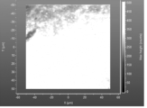
- the results are shown in Figures 1 and 2 and Tables 1 and 2.
- Example 3 Ge-doped nanodiamond particles were obtained in the same manner as in Example 1, except that 1 part by mass of tetraphenylgermane was used instead of 1 part by mass of triphenylsilanol and the oxidation treatment was performed at 520° C. for 2 hours. rice field.
- Comparative example 4 Ge-doped nanodiamond particles were obtained in the same manner as in Example 3, except that the oxidation treatment of Example 3 was performed at 470° C. for 2 hours.
Landscapes
- Chemical & Material Sciences (AREA)
- Engineering & Computer Science (AREA)
- Organic Chemistry (AREA)
- Inorganic Chemistry (AREA)
- Nanotechnology (AREA)
- Materials Engineering (AREA)
- Life Sciences & Earth Sciences (AREA)
- Geology (AREA)
- General Life Sciences & Earth Sciences (AREA)
- Crystallography & Structural Chemistry (AREA)
- Physics & Mathematics (AREA)
- General Physics & Mathematics (AREA)
- Condensed Matter Physics & Semiconductors (AREA)
- Manufacturing & Machinery (AREA)
- Composite Materials (AREA)
- Biophysics (AREA)
- Optics & Photonics (AREA)
- Carbon And Carbon Compounds (AREA)
Priority Applications (8)
| Application Number | Priority Date | Filing Date | Title |
|---|---|---|---|
| JP2023540374A JPWO2023013659A1 (https=) | 2021-08-04 | 2022-08-02 | |
| AU2022324914A AU2022324914A1 (en) | 2021-08-04 | 2022-08-02 | Heteroatom-doped nanodiamond particles and method for producing heteroatom-doped nanodiamond particles |
| CA3226911A CA3226911A1 (en) | 2021-08-04 | 2022-08-02 | Heteroatom-doped nanodiamond particles and method for producing heteroatom-doped nanodiamond particles |
| EP22853078.8A EP4382481A4 (en) | 2021-08-04 | 2022-08-02 | HETEROATOM-DOPED NANODIAMOND PARTICLES AND PROCESS FOR PRODUCING HETEROATOM-DOPED NANODIAMOND PARTICLES |
| IL310448A IL310448A (en) | 2021-08-04 | 2022-08-02 | Heteroatom-doped nanodiamond particles and method for producing heteroatom-doped nanodiamond particles |
| CN202280053501.9A CN117794856A (zh) | 2021-08-04 | 2022-08-02 | 杂原子掺杂纳米金刚石粒子以及杂原子掺杂纳米金刚石粒子的制造方法 |
| US18/580,434 US20250002355A1 (en) | 2021-08-04 | 2022-08-02 | Heteroatom-doped nanodiamond particles and method for producing heteroatom-doped nanodiamond particles |
| KR1020247003324A KR20240039127A (ko) | 2021-08-04 | 2022-08-02 | 이원자 도핑 나노다이아몬드 입자 및 이원자 도핑 나노다이아몬드 입자의 제조 방법 |
Applications Claiming Priority (4)
| Application Number | Priority Date | Filing Date | Title |
|---|---|---|---|
| JP2021127914 | 2021-08-04 | ||
| JP2021-127914 | 2021-08-04 | ||
| JP2022-043337 | 2022-03-18 | ||
| JP2022043337 | 2022-03-18 |
Publications (1)
| Publication Number | Publication Date |
|---|---|
| WO2023013659A1 true WO2023013659A1 (ja) | 2023-02-09 |
Family
ID=85155673
Family Applications (1)
| Application Number | Title | Priority Date | Filing Date |
|---|---|---|---|
| PCT/JP2022/029721 Ceased WO2023013659A1 (ja) | 2021-08-04 | 2022-08-02 | 異原子ドープナノダイヤモンド粒子及び異原子ドープナノダイヤモンド粒子の製造方法 |
Country Status (8)
| Country | Link |
|---|---|
| US (1) | US20250002355A1 (https=) |
| EP (1) | EP4382481A4 (https=) |
| JP (1) | JPWO2023013659A1 (https=) |
| KR (1) | KR20240039127A (https=) |
| AU (1) | AU2022324914A1 (https=) |
| CA (1) | CA3226911A1 (https=) |
| IL (1) | IL310448A (https=) |
| WO (1) | WO2023013659A1 (https=) |
Cited By (2)
| Publication number | Priority date | Publication date | Assignee | Title |
|---|---|---|---|---|
| IL300686A (en) * | 2023-02-15 | 2024-09-01 | Yeda Res & Dev | Fingerprinting using strain in particles |
| WO2024219059A1 (ja) * | 2023-04-17 | 2024-10-24 | 株式会社ダイセル | Nvセンターを有するナノダイヤモンド粒子及びその製造方法 |
Citations (4)
| Publication number | Priority date | Publication date | Assignee | Title |
|---|---|---|---|---|
| JP2016117852A (ja) * | 2014-12-22 | 2016-06-30 | 国立大学法人滋賀医科大学 | 蛍光ダイヤモンド及びその製造方法 |
| WO2020090825A1 (ja) * | 2018-10-31 | 2020-05-07 | 株式会社ダイセル | 蛍光ダイヤモンドおよびその製造方法 |
| WO2020195997A1 (ja) | 2019-03-26 | 2020-10-01 | 株式会社ダイセル | 異原子ドープナノダイヤモンド |
| WO2020195999A1 (ja) * | 2019-03-26 | 2020-10-01 | 株式会社ダイセル | 第14族元素がドープされたナノダイヤモンドの製造方法及び精製方法 |
Family Cites Families (1)
| Publication number | Priority date | Publication date | Assignee | Title |
|---|---|---|---|---|
| WO2020246500A1 (ja) * | 2019-06-05 | 2020-12-10 | 株式会社ダイセル | 表面修飾ナノダイヤモンド及び表面修飾ナノダイヤモンドの製造方法 |
-
2022
- 2022-08-02 EP EP22853078.8A patent/EP4382481A4/en active Pending
- 2022-08-02 AU AU2022324914A patent/AU2022324914A1/en active Pending
- 2022-08-02 KR KR1020247003324A patent/KR20240039127A/ko active Pending
- 2022-08-02 US US18/580,434 patent/US20250002355A1/en active Pending
- 2022-08-02 JP JP2023540374A patent/JPWO2023013659A1/ja active Pending
- 2022-08-02 CA CA3226911A patent/CA3226911A1/en active Pending
- 2022-08-02 WO PCT/JP2022/029721 patent/WO2023013659A1/ja not_active Ceased
- 2022-08-02 IL IL310448A patent/IL310448A/en unknown
Patent Citations (4)
| Publication number | Priority date | Publication date | Assignee | Title |
|---|---|---|---|---|
| JP2016117852A (ja) * | 2014-12-22 | 2016-06-30 | 国立大学法人滋賀医科大学 | 蛍光ダイヤモンド及びその製造方法 |
| WO2020090825A1 (ja) * | 2018-10-31 | 2020-05-07 | 株式会社ダイセル | 蛍光ダイヤモンドおよびその製造方法 |
| WO2020195997A1 (ja) | 2019-03-26 | 2020-10-01 | 株式会社ダイセル | 異原子ドープナノダイヤモンド |
| WO2020195999A1 (ja) * | 2019-03-26 | 2020-10-01 | 株式会社ダイセル | 第14族元素がドープされたナノダイヤモンドの製造方法及び精製方法 |
Non-Patent Citations (3)
| Title |
|---|
| EKIMOV E.A.; KONDRIN M.V.; KRIVOBOK V.S.; KHOMICH A.A.; VLASOV I.I.; KHMELNITSKIY R.A.; IWASAKI T.; HATANO M.: "Effect of Si, Ge and Sn dopant elements on structure and photoluminescence of nano- and microdiamonds synthesized from organic compounds", DIAMOND AND RELATED MATERIALS, ELSEVIER SCIENCE PUBLISHERS , AMSTERDAM, NL, vol. 93, 1 January 1900 (1900-01-01), NL , pages 75 - 83, XP085642095, ISSN: 0925-9635, DOI: 10.1016/j.diamond.2019.01.029 * |
| See also references of EP4382481A4 |
| VADYM N. MOCHALIN ET AL., NATURE NANOTECHNOLOGY, vol. 7, 2012, pages 11 - 23 |
Cited By (2)
| Publication number | Priority date | Publication date | Assignee | Title |
|---|---|---|---|---|
| IL300686A (en) * | 2023-02-15 | 2024-09-01 | Yeda Res & Dev | Fingerprinting using strain in particles |
| WO2024219059A1 (ja) * | 2023-04-17 | 2024-10-24 | 株式会社ダイセル | Nvセンターを有するナノダイヤモンド粒子及びその製造方法 |
Also Published As
| Publication number | Publication date |
|---|---|
| CA3226911A1 (en) | 2023-02-09 |
| KR20240039127A (ko) | 2024-03-26 |
| EP4382481A1 (en) | 2024-06-12 |
| US20250002355A1 (en) | 2025-01-02 |
| IL310448A (en) | 2024-03-01 |
| JPWO2023013659A1 (https=) | 2023-02-09 |
| AU2022324914A1 (en) | 2024-02-01 |
| EP4382481A4 (en) | 2025-12-10 |
Similar Documents
| Publication | Publication Date | Title |
|---|---|---|
| US12351463B2 (en) | Heteroatom-doped nanodiamond | |
| US12403437B2 (en) | Method for producing nanodiamonds doped with group 14 element, and method for purifying same | |
| JP2025013907A (ja) | 爆薬組成物及びその製造方法、並びに異原子ドープナノダイヤモンドの製造方法 | |
| WO2023013659A1 (ja) | 異原子ドープナノダイヤモンド粒子及び異原子ドープナノダイヤモンド粒子の製造方法 | |
| RU2817654C2 (ru) | Наноалмаз, допированный гетероатомом | |
| RU2825658C2 (ru) | Способ изготовления наноалмазов, допированных элементом группы 14, и способ их очистки | |
| RU2829756C2 (ru) | Взрывчатая композиция и способ ее изготовления и способ изготовления наноалмаза, допированного гетероатомом | |
| CN117794856A (zh) | 杂原子掺杂纳米金刚石粒子以及杂原子掺杂纳米金刚石粒子的制造方法 | |
| TWI915310B (zh) | 摻雜有雜原子之奈米鑽石 |
Legal Events
| Date | Code | Title | Description |
|---|---|---|---|
| 121 | Ep: the epo has been informed by wipo that ep was designated in this application |
Ref document number: 22853078 Country of ref document: EP Kind code of ref document: A1 |
|
| WWE | Wipo information: entry into national phase |
Ref document number: 2023540374 Country of ref document: JP |
|
| WWE | Wipo information: entry into national phase |
Ref document number: 2022324914 Country of ref document: AU Ref document number: AU2022324914 Country of ref document: AU |
|
| WWE | Wipo information: entry into national phase |
Ref document number: 18580434 Country of ref document: US |
|
| WWE | Wipo information: entry into national phase |
Ref document number: 3226911 Country of ref document: CA |
|
| WWE | Wipo information: entry into national phase |
Ref document number: 310448 Country of ref document: IL |
|
| ENP | Entry into the national phase |
Ref document number: 20247003324 Country of ref document: KR Kind code of ref document: A |
|
| WWE | Wipo information: entry into national phase |
Ref document number: 202280053501.9 Country of ref document: CN |
|
| ENP | Entry into the national phase |
Ref document number: 2022324914 Country of ref document: AU Date of ref document: 20220802 Kind code of ref document: A |
|
| WWE | Wipo information: entry into national phase |
Ref document number: 11202400122T Country of ref document: SG |
|
| WWE | Wipo information: entry into national phase |
Ref document number: 2024105292 Country of ref document: RU |
|
| NENP | Non-entry into the national phase |
Ref country code: DE |
|
| ENP | Entry into the national phase |
Ref document number: 2022853078 Country of ref document: EP Effective date: 20240304 |