WO2023013199A1 - 高周波回路及び通信装置 - Google Patents
高周波回路及び通信装置 Download PDFInfo
- Publication number
- WO2023013199A1 WO2023013199A1 PCT/JP2022/019911 JP2022019911W WO2023013199A1 WO 2023013199 A1 WO2023013199 A1 WO 2023013199A1 JP 2022019911 W JP2022019911 W JP 2022019911W WO 2023013199 A1 WO2023013199 A1 WO 2023013199A1
- Authority
- WO
- WIPO (PCT)
- Prior art keywords
- terminal
- switch
- circuit
- frequency circuit
- reception
- Prior art date
- Legal status (The legal status is an assumption and is not a legal conclusion. Google has not performed a legal analysis and makes no representation as to the accuracy of the status listed.)
- Ceased
Links
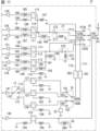
Images





Classifications
-
- H—ELECTRICITY
- H04—ELECTRIC COMMUNICATION TECHNIQUE
- H04B—TRANSMISSION
- H04B1/00—Details of transmission systems, not covered by a single one of groups H04B3/00 - H04B13/00; Details of transmission systems not characterised by the medium used for transmission
- H04B1/005—Details of transmission systems, not covered by a single one of groups H04B3/00 - H04B13/00; Details of transmission systems not characterised by the medium used for transmission adapting radio receivers, transmitters andtransceivers for operation on two or more bands, i.e. frequency ranges
- H04B1/0067—Details of transmission systems, not covered by a single one of groups H04B3/00 - H04B13/00; Details of transmission systems not characterised by the medium used for transmission adapting radio receivers, transmitters andtransceivers for operation on two or more bands, i.e. frequency ranges with one or more circuit blocks in common for different bands
- H04B1/0075—Details of transmission systems, not covered by a single one of groups H04B3/00 - H04B13/00; Details of transmission systems not characterised by the medium used for transmission adapting radio receivers, transmitters andtransceivers for operation on two or more bands, i.e. frequency ranges with one or more circuit blocks in common for different bands using different intermediate frequencied for the different bands
- H04B1/0078—Details of transmission systems, not covered by a single one of groups H04B3/00 - H04B13/00; Details of transmission systems not characterised by the medium used for transmission adapting radio receivers, transmitters andtransceivers for operation on two or more bands, i.e. frequency ranges with one or more circuit blocks in common for different bands using different intermediate frequencied for the different bands with a common intermediate frequency amplifier for the different intermediate frequencies, e.g. when using switched intermediate frequency filters
-
- H—ELECTRICITY
- H03—ELECTRONIC CIRCUITRY
- H03H—IMPEDANCE NETWORKS, e.g. RESONANT CIRCUITS; RESONATORS
- H03H7/00—Multiple-port networks comprising only passive electrical elements as network components
- H03H7/38—Impedance-matching networks
-
- H—ELECTRICITY
- H04—ELECTRIC COMMUNICATION TECHNIQUE
- H04B—TRANSMISSION
- H04B1/00—Details of transmission systems, not covered by a single one of groups H04B3/00 - H04B13/00; Details of transmission systems not characterised by the medium used for transmission
-
- H—ELECTRICITY
- H04—ELECTRIC COMMUNICATION TECHNIQUE
- H04B—TRANSMISSION
- H04B1/00—Details of transmission systems, not covered by a single one of groups H04B3/00 - H04B13/00; Details of transmission systems not characterised by the medium used for transmission
- H04B1/005—Details of transmission systems, not covered by a single one of groups H04B3/00 - H04B13/00; Details of transmission systems not characterised by the medium used for transmission adapting radio receivers, transmitters andtransceivers for operation on two or more bands, i.e. frequency ranges
- H04B1/0053—Details of transmission systems, not covered by a single one of groups H04B3/00 - H04B13/00; Details of transmission systems not characterised by the medium used for transmission adapting radio receivers, transmitters andtransceivers for operation on two or more bands, i.e. frequency ranges with common antenna for more than one band
- H04B1/006—Details of transmission systems, not covered by a single one of groups H04B3/00 - H04B13/00; Details of transmission systems not characterised by the medium used for transmission adapting radio receivers, transmitters andtransceivers for operation on two or more bands, i.e. frequency ranges with common antenna for more than one band using switches for selecting the desired band
-
- H—ELECTRICITY
- H04—ELECTRIC COMMUNICATION TECHNIQUE
- H04B—TRANSMISSION
- H04B1/00—Details of transmission systems, not covered by a single one of groups H04B3/00 - H04B13/00; Details of transmission systems not characterised by the medium used for transmission
- H04B1/02—Transmitters
- H04B1/04—Circuits
-
- H—ELECTRICITY
- H04—ELECTRIC COMMUNICATION TECHNIQUE
- H04B—TRANSMISSION
- H04B1/00—Details of transmission systems, not covered by a single one of groups H04B3/00 - H04B13/00; Details of transmission systems not characterised by the medium used for transmission
- H04B1/06—Receivers
- H04B1/16—Circuits
- H04B1/18—Input circuits, e.g. for coupling to an antenna or a transmission line
-
- H—ELECTRICITY
- H04—ELECTRIC COMMUNICATION TECHNIQUE
- H04B—TRANSMISSION
- H04B1/00—Details of transmission systems, not covered by a single one of groups H04B3/00 - H04B13/00; Details of transmission systems not characterised by the medium used for transmission
- H04B1/38—Transceivers, i.e. devices in which transmitter and receiver form a structural unit and in which at least one part is used for functions of transmitting and receiving
- H04B1/40—Circuits
Definitions
- the present invention generally relates to high frequency circuits and communication devices, and more particularly to high frequency circuits with multiple filters and communication devices with high frequency circuits.
- Patent Document 1 describes a multiplexer that includes a switch and a duplexer.
- the switch has a common terminal and a select terminal.
- a duplexer includes a transmit filter and a receive filter.
- An antenna terminal is connected to the common terminal of the switch, and a duplexer (transmission filter, reception filter) is connected to the selection terminal of the switch.
- the first filter (receiving filter) and the second filter (transmitting filter) are bundled into one, and reception sensitivity may deteriorate due to bundling loss.
- An object of the present invention is to provide a high-frequency circuit and a communication device capable of reducing reception sensitivity deterioration due to bundling loss.
- a high-frequency circuit includes an antenna terminal, a transmission filter, a plurality of reception filters, a first switch, and a second switch.
- the first switch has a first terminal, a second terminal and a third terminal.
- the second switch has a fourth terminal and a fifth terminal. In the first switch, the first terminal can be connected to the second terminal or the third terminal. In the second switch, the fourth terminal is connectable to the fifth terminal.
- Each of the plurality of receive filters is connected to the second terminal or the third terminal of the first switch.
- the first terminal of the first switch is connected to the antenna terminal.
- the fourth terminal of the second switch is connected to the second terminal of the first switch.
- the fifth terminal of the second switch is connected to the transmit filter.
- a communication device includes the high-frequency circuit and a signal processing circuit.
- the signal processing circuit is connected to the high frequency circuit.
- the high-frequency circuit and the communication device it is possible to reduce deterioration of reception sensitivity due to bundling loss.
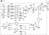
- FIG. 1 is a schematic diagram of a high-frequency circuit according to Embodiment 1.
- FIG. FIG. 2 is a schematic diagram of a communication device according to the first embodiment.
- 3A and 3B are circuit diagrams showing specific examples of matching circuits used in the high frequency circuit of the same.
- FIG. 4 is a schematic diagram of a high frequency circuit according to the second embodiment.
- 5A and 5B are circuit diagrams showing specific examples of matching circuits used in the high frequency circuit of the same.
- FIG. 6 is a schematic diagram of a high frequency circuit according to a modification of the second embodiment.
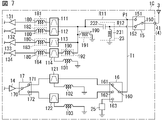
- FIG. 7 is a schematic diagram of a high frequency circuit according to the third embodiment.
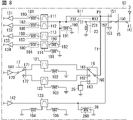
- FIG. 8 is a schematic diagram of a high frequency circuit according to the fourth embodiment.
- FIG. 9 is a schematic diagram of a high frequency circuit according to the fifth embodiment.
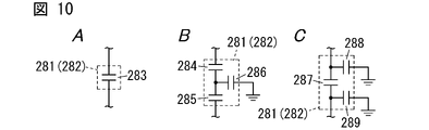
- 10A to 10C are circuit diagrams showing specific examples of phase circuits used in the high frequency circuit of the same.
- FIG. 11 is a schematic diagram of a high frequency circuit according to the sixth embodiment.
- Embodiment 1 (1) High Frequency Circuit First, the configuration of a high frequency circuit 1 according to Embodiment 1 will be described with reference to the drawings.
- the high-frequency circuit 1 is used, for example, in a communication device 10, as shown in FIG.
- the communication device 10 is, for example, a mobile phone such as a smart phone.
- the communication device 10 is not limited to a mobile phone, and may be, for example, a wearable terminal such as a smartwatch.
- the high-frequency circuit 1 is, for example, a circuit capable of complying with the 4G (fourth generation mobile communication) standard, the 5G (fifth generation mobile communication) standard, and the like.
- the 4G standard is, for example, the 3GPP (registered trademark, Third Generation Partnership Project) LTE (registered trademark, Long Term Evolution) standard.
- the 5G standard is, for example, 5G NR (New Radio).
- the high-frequency circuit 1 is, for example, a circuit capable of supporting carrier aggregation and dual connectivity.
- carrier aggregation and dual connectivity refer to technologies used for communication that simultaneously use radio waves of multiple frequency bands.
- communication of signals by carrier aggregation or dual connectivity is also referred to as simultaneous communication.
- simultaneous communication means that transmission and reception of signals by carrier aggregation or dual connectivity are possible.
- the communication device 10 performs communication in a plurality of communication bands. More specifically, the communication device 10 transmits transmission signals for each of the plurality of communication bands and receives reception signals for each of the plurality of communication bands. Specifically, the high-frequency circuit 1 receives a received signal in the first communication band, a received signal in the second communication band, a received signal in the third communication band, and a received signal in the fourth communication band. The high-frequency circuit 1 also transmits a transmission signal in the first communication band, a transmission signal in the second communication band, and a transmission signal in the fifth communication band.
- the transmission signals and reception signals of multiple communication bands are, for example, FDD (Frequency Division Duplex) signals.
- the transmission signals and reception signals of a plurality of communication bands are not limited to FDD signals, and may be, for example, TDD (Time Division Duplex) signals.
- FDD is a wireless communication technology that allocates different frequency bands for transmission and reception in wireless communication and performs transmission and reception.
- TDD is a wireless communication technology that allocates the same frequency band to transmission and reception in wireless communication and switches between transmission and reception every time.
- the high-frequency circuit 1 according to the first embodiment includes (four in the illustrated example) low-noise amplifiers 131 to 134 and a power amplifier 14 . Moreover, the high-frequency circuit 1 according to the first embodiment further includes a first switch 15 , a second switch 16 and a third switch 17 . Further, the high-frequency circuit 1 according to the first embodiment includes a plurality of (four in the illustrated example) input matching circuits 181 to 184 and a plurality of (four in the illustrated example) matching circuits 23, 24, 191, and 192. Prepare more. Moreover, the high-frequency circuit 1 according to the first embodiment further includes an external connection terminal 4 .
- the plurality of receive filters 111 to 114 are filters that pass received signals of communication bands different from each other. More specifically, the reception filter 111 is a filter that allows the reception signal of the third communication band to pass.
- the reception filter 112 is a filter that allows the reception signal of the first communication band to pass.
- the reception filter 113 is a filter that allows the reception signal of the second communication band to pass.
- the reception filter 114 is a filter that passes the reception signal of the fourth communication band.
- the reception filter 111 and the reception filter 112 are integrated into one chip. "The receiving filter 111 and the receiving filter 112 are integrated into one chip" means that the circuit that configures the receiving filter 111 and the circuit that configures the receiving filter 112 are formed on a common (single) substrate. Say things.
- the first communication band is, for example, Band 1 of the 3GPP LTE standard, and the reception band of the first communication band is 2110 MHz-2170 MHz.
- the second communication band is, for example, Band 3 of the 3GPP LTE standard, and the reception band of the second communication band is 1805 MHz-1880 MHz.
- the third communication band is, for example, Band 40 of the 3GPP LTE standard, and the reception band of the third communication band is 2300 MHz-2400 MHz.
- the fourth communication band is, for example, Band 32 of the 3GPP LTE standard, and the reception band of the fourth communication band is 1452 MHz-1496 MHz.
- the reception filter 111 is provided between a low-noise amplifier 131 and the first switch 15, which will be described later.
- the reception filter 112 is provided between a low-noise amplifier 132 and the first switch 15, which will be described later.
- the reception filter 113 is provided between a low noise amplifier 133 and the first switch 15, which will be described later.
- the reception filter 114 is provided between a low-noise amplifier 134 and the first switch 15, which will be described later.
- Each of the reception filters 111 to 114 passes a reception signal in the reception band of the corresponding communication band among the high frequency signals input from the antenna terminal 41, which will be described later.
- the inductor 101 is connected between the parallel arm resonators forming the reception filter 114 and the ground. Thereby, the attenuation pole of the reception filter 114 is adjusted.
- the plurality of transmission filters 121 and 122 are filters that pass transmission signals of communication bands different from each other. More specifically, the transmission filter 121 is a filter that passes the transmission signal of the second communication band and the transmission signal of the fifth communication band. The transmission filter 122 is a filter that passes the transmission signal of the first communication band.
- the first communication band is Band 1 of the 3GPP LTE standard, and the transmission band of the first communication band is 1920 MHz-1980 MHz.
- the second communication band is Band 3 of the 3GPP LTE standard, and the transmission band of the second communication band is 1710 MHz-1785 MHz.
- the fifth communication band is, for example, Band 66 of the 3GPP LTE standard, and the transmission band of the fifth communication band is 1710 MHz-1780 MHz.
- the transmission band of the fifth communication band is included in the transmission band of the second communication band.
- Each of the multiple transmission filters 121 and 122 is provided between the power amplifier 14 and the second switch 16 .
- Each of the plurality of transmission filters 121 and 122 passes a transmission signal in the transmission band of the corresponding communication band among the high frequency signals amplified by the power amplifier 14 .
- the inductor 102 is connected between the parallel arm resonators forming the transmission filter 121 and the ground.
- an inductor 103 is connected between the parallel arm resonator forming the transmission filter 122 and the ground.
- Each of the plurality of low-noise amplifiers 131 to 134 is an amplifier that amplifies a received signal with low noise.
- the low noise amplifier 131 is provided between the first signal output terminal (not shown) and the reception filter 111 .
- the low noise amplifier 132 is provided between the second signal output terminal (not shown) and the reception filter 112 .
- Low noise amplifier 133 is provided between a third signal output terminal (not shown) and reception filter 113 .
- Low noise amplifier 134 is provided between a fourth signal output terminal (not shown) and reception filter 114 .
- Each of the first to fourth signal output terminals is a terminal for outputting a received signal from the high frequency circuit 1 to an external circuit (for example, the signal processing circuit 2).
- Each of the plurality of low noise amplifiers 131-134 has an input terminal (not shown) and an output terminal (not shown).
- An input terminal of the low noise amplifier 131 is connected to an input matching circuit 181 which will be described later.
- An output terminal of the low-noise amplifier 131 is connected to an external circuit (for example, the signal processing circuit 2) via a first signal output terminal.
- An input terminal of the low noise amplifier 132 is connected to an input matching circuit 182 which will be described later.
- An output terminal of the low-noise amplifier 132 is connected to an external circuit (for example, the signal processing circuit 2) via a second signal output terminal.
- An input terminal of the low noise amplifier 133 is connected to an input matching circuit 183 which will be described later.
- An output terminal of the low noise amplifier 133 is connected to an external circuit (for example, the signal processing circuit 2) via a third signal output terminal.
- An input terminal of the low noise amplifier 134 is connected to an input matching circuit 184 which will be described later.
- An output terminal of the low-noise amplifier 134 is connected to an external circuit (for example, the signal processing circuit 2) via a fourth signal output terminal.
- the power amplifier 14 is an amplifier that amplifies a transmission signal.
- the power amplifier 14 is provided between a signal input terminal (not shown) and the multiple transmission filters 121 and 122 .
- a signal input terminal is a terminal for inputting a transmission signal from an external circuit (for example, the signal processing circuit 2 ) to the high frequency circuit 1 .
- the power amplifier 14 has an input terminal (not shown) and an output terminal (not shown).
- An input terminal of the power amplifier 14 is connected to an external circuit (for example, the signal processing circuit 2) via a signal input terminal.
- the output terminal of the power amplifier 14 is connected to the common terminal 170 of the third switch 17 and can be connected to a plurality of transmission filters 121 and 122 via the third switch 17 .
- the power amplifier 14 is controlled by, for example, a controller (not shown).
- Input matching circuit 181 is provided between low noise amplifier 131 and reception filter 111 .
- the input matching circuit 181 is a circuit for impedance matching between the low noise amplifier 131 and the reception filter 111 .
- the input matching circuit 181 includes an inductor 180.
- the inductor 180 of the input matching circuit 181 is provided on the input side of the low noise amplifier 131 .
- the input matching circuit 181 is not limited to a configuration including one inductor 180.
- the input matching circuit 181 may include a plurality of inductors, or may include a plurality of inductors and a plurality of capacitors. may
- the input matching circuit 182 is provided between the low noise amplifier 132 and the reception filter 112 .
- the input matching circuit 182 is a circuit for impedance matching between the low noise amplifier 132 and the reception filter 112 .
- the input matching circuit 182 includes an inductor 180.
- the inductor 180 of the input matching circuit 182 is provided on the input side of the low noise amplifier 132 .
- the input matching circuit 182 is not limited to a configuration including one inductor 180.
- the input matching circuit 182 may include a plurality of inductors, or may include a plurality of inductors and a plurality of capacitors. may
- the input matching circuit 183 is provided between the low noise amplifier 133 and the reception filter 113 .
- the input matching circuit 183 is a circuit for impedance matching between the low noise amplifier 133 and the reception filter 113 .
- the input matching circuit 183 includes an inductor 180.
- the inductor 180 of the input matching circuit 183 is provided on the input side of the low noise amplifier 133 .
- the input matching circuit 183 is not limited to a configuration including one inductor 180.
- the input matching circuit 183 may include a plurality of inductors, or may include a plurality of inductors and a plurality of capacitors. may
- the input matching circuit 184 is provided between the low noise amplifier 134 and the reception filter 114 .
- the input matching circuit 184 is a circuit for impedance matching between the low noise amplifier 134 and the reception filter 114 .
- the input matching circuit 184 includes an inductor 180.
- the inductor 180 of the input matching circuit 184 is provided on the input side of the low noise amplifier 134 .
- the input matching circuit 184 is not limited to a configuration including one inductor 180.
- the input matching circuit 184 may include a plurality of inductors, or may include a plurality of inductors and a plurality of capacitors. may
- the matching circuit 191 is provided between the plurality of reception filters 111 to 114 and the first switch 15 .
- the matching circuit 191 is a circuit for impedance matching between the plurality of reception filters 111 to 114 and the first switch 15 .
- a matching circuit 191 includes an inductor 190 .
- the inductor 190 of the matching circuit 191 is provided between the input terminals (not shown) of the plurality of reception filters 111 to 114 and the ground.
- the matching circuit 191 is not limited to a configuration including one inductor 190.
- the matching circuit 191 may include a plurality of inductors, or may include a plurality of inductors and a plurality of capacitors. good too.
- a matching circuit 192 is provided between the reception filter 114 and the first switch 15 .
- the matching circuit 192 is a circuit for impedance matching between the reception filter 114 and the first switch 15 .
- the matching circuit 192 includes an inductor 190.
- Inductor 190 of matching circuit 192 is provided between an input terminal (not shown) of reception filter 114 and matching circuit 23 .
- the matching circuit 192 is not limited to a configuration including one inductor 190.
- the matching circuit 192 may include a plurality of inductors, or may include a plurality of inductors and a plurality of capacitors. good too.
- a matching circuit 23 is provided between the plurality of reception filters 111 to 114 and the first switch 15 .
- the matching circuit 23 is a circuit for achieving impedance matching between the plurality of reception filters 111 to 114 and the first switch 15 .
- the matching circuit 23 includes an inductor 231 and a capacitor 232.
- the inductor 231 of the matching circuit 23 is provided between the signal path R1 and the ground.
- the capacitor 232 of the matching circuit 23 is provided between the input terminals (not shown) of the reception filters 111 to 114 and the selection terminal 151 of the first switch 15 .
- a signal path R1 is a signal path that connects input terminals of the plurality of reception filters 111 to 114 and the selection terminal 151 of the first switch 15 .
- the matching circuit 24 is provided between the selection terminal 151 of the first switch 15 and the common terminal 160 of the second switch 16, as shown in FIG.
- the matching circuit 24 is a circuit for greatly increasing the impedance of the signal path T1 in the frequency band of the reception band of the reception signal received through the antenna 3 .
- the signal path T1 becomes open when viewed from the connection point P1 on the signal path R1 in the frequency band of the reception band of the received signal.
- a signal path T1 is a signal path branched from a connection point P1 on the signal path R1 and a signal path connecting the connection point P1 and the common terminal 160 of the second switch 16 .
- the matching circuit 24 includes an inductor 241, as shown in FIG. 3A.
- the inductor 241 of the matching circuit 24 is provided between the connection point P1 on the signal path R1 and the common terminal 160 of the second switch 16 .
- the first switch 15 switches the filter connected to the antenna terminal 41 among a plurality of filters including the plurality of reception filters 111 to 114 and the plurality of transmission filters 121 and 122 . That is, the first switch 15 is a switch for switching the path to be connected to the antenna terminal 41 .
- the first switch 15 has a common terminal 150 and a plurality of (two in the illustrated example) selection terminals 151 and 152 . Common terminal 150 is connected to antenna terminal 41 .
- the selection terminal 151 is connected to a plurality of reception filters 111-114. Also, the selection terminal 151 is connected to a plurality of transmission filters 121 and 122 via a second switch 16 which will be described later.
- the selection terminal 152 is connected to the filters other than the plurality of reception filters 111 to 114 and the plurality of transmission filters 121 and 122 among the plurality of filters.
- the common terminal 150 is the first terminal
- the selection terminals 151 are the second and third terminals. That is, the first switch 15 has a first terminal (common terminal 150), a second terminal and a third terminal (selection terminal 151). In the first switch 15, the first terminal can be connected to at least one of the second terminal and the third terminal. Also, in the first switch 15, the third terminal is also used as the second terminal.
- the first switch 15 switches the connection state between the common terminal 150 and the plurality of selection terminals 151 and 152 .
- the first switch 15 is controlled by, for example, the signal processing circuit 2 (see FIG. 2).
- the first switch 15 electrically connects the common terminal 150 and at least one of the plurality of selection terminals 151 and 152 according to the control signal from the RF signal processing circuit 21 (see FIG. 2) of the signal processing circuit 2 .
- the second switch 16 switches the transmission filter connected to the antenna terminal 41 among the plurality of transmission filters 121 and 122 . That is, the second switch 16 is a switch for switching the path to be connected to the antenna terminal 41 .
- the second switch 16 has a common terminal 160 and a plurality of (two in the illustrated example) selection terminals 161 and 162 .
- the common terminal 160 is connected to the selection terminal 151 of the first switch 15 . More specifically, common terminal 160 is connected to signal path R1 at connection point P1 on signal path R1.
- the plurality of reception filters 111 to 114 and the plurality of transmission filters 121 and 122 are bundled into one at the selection terminal 151 of the first switch 15 .
- each of the plurality of reception filters 111 to 114 is connected to the selection terminal 151 (second terminal) of the first switch 15, and the common terminal 160 (fourth terminal) of the second switch 16 is connected to the first switch 15 selection terminals 151 , and the selection terminal 161 (fifth terminal) of the second switch 16 is connected to the transmission filter 121 .
- the common terminal 160 can be connected to the selection terminal 161 in the second switch 16 .
- the selection terminal 161 is connected to the transmission filter 121 .
- Selection terminal 162 is connected to transmission filter 122 .
- the common terminal 160 is the fourth terminal and the selection terminal 161 is the fifth terminal. That is, the second switch 16 has a fourth terminal (common terminal 160) and a fifth terminal (selection terminal 161). The fourth terminal of the second switch 16 can be connected to the fifth terminal.
- the transmission filter 121 is a transmission filter connected to the fifth terminal of the second switch 16 .
- the second switch 16 switches the connection state between the common terminal 160 and the plurality of selection terminals 161 and 162 .
- the second switch 16 is controlled by, for example, the signal processing circuit 2 (see FIG. 2).
- the second switch 16 electrically connects the common terminal 160 and at least one of the plurality of selection terminals 161 and 162 according to the control signal from the RF signal processing circuit 21 (see FIG. 2) of the signal processing circuit 2 .
- the third switch 17 switches the transmission filter connected to the power amplifier 14 among the multiple transmission filters 121 and 122 . That is, the third switch 17 is a switch for switching the path to be connected to the power amplifier 14 .
- the third switch 17 has a common terminal 170 and a plurality of (two in the illustrated example) selection terminals 171 and 172 .
- the common terminal 170 is connected to the output terminal of the power amplifier 14 .
- the selection terminal 171 is connected to the transmission filter 121 .
- the selection terminal 172 is connected to the transmission filter 122 .
- the third switch 17 switches the connection state between the common terminal 170 and the plurality of selection terminals 171 and 172 .
- the third switch 17 is controlled by, for example, the signal processing circuit 2 (see FIG. 2).
- the third switch 17 electrically connects the common terminal 170 and at least one of the plurality of selection terminals 171 and 172 according to the control signal from the RF signal processing circuit 21 (see FIG. 2) of the signal processing circuit 2 .
- the plurality of external connection terminals 4 are terminals for electrically connecting to an external circuit (for example, the signal processing circuit 2).
- the plurality of external connection terminals 4 includes an antenna terminal 41, a signal input terminal (not shown), first to fourth signal output terminals (not shown), a plurality of control terminals (not shown), a plurality of a ground terminal (not shown) of the .
- An antenna 3 is connected to the antenna terminal 41 .
- the antenna terminal 41 is connected to the first switch 15 .
- the antenna terminal 41 is connected to a plurality of reception filters 111 to 114 via the first switch 15 .
- the antenna terminal 41 is connected to multiple transmission filters 121 and 122 via the first switch 15 and the second switch 16 .
- a signal input terminal is a terminal for inputting a transmission signal from an external circuit (for example, the signal processing circuit 2 ) to the high frequency circuit 1 .
- a signal input terminal is connected to a power amplifier 14 in the high frequency circuit 1 .
- the first to fourth signal output terminals are terminals for outputting the received signal from the high frequency circuit 1 to an external circuit (for example, the signal processing circuit 2).
- the first signal output terminal is connected to the low noise amplifier 131
- the second signal output terminal is connected to the low noise amplifier 132
- the third signal output terminal is connected to the low noise amplifier 133
- the fourth signal output terminal is connected. is connected to the low noise amplifier 134 .
- a plurality of control terminals are terminals for inputting control signals from an external circuit (for example, the signal processing circuit 2 ) to the high frequency circuit 1 .
- an external circuit for example, the signal processing circuit 2
- a plurality of control terminals are connected to a controller (not shown).
- the plurality of ground terminals are terminals that are electrically connected to a ground electrode of an external substrate (not shown) included in the communication device 10 and are supplied with a ground potential.
- a plurality of ground terminals are connected to a ground layer (not shown) of a mounting board (not shown), which will be described later.
- the high-frequency circuit 1 includes a mounting board (not shown) and a plurality of electronic components (not shown).
- the high-frequency circuit 1 includes, as a plurality of electronic components, a plurality of reception filters 111 to 114, a plurality of transmission filters 121 and 122, a plurality of low noise amplifiers 131 to 134, a power amplifier 14, a first switch 15, and a second A second switch 16 and a third switch 17 are provided.
- the high-frequency circuit 1 further includes a plurality of input matching circuits 181 to 184 and a plurality of matching circuits 23, 24, 191, 192 as the plurality of electronic components.
- the high-frequency circuit 1 further includes a plurality of inductors 101 to 103 as a plurality of electronic components.
- the high frequency circuit 1 can be electrically connected to an external substrate (not shown).
- the external board corresponds to, for example, the mother board of the communication device 10 such as a mobile phone and communication equipment.
- the high-frequency circuit 1 can be electrically connected to the external substrate not only when the high-frequency circuit 1 is directly mounted on the external substrate, but also when the high-frequency circuit 1 is indirectly mounted on the external substrate. including cases where Further, the case where the high-frequency circuit 1 is indirectly mounted on the external substrate is, for example, the case where the high-frequency circuit 1 is mounted on another high-frequency circuit mounted on the external substrate.
- the mounting substrate has a first principal surface and a second principal surface.
- the first main surface and the second main surface face each other in the thickness direction of the mounting substrate.
- the second main surface faces the mounting substrate side main surface of the external substrate when the high-frequency circuit 1 is provided on the external substrate.
- the mounting board is, for example, a single-sided mounting board having a plurality of electronic components mounted on the first main surface. Note that the mounting board is not limited to a single-sided mounting board, and may be a double-sided mounting board in which a plurality of electronic components are mounted on the first main surface and the second main surface.
- the mounting board is a multi-layer board in which multiple dielectric layers are laminated.
- the mounting board has a plurality of conductive layers and a plurality of via conductors (including through electrodes).
- the plurality of conductive layers includes a ground layer at ground potential.
- a plurality of via conductors are used for electrical connection between the elements (including the electronic components described above) mounted on the first main surface of the mounting board and the conductive layers of the mounting board.
- a plurality of via conductors are used for electrical connection between the conductive layer of the mounting substrate and the external connection terminals 4 .
- a plurality of electronic components are arranged on the first main surface of the mounting substrate.
- a plurality of external connection terminals 4 are arranged on the second main surface of the mounting substrate.
- a plurality of electronic components are arranged on the first main surface of the mounting substrate. More specifically, a plurality of electronic components are mounted on the first main surface of the mounting board. In addition, in each of the plurality of electronic components, part of the electronic component may be mounted on the first main surface of the mounting substrate, and the remainder of the electronic component may be mounted inside the mounting substrate. In short, each of the plurality of electronic components has at least a portion that is arranged closer to the first main surface than the second main surface on the mounting substrate and that is mounted on the first main surface.
- the plurality of external connection terminals 4 are terminals for electrically connecting a mounting substrate (not shown) and an external substrate (not shown).
- a plurality of external connection terminals 4 are arranged on the second main surface of the mounting substrate.
- the plurality of external connection terminals 4 are columnar (for example, columnar) electrodes provided on the second main surface of the mounting substrate.
- the material of the plurality of external connection terminals 4 is, for example, metal (eg, copper, copper alloy, etc.).
- the communication device 10 includes a high frequency circuit 1, a signal processing circuit 2, and an antenna 3, as shown in FIG.
- the communication device 10 further includes an external substrate (not shown) on which the high frequency circuit 1 is mounted.
- the external board is, for example, a printed wiring board.
- the external substrate has a ground electrode to which a ground potential is applied.
- the antenna 3 is connected to the antenna terminal 41 of the high frequency circuit 1, as shown in FIGS.
- the antenna 3 has a transmission function of radiating a transmission signal output from the high-frequency circuit 1 as radio waves, and a reception function of receiving a reception signal as radio waves from the outside and outputting the radio waves to the high-frequency circuit 1 .
- the signal processing circuit 2 includes an RF signal processing circuit 21 and a baseband signal processing circuit 22, as shown in FIG.
- the signal processing circuit 2 processes signals passing through the high frequency circuit 1 . More specifically, the signal processing circuit 2 processes transmission signals and reception signals.
- the RF signal processing circuit 21 is, for example, an RFIC (Radio Frequency Integrated Circuit).
- the RF signal processing circuit 21 performs signal processing on high frequency signals.
- the RF signal processing circuit 21 performs signal processing such as up-conversion on the transmission signal output from the baseband signal processing circuit 22 and outputs the signal-processed transmission signal to the high frequency circuit 1 .
- the RF signal processing circuit 21 also performs signal processing such as down-conversion on the received signal output from the high frequency circuit 1 and outputs the processed received signal to the baseband signal processing circuit 22 .
- the baseband signal processing circuit 22 is, for example, a BBIC (Baseband Integrated Circuit).
- the baseband signal processing circuit 22 performs predetermined signal processing on a transmission signal from outside the signal processing circuit 2 .
- the received signal processed by the baseband signal processing circuit 22 is used, for example, as an image signal for image display or as an audio signal for calling.
- the RF signal processing circuit 21 controls connection of each of the first switch 15, the second switch 16 and the third switch 17 included in the high frequency circuit 1 based on the transmission and reception of high frequency signals (transmission signal, reception signal). It also has a function as a control unit. Specifically, the RF signal processing circuit 21 switches connection of each of the first switch 15, the second switch 16 and the third switch 17 of the high frequency circuit 1 by a control signal (not shown). Note that the control unit may be provided outside the RF signal processing circuit 21 , for example, in the high frequency circuit 1 or the baseband signal processing circuit 22 .
- the matching circuit 24 is provided between the connection point P1 on the signal path R1 and the common terminal 160 of the second switch 16.
- the connection point P1 the reception band of the impedance on the transmission circuit side including the signal path T1 can be brought into a nearly open state (that is, a very large impedance state).
- the reception signal is less likely to leak to the signal path T1 side, so that deterioration of reception sensitivity due to bundling loss can be reduced.
- the term “bundling loss” refers to the loss of received signals that occurs when the transmission filter and the reception filter are bundled.
- the "bundling loss” refers to the loss of the received signal that occurs when the transmission filter is bundled with the reception filter.
- the common terminal 150 (first terminal) of the first switch 15 can be connected to the selection terminal 151 (second terminal), and the common terminal 150 (second terminal) of the second switch 16 can A terminal 160 (fourth terminal) is connectable to a selection terminal 161 (fifth terminal).
- each of the plurality of reception filters 111 to 114 is connected to the selection terminal 151 of the first switch 15 and the common terminal 150 of the first switch 15 is connected to the antenna terminal 41 .
- the common terminal 160 of the second switch 16 is connected to the selection terminal 151 of the first switch 15 and the selection terminal 161 of the second switch 16 is connected to the transmission filter 121 . This makes it possible to reduce deterioration of reception sensitivity due to bundling loss.
- the high-frequency circuit 1 includes a matching circuit 24 connected between the selection terminal 151 of the first switch 15 and the common terminal 160 of the second switch 16 .
- the connection point P1 the reception band of the impedance on the transmission circuit side including the signal path T1 can be brought into a nearly open state (that is, a very large impedance state).
- the reception signal is less likely to leak to the signal path T1 side, so that deterioration of reception sensitivity due to bundling loss can be reduced.
- all of the plurality of reception filters 111 to 114 are connected to (the selection terminal 151 of) the first switch 15 in the front stage, and the reception filter is connected to the second switch 16 in the rear stage. Not connected.
- a plurality of transmission filters 121 and 122 are connected to (the selection terminals 161 and 162 of) the second switch 16 in the latter stage. This makes it possible to reduce deterioration in reception sensitivity due to bundling loss for all of the plurality of reception filters 111 to 114 .
- the high-frequency circuit 1 as shown in FIG. This makes it possible to reduce the off-capacitance of the first switch 15 compared to the case where each of the plurality of transmission filters 121 and 122 is directly connected to the first switch 15. As a result, the first switch 15 It is possible to reduce the bundling loss in In addition, intermodulation distortion (IMD) between the plurality of transmission filters 121 and 122 can be reduced compared to the case where each of the plurality of transmission filters 121 and 122 is directly connected to the first switch 15. It becomes possible.
- IMD intermodulation distortion
- the matching circuit 24 is provided between the selection terminal 151 of the first switch 15 and the common terminal 160 of the second switch 16 in the first embodiment, the matching circuit 24 may be omitted.
- the reception band of the impedance on the transmission circuit side including the signal path T1 is opened at the connection point P1. It is possible to make the state close to each other (that is, the state in which the impedance is very large). As a result, the reception signal is less likely to leak to the signal path T1 side, so that deterioration of reception sensitivity due to bundling loss can be reduced.
- the matching circuit 24 includes the inductor 241 as shown in FIG. 3A in the first embodiment, the matching circuit 24 may include the capacitor 242 as shown in FIG. 3B. Further, matching circuit 24 may include both inductor 241 and capacitor 242 . In short, the matching circuit 24 only needs to include at least one of the inductor 241 and the capacitor 242 .
- FIGS. 4 to 5B A high-frequency circuit 1A according to the second embodiment will be described with reference to FIGS. 4 to 5B.
- the same components as those of the high-frequency circuit 1 (see FIG. 1) according to the first embodiment are denoted by the same reference numerals, and description thereof is omitted.
- the high frequency circuit 1A according to the second embodiment differs from the high frequency circuit 1 according to the first embodiment (see FIG. 1) in that the second switch 16 further has a selection terminal 163. . Further, the high-frequency circuit 1A according to the second embodiment has a matching circuit 25 connected between the selection terminal 163 of the second switch 16 and the ground instead of the matching circuit 24, which is different from that of the first embodiment. is different from the high-frequency circuit 1 according to
- the second switch 16 has a common terminal 160 and a plurality of (three in the illustrated example) selection terminals 161 to 163.
- the common terminal 160 is connected to the selection terminal 151 of the first switch 15 .
- Selection terminal 161 is connected to transmission filter 121 .
- Selection terminal 162 is connected to transmission filter 122 .
- the selection terminal 163 is connected to the matching circuit 25 .
- the common terminal 160 is the fourth terminal, the selection terminal 161 is the fifth terminal, and the selection terminal 163 is the sixth terminal. That is, the second switch 16 further has a sixth terminal.
- the fourth terminal can be connected to at least one of the fifth terminal (selection terminal 161) and the sixth terminal (selection terminal 163).
- the matching circuit 25 is provided between the selection terminal 163 of the second switch 16 and the ground, as shown in FIG. That is, the high frequency circuit 1A according to the second embodiment further includes a matching circuit 25 connected between the sixth terminal (selection terminal 163) of the second switch 16 and the ground.
- Matching circuit 25 includes an inductor 251, as shown in FIG. 5A. The inductor 251 of the matching circuit 25 is connected between the selection terminal 163 of the second switch 16 and the ground.
- the common terminal 160 (fourth terminal) of the second switch 16 is connected to the selection terminal 163 (sixth terminal). Connected.
- the connection point P1 the reception band of the impedance on the transmission circuit side including the signal path T1 can be brought into a nearly open state (that is, a very large impedance state).
- the reception signal is less likely to leak to the signal path T1 side, so that deterioration of reception sensitivity due to bundling loss can be reduced.
- matching circuit 25 includes an inductor 251 as shown in FIG. 5A in the second embodiment, the matching circuit 25 may include a capacitor 252 as shown in FIG. 5B. Further, matching circuit 25 may include both inductor 251 and capacitor 252 . In short, matching circuit 25 only needs to include at least one of inductor 251 and capacitor 252 .
- the matching circuit 25 is provided between the selection terminal 163 of the second switch 16 and the ground, but the matching circuit 25 may be omitted.
- the selection terminal 163 of the second switch 16 is preferably a terminal that is not connected to any circuit of the high frequency circuit 1B, as shown in FIG.
- the connection point P1 the reception band of the impedance on the transmission circuit side including the signal path T1 can be brought into a nearly open state (that is, a very large impedance state).
- the reception signal is less likely to leak to the signal path T1 side, so that deterioration of reception sensitivity due to bundling loss can be reduced.
- Embodiment 3 A high-frequency circuit 1C according to Embodiment 3 will be described with reference to FIG. Regarding the high-frequency circuit 1C according to the third embodiment, the same components as those of the high-frequency circuit 1A (see FIG. 4) according to the second embodiment are denoted by the same reference numerals, and description thereof is omitted.
- both of the selection terminals 151 and 152 of the first switch 15 are connected to each of the plurality of reception filters 111 to 114, which is different from the second embodiment. 1A (see FIG. 4).
- the first switch 15 has a common terminal 150 and a plurality of (two in the illustrated example) selection terminals 151 and 152 .
- Common terminal 150 is connected to antenna terminal 41 .
- Selection terminal 151 is connected to a plurality of reception filters 111-114.
- the selection terminal 152 is connected to the plurality of reception filters 111 to 114 via the matching circuit 23 . That is, in the high-frequency circuit 1C according to the third embodiment, each of the plurality of reception filters 111-114 is connected to both selection terminals 151 and 152 of the first switch 15.
- the matching circuit 23 is connected between the plurality of reception filters 111 to 114 and the selection terminal 152 of the first switch 15.
- FIG. the matching circuit 23 is not connected between the multiple reception filters 111 to 114 and the selection terminal 151 of the first switch 15 . That is, the high frequency circuit 1C according to the third embodiment is not connected between the plurality of reception filters 111 to 114 and the selection terminal 151 of the first switch 15, and the plurality of reception filters 111 to 114 and the first switch 15 and a matching circuit 25 connected between the selection terminal 152 of the .
- the selection terminal 151 of the first switch 15 is the second terminal
- the selection terminal 152 of the first switch 15 is the third terminal.
- the signal path T1 connecting the selection terminal 151 of the first switch 15 and the common terminal 160 of the second switch 16 is connected to the reception filters 111 to 114 and the selection terminal of the first switch 15. 151 is connected to the signal path R11 at a connection point P1 on the signal path R11.
- the signal path T1 is not connected to the signal path R12 connecting the plurality of reception filters 111 to 114 and the selection terminal 152 of the first switch 15.
- the common terminal 150 of the first switch 15 when receiving a reception signal and transmitting a transmission signal, the common terminal 150 of the first switch 15 is connected to the selection terminal 151, and the signal path R11 is selected. Further, in the high-frequency circuit 1C, when the reception signal is received and the transmission signal is not transmitted, the common terminal 150 of the first switch 15 is connected to the selection terminal 152, and the signal path R12 is selected. Thus, in the high-frequency circuit 1C according to the third embodiment, the signal path is switched between the case of receiving only the received signal and the case of receiving both the received signal and the transmitted signal.
- the common terminal 160 of the second switch 16 is preferably connected to the selection terminal 163 .
- the matching circuit 25 is connected to the signal path T1, at the connection point P1, the impedance reception band of the transmission circuit including the signal path T1 is almost open (that is, the impedance is very large). ).
- the reception signal is less likely to leak to the signal path T1 side, so that deterioration of reception sensitivity due to bundling loss can be reduced.
- a high-frequency circuit 1D according to the fourth embodiment differs from the high-frequency circuit 1C (see FIG. 7) according to the third embodiment in that a transmission filter 123 is further provided. Further, the high-frequency circuit 1D according to the fourth embodiment differs from the high-frequency circuit 1C according to the third embodiment in that the first switch 15 further has a selection terminal 153 .
- the first switch 15 has a common terminal 150 and a plurality of (three in the illustrated example) selection terminals 151 to 153.
- Common terminal 150 is connected to antenna terminal 41 .
- Selection terminal 151 is connected to a plurality of reception filters 111-114.
- Selection terminal 152 is connected to a plurality of reception filters 111 to 114 via matching circuit 23 .
- the selection terminal 153 is directly connected to the transmission filter 123 without going through the second switch 16 .
- the common terminal 150 is the first terminal
- the selection terminal 151 is the second terminal
- the selection terminal 152 is the third selection terminal
- the selection terminal 153 is the bypass terminal. That is, the first switch 15 further has a selection terminal 153 (bypass terminal) to which the transmission filter 123 is connected without passing through the second switch 16 .
- the first terminal can be connected to at least one of the second terminal (selection terminal 151), the third terminal (selection terminal 152), and the bypass terminal (selection terminal 153). is.
- the transmission filter 121 is the first transmission filter
- the transmission filter 123 is the second transmission filter. That is, the high-frequency circuit 1D according to the fourth embodiment further includes a second transmission filter (transmission filter 123) different from the first transmission filter (transmission filter 121) as a transmission filter.
- the transmission filter 123 is a filter that allows transmission signals in communication bands different from those of the transmission filters 121 and 122 to pass. More specifically, the transmission filter 123 is a filter that passes the transmission signal of the sixth communication band.
- the sixth communication band is, for example, Band 41 of the 3GPP LTE standard, and the transmission band of the sixth communication band is 2496 MHz-2690 MHz.
- the transmission filter 123 is provided between the power amplifier 142 and the first switch 15 . The transmission filter 123 passes the high frequency signal amplified by the power amplifier 142 .
- the high-frequency circuit 1D As shown in FIG. 8, among a plurality of parallel arm resonators (not shown) forming the transmission filter 123, the first parallel arm resonator (not shown) and the ground , and an inductor 105 is connected between the second parallel arm resonator (not shown) and the ground. Thereby, the attenuation pole of the transmission filter 123 is adjusted.
- a matching circuit 26 is provided between the transmission filter 123 and the selection terminal 153 of the first switch 15, as shown in FIG.
- the matching circuit 26 is a circuit for impedance matching between the transmission filter 123 and the first switch 15 .
- Matching circuit 26 includes an inductor 260, as shown in FIG. Note that the matching circuit 26 is not limited to a configuration including one inductor 260.
- the matching circuit 26 may include a plurality of inductors, or may include a plurality of inductors and a plurality of capacitors. good too.
- the transmission filter 123 is connected to the selection terminal 153 of the first switch 15 without going through the second switch 16. Therefore, compared to the case where all transmission filters 121 to 123 are connected to the first switch 15 via the second switch 16, loss can be reduced.
- Embodiment 5 A high-frequency circuit 1E according to Embodiment 5 will be described with reference to FIGS. 9 to 10C.
- the same components as those of the high-frequency circuit 1D (see FIG. 8) according to the fourth embodiment are denoted by the same reference numerals, and description thereof is omitted.
- the high-frequency circuit 1E according to the fifth embodiment differs from the high-frequency circuit 1D (see FIG. 8) according to the fourth embodiment in that it further includes a plurality of reception filters 115-117. Further, the high-frequency circuit 1E according to the fifth embodiment differs from the high-frequency circuit 1D according to the fourth embodiment in that a plurality of transmission filters 124 and 125 are further provided. Further, the high-frequency circuit 1E according to the fifth embodiment further includes a plurality of (two in the illustrated example) phase circuits (the first phase circuit 281 and the second phase circuit 282). It differs from circuit 1D.
- the first switch 15 has selection terminals 151A and 151B as second terminals and selection terminals 152A and 152B as third terminals. It differs from the high-frequency circuit 1D according to the fourth embodiment. Further, the high-frequency circuit 1E according to the fifth embodiment differs from the high-frequency circuit 1D according to the fourth embodiment in that two second switches 16A and 16B are provided.
- the high-frequency circuit 1E includes, as shown in FIG. It includes (seven in the illustrated example) low-noise amplifiers 131 to 137 and a plurality of (two in the illustrated example) power amplifiers 141 and 142 .
- the high-frequency circuit 1E according to the fifth embodiment includes a first switch 15, a plurality of (two in the illustrated example) second switches 16A and 16B, a third switch 17, and a plurality of (seven in the illustrated example) Input matching circuits 181 to 187, a plurality of (eight in the illustrated example) matching circuits 23, 26, 27, 191 to 193, 253, 254, and a plurality of (two in the illustrated example) phase circuits (first phase circuits 281 and a second phase circuit 282).
- the high-frequency circuit 1E according to the fifth embodiment further includes a plurality of (nine in the illustrated example) inductors 101-109.
- the high-frequency circuit 1E according to the fifth embodiment further includes external connection terminals 4 .
- the first switch 15, as shown in FIG. 9, has a common terminal 150 and a plurality of (five in the illustrated example) selection terminals 151A, 151B, 152A, 152B, and 153.
- Common terminal 150 is connected to antenna terminal 41 .
- the selection terminal 151A is connected to a plurality of reception filters 111-114.
- Selection terminal 152A is connected to a plurality of reception filters 111-114 via matching circuit .
- the selection terminal 151B is connected to a plurality of reception filters 115-117.
- Selection terminal 152B is connected to a plurality of reception filters 115-117 via matching circuit 27.
- the selection terminal 153 is connected to the transmission filter 123 .
- the selection terminal 151A is the first specific terminal
- the selection terminal 151B is the second specific terminal
- the selection terminal 152A is the third specific terminal
- the selection terminal 152B is the fourth specific terminal. terminal.
- the selection terminal 153 is a bypass terminal. That is, the first switch 15 has a first specific terminal (selection terminal 151A) and a second specific terminal (selection terminal 151B) as second terminals, and a third specific terminal (selection terminal 152A) and a third specific terminal (selection terminal 152A) as third terminals. 4 specific terminals (selection terminals 152B).
- the plurality of reception filters 111 to 114 are the plurality of first reception filters
- the plurality of reception filters 115 to 117 are the plurality of second reception filters. That is, the high-frequency circuit 1E according to the fifth embodiment further includes a plurality of second reception filters (reception filters 115 to 117) different from the plurality of first reception filters (reception filters 111 to 114) as a plurality of reception filters. .
- the plurality of reception filters 115-117 are filters that pass received signals in communication bands different from the plurality of reception filters 111-114. More specifically, the reception filter 115 is a filter that passes the reception signal of the seventh communication band. The reception filter 116 is a filter that passes the reception signal of the fifth communication band. The reception filter 117 is a filter that allows the reception signal of the eighth communication band to pass.
- the fifth communication band is Band 66 of the 3GPP LTE standard, and the reception band of the fifth communication band is 2110 MHz-2200 MHz.
- the seventh communication band is, for example, Band 25 of the 3GPP LTE standard, and the receiving band of the seventh communication band is 1930 MHz-1995 MHz.
- the eighth communication band is, for example, Band 30 of the 3GPP LTE standard, and the reception band of the eighth communication band is 2350 MHz-2360 MHz.
- the receive filter 115 is provided between the low noise amplifier 135 and the first switch 15 .
- Receiving filter 116 is provided between low noise amplifier 136 and first switch 15 .
- Receiving filter 117 is provided between low noise amplifier 137 and first switch 15 .
- Each of the plurality of reception filters 115 to 117 passes reception signals in the reception band of the corresponding communication band among the high frequency signals input from the antenna terminal 41 .
- the inductor 106 is connected between the first parallel-arm resonator among the plurality of parallel-arm resonators forming the reception filter 115 and the ground,
- An inductor 107 is connected between the second parallel arm resonator and the ground.
- the plurality of transmission filters 124 and 125 are filters that pass transmission signals in communication bands different from the plurality of transmission filters 121-123. More specifically, the transmission filter 124 is a filter that passes transmission signals in the seventh communication band. The transmission filter 125 is a filter that passes the transmission signal of the fifth communication band.
- the fifth communication band is Band 66 of the 3GPP LTE standard, and the transmission band of the fifth communication band is 1710 MHz-1780 MHz.
- the seventh communication band is Band 25 of the 3GPP LTE standard, and the transmission band of the seventh communication band is 1850 MHz-1915 MHz.
- the transmission filter 121 is provided between the selection terminal 161 of the second switch 16A and the selection terminal 171 of the third switch 17.
- the transmission filter 122 is provided between the selection terminal 162 of the second switch 16A and the selection terminal 172 of the third switch 17A.
- the transmission filter 124 is provided between the selection terminal 161 of the second switch 16B and the selection terminal 173 of the third switch 17B.
- the transmission filter 125 is provided between the selection terminal 162 of the second switch 16B and the selection terminal 172 of the third switch 17B.
- a matching circuit 253 is connected to the selection terminal 163 of the second switch 16A, and a matching circuit 254 is connected to the selection terminal 163 of the second switch 16B.
- Each of the matching circuits 253 and 254 is the same as the matching circuit 25 described above, so description thereof is omitted here.
- an inductor 108 is connected between the parallel arm resonator that constitutes the transmission filter 124 and the ground.
- an inductor 109 is connected between the parallel arm resonator forming the transmission filter 125 and the ground.
- a first phase circuit 281 is provided between the selection terminal 151A of the first switch 15 and the common terminal 160 of the second switch 16A.
- a second phase circuit 282 is provided between the selection terminal 151B of the first switch 15 and the common terminal 160 of the second switch 16B.
- Each of the first phase circuit 281 and the second phase circuit 282 includes a capacitor 283, as shown in FIG. 10A.
- a capacitor 283 of the first phase circuit 281 is connected between the select terminal 151A of the first switch 15 and the common terminal 160 of the second switch 16A.
- a capacitor 283 of the second phase circuit 282 is connected between the select terminal 151B of the first switch 15 and the common terminal 160 of the second switch 16B.
- a signal path T11 is a signal path that connects the selection terminal 151A of the first switch 15 and the common terminal 160 of the second switch 16A.
- a signal path T12 is a signal path that connects the selection terminal 151B of the first switch 15 and the common terminal 160 of the second switch 16B.
- each of the first phase circuit 281 and the second phase circuit 282 includes a capacitor 283, but each of the first phase circuit 281 and the second phase circuit 282 is shown in FIG. As shown in 10B, multiple capacitors 284-286 may be included.
- the capacitors 284, 285 are connected in series with each other and connected between the select terminal 151A of the first switch 15 and the common terminal 160 of the second switch 16A. connected between Also, in the first phase circuit 281 and the second phase circuit 282, the capacitor 286 is connected between the connection point of the capacitors 284 and 285 and the ground.
- each of the first phase circuit 281 and the second phase circuit 282 may include multiple capacitors 287-289, as shown in FIG. 10C. 10C, in first phase circuit 281 and second phase circuit 282, capacitor 287 is connected between select terminal 151A of first switch 15 and common terminal 160 of second switch 16A.
- the capacitor 288 is connected between one end of the capacitor 287 and ground, and the capacitor 289 is connected between the other end of the capacitor 287 and ground.
- each of the first phase circuit 281 and the second phase circuit 282 may include, for example, an inductor, or may include both a capacitor and an inductor.
- FIG. 6 A high-frequency circuit 1F according to the sixth embodiment will be described with reference to FIG. Regarding the high-frequency circuit 1F according to the sixth embodiment, the same components as those of the high-frequency circuit 1E (see FIG. 9) according to the fifth embodiment are denoted by the same reference numerals, and description thereof is omitted.
- the high-frequency circuit 1F according to the sixth embodiment differs from the high-frequency circuit 1E according to the fifth embodiment (see FIG. 9 reference).
- the second switch 16 includes a plurality of (two in the illustrated example) common terminals 160A and 160B and a plurality of (four in the illustrated example) selection terminals. 161 to 164.
- the common terminal 160B of the second switch 16 is connected through the first phase circuit 281 to the selection terminal 151A of the first switch 15, and the common terminal 160A of the second switch 16 is connected through the second phase circuit 282. It is connected to the selection terminal 151B of the first switch 15 .
- the selection terminal 151A of the first switch 15 is the first specific terminal
- the selection terminal 151B of the first switch 15 is the second specific terminal
- the common terminal 160B of the second switch 16 is is the fifth specific terminal
- the common terminal 160A of the second switch 16 is the sixth specific terminal. That is, the fifth specific terminal (common terminal 160B) of the second switch 16 is connected to the first specific terminal (selection terminal 151A) of the first switch 15 .
- the sixth specific terminal (common terminal 160A) of the second switch 16 is connected to the second specific terminal (selection terminal 151B) of the first switch 15 .
- the transmission filter 121 is a filter that allows the transmission signal of the second communication band and the transmission signal of the fifth communication band to pass, as described above. Therefore, in the second switch 16, by connecting both the common terminals 160A and 160B to the selection terminal 161, the transmission signal of the second communication band and the transmission signal of the fifth communication band can be separately transmitted through different signal paths. becomes possible. In this case, for example, by using the first phase circuit 281 to greatly increase the impedance of the signal path T11 in the frequency band of the fifth communication band, it is possible to pass only the transmission signal of the second communication band.
- the second phase circuit 282 by increasing the impedance of the signal path T12 in the frequency band of the second communication band by the second phase circuit 282, it is possible to pass only the transmission signal of the fifth communication band. This makes it possible to reduce the size of the high-frequency circuit 1F compared to the case where separate transmission filters for passing transmission signals of two communication bands are provided.
- “bundle the first filter and the second filter into one” means the case of directly connecting the first filter and the second filter, and the case of directly connecting the first filter and the second filter. Including when connecting to a switch.
- the first filter is, for example, a reception filter.
- the second filter is, for example, a receive filter or a transmit filter.
- the "bundling loss of received signals” means the loss of received signals leaking from the first signal path to the second signal path when the first signal path and the second signal path are directly connected. and the sum of the loss of the received signal leaking from the first signal path to the second signal path side and the off-capacitance of the switch when the first signal path and the second signal path are connected to the same switch.
- the first signal path is a receiving path for the received signal.
- the second signal path is a transmission path or a reception path through which the received signal leaks.
- the element is arranged on the first major surface of the substrate means not only when the element is mounted directly on the first major surface of the substrate, but also when the element is mounted on the first major surface separated by the substrate. This includes the case where the element is arranged in the space on the first main surface side, out of the space on the main surface side and the space on the second main surface side.
- the element is arranged on the first main surface of the substrate includes the case where the element is mounted on the first main surface of the substrate via other circuit elements, electrodes, or the like.
- the element is disposed on the second major surface of the substrate means not only when the element is mounted directly on the second major surface of the substrate, but also when the element is mounted on the first major surface separated by the substrate. Of the space on the side of the main surface and the space on the side of the second main surface, the case where the element is arranged in the space on the side of the second main surface is included. In other words, “the element is arranged on the second main surface of the substrate” includes the case where the element is mounted on the second main surface of the substrate via other circuit elements, electrodes, or the like.
- a and B can be connected to C at the same time
- A is the common terminal 160A of the second switch 16
- B is the common terminal 160B of the second switch 16
- C is the select terminal 161 of the second switch 16, but is not limited thereto.
- a high-frequency circuit (1; 1A to 1F) includes an antenna terminal (41), a transmission filter (121), a plurality of reception filters (111 to 114), a first switch (15), and a second switch (16; 16A, 16B).
- the first switch (15) has a first terminal (150), a second terminal (151) and a third terminal (152).
- the second switch (16; 16A, 16B) has a fourth terminal (160; 160A, 160B) and a fifth terminal (161).
- the first terminal (150) is connectable to the second terminal (151) or the third terminal (152).
- the fourth terminal (160; 160A, 160B) is connectable to the fifth terminal (161).
- Each of the plurality of reception filters (111-114) is connected to the second terminal (151) or the third terminal (152) of the first switch (15).
- a first terminal (150) of the first switch (15) is connected to the antenna terminal (41).
- the fourth terminal (160; 160A, 160B) of the second switch (16; 16A, 16B) is connected to the second terminal (151) of the first switch (15).
- a fifth terminal (161) of the second switch (16; 16A, 16B) is connected to a transmission filter (121).
- the high frequency circuit (1) according to the second aspect further comprises a matching circuit (24) in the first aspect.
- a matching circuit (24) is connected between the second terminal (151) of the first switch (15) and the fourth terminal (160) of the second switch (16).
- the second switch (16; 16A; 16B) further has a sixth terminal (163).
- the fourth terminal (160; 160A, 160B) is connectable to at least one of the fifth terminal (161) and the sixth terminal (163).
- the high frequency circuit (1A; 1C-1F) further comprises matching circuits (25; 251, 252).
- a matching circuit (25; 251, 252) is connected between the sixth terminal (163) of the second switch (16; 16A, 16B) and the ground.
- the matching circuit (25) includes at least one of an inductor (251) and a capacitor (252).
- the second switch (16) further has a sixth terminal (163).
- the fourth terminal (160) is connectable to at least one of the fifth terminal (161) and the sixth terminal (163).
- the sixth terminal (163) of the second switch (16) is a terminal that is not connected to any circuit when the fourth terminal (160) is not connected to the sixth terminal (163).
- the second switch (16; 16A, 16B) receives the received signal and is not transmitted, the fourth terminal (160) is connected to the sixth terminal (163).
- the high-frequency circuit (1D to 1F) according to the seventh aspect further includes a second transmission filter (123) in any one of the first to sixth aspects.
- the second transmit filter (123) is different from the first transmit filter (121) as a transmit filter (121).
- the first switch (15) further has a bypass terminal (153).
- the bypass terminal (153) is connected to the second transmission filter (123) without passing through the second switch (16; 16A, 16B).
- the first terminal (150) is connectable to at least one of the second terminal (151), the third terminal (152) and the bypass terminal (153).
- the third terminal (152) is connected to the second terminal (151) is also used.
- a plurality of receive filters (111-114) are connected to a second terminal (151).
- each of the plurality of reception filters (111-114) includes the second terminal (151) and the third terminal (151) of the first switch (15). It is connected to both terminals (152).
- the high frequency circuits (1C-1F) further comprise matching circuits (23, 27).
- the matching circuits (23, 27) are not connected between the plurality of reception filters (111-114) and the second terminal (151) of the first switch (15), and are not connected between the plurality of reception filters (111-114). 114) and the third terminal (152) of the first switch (15).
- the high frequency circuit (1F) according to the tenth aspect further comprises a plurality of second reception filters (115-117) in the ninth aspect.
- the plurality of second reception filters (115-117) are different from the plurality of first reception filters (111-114) as the plurality of reception filters (111-114).
- the first switch (15) has a first specific terminal (151A) and a second specific terminal (151B) as second terminals, and a third specific terminal (152A) and a fourth specific terminal (152B) as third terminals. and have
- the second switch (16) has a fifth specific terminal (160B) and a sixth specific terminal (160A) as fourth terminals.
- Each of the plurality of first reception filters (111-114) is connected to the first specific terminal (151A) or the third specific terminal (152A) of the first switch (15).
- Each of the plurality of second reception filters (115-117) is connected to the second specific terminal (151B) or the fourth specific terminal (152B) of the first switch (15).
- the fifth specific terminal (160B) of the second switch (16) is connected to the first specific terminal (151A) of the first switch (15).
- the sixth specific terminal (160A) of the second switch (16) is connected to the second specific terminal (151B) of the first switch (15).
- the high frequency circuit (1E, 1F) according to the eleventh aspect, in the tenth aspect, further comprises at least one of a first phase circuit (281) and a second phase circuit (282).
- a first phase circuit (281) is connected between a first specific terminal (151A) of the first switch (15) and a fifth specific terminal (160B) of the second switch (16).
- a second phase circuit (282) is connected between the second specific terminal (151B) of the first switch (15) and the sixth specific terminal (160A) of the second switch (16).
- the fifth specific terminal (160A) and the sixth specific terminal (160B) are They can be connected simultaneously to the terminal (161).
- a communication device (10) comprises a high-frequency circuit (1; 1A to 1F) according to any one of the first to twelfth aspects, and a signal processing circuit (2).
- a signal processing circuit (2) is connected to a high frequency circuit (1; 1A to 1F).
Landscapes
- Engineering & Computer Science (AREA)
- Computer Networks & Wireless Communication (AREA)
- Signal Processing (AREA)
- Transceivers (AREA)
Abstract
束ねロスによる受信感度の劣化を低減する。高周波回路(1)は、アンテナ端子(41)と、送信フィルタ(121)と、複数の受信フィルタ(111~114)と、第1スイッチ(15)と、第2スイッチ(16)と、を備える。第1スイッチ(15)では、第1端子が第2端子又は第3端子に接続可能である。第2スイッチ(16)では、第4端子が第5端子に接続可能である。複数の受信フィルタ(111~114)の各々は、第1スイッチ(15)の第2端子又は第3端子に接続されている。第1スイッチ(15)の第1端子は、アンテナ端子(41)に接続されている。第2スイッチ(16)の第4端子は、第1スイッチ(15)の第2端子に接続されている。第2スイッチ(16)の第5端子は、送信フィルタ(121)に接続されている。
Description
本発明は、一般に高周波回路及び通信装置に関し、より詳細には、複数のフィルタを備える高周波回路、及び高周波回路を備える通信装置に関する。
特許文献1には、スイッチと、デュプレクサと、を備えるマルチプレクサが記載されている。スイッチは、共通端子と、選択端子と、を有する。デュプレクサは、送信フィルタと、受信フィルタと、を含む。スイッチの共通端子にはアンテナ端子が接続され、スイッチの選択端子にはデュプレクサ(送信フィルタ、受信フィルタ)が接続されている。
特許文献1に記載のマルチプレクサでは、第1フィルタ(受信フィルタ)と第2フィルタ(送信フィルタ)とが1つに束ねられ、束ねロスにより受信感度が劣化する場合がある。
本発明の目的は、束ねロスによる受信感度の劣化を低減することが可能な高周波回路及び通信装置を提供することにある。
本発明の一態様に係る高周波回路は、アンテナ端子と、送信フィルタと、複数の受信フィルタと、第1スイッチと、第2スイッチと、を備える。前記第1スイッチは、第1端子、第2端子及び第3端子を有する。前記第2スイッチは、第4端子及び第5端子を有する。前記第1スイッチでは、前記第1端子が前記第2端子又は前記第3端子に接続可能である。前記第2スイッチでは、前記第4端子が前記第5端子に接続可能である。前記複数の受信フィルタの各々は、前記第1スイッチの前記第2端子又は前記第3端子に接続されている。前記第1スイッチの前記第1端子は、前記アンテナ端子に接続されている。前記第2スイッチの前記第4端子は、前記第1スイッチの前記第2端子に接続されている。前記第2スイッチの前記第5端子は、前記送信フィルタに接続されている。
本発明の一態様に係る通信装置は、前記高周波回路と、信号処理回路と、を備える。前記信号処理回路は、前記高周波回路に接続されている。
本発明の一態様に係る高周波回路及び通信装置によれば、束ねロスによる受信感度の劣化を低減することが可能となる。
以下、実施形態1~6に係る高周波回路及び通信装置について、図面を参照して説明する。
(実施形態1)
(1)高周波回路
まず、実施形態1に係る高周波回路1の構成について、図面を参照して説明する。
(1)高周波回路
まず、実施形態1に係る高周波回路1の構成について、図面を参照して説明する。
高周波回路1は、図2に示すように、例えば、通信装置10に用いられる。通信装置10は、例えば、スマートフォンのような携帯電話である。なお、通信装置10は、携帯電話であることに限定されず、例えば、スマートウォッチのようなウェアラブル端末等であってもよい。高周波回路1は、例えば、4G(第4世代移動通信)規格、5G(第5世代移動通信)規格等に対応可能な回路である。4G規格は、例えば、3GPP(登録商標、Third Generation Partnership Project) LTE(登録商標、Long Term Evolution)規格である。5G規格は、例えば、5G NR(New Radio)である。高周波回路1は、例えば、キャリアアグリゲーション(Carrier Aggregation)及びデュアルコネクティビティ(Dual Connectivity)に対応可能な回路である。
ここで、キャリアアグリゲーション及びデュアルコネクティビティとは、複数の周波数帯域の電波を同時に使用する通信に用いられる技術をいう。以下、キャリアアグリゲーション又はデュアルコネクティビティによる信号の通信を同時通信ともいう。同時通信可能とは、キャリアアグリゲーション又はデュアルコネクティビティによる信号の送信及び受信が可能であることを意味する。
通信装置10は、複数の通信バンドの通信を行う。より詳細には、通信装置10は、複数の通信バンドの各々の送信信号を送信し、かつ、複数の通信バンドの各々の受信信号を受信する。具体的には、高周波回路1は、第1通信バンドの受信信号、第2通信バンドの受信信号、第3通信バンドの受信信号及び第4通信バンドの受信信号を受信する。また、高周波回路1は、第1通信バンドの送信信号、第2通信バンドの送信信号及び第5通信バンドの送信信号を送信する。
複数の通信バンドの送信信号及び受信信号の一部は、例えば、FDD(Frequency Division Duplex)の信号である。なお、複数の通信バンドの送信信号及び受信信号は、FDDの信号に限定されず、例えば、TDD(Time Division Duplex)の信号であってもよい。FDDは、無線通信における送信と受信とに異なる周波数帯域を割り当てて、送信及び受信を行う無線通信技術である。TDDは、無線通信における送信と受信とに同一の周波数帯域を割り当てて、送信と受信とを時間ごとに切り替えて行う無線通信技術である。
(2)高周波回路の回路構成
次に、実施形態1に係る高周波回路1の回路構成について、図1を参照して説明する。
次に、実施形態1に係る高周波回路1の回路構成について、図1を参照して説明する。
実施形態1に係る高周波回路1は、図1に示すように、複数(図示例では4つ)の受信フィルタ111~114と、複数(図示例では2つ)の送信フィルタ121,122と、複数(図示例では4つ)のローノイズアンプ131~134と、パワーアンプ14と、を備える。また、実施形態1に係る高周波回路1は、第1スイッチ15と、第2スイッチ16と、第3スイッチ17と、を更に備える。また、実施形態1に係る高周波回路1は、複数(図示例では4つ)の入力整合回路181~184と、複数(図示例では4つ)の整合回路23,24,191,192と、を更に備える。また、実施形態1に係る高周波回路1は、外部接続端子4を更に備える。
(2.1)受信フィルタ
複数の受信フィルタ111~114は、互いに異なる通信バンドの受信信号を通過させるフィルタである。より詳細には、受信フィルタ111は、第3通信バンドの受信信号を通過させるフィルタである。受信フィルタ112は、第1通信バンドの受信信号を通過させるフィルタである。受信フィルタ113は、第2通信バンドの受信信号を通過させるフィルタである。受信フィルタ114は、第4通信バンドの受信信号を通過させるフィルタである。実施形態1に係る高周波回路1では、受信フィルタ111と受信フィルタ112とが1チップ化されている。「受信フィルタ111と受信フィルタ112とが1チップ化されている」とは、受信フィルタ111を構成する回路と受信フィルタ112を構成する回路とが共通(1つ)の基板上に形成されていることをいう。
複数の受信フィルタ111~114は、互いに異なる通信バンドの受信信号を通過させるフィルタである。より詳細には、受信フィルタ111は、第3通信バンドの受信信号を通過させるフィルタである。受信フィルタ112は、第1通信バンドの受信信号を通過させるフィルタである。受信フィルタ113は、第2通信バンドの受信信号を通過させるフィルタである。受信フィルタ114は、第4通信バンドの受信信号を通過させるフィルタである。実施形態1に係る高周波回路1では、受信フィルタ111と受信フィルタ112とが1チップ化されている。「受信フィルタ111と受信フィルタ112とが1チップ化されている」とは、受信フィルタ111を構成する回路と受信フィルタ112を構成する回路とが共通(1つ)の基板上に形成されていることをいう。
第1通信バンドは、例えば、3GPP LTE規格のBand1であり、第1通信バンドの受信帯域は、2110MHz-2170MHzである。第2通信バンドは、例えば、3GPP LTE規格のBand3であり、第2通信バンドの受信帯域は、1805MHz-1880MHzである。第3通信バンドは、例えば、3GPP LTE規格のBand40であり、第3通信バンドの受信帯域は、2300MHz-2400MHzである。第4通信バンドは、例えば、3GPP LTE規格のBand32であり、第4通信バンドの受信帯域は、1452MHz-1496MHzである。
受信フィルタ111は、後述のローノイズアンプ131と第1スイッチ15との間に設けられている。受信フィルタ112は、後述のローノイズアンプ132と第1スイッチ15との間に設けられている。受信フィルタ113は、後述のローノイズアンプ133と第1スイッチ15との間に設けられている。受信フィルタ114は、後述のローノイズアンプ134と第1スイッチ15との間に設けられている。受信フィルタ111~114の各々は、後述のアンテナ端子41から入力された高周波信号のうち、対応する通信バンドの受信帯域の受信信号を通過させる。
実施形態1に係る高周波回路1では、図1に示すように、受信フィルタ114を構成する並列腕共振子とグランドとの間にインダクタ101が接続されている。これにより、受信フィルタ114の減衰極が調整される。
(2.2)送信フィルタ
複数の送信フィルタ121,122は、互いに異なる通信バンドの送信信号を通過させるフィルタである。より詳細には、送信フィルタ121は、第2通信バンドの送信信号及び第5通信バンドの送信信号を通過させるフィルタである。送信フィルタ122は、第1通信バンドの送信信号を通過させるフィルタである。
複数の送信フィルタ121,122は、互いに異なる通信バンドの送信信号を通過させるフィルタである。より詳細には、送信フィルタ121は、第2通信バンドの送信信号及び第5通信バンドの送信信号を通過させるフィルタである。送信フィルタ122は、第1通信バンドの送信信号を通過させるフィルタである。
第1通信バンドは、上述したように、3GPP LTE規格のBand1であり、第1通信バンドの送信帯域は、1920MHz-1980MHzである。第2通信バンドは、上述したように、3GPP LTE規格のBand3であり、第2通信バンドの送信帯域は、1710MHz-1785MHzである。第5通信バンドは、例えば、3GPP LTE規格のBand66であり、第5通信バンドの送信帯域は、1710MHz-1780MHzである。実施形態1に係る高周波回路1では、第5通信バンドの送信帯域は、第2通信バンドの送信帯域に含まれている。
複数の送信フィルタ121,122の各々は、パワーアンプ14と第2スイッチ16との間に設けられている。複数の送信フィルタ121,122の各々は、パワーアンプ14で増幅された高周波信号のうち、対応する通信バンドの送信帯域の送信信号を通過させる。
実施形態1に係る高周波回路1では、図1に示すように、送信フィルタ121を構成する並列腕共振子とグランドとの間にインダクタ102が接続されている。また、送信フィルタ122を構成する並列腕共振子とグランドとの間にインダクタ103が接続されている。これにより、複数の送信フィルタ121,122の各々の減衰極が調整される。
(2.3)ローノイズアンプ
複数のローノイズアンプ131~134の各々は、受信信号を低雑音で増幅する増幅器である。ローノイズアンプ131は、第1信号出力端子(図示せず)と受信フィルタ111との間に設けられている。ローノイズアンプ132は、第2信号出力端子(図示せず)と受信フィルタ112との間に設けられている。ローノイズアンプ133は、第3信号出力端子(図示せず)と受信フィルタ113との間に設けられている。ローノイズアンプ134は、第4信号出力端子(図示せず)と受信フィルタ114との間に設けられている。第1~第4信号出力端子の各々は、高周波回路1からの受信信号を外部回路(例えば、信号処理回路2)へ出力するための端子である。
複数のローノイズアンプ131~134の各々は、受信信号を低雑音で増幅する増幅器である。ローノイズアンプ131は、第1信号出力端子(図示せず)と受信フィルタ111との間に設けられている。ローノイズアンプ132は、第2信号出力端子(図示せず)と受信フィルタ112との間に設けられている。ローノイズアンプ133は、第3信号出力端子(図示せず)と受信フィルタ113との間に設けられている。ローノイズアンプ134は、第4信号出力端子(図示せず)と受信フィルタ114との間に設けられている。第1~第4信号出力端子の各々は、高周波回路1からの受信信号を外部回路(例えば、信号処理回路2)へ出力するための端子である。
複数のローノイズアンプ131~134の各々は、入力端子(図示せず)及び出力端子(図示せず)を有する。ローノイズアンプ131の入力端子は、後述の入力整合回路181に接続されている。ローノイズアンプ131の出力端子は、第1信号出力端子を介して外部回路(例えば、信号処理回路2)に接続される。ローノイズアンプ132の入力端子は、後述の入力整合回路182に接続されている。ローノイズアンプ132の出力端子は、第2信号出力端子を介して外部回路(例えば、信号処理回路2)に接続される。ローノイズアンプ133の入力端子は、後述の入力整合回路183に接続されている。ローノイズアンプ133の出力端子は、第3信号出力端子を介して外部回路(例えば、信号処理回路2)に接続される。ローノイズアンプ134の入力端子は、後述の入力整合回路184に接続されている。ローノイズアンプ134の出力端子は、第4信号出力端子を介して外部回路(例えば、信号処理回路2)に接続される。
(2.4)パワーアンプ
パワーアンプ14は、送信信号を増幅する増幅器である。パワーアンプ14は、信号入力端子(図示せず)と複数の送信フィルタ121,122との間に設けられている。信号入力端子は、外部回路(例えば、信号処理回路2)からの送信信号を高周波回路1に入力するための端子である。パワーアンプ14は、入力端子(図示せず)及び出力端子(図示せず)を有する。パワーアンプ14の入力端子は、信号入力端子を介して外部回路(例えば、信号処理回路2)に接続される。パワーアンプ14の出力端子は、第3スイッチ17の共通端子170に接続されており、第3スイッチ17を介して複数の送信フィルタ121,122に接続可能である。パワーアンプ14は、例えば、コントローラ(図示せず)によって制御される。
パワーアンプ14は、送信信号を増幅する増幅器である。パワーアンプ14は、信号入力端子(図示せず)と複数の送信フィルタ121,122との間に設けられている。信号入力端子は、外部回路(例えば、信号処理回路2)からの送信信号を高周波回路1に入力するための端子である。パワーアンプ14は、入力端子(図示せず)及び出力端子(図示せず)を有する。パワーアンプ14の入力端子は、信号入力端子を介して外部回路(例えば、信号処理回路2)に接続される。パワーアンプ14の出力端子は、第3スイッチ17の共通端子170に接続されており、第3スイッチ17を介して複数の送信フィルタ121,122に接続可能である。パワーアンプ14は、例えば、コントローラ(図示せず)によって制御される。
(2.5)入力整合回路
入力整合回路181は、ローノイズアンプ131と受信フィルタ111との間に設けられている。入力整合回路181は、ローノイズアンプ131と受信フィルタ111とのインピーダンス整合をとるための回路である。
入力整合回路181は、ローノイズアンプ131と受信フィルタ111との間に設けられている。入力整合回路181は、ローノイズアンプ131と受信フィルタ111とのインピーダンス整合をとるための回路である。
入力整合回路181は、インダクタ180を含む。入力整合回路181のインダクタ180は、ローノイズアンプ131の入力側に設けられている。なお、入力整合回路181は、1つのインダクタ180を含む構成であることに限定されず、例えば、複数のインダクタを含む構成であってもよいし、複数のインダクタ及び複数のキャパシタを含む構成であってもよい。
入力整合回路182は、ローノイズアンプ132と受信フィルタ112との間に設けられている。入力整合回路182は、ローノイズアンプ132と受信フィルタ112とのインピーダンス整合をとるための回路である。
入力整合回路182は、インダクタ180を含む。入力整合回路182のインダクタ180は、ローノイズアンプ132の入力側に設けられている。なお、入力整合回路182は、1つのインダクタ180を含む構成であることに限定されず、例えば、複数のインダクタを含む構成であってもよいし、複数のインダクタ及び複数のキャパシタを含む構成であってもよい。
入力整合回路183は、ローノイズアンプ133と受信フィルタ113との間に設けられている。入力整合回路183は、ローノイズアンプ133と受信フィルタ113とのインピーダンス整合をとるための回路である。
入力整合回路183は、インダクタ180を含む。入力整合回路183のインダクタ180は、ローノイズアンプ133の入力側に設けられている。なお、入力整合回路183は、1つのインダクタ180を含む構成であることに限定されず、例えば、複数のインダクタを含む構成であってもよいし、複数のインダクタ及び複数のキャパシタを含む構成であってもよい。
入力整合回路184は、ローノイズアンプ134と受信フィルタ114との間に設けられている。入力整合回路184は、ローノイズアンプ134と受信フィルタ114とのインピーダンス整合をとるための回路である。
入力整合回路184は、インダクタ180を含む。入力整合回路184のインダクタ180は、ローノイズアンプ134の入力側に設けられている。なお、入力整合回路184は、1つのインダクタ180を含む構成であることに限定されず、例えば、複数のインダクタを含む構成であってもよいし、複数のインダクタ及び複数のキャパシタを含む構成であってもよい。
(2.6)整合回路
整合回路191は、複数の受信フィルタ111~114と第1スイッチ15との間に設けられている。整合回路191は、複数の受信フィルタ111~114と第1スイッチ15とのインピーダンス整合をとるための回路である。
整合回路191は、複数の受信フィルタ111~114と第1スイッチ15との間に設けられている。整合回路191は、複数の受信フィルタ111~114と第1スイッチ15とのインピーダンス整合をとるための回路である。
整合回路191は、インダクタ190を含む。整合回路191のインダクタ190は、複数の受信フィルタ111~114の入力端子(図示せず)とグランドとの間に設けられている。なお、整合回路191は、1つのインダクタ190を含む構成であることに限定されず、例えば、複数のインダクタを含む構成であってもよいし、複数のインダクタ及び複数のキャパシタを含む構成であってもよい。
整合回路192は、受信フィルタ114と第1スイッチ15との間に設けられている。整合回路192は、受信フィルタ114と第1スイッチ15とのインピーダンス整合をとるための回路である。
整合回路192は、インダクタ190を含む。整合回路192のインダクタ190は、受信フィルタ114の入力端子(図示せず)と整合回路23との間に設けられている。なお、整合回路192は、1つのインダクタ190を含む構成であることに限定されず、例えば、複数のインダクタを含む構成であってもよいし、複数のインダクタ及び複数のキャパシタを含む構成であってもよい。
整合回路23は、複数の受信フィルタ111~114と第1スイッチ15との間に設けられている。整合回路23は、複数の受信フィルタ111~114と第1スイッチ15とのインピーダンス整合をとるための回路である。
整合回路23は、インダクタ231と、キャパシタ232と、を含む。整合回路23のインダクタ231は、信号経路R1とグランドとの間に設けられている。整合回路23のキャパシタ232は、複数の受信フィルタ111~114の入力端子(図示せず)と第1スイッチ15の選択端子151との間に設けられている。信号経路R1は、複数の受信フィルタ111~114の入力端子と第1スイッチ15の選択端子151とを結ぶ信号経路である。
整合回路24は、図1に示すように、第1スイッチ15の選択端子151と第2スイッチ16の共通端子160との間に設けられている。整合回路24は、アンテナ3を介して受信する受信信号の受信帯域の周波数帯における信号経路T1のインピーダンスを非常に大きくするための回路である。これにより、実施形態1に係る高周波回路1では、上記受信信号の受信帯域の周波数帯において、信号経路R1上の接続点P1から見て信号経路T1がオープンとなる。信号経路T1は、信号経路R1上の接続点P1から分岐させた信号経路であって、接続点P1と第2スイッチ16の共通端子160とを結ぶ信号経路である。
整合回路24は、図3Aに示すように、インダクタ241を含む。整合回路24のインダクタ241は、信号経路R1上の接続点P1と第2スイッチ16の共通端子160との間に設けられている。
(2.7)第1スイッチ
第1スイッチ15は、複数の受信フィルタ111~114及び複数の送信フィルタ121,122を含む複数のフィルタの中からアンテナ端子41に接続されるフィルタを切り替える。つまり、第1スイッチ15は、アンテナ端子41に接続させる経路を切り替えるためのスイッチである。第1スイッチ15は、共通端子150と、複数(図示例では2つ)の選択端子151,152と、を有する。共通端子150は、アンテナ端子41に接続されている。
第1スイッチ15は、複数の受信フィルタ111~114及び複数の送信フィルタ121,122を含む複数のフィルタの中からアンテナ端子41に接続されるフィルタを切り替える。つまり、第1スイッチ15は、アンテナ端子41に接続させる経路を切り替えるためのスイッチである。第1スイッチ15は、共通端子150と、複数(図示例では2つ)の選択端子151,152と、を有する。共通端子150は、アンテナ端子41に接続されている。
選択端子151は、複数の受信フィルタ111~114に接続されている。また、選択端子151は、後述の第2スイッチ16を介して複数の送信フィルタ121,122に接続されている。選択端子152は、複数のフィルタのうち、複数の受信フィルタ111~114及び複数の送信フィルタ121,122を除いた残りのフィルタに接続されている。実施形態1に係る高周波回路1では、共通端子150が第1端子であり、選択端子151が第2端子及び第3端子である。すなわち、第1スイッチ15は、第1端子(共通端子150)、第2端子及び第3端子(選択端子151)を有する。そして、第1スイッチ15では、第1端子が第2端子と第3端子との少なくとも一方に接続可能である。また、第1スイッチ15では、第3端子は、第2端子と兼用されている。
第1スイッチ15は、共通端子150と複数の選択端子151,152との接続状態を切り替える。第1スイッチ15は、例えば、信号処理回路2(図2参照)によって制御される。第1スイッチ15は、信号処理回路2のRF信号処理回路21(図2参照)からの制御信号に従って、共通端子150と複数の選択端子151,152の少なくとも一方とを電気的に接続させる。
(2.8)第2スイッチ
第2スイッチ16は、複数の送信フィルタ121,122の中からアンテナ端子41に接続される送信フィルタを切り替える。つまり、第2スイッチ16は、アンテナ端子41に接続させる経路を切り替えるためのスイッチである。第2スイッチ16は、共通端子160と、複数(図示例では2つ)の選択端子161,162と、を有する。共通端子160は、第1スイッチ15の選択端子151に接続されている。より詳細には、共通端子160は、信号経路R1上の接続点P1において信号経路R1に接続されている。これにより、実施形態1に係る高周波回路1では、複数の受信フィルタ111~114と複数の送信フィルタ121,122とが、第1スイッチ15の選択端子151において1つに束ねられている。すなわち、複数の受信フィルタ111~114の各々は、第1スイッチ15の選択端子151(第2端子)に接続されており、第2スイッチ16の共通端子160(第4端子)は、第1スイッチ15の選択端子151に接続されており、第2スイッチ16の選択端子161(第5端子)は、送信フィルタ121に接続されている。そして、第2スイッチ16では、共通端子160が選択端子161に接続可能である。
第2スイッチ16は、複数の送信フィルタ121,122の中からアンテナ端子41に接続される送信フィルタを切り替える。つまり、第2スイッチ16は、アンテナ端子41に接続させる経路を切り替えるためのスイッチである。第2スイッチ16は、共通端子160と、複数(図示例では2つ)の選択端子161,162と、を有する。共通端子160は、第1スイッチ15の選択端子151に接続されている。より詳細には、共通端子160は、信号経路R1上の接続点P1において信号経路R1に接続されている。これにより、実施形態1に係る高周波回路1では、複数の受信フィルタ111~114と複数の送信フィルタ121,122とが、第1スイッチ15の選択端子151において1つに束ねられている。すなわち、複数の受信フィルタ111~114の各々は、第1スイッチ15の選択端子151(第2端子)に接続されており、第2スイッチ16の共通端子160(第4端子)は、第1スイッチ15の選択端子151に接続されており、第2スイッチ16の選択端子161(第5端子)は、送信フィルタ121に接続されている。そして、第2スイッチ16では、共通端子160が選択端子161に接続可能である。
選択端子161は、送信フィルタ121に接続されている。選択端子162は、送信フィルタ122に接続されている。実施形態1に係る高周波回路1では、共通端子160が第4端子であり、選択端子161が第5端子である。すなわち、第2スイッチ16は、第4端子(共通端子160)及び第5端子(選択端子161)を有する。そして、第2スイッチ16では、第4端子が第5端子に接続可能である。また、実施形態1に係る高周波回路1では、送信フィルタ121が、第2スイッチ16の第5端子に接続されている送信フィルタである。
第2スイッチ16は、共通端子160と複数の選択端子161,162との接続状態を切り替える。第2スイッチ16は、例えば、信号処理回路2(図2参照)によって制御される。第2スイッチ16は、信号処理回路2のRF信号処理回路21(図2参照)からの制御信号に従って、共通端子160と複数の選択端子161,162の少なくとも一方とを電気的に接続させる。
(2.9)第3スイッチ
第3スイッチ17は、複数の送信フィルタ121,122の中からパワーアンプ14に接続される送信フィルタを切り替える。つまり、第3スイッチ17は、パワーアンプ14に接続させる経路を切り替えるためのスイッチである。第3スイッチ17は、共通端子170と、複数(図示例では2つ)の選択端子171,172と、を有する。共通端子170は、パワーアンプ14の出力端子に接続されている。選択端子171は、送信フィルタ121に接続されている。選択端子172は、送信フィルタ122に接続されている。
第3スイッチ17は、複数の送信フィルタ121,122の中からパワーアンプ14に接続される送信フィルタを切り替える。つまり、第3スイッチ17は、パワーアンプ14に接続させる経路を切り替えるためのスイッチである。第3スイッチ17は、共通端子170と、複数(図示例では2つ)の選択端子171,172と、を有する。共通端子170は、パワーアンプ14の出力端子に接続されている。選択端子171は、送信フィルタ121に接続されている。選択端子172は、送信フィルタ122に接続されている。
第3スイッチ17は、共通端子170と複数の選択端子171,172との接続状態を切り替える。第3スイッチ17は、例えば、信号処理回路2(図2参照)によって制御される。第3スイッチ17は、信号処理回路2のRF信号処理回路21(図2参照)からの制御信号に従って、共通端子170と複数の選択端子171,172の少なくとも一方とを電気的に接続させる。
(2.10)外部接続端子
複数の外部接続端子4は、外部回路(例えば、信号処理回路2)と電気的に接続するための端子である。複数の外部接続端子4は、アンテナ端子41と、信号入力端子(図示せず)と、第1~第4信号出力端子(図示せず)と、複数の制御端子(図示せず)と、複数のグランド端子(図示せず)と、を含む。
複数の外部接続端子4は、外部回路(例えば、信号処理回路2)と電気的に接続するための端子である。複数の外部接続端子4は、アンテナ端子41と、信号入力端子(図示せず)と、第1~第4信号出力端子(図示せず)と、複数の制御端子(図示せず)と、複数のグランド端子(図示せず)と、を含む。
アンテナ端子41には、アンテナ3が接続されている。高周波回路1内において、アンテナ端子41は、第1スイッチ15に接続されている。また、アンテナ端子41は、第1スイッチ15を介して、複数の受信フィルタ111~114に接続されている。さらに、アンテナ端子41は、第1スイッチ15及び第2スイッチ16を介して、複数の送信フィルタ121,122に接続されている。
信号入力端子は、外部回路(例えば、信号処理回路2)からの送信信号を高周波回路1に入力するための端子である。高周波回路1内において、信号入力端子はパワーアンプ14に接続されている。
第1~第4信号出力端子は、高周波回路1からの受信信号を外部回路(例えば、信号処理回路2)へ出力するための端子である。高周波回路1内において、第1信号出力端子はローノイズアンプ131に接続され、第2信号出力端子はローノイズアンプ132に接続され、第3信号出力端子はローノイズアンプ133に接続され、第4信号出力端子はローノイズアンプ134に接続されている。
複数の制御端子は、外部回路(例えば、信号処理回路2)からの制御信号を高周波回路1に入力するための端子である。高周波回路1内において、複数の制御端子は、コントローラ(図示せず)に接続されている。
複数のグランド端子は、通信装置10が備える外部基板(図示せず)のグランド電極と電気的に接続されてグランド電位が与えられる端子である。高周波回路1内において、複数のグランド端子は、後述の実装基板(図示せず)のグランド層(図示せず)に接続されている。
(3)高周波回路の構造
次に、実施形態1に係る高周波回路1の構造について、図面を参照して説明する。
次に、実施形態1に係る高周波回路1の構造について、図面を参照して説明する。
高周波回路1は、実装基板(図示せず)と、複数の電子部品(図示せず)と、備える。高周波回路1は、複数の電子部品として、複数の受信フィルタ111~114と、複数の送信フィルタ121,122と、複数のローノイズアンプ131~134と、パワーアンプ14と、第1スイッチ15と、第2スイッチ16と、第3スイッチ17と、を備える。また、高周波回路1は、複数の電子部品として、複数の入力整合回路181~184と、複数の整合回路23,24,191,192と、を更に備える。また、高周波回路1は、複数の電子部品として、複数のインダクタ101~103を更に備える。
高周波回路1は、外部基板(図示せず)に電気的に接続可能である。外部基板は、例えば、携帯電話及び通信機器等の通信装置10のマザー基板に相当する。なお、高周波回路1が外部基板に電気的に接続可能であるとは、高周波回路1が外部基板上に直接的に実装される場合だけでなく、高周波回路1が外部基板上に間接的に実装される場合も含む。また、高周波回路1が外部基板上に間接的に実装される場合とは、高周波回路1が、外部基板上に実装された他の高周波回路上に実装される場合等である。
(3.1)実装基板
実装基板は、第1主面及び第2主面を有する。第1主面及び第2主面は、実装基板の厚さ方向において互いに対向する。第2主面は、高周波回路1が外部基板に設けられたときに、外部基板における実装基板側の主面と対向する。実装基板は、例えば、第1主面に複数の電子部品が実装された片面実装基板である。なお、実装基板は片面実装基板に限らず、第1主面及び第2主面に複数の電子部品が実装された両面実装基板であってもよい。
実装基板は、第1主面及び第2主面を有する。第1主面及び第2主面は、実装基板の厚さ方向において互いに対向する。第2主面は、高周波回路1が外部基板に設けられたときに、外部基板における実装基板側の主面と対向する。実装基板は、例えば、第1主面に複数の電子部品が実装された片面実装基板である。なお、実装基板は片面実装基板に限らず、第1主面及び第2主面に複数の電子部品が実装された両面実装基板であってもよい。
実装基板は、複数の誘電体層が積層された多層基板である。実装基板は、複数の導電層と、複数のビア導体(貫通電極を含む)と、を有する。複数の導電層は、グランド電位のグランド層を含む。複数のビア導体は、実装基板の第1主面に実装されている素子(上述の電子部品を含む)と実装基板の導電層との電気的接続に用いられる。また、複数のビア導体は、実装基板の導電層と外部接続端子4との電気的接続に用いられる。
実装基板の第1主面には、複数の電子部品が配置されている。実装基板の第2主面には、複数の外部接続端子4が配置されている。
(3.2)電子部品
複数の電子部品は、実装基板の第1主面に配置されている。より詳細には、複数の電子部品は、実装基板の第1主面に実装されている。なお、複数の電子部品の各々において、電子部品の一部が実装基板の第1主面に実装されており、電子部品の残りが実装基板に内装されていてもよい。要するに、複数の電子部品の各々は、実装基板において第2主面よりも第1主面側に配置されており、かつ、第1主面に実装されている部分を少なくとも有する。
複数の電子部品は、実装基板の第1主面に配置されている。より詳細には、複数の電子部品は、実装基板の第1主面に実装されている。なお、複数の電子部品の各々において、電子部品の一部が実装基板の第1主面に実装されており、電子部品の残りが実装基板に内装されていてもよい。要するに、複数の電子部品の各々は、実装基板において第2主面よりも第1主面側に配置されており、かつ、第1主面に実装されている部分を少なくとも有する。
(3.3)外部接続端子
複数の外部接続端子4は、実装基板(図示せず)と外部基板(図示せず)とを電気的に接続するための端子である。
複数の外部接続端子4は、実装基板(図示せず)と外部基板(図示せず)とを電気的に接続するための端子である。
複数の外部接続端子4は、実装基板の第2主面に配置されている。複数の外部接続端子4は、実装基板の第2主面上に設けられた柱状(例えば、円柱状)の電極である。複数の外部接続端子4の材料は、例えば、金属(例えば、銅、銅合金等)である。
(4)通信装置
通信装置10は、図2に示すように、高周波回路1と、信号処理回路2と、アンテナ3と、を備える。また、通信装置10は、高周波回路1が実装された外部基板(図示せず)を更に備える。外部基板は、例えば、プリント配線板である。外部基板は、グランド電位が与えられるグランド電極を有する。
通信装置10は、図2に示すように、高周波回路1と、信号処理回路2と、アンテナ3と、を備える。また、通信装置10は、高周波回路1が実装された外部基板(図示せず)を更に備える。外部基板は、例えば、プリント配線板である。外部基板は、グランド電位が与えられるグランド電極を有する。
(4.1)アンテナ
アンテナ3は、図1及び図2に示すように、高周波回路1のアンテナ端子41に接続されている。アンテナ3は、高周波回路1から出力された送信信号を電波にて放射する送信機能と、受信信号を電波として外部から受信して高周波回路1へ出力する受信機能と、を有する。
アンテナ3は、図1及び図2に示すように、高周波回路1のアンテナ端子41に接続されている。アンテナ3は、高周波回路1から出力された送信信号を電波にて放射する送信機能と、受信信号を電波として外部から受信して高周波回路1へ出力する受信機能と、を有する。
(4.2)信号処理回路
信号処理回路2は、図2に示すように、RF信号処理回路21と、ベースバンド信号処理回路22と、を含む。信号処理回路2は、高周波回路1を通る信号を処理する。より詳細には、信号処理回路2は、送信信号及び受信信号を処理する。
信号処理回路2は、図2に示すように、RF信号処理回路21と、ベースバンド信号処理回路22と、を含む。信号処理回路2は、高周波回路1を通る信号を処理する。より詳細には、信号処理回路2は、送信信号及び受信信号を処理する。
RF信号処理回路21は、例えば、RFIC(Radio Frequency Integrated Circuit)である。RF信号処理回路21は、高周波信号に対する信号処理を行う。
RF信号処理回路21は、ベースバンド信号処理回路22から出力された送信信号に対してアップコンバート等の信号処理を行い、信号処理が行われた送信信号を高周波回路1に出力する。また、RF信号処理回路21は、高周波回路1から出力された受信信号に対してダウンコンバート等の信号処理を行い、信号処理が行われた受信信号をベースバンド信号処理回路22に出力する。
ベースバンド信号処理回路22は、例えば、BBIC(Baseband Integrated Circuit)である。ベースバンド信号処理回路22は、信号処理回路2の外部からの送信信号に対する所定の信号処理を行う。ベースバンド信号処理回路22で処理された受信信号は、例えば、画像表示のための画像信号として使用され、又は、通話のための音声信号として使用される。
また、RF信号処理回路21は、高周波信号(送信信号、受信信号)の送受に基づいて、高周波回路1が有する第1スイッチ15、第2スイッチ16及び第3スイッチ17の各々の接続を制御する制御部としての機能も有する。具体的には、RF信号処理回路21は、制御信号(図示せず)によって、高周波回路1の第1スイッチ15、第2スイッチ16及び第3スイッチ17の各々の接続を切り替える。なお、制御部は、RF信号処理回路21の外部に設けられていてもよく、例えば、高周波回路1又はベースバンド信号処理回路22に設けられていてもよい。
(5)高周波回路の動作
次に、実施形態1に係る高周波回路1の動作について、図1を参照して説明する。
次に、実施形態1に係る高周波回路1の動作について、図1を参照して説明する。
まず、比較例として、信号経路R1上の接続点P1と第2スイッチ16の共通端子160との間に整合回路24が設けられていない場合を想定する。この場合、アンテナ3を介して受信する受信信号の一部が信号経路T1側に漏れてしまい、その結果、束ねロスによる受信感度が劣化するという問題がある。
これに対して、実施形態1に係る高周波回路1では、図1に示すように、信号経路R1上の接続点P1と第2スイッチ16の共通端子160との間に整合回路24が設けられている。これにより、接続点P1において、信号経路T1を含む送信回路側のインピーダンスの受信帯域をオープンに近い状態(つまり、インピーダンスが非常に大きい状態)となるようにすることが可能となる。その結果、上記受信信号が信号経路T1側に漏れにくくなるため、束ねロスによる受信感度の劣化を低減することが可能となる。ここで、「束ねロス」とは、送信フィルタと受信フィルタとを束ねたときに生じる受信信号のロスのことをいう。特に、実施形態1に係る高周波回路1では、「束ねロス」とは、送信フィルタを受信フィルタに束ねたときに生じる受信信号のロスのことをいう。
(6)効果
実施形態1に係る高周波回路1において、第1スイッチ15では、共通端子150(第1端子)が選択端子151(第2端子)に接続可能であり、第2スイッチ16では、共通端子160(第4端子)が選択端子161(第5端子)に接続可能である。また、複数の受信フィルタ111~114の各々は、第1スイッチ15の選択端子151に接続されており、第1スイッチ15の共通端子150は、アンテナ端子41に接続されている。さらに、第2スイッチ16の共通端子160は、第1スイッチ15の選択端子151に接続されており、第2スイッチ16の選択端子161は、送信フィルタ121に接続されている。これにより、束ねロスによる受信感度の劣化を低減することが可能となる。
実施形態1に係る高周波回路1において、第1スイッチ15では、共通端子150(第1端子)が選択端子151(第2端子)に接続可能であり、第2スイッチ16では、共通端子160(第4端子)が選択端子161(第5端子)に接続可能である。また、複数の受信フィルタ111~114の各々は、第1スイッチ15の選択端子151に接続されており、第1スイッチ15の共通端子150は、アンテナ端子41に接続されている。さらに、第2スイッチ16の共通端子160は、第1スイッチ15の選択端子151に接続されており、第2スイッチ16の選択端子161は、送信フィルタ121に接続されている。これにより、束ねロスによる受信感度の劣化を低減することが可能となる。
より詳細には、実施形態1に係る高周波回路1は、第1スイッチ15の選択端子151と第2スイッチ16の共通端子160との間に接続されている整合回路24を備える。これにより、接続点P1において、信号経路T1を含む送信回路側のインピーダンスの受信帯域をオープンに近い状態(つまり、インピーダンスが非常に大きい状態)となるようにすることが可能となる。その結果、上記受信信号が信号経路T1側に漏れにくくなるため、束ねロスによる受信感度の劣化を低減することが可能となる。
特に、実施形態1に係る高周波回路1では、複数の受信フィルタ111~114のすべてが前段の第1スイッチ15(の選択端子151)に接続されており、後段の第2スイッチ16に受信フィルタは接続されていない。また、実施形態1に係る高周波回路1では、複数の送信フィルタ121,122が後段の第2スイッチ16(の選択端子161,162)に接続されている。これにより、複数の受信フィルタ111~114のすべてについて、束ねロスによる受信感度の劣化を低減することが可能となる。
また、実施形態1に係る高周波回路1では、図1に示すように、複数の送信フィルタ121,122は、第2スイッチ16を介して第1スイッチ15の選択端子151に接続されている。これにより、複数の送信フィルタ121,122の各々が第1スイッチ15に直接接続されている場合に比べて、第1スイッチ15のオフ容量を低減することが可能となり、その結果、第1スイッチ15における束ねロスを低減することが可能となる。また、複数の送信フィルタ121,122の各々が第1スイッチ15に直接接続されている場合に比べて、複数の送信フィルタ121,122間の相互変調歪(IMD:Intermodulation Distortion)を低減することが可能となる。
(7)変形例
以下、実施形態1の変形例を列挙する。
以下、実施形態1の変形例を列挙する。
実施形態1では、第1スイッチ15の選択端子151と第2スイッチ16の共通端子160との間に整合回路24が設けられているが、整合回路24は省略されてもよい。この場合、第2スイッチ16の共通端子160を選択端子161,162のいずれにも接続しないようにすることで、接続点P1において、信号経路T1を含む送信回路側のインピーダンスの受信帯域をオープンに近い状態(つまり、インピーダンスが非常に大きい状態)となるようにすることが可能となる。その結果、上記受信信号が信号経路T1側に漏れにくくなるため、束ねロスによる受信感度の劣化を低減することが可能となる。
実施形態1では、図3Aに示すように、整合回路24がインダクタ241を含んでいるが、整合回路24は、図3Bに示すように、キャパシタ242を含んでいてもよい。さらに、整合回路24は、インダクタ241とキャパシタ242との両方を含んでいてもよい。要するに、整合回路24は、インダクタ241とキャパシタ242との少なくとも一方を含んでいればよい。
(実施形態2)
実施形態2に係る高周波回路1Aについて、図4~図5Bを参照して説明する。実施形態2に係る高周波回路1Aに関し、実施形態1に係る高周波回路1(図1参照)と同様の構成については、同一の符号を付して説明を省略する。
実施形態2に係る高周波回路1Aについて、図4~図5Bを参照して説明する。実施形態2に係る高周波回路1Aに関し、実施形態1に係る高周波回路1(図1参照)と同様の構成については、同一の符号を付して説明を省略する。
実施形態2に係る高周波回路1Aでは、図4に示すように、第2スイッチ16が選択端子163を更に有している点で、実施形態1に係る高周波回路1(図1参照)と相違する。また、実施形態2に係る高周波回路1Aは、整合回路24の代わりに、第2スイッチ16の選択端子163とグランドとの間に接続されている整合回路25を備えている点で、実施形態1に係る高周波回路1と相違する。
実施形態2に係る高周波回路1Aでは、第2スイッチ16は、図4に示すように、共通端子160と、複数(図示例では3つ)の選択端子161~163と、を有する。共通端子160は、第1スイッチ15の選択端子151に接続されている。選択端子161は、送信フィルタ121に接続されている。選択端子162は、送信フィルタ122に接続されている。選択端子163は、整合回路25に接続されている。実施形態2に係る高周波回路1Aでは、共通端子160が第4端子であり、選択端子161が第5端子であり、選択端子163が第6端子である。すなわち、第2スイッチ16は、第6端子を更に有する。そして、第2スイッチ16では、第4端子(共通端子160)が第5端子(選択端子161)と第6端子(選択端子163)との少なくとも一方に接続可能である。
整合回路25は、図4に示すように、第2スイッチ16の選択端子163とグランドとの間に設けられている。すなわち、実施形態2に係る高周波回路1Aは、第2スイッチ16の第6端子(選択端子163)とグランドとの間に接続されている整合回路25を更に備える。整合回路25は、図5Aに示すように、インダクタ251を含む。整合回路25のインダクタ251は、第2スイッチ16の選択端子163とグランドとの間に接続されている。
実施形態2に係る高周波回路1Aでは、例えば、受信信号を受信し、かつ送信信号を送信しない場合に、第2スイッチ16の共通端子160(第4端子)が選択端子163(第6端子)に接続される。これにより、接続点P1において、信号経路T1を含む送信回路側のインピーダンスの受信帯域をオープンに近い状態(つまり、インピーダンスが非常に大きい状態)となるようにすることが可能となる。その結果、上記受信信号が信号経路T1側に漏れにくくなるため、束ねロスによる受信感度の劣化を低減することが可能となる。
実施形態2では、図5Aに示すように、整合回路25がインダクタ251を含んでいるが、整合回路25は、図5Bに示すように、キャパシタ252を含んでいてもよい。さらに、整合回路25は、インダクタ251とキャパシタ252との両方を含んでいてもよい。要するに、整合回路25は、インダクタ251とキャパシタ252との少なくとも一方を含んでいればよい。
また、実施形態2では、図4に示すように、第2スイッチ16の選択端子163とグランドとの間に整合回路25が設けられているが、整合回路25は省略されてもよい。この場合、第2スイッチ16の選択端子163は、図6に示すように、高周波回路1Bのいずれの回路にも接続されていない端子であることが好ましい。これにより、接続点P1において、信号経路T1を含む送信回路側のインピーダンスの受信帯域をオープンに近い状態(つまり、インピーダンスが非常に大きい状態)となるようにすることが可能となる。その結果、上記受信信号が信号経路T1側に漏れにくくなるため、束ねロスによる受信感度の劣化を低減することが可能となる。
(実施形態3)
実施形態3に係る高周波回路1Cについて、図7を参照して説明する。実施形態3に係る高周波回路1Cに関し、実施形態2に係る高周波回路1A(図4参照)と同様の構成については、同一の符号を付して説明を省略する。
実施形態3に係る高周波回路1Cについて、図7を参照して説明する。実施形態3に係る高周波回路1Cに関し、実施形態2に係る高周波回路1A(図4参照)と同様の構成については、同一の符号を付して説明を省略する。
実施形態3に係る高周波回路1Cでは、図7に示すように、第1スイッチ15の選択端子151,152の両方に複数の受信フィルタ111~114の各々が接続されている点で、実施形態2に係る高周波回路1A(図4参照)と相違する。
実施形態3に係る高周波回路1Cでは、図7に示すように、第1スイッチ15は、共通端子150と、複数(図示例では2つ)の選択端子151,152と、を有する。共通端子150は、アンテナ端子41に接続されている。選択端子151は、複数の受信フィルタ111~114に接続されている。また、選択端子152は、整合回路23を介して複数の受信フィルタ111~114に接続されている。すなわち、実施形態3に係る高周波回路1Cでは、複数の受信フィルタ111~114の各々は、第1スイッチ15の選択端子151,152の両方に接続されている。
また、実施形態3に係る高周波回路1Cでは、整合回路23は、複数の受信フィルタ111~114と第1スイッチ15の選択端子152との間に接続されている。一方、整合回路23は、複数の受信フィルタ111~114と第1スイッチ15の選択端子151との間には接続されていない。すなわち、実施形態3に係る高周波回路1Cは、複数の受信フィルタ111~114と第1スイッチ15の選択端子151との間に接続されておらず、複数の受信フィルタ111~114と第1スイッチ15の選択端子152との間に接続されている整合回路25を更に備える。実施形態3に係る高周波回路1Cでは、第1スイッチ15の選択端子151が第2端子であり、第1スイッチ15の選択端子152が第3端子である。
実施形態3に係る高周波回路1Cでは、第1スイッチ15の選択端子151と第2スイッチ16の共通端子160とを結ぶ信号経路T1は、複数の受信フィルタ111~114と第1スイッチ15の選択端子151とを結ぶ信号経路R11上の接続点P1で信号経路R11に接続されている。一方、信号経路T1は、複数の受信フィルタ111~114と第1スイッチ15の選択端子152とを結ぶ信号経路R12には接続されていない。
実施形態3に係る高周波回路1Cでは、受信信号を受信し、かつ送信信号を送信する場合、第1スイッチ15の共通端子150が選択端子151に接続され、信号経路R11が選択される。また、高周波回路1Cでは、受信信号を受信し、かつ送信信号を送信しない場合、第1スイッチ15の共通端子150が選択端子152に接続され、信号経路R12が選択される。このように、実施形態3に係る高周波回路1Cでは、受信信号の受信のみを行う場合と、受信信号の受信及び送信信号の送信の両方を行う場合とで、信号経路を切り替えている。
ここで、受信信号を受信し、かつ送信信号を送信しない場合、第2スイッチ16の共通端子160は選択端子163に接続されることが好ましい。この場合、信号経路T1に対して整合回路25が接続されるため、接続点P1において、信号経路T1を含む送信回路側のインピーダンスの受信帯域をオープンに近い状態(つまり、インピーダンスが非常に大きい状態)となるようにすることが可能となる。その結果、上記受信信号が信号経路T1側に漏れにくくなるため、束ねロスによる受信感度の劣化を低減することが可能となる。
(実施形態4)
実施形態4に係る高周波回路1Dについて、図8を参照して説明する。実施形態4に係る高周波回路1Dに関し、実施形態3に係る高周波回路1C(図7参照)と同様の構成については、同一の符号を付して説明を省略する。
実施形態4に係る高周波回路1Dについて、図8を参照して説明する。実施形態4に係る高周波回路1Dに関し、実施形態3に係る高周波回路1C(図7参照)と同様の構成については、同一の符号を付して説明を省略する。
実施形態4に係る高周波回路1Dでは、送信フィルタ123を更に備えている点で、実施形態3に係る高周波回路1C(図7参照)と相違する。また、実施形態4に係る高周波回路1Dでは、第1スイッチ15が選択端子153を更に有している点で、実施形態3に係る高周波回路1Cと相違する。
実施形態4に係る高周波回路1Dでは、第1スイッチ15は、図8に示すように、共通端子150と、複数(図示例では3つ)の選択端子151~153と、を有する。共通端子150は、アンテナ端子41に接続されている。選択端子151は、複数の受信フィルタ111~114に接続されている。選択端子152は、整合回路23を介して、複数の受信フィルタ111~114に接続されている。選択端子153は、第2スイッチ16を介さずに、送信フィルタ123に直接接続されている。
実施形態4に係る高周波回路1Dでは、共通端子150が第1端子であり、選択端子151が第2端子であり、選択端子152が第3選択端子であり、選択端子153がバイパス端子である。すなわち、第1スイッチ15は、第2スイッチ16を介さずに送信フィルタ123が接続される選択端子153(バイパス端子)を更に有する。そして、第1スイッチ15では、第1端子(共通端子150)が第2端子(選択端子151)と第3端子(選択端子152)とバイパス端子(選択端子153)との少なくとも1つに接続可能である。
また、実施形態4に係る高周波回路1Dでは、送信フィルタ121が第1送信フィルタであり、送信フィルタ123が第2送信フィルタである。すなわち、実施形態4に係る高周波回路1Dは、送信フィルタとしての第1送信フィルタ(送信フィルタ121)とは異なる第2送信フィルタ(送信フィルタ123)を更に備える。
送信フィルタ123は、送信フィルタ121,122とは異なる通信バンドの送信信号を通過させるフィルタである。より詳細には、送信フィルタ123は、第6通信バンドの送信信号を通過させるフィルタである。第6通信バンドは、例えば、3GPP LTE規格のBand41であり、第6通信バンドの送信帯域は、2496MHz-2690MHzである。送信フィルタ123は、パワーアンプ142と第1スイッチ15との間に設けられている。送信フィルタ123は、パワーアンプ142で増幅された高周波信号を通過させる。
実施形態4に係る高周波回路1Dでは、図8に示すように、送信フィルタ123を構成する複数の並列腕共振子(図示せず)のうち、第1並列腕共振子(図示せず)とグランドとの間にインダクタ104が接続され、第2並列腕共振子(図示せず)とグランドとの間にインダクタ105が接続されている。これにより、送信フィルタ123の減衰極が調整される。
また、実施形態4に係る高周波回路1Dでは、図8に示すように、送信フィルタ123と第1スイッチ15の選択端子153との間に整合回路26が設けられている。整合回路26は、送信フィルタ123と第1スイッチ15とのインピーダンス整合をとるための回路である。整合回路26は、図8に示すように、インダクタ260を含む。なお、整合回路26は、1つのインダクタ260を含む構成であることに限定されず、例えば、複数のインダクタを含む構成であってもよいし、複数のインダクタ及び複数のキャパシタを含む構成であってもよい。
実施形態4に係る高周波回路1Dでは、送信フィルタ123は、第2スイッチ16を介さずに第1スイッチ15の選択端子153に接続されている。そのため、すべての送信フィルタ121~123が第2スイッチ16を介して第1スイッチ15に接続されている場合に比べて、ロスを低減することが可能となる。
(実施形態5)
実施形態5に係る高周波回路1Eについて、図9~図10Cを参照して説明する。実施形態5に係る高周波回路1Eに関し、実施形態4に係る高周波回路1D(図8参照)と同様の構成については、同一の符号を付して説明を省略する。
実施形態5に係る高周波回路1Eについて、図9~図10Cを参照して説明する。実施形態5に係る高周波回路1Eに関し、実施形態4に係る高周波回路1D(図8参照)と同様の構成については、同一の符号を付して説明を省略する。
実施形態5に係る高周波回路1Eは、複数の受信フィルタ115~117を更に備えている点で、実施形態4に係る高周波回路1D(図8参照)と相違する。また、実施形態5に係る高周波回路1Eは、複数の送信フィルタ124,125を更に備えている点で、実施形態4に係る高周波回路1Dと相違する。また、実施形態5に係る高周波回路1Eは、複数(図示例では2つ)の位相回路(第1位相回路281及び第2位相回路282)を更に備えている点で、実施形態4に係る高周波回路1Dと相違する。また、実施形態5に係る高周波回路1Eでは、第1スイッチ15が、第2端子としての選択端子151A,151Bと、第3端子としての選択端子152A,152Bと、を有している点で、実施形態4に係る高周波回路1Dと相違する。また、実施形態5に係る高周波回路1Eは、2つの第2スイッチ16A,16Bを備えている点で、実施形態4に係る高周波回路1Dと相違する。
実施形態5に係る高周波回路1Eは、図9に示すように、複数(図示例では7つ)の受信フィルタ111~117と、複数(図示例では5つ)の送信フィルタ121~125と、複数(図示例では7つ)のローノイズアンプ131~137と、複数(図示例では2つ)のパワーアンプ141,142と、を備える。また、実施形態5に係る高周波回路1Eは、第1スイッチ15と、複数(図示例では2つ)の第2スイッチ16A,16Bと、第3スイッチ17と、複数(図示例では7つ)の入力整合回路181~187と、複数(図示例では8つ)の整合回路23,26,27,191~193,253,254と、複数(図示例では2つ)の位相回路(第1位相回路281及び第2位相回路282)と、を更に備える。また、実施形態5に係る高周波回路1Eは、複数(図示例では9つ)のインダクタ101~109を更に備える。また、実施形態5に係る高周波回路1Eは、外部接続端子4を更に備える。
第1スイッチ15は、図9に示すように、共通端子150と、複数(図示例では5つ)の選択端子151A,151B,152A,152B,153と、を有する。共通端子150は、アンテナ端子41に接続されている。選択端子151Aは、複数の受信フィルタ111~114に接続されている。選択端子152Aは、整合回路23を介して複数の受信フィルタ111~114に接続されている。選択端子151Bは、複数の受信フィルタ115~117に接続されている。選択端子152Bは、整合回路27を介して複数の受信フィルタ115~117に接続されている。選択端子153は、送信フィルタ123に接続されている。
実施形態5に係る高周波回路1Eでは、選択端子151Aが第1特定端子であり、選択端子151Bが第2特定端子であり、選択端子152Aが第3特定端子であり、選択端子152Bが第4特定端子である。また、実施形態5に係る高周波回路1Eでは、選択端子153がバイパス端子である。すなわち、第1スイッチ15は、第2端子としての第1特定端子(選択端子151A)及び第2特定端子(選択端子151B)と、第3端子としての第3特定端子(選択端子152A)及び第4特定端子(選択端子152B)と、を有する。
また、実施形態5に係る高周波回路1Eでは、複数の受信フィルタ111~114が複数の第1受信フィルタであり、複数の受信フィルタ115~117が複数の第2受信フィルタである。すなわち、実施形態5に係る高周波回路1Eは、複数の受信フィルタとしての複数の第1受信フィルタ(受信フィルタ111~114)とは異なる複数の第2受信フィルタ(受信フィルタ115~117)を更に備える。
複数の受信フィルタ115~117は、複数の受信フィルタ111~114とは異なる通信バンドの受信信号を通過させるフィルタである。より詳細には、受信フィルタ115は、第7通信バンドの受信信号を通過させるフィルタである。受信フィルタ116は、第5通信バンドの受信信号を通過させるフィルタである。受信フィルタ117は、第8通信バンドの受信信号を通過させるフィルタである。
第5通信バンドは、上述したように、3GPP LTE規格のBand66であり、第5通信バンドの受信帯域は、2110MHz-2200MHzである。第7通信バンドは、例えば、3GPP LTE規格のBand25であり、第7通信バンドの受信帯域は、1930MHz-1995MHzである。第8通信バンドは、例えば、3GPP LTE規格のBand30であり、第8通信バンドの受信帯域は、2350MHz-2360MHzである。
受信フィルタ115は、ローノイズアンプ135と第1スイッチ15との間に設けられている。受信フィルタ116は、ローノイズアンプ136と第1スイッチ15との間に設けられている。受信フィルタ117は、ローノイズアンプ137と第1スイッチ15との間に設けられている。複数の受信フィルタ115~117の各々は、アンテナ端子41から入力された高周波信号のうち、対応する通信バンドの受信帯域の受信信号を通過させる。
実施形態5に係る高周波回路1Eでは、図9に示すように、受信フィルタ115を構成する複数の並列腕共振子のうち、第1並列腕共振子とグランドとの間にインダクタ106が接続され、第2並列腕共振子とグランドとの間にインダクタ107が接続されている。これにより、受信フィルタ115の減衰極が調整される。
複数の送信フィルタ124,125は、複数の送信フィルタ121~123とは異なる通信バンドの送信信号を通過させるフィルタである。より詳細には、送信フィルタ124は、第7通信バンドの送信信号を通過させるフィルタである。送信フィルタ125は、第5通信バンドの送信信号を通過させるフィルタである。
第5通信バンドは、上述したように、3GPP LTE規格のBand66であり、第5通信バンドの送信帯域は、1710MHz-1780MHzである。第7通信バンドは、上述したように、3GPP LTE規格のBand25であり、第7通信バンドの送信帯域は、1850MHz-1915MHzである。
送信フィルタ121は、第2スイッチ16Aの選択端子161と第3スイッチ17の選択端子171との間に設けられている。送信フィルタ122は、第2スイッチ16Aの選択端子162と第3スイッチ17の選択端子172との間に設けられている。送信フィルタ124は、第2スイッチ16Bの選択端子161と第3スイッチ17の選択端子173との間に設けられている。送信フィルタ125は、第2スイッチ16Bの選択端子162と第3スイッチ17の選択端子172との間に設けられている。また、第2スイッチ16Aの選択端子163には整合回路253が接続され、第2スイッチ16Bの選択端子163には整合回路254が接続されている。整合回路253,254の各々は、上述の整合回路25と同様であるため、ここでは説明を省略する。
実施形態5に係る高周波回路1Eでは、図9に示すように、送信フィルタ124を構成する並列腕共振子とグランドとの間にインダクタ108が接続されている。また、送信フィルタ125を構成する並列腕共振子とグランドとの間にインダクタ109が接続されている。これにより、複数の送信フィルタ124,125の各々の減衰極が調整される。
また、実施形態5に係る高周波回路1Eでは、第1スイッチ15の選択端子151Aと第2スイッチ16Aの共通端子160との間に第1位相回路281が設けられている。また、実施形態5に係る高周波回路1Eでは、第1スイッチ15の選択端子151Bと第2スイッチ16Bの共通端子160との間に第2位相回路282が設けられている。
第1位相回路281及び第2位相回路282の各々は、図10Aに示すように、キャパシタ283を含む。第1位相回路281のキャパシタ283は、第1スイッチ15の選択端子151Aと第2スイッチ16Aの共通端子160との間に接続されている。第2位相回路282のキャパシタ283は、第1スイッチ15の選択端子151Bと第2スイッチ16Bの共通端子160との間に接続されている。
実施形態5に係る高周波回路1Eでは、第1位相回路281が設けられているため、第2スイッチ16Aの共通端子160が選択端子163に接続されていない場合であっても、接続点P1において、信号経路T1を含む送信回路側のインピーダンスの受信帯域をオープンに近い状態(つまり、インピーダンスが非常に大きい状態)となるようにすることが可能となる。その結果、上記受信信号が信号経路T11側に漏れにくくなっているため、束ねロスによる受信感度の劣化を低減することが可能となる。信号経路T11は、第1スイッチ15の選択端子151Aと第2スイッチ16Aの共通端子160とを結ぶ信号経路である。
また、実施形態5に係る高周波回路1Eでは、第2位相回路282が設けられているため、第2スイッチ16Bの共通端子160が選択端子163に接続されていない場合であっても、アンテナ3を介して受信する受信信号の受信帯域の周波数帯における信号経路T12のインピーダンスを非常に大きくすることが可能となる。その結果、上記受信信号が信号経路T12側に漏れにくくなっているため、束ねロスによる受信感度の劣化を低減することが可能となる。信号経路T12は、第1スイッチ15の選択端子151Bと第2スイッチ16Bの共通端子160とを結ぶ信号経路である。
実施形態5では、図10Aに示すように、第1位相回路281及び第2位相回路282の各々がキャパシタ283を含んでいるが、第1位相回路281及び第2位相回路282の各々は、図10Bに示すように、複数のキャパシタ284~286を含んでいてもよい。図10Bでは、第1位相回路281及び第2位相回路282において、キャパシタ284,285は、互いに直列に接続されると共に、第1スイッチ15の選択端子151Aと第2スイッチ16Aの共通端子160との間に接続されている。また、第1位相回路281及び第2位相回路282において、キャパシタ286は、キャパシタ284,285の接続点とグランドとの間に接続されている。
さらに、第1位相回路281及び第2位相回路282の各々は、図10Cに示すように、複数のキャパシタ287~289を含んでいてもよい。図10Cでは、第1位相回路281及び第2位相回路282において、キャパシタ287は、第1スイッチ15の選択端子151Aと第2スイッチ16Aの共通端子160との間に接続されている。また、第1位相回路281及び第2位相回路282において、キャパシタ288はキャパシタ287の一端とグランドとの間に接続され、キャパシタ289はキャパシタ287の他端とグランドとの間に接続されている。また、第1位相回路281及び第2位相回路282の各々は、例えば、インダクタを含んでいてもよいし、キャパシタとインダクタとの両方を含んでいてもよい。
(実施形態6)
実施形態6に係る高周波回路1Fについて、図11を参照して説明する。実施形態6に係る高周波回路1Fに関し、実施形態5に係る高周波回路1E(図9参照)と同様の構成については、同一の符号を付して説明を省略する。
実施形態6に係る高周波回路1Fについて、図11を参照して説明する。実施形態6に係る高周波回路1Fに関し、実施形態5に係る高周波回路1E(図9参照)と同様の構成については、同一の符号を付して説明を省略する。
実施形態6に係る高周波回路1Fは、実施形態5で説明した2つの第2スイッチ16A,16Bが1つの第2スイッチ16で構成されている点で、実施形態5に係る高周波回路1E(図9参照)と相違する。
実施形態6に係る高周波回路1Fでは、図11に示すように、第2スイッチ16は、複数(図示例では2つ)の共通端子160A,160Bと、複数(図示例では4つ)の選択端子161~164と、を有する。第2スイッチ16の共通端子160Bは、第1位相回路281を介して第1スイッチ15の選択端子151Aに接続されており、第2スイッチ16の共通端子160Aは、第2位相回路282を介して第1スイッチ15の選択端子151Bに接続されている。
実施形態6に係る高周波回路1Fでは、第1スイッチ15の選択端子151Aが第1特定端子であり、第1スイッチ15の選択端子151Bが第2特定端子であり、第2スイッチ16の共通端子160Bが第5特定端子であり、第2スイッチ16の共通端子160Aが第6特定端子である。すなわち、第2スイッチ16の第5特定端子(共通端子160B)は、第1スイッチ15の第1特定端子(選択端子151A)に接続されている。また、第2スイッチ16の第6特定端子(共通端子160A)は、第1スイッチ15の第2特定端子(選択端子151B)に接続されている。
実施形態6に係る高周波回路1Fでは、送信フィルタ121は、上述したように、第2通信バンドの送信信号及び第5通信バンドの送信信号を通過させるフィルタである。したがって、第2スイッチ16では、共通端子160A,160Bの両方を選択端子161に接続することによって、第2通信バンドの送信信号及び第5通信バンドの送信信号を異なる信号経路で別々に送信することが可能となる。この場合、例えば、第1位相回路281によって、第5通信バンドの周波数帯における信号経路T11のインピーダンスを非常に大きくすることで、第2通信バンドの送信信号のみを通過させることが可能となる。また、例えば、第2位相回路282によって、第2通信バンドの周波数帯における信号経路T12のインピーダンスを非常に大きくすることで、第5通信バンドの送信信号のみを通過させることが可能となる。これにより、2つの通信バンドの送信信号を通過させる送信フィルタを別々に設ける場合に比べて、高周波回路1Fの小型化を図ることが可能となる。
本明細書において、「第1フィルタと第2フィルタとを1つに束ねる」とは、第1フィルタと第2フィルタとを直接的に接続する場合と、第1フィルタと第2フィルタとを同じスイッチに接続する場合と、を含む。第1フィルタは、例えば、受信フィルタである。第2フィルタは、例えば、受信フィルタ又は送信フィルタである。
本明細書において、「受信信号の束ねロス」は、第1信号経路と第2信号経路とが直接的に接続されている場合における第1信号経路から第2信号経路側に漏れる受信信号のロスと、第1信号経路と第2信号経路とが同じスイッチに接続されている場合における第1信号経路から第2信号経路側に漏れる受信信号のロス及びスイッチのオフ容量の合計と、を含む。第1信号経路は、上記受信信号の受信経路である。第2信号経路は、上記受信信号が漏れる送信経路又は受信経路である。
本明細書において、「要素は、基板の第1主面に配置されている」は、要素が基板の第1主面上に直接実装されている場合だけでなく、基板で隔された第1主面側の空間及び第2主面側の空間のうち、第1主面側の空間に要素が配置されている場合を含む。つまり、「要素は、基板の第1主面に配置されている」は、要素が基板の第1主面上に、他の回路素子又は電極等を介して実装されている場合を含む。
本明細書において、「要素は、基板の第2主面に配置されている」は、要素が基板の第2主面上に直接実装されている場合だけでなく、基板で隔された第1主面側の空間及び第2主面側の空間のうち、第2主面側の空間に要素が配置されている場合を含む。つまり、「要素は、基板の第2主面に配置されている」は、要素が基板の第2主面上に、他の回路素子又は電極等を介して実装されている場合を含む。
本明細書において、「A及びBがCに同時接続可能である」とは、A及びBがCに対して同時に接続される場合があることをいう。例えば、Aは第2スイッチ16の共通端子160Aであり、Bは第2スイッチ16の共通端子160Bであり、Cは第2スイッチ16の選択端子161であるが、これらに限定されない。
(態様)
本明細書には、以下の態様が開示されている。
本明細書には、以下の態様が開示されている。
第1の態様に係る高周波回路(1;1A~1F)は、アンテナ端子(41)と、送信フィルタ(121)と、複数の受信フィルタ(111~114)と、第1スイッチ(15)と、第2スイッチ(16;16A,16B)と、を備える。第1スイッチ(15)は、第1端子(150)、第2端子(151)及び第3端子(152)を有する。第2スイッチ(16;16A,16B)は、第4端子(160;160A,160B)及び第5端子(161)を有する。第1スイッチ(15)では、第1端子(150)が第2端子(151)又は第3端子(152)に接続可能である。第2スイッチ(16;16A,16B)では、第4端子(160;160A,160B)が第5端子(161)に接続可能である。複数の受信フィルタ(111~114)の各々は、第1スイッチ(15)の第2端子(151)又は第3端子(152)に接続されている。第1スイッチ(15)の第1端子(150)は、アンテナ端子(41)に接続されている。第2スイッチ(16;16A,16B)の第4端子(160;160A,160B)は、第1スイッチ(15)の第2端子(151)に接続されている。第2スイッチ(16;16A,16B)の第5端子(161)は、送信フィルタ(121)に接続されている。
この態様によれば、束ねロスによる受信感度の劣化を低減することが可能となる。
第2の態様に係る高周波回路(1)は、第1の態様において、整合回路(24)を更に備える。整合回路(24)は、第1スイッチ(15)の第2端子(151)と第2スイッチ(16)の第4端子(160)との間に接続されている。
この態様によれば、束ねロスによる受信感度の劣化を低減することが可能となる。
第3の態様に係る高周波回路(1A;1C~1F)では、第1の態様において、第2スイッチ(16;16A;16B)は、第6端子(163)を更に有する。第2スイッチ(16;16A,16B)では、第4端子(160;160A,160B)が第5端子(161)と第6端子(163)との少なくとも一方に接続可能である。高周波回路(1A;1C~1F)は、整合回路(25;251,252)を更に備える。整合回路(25;251,252)は、第2スイッチ(16;16A,16B)の第6端子(163)とグランドとの間に接続されている。
この態様によれば、束ねロスによる受信感度の劣化を低減することが可能となる。
第4の態様に係る高周波回路(1A)では、第3の態様において、整合回路(25)は、インダクタ(251)とキャパシタ(252)との少なくとも一方を含む。
この態様によれば、束ねロスによる受信感度の劣化を低減することが可能となる。
第5の態様に係る高周波回路(1B)では、第1の態様において、第2スイッチ(16)は、第6端子(163)を更に有する。第2スイッチ(16)では、第4端子(160)が第5端子(161)と第6端子(163)との少なくとも一方に接続可能である。第2スイッチ(16)の第6端子(163)は、第4端子(160)が第6端子(163)に接続されていない状態において、いずれの回路にも接続されていない端子である。
この態様によれば、束ねロスによる受信感度の劣化を低減することが可能となる。
第6の態様に係る高周波回路(1A~1F)では、第3~第5の態様のいずれか1つにおいて、第2スイッチ(16;16A,16B)では、受信信号を受信し、かつ送信信号を送信しない場合に、第4端子(160)が第6端子(163)に接続される。
この態様によれば、束ねロスによる受信感度の劣化を低減することが可能となる。
第7の態様に係る高周波回路(1D~1F)は、第1~第6の態様のいずれか1つにおいて、第2送信フィルタ(123)を更に備える。第2送信フィルタ(123)は、送信フィルタ(121)としての第1送信フィルタ(121)とは異なる。第1スイッチ(15)は、バイパス端子(153)を更に有する。バイパス端子(153)は、第2スイッチ(16;16A,16B)を介さずに第2送信フィルタ(123)が接続される。第1スイッチ(15)では、第1端子(150)が第2端子(151)と第3端子(152)とバイパス端子(153)との少なくとも1つに接続可能である。
この態様によれば、ロスを低減することが可能となる。
第8の態様に係る高周波回路(1;1A;1B)では、第1~第7の態様のいずれか1つにおいて、第1スイッチ(15)では、第3端子(152)は、第2端子(151)と兼用されている。複数の受信フィルタ(111~114)は、第2端子(151)に接続されている。
この態様によれば、第1スイッチ(15)のオフ容量を低減することが可能となる。
第9の態様に係る高周波回路(1C~1F)では、第1の態様において、複数の受信フィルタ(111~114)の各々は、第1スイッチ(15)の第2端子(151)及び第3端子(152)の両方に接続されている。高周波回路(1C~1F)は、整合回路(23,27)を更に備える。整合回路(23,27)は、複数の受信フィルタ(111~114)と第1スイッチ(15)の第2端子(151)との間に接続されておらず、かつ複数の受信フィルタ(111~114)と第1スイッチ(15)の第3端子(152)との間に接続されている。
この態様によれば、受信信号の受信のみを行う場合と受信信号の受信及び送信信号の送信の両方を行う場合とで、信号経路を分けることが可能となる。
第10の態様に係る高周波回路(1F)は、第9の態様において、複数の第2受信フィルタ(115~117)を更に備える。複数の第2受信フィルタ(115~117)は、複数の受信フィルタ(111~114)としての複数の第1受信フィルタ(111~114)とは異なる。第1スイッチ(15)は、第2端子としての第1特定端子(151A)及び第2特定端子(151B)と、第3端子としての第3特定端子(152A)及び第4特定端子(152B)と、を有する。第2スイッチ(16)は、第4端子としての第5特定端子(160B)及び第6特定端子(160A)を有する。複数の第1受信フィルタ(111~114)の各々は、第1スイッチ(15)の第1特定端子(151A)又は第3特定端子(152A)に接続されている。複数の第2受信フィルタ(115~117)の各々は、第1スイッチ(15)の第2特定端子(151B)又は第4特定端子(152B)に接続されている。第2スイッチ(16)の第5特定端子(160B)は、第1スイッチ(15)の第1特定端子(151A)に接続されている。第2スイッチ(16)の第6特定端子(160A)は、第1スイッチ(15)の第2特定端子(151B)に接続されている。
この態様によれば、束ねロスによる受信感度の劣化を低減することが可能となる。
第11の態様に係る高周波回路(1E,1F)は、第10の態様において、第1位相回路(281)と、第2位相回路(282)と、の少なくとも一方を更に備える。第1位相回路(281)は、第1スイッチ(15)の第1特定端子(151A)と第2スイッチ(16)の第5特定端子(160B)との間に接続されている。第2位相回路(282)は、第1スイッチ(15)の第2特定端子(151B)と第2スイッチ(16)の第6特定端子(160A)との間に接続されている。
この態様によれば、束ねロスによる受信感度の劣化を低減することが可能となる。
第12の態様に係る高周波回路(1F)では、第10又は第11の態様において、第2スイッチ(16)では、第5特定端子(160A)と第6特定端子(160B)とは、第5端子(161)に同時接続可能である。
この態様によれば、複数の送信信号の同時送信が可能となる。
第13の態様に係る通信装置(10)は、第1~第12の態様のいずれか1つの高周波回路(1;1A~1F)と、信号処理回路(2)と、を備える。信号処理回路(2)は、高周波回路(1;1A~1F)に接続されている。
この態様によれば、束ねロスによる受信感度の劣化を低減することが可能となる。
1,1A~1F 高周波回路
101~109 インダクタ
111~114 受信フィルタ(第1受信フィルタ)
115~117 受信フィルタ(第2受信フィルタ)
121 送信フィルタ(第1送信フィルタ)
122 送信フィルタ
123 送信フィルタ(第2送信フィルタ)
131~137 ローノイズアンプ
14,141,142 パワーアンプ
15 第1スイッチ
150 共通端子(第1端子)
151 選択端子(第2端子)
151A 選択端子(第2端子、第1特定端子)
151B 選択端子(第2端子、第2特定端子)
152 選択端子(第3端子)
152A 選択端子(第3端子、第3特定端子)
152B 選択端子(第3端子、第4特定端子)
153 選択端子(バイパス端子)
16,16A,16B 第2スイッチ
160 共通端子(第4端子)
160A 共通端子(第4端子、第6特定端子)
160B 共通端子(第4端子、第5特定端子)
161 選択端子(第5端子)
162 選択端子
163 選択端子(第6端子)
164 選択端子
17 第3スイッチ
170 共通端子
171~174 選択端子
180 インダクタ
181~184 入力整合回路
190 インダクタ
191~193 整合回路
23 整合回路
231 インダクタ
232 キャパシタ
24 整合回路
241 インダクタ
242 キャパシタ
25,253,254 整合回路
251 インダクタ
252 キャパシタ
26 整合回路
260 インダクタ
27 整合回路
271 インダクタ
272 キャパシタ
281 第1位相回路
282 第2位相回路
283~289 キャパシタ
2 信号処理回路
21 RF信号処理回路
22 ベースバンド信号処理回路
3 アンテナ
4 外部接続端子
41 アンテナ端子
10 通信装置
P1,P11,P12 接続点
R1,R11,R12 信号経路
T1,T11,T12 信号経路
101~109 インダクタ
111~114 受信フィルタ(第1受信フィルタ)
115~117 受信フィルタ(第2受信フィルタ)
121 送信フィルタ(第1送信フィルタ)
122 送信フィルタ
123 送信フィルタ(第2送信フィルタ)
131~137 ローノイズアンプ
14,141,142 パワーアンプ
15 第1スイッチ
150 共通端子(第1端子)
151 選択端子(第2端子)
151A 選択端子(第2端子、第1特定端子)
151B 選択端子(第2端子、第2特定端子)
152 選択端子(第3端子)
152A 選択端子(第3端子、第3特定端子)
152B 選択端子(第3端子、第4特定端子)
153 選択端子(バイパス端子)
16,16A,16B 第2スイッチ
160 共通端子(第4端子)
160A 共通端子(第4端子、第6特定端子)
160B 共通端子(第4端子、第5特定端子)
161 選択端子(第5端子)
162 選択端子
163 選択端子(第6端子)
164 選択端子
17 第3スイッチ
170 共通端子
171~174 選択端子
180 インダクタ
181~184 入力整合回路
190 インダクタ
191~193 整合回路
23 整合回路
231 インダクタ
232 キャパシタ
24 整合回路
241 インダクタ
242 キャパシタ
25,253,254 整合回路
251 インダクタ
252 キャパシタ
26 整合回路
260 インダクタ
27 整合回路
271 インダクタ
272 キャパシタ
281 第1位相回路
282 第2位相回路
283~289 キャパシタ
2 信号処理回路
21 RF信号処理回路
22 ベースバンド信号処理回路
3 アンテナ
4 外部接続端子
41 アンテナ端子
10 通信装置
P1,P11,P12 接続点
R1,R11,R12 信号経路
T1,T11,T12 信号経路
Claims (13)
- アンテナ端子と、
送信フィルタと、
複数の受信フィルタと、
第1端子、第2端子及び第3端子を有する第1スイッチと、
第4端子及び第5端子を有する第2スイッチと、を備え、
前記第1スイッチでは、前記第1端子が前記第2端子又は前記第3端子に接続可能であり、
前記第2スイッチでは、前記第4端子が前記第5端子に接続可能であり、
前記複数の受信フィルタの各々は、前記第1スイッチの前記第2端子又は前記第3端子に接続されており、
前記第1スイッチの前記第1端子は、前記アンテナ端子に接続されており、
前記第2スイッチの前記第4端子は、前記第1スイッチの前記第2端子に接続されており、
前記第2スイッチの前記第5端子は、前記送信フィルタに接続されている、
高周波回路。 - 前記第1スイッチの前記第2端子と前記第2スイッチの前記第4端子との間に接続されている整合回路を更に備える、
請求項1に記載の高周波回路。 - 前記第2スイッチは、第6端子を更に有し、
前記第2スイッチでは、前記第4端子が前記第5端子と前記第6端子との少なくとも一方に接続可能であり、
前記第2スイッチの前記第6端子とグランドとの間に接続されている整合回路を更に備える、
請求項1に記載の高周波回路。 - 前記整合回路は、インダクタとキャパシタとの少なくとも一方を含む、
請求項3に記載の高周波回路。 - 前記第2スイッチは、第6端子を更に有し、
前記第2スイッチでは、前記第4端子が前記第5端子と前記第6端子との少なくとも一方に接続可能であり、
前記第2スイッチの前記第6端子は、前記第4端子が前記第6端子に接続されていない状態において、いずれの回路にも接続されていない端子である、
請求項1に記載の高周波回路。 - 前記第2スイッチでは、受信信号を受信し、かつ送信信号を送信しない場合に、前記第4端子が前記第6端子に接続される、
請求項3~5のいずれか1項に記載の高周波回路。 - 前記送信フィルタとしての第1送信フィルタとは異なる第2送信フィルタを更に備え、
前記第1スイッチは、前記第2スイッチを介さずに前記第2送信フィルタが接続されるバイパス端子を更に有し、
前記第1スイッチでは、前記第1端子が前記第2端子と前記第3端子と前記バイパス端子との少なくとも1つに接続可能である、
請求項1~6のいずれか1項に記載の高周波回路。 - 前記第1スイッチでは、前記第3端子は、前記第2端子と兼用され、
前記複数の受信フィルタは、前記第1スイッチの前記第2端子に接続されている、
請求項1~7のいずれか1項に記載の高周波回路。 - 前記複数の受信フィルタの各々は、前記第1スイッチの前記第2端子及び前記第3端子の両方に接続されており、
前記複数の受信フィルタと前記第1スイッチの前記第2端子との間に接続されておらず、かつ前記複数の受信フィルタと前記第1スイッチの前記第3端子との間に接続されている整合回路を更に備える、
請求項1に記載の高周波回路。 - 前記複数の受信フィルタとしての複数の第1受信フィルタとは異なる複数の第2受信フィルタを更に備え、
前記第1スイッチは、
前記第2端子としての第1特定端子及び第2特定端子と、
前記第3端子としての第3特定端子及び第4特定端子と、を有し、
前記第2スイッチは、
前記第4端子としての第5特定端子及び第6特定端子を有し、
前記複数の第1受信フィルタの各々は、前記第1スイッチの前記第1特定端子又は前記第3特定端子に接続されており、
前記複数の第2受信フィルタの各々は、前記第1スイッチの前記第2特定端子又は前記第4特定端子に接続されており、
前記第2スイッチの前記第5特定端子は、前記第1スイッチの前記第1特定端子に接続されており、
前記第2スイッチの前記第6特定端子は、前記第1スイッチの前記第2特定端子に接続されている、
請求項9に記載の高周波回路。 - 前記第1スイッチの前記第1特定端子と前記第2スイッチの前記第5特定端子との間に接続されている第1位相回路と、前記第1スイッチの前記第2特定端子と前記第2スイッチの前記第6特定端子との間に接続されている第2位相回路と、の少なくとも一方を更に備える、
請求項10に記載の高周波回路。 - 前記第2スイッチでは、前記第5特定端子と前記第6特定端子とは、前記第5端子に同時接続可能である、
請求項10又は11に記載の高周波回路。 - 請求項1~12のいずれか1項に記載の高周波回路と、
前記高周波回路に接続されている信号処理回路と、を備える、
通信装置。
Priority Applications (2)
| Application Number | Priority Date | Filing Date | Title |
|---|---|---|---|
| CN202280053875.0A CN117795858A (zh) | 2021-08-06 | 2022-05-11 | 高频电路和通信装置 |
| US18/420,811 US20240214009A1 (en) | 2021-08-06 | 2024-01-24 | Radio frequency circuit and communication device |
Applications Claiming Priority (2)
| Application Number | Priority Date | Filing Date | Title |
|---|---|---|---|
| JP2021-130114 | 2021-08-06 | ||
| JP2021130114 | 2021-08-06 |
Related Child Applications (1)
| Application Number | Title | Priority Date | Filing Date |
|---|---|---|---|
| US18/420,811 Continuation US20240214009A1 (en) | 2021-08-06 | 2024-01-24 | Radio frequency circuit and communication device |
Publications (1)
| Publication Number | Publication Date |
|---|---|
| WO2023013199A1 true WO2023013199A1 (ja) | 2023-02-09 |
Family
ID=85155622
Family Applications (1)
| Application Number | Title | Priority Date | Filing Date |
|---|---|---|---|
| PCT/JP2022/019911 Ceased WO2023013199A1 (ja) | 2021-08-06 | 2022-05-11 | 高周波回路及び通信装置 |
Country Status (3)
| Country | Link |
|---|---|
| US (1) | US20240214009A1 (ja) |
| CN (1) | CN117795858A (ja) |
| WO (1) | WO2023013199A1 (ja) |
Citations (3)
| Publication number | Priority date | Publication date | Assignee | Title |
|---|---|---|---|---|
| US20170104509A1 (en) * | 2015-10-09 | 2017-04-13 | Qorvo Us, Inc. | Radio frequency front end circuitry for uplink carrier aggregation |
| WO2020183985A1 (ja) * | 2019-03-13 | 2020-09-17 | 株式会社村田製作所 | マルチプレクサ、高周波モジュール及び通信装置 |
| US20200343930A1 (en) * | 2019-04-26 | 2020-10-29 | Qorvo Us, Inc. | Radio frequency circuit supporting carrier aggregation |
-
2022
- 2022-05-11 WO PCT/JP2022/019911 patent/WO2023013199A1/ja not_active Ceased
- 2022-05-11 CN CN202280053875.0A patent/CN117795858A/zh active Pending
-
2024
- 2024-01-24 US US18/420,811 patent/US20240214009A1/en active Pending
Patent Citations (3)
| Publication number | Priority date | Publication date | Assignee | Title |
|---|---|---|---|---|
| US20170104509A1 (en) * | 2015-10-09 | 2017-04-13 | Qorvo Us, Inc. | Radio frequency front end circuitry for uplink carrier aggregation |
| WO2020183985A1 (ja) * | 2019-03-13 | 2020-09-17 | 株式会社村田製作所 | マルチプレクサ、高周波モジュール及び通信装置 |
| US20200343930A1 (en) * | 2019-04-26 | 2020-10-29 | Qorvo Us, Inc. | Radio frequency circuit supporting carrier aggregation |
Also Published As
| Publication number | Publication date |
|---|---|
| US20240214009A1 (en) | 2024-06-27 |
| CN117795858A (zh) | 2024-03-29 |
Similar Documents
| Publication | Publication Date | Title |
|---|---|---|
| CN213906658U (zh) | 高频模块和通信装置 | |
| JP6471810B2 (ja) | 分波装置及びその設計方法 | |
| WO2019244815A1 (ja) | 高周波モジュールおよび通信装置 | |
| CN214959529U (zh) | 高频模块和通信装置 | |
| CN216851961U (zh) | 高频模块和通信装置 | |
| US11394817B2 (en) | Radio frequency module and communication device | |
| CN116746061B (zh) | 高频电路和通信装置 | |
| CN215186736U (zh) | 高频模块和通信装置 | |
| WO2018123972A1 (ja) | 高周波モジュール及び通信装置 | |
| JP2020205477A (ja) | マルチプレクサおよび通信装置 | |
| JP2021190772A (ja) | 高周波モジュールおよび通信装置 | |
| JP2021158569A (ja) | 高周波モジュールおよび通信装置 | |
| US12603621B2 (en) | Radio-frequency circuit, radio-frequency module, and communication device | |
| JP2021145290A (ja) | 高周波モジュールおよび通信装置 | |
| WO2023286430A1 (ja) | 高周波回路及び通信装置 | |
| US12463603B2 (en) | Radio frequency circuit and communication apparatus | |
| CN116134736A (zh) | 高频模块以及通信装置 | |
| JP6798521B2 (ja) | マルチプレクサ、高周波フロントエンド回路および通信装置 | |
| US20230291427A1 (en) | High-frequency module, filter device, and communication device | |
| US12132508B2 (en) | Radio-frequency circuit and communication device | |
| WO2023013199A1 (ja) | 高周波回路及び通信装置 | |
| WO2022230708A1 (ja) | 高周波回路及び通信装置 | |
| US20250379607A1 (en) | High-frequency module and communication device | |
| US20240259036A1 (en) | Radio-frequency module and communication apparatus | |
| CN114258636A (zh) | 高频电路和通信装置 |
Legal Events
| Date | Code | Title | Description |
|---|---|---|---|
| 121 | Ep: the epo has been informed by wipo that ep was designated in this application |
Ref document number: 22852628 Country of ref document: EP Kind code of ref document: A1 |
|
| WWE | Wipo information: entry into national phase |
Ref document number: 202280053875.0 Country of ref document: CN |
|
| NENP | Non-entry into the national phase |
Ref country code: DE |
|
| 122 | Ep: pct application non-entry in european phase |
Ref document number: 22852628 Country of ref document: EP Kind code of ref document: A1 |
|
| NENP | Non-entry into the national phase |
Ref country code: JP |