WO2023013178A1 - 固体撮像装置及び電子機器 - Google Patents
固体撮像装置及び電子機器 Download PDFInfo
- Publication number
- WO2023013178A1 WO2023013178A1 PCT/JP2022/016641 JP2022016641W WO2023013178A1 WO 2023013178 A1 WO2023013178 A1 WO 2023013178A1 JP 2022016641 W JP2022016641 W JP 2022016641W WO 2023013178 A1 WO2023013178 A1 WO 2023013178A1
- Authority
- WO
- WIPO (PCT)
- Prior art keywords
- layer
- wiring
- transistor
- floating diffusion
- gate
- Prior art date
- Legal status (The legal status is an assumption and is not a legal conclusion. Google has not performed a legal analysis and makes no representation as to the accuracy of the status listed.)
- Ceased
Links
Images







Classifications
-
- H—ELECTRICITY
- H10—SEMICONDUCTOR DEVICES; ELECTRIC SOLID-STATE DEVICES NOT OTHERWISE PROVIDED FOR
- H10F—INORGANIC SEMICONDUCTOR DEVICES SENSITIVE TO INFRARED RADIATION, LIGHT, ELECTROMAGNETIC RADIATION OF SHORTER WAVELENGTH OR CORPUSCULAR RADIATION
- H10F39/00—Integrated devices, or assemblies of multiple devices, comprising at least one element covered by group H10F30/00, e.g. radiation detectors comprising photodiode arrays
- H10F39/80—Constructional details of image sensors
- H10F39/811—Interconnections
-
- H—ELECTRICITY
- H04—ELECTRIC COMMUNICATION TECHNIQUE
- H04N—PICTORIAL COMMUNICATION, e.g. TELEVISION
- H04N25/00—Circuitry of solid-state image sensors [SSIS]; Control thereof
- H04N25/70—SSIS architectures; Circuits associated therewith
-
- H—ELECTRICITY
- H04—ELECTRIC COMMUNICATION TECHNIQUE
- H04N—PICTORIAL COMMUNICATION, e.g. TELEVISION
- H04N25/00—Circuitry of solid-state image sensors [SSIS]; Control thereof
- H04N25/70—SSIS architectures; Circuits associated therewith
- H04N25/76—Addressed sensors, e.g. MOS or CMOS sensors
- H04N25/77—Pixel circuitry, e.g. memories, A/D converters, pixel amplifiers, shared circuits or shared components
-
- H—ELECTRICITY
- H04—ELECTRIC COMMUNICATION TECHNIQUE
- H04N—PICTORIAL COMMUNICATION, e.g. TELEVISION
- H04N25/00—Circuitry of solid-state image sensors [SSIS]; Control thereof
- H04N25/70—SSIS architectures; Circuits associated therewith
- H04N25/76—Addressed sensors, e.g. MOS or CMOS sensors
- H04N25/77—Pixel circuitry, e.g. memories, A/D converters, pixel amplifiers, shared circuits or shared components
- H04N25/771—Pixel circuitry, e.g. memories, A/D converters, pixel amplifiers, shared circuits or shared components comprising storage means other than floating diffusion
-
- H—ELECTRICITY
- H04—ELECTRIC COMMUNICATION TECHNIQUE
- H04N—PICTORIAL COMMUNICATION, e.g. TELEVISION
- H04N25/00—Circuitry of solid-state image sensors [SSIS]; Control thereof
- H04N25/70—SSIS architectures; Circuits associated therewith
- H04N25/79—Arrangements of circuitry being divided between different or multiple substrates, chips or circuit boards, e.g. stacked image sensors
-
- H—ELECTRICITY
- H10—SEMICONDUCTOR DEVICES; ELECTRIC SOLID-STATE DEVICES NOT OTHERWISE PROVIDED FOR
- H10F—INORGANIC SEMICONDUCTOR DEVICES SENSITIVE TO INFRARED RADIATION, LIGHT, ELECTROMAGNETIC RADIATION OF SHORTER WAVELENGTH OR CORPUSCULAR RADIATION
- H10F39/00—Integrated devices, or assemblies of multiple devices, comprising at least one element covered by group H10F30/00, e.g. radiation detectors comprising photodiode arrays
- H10F39/10—Integrated devices
- H10F39/12—Image sensors
-
- H—ELECTRICITY
- H10—SEMICONDUCTOR DEVICES; ELECTRIC SOLID-STATE DEVICES NOT OTHERWISE PROVIDED FOR
- H10F—INORGANIC SEMICONDUCTOR DEVICES SENSITIVE TO INFRARED RADIATION, LIGHT, ELECTROMAGNETIC RADIATION OF SHORTER WAVELENGTH OR CORPUSCULAR RADIATION
- H10F39/00—Integrated devices, or assemblies of multiple devices, comprising at least one element covered by group H10F30/00, e.g. radiation detectors comprising photodiode arrays
- H10F39/80—Constructional details of image sensors
- H10F39/803—Pixels having integrated switching, control, storage or amplification elements
- H10F39/8037—Pixels having integrated switching, control, storage or amplification elements the integrated elements comprising a transistor
Definitions
- the present disclosure relates to solid-state imaging devices and electronic devices.
- This type of image pickup device includes a transistor for switching the charge-voltage conversion gain (hereinafter referred to as a charge-voltage conversion gain switching transistor) in each pixel.
- the wiring (hereinafter referred to as FD wiring) connecting the floating diffusion layer and the gate of the amplification transistor is arranged close to the gate of the charge-voltage conversion gain switching transistor.
- the capacitive coupling increases, which is a factor in lowering the charge-voltage conversion gain.
- the present disclosure provides a solid-state imaging device and an electronic device capable of suppressing a decrease in charge-voltage conversion gain due to capacitive coupling of FD wiring.
- a photoelectric conversion unit that photoelectrically converts incident light and accumulates charges; a first transistor that transfers charges accumulated in the photoelectric conversion unit; a floating diffusion layer that retains charges transferred by the first transistor; a second transistor that amplifies the charge held in the floating diffusion layer; a conductive layer conducting to the floating diffusion layer;
- a solid-state imaging device comprising: a wiring layer that causes capacitive coupling with the conductive layer and conducts to the source of the second transistor.
- the potential of the wiring layer and the potential of the conductive layer may fluctuate together.
- the wiring layer and the conductive layer may be arranged in the same layer with an insulating layer interposed therebetween.
- the wiring layer may be arranged in a layer closer to the substrate on which the photoelectric conversion section and the floating diffusion layer are arranged than the conductive layer.
- the wiring layer may be arranged at a distance from conductive members other than the contacts.
- the wiring layer may be arranged to surround at least part of the conductive layer.
- the conductive layer may have a first end connected to the floating diffusion layer and a second end connected to the gate of the second transistor.
- a third transistor that switches charge-to-voltage conversion gain or initializes the charge in the floating diffusion layer; At least part of the wiring layer may be arranged between the gate of the third transistor and the conductive layer.
- the wiring layer, the gate wiring layer connected to the gate of the third transistor, and the conductive layer may be arranged in the same layer via an insulating layer.
- the wiring layer and the conductive layer are arranged in layers different from each other in the stacking direction with an insulating layer interposed therebetween;
- the wiring layer and a gate wiring layer connected to the gate of the third transistor may be arranged in the same layer with an insulating layer interposed therebetween.
- the wiring layer and the conductive layer are arranged in the same layer with an insulating layer interposed therebetween,
- the wiring layer and the gate wiring layer connected to the gate of the third transistor may be arranged in layers different from each other in the stacking direction with an insulating layer interposed therebetween.
- the layer in which the gate of the third transistor is arranged may be arranged in a layer closer to the substrate in which the photoelectric conversion section and the floating diffusion layer are arranged than the wiring layer and the conductive layer.
- the wiring layer and the conductive layer may be arranged in a layer closer to the substrate on which the photoelectric conversion section and the floating diffusion layer are arranged than the gate wiring layer of the third transistor.
- the conductive layer and the gate wiring layer of the third transistor are arranged in the same layer with an insulating layer interposed therebetween;
- the wiring layer may be arranged in a layer different from the conductive layer and the gate wiring layer of the third transistor.
- the wiring layer may be arranged in a layer closer to the substrate on which the photoelectric conversion section and the floating diffusion layer are arranged than the conductive layer and the gate wiring layer of the third transistor.
- the wiring layer may be arranged in a layer between the gate of the second transistor and the conductive member.
- the pre-stage circuit may include the photoelectric conversion section, the first transistor, the floating diffusion layer, the second transistor, the conductive layer, and the wiring layer.
- a solid-state imaging device that outputs a pixel signal obtained by photoelectrically converting light incident on a pixel area;
- a signal processing unit that performs signal processing based on the pixel signal,
- the solid-state imaging device is a photoelectric conversion unit that photoelectrically converts incident light and accumulates electric charges; a first transistor that transfers charges accumulated in the photoelectric conversion unit; a floating diffusion layer that retains charges transferred by the first transistor; a second transistor that amplifies the charge held in the floating diffusion layer; a conductive layer conducting to the floating diffusion layer;
- An electronic device may be provided, comprising: a wiring layer that causes capacitive coupling with the conductive layer and is electrically connected to the source of the second transistor.
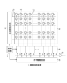
- FIG. 1 is a block diagram showing a schematic configuration of a solid-state imaging device according to one embodiment
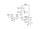
- FIG. 3 is a circuit diagram of each pixel in the pixel array section
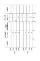
- FIG. 4 is a timing chart showing imaging timings of pixels
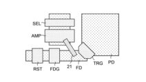
- FIG. 2 is a layout diagram of a circuit portion of a pixel
- FIG. 4 is a cross-sectional view of the vicinity of an FD wiring and an amplification transistor
- FIG. 4 is a cross-sectional view of the vicinity of the FD wiring and the gate of the gain switching transistor; The figure explaining a feedthrough.
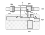
- FIG. 2 is a plan layout diagram of a circuit portion of a pixel according to the first embodiment
- FIG. 7 is a cross-sectional view taken along the line AB of FIG. 7
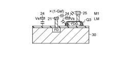
- FIG. 8 is a cross-sectional view taken along the line CD of FIG. 7;
- FIG. 8 is a layout diagram according to a modified example of FIG. 7 ;
- FIG. 10 is a sectional view taken along the line CD of FIG. 9;
- FIG. 7 is a layout diagram of a circuit portion of a pixel according to the second embodiment;
- FIG. 11 is a sectional view along line AB of FIG. 11;
- FIG. 11 is a layout diagram of a circuit portion of a pixel according to the third embodiment;
- FIG. 13 is a cross-sectional view along the line AB of FIG. 13;
- FIG. 14 is a layout diagram according to a modified example of FIG. 13 ;
- FIG. 15 is a cross-sectional view along the line AB of FIG. FIG.
- FIG. 11 is a circuit diagram showing a configuration example of a pixel in the fifth embodiment
- 1 is a block diagram showing an example of a schematic configuration of a vehicle control system
- FIG. FIG. 2 is an explanatory diagram showing an example of installation positions of an information detection unit outside the vehicle and an imaging unit;
- solid-state imaging devices and electronic devices will be described with reference to the drawings.
- the solid-state imaging device and the electronic device may have components and functions that are not illustrated or described.
- the following description does not exclude components or features not shown or described.
- FIG. 1 is a block diagram showing a schematic configuration of a solid-state imaging device 1 according to one embodiment of the present disclosure.
- the solid-state imaging device 1 of FIG. 1 includes a pixel array section 2, a vertical drive circuit 3, a column signal processing circuit 4, a horizontal drive circuit 5, an output circuit 6, and a control circuit .
- the pixel array section 2 includes a plurality of pixels 10 arranged in row and column directions, a plurality of signal lines L1 extending in the column direction, and a plurality of row selection lines L2 extending in the row direction. have.
- the vertical drive circuit 3 drives a plurality of row selection lines L2. More specifically, the vertical drive circuit 3 line-sequentially supplies drive signals to the plurality of row selection lines L2 to line-sequentially select each row selection line L2.
- a plurality of signal lines L1 extending in the column direction are connected to the column signal processing circuit 4 .
- the column signal processing circuit 4 analog-digital (AD) converts a plurality of pixel signals supplied via a plurality of signal lines L1. More specifically, the column signal processing circuit 4 compares the pixel signal on each signal line L1 with the reference signal, and converts the digital pixel signal based on the time until the signal levels of the pixel signal and the reference signal match. Generate.
- the column signal processing circuit 4 sequentially generates a digital pixel signal (P-phase signal) at the reset level of the floating diffusion layer in the pixel and a digital pixel signal (D-phase signal) at the pixel signal level, and performs correlated double sampling ( CDS: Correlated Double Sampling).
- the horizontal drive circuit 5 controls the timing of transferring the output signal of the column signal processing circuit 4 to the output circuit 6 .
- the control circuit 7 controls the vertical drive circuit 3, the column signal processing circuit 4, and the horizontal drive circuit 5.
- the control circuit 7 generates a reference signal that the column signal processing circuit 4 uses for AD conversion.
- FIG. 2 is a circuit diagram of each pixel 10 in the pixel array section 2.
- FIG. The pixel 10 in FIG. 2 includes a photodiode PD, a floating diffusion layer (FD), a transfer transistor (first transistor) Q1, an amplification transistor (second transistor) Q2, and a charge-voltage conversion gain switching transistor. It has (hereinafter referred to as a gain switching transistor, third transistor) Q3, a reset transistor (third transistor) Q4, a selection transistor Q5, and an exhaust transistor Q6.
- Each transistor Q1-Q6 in the pixel 10 is, for example, an NMOS (N-channel Metal Oxide Semiconductor) transistor.
- the photodiode PD accumulates charges obtained by photoelectrically converting incident light.
- the transfer transistor Q1 transfers the charge accumulated in the photodiode PD to the floating diffusion layer FD when the transfer gate TRG is high.
- a gate AMP of the amplification transistor Q2 is set to a potential corresponding to the accumulated charges in the floating diffusion layer FD.
- the source of the amplification transistor Q2 is connected to the drain of the selection transistor Q5, and the source of the selection transistor Q5 is connected to the signal line L1.
- the amplification transistor Q2 and the selection transistor Q5 constitute a source follower circuit, and the potential of the signal line L1 fluctuates according to the potential of the floating diffusion layer FD.
- the source of the gain switching transistor Q3 is connected to the floating diffusion layer FD, and the drain is connected to the source of the reset transistor Q4 and to one end of the pixel internal capacitance C1.
- a conversion gain switching signal is input to the gate FDG of the gain switching transistor Q3.
- the gain switching transistor Q3 When the conversion gain switching signal becomes high, the gain switching transistor Q3 is turned on, the floating diffusion layer FD and the pixel internal capacitance C1 are connected in parallel, and the capacity capable of accumulating the photoelectrically converted charges increases. lower.
- the gain switching transistor Q3 is turned off, photoelectrically converted charges are accumulated only in the floating diffusion layer FD, so that the conversion gain increases.
- the HCG drive mode is selected, for example, when shooting in a dark place.
- FIG. 3 is a timing chart showing imaging timing of the pixel 10.
- FIG. FIG. 3 shows the on/off timings of the transistors Q1, Q3, Q4, and Q5 in the pixel 10 in the HCG drive mode and the LCG drive mode.
- Each pixel 10 in the pixel array section 2 is driven row by row by a row selection signal.
- Times t1 to t2, t2 to t3, and t3 to t7 in FIG. 3 are each one horizontal period, and one pixel row is read out during one horizontal period.
- FIG. 3 shows imaging timings for a specific pixel row.
- a charge discharge operation for a specific pixel row is performed within one horizontal period from time t1 to t2 in the HCG drive mode.
- the reset transistor Q4 is turned on for a predetermined period
- the gain switching transistor Q3 is turned on while the reset transistor Q4 is on
- the transfer transistor Q1 is turned on while the gain switching transistor Q3 is on.
- the charges accumulated in the floating diffusion layer FD are discharged to the power supply voltage node VDD via the gain switching transistor Q3 and the reset transistor Q4.
- the transfer transistor Q1 while the transfer transistor Q1 is on, the accumulated charges in the photodiode PD and the accumulated charges in the floating diffusion layer FD are discharged to the power supply voltage node VDD via the gain switching transistor Q3 and the reset transistor Q4.
- charge accumulation is performed by photoelectric conversion of a specific pixel row.
- pixel signals of a specific pixel row are read out to the signal line L1.
- the gate signal SEL of the select transistor Q5 goes high between times t3-t7.
- the gate FDG of gain switching transistor Q3 is turned on for a predetermined period from time t4.
- Transfer transistor Q1 is off between times t4 and t5.
- the reset transistor Q4 is continuously turned on from time t4 to t6, and the gain switching transistor Q3 is turned on for a predetermined period from time t4.
- the charges accumulated in the floating diffusion layer FD are discharged to the power supply voltage node VDD, and the potential of the floating diffusion layer FD becomes the reset level.
- the reset level of the floating diffusion layer FD is read out to the signal line L1 through the amplification transistor Q2 and selection transistor Q5.
- the transfer gate TRG is turned on for a predetermined period. Between times t5 and t6, the reset transistor Q4 is on, but the gain switching transistor Q3 is off. stored in Therefore, the floating diffusion layer FD has a potential corresponding to the photoelectrically converted charge, and a pixel signal (D-phase signal) corresponding to the photoelectrically converted charge is read out to the signal line L1 between times t5 and t6. .
- the timing from time t3 to t7 differs from that in the HCG drive mode.
- the reset transistor Q4 is turned on for a predetermined period from time t4, and the gain switching transistor Q3 is continuously turned on from time t4 to t6.
- the readout of the P-phase signal from time t4 to t5 is performed in the same manner as in the HCG drive mode, but when the D-phase signal is read out thereafter, the charge photoelectrically converted by the photodiode PD is It is accumulated in the floating diffusion layer FD and the pixel content C1. Therefore, since the FD capacitance is increased, the potential fluctuation of the floating diffusion layer FD is suppressed, and the gain by the amplification transistor Q2 is suppressed low.
- the wiring connecting the floating diffusion layer FD and the gate of the amplification transistor Q2 may cause capacitive coupling with the gate FDG of the gain switching transistor Q3.
- FIG. 4 is a layout diagram of the circuit portion of the pixel 10.
- a transfer gate TRG is arranged across the photodiode PD and the floating diffusion layer FD.
- the FD wiring 21 connected to the gate AMP of the amplification transistor Q2 and the floating diffusion layer FD is arranged close to the gate FDG of the gain switching transistor Q3, causing capacitive coupling.
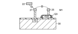
- FIG. 5A and 5B are schematic cross-sectional views of the circuit portion of the pixel 10.
- FIG. 5A shows a cross-sectional structure near the FD wiring 21 and the amplifier transistor Q2
- FIG. 5B shows a cross-sectional structure near the FD wiring 21 and the gate FDG of the gain switching transistor Q3.
- an FD wiring 21 is arranged above the floating diffusion layer FD and the amplification transistor Q2, and the FD wiring 21 is connected to the floating diffusion layer FD and the gate AMP of the amplification transistor Q2 via contacts, respectively.
- Another wiring layer 22 and a conductive member are arranged in the vicinity of the FD wiring 21, and capacitive coupling occurs between them.
- the capacitive coupling of the FD wiring 21 increases the total capacitance of the floating diffusion layer FD and reduces the conversion gain.
- the feed-through becomes large at the time of resetting the floating diffusion layer FD, which induces a charge transfer failure.
- the proportion of the FD capacitance occupied by capacitive coupling increases, resulting in a larger feedthrough. Therefore, in order to achieve both low noise and charge transfer, it is desirable to reduce capacitive coupling between the FD wiring 21 and the gate wiring (FDG wiring) of the gain switching transistor Q3.
- FIG. 6 is a diagram for explaining feedthrough, showing potential relationships among the transfer transistor Q1, the gain switching transistor Q3, and the reset transistor Q4.
- the vertical axis in FIG. 6 represents potential, and indicates that the lower the position, the higher the potential.
- FIG. 6 shows changes in the potential well caused by potential changes in the gate TRG of the transfer transistor Q1, the gate FDG of the gain switching transistor Q3, and the gate RST of the reset transistor Q4.
- ST1 in FIG. 6 shows the state before the floating diffusion layer FD is reset. In this state, the gain switching transistor Q3 and the reset transistor Q4 are both off, and the transfer transistor Q1 is also off.
- ST2 is the state in which the floating diffusion layer FD is set to the reset level. In this state, since both the gain switching transistor Q3 and the reset transistor Q4 are turned on, the accumulated charges in the floating diffusion layer FD are discharged to the power supply voltage node VDD.
- ST3 is a state in which the reset transistor Q4 is turned off while the gain switching transistor Q3 remains on.
- ST2 and ST3 show operations during resetting of the floating diffusion layer FD.
- ST4 is a state in which the reset operation of the floating diffusion layer FD is completed. In this state, both the gain switching transistor Q3 and the reset transistor Q4 are turned off. In this state, if the FD wiring 21 and the gate wiring of the gain switching transistor Q3 are capacitively coupled, the charge stored in the floating diffusion layer FD increases by the amount corresponding to the capacitive coupling, and the potential of the floating diffusion layer FD becomes , is reduced by ⁇ Vn represented by the following equation (1).
- Equation (1) CFD is the capacitance of the FD wiring 21
- CFDG is the capacitive coupling between the FD wiring 21 and the gate wiring of the gain switching transistor Q3
- ⁇ VFDG is the amount of change in the gate potential of the gain switching transistor Q3.
- ST5 is the state in which charge transfer is started. In this state, the transfer transistor Q1 is turned on, and the charge accumulated in the photodiode PD is transferred to the floating diffusion layer FD. Accumulated charges in the diffusion layer FD flow back to the photodiode PD. This is the phenomenon called feedthrough described above.
- ST6 is the state where the charge transfer ends. In this state, the transfer transistor Q1 is turned off. Since the charges accumulated in the floating diffusion layer FD flow back to the photodiode PD in ST5, charges that could not be transferred to the floating diffusion layer FD remain in the photodiode PD.
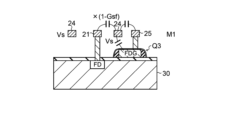
- FIG. 8A is a cross-sectional view taken along line AB of FIG. 7
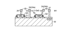
- FIG. 8B is a cross-sectional view along line CD of FIG.
- the transfer gate TRG of the transfer transistor Q1, the gate FDG of the gain switching transistor Q3, and the gate RST of the reset transistor Q4 are arranged near the floating diffusion layer FD.
- An FD wiring 21 is arranged from the floating diffusion layer FD to the gate AMP of the amplification transistor Q2.
- a selection transistor Q5 is arranged in the vicinity of the amplification transistor Q2.
- a new wiring layer (hereinafter referred to as a Vs wiring or wiring layer) 24 is provided in the vicinity of the FD wiring 21 so as to cause capacitive coupling with the FD wiring 21 and conduct to the source of the gain switching transistor Q3. .
- the Vs wiring 24 is routed so as to surround the FD wiring 21, but the layout arrangement does not necessarily have to be the same as in FIG.
- the Vs wiring 24 is electrically connected to the source of the amplification transistor Q2 via a contact 20 provided at one location.
- the Vs wiring 24 is electrically connected to nowhere other than this contact 20 . That is, the Vs wiring 24 is connected to the source of one amplification transistor Q2 at only one point and routed around the FD wiring 21 .
- the Vs wiring 24 is arranged between the FD wiring 21 and the wiring layer (hereinafter referred to as FDG wiring) 25 connected to the gate FDG of the gain switching transistor Q3. ing. Therefore, capacitive coupling occurs between the FD wiring 21 and the FDG wiring 25 in the conventional art, whereas capacitive coupling occurs between the FD wiring 21 and the Vs wiring 24 in the present embodiment. At the same time, capacitive coupling also occurs between the FDG wiring 25 and the Vs wiring 24 . 8A and 8B, the FD wiring 21, the Vs wiring 24, and the FDG wiring 25 are covered with an insulating layer.
- the amplification transistor Q2 performs a source follower operation, the potential of the FD wiring 21 and the potential of the Vs wiring 24 change together, and the capacitance due to capacitive coupling between the FD wiring 21 and the Vs wiring 24 is (1 -Gst) is multiplied. Since the source follower gain Gst is approximately 0.8, the capacitance due to capacitive coupling between the FD wiring 21 and the Vs wiring 24 is sufficiently small.
- the capacitive coupling between the FD wiring 21 and the FDG wiring 25 can be substantially shielded, and the capacitance of the floating diffusion layer FD can be reduced. (hereinafter referred to as FD capacity) can be reduced, and the charge-voltage conversion efficiency can be improved. Further, according to the present embodiment, since the FD capacitance is reduced, the charges in the floating diffusion layer FD can be sufficiently discharged to the power supply voltage node VDD when the floating diffusion layer FD is reset, and feedthrough can be reduced. Therefore, it is possible to achieve both low noise and suppression of transfer failure by increasing the conversion gain.
- the Vs wiring 24 is arranged in the same wiring layer as the FD wiring 21 and the FDG wiring 25 (for example, the M1 wiring layer), but the Vs wiring 24 is arranged in a wiring layer different from the FD wiring 21 and the FDG wiring 25. may be placed. If the Vs wiring 24 is arranged in the vicinity of the FD wiring 21 and the Vs wiring 24 is arranged in the vicinity of the FDG wiring 25, the wiring area in which the Vs wiring 24 is provided does not matter.
- a wiring layer (hereinafter referred to as SEL wiring) 26 connected to the gate SEL of the select transistor Q5 and a wiring layer (VDD wiring) 27 connected to the power supply voltage node VDD.
- VDD wiring wiring layer
- a Vs wiring 24 is arranged between them.
- two Vs wires 24 separated from each other are arranged in the cross section of FIG. 8B, in reality, they are a continuous Vs wire 24 as shown in FIG.
- the two wiring portions separated by the cross section of FIG. 8B are hereinafter referred to as a first Vs wiring portion 24a and a second Vs wiring portion 24b.
- Vs wiring 24 were not present, capacitive coupling would occur between the gate of the amplification transistor Q2, which has the same potential as the floating diffusion layer FD, and the wiring (VDD wiring 27) connected to the power supply voltage node VDD. and the wiring (hereinafter referred to as SEL wiring 26) connected to the gate of the selection transistor Q5 cause capacitive coupling.
- the capacitance due to capacitive coupling between the first Vs wiring portion 24a or the second Vs wiring portion 24b and the gate AM of the amplification transistor Q2 is multiplied by (1-Gsf). Since the source follower gain Gsf is about 0.8, each capacitive coupling mentioned above is a small value.
- capacitive coupling between the SEL wiring 26 and the gate AMP of the amplification transistor Q2 and capacitive coupling between the VDD wiring 27 and the gate AMP of the amplification transistor Q2 can be shielded, thereby reducing the capacitance of the FD wiring 21. be able to.
- the Vs wiring 24 is arranged in the same wiring layer (for example, M1 wiring layer) as the SEL wiring 26 and the VDD wiring 27, but the Vs wiring 24 is arranged in a wiring layer different from that of the SEL wiring 26 and the VDD wiring 27. may be placed. However, the Vs wiring 24 must be arranged near the SEL wiring 26 and the VDD wiring 27 .
- the Vs wiring 24 By arranging the Vs wiring 24 as shown in FIGS. 8A and 8B, not a little capacitive coupling occurs between the Vs node and the floating diffusion layer FD. Therefore, in order to maximize the effect of reducing the FD capacitance while shielding the capacitive coupling between the FD wiring 21 and other wirings, the Vs wiring 24 should be placed as close to the wiring to be shielded as possible within the range allowed by the design rules. desirable.
- FIG. 9 is a layout diagram according to a modified example of FIG. 7, and FIG. 10 is a cross-sectional view taken along the line CD of FIG.
- a conductive member 28 such as a wiring layer connected to a portion other than the gate may be arranged above the gate of the amplification transistor.
- the gate of the amplification transistor Q2 and the conductive member 28 cause capacitive coupling, which can be a factor in increasing the FD capacitance. Therefore, as shown in FIG. 10, the Vs wiring 24 may be arranged between the gate of the amplification transistor Q2 and the conductive member 28 thereabove.
- the capacitive coupling between the gate of the amplification transistor Q2 and the conductive member 28 can be blocked while the Vs wiring 24 and the gate of the amplification transistor Q2 generate capacitive coupling, thereby reducing the FD capacitance. can be done.
- part of the Vs wiring 24 is displaced according to the position of the conductive member 28.
- the Vs wiring 24 in FIG. 10 is desirably arranged so as to overlap with the conductive member 28 in plan view.
- the Vs wiring 24 is arranged in the same wiring layer as the SEL wiring 26 and the VDD wiring 27 (for example, the M1 wiring layer), but the Vs wiring 24 is arranged in a wiring layer different from the SEL wiring 26 and the VDD wiring 27. can be placed in
- the Vs wiring 24 connected to the source of the amplification transistor Q2 is newly provided, the Vs wiring 24 is routed, and the Vs wiring 24 is arranged between the FD wiring 21 and the FDG wiring 25. Therefore, capacitive coupling between the FD wiring 21 and the FDG wiring 25 can be shielded, and the FD capacitance can be reduced. Further, in the first embodiment, the Vs wiring 24 is arranged between the gate AMP of the amplification transistor Q2 and the VDD wiring 27, and the Vs wiring 24 is also arranged between the gate AMP of the amplification transistor Q2 and the SEL wiring 26. do. Thereby, the FD capacity can be further reduced.
- the FD capacitance can be reduced, and the charges in the floating diffusion layer FD can be sufficiently discharged to the power supply voltage node VDD when the floating diffusion layer FD is reset. Therefore, feedthrough is reduced, and transmission failure can be suppressed while reducing noise by increasing conversion gain.
- the Vs wiring 24 is arranged in the same wiring layer as the FD wiring 21 and the FDG wiring 25. However, the Vs wiring 24 is arranged in a wiring layer region with a height different from that of the FD wiring 21. , FD wiring 21 can be shielded.
- FIG. 11 is a layout diagram of the circuit portion of the pixel 10 according to the second embodiment
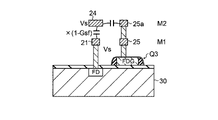
- FIG. 12 is a sectional view taken along line AB of FIG.
- Vs wiring 24 is arranged above FD wiring 21 . Without the Vs wiring 24 , the FD wiring 21 causes capacitive coupling with the FDG wiring 25 .
- FIG. 12 by arranging the Vs wiring 24 above the FD wiring 21, the FD wiring 21 and the Vs wiring 24 cause capacitive coupling, and the FD wiring 21 and the FDG wiring 25 can shield the capacitive coupling between
- the FDG wiring 25 has a two-layer structure, and the upper wiring layer 25a is provided in the same wiring region as the Vs wiring 24 (for example, the M2 wiring layer). 24 can cause capacitive coupling, and the capacitive coupling between the FD wiring 21 and the FDG wiring 25 can be further shielded.
- Vs wiring 24 By arranging the Vs wiring 24 above the FD wiring 21, it is possible to shield capacitive coupling between the FD wiring 21 and a conductive member arranged further above.
- the FD wiring 21 and the FDG wiring 25 are arranged in the M1 wiring layer, and the Vs wiring 24 is arranged in the M2 wiring layer.
- the places where they are provided are not necessarily limited to the M1 wiring layer and the M2 wiring layer.
- the FD wiring 21 is substantially removed by arranging the Vs wiring 24 above the FD wiring 21. Shielding is possible, and an effect of shielding capacitive coupling between the FD wiring 21 and the FDG wiring 25 is obtained.
- the FD wiring 21 is arranged in the M1 wiring layer, but the FD wiring 21 may be arranged in a position closer to the semiconductor substrate 30 than the M1 wiring layer. Possible.
- a wiring layer located closer to the semiconductor substrate 30 than the M1 wiring layer is called a local wiring layer LW for convenience.
- a photodiode PD and a floating diffusion layer FD are arranged on the semiconductor substrate 30 .
- the circuit of the pixel 10 is arranged on the front side of the semiconductor substrate 30 .
- the local wiring layer LW is provided at a position close to the surface of the semiconductor substrate 30 .
- the distance from other wiring layers is increased, so that capacitive coupling is reduced.
- the distance to the gate of the transistor located near the FD wiring 21 is shortened, capacitive coupling with this transistor is significantly increased.
- the Vs wiring 24 is provided in the local wiring layer LW near the FD wiring 21 to cause capacitive coupling with the FD wiring 21 .
- FIG. 13 is a layout diagram of the circuit portion of the pixel 10 according to the third embodiment
- FIG. 14 is a sectional view taken along line AB of FIG.
- the Vs wiring 24 according to the third embodiment is substantially the same as the Vs wiring 24 in FIG. 7 in plan layout.
- the Vs wiring 24 according to the third embodiment is arranged in the local wiring layer LW closer to the semiconductor substrate 30 than the M1 wiring layer, as shown in FIG.
- the FD wiring 21 is also arranged in the local wiring layer LW.
- the Vs wiring 24 is arranged between the FD wiring 21 and the gate of the gain switching transistor Q3.
- the FD wiring 21 and the Vs wiring 24 cause capacitive coupling
- the Vs wiring 24 and the FDG wiring 25 cause capacitive coupling.
- capacitive coupling between the FD wiring 21 and the gate of the gain switching transistor Q3 can be shielded.
- Vs wiring 24 it is desirable to place the Vs wiring 24 as close to the FD wiring 21 as possible. By bringing the Vs wiring 24 closer to the FD wiring 21, the Vs wiring 24 and the FD wiring 21 are reliably capacitively coupled. Moreover, it is desirable to arrange the Vs wiring 24 as close to the gate of the gain switching transistor Q3 and the FDG wiring 25 as possible. By bringing the Vs wiring 24 close to the gate of the gain switching transistor Q3 and the FDG wiring 25, the Vs wiring 24 reliably causes capacitive coupling with the gate of the gain switching transistor Q3 and the FDG wiring 25.
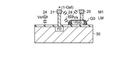
- FIG. 15 is a layout diagram according to a modified example of FIG. 13, and FIG. 16 is a sectional view taken along the line AB of FIG.
- a modified example is the same as FIG. 14 in that the Vs wiring 24 is provided in the local wiring layer LW, but differs from FIG. 14 in that the FD wiring 21 is arranged in the M1 wiring layer.
- the Vs wire 24 causes capacitive coupling with the FD wire 21
- the Vs wire 24 causes capacitive coupling with the gate of the gain switching transistor Q3
- the Vs wire 24 capacitively couples with the FDG gate. give rise to a ring.
- the wiring layers forming the circuit of the pixel 10 are formed in existing wiring layers such as the M1 wiring layer and the M2 wiring layer. In contrast, by forming only the newly provided Vs wiring 24 in the local wiring layer LW, the Vs wiring 24 is formed without affecting the layout arrangement of the existing pixel 10 circuit, thereby reducing the FD capacitance. can.
- the FD wiring 21 may be arranged in the local wiring layer LW and the Vs wiring 24 may be arranged in the M1 wiring layer. Even in this case, the FD capacitance can be reduced because the Vs wiring 24 and the FD wiring 21 cause capacitive coupling.
- the Vs wiring 24 and the FD wiring 21 are provided in the local wiring layer LW provided at a position closer to the semiconductor substrate 30 than the existing wiring layers such as the M1 wiring layer and the M2 wiring layer.
- capacitive coupling can be generated between the FD wiring 21 and the Vs wiring 24, and the FD capacitance can be reduced.
- the charges in the floating diffusion layer FD can be sufficiently discharged to the power supply voltage node VDD when the floating diffusion layer FD is reset, and feedthrough can be reduced.
- Capacitive coupling may occur with a wiring (hereinafter referred to as an RST wiring) connected to the gate of the .
- RST wiring a wiring
- Capacitive coupling also occurs between Thereby, the capacitive coupling between the FD wiring 21 and the Vs wiring 24 can be shielded, and the FD capacitance can be reduced.
- the charges in the floating diffusion layer FD can be discharged to the power supply voltage node VDD when the floating diffusion layer FD is reset, and the feedthrough can be reduced.
- a feature of the solid-state imaging device is that it employs a global shutter method.
- the global shutter method all pixels in the pixel array section 2 are exposed at the same timing, the P-phase signal level and the D-phase signal level are stored in the pixel 10, and the stored P-phase signal level and D-phase signal level are stored. The digital signals of the difference between are sequentially output. Adopting the global shutter method eliminates the distortion of the captured image due to the deviation of the exposure timing.
- FIG. 17 is a circuit diagram showing one configuration example of the pixel 10 according to the fifth embodiment of the present disclosure.
- circuit elements having functions common to those of FIG. 2 are given the same reference numerals.
- a pixel 10 in FIG. 17 includes a front-stage circuit 11, capacitive elements C11 and C12, a selection circuit 12, a rear-stage reset transistor Q4b, and a rear-stage circuit 13.
- FIG. 17 is a circuit diagram showing one configuration example of the pixel 10 according to the fifth embodiment of the present disclosure.
- circuit elements having functions common to those of FIG. 2 are given the same reference numerals.
- a pixel 10 in FIG. 17 includes a front-stage circuit 11, capacitive elements C11 and C12, a selection circuit 12, a rear-stage reset transistor Q4b, and a rear-stage circuit 13.
- the front-stage circuit 11 includes a photoelectric conversion element PD, a transfer transistor Q1, a floating diffusion layer FD, a reset transistor Q4a, a front-stage amplification transistor Q2, and a current source .
- the photoelectric conversion element PD generates charges by photoelectric conversion.
- the transfer transistor Q ⁇ b>1 transfers charges from the photoelectric conversion element PD to the floating diffusion layer FD according to the transfer signal TRG from the vertical drive circuit 3 .
- the reset transistor Q4a is initialized by extracting charges from the floating diffusion layer FD according to the FD reset signal RSTa from the vertical drive circuit 3.
- the floating diffusion layer FD accumulates charges and generates a voltage corresponding to the amount of charges.
- the front-stage amplifying transistor Q2 amplifies the voltage level of the floating diffusion layer FD and outputs it to the front-stage node n1.
- the drain of the reset transistor Q4a and the drain of the pre-amplification transistor Q2 are connected to the power supply voltage VDD.
- Current source 14 is connected to the source of pre-amplifying transistor Q2. This current source 14 supplies the current id1 under the control of the vertical driving circuit 3.
- the selection circuit 12 includes a selection transistor Q5a and a selection transistor Q5b.
- the selection transistor Q5a opens and closes the path between the capacitive element C11 and the post-stage node n2 according to the selection signal ⁇ r from the vertical drive circuit 3 .
- the selection transistor Q5b opens and closes the path between the capacitive element C12 and the post-stage node n2 according to the selection signal ⁇ s from the vertical drive circuit 3 .
- the post-stage reset transistor Q4b initializes the level of the post-stage node n2 to a predetermined potential Vreg according to the post-stage reset signal RSTb from the vertical drive circuit 3.
- a potential different from the power supply potential VDD (for example, a potential lower than VDD) is set to the potential Vreg.
- the post-stage circuit 13 includes a post-amplification transistor Q2b and a post-stage selection transistor Q5c.
- the rear-stage amplification transistor Q2b amplifies the level of the rear-stage node n2.
- the post-stage amplifying transistor outputting to L1 is an example of the second amplifying transistor described in the claims.
- each transistor in the pixel 10 in FIG. 17 is an NMOS transistor.
- the vertical drive circuit 3 supplies a high-level FD reset signal RSTa and a transfer signal TRG to all pixels at the start of exposure. Thereby, the photoelectric conversion element PD is initialized.
- this control will be referred to as "PD reset”.
- the vertical drive circuit 3 supplies the high-level FD reset signal RSTa over the pulse period while setting the post-stage reset signal RSTb and the selection signal ⁇ r to high level for all pixels.
- the floating diffusion layer FD is initialized, and a level corresponding to the level of the floating diffusion layer FD at that time is held in the capacitive element C11. This control is hereinafter referred to as "FD reset".
- the level of the floating diffusion layer FD at the time of FD reset and the level corresponding to that level (holding level of the capacitive element C11 and level of the vertical signal line L1) are collectively referred to as “P phase” or “reset level” below. ”.
- the vertical drive circuit 3 supplies a high-level transfer signal TRG over the pulse period while setting the post-stage reset signal RSTb and the selection signal ⁇ s to high level for all pixels.
- signal charges corresponding to the amount of exposure are transferred to the floating diffusion layer FD, and a level corresponding to the level of the floating diffusion layer FD at that time is held in the capacitive element C12.
- phase D The level of the floating diffusion layer FD during signal charge transfer and the level corresponding thereto (the holding level of the capacitive element C12 and the level of the vertical signal line L1) are collectively referred to as “phase D” or “phase D” below. signal level”.
- the pixel 10 in FIG. 17 employs a global shutter method in which exposure of all pixels is started and ended at the same time.
- the pre-stage circuits 11 of all pixels sequentially generate a reset level and a signal level.
- the reset level is held in capacitive element C11
- the signal level is held in capacitive element C12.
- the vertical drive circuit 3 sequentially selects rows and sequentially outputs the reset level and signal level of the rows.
- the vertical drive circuit 3 supplies the high-level selection signal ⁇ r for a predetermined period while setting the FD reset signal RSTa and the post-stage selection signal SELb of the selected row to high level.
- the capacitive element C11 is connected to the post-stage node n2, and the reset level is read.
- the vertical drive circuit 3 After reading the reset level, the vertical drive circuit 3 supplies the high-level post-stage reset signal RSTb over the pulse period while keeping the FD reset signal RSTa and the post-stage selection signal SELb of the selected row at high level. As a result, the level of the subsequent node n2 is initialized. At this time, both the select transistor Q5a and the select transistor Q5b are in an open state, and the capacitive elements C11 and C12 are disconnected from the subsequent node n2.
- the vertical drive circuit 3 After initializing the post-stage node n2, the vertical drive circuit 3 supplies the high-level selection signal ⁇ s for a predetermined period while keeping the FD reset signal RSTa and the post-stage selection signal SELb of the selected row at high level. As a result, the capacitive element C12 is connected to the post-stage node n2, and the signal level is read out.
- the selection circuit 12 of the selected row performs control to connect the capacitive element C11 to the post-stage node n2, control to disconnect the capacitive elements C11 and C12 from the post-stage node n2, and control to disconnect the capacitive element C12 from the post-node n2. and control to connect to .
- the post-stage reset transistor Q4b of the selected row initializes the level of the post-stage node n2.
- the post-stage circuit 13 of the selected row sequentially reads out the reset level and the signal level from the capacitive elements C11 and C12 via the post-stage node n2, and outputs them to the vertical signal line L1.
- the Vs wiring 24 connected to the source of the pre-amplification transistor Q2a connects the floating diffusion layer FD and the FD wiring 21 connected to the gate of the pre-amplification transistor Q2a.
- a Vs wiring 24 is arranged between the FD wiring 21 and the gate wiring of the reset transistor Q4a.
- the capacitive coupling between the FD wiring 21 and the FDG wiring 25 can be shielded, and the FD capacitance can be reduced.
- the pixel 10 in FIG. 17 is not provided with a gain switching transistor, a gain switching transistor may be provided. When the gain switching transistor is provided, the FD capacitance can be reduced by placing the Vs wiring 24 between the gate wiring of the gain switching transistor and the FD wiring 21 .
- the technology (the present technology) according to the present disclosure can be applied to various products.
- the technology according to the present disclosure can be realized as a device mounted on any type of moving body such as automobiles, electric vehicles, hybrid electric vehicles, motorcycles, bicycles, personal mobility, airplanes, drones, ships, and robots. may
- FIG. 18 is a block diagram showing a schematic configuration example of a vehicle control system, which is an example of a mobile control system to which the technology according to the present disclosure can be applied.
- a vehicle control system 12000 includes a plurality of electronic control units connected via a communication network 12001.
- the vehicle control system 12000 includes a driving system control unit 12010, a body system control unit 12020, a vehicle exterior information detection unit 12030, a vehicle interior information detection unit 12040, and an integrated control unit 12050.
- a microcomputer 12051, an audio/image output unit 12052, and an in-vehicle network I/F (Interface) 12053 are illustrated as the functional configuration of the integrated control unit 12050.
- the drive system control unit 12010 controls the operation of devices related to the drive system of the vehicle according to various programs.
- the driving system control unit 12010 includes a driving force generator for generating driving force of the vehicle such as an internal combustion engine or a driving motor, a driving force transmission mechanism for transmitting the driving force to the wheels, and a steering angle of the vehicle. It functions as a control device such as a steering mechanism to adjust and a brake device to generate braking force of the vehicle.
- the body system control unit 12020 controls the operation of various devices equipped on the vehicle body according to various programs.
- the body system control unit 12020 functions as a keyless entry system, a smart key system, a power window device, or a control device for various lamps such as headlamps, back lamps, brake lamps, winkers or fog lamps.
- the body system control unit 12020 can receive radio waves transmitted from a portable device that substitutes for a key or signals from various switches.
- the body system control unit 12020 receives the input of these radio waves or signals and controls the door lock device, power window device, lamps, etc. of the vehicle.
- the vehicle exterior information detection unit 12030 detects information outside the vehicle in which the vehicle control system 12000 is installed.
- the vehicle exterior information detection unit 12030 is connected with an imaging section 12031 .
- the vehicle exterior information detection unit 12030 causes the imaging unit 12031 to capture an image of the exterior of the vehicle, and receives the captured image.
- the vehicle exterior information detection unit 12030 may perform object detection processing or distance detection processing such as people, vehicles, obstacles, signs, or characters on the road surface based on the received image.
- the imaging unit 12031 is an optical sensor that receives light and outputs an electrical signal according to the amount of received light.
- the imaging unit 12031 can output the electric signal as an image, and can also output it as distance measurement information.
- the light received by the imaging unit 12031 may be visible light or non-visible light such as infrared rays.
- the in-vehicle information detection unit 12040 detects in-vehicle information.
- the in-vehicle information detection unit 12040 is connected to, for example, a driver state detection section 12041 that detects the state of the driver.
- the driver state detection unit 12041 includes, for example, a camera that captures an image of the driver, and the in-vehicle information detection unit 12040 detects the degree of fatigue or concentration of the driver based on the detection information input from the driver state detection unit 12041. It may be calculated, or it may be determined whether the driver is dozing off.
- the microcomputer 12051 calculates control target values for the driving force generator, the steering mechanism, or the braking device based on the information inside and outside the vehicle acquired by the vehicle exterior information detection unit 12030 or the vehicle interior information detection unit 12040, and controls the drive system control unit.
- a control command can be output to 12010 .
- the microcomputer 12051 realizes the functions of ADAS (Advanced Driver Assistance System) including collision avoidance or shock mitigation of vehicles, follow-up driving based on inter-vehicle distance, vehicle speed maintenance driving, vehicle collision warning, vehicle lane deviation warning, etc. Cooperative control can be performed for the purpose of ADAS (Advanced Driver Assistance System) including collision avoidance or shock mitigation of vehicles, follow-up driving based on inter-vehicle distance, vehicle speed maintenance driving, vehicle collision warning, vehicle lane deviation warning, etc. Cooperative control can be performed for the purpose of ADAS (Advanced Driver Assistance System) including collision avoidance or shock mitigation of vehicles, follow-up driving based on inter-vehicle distance, vehicle speed maintenance driving
- the microcomputer 12051 controls the driving force generator, the steering mechanism, the braking device, etc. based on the information about the vehicle surroundings acquired by the vehicle exterior information detection unit 12030 or the vehicle interior information detection unit 12040, so that the driver's Cooperative control can be performed for the purpose of autonomous driving, etc., in which vehicles autonomously travel without depending on operation.
- the microcomputer 12051 can output a control command to the body system control unit 12030 based on the information outside the vehicle acquired by the information detection unit 12030 outside the vehicle.
- the microcomputer 12051 controls the headlamps according to the position of the preceding vehicle or the oncoming vehicle detected by the vehicle exterior information detection unit 12030, and performs cooperative control aimed at anti-glare such as switching from high beam to low beam. It can be carried out.
- the audio/image output unit 12052 transmits at least one of audio and/or image output signals to an output device capable of visually or audibly notifying the passengers of the vehicle or the outside of the vehicle.
- an audio speaker 12061, a display unit 12062, and an instrument panel 12063 are illustrated as output devices.
- the display unit 12062 may include at least one of an on-board display and a head-up display, for example.
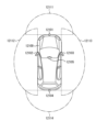
- FIG. 19 is a diagram showing an example of the installation position of the imaging unit 12031.
- the imaging unit 12031 has imaging units 12101, 12102, 12103, 12104, and 12105.
- the imaging units 12101, 12102, 12103, 12104, and 12105 are provided at positions such as the front nose, side mirrors, rear bumper, back door, and windshield of the vehicle 12100, for example.
- An image pickup unit 12101 provided in the front nose and an image pickup unit 12105 provided above the windshield in the passenger compartment mainly acquire images in front of the vehicle 12100 .
- Imaging units 12102 and 12103 provided in the side mirrors mainly acquire side images of the vehicle 12100 .
- An imaging unit 12104 provided in the rear bumper or back door mainly acquires an image behind the vehicle 12100 .
- the imaging unit 12105 provided above the windshield in the passenger compartment is mainly used for detecting preceding vehicles, pedestrians, obstacles, traffic lights, traffic signs, lanes, and the like.
- FIG. 19 shows an example of the imaging range of the imaging units 12101 to 12104.
- the imaging range 12111 indicates the imaging range of the imaging unit 12101 provided in the front nose
- the imaging ranges 12112 and 12113 indicate the imaging ranges of the imaging units 12102 and 12103 provided in the side mirrors, respectively
- the imaging range 12114 The imaging range of an imaging unit 12104 provided on the rear bumper or back door is shown. For example, by superimposing the image data captured by the imaging units 12101 to 12104, a bird's-eye view image of the vehicle 12100 viewed from above can be obtained.
- At least one of the imaging units 12101 to 12104 may have a function of acquiring distance information.
- at least one of the imaging units 12101 to 12104 may be a stereo camera composed of a plurality of imaging elements, or may be an imaging element having pixels for phase difference detection.
- the microcomputer 12051 determines the distance to each three-dimensional object within the imaging ranges 12111 to 12114 and changes in this distance over time (relative velocity with respect to the vehicle 12100). , it is possible to extract, as the preceding vehicle, the closest three-dimensional object on the traveling path of the vehicle 12100, which runs at a predetermined speed (for example, 0 km/h or more) in substantially the same direction as the vehicle 12100. can. Furthermore, the microcomputer 12051 can set the inter-vehicle distance to be secured in advance in front of the preceding vehicle, and perform automatic brake control (including following stop control) and automatic acceleration control (including following start control). In this way, cooperative control can be performed for the purpose of automatic driving in which the vehicle runs autonomously without relying on the operation of the driver.
- automatic brake control including following stop control
- automatic acceleration control including following start control
- the microcomputer 12051 converts three-dimensional object data related to three-dimensional objects to other three-dimensional objects such as motorcycles, ordinary vehicles, large vehicles, pedestrians, and utility poles. It can be classified and extracted and used for automatic avoidance of obstacles. For example, the microcomputer 12051 distinguishes obstacles around the vehicle 12100 into those that are visible to the driver of the vehicle 12100 and those that are difficult to see. Then, the microcomputer 12051 judges the collision risk indicating the degree of danger of collision with each obstacle, and when the collision risk is equal to or higher than the set value and there is a possibility of collision, an audio speaker 12061 and a display unit 12062 are displayed. By outputting an alarm to the driver via the drive system control unit 12010 and performing forced deceleration and avoidance steering via the drive system control unit 12010, driving support for collision avoidance can be performed.
- At least one of the imaging units 12101 to 12104 may be an infrared camera that detects infrared rays.
- the microcomputer 12051 can recognize a pedestrian by determining whether or not the pedestrian exists in the captured images of the imaging units 12101 to 12104 .
- recognition of a pedestrian is performed by, for example, a procedure for extracting feature points in images captured by the imaging units 12101 to 12104 as infrared cameras, and performing pattern matching processing on a series of feature points indicating the outline of an object to determine whether or not the pedestrian is a pedestrian.
- the audio image output unit 12052 outputs a rectangular outline for emphasis to the recognized pedestrian. is superimposed on the display unit 12062 . Also, the audio/image output unit 12052 may control the display unit 12062 to display an icon or the like indicating a pedestrian at a desired position.
- the technology according to the present disclosure can be applied to the imaging unit 12031 and the like among the configurations described above.
- the solid-state imaging device 1 of the present disclosure can be applied to the imaging unit 12031 .
- this technique can take the following structures.
- a photoelectric conversion unit that photoelectrically converts incident light and accumulates electric charges; a first transistor that transfers charges accumulated in the photoelectric conversion unit; a floating diffusion layer that retains charges transferred by the first transistor; a second transistor that amplifies the charge held in the floating diffusion layer; a conductive layer conducting to the floating diffusion layer; a wiring layer that causes capacitive coupling with the conductive layer and conducts to the source of the second transistor.
- the solid-state imaging device according to item 1. comprising a third transistor for switching the charge-to-voltage conversion gain or initializing the charge in the floating diffusion layer;
- the wiring layer and the conductive layer are arranged in layers different from each other in the stacking direction with an insulating layer interposed therebetween;
- the solid-state imaging device according to (8) wherein the wiring layer and the gate wiring layer connected to the gate of the third transistor are arranged in the same layer with an insulating layer interposed therebetween.
- the wiring layer and the conductive layer are arranged in the same layer with an insulating layer interposed therebetween;
- the solid-state imaging device according to (8), wherein the wiring layer and the gate wiring layer connected to the gate of the third transistor are arranged in layers different from each other in the stacking direction with an insulating layer interposed therebetween.
- a layer in which the gate of the third transistor is arranged is arranged in a layer closer to a substrate in which the photoelectric conversion unit and the floating diffusion layer are arranged than the wiring layer and the conductive layer, (11 ).
- the wiring layer and the conductive layer are arranged in a layer closer to the substrate on which the photoelectric conversion section and the floating diffusion layer are arranged than the gate wiring layer of the third transistor.
- the conductive layer and the gate wiring layer of the third transistor are arranged in the same layer with an insulating layer interposed therebetween;
- the wiring layer is arranged in a layer closer to a substrate on which the photoelectric conversion section and the floating diffusion layer are arranged than the conductive layer and the gate wiring layer of the third transistor.
- first and second capacitive elements a pre-stage circuit that sequentially generates a predetermined reset level and a signal level corresponding to the amount of exposure and causes the first and second capacitive elements to hold the signals; control to connect one of the first and second capacitive elements to a predetermined post-stage node; control to disconnect both the first and second capacitive elements from the post-stage node; a selection circuit that sequentially performs control for connecting the other to the subsequent node; a post-stage reset transistor that initializes the level of the post-stage node when both the first and second capacitive elements are disconnected from the post-stage node; a post-stage circuit that sequentially reads and outputs the reset level and the signal level from the first and second capacitive elements via the post-stage node;
- the pre-stage circuit according to any one of (1) to (16), including the photoelectric conversion section, the first transistor, the floating diffusion layer, the second transistor, the conductive layer, and the wiring layer.
- solid-state imaging device (18) a solid-state imaging device that outputs a pixel signal obtained by photoelectrically converting light incident on a pixel area; A signal processing unit that performs signal processing based on the pixel signal,
- the solid-state imaging device is a photoelectric conversion unit that photoelectrically converts incident light and accumulates electric charges; a first transistor that transfers charges accumulated in the photoelectric conversion unit; a floating diffusion layer that retains charges transferred by the first transistor; a second transistor that amplifies the charge held in the floating diffusion layer; a conductive layer conducting to the floating diffusion layer;
- An electronic device comprising: a wiring layer that causes capacitive coupling with the conductive layer and conducts to the source of the second transistor.
- 1 solid-state imaging device 2 pixel array section, 3 vertical drive circuit, 4 column signal processing circuit, 5 horizontal drive circuit, 6 output circuit, 7 control circuit, 10 pixels, 11 front stage circuit, 12 selection circuit, 13 rear stage circuit, 14 current source, 20 contact, 21 FD wiring, 21 conductive layer, 22 wiring layer, 24 Vs wiring, 24a first Vs wiring section, 24b second Vs wiring section, 25 FDG wiring, 26 SEL wiring, 27 VDD wiring, 28 conductive member, 30 Semiconductor substrate
Landscapes
- Engineering & Computer Science (AREA)
- Multimedia (AREA)
- Signal Processing (AREA)
- Solid State Image Pick-Up Elements (AREA)
- Transforming Light Signals Into Electric Signals (AREA)
Abstract
Description
前記光電変換部に蓄積された電荷を転送する第1トランジスタと、
前記第1トランジスタで転送された電荷を保持する浮遊拡散層と、
前記浮遊拡散層に保持された電荷を増幅する第2トランジスタと、
前記浮遊拡散層に導通する導電層と、
前記導電層と容量カップリングを生じさせるとともに、前記第2トランジスタのソースに導通する配線層と、を備える、固体撮像装置が提供される。
前記配線層は、前記コンタクト以外の導電部材とは距離を隔てて配置されてもよい。
前記配線層の少なくとも一部は、前記第3トランジスタのゲートと前記導電層との間に配置されてもよい。
前記配線層と前記第3トランジスタのゲートに繋がるゲート配線層とは、絶縁層を介して同一の層に配置されてもよい。
前記配線層と前記第3トランジスタのゲートに繋がるゲート配線層とは、絶縁層を介して積層方向に互いに異なる層に配置されてもよい。
前記配線層は、前記導電層と前記第3トランジスタのゲート配線層とは異なる層に配置されてもよい。
前記配線層は、前記第2トランジスタのゲートと前記導電部材との間の層に配置されてもよい。
所定のリセットレベルと露光量に応じた信号レベルとを順に生成して前記第1及び第2の容量素子のそれぞれに保持させる前段回路と、
前記第1及び第2の容量素子の一方を所定の後段ノードに接続する制御と前記第1及び第2の容量素子の両方を前記後段ノードから切り離す制御と前記第1及び第2の容量素子の他方を前記後段ノードに接続する制御とを順に行う選択回路と、
前記第1及び第2の容量素子の両方が前記後段ノードから切り離されたときに前記後段ノードのレベルを初期化する後段リセットトランジスタと、
前記後段ノードを介して前記リセットレベル及び前記信号レベルを前記第1及び第2の容量素子から順に読み出して出力する後段回路とを備え、
前記前段回路は、前記光電変換部、前記第1トランジスタ、前記浮遊拡散層、前記第2トランジスタ、前記導電層、及び前記配線層を有してもよい。
前記画素信号に基づいて信号処理を行う信号処理部と、を備え、
前記固体撮像装置は、
入射光を光電変換して電荷を蓄積する光電変換部と、
前記光電変換部に蓄積された電荷を転送する第1トランジスタと、
前記第1トランジスタで転送された電荷を保持する浮遊拡散層と、
前記浮遊拡散層に保持された電荷を増幅する第2トランジスタと、
前記浮遊拡散層に導通する導電層と、
前記導電層と容量カップリングを生じさせるとともに、前記第2トランジスタのソースに導通する配線層と、を有する、電子機器が提供されてもよい。

図7は第1の実施形態に係る画素10の回路部分の平面レイアウト図、図8Aは図7のA-B線断面図、図8Bは図7のC-D線断面図である。
第1の実施形態では、Vs配線24をFD配線21やFDG配線25と同じ配線層に配置する例を示したが、Vs配線24をFD配線21とは異なる高さの配線層領域に配置し、FD配線21をシールドすることも可能である。
第1及び第2の実施形態では、FD配線21がM1配線層に配置されている例を示したが、FD配線21は、M1配線層よりも半導体基板30に近い位置に配置される場合もありうる。本明細書では、M1配線層よりも半導体基板30に近い位置の配線層を便宜上、ローカル配線層LWと呼ぶ。
上述した第1~第3の実施形態では、画素10内に利得切替トランジスタQ3を備える例を説明したが、画素10内に利得切替トランジスタQ3が存在しない場合には、FD配線21とリセットトランジスタQ4のゲートに繋がる配線(以下、RST配線)との間に容量カップリングが生じうる。この場合、FD配線21とRST配線との間に、上述したVs配線24を配置することで、FD配線21とVs配線24との間に容量カップリングが生じ、かつRST配線とVs配線24との間にも容量カップリングが生じる。これにより、FD配線21とVs配線24との間の容量カップリングを遮蔽することができ、FD容量を低減できる。また、FD容量を低減することで、浮遊拡散層FDのリセット時に浮遊拡散層FDの電荷を電源電圧ノードVDDに排出することができ、フィードスルーを小さくできる。
第5の実施形態に係る固体撮像装置は、グローバルシャッタ方式を採用する点に特徴がある。グローバルシャッタ方式では、画素アレイ部2内の全画素が同タイミングで露光を行ってP相信号レベルとD相信号レベルを画素10内に記憶し、記憶されたP相信号レベルとD相信号レベルの差分のデジタル信号を順に出力する。グローバルシャッタ方式を採用することで、露光タイミングのずれによる撮像画像の歪みが生じなくなる。
本開示に係る技術(本技術)は、様々な製品へ応用することができる。例えば、本開示に係る技術は、自動車、電気自動車、ハイブリッド電気自動車、自動二輪車、自転車、パーソナルモビリティ、飛行機、ドローン、船舶、ロボット等のいずれかの種類の移動体に搭載される装置として実現されてもよい。
(1)入射光を光電変換して電荷を蓄積する光電変換部と、
前記光電変換部に蓄積された電荷を転送する第1トランジスタと、
前記第1トランジスタで転送された電荷を保持する浮遊拡散層と、
前記浮遊拡散層に保持された電荷を増幅する第2トランジスタと、
前記浮遊拡散層に導通する導電層と、
前記導電層と容量カップリングを生じさせるとともに、前記第2トランジスタのソースに導通する配線層と、を備える、固体撮像装置。
(2)前記配線層の電位と前記導電層の電位とは連動して変動する、(1)に記載の固体撮像装置。
(3)前記配線層と前記導電層とは、絶縁層を介して同一の層に配置される、(1)又は(2)に記載の固体撮像装置。
(4)前記配線層は、前記導電層よりも、前記光電変換部及び前記浮遊拡散層が配置される基板に近い層に配置される、(1)又は(2)に記載の固体撮像装置。
(5)前記配線層と前記第2トランジスタのソースとを接続する、積層方向に延びるコンタクトを備え、
前記配線層は、前記コンタクト以外の導電部材とは距離を隔てて配置される、(1)乃至(4)のいずれか一項に記載の固体撮像装置。
(6)前記配線層は、前記導電層の少なくとも一部を取り囲むように配置される、(1)乃至(5)のいずれか一項に記載の固体撮像装置。
(7)前記導電層は、前記浮遊拡散層に接続される第1端部と、前記第2トランジスタのゲートに接続される第2端部とを有する、(1)乃至(6)のいずれか一項に記載の固体撮像装置。
(8)電荷電圧変換利得を切り替えるか、又は前記浮遊拡散層の電荷を初期化する第3トランジスタを備え、
前記配線層の少なくとも一部は、前記第3トランジスタのゲートと前記導電層との間に配置される、(1)乃至(7)のいずれか一項に記載の固体撮像装置。
(9)前記配線層と、前記第3トランジスタのゲートに繋がるゲート配線層と、前記導電層とは、それぞれ絶縁層を介して同一の層に配置される、(8)に記載の固体撮像装置。
(10)前記配線層と前記導電層とは、絶縁層を介して積層方向に互いに異なる層に配置され、
前記配線層と前記第3トランジスタのゲートに繋がるゲート配線層とは、絶縁層を介して同一の層に配置される、(8)に記載の固体撮像装置。
(11)前記配線層と前記導電層とは、絶縁層を介して同一の層に配置され、
前記配線層と前記第3トランジスタのゲートに繋がるゲート配線層とは、絶縁層を介して積層方向に互いに異なる層に配置される、(8)に記載の固体撮像装置。
(12)前記第3トランジスタのゲートが配置される層は、前記配線層及び前記導電層よりも、前記光電変換部及び前記浮遊拡散層が配置される基板に近い層に配置される、(11)に記載の固体撮像装置。
(13)前記配線層と前記導電層とは、前記第3トランジスタのゲート配線層よりも、前記光電変換部及び前記浮遊拡散層が配置される基板に近い層に配置される、(11)に記載の固体撮像装置。
(14)前記導電層と前記第3トランジスタのゲート配線層とは、絶縁層を介して同一の層に配置され、
前記配線層は、前記導電層と前記第3トランジスタのゲート配線層とは異なる層に配置される、(8)に記載の固体撮像装置。
(15)前記配線層は、前記導電層と前記第3トランジスタのゲート配線層とよりも、前記光電変換部及び前記浮遊拡散層が配置される基板に近い層に配置される、(14)に記載の固体撮像装置。
(16)前記配線層及び前記第2トランジスタのゲートとは積層方向に異なる層に配置される導電部材を備え、
前記配線層は、前記第2トランジスタのゲートと前記導電部材との間の層に配置される、(1)乃至(15)のいずれか一項に記載の固体撮像装置。
(17)第1及び第2の容量素子と、
所定のリセットレベルと露光量に応じた信号レベルとを順に生成して前記第1及び第2の容量素子のそれぞれに保持させる前段回路と、
前記第1及び第2の容量素子の一方を所定の後段ノードに接続する制御と前記第1及び第2の容量素子の両方を前記後段ノードから切り離す制御と前記第1及び第2の容量素子の他方を前記後段ノードに接続する制御とを順に行う選択回路と、
前記第1及び第2の容量素子の両方が前記後段ノードから切り離されたときに前記後段ノードのレベルを初期化する後段リセットトランジスタと、
前記後段ノードを介して前記リセットレベル及び前記信号レベルを前記第1及び第2の容量素子から順に読み出して出力する後段回路とを備え、
前記前段回路は、前記光電変換部、前記第1トランジスタ、前記浮遊拡散層、前記第2トランジスタ、前記導電層、及び前記配線層を有する、(1)乃至(16)のいずれか一項に記載の固体撮像装置。
(18)画素エリア内に入射した光を光電変換した画素信号を出力する固体撮像装置と、
前記画素信号に基づいて信号処理を行う信号処理部と、を備え、
前記固体撮像装置は、
入射光を光電変換して電荷を蓄積する光電変換部と、
前記光電変換部に蓄積された電荷を転送する第1トランジスタと、
前記第1トランジスタで転送された電荷を保持する浮遊拡散層と、
前記浮遊拡散層に保持された電荷を増幅する第2トランジスタと、
前記浮遊拡散層に導通する導電層と、
前記導電層と容量カップリングを生じさせるとともに、前記第2トランジスタのソースに導通する配線層と、を有する、電子機器。
Claims (18)
- 入射光を光電変換して電荷を蓄積する光電変換部と、
前記光電変換部に蓄積された電荷を転送する第1トランジスタと、
前記第1トランジスタで転送された電荷を保持する浮遊拡散層と、
前記浮遊拡散層に保持された電荷を増幅する第2トランジスタと、
前記浮遊拡散層に導通する導電層と、
前記導電層と容量カップリングを生じさせるとともに、前記第2トランジスタのソースに導通する配線層と、を備える、固体撮像装置。 - 前記配線層の電位と前記導電層の電位とは連動して変動する、請求項1に記載の固体撮像装置。
- 前記配線層と前記導電層とは、絶縁層を介して同一の層に配置される、請求項1に記載の固体撮像装置。
- 前記配線層は、前記導電層よりも、前記光電変換部及び前記浮遊拡散層が配置される基板に近い層に配置される、請求項1に記載の固体撮像装置。
- 前記配線層と前記第2トランジスタのソースとを接続する、積層方向に延びるコンタクトを備え、
前記配線層は、前記コンタクト以外の導電部材とは距離を隔てて配置される、請求項1に記載の固体撮像装置。 - 前記配線層は、前記導電層の少なくとも一部を取り囲むように配置される、請求項1に記載の固体撮像装置。
- 前記導電層は、前記浮遊拡散層に接続される第1端部と、前記第2トランジスタのゲートに接続される第2端部とを有する、請求項1に記載の固体撮像装置。
- 電荷電圧変換利得を切り替えるか、又は前記浮遊拡散層の電荷を初期化する第3トランジスタを備え、
前記配線層の少なくとも一部は、前記第3トランジスタのゲートと前記導電層との間に配置される、請求項1に記載の固体撮像装置。 - 前記配線層と、前記第3トランジスタのゲートに繋がるゲート配線層と、前記導電層とは、それぞれ絶縁層を介して同一の層に配置される、請求項8に記載の固体撮像装置。
- 前記配線層と前記導電層とは、絶縁層を介して積層方向に互いに異なる層に配置され、
前記配線層と前記第3トランジスタのゲートに繋がるゲート配線層とは、絶縁層を介して同一の層に配置される、請求項8に記載の固体撮像装置。 - 前記配線層と前記導電層とは、絶縁層を介して同一の層に配置され、
前記配線層と前記第3トランジスタのゲートに繋がるゲート配線層とは、絶縁層を介して積層方向に互いに異なる層に配置される、請求項8に記載の固体撮像装置。 - 前記第3トランジスタのゲートが配置される層は、前記配線層及び前記導電層よりも、前記光電変換部及び前記浮遊拡散層が配置される基板に近い層に配置される、請求項11に記載の固体撮像装置。
- 前記配線層と前記導電層とは、前記第3トランジスタのゲート配線層よりも、前記光電変換部及び前記浮遊拡散層が配置される基板に近い層に配置される、請求項11に記載の固体撮像装置。
- 前記導電層と前記第3トランジスタのゲート配線層とは、絶縁層を介して同一の層に配置され、
前記配線層は、前記導電層と前記第3トランジスタのゲート配線層とは異なる層に配置される、請求項8に記載の固体撮像装置。 - 前記配線層は、前記導電層と前記第3トランジスタのゲート配線層とよりも、前記光電変換部及び前記浮遊拡散層が配置される基板に近い層に配置される、請求項14に記載の固体撮像装置。
- 前記配線層及び前記第2トランジスタのゲートとは積層方向に異なる層に配置される導電部材を備え、
前記配線層は、前記第2トランジスタのゲートと前記導電部材との間の層に配置される、請求項1に記載の固体撮像装置。 - 第1及び第2の容量素子と、
所定のリセットレベルと露光量に応じた信号レベルとを順に生成して前記第1及び第2の容量素子のそれぞれに保持させる前段回路と、
前記第1及び第2の容量素子の一方を所定の後段ノードに接続する制御と前記第1及び第2の容量素子の両方を前記後段ノードから切り離す制御と前記第1及び第2の容量素子の他方を前記後段ノードに接続する制御とを順に行う選択回路と、
前記第1及び第2の容量素子の両方が前記後段ノードから切り離されたときに前記後段ノードのレベルを初期化する後段リセットトランジスタと、
前記後段ノードを介して前記リセットレベル及び前記信号レベルを前記第1及び第2の容量素子から順に読み出して出力する後段回路とを備え、
前記前段回路は、前記光電変換部、前記第1トランジスタ、前記浮遊拡散層、前記第2トランジスタ、前記導電層、及び前記配線層を有する、請求項1に記載の固体撮像装置。 - 画素エリア内に入射した光を光電変換した画素信号を出力する固体撮像装置と、
前記画素信号に基づいて信号処理を行う信号処理部と、を備え、
前記固体撮像装置は、
入射光を光電変換して電荷を蓄積する光電変換部と、
前記光電変換部に蓄積された電荷を転送する第1トランジスタと、
前記第1トランジスタで転送された電荷を保持する浮遊拡散層と、
前記浮遊拡散層に保持された電荷を増幅する第2トランジスタと、
前記浮遊拡散層に導通する導電層と、
前記導電層と容量カップリングを生じさせるとともに、前記第2トランジスタのソースに導通する配線層と、を有する、電子機器。
Priority Applications (1)
| Application Number | Priority Date | Filing Date | Title |
|---|---|---|---|
| US18/578,328 US12581766B2 (en) | 2021-08-03 | 2022-03-31 | Solid-state imaging device and electronic equipment |
Applications Claiming Priority (2)
| Application Number | Priority Date | Filing Date | Title |
|---|---|---|---|
| JP2021127784A JP2023022747A (ja) | 2021-08-03 | 2021-08-03 | 固体撮像装置及び電子機器 |
| JP2021-127784 | 2021-08-03 |
Publications (1)
| Publication Number | Publication Date |
|---|---|
| WO2023013178A1 true WO2023013178A1 (ja) | 2023-02-09 |
Family
ID=85155701
Family Applications (1)
| Application Number | Title | Priority Date | Filing Date |
|---|---|---|---|
| PCT/JP2022/016641 Ceased WO2023013178A1 (ja) | 2021-08-03 | 2022-03-31 | 固体撮像装置及び電子機器 |
Country Status (3)
| Country | Link |
|---|---|
| US (1) | US12581766B2 (ja) |
| JP (1) | JP2023022747A (ja) |
| WO (1) | WO2023013178A1 (ja) |
Citations (8)
| Publication number | Priority date | Publication date | Assignee | Title |
|---|---|---|---|---|
| JP2001156178A (ja) * | 1999-11-30 | 2001-06-08 | Nec Corp | 半導体装置および半導体装置の自動レイアウト方法 |
| JP2010153905A (ja) * | 2010-03-05 | 2010-07-08 | Renesas Technology Corp | 半導体装置 |
| JP2011199185A (ja) * | 2010-03-23 | 2011-10-06 | Panasonic Corp | 固体撮像装置 |
| JP2012028677A (ja) * | 2010-07-27 | 2012-02-09 | Panasonic Corp | 固体撮像装置 |
| JP2014096669A (ja) * | 2012-11-08 | 2014-05-22 | Canon Inc | 光電変換装置の駆動方法、光電変換装置、光電変換システム |
| US20180063459A1 (en) * | 2016-08-29 | 2018-03-01 | Stmicroelectronics (Research & Development) Limited | Pixel Circuit and Method of Operating the Same |
| WO2018105334A1 (ja) * | 2016-12-09 | 2018-06-14 | ソニーセミコンダクタソリューションズ株式会社 | 固体撮像素子及び電子機器 |
| WO2020090150A1 (ja) * | 2018-10-30 | 2020-05-07 | パナソニックIpマネジメント株式会社 | 撮像装置 |
Family Cites Families (4)
| Publication number | Priority date | Publication date | Assignee | Title |
|---|---|---|---|---|
| JP6555468B2 (ja) * | 2015-04-02 | 2019-08-07 | パナソニックIpマネジメント株式会社 | 撮像装置 |
| TWI701819B (zh) | 2015-06-09 | 2020-08-11 | 日商索尼半導體解決方案公司 | 攝像元件、驅動方法及電子機器 |
| JP6949557B2 (ja) * | 2017-05-25 | 2021-10-13 | キヤノン株式会社 | 撮像装置、撮像システム、移動体 |
| JP6953263B2 (ja) * | 2017-10-05 | 2021-10-27 | キヤノン株式会社 | 固体撮像装置および撮像システム |
-
2021
- 2021-08-03 JP JP2021127784A patent/JP2023022747A/ja active Pending
-
2022
- 2022-03-31 WO PCT/JP2022/016641 patent/WO2023013178A1/ja not_active Ceased
- 2022-03-31 US US18/578,328 patent/US12581766B2/en active Active
Patent Citations (8)
| Publication number | Priority date | Publication date | Assignee | Title |
|---|---|---|---|---|
| JP2001156178A (ja) * | 1999-11-30 | 2001-06-08 | Nec Corp | 半導体装置および半導体装置の自動レイアウト方法 |
| JP2010153905A (ja) * | 2010-03-05 | 2010-07-08 | Renesas Technology Corp | 半導体装置 |
| JP2011199185A (ja) * | 2010-03-23 | 2011-10-06 | Panasonic Corp | 固体撮像装置 |
| JP2012028677A (ja) * | 2010-07-27 | 2012-02-09 | Panasonic Corp | 固体撮像装置 |
| JP2014096669A (ja) * | 2012-11-08 | 2014-05-22 | Canon Inc | 光電変換装置の駆動方法、光電変換装置、光電変換システム |
| US20180063459A1 (en) * | 2016-08-29 | 2018-03-01 | Stmicroelectronics (Research & Development) Limited | Pixel Circuit and Method of Operating the Same |
| WO2018105334A1 (ja) * | 2016-12-09 | 2018-06-14 | ソニーセミコンダクタソリューションズ株式会社 | 固体撮像素子及び電子機器 |
| WO2020090150A1 (ja) * | 2018-10-30 | 2020-05-07 | パナソニックIpマネジメント株式会社 | 撮像装置 |
Also Published As
| Publication number | Publication date |
|---|---|
| JP2023022747A (ja) | 2023-02-15 |
| US20240321929A1 (en) | 2024-09-26 |
| US12581766B2 (en) | 2026-03-17 |
Similar Documents
| Publication | Publication Date | Title |
|---|---|---|
| US11582416B2 (en) | Solid-state image sensor, imaging device, and method of controlling solid-state image sensor | |
| TWI820078B (zh) | 固體攝像元件 | |
| JP7148269B2 (ja) | 固体撮像素子および撮像装置 | |
| JP6663544B2 (ja) | 固体撮像素子 | |
| US20230013149A1 (en) | Solid-state image pickup device and electronic apparatus | |
| CN121728847A (zh) | 成像装置和电子设备 | |
| JP2020088480A (ja) | 固体撮像素子、および、撮像装置 | |
| US11516418B2 (en) | Solid-state imaging apparatus | |
| WO2021117350A1 (ja) | 固体撮像素子、および、撮像装置 | |
| CN112970117A (zh) | 固态成像装置和电子设备 | |
| JP2020047826A (ja) | 固体撮像装置および電子機器 | |
| WO2021256031A1 (ja) | 固体撮像素子、および、撮像装置 | |
| CN112602320A (zh) | 固态成像装置和电子设备 | |
| JP2022144106A (ja) | イベント検出素子及び電子機器 | |
| US20240328854A1 (en) | Photodetection device and photodetector | |
| US12581766B2 (en) | Solid-state imaging device and electronic equipment | |
| JP7129983B2 (ja) | 撮像装置 | |
| US20250227390A1 (en) | Linear sensor | |
| US12452561B2 (en) | Image capturing apparatus and electronic device | |
| US20240292130A1 (en) | Imaging device and electronic apparatus | |
| US12133008B2 (en) | Solid-state imaging element and imaging device | |
| WO2026004392A1 (ja) | 固体撮像素子 | |
| WO2024262161A1 (ja) | 固体撮像素子、および、撮像装置 | |
| WO2025126676A1 (ja) | 固体撮像装置及び電子機器 | |
| WO2024180928A1 (ja) | 固体撮像素子 |
Legal Events
| Date | Code | Title | Description |
|---|---|---|---|
| 121 | Ep: the epo has been informed by wipo that ep was designated in this application |
Ref document number: 22852607 Country of ref document: EP Kind code of ref document: A1 |
|
| WWE | Wipo information: entry into national phase |
Ref document number: 18578328 Country of ref document: US |
|
| NENP | Non-entry into the national phase |
Ref country code: DE |
|
| 122 | Ep: pct application non-entry in european phase |
Ref document number: 22852607 Country of ref document: EP Kind code of ref document: A1 |
|
| WWG | Wipo information: grant in national office |
Ref document number: 18578328 Country of ref document: US |