WO2023007650A1 - 半導体装置、電力変換装置および半導体装置の製造方法 - Google Patents
半導体装置、電力変換装置および半導体装置の製造方法 Download PDFInfo
- Publication number
- WO2023007650A1 WO2023007650A1 PCT/JP2021/028085 JP2021028085W WO2023007650A1 WO 2023007650 A1 WO2023007650 A1 WO 2023007650A1 JP 2021028085 W JP2021028085 W JP 2021028085W WO 2023007650 A1 WO2023007650 A1 WO 2023007650A1
- Authority
- WO
- WIPO (PCT)
- Prior art keywords
- insulating film
- electrode
- moisture
- outer peripheral
- semiconductor device
- Prior art date
- Legal status (The legal status is an assumption and is not a legal conclusion. Google has not performed a legal analysis and makes no representation as to the accuracy of the status listed.)
- Ceased
Links
Images






Classifications
-
- H—ELECTRICITY
- H02—GENERATION; CONVERSION OR DISTRIBUTION OF ELECTRIC POWER
- H02M—APPARATUS FOR CONVERSION BETWEEN AC AND AC, BETWEEN AC AND DC, OR BETWEEN DC AND DC, AND FOR USE WITH MAINS OR SIMILAR POWER SUPPLY SYSTEMS; CONVERSION OF DC OR AC INPUT POWER INTO SURGE OUTPUT POWER; CONTROL OR REGULATION THEREOF
- H02M7/00—Conversion of AC power input into DC power output; Conversion of DC power input into AC power output
- H02M7/003—Constructional details, e.g. physical layout, assembly, wiring or busbar connections
-
- H—ELECTRICITY
- H02—GENERATION; CONVERSION OR DISTRIBUTION OF ELECTRIC POWER
- H02M—APPARATUS FOR CONVERSION BETWEEN AC AND AC, BETWEEN AC AND DC, OR BETWEEN DC AND DC, AND FOR USE WITH MAINS OR SIMILAR POWER SUPPLY SYSTEMS; CONVERSION OF DC OR AC INPUT POWER INTO SURGE OUTPUT POWER; CONTROL OR REGULATION THEREOF
- H02M7/00—Conversion of AC power input into DC power output; Conversion of DC power input into AC power output
- H02M7/42—Conversion of DC power input into AC power output without possibility of reversal
- H02M7/44—Conversion of DC power input into AC power output without possibility of reversal by static converters
- H02M7/48—Conversion of DC power input into AC power output without possibility of reversal by static converters using discharge tubes with control electrode or semiconductor devices with control electrode
- H02M7/53—Conversion of DC power input into AC power output without possibility of reversal by static converters using discharge tubes with control electrode or semiconductor devices with control electrode using devices of a triode or transistor type requiring continuous application of a control signal
- H02M7/537—Conversion of DC power input into AC power output without possibility of reversal by static converters using discharge tubes with control electrode or semiconductor devices with control electrode using devices of a triode or transistor type requiring continuous application of a control signal using semiconductor devices only, e.g. single switched pulse inverters
- H02M7/5387—Conversion of DC power input into AC power output without possibility of reversal by static converters using discharge tubes with control electrode or semiconductor devices with control electrode using devices of a triode or transistor type requiring continuous application of a control signal using semiconductor devices only, e.g. single switched pulse inverters in a bridge configuration
-
- H—ELECTRICITY
- H10—SEMICONDUCTOR DEVICES; ELECTRIC SOLID-STATE DEVICES NOT OTHERWISE PROVIDED FOR
- H10D—INORGANIC ELECTRIC SEMICONDUCTOR DEVICES
- H10D30/00—Field-effect transistors [FET]
- H10D30/60—Insulated-gate field-effect transistors [IGFET]
- H10D30/64—Double-diffused metal-oxide semiconductor [DMOS] FETs
- H10D30/66—Vertical DMOS [VDMOS] FETs
- H10D30/665—Vertical DMOS [VDMOS] FETs having edge termination structures
-
- H—ELECTRICITY
- H10—SEMICONDUCTOR DEVICES; ELECTRIC SOLID-STATE DEVICES NOT OTHERWISE PROVIDED FOR
- H10D—INORGANIC ELECTRIC SEMICONDUCTOR DEVICES
- H10D62/00—Semiconductor bodies, or regions thereof, of devices having potential barriers
- H10D62/10—Shapes, relative sizes or dispositions of the regions of the semiconductor bodies; Shapes of the semiconductor bodies
- H10D62/102—Constructional design considerations for preventing surface leakage or controlling electric field concentration
- H10D62/103—Constructional design considerations for preventing surface leakage or controlling electric field concentration for increasing or controlling the breakdown voltage of reverse-biased devices
- H10D62/105—Constructional design considerations for preventing surface leakage or controlling electric field concentration for increasing or controlling the breakdown voltage of reverse-biased devices by having particular doping profiles, shapes or arrangements of PN junctions; by having supplementary regions, e.g. junction termination extension [JTE]
- H10D62/106—Constructional design considerations for preventing surface leakage or controlling electric field concentration for increasing or controlling the breakdown voltage of reverse-biased devices by having particular doping profiles, shapes or arrangements of PN junctions; by having supplementary regions, e.g. junction termination extension [JTE] having supplementary regions doped oppositely to or in rectifying contact with regions of the semiconductor bodies, e.g. guard rings with PN or Schottky junctions
-
- H—ELECTRICITY
- H10—SEMICONDUCTOR DEVICES; ELECTRIC SOLID-STATE DEVICES NOT OTHERWISE PROVIDED FOR
- H10D—INORGANIC ELECTRIC SEMICONDUCTOR DEVICES
- H10D62/00—Semiconductor bodies, or regions thereof, of devices having potential barriers
- H10D62/10—Shapes, relative sizes or dispositions of the regions of the semiconductor bodies; Shapes of the semiconductor bodies
- H10D62/102—Constructional design considerations for preventing surface leakage or controlling electric field concentration
- H10D62/112—Constructional design considerations for preventing surface leakage or controlling electric field concentration for preventing surface leakage due to surface inversion layers, e.g. by using channel stoppers
-
- H—ELECTRICITY
- H10—SEMICONDUCTOR DEVICES; ELECTRIC SOLID-STATE DEVICES NOT OTHERWISE PROVIDED FOR
- H10D—INORGANIC ELECTRIC SEMICONDUCTOR DEVICES
- H10D8/00—Diodes
- H10D8/01—Manufacture or treatment
- H10D8/051—Manufacture or treatment of Schottky diodes
-
- H—ELECTRICITY
- H10—SEMICONDUCTOR DEVICES; ELECTRIC SOLID-STATE DEVICES NOT OTHERWISE PROVIDED FOR
- H10D—INORGANIC ELECTRIC SEMICONDUCTOR DEVICES
- H10D8/00—Diodes
- H10D8/60—Schottky-barrier diodes
-
- H—ELECTRICITY
- H10—SEMICONDUCTOR DEVICES; ELECTRIC SOLID-STATE DEVICES NOT OTHERWISE PROVIDED FOR
- H10W—GENERIC PACKAGES, INTERCONNECTIONS, CONNECTORS OR OTHER CONSTRUCTIONAL DETAILS OF DEVICES COVERED BY CLASS H10
- H10W74/00—Encapsulations, e.g. protective coatings
- H10W74/10—Encapsulations, e.g. protective coatings characterised by their shape or disposition
- H10W74/131—Encapsulations, e.g. protective coatings characterised by their shape or disposition the semiconductor body being only partially enclosed
- H10W74/134—Encapsulations, e.g. protective coatings characterised by their shape or disposition the semiconductor body being only partially enclosed the encapsulations being in grooves in the semiconductor body
-
- H—ELECTRICITY
- H10—SEMICONDUCTOR DEVICES; ELECTRIC SOLID-STATE DEVICES NOT OTHERWISE PROVIDED FOR
- H10W—GENERIC PACKAGES, INTERCONNECTIONS, CONNECTORS OR OTHER CONSTRUCTIONAL DETAILS OF DEVICES COVERED BY CLASS H10
- H10W74/00—Encapsulations, e.g. protective coatings
- H10W74/10—Encapsulations, e.g. protective coatings characterised by their shape or disposition
- H10W74/131—Encapsulations, e.g. protective coatings characterised by their shape or disposition the semiconductor body being only partially enclosed
- H10W74/147—Encapsulations, e.g. protective coatings characterised by their shape or disposition the semiconductor body being only partially enclosed the encapsulations being multilayered
-
- H—ELECTRICITY
- H10—SEMICONDUCTOR DEVICES; ELECTRIC SOLID-STATE DEVICES NOT OTHERWISE PROVIDED FOR
- H10W—GENERIC PACKAGES, INTERCONNECTIONS, CONNECTORS OR OTHER CONSTRUCTIONAL DETAILS OF DEVICES COVERED BY CLASS H10
- H10W74/00—Encapsulations, e.g. protective coatings
- H10W74/40—Encapsulations, e.g. protective coatings characterised by their materials
- H10W74/43—Encapsulations, e.g. protective coatings characterised by their materials comprising oxides, nitrides or carbides, e.g. ceramics or glasses
-
- H—ELECTRICITY
- H10—SEMICONDUCTOR DEVICES; ELECTRIC SOLID-STATE DEVICES NOT OTHERWISE PROVIDED FOR
- H10D—INORGANIC ELECTRIC SEMICONDUCTOR DEVICES
- H10D12/00—Bipolar devices controlled by the field effect, e.g. insulated-gate bipolar transistors [IGBT]
- H10D12/411—Insulated-gate bipolar transistors [IGBT]
- H10D12/441—Vertical IGBTs
-
- H—ELECTRICITY
- H10—SEMICONDUCTOR DEVICES; ELECTRIC SOLID-STATE DEVICES NOT OTHERWISE PROVIDED FOR
- H10D—INORGANIC ELECTRIC SEMICONDUCTOR DEVICES
- H10D62/00—Semiconductor bodies, or regions thereof, of devices having potential barriers
- H10D62/10—Shapes, relative sizes or dispositions of the regions of the semiconductor bodies; Shapes of the semiconductor bodies
- H10D62/102—Constructional design considerations for preventing surface leakage or controlling electric field concentration
- H10D62/103—Constructional design considerations for preventing surface leakage or controlling electric field concentration for increasing or controlling the breakdown voltage of reverse-biased devices
- H10D62/105—Constructional design considerations for preventing surface leakage or controlling electric field concentration for increasing or controlling the breakdown voltage of reverse-biased devices by having particular doping profiles, shapes or arrangements of PN junctions; by having supplementary regions, e.g. junction termination extension [JTE]
-
- H—ELECTRICITY
- H10—SEMICONDUCTOR DEVICES; ELECTRIC SOLID-STATE DEVICES NOT OTHERWISE PROVIDED FOR
- H10D—INORGANIC ELECTRIC SEMICONDUCTOR DEVICES
- H10D62/00—Semiconductor bodies, or regions thereof, of devices having potential barriers
- H10D62/80—Semiconductor bodies, or regions thereof, of devices having potential barriers characterised by the materials
- H10D62/83—Semiconductor bodies, or regions thereof, of devices having potential barriers characterised by the materials being Group IV materials, e.g. B-doped Si or undoped Ge
- H10D62/832—Semiconductor bodies, or regions thereof, of devices having potential barriers characterised by the materials being Group IV materials, e.g. B-doped Si or undoped Ge being Group IV materials comprising two or more elements, e.g. SiGe
- H10D62/8325—Silicon carbide
-
- H—ELECTRICITY
- H10—SEMICONDUCTOR DEVICES; ELECTRIC SOLID-STATE DEVICES NOT OTHERWISE PROVIDED FOR
- H10D—INORGANIC ELECTRIC SEMICONDUCTOR DEVICES
- H10D64/00—Electrodes of devices having potential barriers
- H10D64/111—Field plates
- H10D64/115—Resistive field plates, e.g. semi-insulating field plates
Definitions
- the present disclosure relates to a semiconductor device, and more particularly to a semiconductor device having a surface protective film.
- Patent Document 1 describes a semi-insulating film provided on the outer end of a p-type guard ring with an insulating film interposed therebetween, and A semiconductor device having a structure with connected surface electrodes is disclosed. With this structure, the potential gradient in the termination region of the semiconductor device is kept constant, and the electric field is more effectively relaxed.
- the surface electrodes of the semiconductor device are sometimes covered with polyimide as a surface protective film or sealed with a sealing material such as gel, except for the area where wire bonding is performed.
- Surface protective films such as polyimide and sealing materials such as gels tend to absorb moisture under high humidity. This moisture may adversely affect the surface electrodes. Specifically, the surface electrode may dissolve in moisture, or the surface electrode may react with moisture to deposit an insulator. In such a case, peeling easily occurs at the interface between the surface electrode and the surface protective film or sealing gel. Cavities on the periphery of the surface electrode, which are generated by peeling of the surface protective film or sealing gel, may act as leak paths and impair the insulation reliability of the semiconductor device. Moreover, regardless of the presence or absence of a surface protective film, when an insulator is deposited on the surface electrode, stress is applied to materials other than the surface electrode, which may impair the insulation reliability of the semiconductor device.
- the present disclosure has been made to solve the above problems, and aims to provide a semiconductor device with high insulation reliability.
- a semiconductor device includes a semiconductor layer of a first conductivity type, a field insulating film formed on the surface of the semiconductor layer, and formed on the surface of the semiconductor layer inside the field insulating film, a surface electrode extending over an inner peripheral edge of the field insulating film; an outer peripheral electrode formed on a surface of the semiconductor layer outside the field insulating film and extending over an outer peripheral edge of the field insulating film; and the semiconductor layer.
- the semiconductor device According to the semiconductor device according to the present disclosure, it is possible to prevent an insulator from depositing on the surface electrode. Thereby, it can contribute to the improvement of the insulation reliability of the semiconductor device.
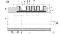
- FIG. 1 is a partial cross-sectional view showing the configuration of a semiconductor device according to a first embodiment
- FIG. 1 is a plan view showing a configuration of a semiconductor device according to Embodiment 1
- FIG. 10 is a partial cross-sectional view showing the configuration of a semiconductor device according to Modification 1 of Embodiment 1
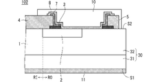
- FIG. 12 is a partial cross-sectional view showing the configuration of a semiconductor device according to Modification 2 of Embodiment 1
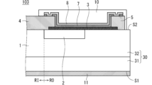
- FIG. 11 is a partial cross-sectional view showing the configuration of a semiconductor device according to Modification 3 of Embodiment 1
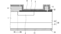
- FIG. 11 is a partial cross-sectional view showing the configuration of a semiconductor device according to Modification 3 of Embodiment 1; 4 is a partial cross-sectional view showing a manufacturing process of the semiconductor device according to Embodiment 1; FIG. 4 is a partial cross-sectional view showing a manufacturing process of the semiconductor device according to Embodiment 1; FIG. 4 is a partial cross-sectional view showing a manufacturing process of the semiconductor device according to Embodiment 1; FIG. 4 is a partial cross-sectional view showing a manufacturing process of the semiconductor device according to Embodiment 1; FIG. FIG. 11 is a partial cross-sectional view showing the configuration of a semiconductor device according to a second embodiment; FIG.
- FIG. 10 is a plan view showing the configuration of a semiconductor device according to a second embodiment
- FIG. 11 is a partial cross-sectional view showing the configuration of a unit cell of a semiconductor device according to a second embodiment
- FIG. 11 is a plan view showing the configuration of a semiconductor device according to Modification 1 of Embodiment 2
- FIG. 12 is a partial cross-sectional view showing the configuration of a semiconductor device according to Modification 2 of Embodiment 2
- FIG. 11 is a plan view showing the configuration of a semiconductor device according to Modification 2 of Embodiment 2
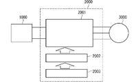
- FIG. 9 is a block diagram showing the configuration of a power conversion system to which a power conversion device according to Embodiment 3 is applied;
- the "active region” of the semiconductor device is the region through which the main current flows when the semiconductor device is in the ON state
- the "termination region” of the semiconductor device is the region surrounding the active region.
- the “outside” of the semiconductor device means the direction from the central portion to the outer peripheral portion of the semiconductor device
- the “inside” of the semiconductor device means the direction opposite to the "outside”.
- the conductivity type of the impurity the description will be made by assuming that the “first conductivity type” is n-type and the “second conductivity type” is p-type.
- the “second conductivity type” may be n-type.
- MOS Metal-Oxide-Semiconductor
- MOS transistors materials for gate insulating films and gate electrodes have been improved from the viewpoint of recent integration and improvements in manufacturing processes.
- MOS transistors polycrystalline silicon has been adopted as the material of the gate electrode instead of metal, mainly from the viewpoint of forming the source/drain in a self-aligned manner.
- a material with a high dielectric constant is used for the gate insulating film, but the material is not necessarily limited to oxide.
- MOS is not necessarily limited to the stacked structure of metal-oxide-semiconductor, and the same applies in this specification.
- MOS is defined not only as an abbreviation for Metal-Oxide-Semiconductor, but also broadly including a laminated structure of conductor-insulator-semiconductor.
- FIG. 1 is a partial cross-sectional view of a Schottky barrier diode (SBD) 100, which is a semiconductor device according to Embodiment 1.
- FIG. FIG. 2 is a plan view of the SBD 100, and FIG. 1 corresponds to a cross-sectional view taken along line AA in FIG.
- the left part of FIG. 1 is the active region through which the main current flows when the SBD 100 is on, and the right part of FIG.
- the region corresponding to the active region will be referred to as “inner region RI”
- the region corresponding to the termination region will be referred to as "outer region RO”.
- the SBD 100 is formed using an epitaxial substrate 30 composed of a single crystal substrate 31 and an epitaxial layer 32 formed thereon.
- Single crystal substrate 31 is a semiconductor substrate made of n-type (first conductivity type) silicon carbide (SiC), and epitaxial layer 32 is a semiconductor layer made of SiC epitaxially grown on single crystal substrate 31 . That is, the SBD 100 is a SiC-SBD.
- an epitaxial substrate 30 having a 4H polytype is used.
- the upper side of the epitaxial substrate 30 in FIG. 1 is defined as the "front side”, and the lower side is defined as the “back side”. ”.
- the back surface S1 of the epitaxial substrate 30 is also the main surface of the single crystal substrate 31, this is sometimes referred to as "the front surface S2 of the single crystal substrate 31".
- the surface S2 of the epitaxial substrate 30 is also the main surface of the epitaxial layer 32, this is sometimes referred to as "the surface S2 of the epitaxial layer 32".
- a p-type (second conductivity type) termination well region 2 is selectively formed in the surface layer portion on the front side of the epitaxial layer 32 in the termination region.
- the termination well region 2 is a frame-shaped (ring-shaped) region surrounding the active region in plan view, and functions as a so-called guard ring. Further, as shown in FIG. 1, the inner end (also referred to as the “inner peripheral end”) of the termination well region 2 is defined as the boundary between the inner region RI, which is the active region, and the outer region RO, which is the termination region. be done.
- the n-type region of the epitaxial layer 32 excluding the termination well region 2 is the drift layer 1 through which current flows due to drift.
- the impurity concentration of drift layer 1 is lower than that of single crystal substrate 31 . Therefore, single crystal substrate 31 has a lower resistivity than drift layer 1 .
- the impurity concentration of the drift layer 1 is set to 1 ⁇ 10 14 /cm 3 or more and 1 ⁇ 10 17 /cm 3 or less.
- the termination well region 2 may include multiple regions with different impurity concentrations. Also, the number of termination well regions 2 is not limited to one. For example, a plurality of termination well regions 2 spaced apart from each other and arranged in a nested manner may be provided in outer region RO. In other words, the terminal well region 2 may be divided into a plurality of parts.
- a field insulating film 3 , a surface electrode 4 , a peripheral electrode 5 , a moisture-resistant insulating film 7 , a semi-insulating film 8 and a surface protective film 10 are provided on the surface S 2 of the epitaxial substrate 30 .
- a back surface electrode 11 is provided on the back surface S ⁇ b>1 of the epitaxial substrate 30 . Note that the plan view of FIG. 2 shows only the epitaxial substrate 30 and the surface electrode 4, and the illustration of other elements is omitted.
- the field insulating film 3 partially covers the termination well region 2 and extends to the outside of the termination well region 2 beyond the outer edge of the termination well region 2 (also referred to as the "peripheral edge"). However, field insulating film 3 does not reach the outer peripheral edge of epitaxial substrate 30 , and surface S ⁇ b>2 of epitaxial substrate 30 is exposed outside field insulating film 3 . In the central portion of field insulating film 3, an opening is formed to expose surface S2 of the active region of epitaxial substrate 30. As shown in FIG.
- the surface electrode 4 is formed across the inner region RI and the outer region RO, and is connected to at least part of the surface S2 of the epitaxial substrate 30.
- the surface electrode 4 is provided over the entire inner region RI and is connected to the termination well region 2 in the outer region RO.
- the terminal well region 2 is connected to the outer peripheral portion of the surface electrode 4 and extends beyond the outer peripheral edge of the surface electrode 4 . Further, the outer peripheral edge of the surface electrode 4 rides on the inner peripheral edge of the field insulating film 3 .
- the material of the surface electrode 4 may be any metal that forms a Schottky junction with the drift layer 1, which is an n-type SiC semiconductor. Gold), W (tungsten), or the like can be used. Further, the surface electrode 4 is formed by laminating a metal such as Al (aluminum), Cu (copper), Mo or Ni, or an Al alloy such as Al—Si on any of the above materials. It may have a laminated structure.
- the peripheral electrode 5 is provided outside the termination well region 2 and spaced apart from the termination well region 2 and is connected to at least part of the surface S2 of the outer region RO of the epitaxial substrate 30 .
- the inner peripheral edge of the outer peripheral electrode 5 rides on the outer peripheral edge of the field insulating film 3 .
- the material of the peripheral electrode 5 may be any metal of Ti (titanium), Mo (molybdenum), Ni (nickel), Au (gold), W (tungsten), Al (aluminum), Cu (copper), or Al- Al alloys such as Si can be used. Further, the peripheral electrode 5 may have a laminated structure made of two or more of these materials.
- the moisture-resistant insulating film 7 is provided on at least part of the field insulating film 3 in the outer region RO.
- the inner peripheral end of the moisture-resistant insulating film 7 runs over the outer peripheral end of the surface electrode 4
- the outer peripheral end of the moisture-resistant insulating film 7 runs over the inner peripheral end of the outer peripheral electrode 5 . Therefore, the outer peripheral end face of the surface electrode 4 and the inner peripheral end face of the outer peripheral electrode 5 are covered with the moisture-resistant insulating film 7 .
- the moisture-resistant insulating film 7 does not entirely cover the surface electrode 4 and the outer peripheral electrode 5 , and portions other than the outer peripheral portion of the surface electrode 4 and portions other than the inner peripheral portion of the outer peripheral electrode 5 are separated from the moisture-resistant insulating film 7 . Exposed.
- an insulating film having high moisture resistance such as SiN, SiON, or SiOC is used as a material for the moisture-resistant insulating film 7, and an insulating film having high moisture resistance such as SiN, SiON, or SiOC is used.
- SiN is used as the material of the moisture-resistant insulating film 7, and its resistivity is 1 ⁇ 10 12 ⁇ cm or more.
- the film thickness of this SiN is 100 nm or more and 2000 nm or less, preferably 300 nm or more and 1500 nm or less, more preferably 500 nm or more and 1000 nm or less, for example, 500 nm.
- the semi-insulating film 8 is formed of a semi-insulating (conductive with relatively high resistivity) film and provided so as to cover the moisture-resistant insulating film 7 .
- the semi-insulating film 8 is connected to the surface electrode 4 exposed from the moisture-resistant insulating film 7 in the area inside the moisture-resistant insulating film 7, and exposed from the moisture-resistant insulating film 7 in the area outside the moisture-resistant insulating film 7. connected to the outer peripheral electrode 5.
- SInSiN Semi-Insulated SiN
- SIPOS Semi-Insulated Polycrystalline Silicon
- the semi-insulating film 8 only needs to have semi-insulating properties in the lower layer portions that are in contact with the surface electrode 4 and the peripheral electrode 5 . Therefore, the semi-insulating film 8 may have a laminated structure in which, for example, a highly moisture-resistant SiN film is laminated on an anti-insulating material.
- the surface protective film 10 is formed on the semi-insulating film 8 and covers the outer peripheral edge of the surface electrode 4 and the outer peripheral electrode 5 .
- the material of the surface protective film 10 is preferably an insulating resin material such as polyimide, polybenzoxal, etc., which can relax stress.
- the surface protection film 10 may be omitted.
- the moisture-resistant insulating film 7, the semi-insulating film 8 and the surface protective film 10 are provided with openings for exposing a region where dicing of the epitaxial substrate 30 is performed.
- FIG. 1 shows a cross section (a cross section along line AA in FIG. 2) of the end portion of the SBD 100 according to the first embodiment. It is preferable to have a cross-sectional structure of That is, the moisture-resistant insulating film 7 preferably covers the entire circumference of the outer peripheral end of the surface electrode 4 and the entire circumference of the inner peripheral end of the outer peripheral electrode 5 in plan view.
- the material of the epitaxial substrate 30 is SiC.
- SiC semiconductors have a wider bandgap than Si semiconductors. Compared to Si semiconductor devices, SiC semiconductor devices have excellent withstand voltage, high allowable current density, and high heat resistance, so they can operate at high temperatures. be.
- the material of the epitaxial substrate 30 is not limited to SiC, and may be Si or another wide bandgap semiconductor such as gallium nitride (GaN).
- the semiconductor device according to the present embodiment may be a diode other than the SBD, such as a pn junction diode or a Junction Barrier Schottky (JBS) diode.
- a diode other than the SBD such as a pn junction diode or a Junction Barrier Schottky (JBS) diode.
- JBS Junction Barrier Schottky
- FIG. 3 is a cross-sectional view showing the configuration of SBD 101 according to Modification 1 of Embodiment 1.
- the termination well region 2 is divided into multiple parts.
- Field insulating film 3 has openings on each of the plurality of termination well regions 2 .
- a plurality of auxiliary electrodes 6 are formed on the field insulating film 3 so as to be connected to each of the plurality of divided termination well regions 2 .
- Auxiliary electrodes 6 are connected to corresponding termination well regions 2 through openings in field insulating film 3 . That is, the plurality of auxiliary electrodes 6 are connected to the plurality of termination well regions 2 and run over the field insulating film 3 .
- the moisture-resistant insulating film 7 is provided so as to cover the plurality of auxiliary electrodes 6 and has openings on each of the plurality of auxiliary electrodes 6 .
- a semi-insulating film 8 formed on the moisture-resistant insulating film 7 is connected to a plurality of auxiliary electrodes 6 through openings in the moisture-resistant insulating film 7 .
- the material of the auxiliary electrode 6 is a metal containing any one of Ti (titanium), Mo (molybdenum), Ni (nickel), Au (gold), W (tungsten), Al (aluminum), Cu (copper), or Al An Al alloy such as Si (silicon) or the like can be used.
- the auxiliary electrode 6 may be a laminated structure made of two or more of these materials.
- FIG. 4 is a cross-sectional view showing the configuration of SBD 102 according to Modification 2 of Embodiment 1. As shown in FIG. In SBD 102 of FIG. 4 , field insulating film 3 and moisture-resistant insulating film 7 have openings exposing surface S 2 of epitaxial substrate 30 including termination well region 2 . Semi-insulating film 8 is connected to epitaxial substrate 30 including termination well region 2 through its opening.
- FIG. 5 is a cross-sectional view showing the configuration of SBD 103 according to Modification 3 of Embodiment 1.
- the moisture-resistant insulating film 7 has an opening at a position different from its edge, and the semi-insulating film 8 is connected to the surface electrode 4 and the peripheral electrode 5 through the opening.
- the moisture-resistant insulating film 7 has an opening for connecting the semi-insulating film 8 to the surface electrode 4 and an opening for connecting the semi-insulating film 8 to the outer electrode 5 between the inner peripheral end and the outer peripheral end of the moisture-resistant insulating film 7 .
- An opening is provided for
- the outer peripheral edge of the moisture-resistant insulating film 7 may be located outside the outer peripheral electrode 5 . That is, like the SBD 104 shown in FIG. 6, the moisture-resistant insulating film 7 may cover not only the inner peripheral end of the outer peripheral electrode 5 but also the outer peripheral end.
- the semi-insulating film 8 may also extend onto the moisture-resistant insulating film 7 outside the outer peripheral electrode 5 .
- the SBD 100 When the SBD 100 is in the off state, a large electric field is applied to the surface of the active region of the drift layer 1 and the vicinity of the pn junction interface between the drift layer 1 and the termination well region 2 .
- the voltage to the backside electrode 11 when this electric field reaches the critical electric field and avalanche breakdown occurs is defined as the maximum voltage (avalanche voltage).
- the rated voltage is determined so that the SBD 100 is used within a voltage range in which avalanche breakdown does not occur.
- the direction toward single crystal substrate 31 (downward direction) and the outer peripheral direction of drift layer 1 ( to the right) and the depletion layer spreads.
- a depletion layer also spreads into the termination well region 2 from the pn junction interface between the drift layer 1 and the termination well region 2 , and the degree of spread depends largely on the concentration of the termination well region 2 . That is, when the concentration of the termination well region 2 increases, the spread of the depletion layer is suppressed in the termination well region 2, and the tip position of the depletion layer inside the termination well region 2 becomes the boundary between the termination well region 2 and the drift layer 1. position close to
- the surface protective film 10 is composed of polyimide or the like
- the surface protective film 10 contains a large amount of moisture under high humidity.
- the voltage applied to the SBD 100 in the OFF state causes the surface electrode 4 to act as a cathode and the peripheral electrode 5 to act as an anode.
- the surface protective film 10 is not formed, a large amount of moisture permeates the sealing gel and reaches the SBD 100, and similarly the surface electrode 4 acts as a cathode and the peripheral electrode 5 acts as an anode.
- the oxygen reduction reaction represented by the following chemical formula (1) and the hydrogen generation reaction represented by the following chemical formula (2) occur with respect to the moisture.
- the concentration of hydroxide ions increases near the surface electrode 4 .
- Hydroxide ions chemically react with the surface electrode 4 .
- the chemical reaction described above may turn the aluminum into aluminum hydroxide.
- aluminum hydroxide may change to aluminum oxide depending on the ambient temperature and pH.
- the aluminum melts as Al 3+ and reacts with surrounding moisture to form aluminum hydroxide or aluminum oxide.
- These aluminum hydroxides or aluminum oxides are deposited on the surfaces of the surface electrode 4 and the peripheral electrode 5 as insulators. This deposition cracks or pushes up the films on the surface electrode 4 and the outer peripheral electrode 5 to separate them, and when the separation progresses and a cavity is formed above the field insulating film 3, water is trapped in the cavity. enter. Moisture that has entered the cavity may cause excessive leakage current, air discharge in the cavity, and the like, and may cause the SBD to break down. Further, when volume expansion occurs due to deposition of an insulator, stress is applied to the field insulating film 3 and the epitaxial substrate 30 under the surface electrode 4 and the outer peripheral electrode 5, causing physical destruction of the SBD 100 and element destruction. can be the cause.
- the above deposition reaction of aluminum hydroxide or aluminum oxide is accelerated by electric field strength.
- the outer peripheral edge of the surface electrode 4 and the inner peripheral edge of the outer peripheral electrode 5 are likely to have a high electric field, and when the epitaxial substrate 30 is made of silicon carbide, the drift layer 1 has a high concentration, so the electric field strength is further increased. As a result, the precipitation reaction of aluminum hydroxide or aluminum oxide is accelerated.
- the semi-insulating film 8 is connected to the outer peripheral end of the surface electrode 4 and the inner peripheral end of the outer peripheral electrode 5, and moisture in the surface protective film 10 passes through the semi-insulating film 8.
- the end portions of the surface electrode 4 and the peripheral electrode 5 are reached, electrons are exchanged between the surface electrode 4 and the peripheral electrode 5 through the semi-insulating film 8, and the precipitation reaction of aluminum hydroxide or aluminum oxide further proceeds. accelerated.
- a potential gradient is likely to occur around the outer peripheral edge of the surface electrode 4 and the inner peripheral edge of the outer peripheral electrode 5, accelerating the deposition reaction of aluminum hydroxide or aluminum oxide due to the electric field intensity. may also occur.
- the moisture-resistant insulating film 7 covers the outer end face of the surface electrode 4 and the inner end face of the outer peripheral electrode 5 .
- deposition of aluminum hydroxide or aluminum oxide around the outer peripheral edge of the surface electrode 4 and the inner peripheral edge of the outer peripheral electrode 5 can be suppressed.
- the semi-insulating film 8 is connected to the surface electrode 4 and the peripheral electrode 5 exposed from the moisture-resistant insulating film 7, so that a gentle potential gradient is generated from the surface electrode 4 to the peripheral electrode 5. It is formed. Therefore, it is possible to suppress the occurrence of excessive electric field concentration around the termination well region 2 .
- the inner peripheral end and the outer peripheral end of the auxiliary electrode 6 where the electric field tends to concentrate are covered with the moisture-resistant insulating film 7 . Therefore, it is difficult for moisture to reach the inner peripheral edge and the outer peripheral edge of the auxiliary electrode 6, and deposition of aluminum hydroxide or aluminum oxide can be suppressed. Further, since the semi-insulating film 8 is connected to the auxiliary electrode 6 through the opening of the moisture-resistant insulating film 7, the potential of the plurality of terminal well regions 2 formed apart is fixed, and the peripheral region of the terminal well region 2 is fixed. Electric field concentration can be relaxed more effectively.
- the semi-insulating film 8 is connected to the epitaxial substrate 30 including the termination well region 2.
- the semi-insulating film 8 is connected to the surface electrode 4 and the outer peripheral electrode 5 through openings provided at positions different from the edges of the moisture-resistant insulating film 7 .
- edge portions such as an insulating film are located on the surface of the surface electrode 4 and the peripheral electrode 5
- water is likely to remain due to the structure, and aluminum hydroxide or aluminum oxide is deposited on the surface of the surface electrode 4 and the peripheral electrode 5. Reaction is likely to occur.
- edges of the semi-insulating film 8 are located on the surfaces of the surface electrode 4 and the peripheral electrode 5, electrons are exchanged with the surface electrode 4 and the peripheral electrode 5 through the semi-insulating film 8, so that the surface electrode 4 and the deposition reaction of aluminum hydroxide or aluminum oxide on the surface of the peripheral electrode 5 is accelerated.
- the edges of the semi-insulating film 8 are separated from the surfaces of the surface electrode 4 and the peripheral electrode 5, so that precipitation reaction of aluminum hydroxide or aluminum oxide on the surfaces of the surface electrode 4 and the peripheral electrode 5 is suppressed. can do.
- the moisture-resistant insulating film 7 covers both the inner end face and the outer end face of the outer peripheral electrode 5 . Thereby, the deposition reaction of aluminum hydroxide or aluminum oxide can be suppressed on the entire surface of the peripheral electrode 5 .
- the moisture-resistant insulating film 7 and the semi-insulating film 8 run over the field insulating film 3 in the region outside the outer peripheral electrode 5 . Therefore, the region of the epitaxial substrate 30 that can become the anode outside the peripheral electrode 5 is covered with the field insulating film 3 and the moisture-resistant insulating film 7, so that deposition of an insulator due to anodization of the epitaxial substrate 30 can be suppressed. .
- a low-resistance single-crystal substrate 31 containing n-type impurities at a relatively high concentration (n + ) is prepared.
- the single crystal substrate 31 is assumed to be a SiC substrate having a 4H polytype and an off angle of 4 degrees or 8 degrees.
- SiC is epitaxially grown on the single crystal substrate 31 to form an epitaxial layer 32 of n-type with an impurity concentration of 1 ⁇ 10 14 /cm 3 or more and 1 ⁇ 10 17 /cm 3 or less.
- epitaxial substrate 30 consisting of single crystal substrate 31 and epitaxial layer 32 is obtained.
- a resist mask having a predetermined pattern is formed on the epitaxial layer 32 by a photolithography process, and a p-type impurity (acceptor) such as Al or B (boron) is implanted using the resist mask as an implantation mask.
- a p-type termination well region 2 is formed in the upper layer of the epitaxial layer 32 by ion implantation.
- the dose amount of the termination well region 2 is preferably 0.5 ⁇ 10 13 /cm 2 or more and 5 ⁇ 10 13 /cm 2 or less, for example, 1.0 ⁇ 10 13 /cm 2 .
- the ion implantation energy for forming the termination well region 2 is, for example, 100 keV or more and 700 keV or less in the case of Al.
- the impurity concentration converted from the dose amount [cm ⁇ 2 ] is 1 ⁇ 10 17 /cm 3 or more and 1 ⁇ 10 19 /cm 3 or less.
- a resist mask is patterned so that a plurality of loop-shaped p-type impurity regions are formed in a nested manner.
- An additional termination well region 2 can be formed.
- the termination well region 2 comprising a plurality of regions with different impurity concentrations can be formed.
- annealing is performed in an inert gas atmosphere such as argon (Ar) gas at a temperature of 1300° C. or higher and 1900° C. or lower for 30 seconds or more and 1 hour or less. This annealing activates the impurities added by the ion implantation.
- argon (Ar) gas such as argon (Ar) gas at a temperature of 1300° C. or higher and 1900° C. or lower for 30 seconds or more and 1 hour or less.
- a 1 ⁇ m-thick SiO 2 film to be the field insulating film 3 is deposited on the surface S2 of the epitaxial substrate 30 by, eg, CVD.
- a resist mask having a predetermined pattern is formed on the SiO 2 film by a photolithography process, and the SiO 2 is etched using the resist mask as an etching mask, thereby forming the field insulating film 3 .
- the SiO 2 film in the region where the epitaxial substrate 30 contacts with the surface electrode 4 and the peripheral electrode 5 is removed.
- the SiO 2 film in the region where the auxiliary electrode 6 and the epitaxial substrate 30 are in contact is also removed.
- a Ti film with a thickness of 100 nm and an Al film with a thickness of 3 ⁇ m, for example, are formed in this order on the epitaxial layer 32 by, for example, a sputtering method.
- a resist mask having a predetermined pattern is formed on the Al film by a photolithography process, and RIE (Reactive Ion Etching) of the Al film is performed using the resist mask as an etching mask, thereby removing the surface electrode 4 and the outer periphery.
- An electrode 5 is formed.
- the auxiliary electrode 6 can be formed in this step.
- a SiN film to be the moisture-resistant insulating film 7 is formed by plasma CVD, for example.
- the SiN film can be obtained.
- the resistivity is set to 1 ⁇ 10 12 ⁇ cm or more.
- the resistivity of the SiN film has a correlation with the refractive index, and the refractive index is generally 2.2 or less.
- a resist mask having a predetermined pattern is formed on the SiN film by a photolithography process, and the SiN film is etched using the resist mask as an etching mask to form the moisture-resistant insulating film 7 .
- the SiN film in the region connecting the semi-insulating film 8 and the surface electrode 4 and the region connecting the semi-insulating film 8 and the peripheral electrode 5 are removed.
- the SiN film in the region connecting the semi-insulating film 8 and the auxiliary electrode 6 is also removed.
- the SiN film to be the moisture-resistant insulating film 7 can also be formed by thermal CVD, in which case the composition is stoichiometrically closer to Si 3 N 4 .
- the refractive index of Si 3 N 4 is about 2.0 or more and 2.1 or less.
- the SiN film formed by thermal CVD is superior in moisture resistance and insulating properties, but the film formation temperature is much higher than in plasma CVD. Therefore, when a material containing Al is used for the surface electrode 4 or the like, the film formation temperature exceeds the melting point of Al, and the SiN film cannot be formed by thermal CVD. If the material of the surface electrode 4 is, for example, Cu or the like and does not contain Al, it is possible to form a SiN film by thermal CVD.
- a SInSiN film to be the semi-insulating film 8 is formed by plasma CVD, for example.
- the resistivity of the SInSiN film is set to less than 1 ⁇ 10 12 ⁇ cm by adjusting the flow rate of silane gas (SiH 4 ) or the like as a raw material.
- the resistivity of the SInSiN film has a correlation with the refractive index, and although the refractive index generally exceeds 2.2, it may become 2.2 or less due to changes in the bonding state in the film depending on the manufacturing method or the like.
- a resist mask having a predetermined pattern is formed on the SInSiN film by a photolithography process, and the SInSiN film is etched using the resist mask as an etching mask, thereby forming a semi-insulating film 8 .
- the SInSiN film in the regions where wire bonding, dicing, etc. are performed is removed.
- the semi-insulating film 8 may have a laminated structure by forming a SiN film with high moisture resistance and insulation on the SInSiN film.
- the SiN film and the SInSiN film can be etched in the same process. Therefore, when the moisture-resistant insulating film 7 and the semi-insulating film 8 are formed of the SiN film and the SInSiN film, the patterning of the moisture-resistant insulating film 7 and the semi-insulating film 8 may be performed in the following procedure.
- a SiN film to be the moisture-resistant insulating film 7 is formed so as to cover the surface electrode 4, the peripheral electrode 5 and the field insulating film 3, and as shown in FIG.
- a first etching step is performed to remove the SiN film in the region connecting the semi-insulating film 8 and the peripheral electrode 5 and form an opening in the moisture-resistant insulating film 7 .
- the SiN film is left in the regions where wire bonding, dicing, and the like are performed.
- a SInSiN film that will become the semi-insulating film 8 is formed so as to cover the moisture-resistant insulating film 7 .
- etching both the SiN film (moisture-resistant insulating film 7) and the semi-insulating film 8 (SInSiN film) using the same etching mask as shown in FIG.
- a second etching process is performed to form an opening penetrating through the moisture-resistant insulating film 7 and the semi-insulating film 8 .
- a part of the surface electrode 4 is exposed in the opening of the wire bonding area, and the field insulating film 3 is exposed in the dicing area.
- the moisture-resistant insulating film 7 and the semi-insulating film 8 By patterning the moisture-resistant insulating film 7 and the semi-insulating film 8 in such a procedure, the number of times of overetching of the surface electrode 4, the outer peripheral electrode 5, and the field insulating film 3 can be reduced, and the surface electrode 4 and the outer peripheral film 3 are etched. Damage to the electrode 5 and the field insulating film 3 can be suppressed. By suppressing deterioration due to overetching of the surfaces of the surface electrode 4 and the outer peripheral electrode 5, an effect of suppressing a state in which deposition of an insulator is likely to occur can be expected.
- the field insulating film 3 is also provided in a region outside the outer peripheral electrode 5, and damage to the epitaxial substrate 30 during etching of the SiN film and the SInSiN film may occur. is suppressed.
- the SiN film and the SiO 2 film can be etched in the same process. Therefore, when forming the SBD 102 of FIG. 4, as shown in FIG. 10, by etching for patterning the SiN film of the moisture-resistant insulating film 7, the semi-insulating film 8 and the termination well are formed on the field insulating film 3 made of SiO 2 film. An opening for connecting epitaxial substrate 30 including region 2 may be formed. Also, this etching may be performed in the first etching step described above. That is, in the first etching step, an opening may be further formed through both the moisture-resistant insulating film 7 and the field insulating film 3 to expose a portion of the epitaxial layer 32 .
- the moisture-resistant insulating film 7 and the semi-insulating film 8 for example, photosensitive polyimide is applied to the surface electrode 4, the peripheral electrode 5, the field insulating film 3, the moisture-resistant insulating film 7, the semi-insulating film 8, and the surface S2 of the epitaxial substrate 30. , and a surface protective film 10 having a predetermined pattern is formed by a photolithography process.
- a sealing gel having a low elastic modulus such as silicone gel
- the back surface electrode 11 is formed on the back surface S1 of the epitaxial substrate 30 by, for example, sputtering, thereby obtaining the structure of the SBD 100 shown in FIG.
- the formation of the back electrode 11 may be performed before or after the step of forming the surface electrode 4 and the peripheral electrode 5 .
- a metal or the like containing one or more of Ti, Ni, Al, Cu, and Au can be used as the material of the back electrode 11.
- the thickness of the back electrode 11 is preferably 50 nm or more and 2 ⁇ m or less.
- the back electrode 11 may be formed of a two-layer film (Ti/Au) of Ti and Au each having a thickness of 1 ⁇ m or less.
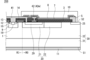
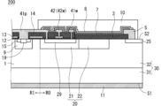
- FIG. 11 is a partial cross-sectional view showing the configuration of a MOSFET 200, which is a semiconductor device according to the second embodiment.
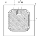
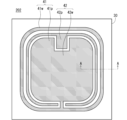
- FIG. 12 is a plan view of the MOSFET 200
- FIG. 11 corresponds to a cross-sectional view taken along line BB in FIG.
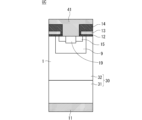
- FIG. 13 is a cross-sectional view showing the configuration of a unit cell UC, which is the minimum unit structure of MOSFETs formed in the inner region RI, which is an active region.
- a plurality of unit cells UC shown in FIG. 13 are arranged in the inner region RI of the MOSFET 200 (the outermost unit cell UC is shown in the left end portion of FIG. 11).
- 11 to 13 elements having the same functions as the elements of the SBD 100 according to the first embodiment shown in FIGS. 1 and 2 are denoted by the same reference numerals. Explanations overlapping with those of the first embodiment will be omitted.
- the MOSFET 200 is formed using an epitaxial substrate 30 composed of a single crystal substrate 31 and an epitaxial layer 32 formed thereon.
- Single crystal substrate 31 is a semiconductor substrate made of n-type (first conductivity type) silicon carbide (SiC)
- epitaxial layer 32 is a semiconductor layer made of SiC epitaxially grown on single crystal substrate 31 .
- MOSFET 200 is a SiC-MOSFET.
- an epitaxial substrate 30 having a 4H polytype is used.
- a p-type (second conductivity type) element well region 9 is selectively formed in the surface layer portion on the front side of the epitaxial layer 32 in the active region.
- an n-type source region 15 and a p-type contact region 19 having an impurity peak concentration higher than that of the element well region 9 are selectively formed in the surface layer of the element well region 9 .
- a p-type termination well region 20 is selectively formed in the surface layer portion on the front side of the epitaxial layer 32 in the termination region so as to surround the active region.
- the termination well region 20 extends outward from the high-concentration region 21 so as to surround the high-concentration region 21 contacting the boundary between the inner region RI and the outer region RO, and the high-concentration region 21 . and a low concentration region 22 having a low peak concentration.
- a termination contact region 29 having an impurity peak concentration higher than that of the high-concentration region 21 is provided in the surface layer portion of the high-concentration region 21 .
- the conductivity type of the termination contact region 29 may be n-type.
- an n-type outer peripheral contact region 25 is formed in the surface layer portion of the outer peripheral portion of the epitaxial layer 32 .
- the conductivity type of the outer peripheral contact region 25 may be p-type.
- the n-type region of the epitaxial layer 32 excluding the above impurity regions is the drift layer 1 through which current flows due to drift. .
- the impurity concentration of drift layer 1 is lower than that of single crystal substrate 31 . Therefore, single crystal substrate 31 has a lower resistivity than drift layer 1 .
- the impurity concentration of the drift layer 1 is set to 1 ⁇ 10 14 /cm 3 or more and 1 ⁇ 10 17 /cm 3 or less.
- the termination well region 20 is a frame-shaped (ring-shaped) region surrounding the active region in plan view, and functions as a so-called guard ring. Further, as shown in FIG. 11, with the inner (inner peripheral side) edge of the termination well region 20 as a boundary, the inner region RI, which is the active region, is located inside, and the outer region RO, which is the termination region, is located outside. is defined as
- gate insulating film 12 is formed so as to straddle source region 15, device well region 9 and drift layer 1, and gate electrode 13 is formed thereon. ing.
- a surface layer portion of the device well region 9 covered with the gate insulating film 12 and the gate electrode 13, that is, a portion of the device well region 9 between the source region 15 and the drift layer 1 has an inversion channel when the MOSFET 200 is turned on. It is the channel region to be formed.
- the gate electrode 13 is covered with an interlayer insulating film 14, and a source electrode 41, which is a surface electrode, is formed on the interlayer insulating film 14. Therefore, the interlayer insulating film 14 electrically insulates between the gate insulating film 12 and the gate electrode 13 . As shown in FIG. 12, the source electrode 41 is provided over the entire inner region RI.
- the source electrode 41 is connected to the source region 15 and contact region 19 through contact holes formed in the interlayer insulating film 14 .
- Source electrode 41 and contact region 19 form an ohmic contact.
- a back surface electrode 11 functioning as a drain electrode is formed on the back surface S1 of the epitaxial substrate 30 .
- gate electrode 13, interlayer insulating film 14, and source electrode 41 extends to outer region RO beyond the boundary between inner region RI and outer region RO. ing.
- the source electrode 41 drawn out to the outer region RO is connected to the termination contact region 29 in the termination well region 20 through a contact hole formed in the interlayer insulating film 14 so as to form an ohmic contact or a Schottky contact.
- the gate electrode 13 drawn out to the outer region RO is arranged on the high-concentration region 21 of the termination well region 20 via the gate insulating film 12, and extends like the high-concentration region 21 in plan view in a frame shape. exist.
- a gate wiring electrode 42 formed on the interlayer insulating film 14 is connected to the gate electrode 13 drawn out to the outer region RO through an opening provided in the interlayer insulating film 14 .
- the gate wiring electrode 42 is a control wiring electrode for receiving a gate signal (control signal) for controlling an electrical path between the source electrode 41 and the back surface electrode 11 which is a drain electrode. It is spaced apart and electrically insulated from the source electrode 41 .
- the gate wiring electrode 42 includes a gate wiring 42w provided so as to surround the source electrode 41 and a gate pad 42p for wire bonding.
- the source electrode 41 is rectangular in plan view
- the gate pad 42p is provided so as to enter a recess formed on one side of the rectangular source electrode 41 .
- the gate wiring electrode 42 shown in FIG. 11 corresponds to the gate wiring 42w. Note that the plan view of FIG. 12 shows only the epitaxial substrate 30, the source electrode 41 and the gate wiring electrode 42, and the illustration of other elements is omitted.
- the gate wiring 42w and the gate pad 42p are directly connected in FIG. 12, the gate wiring 42w and the gate pad 42p are separated from each other and electrically connected through the gate electrode 13 under the interlayer insulating film 14. may be configured.
- Field insulating film 3 is provided on surface S2 of outer region RO of epitaxial substrate 30, covers part of high-concentration region 21 and the entirety of low-concentration region 22, and extends to the vicinity of the edge of epitaxial substrate 30. do. Field insulating film 3 is not provided in inner region RI. That is, the field insulating film 3 is provided with an opening that encloses the inner region RI.
- the field insulating film 3 is connected to the side surface of the interlayer insulating film 14 in FIG.
- the field insulating film 3 and the interlayer insulating film 14 may be an integral film formed at the same time.
- the peripheral electrode 5 is provided on the surface S ⁇ b>2 of the epitaxial substrate 30 apart from the termination well region 20 and connected to at least part of the surface of the peripheral contact region 25 .
- the inner peripheral edge of the outer peripheral electrode 5 rides on the outer peripheral edge of the field insulating film 3 .
- the moisture-resistant insulating film 7 is provided on at least part of the field insulating film 3 in the outer region RO, and covers the outer peripheral edge of the source electrode 41, the inner peripheral edge of the outer peripheral electrode 5, and the inner and outer peripheral edges of the gate wiring electrode 42. covering the The moisture-resistant insulating film 7 has openings on the source electrode 41 , the peripheral electrode 5 and the gate wiring electrode 42 . However, the opening on the gate wiring electrode 42 is provided on the gate pad 42p not shown in FIG.
- the semi-insulating film 8 is provided so as to cover the moisture-resistant insulating film 7 and is connected to the source electrode 41 and the peripheral electrode 5 exposed from the moisture-resistant insulating film 7 .
- Semi-insulating film 8 is not connected to gate pad 42p.
- the surface protective film 10 is provided so as to cover the outer peripheral edge of the source electrode 41 , the inner and outer peripheral edges of the gate wiring electrode 42 , and the outer peripheral electrode 5 . Openings are formed in the surface protective film 10 above the source electrode 41 and the gate pad 42p. Note that when the MOSFET 200 is used while being covered with a sealing gel having a low elastic modulus such as silicone gel, the surface protection film 10 may be omitted.
- the moisture-resistant insulating film 7, the semi-insulating film 8, and the surface protection film 10 are opened in the regions where wire bonding and the like are performed on the source electrode 41 and the gate pad 42p and the regions where dicing and the like are performed on the epitaxial substrate 30.
- FIG. 11 shows a cross section (a cross section along the line BB in FIG. 12) of the terminal portion of the MOSFET 200 according to the second embodiment. It is preferable to have a cross-sectional structure similar to that of FIG. 11 at all positions of the part.
- the moisture-resistant insulating film 7 covers the inner peripheral edge and the outer peripheral edge of the gate pad 42p at all positions where the gate pad 42p is arranged. That is, the moisture-resistant insulating film 7 covers the entire circumference of the outer peripheral edge of the source electrode 41, the entire circumference of the inner peripheral edge of the outer peripheral electrode 5, and the entire inner and outer peripheral edges of the gate wiring electrode 42 in plan view. preferably covered.
- the moisture-resistant insulating film 7 covers the entire circumference of the inner peripheral end and the outer peripheral end of the gate wiring 42w in plan view.
- epitaxial substrate 30 has been described as being made of SiC.
- SiC has a wider bandgap than Si, and a SiC semiconductor device using SiC has excellent withstand voltage, a high allowable current density, and high heat resistance compared to a Si semiconductor device using Si. Therefore, high temperature operation is also possible.
- the material of the epitaxial substrate 30 is not limited to SiC, and may be composed of other wide bandgap semiconductors such as gallium nitride (GaN). Silicon (Si), for example, may be used instead of the wide bandgap semiconductor.
- the semiconductor device may be a transistor other than a MOSFET, such as a JFET (Junction FET) or an IGBT (Insulated Gate Bipolar Transistor).
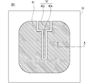
- FIG. 14 is a plan view showing the configuration of MOSFET 201 according to Modification 1 of Embodiment 2. As shown in FIG. In FIG. 14, only the source electrode 41 and the gate wiring electrode 42 are shown in the upper surface configuration of the MOSFET 201 for the sake of convenience. In the MOSFET 201 shown in FIG. 14, unlike the MOSFET 200 shown in FIG. 12, the gate wiring 42w does not surround the source electrode 41, but is provided so as to enter a recess deeply formed in one side of the rectangular source electrode 41 in plan view. .
- the moisture-resistant insulating film 7 covers the outer edge of the source electrode 41, the inner edge of the outer peripheral electrode 5, and the inner and outer peripheral edges of the gate wiring electrode 42. , and has openings on the source electrode 41 , the peripheral electrode 5 and the gate wiring electrode 42 .
- the moisture-resistant insulating film 7 completely covers the gate wiring 42w, and the opening above the gate wiring electrode 42 is provided at the gate pad 42p.
- the semi-insulating film 8 is provided so as to cover the moisture-resistant insulating film 7 and is connected to the source electrode 41 and the peripheral electrode 5 exposed from the moisture-resistant insulating film 7 . Also, the semi-insulating film 8 is not connected to the gate wiring electrode 42 .
- FIG. 15 is a partial cross-sectional view showing the configuration of MOSFET 202 according to Modification 2 of Embodiment 2
- FIG. 16 is a plan view showing the configuration of MOSFET 202. As shown in FIG. 16 corresponds to FIG. 15. FIG. In FIG. 16, only the source electrode 41 and the gate wiring electrode 42 of the upper surface configuration of the MOSFET 202 are shown for convenience.
- the source electrode 41 includes a rectangular source pad 41p in plan view, and a source wiring 41w which is a surface wiring formed to surround the gate wiring electrode 42 including the gate wiring 42w. .
- the gate wiring 42w is opened on the plane, and the source wiring 41w and the source pad 41p are directly connected at the opening of the gate wiring 42w. They may be separated and electrically connected by providing a conductive film other than the source electrode 41 , the gate wiring electrode 42 and the gate electrode 13 , or may be electrically connected via the termination contact region 29 . .
- the moisture-resistant insulating film 7 runs over the source electrode 41 , the gate wiring electrode 42 and the outer peripheral electrode 5 , and extends to the outer edge of the source pad 41 p , the inner and outer peripheral edges of the source wiring 41 w , and the inner and outer edges of the gate wiring electrode 42 . It covers the peripheral edge, the outer peripheral edge, and the inner peripheral edge of the outer peripheral electrode 5 .
- the moisture-resistant insulating film 7 preferably covers the entire circumference of the inner peripheral end and the outer peripheral end of the source wiring 41w in plan view.
- openings are formed in the moisture-resistant insulating film 7 above the source electrode 41 , the peripheral electrode 5 and the gate wiring electrode 42 .
- An opening on the source electrode 41 is provided on both the source wiring 41w and the source pad 41p.
- the opening on the gate wiring electrode 42 is provided on the gate pad 42p, but not on the gate wiring 42w, and the gate wiring 42w is completely covered with the moisture-resistant insulating film 7.
- the semi-insulating film 8 is provided so as to cover the moisture-resistant insulating film 7 and is connected to the source wiring 41w and the peripheral electrode 5 at the opening of the moisture-resistant insulating film 7 .
- Semi-insulating film 8 is not connected to source pad 41p and gate pad 42p.
- a first state is a state in which a positive voltage equal to or higher than the threshold is applied to the gate electrode 13 .
- This state is hereinafter referred to as the "on state".
- an inversion channel is formed in the channel region.
- the inversion channel serves as a path for electrons, which are carriers, to flow between the source region 15 and the drift layer 1 .
- the ON state when a high voltage is applied to the back electrode 11 with the source electrode 41 as a reference, current flows through the single crystal substrate 31 and the drift layer 1 .
- a voltage between the source electrode 41 and the back electrode 11 at this time is called an ON voltage, and a current flowing between the source electrode 41 and the back electrode 11 is called an ON current.
- the on-current flows only through the inner region RI where the channel exists and does not flow through the outer region RO.
- a second state is a state in which a voltage less than the threshold is applied to the gate electrode 13 .
- This state is hereinafter referred to as an "off state".
- the off state no inversion channel is formed in the channel region, so no on-current flows. Therefore, when a high voltage is applied between the source electrode 41 and the back electrode 11, this high voltage is maintained. At this time, since the voltage between the gate electrode 13 and the source electrode 41 is much smaller than the voltage between the source electrode 41 and the back electrode 11, the voltage between the gate electrode 13 and the back electrode 11 is also high. A voltage will be applied.
- a high voltage is applied between each of the gate wiring electrode 42 and the gate electrode 13 and the back surface electrode 11 also in the outer region RO. Electrical contact with the source electrode 41 is formed in the element well region 9 in the inner region RI, and electrical contact with the source electrode 41 is formed in the termination contact region 29 in the outer region RO. Therefore, application of a high electric field to the gate insulating film 12 and the interlayer insulating film 14 is prevented.
- the outer region RO in the OFF state operates similarly to the SBD 100 in the OFF state described in the first embodiment. That is, a high electric field is applied near the pn junction interface between the drift layer 1 and the termination well region 20 , and avalanche breakdown occurs when a voltage exceeding the critical electric field is applied to the back electrode 11 . Normally, the rated voltage is determined so that the MOSFET 200 is used within a range in which avalanche breakdown does not occur.
- drift layer 1 In the off state, from the pn junction interface between drift layer 1 and element well region 9 and termination well region 20 , a direction toward single crystal substrate 31 (downward) and an outer peripheral direction (rightward) of drift layer 1 .
- the depletion layer spreads.
- the MOSFET 200 is turned off under high humidity.
- the surface protective film 10 is made of polyimide or the like, it contains a large amount of water under high humidity.
- the voltage applied to the MOSFET 200 in the OFF state causes the source electrode 41 and the gate wiring electrode 42 to act as the cathode and the peripheral electrode 5 as the anode. works.
- the surface protective film 10 is not formed, a large amount of moisture permeates the sealing gel and reaches the MOSFET 200, and similarly the source electrode 41 and the gate wiring electrode 42 act as a cathode, and the peripheral electrode 5 acts as an anode.
- a voltage equal to or lower than that of the source electrode 41 is applied to the gate electrode 13, the relation that the gate wiring electrode 42 is the cathode and the source electrode 41 is the anode also holds.
- the oxygen reduction reaction and the hydrogen generation reaction described in the first embodiment occur.
- the concentration of hydroxide ions increases in the vicinity of the source electrode 41 and the gate wiring electrode 42 .
- Hydroxide ions chemically react with the source electrode 41 and the gate wiring electrode 42 .
- the source electrode 41 and the gate wiring electrode 42 are made of aluminum, the aluminum may become aluminum hydroxide due to the chemical reaction.
- aluminum hydroxide may change to aluminum oxide depending on the ambient temperature and pH.
- the aluminum melts as Al 3+ and reacts with surrounding moisture to form aluminum hydroxide or aluminum oxide.
- the above deposition reaction of aluminum hydroxide or aluminum oxide is accelerated by electric field strength.
- the outer peripheral edge of the gate wiring electrode 42 and the inner peripheral edge of the outer peripheral electrode 5 are likely to have a high electric field, and when the epitaxial substrate 30 is made of silicon carbide, the drift layer 1 has a high concentration, so the electric field strength is further increased. increases, accelerating the precipitation reaction of aluminum hydroxide or aluminum oxide.
- the voltage applied to the gate wiring electrode 42 also creates a high electric field at the outer peripheral edge of the source electrode 41 and the inner peripheral edge of the gate wiring electrode 42, accelerating the deposition reaction of aluminum hydroxide or aluminum oxide.
- the moisture flows through the semi-insulating film 8 to the edges of the source electrode 41 , the gate wiring electrode 42 and the peripheral electrode 5 .
- electrons are exchanged with the source electrode 41, the gate wiring electrode 42 and the peripheral electrode 5 through the semi-insulating film 8, further accelerating the deposition reaction of aluminum hydroxide or aluminum oxide.
- a potential gradient is likely to occur around the edges of the source electrode 41, the gate wiring electrode 42, and the inner peripheral edge of the outer peripheral electrode 5. Acceleration of precipitation reactions can also occur.
- the voltage applied to the gate wiring electrode 42 constantly changes during the operation of the MOSFET 200 , and the gate wiring electrode 42 repeatedly becomes an anode and a negative electrode with respect to the source electrode 41 . At this time, electrons move back and forth between the source electrode 41 and the gate wiring electrode 42, and there is a possibility that the deposition reaction of aluminum hydroxide or aluminum oxide will be accelerated depending on the speed of the electrons.
- the moisture-resistant insulating film 7 completely covers the gate wiring 42w and also covers the outer end face of the source electrode 41 and the inner end face of the outer peripheral electrode 5 .
- the moisture-resistant insulating film 7 covers the outer peripheral end surface and the inner peripheral end surface of the gate pad 42p. Therefore, moisture is prevented from reaching the outer peripheral end portions of the gate wiring electrode 42, the source electrode 41, and the inner peripheral end portion of the outer peripheral electrode 5, where aluminum hydroxide or aluminum oxide is particularly likely to precipitate. As a result, deposition of aluminum hydroxide or aluminum oxide can be suppressed.
- the semi-insulating film 8 is connected to the source electrode 41 and the peripheral electrode 5 through the opening of the moisture-resistant insulating film 7 , and the semi-insulating film 8 is not connected to the gate wiring electrode 42 . Therefore, a gentle potential gradient that is not affected by the potential of the gate wiring electrode 42 is formed from the source electrode 41 to the peripheral electrode 5 . As a result, the occurrence of excessive electric field concentration around the termination well region 2 can be suppressed.
- the gate wiring 42w is provided so as not to surround the source electrode 41 but to enter a concave portion on one side of the rectangular source electrode 41 in plan view. Even in such a case, the moisture-resistant insulating film 7 covers the end of the gate pad 42p, completely covers the gate wiring 42w, and also covers the outer peripheral end of the source electrode 41 and the inner peripheral end of the outer peripheral electrode 5. FIG. Therefore, it is difficult for moisture to reach the outer peripheral edge of the gate wiring electrode 42, the source electrode 41, and the inner peripheral edge of the outer peripheral electrode 5, where aluminum hydroxide or aluminum oxide is particularly likely to deposit. can be suppressed.
- the semi-insulating film 8 is connected to the source electrode 41 and the peripheral electrode 5 through the opening of the moisture-resistant insulating film 7 , and the semi-insulating film 8 is not connected to the gate wiring electrode 42 . Therefore, a gentle potential gradient that is not affected by the potential of the gate wiring electrode 42 is formed from the source electrode 41 to the peripheral electrode 5 . As a result, the occurrence of excessive electric field concentration around the termination well region 2 can be suppressed.
- the source wiring 41w is provided so as to surround the gate wiring electrode .
- the moisture-resistant insulating film 7 covers the outer end face of the source pad 41p, the inner and outer peripheral ends of the source wiring 41w, the inner end face of the outer peripheral electrode 5, and the inner and outer peripheral ends of the gate wiring electrode 42. It is configured. Therefore, it is difficult for moisture to reach the outer peripheral edge of the gate wiring electrode 42, the source electrode 41, and the inner peripheral edge of the outer peripheral electrode 5, where aluminum hydroxide or aluminum oxide is particularly likely to deposit. can be suppressed.
- the semi-insulating film 8 is connected to the source wiring 41 w and the peripheral electrode 5 through the opening of the moisture-resistant insulating film 7 , and the semi-insulating film 8 is not connected to the gate wiring electrode 42 . Therefore, a gentle potential gradient that is not affected by the potential of the gate wiring electrode 42 is formed from the source wiring 41w to the outer peripheral electrode 5 . As a result, the occurrence of excessive electric field concentration around the termination well region 2 can be suppressed.
- a low-resistance single-crystal substrate 31 containing n-type impurities at a relatively high concentration (n + ) is prepared.
- Single-crystal substrate 31 is a SiC substrate having a 4H polytype, and has an off angle of 4 degrees or 8 degrees.
- SiC is epitaxially grown on the single crystal substrate 31 to form an epitaxial layer 32 of n-type with an impurity concentration of 1 ⁇ 10 14 /cm 3 or more and 1 ⁇ 10 17 /cm 3 or less.
- epitaxial substrate 30 consisting of single crystal substrate 31 and epitaxial layer 32 is obtained.
- Termination well region 20 , device well region 9 , contact region 19 , source region 15 , termination contact region 29 and perimeter contact region 25 are formed in the upper portion of layer 32 .
- N nitrogen
- Al or B or the like is used as the p-type impurity.
- the element well region 9 and the high-concentration region 21 of the termination well region 20 can be formed collectively.
- the contact region 19 and the terminal contact region 29 can be formed collectively.
- the source region 15 and the outer contact region 25 can be collectively formed.
- the termination contact region 29 may be formed together with the source region 15 .
- the outer peripheral contact region 25 may be formed together with the contact region 19 .
- the impurity concentration of the element well region 9 and the high concentration region 21 of the termination well region 20 is set to 1.0 ⁇ 10 18 /cm 3 or more and 1.0 ⁇ 10 20 /cm 3 or less.
- the impurity concentration of the source region 15 is 1.0 ⁇ 10 19 /cm 3 or more and 1.0 ⁇ 10 21 /cm 3 or less, which is higher than the impurity concentration of the element well region 9 .
- the dose amount of the low-concentration region 22 in the termination well region 20 is preferably 0.5 ⁇ 10 13 /cm 2 or more and 5 ⁇ 10 13 /cm 2 or less, for example, 1.0 ⁇ 10 13 /cm 2 .
- the impurity concentration of the contact region, the terminal contact region 29 and the outer contact region 25 is made higher than the impurity concentration of the element well region 9 .
- the ion implantation energy for Al is, for example, 100 keV or more and 700 keV or less.
- the impurity concentration of the low-concentration region 22 converted from the dose amount [cm ⁇ 2 ] is 1 ⁇ 10 17 /cm 3 or more and 1 ⁇ 10 19 /cm 3 or less.
- the ion implantation energy is, for example, 20 keV or more and 300 keV or less.
- annealing is performed in an inert gas atmosphere such as argon (Ar) gas at a temperature of 1300° C. or higher and 1900° C. or lower for 30 seconds or more and 1 hour or less.
- Ar argon
- a 1 ⁇ m-thick SiO 2 film that will be the field insulating film 3 is deposited on the surface of the epitaxial substrate 30 by, eg, CVD.
- photolithography and etching are performed to remove the SiO 2 film in the inner region RI, part of the region on the high-concentration region 21 in the outer region RO, and the region connecting the outer electrode 5 to the epitaxial substrate 30.
- Pattern the SiO2 film is formed on surface S ⁇ b>2 of epitaxial substrate 30 .
- the surface S2 of the epitaxial layer 32 not covered with the field insulating film 3 is thermally oxidized to form SiO 2 which will become the gate insulating film 12 .
- a conductive polycrystalline silicon film to be gate electrode 13 is formed on gate insulating film 12 by low-pressure CVD. Further, the gate electrode 13 is formed by patterning the polycrystalline silicon film by photolithography and etching.
- a SiO 2 film that will become the interlayer insulating film 14 is formed by the CVD method. Then, contact holes are formed through the SiO 2 to reach the contact region 19 and the source region 15 respectively by a photolithography process and an etching process. At the same time, a contact hole is formed through the interlayer insulating film 14 to reach the gate electrode 13 in the outer region RO. Also, the SiO 2 film is removed from the field insulating film 3 and the outer periphery of the epitaxial layer 32 .
- the interlayer insulating film 14 may be configured to run over the field insulating film 3 . Further, the opening provided in the field insulating film 3 for connecting the outer peripheral electrode 5 to the epitaxial substrate 30 may be formed when the interlayer insulating film 14 is patterned. Further, the field insulating film 3 and the interlayer insulating film 14 may be formed in the same process, and the field insulating film 3 and the interlayer insulating film 14 may be integrated.
- a material layer to be the source electrode 41, the gate wiring electrode 42, and the peripheral electrode 5 is formed by a sputtering method, a vapor deposition method, or the like. Patterning is performed by The material layer that becomes the source electrode 41, the gate wiring electrode 42, and the peripheral electrode 5 is, for example, a metal containing one or more of Ti, Ni, Al, Cu, and Au, or an Al alloy such as Al—Si. etc. are used.
- a silicide film may be formed in advance by heat treatment on the portion of the epitaxial substrate 30 that is in contact with such a material layer.
- a SiN film that will become the moisture-resistant insulating film 7 is formed by plasma CVD, for example. After that, by photolithography and etching, the SiN film in the region where the semi-insulating film 8 is connected to the source electrode 41 and the peripheral electrode 5 and the region where wire bonding and dicing are performed are removed. A moisture-resistant insulating film 7 having an opening is formed.
- a SInSiN film that will become the semi-insulating film 8 is formed by plasma CVD, for example. After that, by removing the SInSiN film in the regions where wire bonding and dicing are performed by photolithography and etching, a semi-insulating film 8 having openings in those regions is formed.
- the removal of the SiN film and the SInSiN film in the region where wire bonding, dicing, etc. are performed may be performed in the same etching process. Further, in forming the semi-insulating film 8, the semi-insulating film 8 may have a laminated structure by forming a SiN film having high moisture resistance and insulating properties on the SInSiN film.
- photosensitive polyimide is applied to the source electrode 41, the gate wiring electrode 42, the peripheral electrode 5, the field insulating film 3, the interlayer insulating film 14, the moisture-resistant insulating film 7, the semi-insulating film 8, and the surface S2 of the epitaxial substrate 30.
- a surface protective film 10 having a predetermined pattern is formed by a photolithography process.
- the MOSFET 200 is used while being covered with a sealing gel having a low elastic modulus such as silicone gel, the formation of the surface protection film 10 may be omitted.
- the back surface electrode 11 is formed on the back surface S1 of the epitaxial substrate 30 by, for example, sputtering, whereby the configuration of the MOSFET 200 shown in FIG. 11 is obtained.
- the formation of the back surface electrode 11 may be performed before or after the steps of forming the source electrode 41, the gate wiring electrode 42, and the peripheral electrode 5.
- a metal or the like containing one or more of Ti, Ni, Al, Cu, and Au can be used as the material of the back electrode 11.
- the thickness of the back electrode 11 is preferably 50 nm or more and 2 ⁇ m or less, and for example, the back electrode 11 may be formed of a two-layer film (Ti/Au) of Ti and Au each having a thickness of 1 ⁇ m or less.
- Embodiment 3 shows an example in which the semiconductor devices according to Embodiments 1 and 2 described above are applied to a power converter.
- the semiconductor devices according to Embodiments 1 and 2 are applied to a three-phase inverter as a power conversion device will be described.
- FIG. 17 is a block diagram schematically showing the configuration of a power conversion system to which the power conversion device 2000 according to Embodiment 3 is applied.
- the power conversion system shown in FIG. 17 has a power supply 1000, a power conversion device 2000 and a load 3000.
- the power supply 1000 is a DC power supply and supplies DC power to the power converter 2000 .
- the power supply 1000 can be composed of various things, for example, it can be composed of a DC system, a solar battery, a storage battery, or it can be composed of a rectifier circuit or an AC/DC converter connected to an AC system. good too. Further, power supply 1000 may be configured by a DC/DC converter that converts DC power output from the DC system into predetermined power.
- the power conversion device 2000 is a three-phase inverter connected between the power supply 1000 and the load 3000, converts the DC power supplied from the power supply 1000 into AC power, and supplies the AC power to the load 3000. As shown in FIG. 17, the power conversion device 2000 includes a main conversion circuit 2001 that converts DC power into AC power and outputs it, and a drive circuit 2002 that outputs a drive signal for driving each switching element of the main conversion circuit 2001. , and a control circuit 2003 that outputs a control signal for controlling the driving circuit 2002 to the driving circuit 2002 .
- a load 3000 is a three-phase electric motor driven by AC power supplied from the power converter 2000 .
- the load 3000 is not limited to a specific application, but is an electric motor mounted on various electrical equipment, such as a hybrid vehicle, an electric vehicle, a railway vehicle, an elevator, or an electric motor for an air conditioner.
- the main converter circuit 2001 has a switching element and a freewheeling diode (not shown). By switching the switching element, the DC power supplied from the power supply 1000 is converted into AC power and supplied to the load 3000. .
- the main conversion circuit 2001 according to the present embodiment is a two-level three-phase full bridge circuit, and includes six switching elements and respective switching elements. It can consist of six freewheeling diodes connected anti-parallel to the element.
- the semiconductor device according to the first or second embodiment described above is applied to at least one of each switching element and each freewheeling diode of the main conversion circuit 2001 .
- each upper and lower arm forms each phase (U phase, V phase, W phase) of the full bridge circuit.
- the output terminals of each upper and lower arm, that is, the three output terminals of main conversion circuit 2001 are connected to load 3000 .
- the drive circuit 2002 generates a drive signal for driving the switching element of the main converter circuit 2001 and supplies it to the control electrode of the switching element of the main converter circuit 2001 .
- a drive signal for turning on the switching element and a drive signal for turning off the switching element are output to the control electrode of each switching element.
- the driving signal is a voltage signal (ON signal) greater than the threshold voltage of the switching element, and when maintaining the switching element in the OFF state, the driving signal is a voltage lower than the threshold voltage of the switching element. signal (off signal).
- the control circuit 2003 controls the switching elements of the main conversion circuit 2001 so that the desired power is supplied to the load 3000 . Specifically, based on the power to be supplied to the load 3000, the time (on time) during which each switching element of the main converter circuit 2001 should be in the ON state is calculated. For example, the main conversion circuit 2001 can be controlled by pulse width modulation (PWM) control that modulates the ON time of the switching element according to the voltage to be output. Then, a control command (control signal) is output to the drive circuit 2002 so that an ON signal is output to the switching element that should be in the ON state at each time point, and an OFF signal is output to the switching element that should be in the OFF state. Drive circuit 2002 outputs an ON signal or an OFF signal as a drive signal to the control electrode of each switching element according to this control signal.
- PWM pulse width modulation
- the semiconductor device according to Embodiment 1 can be applied as the freewheeling diode of the main converter circuit 2001, and the semiconductor device according to Embodiment 2 can be applied as the switching element.
- the semiconductor devices according to the first and second embodiments are applied to the power conversion device 2000 in this manner, they are usually embedded in gel, resin, or the like. Instead, the insulation protection of the semiconductor device is maintained by the configurations shown in the first and second embodiments. This makes it possible to improve reliability.
- the power conversion device to which the semiconductor devices according to Embodiments 1 and 2 are applied is a two-level three-phase inverter. It can be applied to various power converters.
- the power converter may be multi-level, such as tri-level.
- the power converter When power is supplied to a single-phase load, the power converter may be a single-phase inverter.
- the power conversion device When power is supplied to a DC load or the like, the power conversion device may be a DC/DC converter or an AC/DC converter.
- the power conversion device to which the semiconductor devices according to Embodiments 1 and 2 are applied is not limited to one having an electric motor as a load. It can also be used as a power supply device for a power supply system, and can also be used as a power conditioner for a photovoltaic power generation system, an electric storage system, and the like.
- the components described as being provided “one” in each of the above embodiments may be provided "one or more".
- the components constituting the technology according to the present disclosure are conceptual units, and one component may include a plurality of structures, and one component may be a part of a certain structure. It may be.
- the constituent elements of the technology according to the present disclosure include structures having other structures or shapes as long as they exhibit the same function.
Landscapes
- Engineering & Computer Science (AREA)
- Power Engineering (AREA)
- Electrodes Of Semiconductors (AREA)
- Chemical & Material Sciences (AREA)
- Ceramic Engineering (AREA)
Abstract
Description
[装置構成]
図1は、実施の形態1に係る半導体装置であるショットキーバリアダイオード(SBD)100の部分断面図である。図2は、SBD100の平面図であり、図2のA-A線に沿った矢視断面図が図1に相当する。図1の左側部分は、SBD100のオン状態において主電流が流れる活性領域であり、図1の右側部分は、SBD100の活性領域の外側の領域である終端領域である。以下、活性領域に相当する領域を「内側領域RI」と称し、終端領域に相当する領域を「外側領域RO」と称す。
図3は、実施の形態1の変形例1に係るSBD101の構成を示す断面図である。図3のSBD101においては、終端ウェル領域2が複数に分割されている。フィールド絶縁膜3は、複数の終端ウェル領域2のそれぞれの上に開口を有している。フィールド絶縁膜3の上には複数に分割された終端ウェル領域2のそれぞれに接続する複数の補助電極6が形成されている。補助電極6は、フィールド絶縁膜3の開口を通して、対応する終端ウェル領域2に接続されている。つまり、複数の補助電極6は、複数の終端ウェル領域2に接続し、且つ、フィールド絶縁膜3に乗り上げている。
図4は、実施の形態1の変形例2に係るSBD102の構成を示す断面図である。図4のSBD102においては、フィールド絶縁膜3および耐湿絶縁膜7が、終端ウェル領域2を含むエピタキシャル基板30の表面S2を露出する開口を有している。半絶縁膜8は、その開口を通して、終端ウェル領域2を含むエピタキシャル基板30と接続している。
図5は、実施の形態1の変形例3に係るSBD103の構成を示す断面図である。図5のSBD103において、耐湿絶縁膜7は、その端縁部とは別の位置に開口を有しており、半絶縁膜8は、その開口を通して、表面電極4および外周電極5に接続される。つまり、耐湿絶縁膜7は、耐湿絶縁膜7の内周端と外周端との間に、半絶縁膜8が表面電極4と接続するための開口と、半絶縁膜8が外周電極5に接続するための開口とが設けられている。
次に、図1を用いて説明した実施の形態1のSBD100の動作について説明する。裏面電極11に、表面電極4の電位を基準として負の電圧を印加すると、SBD100は、表面電極4から裏面電極11に向けて電流が流れる状態、すなわち導通状態(オン状態)となる。反対に、裏面電極11に、表面電極4の電位を基準として正の電圧を印加すると、SBD100は阻止状態(オフ状態)となる。
H2O + e- → OH- + 1/2H2 ・・・(2)
以下、実施の形態1に係るSBD100の製造方法について説明する。
実施の形態1およびその変形例によれば、表面電極4の外周端部および外周電極5の内周端部に絶縁物が析出することが抑制される。また、終端領域の電位勾配が緩やかになり、過度な電界集中が抑制され、SBDの絶縁信頼性を高めることができる。
[装置構成]
図11は、実施の形態2に係る半導体装置であるMOSFET200の構成を示す部分断面図である。図12は、MOSFET200の平面図であり、図12のB-B線に沿った矢視断面図が図11に相当する。また、図13は、活性領域である内側領域RIに形成されるMOSFETの最小単位構造であるユニットセルUCの構成を示す断面図である。MOSFET200の内側領域RIには、図13に示すユニットセルUCが複数配列されている(図11の左端部分には最外周のユニットセルUCが示されている)。なお、図11~図13においては、図1および図2に示した実施の形態1に係るSBD100の構成要素と同一の機能を有する要素には、それと同一の符号を付しているため、ここでは実施の形態1と重複する説明は省略する。
図14は、実施の形態2の変形例1に係るMOSFET201の構成を示す平面図である。図14においては、便宜的にMOSFET201の上面構成のうち、ソース電極41、ゲート配線電極42のみを示している。図14に示すMOSFET201は、図12に示すMOSFET200と異なり、ゲート配線42wがソース電極41を取り囲まず、平面視で矩形のソース電極41の一辺に深く形成された凹部に入り込むように設けられている。
図15は、実施の形態2の変形例2に係るMOSFET202の構成を示す部分断面図であり、図16はMOSFET202の構成を示す平面図である。なお、図16におけるC-C線での矢視断面図が図15に対応する。図16においては、便宜的にMOSFET202の上面構成のうち、ソース電極41、ゲート配線電極42のみを示している。
図11に示した実施の形態2に係るMOSFET200の動作について、2つの状態に分けて説明する。
次に、実施の形態2のMOSFET200の製造方法について説明する。
実施の形態2およびその変形例の構成によれば、ソース電極41、ゲート配線電極42および外周電極5の端部に絶縁物が析出することが抑制される。また、終端領域の電位勾配を緩やかにして過度な電界集中を抑制し、MOSFETの絶縁信頼性を高めることができる。
実施の形態3では、上述した実施の形態1および2に係る半導体装置を電力変換装置に適用した例を示す。ここでは、電力変換装置としての三相のインバータに、実施の形態1および2に係る半導体装置を適用した場合について説明する。
Claims (21)
- 第1導電型の半導体層と、
前記半導体層の表面上に形成されたフィールド絶縁膜と、
前記フィールド絶縁膜よりも内側の前記半導体層の表面上に形成され、前記フィールド絶縁膜の内周端に乗り上げた表面電極と、
前記フィールド絶縁膜よりも外側の前記半導体層の表面上に形成され、前記フィールド絶縁膜の外周端に乗り上げた外周電極と、
前記半導体層の表層部に形成され、前記表面電極に接続し、且つ、前記表面電極の外周端よりも外側にまで延在する第2導電型のウェル領域と、
前記表面電極の外周端、前記外周電極の内周端および前記フィールド絶縁膜を覆うように形成された耐湿絶縁膜と、
前記耐湿絶縁膜上に形成され、前記耐湿絶縁膜から露出した前記表面電極および前記外周電極に接続する半絶縁膜と、
前記半導体層の裏面側に形成された裏面電極と、
を備えた半導体装置。 - 第1導電型の半導体層と、
前記半導体層の表面上に形成されたフィールド絶縁膜と、
前記フィールド絶縁膜よりも内側の前記半導体層の表面上に形成された層間絶縁膜と、
前記半導体層の表面上に形成され、前記層間絶縁膜に乗り上げた表面電極と、
前記表面電極よりも外側の前記層間絶縁膜上に、前記表面電極から離間して形成された制御配線電極と、
前記フィールド絶縁膜よりも外側の前記半導体層の表面上に形成され、前記フィールド絶縁膜の外周端に乗り上げた外周電極と、
前記半導体層の表層部に形成され、前記表面電極に接続し、且つ、前記表面電極の外周端よりも外側にまで延在する第2導電型のウェル領域と、
前記表面電極の外周端、前記外周電極の内周端、前記制御配線電極の内周端および外周端、ならびに前記フィールド絶縁膜を覆うように形成された耐湿絶縁膜と、
前記耐湿絶縁膜上に形成され、前記耐湿絶縁膜から露出した前記表面電極および前記外周電極に接続する半絶縁膜と、
前記半導体層の裏面側に形成された裏面電極と、
を備えた半導体装置。 - 前記耐湿絶縁膜は、平面視で、前記表面電極の外周端の全周および前記外周電極の内周端の全周を覆っている、
請求項1に記載の半導体装置。 - 前記耐湿絶縁膜は、平面視で、前記表面電極の外周端の全周、前記外周電極の内周端の全周、ならびに、前記制御配線電極の内周端および外周端の全周を覆っている、
請求項2に記載の半導体装置。 - 前記制御配線電極は、前記表面電極を囲むように形成された制御配線を含み、
前記耐湿絶縁膜は、前記制御配線の全体を覆っている、
請求項2に記載の半導体装置。 - 前記耐湿絶縁膜が、平面視で、前記制御配線の内周端および外周端の全周を覆っている、
請求項5に記載の半導体装置。 - 前記表面電極は、前記制御配線を含む前記制御配線電極を囲むように形成された表面配線を含み、
前記耐湿絶縁膜は、前記表面配線の内周端および外周端を覆いつつ、前記表面配線上に開口を有し、
前記半絶縁膜は、前記耐湿絶縁膜の前記開口を通して前記表面配線に接続する、
請求項5または請求項6に記載の半導体装置。 - 前記耐湿絶縁膜は、平面視で、前記表面配線の内周端および外周端の全周を覆っている、
請求項7に記載の半導体装置。 - 前記耐湿絶縁膜は、窒化珪素で形成されている、
請求項1から請求項8のいずれか一項に記載の半導体装置。 - 前記耐湿絶縁膜の抵抗率は、1×10¹²Ω・cm以上である、
請求項9に記載の半導体装置。 - 前記耐湿絶縁膜は、前記耐湿絶縁膜の内周端と外周端との間に、前記半絶縁膜が前記表面電極または前記外周電極に接続するための開口を有している、
請求項1から請求項10のいずれか一項に記載の半導体装置。 - 前記ウェル領域は、複数に分割して形成されており、
複数の前記ウェル領域のそれぞれに接続し、前記フィールド絶縁膜に乗り上げた複数の補助電極を備え、
前記半絶縁膜は、前記耐湿絶縁膜に形成された開口を通して複数の前記補助電極に接続する、
請求項1から請求項11のいずれか一項に記載の半導体装置。 - 前記半絶縁膜は、前記フィールド絶縁膜および前記耐湿絶縁膜に形成された開口を通して、前記ウェル領域を含む前記半導体層に接続する、
請求項1から請求項12のいずれか一項に記載の半導体装置。 - 前記半導体層は、ワイドバンドギャップ半導体で形成されている、
請求項1から請求項13のいずれか一項に記載の半導体装置。 - 前記ワイドバンドギャップ半導体は、炭化珪素である、
請求項14に記載の半導体装置。 - 請求項1から請求項15のいずれか一項に記載の半導体装置を有し、入力される電力を変換して出力する変換回路と、
前記半導体装置を駆動するための駆動信号を前記半導体装置に出力する駆動回路と、
前記駆動回路を制御するための制御信号を前記駆動回路に出力する制御回路と、
を備える電力変換装置。 - 請求項1から請求項15のいずれか一項に記載の半導体装置の製造方法であって、
前記表面電極、前記外周電極および前記フィールド絶縁膜を覆うように前記耐湿絶縁膜を形成する工程と、
前記耐湿絶縁膜をエッチングすることで、前記耐湿絶縁膜に、前記半絶縁膜を前記表面電極に接続させるための開口および前記半絶縁膜を前記外周電極に接続させるための開口を形成する第1のエッチング工程と、
前記第1のエッチング工程の後に、前記耐湿絶縁膜を覆うように前記半絶縁膜を形成する工程と、
同一のエッチングマスクを用いて前記耐湿絶縁膜および前記半絶縁膜の両方をエッチングすることで、前記耐湿絶縁膜および前記半絶縁膜の両方を貫通して前記表面電極の一部を露出させる開口を形成する第2のエッチング工程と、
を含む半導体装置の製造方法。 - 請求項17に記載の半導体装置の製造方法であって、
前記第1のエッチング工程で形成される前記半絶縁膜を前記表面電極に接続させるための前記開口と、前記第2のエッチング工程で形成される前記表面電極の一部を露出させる前記開口とが、互いに離間している
半導体装置の製造方法。 - 請求項17または請求項18に記載の半導体装置の製造方法であって、
前記第2のエッチング工程において、前記耐湿絶縁膜および前記半絶縁膜の両方を貫通して前記フィールド絶縁膜の一部を露出させる開口も形成される、
半導体装置の製造方法。 - 請求項19に記載の半導体装置の製造方法であって、
前記第1のエッチング工程で形成される前記半絶縁膜を前記外周電極に接続させるための前記開口と、前記第2のエッチング工程で形成される前記フィールド絶縁膜の一部を露出させる前記開口とが、互いに離間している
半導体装置の製造方法。 - 請求項17に記載の半導体装置の製造方法であって、
前記第1のエッチング工程において、前記耐湿絶縁膜および前記フィールド絶縁膜の両方を貫通して前記半導体層の一部を露出させる開口をさらに形成する、
半導体装置の製造方法。
Priority Applications (5)
| Application Number | Priority Date | Filing Date | Title |
|---|---|---|---|
| JP2023537842A JP7595771B2 (ja) | 2021-07-29 | 2021-07-29 | 半導体装置、電力変換装置および半導体装置の製造方法 |
| US18/291,598 US20250112103A1 (en) | 2021-07-29 | 2021-07-29 | Semiconductor device and power converter |
| PCT/JP2021/028085 WO2023007650A1 (ja) | 2021-07-29 | 2021-07-29 | 半導体装置、電力変換装置および半導体装置の製造方法 |
| DE112021008047.4T DE112021008047T5 (de) | 2021-07-29 | 2021-07-29 | Halbleitereinrichtung, stromrichter sowie verfahren zum herstellen einer halbleitereinrichtung |
| CN202180100904.XA CN117693818A (zh) | 2021-07-29 | 2021-07-29 | 半导体装置、电力变换装置以及半导体装置的制造方法 |
Applications Claiming Priority (1)
| Application Number | Priority Date | Filing Date | Title |
|---|---|---|---|
| PCT/JP2021/028085 WO2023007650A1 (ja) | 2021-07-29 | 2021-07-29 | 半導体装置、電力変換装置および半導体装置の製造方法 |
Publications (1)
| Publication Number | Publication Date |
|---|---|
| WO2023007650A1 true WO2023007650A1 (ja) | 2023-02-02 |
Family
ID=85087706
Family Applications (1)
| Application Number | Title | Priority Date | Filing Date |
|---|---|---|---|
| PCT/JP2021/028085 Ceased WO2023007650A1 (ja) | 2021-07-29 | 2021-07-29 | 半導体装置、電力変換装置および半導体装置の製造方法 |
Country Status (5)
| Country | Link |
|---|---|
| US (1) | US20250112103A1 (ja) |
| JP (1) | JP7595771B2 (ja) |
| CN (1) | CN117693818A (ja) |
| DE (1) | DE112021008047T5 (ja) |
| WO (1) | WO2023007650A1 (ja) |
Cited By (1)
| Publication number | Priority date | Publication date | Assignee | Title |
|---|---|---|---|---|
| JP2023141222A (ja) * | 2022-03-23 | 2023-10-05 | 株式会社東芝 | 半導体装置および半導体装置の製造方法 |
Citations (5)
| Publication number | Priority date | Publication date | Assignee | Title |
|---|---|---|---|---|
| JPH06268198A (ja) * | 1993-03-10 | 1994-09-22 | Hitachi Ltd | 高耐圧プレーナ型半導体装置 |
| JP2010267655A (ja) * | 2009-05-12 | 2010-11-25 | Mitsubishi Electric Corp | 半導体装置 |
| JP2012182302A (ja) * | 2011-03-01 | 2012-09-20 | Toyota Motor Corp | 半導体装置 |
| WO2015104900A1 (ja) * | 2014-01-10 | 2015-07-16 | 三菱電機株式会社 | 半導体装置 |
| WO2020035938A1 (ja) * | 2018-08-17 | 2020-02-20 | 三菱電機株式会社 | 半導体装置および電力変換装置 |
Family Cites Families (5)
| Publication number | Priority date | Publication date | Assignee | Title |
|---|---|---|---|---|
| JPS6275852U (ja) | 1985-10-28 | 1987-05-15 | ||
| JP5406171B2 (ja) * | 2010-12-08 | 2014-02-05 | ローム株式会社 | SiC半導体装置 |
| WO2015166608A1 (ja) * | 2014-04-30 | 2015-11-05 | 三菱電機株式会社 | 炭化珪素半導体装置 |
| DE112015006450T5 (de) * | 2015-04-14 | 2017-12-28 | Mitsubishi Electric Corporation | Halbleitereinheit |
| US9576791B2 (en) | 2015-06-01 | 2017-02-21 | GM Global Technology Operations LLC | Semiconductor devices including semiconductor structures and methods of fabricating the same |
-
2021
- 2021-07-29 WO PCT/JP2021/028085 patent/WO2023007650A1/ja not_active Ceased
- 2021-07-29 US US18/291,598 patent/US20250112103A1/en active Pending
- 2021-07-29 DE DE112021008047.4T patent/DE112021008047T5/de active Pending
- 2021-07-29 JP JP2023537842A patent/JP7595771B2/ja active Active
- 2021-07-29 CN CN202180100904.XA patent/CN117693818A/zh active Pending
Patent Citations (5)
| Publication number | Priority date | Publication date | Assignee | Title |
|---|---|---|---|---|
| JPH06268198A (ja) * | 1993-03-10 | 1994-09-22 | Hitachi Ltd | 高耐圧プレーナ型半導体装置 |
| JP2010267655A (ja) * | 2009-05-12 | 2010-11-25 | Mitsubishi Electric Corp | 半導体装置 |
| JP2012182302A (ja) * | 2011-03-01 | 2012-09-20 | Toyota Motor Corp | 半導体装置 |
| WO2015104900A1 (ja) * | 2014-01-10 | 2015-07-16 | 三菱電機株式会社 | 半導体装置 |
| WO2020035938A1 (ja) * | 2018-08-17 | 2020-02-20 | 三菱電機株式会社 | 半導体装置および電力変換装置 |
Cited By (2)
| Publication number | Priority date | Publication date | Assignee | Title |
|---|---|---|---|---|
| JP2023141222A (ja) * | 2022-03-23 | 2023-10-05 | 株式会社東芝 | 半導体装置および半導体装置の製造方法 |
| JP7799529B2 (ja) | 2022-03-23 | 2026-01-15 | 株式会社東芝 | 半導体装置および半導体装置の製造方法 |
Also Published As
| Publication number | Publication date |
|---|---|
| CN117693818A (zh) | 2024-03-12 |
| US20250112103A1 (en) | 2025-04-03 |
| JPWO2023007650A1 (ja) | 2023-02-02 |
| DE112021008047T5 (de) | 2024-07-11 |
| JP7595771B2 (ja) | 2024-12-06 |
Similar Documents
| Publication | Publication Date | Title |
|---|---|---|
| CN113646895B (zh) | 半导体装置以及电力变换装置 | |
| JP7105926B2 (ja) | 半導体装置および電力変換装置 | |
| US10103229B2 (en) | Semiconductor device and method of manufacturing semiconductor device | |
| JP6995209B2 (ja) | 半導体装置および電力変換装置 | |
| JPWO2018207449A1 (ja) | 半導体装置および電力変換装置 | |
| US20230253345A1 (en) | Semiconductor device, power conversion apparatus, and method for manufacturing semiconductor device | |
| JP7248138B2 (ja) | 半導体装置および電力変換装置 | |
| JP7595771B2 (ja) | 半導体装置、電力変換装置および半導体装置の製造方法 | |
| CN115699329B (zh) | 半导体装置以及电力变换装置 | |
| JP7459292B2 (ja) | 半導体装置および電力変換装置 | |
| JP7607834B1 (ja) | 半導体装置、半導体装置の製造方法、及び、電力変換装置 | |
| JP7823605B2 (ja) | 半導体装置、電力変換装置及び半導体装置の製造方法 | |
| WO2022264212A1 (ja) | 炭化珪素半導体装置および炭化珪素半導体装置を用いた電力変換装置 |
Legal Events
| Date | Code | Title | Description |
|---|---|---|---|
| 121 | Ep: the epo has been informed by wipo that ep was designated in this application |
Ref document number: 21951852 Country of ref document: EP Kind code of ref document: A1 |
|
| WWE | Wipo information: entry into national phase |
Ref document number: 2023537842 Country of ref document: JP |
|
| WWE | Wipo information: entry into national phase |
Ref document number: 18291598 Country of ref document: US Ref document number: 202180100904.X Country of ref document: CN |
|
| 122 | Ep: pct application non-entry in european phase |
Ref document number: 21951852 Country of ref document: EP Kind code of ref document: A1 |
|
| WWP | Wipo information: published in national office |
Ref document number: 18291598 Country of ref document: US |