WO2023002865A1 - テンプレート基板並びにその製造方法および製造装置、半導体基板並びにその製造方法および製造装置、半導体デバイス、電子機器 - Google Patents
テンプレート基板並びにその製造方法および製造装置、半導体基板並びにその製造方法および製造装置、半導体デバイス、電子機器 Download PDFInfo
- Publication number
- WO2023002865A1 WO2023002865A1 PCT/JP2022/027064 JP2022027064W WO2023002865A1 WO 2023002865 A1 WO2023002865 A1 WO 2023002865A1 JP 2022027064 W JP2022027064 W JP 2022027064W WO 2023002865 A1 WO2023002865 A1 WO 2023002865A1
- Authority
- WO
- WIPO (PCT)
- Prior art keywords
- substrate
- layer
- semiconductor
- mask
- template
- Prior art date
- Legal status (The legal status is an assumption and is not a legal conclusion. Google has not performed a legal analysis and makes no representation as to the accuracy of the status listed.)
- Ceased
Links
Images













Classifications
-
- H—ELECTRICITY
- H10—SEMICONDUCTOR DEVICES; ELECTRIC SOLID-STATE DEVICES NOT OTHERWISE PROVIDED FOR
- H10P—GENERIC PROCESSES OR APPARATUS FOR THE MANUFACTURE OR TREATMENT OF DEVICES COVERED BY CLASS H10
- H10P14/00—Formation of materials, e.g. in the shape of layers or pillars
- H10P14/20—Formation of materials, e.g. in the shape of layers or pillars of semiconductor materials
- H10P14/27—Formation of materials, e.g. in the shape of layers or pillars of semiconductor materials using selective deposition, e.g. simultaneous growth of monocrystalline and non-monocrystalline semiconductor materials
- H10P14/271—Formation of materials, e.g. in the shape of layers or pillars of semiconductor materials using selective deposition, e.g. simultaneous growth of monocrystalline and non-monocrystalline semiconductor materials characterised by the preparation of substrate for selective deposition
- H10P14/274—Formation of materials, e.g. in the shape of layers or pillars of semiconductor materials using selective deposition, e.g. simultaneous growth of monocrystalline and non-monocrystalline semiconductor materials characterised by the preparation of substrate for selective deposition using seed materials
-
- C—CHEMISTRY; METALLURGY
- C30—CRYSTAL GROWTH
- C30B—SINGLE-CRYSTAL GROWTH; UNIDIRECTIONAL SOLIDIFICATION OF EUTECTIC MATERIAL OR UNIDIRECTIONAL DEMIXING OF EUTECTOID MATERIAL; REFINING BY ZONE-MELTING OF MATERIAL; PRODUCTION OF A HOMOGENEOUS POLYCRYSTALLINE MATERIAL WITH DEFINED STRUCTURE; SINGLE CRYSTALS OR HOMOGENEOUS POLYCRYSTALLINE MATERIAL WITH DEFINED STRUCTURE; AFTER-TREATMENT OF SINGLE CRYSTALS OR A HOMOGENEOUS POLYCRYSTALLINE MATERIAL WITH DEFINED STRUCTURE; APPARATUS THEREFOR
- C30B25/00—Single-crystal growth by chemical reaction of reactive gases, e.g. chemical vapour-deposition growth
- C30B25/02—Epitaxial-layer growth
- C30B25/18—Epitaxial-layer growth characterised by the substrate
-
- C—CHEMISTRY; METALLURGY
- C30—CRYSTAL GROWTH
- C30B—SINGLE-CRYSTAL GROWTH; UNIDIRECTIONAL SOLIDIFICATION OF EUTECTIC MATERIAL OR UNIDIRECTIONAL DEMIXING OF EUTECTOID MATERIAL; REFINING BY ZONE-MELTING OF MATERIAL; PRODUCTION OF A HOMOGENEOUS POLYCRYSTALLINE MATERIAL WITH DEFINED STRUCTURE; SINGLE CRYSTALS OR HOMOGENEOUS POLYCRYSTALLINE MATERIAL WITH DEFINED STRUCTURE; AFTER-TREATMENT OF SINGLE CRYSTALS OR A HOMOGENEOUS POLYCRYSTALLINE MATERIAL WITH DEFINED STRUCTURE; APPARATUS THEREFOR
- C30B29/00—Single crystals or homogeneous polycrystalline material with defined structure characterised by the material or by their shape
- C30B29/10—Inorganic compounds or compositions
- C30B29/38—Nitrides
-
- G—PHYSICS
- G03—PHOTOGRAPHY; CINEMATOGRAPHY; ANALOGOUS TECHNIQUES USING WAVES OTHER THAN OPTICAL WAVES; ELECTROGRAPHY; HOLOGRAPHY
- G03F—PHOTOMECHANICAL PRODUCTION OF TEXTURED OR PATTERNED SURFACES, e.g. FOR PRINTING, FOR PROCESSING OF SEMICONDUCTOR DEVICES; MATERIALS THEREFOR; ORIGINALS THEREFOR; APPARATUS SPECIALLY ADAPTED THEREFOR
- G03F1/00—Originals for photomechanical production of textured or patterned surfaces, e.g., masks, photo-masks, reticles; Mask blanks or pellicles therefor; Containers specially adapted therefor; Preparation thereof
- G03F1/60—Substrates
-
- H—ELECTRICITY
- H10—SEMICONDUCTOR DEVICES; ELECTRIC SOLID-STATE DEVICES NOT OTHERWISE PROVIDED FOR
- H10P—GENERIC PROCESSES OR APPARATUS FOR THE MANUFACTURE OR TREATMENT OF DEVICES COVERED BY CLASS H10
- H10P14/00—Formation of materials, e.g. in the shape of layers or pillars
- H10P14/20—Formation of materials, e.g. in the shape of layers or pillars of semiconductor materials
-
- H—ELECTRICITY
- H10—SEMICONDUCTOR DEVICES; ELECTRIC SOLID-STATE DEVICES NOT OTHERWISE PROVIDED FOR
- H10P—GENERIC PROCESSES OR APPARATUS FOR THE MANUFACTURE OR TREATMENT OF DEVICES COVERED BY CLASS H10
- H10P14/00—Formation of materials, e.g. in the shape of layers or pillars
- H10P14/20—Formation of materials, e.g. in the shape of layers or pillars of semiconductor materials
- H10P14/24—Formation of materials, e.g. in the shape of layers or pillars of semiconductor materials using chemical vapour deposition [CVD]
-
- H—ELECTRICITY
- H10—SEMICONDUCTOR DEVICES; ELECTRIC SOLID-STATE DEVICES NOT OTHERWISE PROVIDED FOR
- H10P—GENERIC PROCESSES OR APPARATUS FOR THE MANUFACTURE OR TREATMENT OF DEVICES COVERED BY CLASS H10
- H10P14/00—Formation of materials, e.g. in the shape of layers or pillars
- H10P14/20—Formation of materials, e.g. in the shape of layers or pillars of semiconductor materials
- H10P14/27—Formation of materials, e.g. in the shape of layers or pillars of semiconductor materials using selective deposition, e.g. simultaneous growth of monocrystalline and non-monocrystalline semiconductor materials
- H10P14/271—Formation of materials, e.g. in the shape of layers or pillars of semiconductor materials using selective deposition, e.g. simultaneous growth of monocrystalline and non-monocrystalline semiconductor materials characterised by the preparation of substrate for selective deposition
-
- H—ELECTRICITY
- H10—SEMICONDUCTOR DEVICES; ELECTRIC SOLID-STATE DEVICES NOT OTHERWISE PROVIDED FOR
- H10P—GENERIC PROCESSES OR APPARATUS FOR THE MANUFACTURE OR TREATMENT OF DEVICES COVERED BY CLASS H10
- H10P14/00—Formation of materials, e.g. in the shape of layers or pillars
- H10P14/20—Formation of materials, e.g. in the shape of layers or pillars of semiconductor materials
- H10P14/27—Formation of materials, e.g. in the shape of layers or pillars of semiconductor materials using selective deposition, e.g. simultaneous growth of monocrystalline and non-monocrystalline semiconductor materials
- H10P14/276—Lateral overgrowth
-
- H—ELECTRICITY
- H10—SEMICONDUCTOR DEVICES; ELECTRIC SOLID-STATE DEVICES NOT OTHERWISE PROVIDED FOR
- H10P—GENERIC PROCESSES OR APPARATUS FOR THE MANUFACTURE OR TREATMENT OF DEVICES COVERED BY CLASS H10
- H10P14/00—Formation of materials, e.g. in the shape of layers or pillars
- H10P14/20—Formation of materials, e.g. in the shape of layers or pillars of semiconductor materials
- H10P14/29—Formation of materials, e.g. in the shape of layers or pillars of semiconductor materials characterised by the substrates
-
- H—ELECTRICITY
- H10—SEMICONDUCTOR DEVICES; ELECTRIC SOLID-STATE DEVICES NOT OTHERWISE PROVIDED FOR
- H10P—GENERIC PROCESSES OR APPARATUS FOR THE MANUFACTURE OR TREATMENT OF DEVICES COVERED BY CLASS H10
- H10P14/00—Formation of materials, e.g. in the shape of layers or pillars
- H10P14/20—Formation of materials, e.g. in the shape of layers or pillars of semiconductor materials
- H10P14/29—Formation of materials, e.g. in the shape of layers or pillars of semiconductor materials characterised by the substrates
- H10P14/2901—Materials
- H10P14/2902—Materials being Group IVA materials
- H10P14/2905—Silicon, silicon germanium or germanium
-
- H—ELECTRICITY
- H10—SEMICONDUCTOR DEVICES; ELECTRIC SOLID-STATE DEVICES NOT OTHERWISE PROVIDED FOR
- H10P—GENERIC PROCESSES OR APPARATUS FOR THE MANUFACTURE OR TREATMENT OF DEVICES COVERED BY CLASS H10
- H10P14/00—Formation of materials, e.g. in the shape of layers or pillars
- H10P14/20—Formation of materials, e.g. in the shape of layers or pillars of semiconductor materials
- H10P14/29—Formation of materials, e.g. in the shape of layers or pillars of semiconductor materials characterised by the substrates
- H10P14/2924—Structures
- H10P14/2925—Surface structures
-
- H—ELECTRICITY
- H10—SEMICONDUCTOR DEVICES; ELECTRIC SOLID-STATE DEVICES NOT OTHERWISE PROVIDED FOR
- H10P—GENERIC PROCESSES OR APPARATUS FOR THE MANUFACTURE OR TREATMENT OF DEVICES COVERED BY CLASS H10
- H10P14/00—Formation of materials, e.g. in the shape of layers or pillars
- H10P14/20—Formation of materials, e.g. in the shape of layers or pillars of semiconductor materials
- H10P14/32—Formation of materials, e.g. in the shape of layers or pillars of semiconductor materials characterised by intermediate layers between substrates and deposited layers
- H10P14/3202—Materials thereof
- H10P14/3214—Materials thereof being Group IIIA-VA semiconductors
- H10P14/3216—Nitrides
-
- H—ELECTRICITY
- H10—SEMICONDUCTOR DEVICES; ELECTRIC SOLID-STATE DEVICES NOT OTHERWISE PROVIDED FOR
- H10P—GENERIC PROCESSES OR APPARATUS FOR THE MANUFACTURE OR TREATMENT OF DEVICES COVERED BY CLASS H10
- H10P14/00—Formation of materials, e.g. in the shape of layers or pillars
- H10P14/20—Formation of materials, e.g. in the shape of layers or pillars of semiconductor materials
- H10P14/34—Deposited materials, e.g. layers
- H10P14/3402—Deposited materials, e.g. layers characterised by the chemical composition
- H10P14/3414—Deposited materials, e.g. layers characterised by the chemical composition being group IIIA-VIA materials
- H10P14/3416—Nitrides
-
- H—ELECTRICITY
- H10—SEMICONDUCTOR DEVICES; ELECTRIC SOLID-STATE DEVICES NOT OTHERWISE PROVIDED FOR
- H10P—GENERIC PROCESSES OR APPARATUS FOR THE MANUFACTURE OR TREATMENT OF DEVICES COVERED BY CLASS H10
- H10P50/00—Etching of wafers, substrates or parts of devices
- H10P50/69—Etching of wafers, substrates or parts of devices using masks for semiconductor materials
- H10P50/691—Etching of wafers, substrates or parts of devices using masks for semiconductor materials for Group V materials or Group III-V materials
- H10P50/693—Etching of wafers, substrates or parts of devices using masks for semiconductor materials for Group V materials or Group III-V materials characterised by their size, orientation, disposition, behaviour or shape, in horizontal or vertical plane
- H10P50/695—Etching of wafers, substrates or parts of devices using masks for semiconductor materials for Group V materials or Group III-V materials characterised by their size, orientation, disposition, behaviour or shape, in horizontal or vertical plane characterised by the process involved to create the mask, e.g. lift-off masks or sidewalls or to modify the mask
Definitions
- the present disclosure relates to template substrates and the like.
- Patent Document 1 discloses a method of forming a GaN-based semiconductor layer on a GaN-based substrate or a heterogeneous substrate (for example, a silicon substrate or a sapphire substrate) using an ELO (Epitaxial Lateral Overgrowth) method. .
- a template substrate in one aspect of the present disclosure includes a main substrate including silicon and having a side surface, a mask positioned above the main substrate and having an opening, and a mask having an opening above the main substrate. a positioned seed portion; and a protective portion overlapping the side surface in a side view and containing a material different from gallium.
- FIG. 1 is a plan view showing the configuration of a template substrate according to an embodiment of the present disclosure
- FIG. 2 is a cross-sectional view taken along line II-II shown in FIG. 1
- FIG. 2 is a cross-sectional view taken along line III-III shown in FIG. 1
- FIG. 1 is a cross-sectional view for explaining a semiconductor substrate according to an embodiment of the present disclosure
- FIG. 1 is a partially enlarged view of a plan view showing a configuration of a semiconductor substrate according to an embodiment of the present disclosure
- FIG. 5B is a cross-sectional view taken along line BV in FIG. 5A.
- FIG. 4 is a flow chart showing an example of a method for manufacturing a template substrate and a semiconductor substrate according to an embodiment of the present disclosure
- 1 is a block diagram showing an example of a manufacturing apparatus according to an embodiment of the present disclosure
- FIG. 4 is a flow chart showing an example of a method for manufacturing a semiconductor device according to an embodiment of the present disclosure
- It is a top view which shows an example of isolation
- FIG. 4 is a cross-sectional view showing an example of separation and spacing of element units
- 1 is a schematic diagram showing the configuration of an electronic device according to an embodiment of the present disclosure
- FIG. FIG. 3 is a schematic diagram showing another configuration of an electronic device according to an embodiment of the present disclosure
- FIG. 4 is a cross-sectional view showing the configuration of a template substrate according to another embodiment of the present disclosure
- FIG. 4 is a cross-sectional view showing the configuration of a template substrate according to another embodiment of the present disclosure
- 2 is a plan view showing the configuration of a template substrate in Example 1.
- FIG. 15 is a cross-sectional view taken along line A-XV shown in FIG. 14
- FIG. 15 is a cross-sectional view taken along line B-XV shown in FIG. 14
- FIG. 10 is a plan view showing the configuration of a template substrate in Example 2
- FIG. 17 is a cross-sectional view taken along line A-XVII shown in FIG. 16
- FIG. 17 is a cross-sectional view taken along line B-XVII shown in FIG.
- FIG. 11 is a plan view showing the configuration of a template substrate in Example 3; 19 is a cross-sectional view taken along line XIX-XIX shown in FIG. 18;
- FIG. 11 is a cross-sectional view showing the configuration of a template substrate in Example 4;
- FIG. 12 is a cross-sectional view showing another configuration of the template substrate in Example 4;
- FIG. 11 is a plan view showing the configuration of a template substrate in Example 5;
- 23 is a cross-sectional view taken along line XXIII-XXIII shown in FIG. 22;
- FIG. FIG. 14 is a cross-sectional view for explaining a method of manufacturing a template substrate in Example 5;
- FIG. 21 is a cross-sectional view showing the configuration of a template substrate in Example 9;
- FIG. 20 is a cross-sectional view showing the configuration of a template substrate in Example 10;
- FIG. 20 is a cross-sectional view showing the configuration of a template substrate in Example 11;
- FIG. 21 is a cross-sectional view showing another configuration of the template substrate in Example 11;
- FIG. 20 is a cross-sectional view showing the configuration of a template substrate in Example 12;
- meltback etching may occur on the end surface (side surface) of the substrate, and a damaged portion may occur in a part of the substrate.
- meltback etching SMB the meltback etching that occurs on the end surface (side surface) of the base substrate or the template substrate. If a portion of the substrate is damaged due to meltback etching SMB, the effective area of the GaN-based semiconductor layer that can be used for device formation may decrease (that is, the device yield may decrease).
- the present inventors have diligently studied a technique that can reduce the occurrence of meltback etching SMB under the conditions for forming a GaN-based semiconductor layer by the ELO method, and came up with a template substrate according to one aspect of the present disclosure.
- FIG. 1 is a plan view showing the structure of the template substrate 7.
- FIG. 2 is a cross-sectional view taken along line II-II shown in FIG.
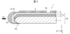
- FIG. 3 is a cross-sectional view taken along line III-III shown in FIG.
- the template substrate 7 in this embodiment includes a main substrate 1 containing silicon and having an edge E (end surface, side surface) and a main substrate 1 located above the main substrate 1. It includes a base portion 4, a mask 6 located above the main substrate 1 and having an opening KS, and a protective portion PS overlapping the edge E in a side view.
- the template substrate 7 may be provided with the buffer portion 2 and the seed portion 3 in order from the main substrate 1 side as the underlying portion 4 .
- the seed portion 3 may be positioned in the opening KS above the main substrate 1 .
- the protection part PS may contain a material different from gallium (Ga).
- the base portion 4, the buffer portion 2, the seed portion 3, and the mask 6 are typically layered. Therefore, the base portion 4 can also be called the base layer 4 . Also, the buffer portion 2 can be called the buffer layer 2 , the seed portion 3 can be called the seed layer 3 , and the mask 6 can be called the mask layer 6 . In the following description, these layers are referred to as an underlying layer 4, a buffer layer 2, a seed layer 3, and a mask layer 6, but they are not necessarily limited to layers.
- the main substrate 1 has an edge E (side surface, end face) with a non-uniform shape (angular shape) in a cross-sectional view.
- Such an edge E can be formed by a chamfering process in the manufacturing process of the main board 1 .
- the edge E of the main substrate 1 includes the curved surface portion Er and the flat surface portion Ef, but the edge E may be composed only of a curved surface or a flat surface.
- the main substrate 1 may have an edge E that is not chamfered.
- the template substrate 7 may have a plurality of layers laminated on the main surface 1a.
- the lamination direction in which a plurality of layers are laminated on the main surface 1a is defined as the "upward direction", and for a substrate-like object such as the template substrate 7, for example, a line of sight parallel to the normal line of the main surface 1a It is sometimes called "planar viewing".
- the object Viewing in the direction normal to the side surface (virtual plane) of an object is sometimes referred to as "side viewing".
- viewing the template substrate 7 from the side means viewing the template substrate 7 in the direction of arrow A1 shown in FIGS.
- the overlapping of two components in a side view means that at least a part of one component overlaps the other component when viewed in a direction perpendicular to the substrate normal of the template substrate 7 (including transparent viewing). They may overlap.
- the two components may be in contact or may be spaced apart without contact.
- two components overlap in plan view means that at least a part of one component overlaps the other component when viewed in the normal direction of the main substrate 1 (including perspective view). .
- Two components may be spaced apart (e.g., vertically) and overlapping.
- the template substrate 7 may have a buffer layer 2 and a seed layer 3 that overlap the entire main surface 1a of the main substrate 1 in plan view.
- the base substrate UK including the main substrate 1 and the base layer 4 may be referred to.
- a mask layer 6 formed on a base substrate UK has a plurality of mask portions 5 and a plurality of openings KS. Both the mask portion 5 and the opening KS have a longitudinal shape with the width direction in the first direction (X direction) and the longitudinal direction in the second direction (Y direction).
- the opening KS may have a tapered shape (a shape that narrows downward).
- the mask layer 6 may have a shape in which both ends in the longitudinal direction of the opening KS are open, that is, a shape in which the mask portions 5 do not exist at both ends in the longitudinal direction. It's okay.
- Mask layer 6 may be a mask pattern including mask portion 5 and opening KS.
- the opening KS is a region where the mask portion 5 does not exist, and the opening KS may not be surrounded by the mask portion 5 .
- both (main substrate and seed layer) may melt together. Therefore, for example, by providing the buffer layer 2 including at least one of an AlN layer and a SiC (silicon carbide) layer, the possibility of the main substrate 1 and the seed layer 3 melting each other can be reduced.
- the main substrate 1 that does not melt with the seed layer 3 is used, a configuration without the buffer layer 2 is also possible.
- the seed layer 3 with low reactivity with the main substrate 1 it is possible to adopt a configuration in which the buffer layer 2 is not provided. 2 and 3, the configuration in which the seed layer 3 overlaps the entire mask portion 5 is not limited. Since the seed layer 3 only needs to be exposed from the opening KS, the seed layer 3 may be locally formed so as not to partially or wholly overlap the mask portion 5 .
- Mask layer 6 may be formed, for example, as follows. That is, after a SiO 2 film is formed on the entire surface of the underlying substrate UK using a sputtering method, wet etching is performed while partially protecting it with a resist. A mask portion 5 and an opening KS are formed by removing a portion of the SiO 2 film. Generally, the side surfaces of the base substrate UK are not covered by a SiO2 film. This is due to (i) insufficient coverage of the SiO 2 film on the side surfaces of the underlying substrate UK in the sputtering method, and (ii) the resist is not sufficiently applied to the side surfaces of the underlying substrate UK unless the resist is intentionally applied, so that the SiO 2 film formed by etching can be removed. 2 film is removed.
- the template substrate 7 can be used for forming a semiconductor portion, for example, for depositing a GaN-based semiconductor portion by the ELO method.
- a GaN-based semiconductor is a semiconductor containing gallium atoms (Ga) and nitrogen atoms (N), and examples thereof include GaN, AlGaN, AlGaInN, and InGaN.
- a seed layer 3 containing a GaN-based semiconductor is used, an inorganic compound film such as a SiO 2 film is used as a mask layer 6 , and a GaN-based semiconductor portion can be laterally grown on the mask portion 5 .
- the thickness direction (Z direction) of the GaN-based semiconductor portion is the ⁇ 0001> direction (c-axis direction) of the GaN-based crystal, and the width direction (X-direction) of the opening KS is the ⁇ 11-20> direction (a-axis) of the GaN-based crystal. direction), and the longitudinal direction (Y direction) of the opening KS can be the ⁇ 1-100> direction (m-axis direction) of the GaN-based crystal.
- the GaN-based semiconductor portion is typically layered. Therefore, the GaN-based semiconductor portion can also be called a GaN-based semiconductor layer.
- the GaN-based semiconductor layer is referred to as a GaN-based semiconductor layer, but the GaN-based semiconductor layer is not necessarily limited to a layered structure.
- a layer formed by the ELO method is sometimes called an ELO semiconductor layer.
- meltback etching SMB may occur as described above. Although the reason for this is not clear, it is considered as follows.
- the buffer layer 2 is formed under conditions that do not prevent the film forming raw material from wrapping around the side surface of the main substrate 1 (covering the side surface). As such, it is difficult to be formed so as to cover the side surface of the main substrate 1 . Therefore, it is considered that the layer thickness of the buffer layer 2 is uneven at the side surface portion of the template substrate 7 due to the uneven side surface shape of the main substrate 1, thinning of the buffer layer 2, and the like. As a result, it is thought that there may be a portion where the main substrate 1 and the seed layer 3 are not sufficiently separated by the buffer layer 2 .
- the buffer layer 2 is too thin on the side surface of the template substrate 7, the buffer layer 2 is cracked, and the main substrate 1 cannot be completely (effectively) protected by the buffer layer 2. It is conceivable that there may be microscopic regions where there is no Hereinafter, in this specification, the location (the minute area) that can be the starting point of the meltback etching SMB is referred to as "abnormal location DP".
- the layer thickness of the buffer layer 2 on the side surface portion of the template substrate 7 is increased, the layer thickness of the buffer layer 2 on the main surface 1a of the main substrate 1 is also increased. can impair function. Specifically, cracks may occur in the buffer layer 2 due to the internal stress of the buffer layer 2 and the stress caused by the difference in thermal expansion coefficient and lattice constant between the buffer layer 2 and the main substrate 1 . As a result, meltback etching between the main substrate 1 and the seed layer 3 may occur through the crack. Therefore, the layer thickness of the buffer layer 2 cannot be increased freely.
- the film formation conditions for forming the ELO semiconductor layer affect the state of occurrence of meltback etching SMB. For example, if the film formation temperature exceeds 1050° C. in order to secure the film formation speed in the lateral direction, meltback etching SMB is likely to occur. In addition, if the film formation time is relatively long, the area of the region where the meltback etching SMB occurs expands.
- the template substrate 7 in one aspect of the present disclosure can be configured to include a protective portion PS formed along the outer periphery of the base substrate UK.
- the protective portion PS covers the side surface (end surface) of the base substrate UK and overlaps the edge E of the main substrate 1 in a side view.
- the protective portion PS includes, for example, a nitride film containing silicon, an oxide film containing silicon, or an oxynitride film containing silicon.
- the protection part PS may typically include a silicon nitride (SiN) film or a SiO2 film.
- the protection part PS may contain a material different from gallium (Ga), more specifically, a material different from elemental Ga and a Ga compound (hereinafter referred to as a non-Ga-based material for convenience of explanation).
- Ga gallium
- Non-Ga-based materials included in the protective portion PS include, for example, silicon nitride, silicon oxide, silicon oxynitride, aluminum silicon oxide, and the like.
- the protection part PS may contain a plurality of types of the above non-Ga-based materials.
- the protective portion PS may contain a larger amount of the non-Ga-based material than Ga. may be more.
- the content of the non-Ga-based material in the protective portion PS means the total content of all types of non-Ga-based materials included in the protective portion PS when a plurality of types of non-Ga-based materials are included.
- the protection part PS may be an inorganic insulating film or an inorganic insulating layer that does not contain Ga or does not substantially contain Ga. “Substantially free of Ga” means that Ga may be mixed in the protection portion PS as an unavoidable impurity, and even if Ga mixed in the protection portion PS by diffusion of atoms from the seed layer 3 is contained, means good.
- the protective portion PS only needs to have the function of reducing the occurrence of meltback etching SMB in the side portion of the template substrate 7, and may contain Ga within an allowable concentration range.
- the protective portion PS may contain Ga at a molar ratio of 1% or less in the component composition.
- the protection part PS may be formed using, for example, a CVD (Chemical Vapor Deposition) method, a plasma CVD method, or the like, or may be formed by other methods.
- CVD Chemical Vapor Deposition
- plasma CVD plasma CVD method
- the distance from the lowest position to the highest position of the protective portion PS in the thickness direction (Z direction) of the template substrate 7 is defined as a height H
- the thickness of the main substrate 1 is t1
- the base layer 4 is t2.
- the protection part PS may have a height H that is greater than the plate thickness t1, and may have a height H that is greater than the sum of the plate thickness t1 and the layer thickness t2.
- the height H may be, for example, 200 ⁇ m or more and 1200 ⁇ m or less, or 300 ⁇ m or more and 1100 ⁇ m or less.
- the ridgeline (intersection point in cross section) where the edge E of the main substrate 1 and the main surface 1a intersect is RH
- the ridgeline (intersection point in cross section) where the edge E of the main substrate 1 and the lower surface 1b intersect is RL.
- a side portion of the base substrate UK located on the outer peripheral side of the ridge line RH (located on the side farther from the central portion) is referred to as a side portion SP of the base substrate UK.
- the side surface portion SP of the base substrate UK is a portion including the main substrate 1, the buffer layer 2 and the seed layer 3 located outside the main surface 1a in the XY plane (planar view).
- the protective portion PS may be in contact with the seed layer 3 or may cover the entire surface of the seed layer 3 at the side surface portion SP of the base substrate UK.
- the protective portion PS may cover the side surface portion SP of the base substrate UK from the position of the lower surface 1b (in other words, the position of the ridgeline RL) in the Z direction to the position of the main surface 1a (in other words, the position of the ridgeline RH), In this case, the protective portion PS overlaps the entire edge E in a side view.
- the protective portion PS may cover the side surface portion SP of the base substrate UK from the position of the lower surface 1b in the Z direction to the position of the main surface 1a of the seed layer 3 (in other words, the position of the ridge line RH).
- the side portion SP may be covered so that the seed layer 3 is not exposed at the side portion SP. Moreover, part of the side surface portion SP and the mask portion 5 may be in contact with each other.
- the term “contact” between two different members means not only direct contact with each other, but also some other thin layer (for example, a thickness of 2 ⁇ m or less and a single layer It also means that they may be in indirect contact via an intervening layer.
- the template substrate 7 has a protective portion PS.
- the use of the template substrate 7 prevents Ga, which is supplied from the Ga raw material, from reaching the main substrate 1 when the ELO semiconductor layer is formed by the ELO method. Therefore, it is possible to reduce the possibility that the Ga supplied from the Ga raw material reacts with the main substrate 1 via the abnormal portion DP.
- the seed layer 3 and the main substrate 1 may react due to the absence of the buffer layer 2 or the thickness of the buffer layer 2 being thin.
- the layer thickness of the buffer layer 2 is thin, Ga can permeate the buffer layer 2 .
- the reaction can be limited to a local reaction between the seed layer 3 and the main substrate 1 at the abnormal point DP because there is no new supply of Ga to the reaction point. can.
- meltback etching SMB it is possible to reduce the possibility of the reaction itself occurring due to the fact that Ga is not supplied to the abnormal portion DP from the outside. As a result, the possibility of occurrence of meltback etching SMB can be reduced, and even if meltback etching SMB occurs, the area of the region where meltback etching SMB occurs can be reduced.
- the portion where the distance between the surface of the protective portion PS and the surface of the seed layer 3 is the shortest in other words, the portion of the protective portion PS closest to the surface of the seed layer 3 (the thinnest portion) has a thickness of 100 nm. or more. This can effectively reduce the possibility of Ga being supplied to the abnormal point DP.
- the lowest position of the protective portion PS in the Z direction may be lower than the position of the lower surface 1b (in other words, the position of the ridge line RL). may be in contact with Moreover, the protective portion PS may cover at least a portion of the lower surface 1b including the ridgeline RL. In other words, the protection part PS may overlap a part of the lower surface 1b when viewed with a line of sight parallel to the normal to the lower surface 1b.
- the portion of the protective portion PS that covers the lower side (lower surface 1b side) of the template substrate 7 may be referred to as a lower protective portion PS1.
- the lower protector PS1 may be part of the protector PS.
- the buffer layer 2 and the seed layer 3 may slightly wrap around the bottom surface 1b.
- the buffer layer 2 and the seed layer 3 may cover a part of the lower surface 1b, and the ends of the buffer layer 2 and the seed layer 3 on the outer peripheral side extend from the ridgeline RL to the Y distance. It may be located at a position of several ⁇ m in the direction.
- the end portion of the lower protective portion PS1 on the center side of the template substrate 7 is referred to as PSE.
- PSE the end portion of the lower protective portion PS1 on the center side of the template substrate 7
- W1 be the distance between the position closest to the center of the template substrate 7 and the position of the end PSE.
- the distance W1 in the lower protective portion PS1 may be, for example, 1 ⁇ m or more. can be reduced to As a result, the possibility of occurrence of meltback etching SMB can be further reduced.
- the distance W1 of the lower protection part PS1 may be, for example, 1 ⁇ m or more and 5000 ⁇ m or less.
- Such a lower protective part PS1 can be formed by forming the protective part PS using, for example, the plasma CVD method.
- protective portions PS can be provided outside the side surfaces of the main substrate 1 so that the main substrate 1 is not exposed on the side surfaces of the template substrate 7 .
- the material of the protection part PS may be a semiconductor that does not contain gallium, such as AlN or SiC, or an amorphous material such as SiNx.
- a nitride semiconductor (for example, a GaN-based semiconductor) may be positioned between the side surface of the main substrate 1 and the protective portion PS.
- the side surface of the main substrate 1 and the protection part PS may be in contact with each other.
- the protective part PS may have a shape that wraps around the main substrate 1 from above to the side.
- the protective portion PS may be formed in the same layer as the mask portion 5 or in a layer above the mask portion 5 .
- a thermally oxidized film of the main substrate 1 may be used as the protective portion PS.
- the distance between the longitudinal opening KS and the side surface of the template substrate 7 may be larger than the width of the opening KS.
- the distance between the seed layer 3 and the side surface of the template substrate 7 may be larger than the width of the opening K.
- FIG. 4 is a cross-sectional view for explaining the semiconductor substrate 10 of this embodiment.
- FIG. 4 shows a cross section corresponding to FIG. 3 and an example of lateral growth.
- the initial growth layer SL is formed starting from the seed layer 3 exposed in the opening KS. Then, the initial growth layer SL is further grown and laterally grown to form the ELO semiconductor section 8 .
- the ELO semiconductor portion 8 contains, for example, a GaN-based semiconductor.
- the semiconductor substrate 10 may have the functional portion 9 formed above the ELO semiconductor portion 8 .
- the functional part 9 may be a single layer body or a multilayer body.
- the functional part 9 has a function as a component of a semiconductor device, a light emitting function, a protection function from external forces, a protection function from static electricity, a protection function to prevent foreign substances such as water and oxygen from entering, a protection function from etchants and the like, and an optical function. and at least one of a sensing function.
- the ELO semiconductor portion 8 and the functional portion 9 are typically layered. Therefore, the ELO semiconductor portion 8 can also be called the ELO semiconductor layer 8 , and the functional portion 9 can be called the functional layer 9 . In the following description, the ELO semiconductor layer 8 and the functional layer 9 are referred to, but the ELO semiconductor layer 8 and the functional layer 9 are not necessarily limited to layers.
- the ELO semiconductor layer 8 includes an effective portion EK, which overlaps the mask portion 5 in plan view and has relatively few threading dislocations, and a non-effective portion NS, which overlaps the opening portion KS in plan view and has relatively many threading dislocations.
- the functional layer 9 includes an active layer (for example, a layer in which electrons and holes combine) in a layer above the ELO semiconductor layer 8, on the effective portion EK (in other words, a position overlapping the effective portion EK in plan view)
- the functional layer 9 can be formed so as to include an active layer with few defects and high crystallinity.
- a current injection region can be formed in this effective portion EK to form a device in which the active layer functions. Thereby, for example, a device with high luminous efficiency can be manufactured.
- the effective portion EK can be configured such that the non-threading dislocation density in the cross section parallel to the ⁇ 0001> direction is higher than the threading dislocation density in the upper surface.
- Threading dislocations are dislocations (defects) that extend from the lower surface or inside of the ELO semiconductor layer 8 to its surface or surface layer along the thickness direction (Z direction) of the ELO semiconductor layer 8 . Threading dislocations can be observed by performing CL (Cathode Luminescence) measurement on the surface (parallel to the c-plane) of the ELO semiconductor layer 8 .
- Non-threading dislocations are dislocations that are CL-measured in a cross section along a plane parallel to the thickness direction, and are mainly basal plane (c-plane) dislocations.
- FIG. 5A is a partially enlarged plan view showing the configuration of the semiconductor substrate 10.
- FIG. 5B is a cross-sectional view taken along line BV shown in FIG. 5A. 5A and 5B show the semiconductor substrate 10 before the functional layer 9 is formed.
- the ELO semiconductor layer 8 grown from the opening KS by the ELO method is the semiconductor substrate 10 side. It can be formed so as to wrap around to one side. This is because the ELO semiconductor layer 8 also grows in the Y direction (the m-axis direction of the GaN-based crystal) at a slower growth rate than in the X direction. In particular, the ELO semiconductor layer 8 tends to wrap around to the sides of the semiconductor substrate 10 when the film is formed under conditions that increase the width of the effective portion EK.
- the semiconductor substrate 10 includes the protective portion PS, the possibility of meltback etching SMB occurring under the film formation conditions of the ELO semiconductor layer 8 can be effectively reduced. Therefore, the effective area of the effective portion EK in the semiconductor substrate 10 can be increased. As a result, the yield of devices manufactured using the semiconductor substrate 10 can be improved.
- the semiconductor substrate 10 may include a protective portion PS including the lower protective portion PS1. Even when the raw material gas is supplied, the possibility of Ga coming into contact with the main substrate 1 can be reduced. Therefore, the possibility of occurrence of meltback etching SMB can be effectively reduced.
- the semiconductor substrate 10 may have an ELO semiconductor layer 8 formed by combining semiconductor films laterally grown in opposite directions from adjacent openings KS, and the ELO semiconductor layer 8 is a mask. A configuration (meeting type) having no edge on the portion 5 may be used.
- the semiconductor substrate 10 may have a functional layer 9 on the association type ELO semiconductor layer 8 .
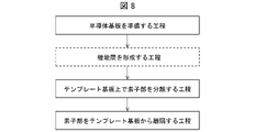
- FIG. 6 is a flow chart showing an example of a method for manufacturing the semiconductor substrate 10 according to this embodiment.
- the flow chart shown in FIG. 6 can also include a method for manufacturing the template substrate 7 .
- a base substrate UK is prepared.
- This base substrate UK may be produced by forming a base layer 4 on the main substrate 1 .
- the template substrate 7 is manufactured by performing the step of forming the protective portion PS.
- the mask layer 6 may be formed after forming the protective portion PS.
- the step of forming the mask layer 6 may include the step of forming the protection portion PS.
- a step of forming an ELO semiconductor layer 8 on the template substrate 7 using the ELO method is performed. After the step of forming the ELO semiconductor layer 8, the step of forming the functional layer 9 can be performed as required.
- FIG. 7 is a block diagram showing an example of the manufacturing apparatus 70 in this embodiment.
- the manufacturing apparatus 70 includes a mask layer forming portion 71 for forming the mask layer 6 on the underlying substrate UK, a protective portion forming portion 72 for forming the protective portion PS, and an ELO semiconductor on the template substrate 7 . and a semiconductor layer forming portion 73 for forming the layer 8 .
- the manufacturing apparatus 70 also includes a control section 74 that controls the mask layer forming section 71 , the protective section forming section 72 , and the semiconductor layer forming section 73 .
- the mask layer forming section 71 may include one or more devices that perform various processes for forming the mask layer 6 on the base substrate UK, and known devices can be applied as the devices.
- the protection part forming part 72 may have a configuration in which a plurality of known devices are combined so as to form the protection part PS.
- the protective part forming part 72 may include a plasma CVD device.
- the semiconductor layer forming section 73 forms the ELO semiconductor layer 8 (see FIG. 4 etc.) containing a GaN-based semiconductor by the ELO method so as to be in contact with the seed layer 3 and the mask section 5 .
- the semiconductor layer forming section 73 may include an MOCVD (metal-organic CVD) device.
- the manufacturing apparatus 70 may be configured to form the functional layer 9 or may be configured to form the underlying layer 4 on the main substrate 1 .
- the control unit 74 may include a processor and memory.
- the control unit 74 executes a program stored in, for example, an internal memory, a communicable communication device, or an accessible network to control the mask layer forming unit 71, the protection unit forming unit 72, and the semiconductor layer forming unit. 73 may be controlled.
- the above program and a recording medium storing the above program are also included in this embodiment.
- FIG. 8 is a flow chart showing an example of a method for manufacturing a semiconductor device according to this embodiment.
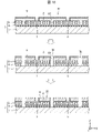
- FIG. 9 is a plan view showing an example of separation of the element section.
- FIG. 10 is a cross-sectional view showing an example of separation and separation of element portions.
- the step of forming the functional layer 9 on the ELO semiconductor layer 8 is performed as necessary. Thereafter, as shown in FIGS. 9 and 10, a plurality of trenches TR (separation grooves) are formed in the semiconductor substrate 10 to isolate the element portion DS (including the effective portion EK of the ELO semiconductor layer 8 and the functional layer 9). carry out the process.
- the element portion DS is connected to the substrate (underlying substrate UK) at the opening KS, and the back surface of the element portion DS and the mask portion 5 are weakly coupled to each other by van der Waals force in the effective portion EK.
- a trench TR (separation groove) is formed over the opening KS, the trench TR is formed so that the trench bottom is lower than the surface height of the mask portion 5, and the opening width of the trench TR is equal to the opening KS , the element part DS can be easily separated from the substrate.
- Trench TR penetrates functional layer 9 and ELO semiconductor layer 8 .
- Mask portion 5 and main substrate 1 may be exposed in trench TR.
- the element portion DS is separated from the template substrate 7, and a step of forming a semiconductor device is performed.
- the step of preparing the semiconductor substrate 10 of FIG. 8 may include each step of the method of manufacturing the template substrate 7 and the semiconductor substrate 10 shown in FIG.
- the template substrate 7 may include an underlying substrate UK and a mask pattern on the underlying substrate UK.
- the template substrate 7 may have a growth suppression region (for example, a region that suppresses crystal growth in the Z direction) corresponding to the mask portion 5 and a seed region corresponding to the opening KS.
- a growth suppression region and a seed region on the underlying substrate UK, and form the ELO semiconductor layer 8 on the growth suppression region and the seed region using the ELO method.
- the semiconductor device 20 As shown in FIG. 10, by separating the element part DS from the template substrate 7, the semiconductor device 20 (including the ELO semiconductor layer 8) can be formed. For example, after separating the element part DS from the template substrate 7, an n-electrode or the like may be formed on the rear surface of the separated element part DS.
- the semiconductor device 20 include light emitting diodes (LEDs), semiconductor lasers, Schottky diodes, photodiodes, transistors (including power transistors and high electron mobility transistors), and the like.
- FIG. 11 is a schematic diagram showing the configuration of an electronic device according to this embodiment.
- the electronic device 30 of FIG. 11 includes a semiconductor substrate 10 (a configuration that functions as a semiconductor device while including the template substrate 7, for example, when the template substrate 7 is translucent), and a drive substrate on which the semiconductor substrate 10 is mounted. 23 and a control circuit 25 that controls the drive board 23 .
- FIG. 12 is a schematic diagram showing another configuration of the electronic device according to this embodiment.
- An electronic device 30 of FIG. 12 includes a semiconductor device 20 including at least an effective portion EK, a drive board 23 on which the semiconductor device 20 is mounted, and a control circuit 25 that controls the drive board 23 .
- Examples of the electronic device 30 include a display device, a laser emitting device (including a Fabry-Perot type and a surface emitting type), a lighting device, a communication device, an information processing device, a sensing device, a power control device, and the like.
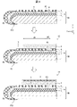
- FIGS. 13A and 13B are cross-sectional views showing the configuration of a template substrate 7 according to another embodiment of the present disclosure.
- 13A shows a cross section corresponding to FIG. 2
- FIG. 13B shows a cross section corresponding to FIG.
- the template substrate 7 may not have the buffer layer 2 on the side surface portion SP of the base substrate UK.
- the template substrate 7 has the protection part PS, so that when the ELO semiconductor layer 8 is formed by the ELO method, the Ga derived from the Ga raw material is mainly used.
- the possibility of reaching the substrate 1 can be reduced.
- the possibility of occurrence of meltback etching SMB can be reduced, and even if meltback etching SMB occurs, the area of the region where meltback etching SMB occurs can be reduced.
- the template substrate 7 in another embodiment of the present disclosure may be configured without the buffer layer 2 as described above. you can Regarding the template substrate 7 without the buffer layer 2 in one embodiment, the following can be said.
- the above description of the abnormal portion DP can be understood by replacing the buffer layer 2 with the seed layer 3 as appropriate.
- the material used for the buffer layer 2 may be used as the material for the seed layer 3, and the seed layer 3 may have an abnormal point DP.
- the template substrate 7 has the protection part PS, so that when the ELO semiconductor layer 8 is formed by the ELO method, the Ga derived from the Ga raw material is mainly used. The possibility of reaching the substrate 1 can be reduced. As a result, the possibility of occurrence of meltback etching SMB can be reduced, and even if meltback etching SMB occurs, the area of the region where meltback etching SMB occurs can be reduced.
- the template substrate 7 having the buffer layer 2 on the side surface portion SP of the base substrate UK will be described as an example.
- the template substrate 7 may be configured without the buffer layer 2 on the side surface portion SP of the base substrate UK.
- the template substrate 7 in each example may not have the buffer layer 2 on the side surface portion SP of the underlying substrate UK unless otherwise specified. are also within the scope of this disclosure.
- FIG. 14 is a plan view showing the configuration of the template substrate 7 in Example 1.
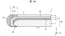
- FIG. 15A is a cross-sectional view taken along line A-XV shown in FIG. 14.
- FIG. 15B is a cross-sectional view taken along line B-XV shown in FIG. 14.
- FIG. 15A is a cross-sectional view taken along line A-XV shown in FIG. 14.
- template substrate 7 in Example 1 includes main substrate 1, base layer 4, and mask layer 6.
- Mask layer 6 defines protective portion PS. It has a mask portion 5 containing.
- the protective portion PS and the mask portion 5 may be integrated with each other.
- the main substrate 1 is a substrate containing silicon, and a substrate (heterogeneous substrate) made of a material different from the GaN-based semiconductor can be used.
- the main substrate 1 may typically be a silicon substrate, or may be a silicon-based substrate containing silicon as a main component.
- the main substrate 1 may be, for example, a silicon-based substrate containing 90% or more of silicon in molar ratio, or may be a silicon-based substrate containing 95% or more of silicon.
- the main substrate 1 may be a single crystal substrate or an amorphous substrate.
- the plane orientation of the main substrate 1 may be, for example, the (111) plane or the (100) plane of the silicon substrate.
- the main substrate 1 may be made of a material containing silicon and have a plane orientation that allows the ELO semiconductor layer 8 to be grown by the ELO method.
- the main substrate 1 may be a silicon carbide (SiC; silicon carbide) substrate, but the SiC substrate has relatively low reactivity with Ga. Therefore, the SiC substrate inherently has the property of being resistant to meltback etching SMB. Therefore, the main substrate 1 may be a substrate other than the SiC substrate containing silicon.
- the edge E of the main substrate 1 has a curved surface portion Er and a flat surface portion Ef connected to the curved surface portion Er and having a normal line parallel to the X direction, but is not limited to this.
- the main substrate 1 may be disc-shaped.
- the plane portion Ef may have a function as a plane orientation indicator (orientation flat).
- the orientation indicator can also be configured with a notch (notch).
- the template substrate 7 may be provided with a buffer layer 2 and a seed layer 3 in this order from the main substrate 1 side as the underlying layer 4 .
- it has the buffer layer 2 and the seed layer 3 which were formed so that it may overlap with the whole surface of the main surface 1a of the main board
- the buffer layer 2 has a function of, for example, reducing the contact between the main substrate 1 and the seed layer 3 and their mutual melting.
- the buffer layer 2 is provided between the silicon substrate and the GaN-based semiconductor so that the silicon substrate and the GaN-based semiconductor are mutually connected. Melting can be reduced.
- the buffer layer 2 may have at least one of the effect of increasing the crystallinity of the seed layer 3 and the effect of relieving the internal stress of the seed layer 3 .
- the buffer layer 2 may typically be an AlN layer or may be a SiC layer.
- SiC used for the buffer layer 2 may be of a hexagonal system (6H--SiC, 4H--SiC) or a cubic system (3C--SiC).
- Buffer layer 2 may be a multilayer film including at least one of an AlN film and a SiC film.
- the buffer layer 2 may contain a strain relaxation layer. Examples of the strain relaxation layer include an AlGaN superlattice structure and a graded structure in which the Al composition of AlGaN is changed stepwise. The stress in the longitudinal direction of the ELO semiconductor layer 8 can be relaxed by the strain relief layer.
- An AlN layer which is an example of the buffer layer 2 can be formed to a thickness of about 10 nm to about 5 ⁇ m using, for example, an MOCVD apparatus.
- the buffer layer 2 may contain a Ga composition of 1% or less. Ga may be inevitably introduced into the buffer layer 2 by atomic diffusion of Ga.
- the seed layer 3 is a layer that serves as a growth starting point for the ELO semiconductor layer 8 when the ELO semiconductor layer 8 is formed.
- a GaN-based semiconductor, aluminum nitride (AlN), silicon carbide (SiC), graphene, or the like can be used for the seed layer 3 .
- the silicon carbide used for the seed layer 3 may be hexagonal 6H--SiC or 4H--SiC.
- the seed layer 3 may be, for example, an AlGaN layer, or may be a graded layer whose Al composition approaches GaN.
- the graded layer is, for example, a laminate in which a first Al0.7Ga0.3N layer and a second Al0.3Ga0.7N layer are provided in order from the AlN layer side.
- the graded layer can be easily formed by MOCVD, and may be composed of three or more layers.
- the seed layer 3 can be configured to include a GaN layer.
- the seed layer 3 may be a single layer of GaN, or the uppermost layer of the graded layer that is the seed layer 3 may be a GaN layer.
- buffer layer 2 eg, aluminum nitride
- seed layer 3 eg, GaN-based semiconductor
- PSD pulse sputter deposition
- PLD pulse laser deposition
- the underlying layer 4 can be formed by stacking various layers on the main substrate 1 using an MOCVD device, a sputtering device, or the like.
- the buffer layer 2 is generally not sufficiently formed on the edge E of the main substrate 1 . Therefore, the aforementioned abnormal portion DP may exist in the side surface portion SP of the base substrate UK.
- the opening KS has a longitudinal shape, and a plurality of openings KS may be arranged periodically with a first period in the a-axis direction (X direction) of the ELO semiconductor layer 8 .
- the width of the opening KS may be about 0.1 ⁇ m to 20 ⁇ m. As the width of the opening KS becomes smaller, the number of threading dislocations propagating from the opening KS to the ELO semiconductor layer 8 decreases. Also, the ELO semiconductor layer 8 can be easily peeled off in a post-process. Furthermore, the area of the effective portion EK with few surface defects can be increased.
- the mask layer 6 having the mask portion 5 including the protective portion PS may be formed, for example, as follows. First, a silicon oxide film having a thickness of about 100 nm to 4 ⁇ m (preferably about 150 nm to 2 ⁇ m) is formed on the underlying layer 4 by sputtering. At this time, in Example 1, the silicon oxide film is also formed on the side surface portion SP of the underlying substrate UK. Then, in Example 1, a resist is applied to the entire surface of the silicon oxide film including the silicon oxide film formed on the side surface portion SP of the underlying substrate UK. After that, the resist is patterned by photolithography to form a resist having a plurality of striped openings.
- Example 1 the resist covering the silicon oxide film formed on the side surface portion SP of the base substrate UK is not removed. After that, by removing part of the silicon oxide film with a wet etchant such as hydrofluoric acid (HF) or buffered hydrofluoric acid (BHF), a mask portion 5 including a plurality of openings KS and protective portions PS is formed. . A mask layer 6 is then formed by removing the resist with an organic wash.
- a wet etchant such as hydrofluoric acid (HF) or buffered hydrofluoric acid (BHF)
- the mask portion 5 may include a protective portion PS having a lower protective portion PS1.
- a protective portion PS having a lower protective portion PS1 For example, by using the plasma CVD method, it is easy to form the mask portion 5 so as to wrap around the lower side of the underlying substrate UK.
- a layered body was used in which a silicon oxide film (SiO 2 ) and a silicon nitride film (SiN) were formed in this order.
- the thickness of the silicon oxide film is, for example, 0.3 ⁇ m, and the thickness of the silicon nitride film is, for example, 70 nm.
- a mask layer 6 was formed to have a mask portion 5 including a protective portion PS.
- a plasma CVD method was used to form each of the silicon oxide film and the silicon nitride film.
- the semiconductor substrate 10 includes a template substrate 7 and an ELO semiconductor layer 8 positioned above the mask layer 6 .
- a semiconductor substrate means a substrate that includes a semiconductor layer.
- the ELO semiconductor layer 8 may be doped (eg, n-type containing donors or p-type containing acceptors) or non-doped. Examples of the donor include silicon and germanium, and examples of the acceptor include magnesium. ELO semiconductor layer 8, if doped, may contain both donors and acceptors.
- the ELO semiconductor layer 8 contains, for example, a nitride semiconductor.
- a GaN layer was used as the ELO semiconductor layer 8, and an ELO film was formed on the template substrate 7 of Example 1 using an MOCVD apparatus.
- substrate temperature 1120° C.
- growth pressure 50 kPa
- TMG trimethylgallium
- NH 3 15 slm
- An ELO semiconductor layer 8 is selectively grown on the seed layer 3 (the uppermost GaN layer of the seed layer 3) exposed in the opening KS, and subsequently laterally grown on the mask portion 5. As shown in FIG. Then, the lateral growth was stopped before the ELO semiconductor layers 8 growing laterally on both sides of the mask portion 5 joined together.
- the width of the mask portion 5 is 50 ⁇ m
- the width of the opening KS is 5 ⁇ m
- the lateral width of the ELO semiconductor layer 8 is 53 ⁇ m
- the width of the effective portion EK size in the X direction
- the layer thickness of the ELO semiconductor layer 8 is 5 ⁇ m. rice field.
- the lateral film formation rate is increased.
- Methods for increasing the lateral film formation rate are, for example, as follows. First, a vertical growth layer (initial growth layer SL) growing in the Z direction (c-axis direction) is formed on the seed layer 3 exposed from the opening KS. Form a growth layer. At this time, by setting the thickness of the vertical growth layer to 10 ⁇ m or less, preferably 5 ⁇ m or less, and more preferably 3 ⁇ m or less, the thickness of the horizontal growth layer can be kept low and the horizontal film formation rate can be increased.
- the area of the region where the meltback etching SMB occurred was relatively reduced.
- the possibility of occurrence of meltback etching SMB in the semiconductor substrate 10 could be reduced as compared with the case of using a conventional template substrate having no protective portion PS.
- FIG. 16 is a plan view showing the configuration of the template substrate 7 in Example 2.
- FIG. 17A is a cross-sectional view taken along line A-XVII shown in FIG. 16.
- FIG. 17B is a cross-sectional view taken along line B-XVII shown in FIG. 16.
- FIG. 17A is a cross-sectional view taken along line A-XVII shown in FIG. 16.
- Example 1 the mask layer 6 having the mask portion 5 including the protection portion PS was formed on the base substrate UK, but in Example 2, the protection portion PS is provided separately from the mask portion 5. It's okay.
- the template substrate 7 in Example 2 has a main substrate 1, an underlying layer 4, a mask layer 6, and a protective portion PS.
- the protection part PS may have a material different from that of the mask part 5 .
- the protection part PS may include an inorganic insulating film or an inorganic insulating layer that does not contain Ga or substantially does not contain Ga.
- the protection part PS may be, for example, a resin member, a metal member, or a ceramic member that does not contain Ga or does not substantially contain Ga.
- the protective part PS may be made of an appropriate material that can reduce the possibility of occurrence of meltback etching SMB, and the specific material is not particularly limited.
- the protection part PS may have a shape that fits into the side surface of the base substrate UK. may be covered.
- the protective portion PS may cover at least a portion of the mask portion 5 and may enter at least a portion of the opening KS on the upper surface of the underlying substrate UK. That is, the protective portion PS may overlap the edge E in a side view and may overlap at least a portion of the main surface 1a in a plan view.
- the protection part PS may cover at least part of the lower surface 1b, ie, may have a lower protection part PS1.
- the thickness t3 of the protective portion PS may be larger than the thickness of the mask portion 5 in the layer above the main surface 1a.
- the thickness t3 may be, for example, 0.05 ⁇ m or more and 3 ⁇ m or less.
- the protection part PS can be additionally formed in the peripheral portion of the base substrate UK.
- the mask layer 6 may be formed after forming the protective portion PS in the peripheral portion of the underlying substrate UK.
- the template substrate 7 may be formed by mounting a protective portion PS formed in advance so as to cover the peripheral portion of the base substrate UK.
- the material, shape, thickness, etc. of the protective portion PS can be adjusted relatively easily, and the protective portion PS can have the lower protective portion PS1.
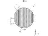
- FIG. 18 is a plan view showing the configuration of the template substrate 7 in Example 3.
- FIG. 19 is a cross-sectional view taken along line XIX-XIX shown in FIG. 18.
- FIG. 19 is a cross-sectional view taken along line XIX-XIX shown in FIG. 18.
- the mask layer 6 has an edge-to-edge shape, but it is not limited to this.
- the mask layer 6 may have a shape in which the mask portions 5 are present at both longitudinal ends of the opening KS.
- the template substrate 7 in Example 3 has a main substrate 1, an underlying layer 4, and a mask layer 6.
- the mask layer 6 is a mask portion including a protective portion PS. has 5.
- the opening KS has a longitudinal shape, and in plan view, a distance D1 is provided between the tip KE of the opening KS and the edge E of the main substrate 1 (in other words, the position of the ridge line RH described above). may have.
- Example 3 in the same method as in Example 1 described above, when patterning the resist using photolithography, the shape of the opening is slightly changed and the resist is etched to form the mask layer 6 . Just do it.
- Example 3 when the ELO semiconductor layer 8 is formed on the template substrate 7, the following can be said about the cross section shown in FIG. 19, for example. That is, since the tip KE of the opening KS is located at the position having the distance D1, the growth starting point of the ELO semiconductor layer 8 can be set at a position relatively distant from the edge E of the main substrate 1. FIG. Therefore, it is possible to reduce the possibility that the ELO semiconductor layer 8 is formed so as to wrap around the sides of the semiconductor substrate 10 .
- the interval D1 may be 1 ⁇ m or more and may be 1 ⁇ m or more and 6000 ⁇ m or less. Setting the distance D1 to 1 ⁇ m or more can further reduce the possibility that the ELO semiconductor layer 8 is formed so as to wrap around the sides of the semiconductor substrate 10 .
- the additional supply of Ga derived from the Ga raw material to the side surface portion SP of the base substrate UK can be made difficult.
- the reaction can be limited to a local reaction between the seed layer 3 and the main substrate 1 at the abnormal point DP. Therefore, the possibility of occurrence of meltback etching SMB can be reduced.
- FIG. 20 is a cross-sectional view showing the configuration of the template substrate 7 in Example 4. As shown in FIG.
- a protective portion PS may be further formed.
- the first protective portion overlapping the edge E of the main substrate 1 in side view It may comprise an FPS and a second protection part SPS.
- the mask layer 6 may have the mask portion 5 including the first protective portion FPS. That is, the first protective portion FPS and the mask portion 5 may be integrated.
- the first protective part FPS may be formed to cover the side part SP of the base substrate UK.
- a second protector SPS that covers the first protector FPS may be provided.
- the second protective part SPS may have a different material than the mask part 5 .
- the first protective portion FPS may be formed, for example, in the same manner as in Example 1 described above.
- the second protective portion SPS may be formed, for example, in the same manner as the protective portion PS of the second embodiment described above.
- the first protective part FPS may cover at least part of the lower surface 1b of the main substrate 1, ie, may have a lower protective part PS1.
- the second protector SPS may have the lower protector PS1.
- at least one of the first protector FPS and the second protector SPS may have the lower protector PS1.
- Example 4 when the ELO semiconductor layer 8 is formed on the template substrate 7, the following can be said about the cross-sectional portion shown in FIG. 20, for example. That is, in Example 4, the side surface portion SP of the base substrate UK is protected by both the first protection portion FPS and the second protection portion SPS. As a result, even if a reaction occurs at the above-described abnormal site DP, new supply of Ga to the reaction site can be effectively reduced by the first protector FPS and the second protector SPS. Therefore, the reaction between the seed layer 3 and the main substrate 1 at the abnormal point DP can be limited to a local reaction. As a result, the possibility of occurrence of meltback etching SMB can be highly reduced. Moreover, even if meltback etching SMB occurs locally, it is possible to effectively reduce the possibility that the area of the region where meltback etching SMB is generated will expand.
- FIG. 21 is a cross-sectional view showing another configuration of the template substrate 7 in Example 4.
- the first protective portion FPS may not be provided and the mask layer 6 may have the spacing D1.
- the second protection part SPS in the fourth embodiment becomes the protection part PS.
- the edge 5E of the mask portion 5 on the outer peripheral side of the template substrate 7 and the edge E of the main substrate 1 may have an interval D2.
- the spacing D2 may be smaller than the spacing D1.
- the interval D2 may be 1 ⁇ m or more and 3000 ⁇ m or less.
- the end portion 5E of the mask portion 5 may be covered by the protective portion PS, in which case the seed layer 3 is not exposed at the side portion SP of the base substrate UK and between the side portion SP and the end portion 5E. , the seed layer 3 is not exposed.
- the possibility of Ga being supplied to the abnormal point DP can be reduced.
- the possibility of occurrence of meltback etching SMB can be reduced.
- FIG. 22 is a plan view showing the configuration of the template substrate 7 in Example 5.
- FIG. 23 is a cross-sectional view taken along line XXIII--XXIII shown in FIG. 22.
- FIG. 23 is a cross-sectional view taken along line XXIII--XXIII shown in FIG. 22.
- Example 3 the mask portion 5 including the protective portion PS was formed with the interval D1, and the seed layer 3 overlapped the edge E in a side view, but the present invention is not limited to this.
- the seed layer 3 may not exist on the side surface portion SP of the base substrate UK. Since the seed layer 3 does not exist on the wafer side surface, it is possible to suppress the occurrence of meltback etching SMB due to non-uniformity of the wafer side surface shape.
- Example 5 there may be a gap D3 between the end 3E of the seed layer 3 and the edge E of the main substrate 1.
- the spacing D3 may be smaller than the spacing D1.
- the interval D3 may be, for example, 1 ⁇ m or more and 6000 ⁇ m or less.
- FIG. 24A and 24B are cross-sectional views for explaining a method of manufacturing the template substrate 7 in Example 5.
- FIG. 24 in Example 5, for example, first, a base substrate UK is prepared. When the seed layer 3 is formed on the entire surface of the buffer layer 2 of the underlying substrate UK, a part of the seed layer 3 is removed by etching or the like so as to have a gap D3. Alternatively, after the buffer layer 2 is formed on the main substrate 1, the peripheral portion of the wafer is masked with a photoresist or a dielectric film such as SiO 2 , and then a technique such as lift-off is used to form the gap D3. A seed layer 3 may be formed. Thus, a base substrate UK with the seed layer 3 partially removed can be obtained.
- the mask layer 6 may be formed so as to have the interval D1 in the same manner as in Example 3 described above. At this time, by forming the mask layer 6 so that the interval D1 is larger than the interval D3, it is possible to prevent the buffer layer 2 from being exposed.
- Example 5 the seed layer 3 does not exist on the side surface portion SP of the base substrate UK. Therefore, even if an abnormal portion DP such as a crack or a thinned portion exists in the side surface portion SP of the base substrate UK, since the seed layer 3 is not in contact with the abnormal portion DP, the seed layer is There is no cause for reaction between 3 and main substrate 1 .
- the buffer layer 2 is covered with the protective portion PS on the side surface portion SP of the base substrate UK. Therefore, during the deposition of the ELO semiconductor layer 8, it is possible to make it difficult for Ga derived from the Ga raw material to be supplied to the abnormal portion DP in the side surface portion SP of the underlying substrate UK. Therefore, the possibility of occurrence of meltback etching SMB can be more effectively reduced.
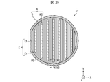
- FIG. 25 is a plan view showing the configuration of the template substrate 7 in Example 6.
- FIG. 26 is a cross-sectional view taken along line XXVI--XXVI shown in FIG. 25.
- FIG. 26 is a cross-sectional view taken along line XXVI--XXVI shown in FIG. 25.
- Example 5 the mask layer 6 was formed after part of the seed layer 3 was removed, but the present invention is not limited to this.
- the seed layer 3 and part of the mask portion 5 may be removed, leaving the end portion 5E of the mask portion 5 and the end portion 3E of the seed layer 3. It may have a protective part PS to cover.
- Example 6 there is a gap D2 between the outer edge 5E of the template substrate 7 in the mask portion 5 and the edge E of the main substrate 1, and the seed Between the edge 3E of the layer 3 and the edge E of the main substrate 1 there may be a distance D3.
- the distance D2 and the distance D3 may be the same or substantially the same.
- the interval D2 and the interval D3 may be different from each other.
- Example 6 for example, first, a base substrate UK is prepared.
- the seed layer 3 is formed on the entire surface of the buffer layer 2 of the base substrate UK, after removing a part of the seed layer 3 by etching or the like so as to have a space D3, a mask layer 6 is formed so as to have a space D2. may be formed.
- the seed layer 3 may be formed to have the interval D3, and then the mask layer 6 may be formed to have the interval D2.
- the seed layer 3 and part of the mask portion 5 may be removed.
- the sixth embodiment has the same effect as the fifth embodiment described above, and when the ELO semiconductor layer 8 is formed on the template substrate 7, the ELO semiconductor layer 8 laterally grown in the Y direction is not formed on the protective portion PS. can be formed. That is, the ELO semiconductor layer 8 does not contact the buffer layer 2 . Therefore, in Example 6, the possibility of occurrence of meltback etching SMB can be further reduced.
- FIG. 27 is a plan view showing the structure of the template substrate 7 in Example 7.
- FIG. 28 is a cross-sectional view taken along line XXVIII--XXVIII shown in FIG. 27.
- Example 6 the protective portion PS, which is a member separate from each layer of the base substrate UK, was formed on the outer periphery of the template substrate 7, but the present invention is not limited to this.
- the protection part PS may be included in the buffer layer 2 .
- Example 7 has the same mask layer 6 and seed layer 3 as in Example 6 described above, and the buffer layer 2 may be used as the protective portion PS. That is, the buffer layer 2 may include the protection portion PS, and the buffer layer 2 and the protection portion PS may be integrated with each other.
- the buffer layer 2 may contain, for example, at least one of an aluminum nitride film and a silicon carbide film, and may be a multilayer film.
- Example 7 the seed layer 3 does not exist on the side surface portion SP of the base substrate UK as in Example 5 described above. An edge E of the main substrate 1 is covered with the buffer layer 2 at the side surface portion SP of the base substrate UK. Even if the buffer layer 2 has an abnormal portion DP such as a crack or a thinned portion, the following can be said. That is, since the seed layer 3 is not in contact with the abnormal portion DP, there is no cause for reaction between the seed layer 3 and the main substrate 1 at the abnormal portion DP. Further, when the ELO semiconductor layer 8 is formed on the template substrate 7, the buffer layer 2 is made of a material having poor reactivity with Ga. Selectively supplied to the part. Therefore, it is possible to reduce the possibility that Ga is supplied to the abnormal portion DP to cause meltback etching SMB.
- an abnormal portion DP such as a crack or a thinned portion
- FIG. 29 is a cross-sectional view showing the configuration of the template substrate 7 in Example 8. As shown in FIG.
- an opening KS and a mask portion 5 are formed by etching or the like on a surface treatment film formed by thermally oxidizing the main substrate 1 or nitriding the main substrate 1.
- the mask portion 5 including the protective portion PS can be formed. That is, the mask portion 5 may be made of the processed film of the main substrate 1 .
- Example 8 for example, first, the main substrate 1 is thermally oxidized or nitrided to form a substrate processing film (thermally oxidized film or nitriding film) as the mask portion 5 of the mask layer 6 . Then, after applying a resist onto the substrate processing film, an opening is formed in the resist by patterning the resist by photolithography. Then, the opening KS is formed by etching the substrate processing film with an etchant such as hydrofluoric acid. Next, while leaving the resist, the underlying layer 4 is formed inside the opening KS using a sputtering method or the like. Thus, the template substrate 7 of Example 8 can be manufactured.
- a substrate processing film thermally oxidized film or nitriding film
- Example 8 the edge E of the main substrate 1 does not have the seed layer 3 and the edge E of the main substrate 1 is covered with the mask portion 5 . Therefore, the possibility of occurrence of meltback etching SMB can be effectively reduced.
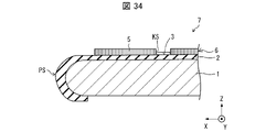
- FIG. 30 is a cross-sectional view showing the configuration of the template substrate 7 in Example 9. As shown in FIG.
- the mask portion 5, which is a substrate processing film, covering the edge E of the main substrate 1 is provided, but the present invention is not limited to this.
- the mask portion 5 is formed by plasma CVD or the like, and the underlying layer 4 may not be formed on the entire main surface 1a of the main substrate 1 .
- Example 9 for example, a silicon oxide film is formed on the entire main surface 1a of the main substrate 1, and after that, similarly to Example 8 described above, after forming an opening KS, a lower portion is formed inside the opening KS. A stratum 4 may be formed.
- the edge E of the main substrate 1 does not have the seed layer 3 and the edge E of the main substrate 1 is covered with the mask portion 5 . Therefore, the possibility of occurrence of meltback etching SMB can be effectively reduced.
- FIG. 31 is a cross-sectional view showing the configuration of the template substrate 7 according to the tenth embodiment.
- Example 5 the configuration was such that the seed layer 3 did not exist on the side surface portion SP of the base substrate UK, but the present invention is not limited to this.
- Example 10 both the buffer layer 2 and the seed layer 3 are not present on the side surface portion SP of the underlying substrate UK, and the mask layer 6 is formed in such a shape that the mask portions 5 are present at both longitudinal ends of the opening KS. can be
- the template substrate 7 in Example 10 has a main substrate 1, an underlying layer 4, and a mask layer 6.
- the mask layer 6 has a mask portion 5 including a protective portion PS. are doing.
- the opening KS has a longitudinal shape, and in plan view, a distance D1 is provided between the tip KE of the opening KS and the edge E of the main substrate 1 (in other words, the position of the ridge line RH described above). may have.
- the tenth embodiment there may be a distance D3 (see the fifth embodiment) between the end portion 3E of the seed layer 3 and the edge E of the main substrate 1. Moreover, you may have the space
- the interval D4 may be smaller than the interval D1.
- the interval D4 may be, for example, 1 ⁇ m or more and 6000 ⁇ m or less.
- the distance D3 and the distance D4 may be the same or substantially the same.
- the interval D3 and the interval D4 may be different from each other.
- Example 10 for example, first, a base substrate UK is prepared.
- a portion of the seed layer 3 may be removed by etching or the like so as to have the spacing D3.
- a portion of the buffer layer 2 may be removed by etching or the like so as to have the interval D4.
- a specific method is not particularly limited as long as the underlying substrate UK from which the seed layer 3 and the buffer layer 2 are partially removed can be obtained.
- the mask layer 6 may be formed so as to have the interval D1 in the same manner as in Example 3 described above. At this time, by forming the mask layer 6 so that the interval D1 is larger than the interval D3 and larger than the interval D4, the main substrate 1 can be prevented from being exposed.
- Example 10 the seed layer 3 and the buffer layer 2 do not exist at the side surface portion SP of the base substrate UK, and the edge E of the main substrate 1 is covered with the protective portion PS that is part of the mask portion 5 . Therefore, the possibility that an abnormal portion DP exists in the side surface portion SP of the base substrate UK is reduced, and the possibility that Ga in the atmosphere reaches the main substrate 1 and reacts during the film formation of the ELO semiconductor layer 8 is reduced. can be reduced. As a result, the possibility of occurrence of meltback etching SMB can be reduced.
- FIG. 32 is a cross-sectional view showing the configuration of the template substrate 7 in Example 11. As shown in FIG.
- the base substrate UK has a configuration in which the buffer layer 2 and the seed layer 3 are provided in order from the main substrate 1 side as the base layer 4, but the configuration is not limited to this. In one embodiment of the present disclosure, no buffer layer 2 may be provided between the main substrate 1 and the seed layer 3 .
- Example 11 the seed layer 3 is provided without the buffer layer 2 , and the underlying substrate UK includes the main substrate 1 and the seed layer 3 .
- a mask layer 6 is formed on the underlying substrate UK.
- the mask layer 6 has a mask portion 5 including a protective portion PS.
- the protective portion PS and the mask portion 5 may be integrated with each other.
- the seed layer 3 may be made of a material that has low reactivity with the main substrate 1 and that can serve as a growth starting point for the ELO semiconductor layer 8 .
- Seed layer 3 may be, for example, an AlN layer or a SiC layer, or a layer containing at least one of AlN and SiC.
- the seed layer 3 may be a single layer film or a multilayer film.
- the seed layer 3 may have a graded structure in which the Al composition changes stepwise, such as an AlN film on the side closer to the main substrate 1 and a GaN film or AlGaN film on the side farther from the main substrate 1. good.
- Example 11 if the seed layer 3 is not sufficiently formed on the edge E of the main substrate 1, an abnormal portion DP may be formed in the seed layer 3 at the side surface portion SP of the base substrate UK.
- the seed layer 3 can be a Ga-free or substantially Ga-free layer, and the seed layer 3 is covered with a protective portion PS at the side portion SP of the base substrate UK. Therefore, it is possible to reduce the possibility of reaction between the main substrate 1 containing silicon and Ga at the abnormal portion DP. Further, even if a reaction occurs in the abnormal portion DP in the seed layer 3, the new supply of Ga to the reaction portion is reduced by the protective portion PS. As a result, the possibility of occurrence of meltback etching SMB can be effectively reduced.
- FIG. 33 is a cross-sectional view showing another configuration of the template substrate 7 in the eleventh embodiment.
- the seed layer 3 may be positioned on the main substrate 1, and the end portion of the seed layer 3 (the portion covering the side surface of the main substrate 1) may function as the protective portion PS.
- the seed layer 3 in this case, a single layer film or a multilayer film containing at least one of AlN and SiC can be used.
- the thickness of the portion (protective portion PS) covering the side surface of the main substrate 1 may be set to be equal to or greater than the thickness of the portion covering the upper surface of the main substrate 1, and the seed layer 3 may extend to the lower surface of the main substrate 1. You can stay.
- FIG. 34 is a cross-sectional view showing the configuration of the template substrate 7 in Example 12.
- the buffer layer 2 is positioned on the main substrate 1, the seed layer 3 is locally provided on the buffer layer 2 so as to overlap with the opening KS of the mask 6, and the edge of the buffer layer 2 is provided.
- the part (the part covering the side surface of the main substrate 1) may be configured to function as the protective part PS.
- a single layer film or a multilayer film containing at least one of AlN and SiC can be used as the buffer layer 2 in this case.
- the thickness of the portion (protective portion PS) covering the side surface of the main substrate 1 may be set to be equal to or greater than the thickness of the portion covering the upper surface of the main substrate 1, and the buffer layer 2 may extend around the lower surface of the main substrate 1. You can stay.
- main substrate 1a main surface 1b lower surface 2 buffer layer (buffer portion) 3 seed layer (seed part) 3E, 5E end 4 base layer (base part) 5 mask part 6 mask layer (mask) 7 template substrate 8 ELO semiconductor layer (ELO semiconductor part) 9 Functional layer (functional part) 10 semiconductor substrate 20 semiconductor device 23 drive substrate 25 control circuit 30 electronic device 70 manufacturing apparatus 71 mask layer forming portion 72 protective portion forming portion 73 semiconductor layer forming portion 74 control portion D1, D2, D3, D4 interval E edge (side surface) Ef Plane portion Er Curved surface portion KS Opening portion PS Protective portion PS1 Lower protective portion
Landscapes
- Chemical & Material Sciences (AREA)
- General Physics & Mathematics (AREA)
- Physics & Mathematics (AREA)
- Organic Chemistry (AREA)
- Engineering & Computer Science (AREA)
- Crystallography & Structural Chemistry (AREA)
- Materials Engineering (AREA)
- Metallurgy (AREA)
- Inorganic Chemistry (AREA)
- Chemical Kinetics & Catalysis (AREA)
- General Chemical & Material Sciences (AREA)
- Recrystallisation Techniques (AREA)
- Crystals, And After-Treatments Of Crystals (AREA)
Priority Applications (3)
| Application Number | Priority Date | Filing Date | Title |
|---|---|---|---|
| JP2023536693A JPWO2023002865A1 (https=) | 2021-07-21 | 2022-07-08 | |
| US18/580,803 US20250093766A1 (en) | 2021-07-21 | 2022-07-08 | Template substrate and manufacturing method and manufacturing apparatus thereof, semiconductor substrate and manufacturing method and manufacturing apparatus thereof, semiconductor device, and electronic device |
| CN202280050905.2A CN117769613A (zh) | 2021-07-21 | 2022-07-08 | 模板基板和其制造方法以及制造装置、半导体基板和其制造方法以及制造装置、半导体器件、电子设备 |
Applications Claiming Priority (2)
| Application Number | Priority Date | Filing Date | Title |
|---|---|---|---|
| JP2021120981 | 2021-07-21 | ||
| JP2021-120981 | 2021-07-21 |
Publications (1)
| Publication Number | Publication Date |
|---|---|
| WO2023002865A1 true WO2023002865A1 (ja) | 2023-01-26 |
Family
ID=84979204
Family Applications (1)
| Application Number | Title | Priority Date | Filing Date |
|---|---|---|---|
| PCT/JP2022/027064 Ceased WO2023002865A1 (ja) | 2021-07-21 | 2022-07-08 | テンプレート基板並びにその製造方法および製造装置、半導体基板並びにその製造方法および製造装置、半導体デバイス、電子機器 |
Country Status (5)
| Country | Link |
|---|---|
| US (1) | US20250093766A1 (https=) |
| JP (1) | JPWO2023002865A1 (https=) |
| CN (1) | CN117769613A (https=) |
| TW (1) | TWI845987B (https=) |
| WO (1) | WO2023002865A1 (https=) |
Citations (3)
| Publication number | Priority date | Publication date | Assignee | Title |
|---|---|---|---|---|
| JP2007246289A (ja) * | 2004-03-11 | 2007-09-27 | Nec Corp | 窒化ガリウム系半導体基板の作製方法 |
| JP2009256154A (ja) * | 2008-04-21 | 2009-11-05 | Nippon Telegr & Teleph Corp <Ntt> | 半導体結晶成長用基板および半導体結晶 |
| JP2012114263A (ja) * | 2010-11-25 | 2012-06-14 | Pawdec:Kk | 半導体素子およびその製造方法 |
Family Cites Families (4)
| Publication number | Priority date | Publication date | Assignee | Title |
|---|---|---|---|---|
| CN103388178B (zh) * | 2013-08-07 | 2016-12-28 | 厦门市三安光电科技有限公司 | Iii族氮化物外延结构及其生长方法 |
| JP6185398B2 (ja) * | 2014-01-31 | 2017-08-23 | 東京エレクトロン株式会社 | 窒化ガリウム系結晶の成長方法及び熱処理装置 |
| JP6553765B1 (ja) * | 2018-03-20 | 2019-07-31 | 株式会社サイオクス | 結晶基板の製造方法および結晶基板 |
| EP4053881B1 (en) * | 2019-10-29 | 2024-10-09 | Kyocera Corporation | Semiconductor element and method for producing semiconductor element |
-
2022
- 2022-07-08 CN CN202280050905.2A patent/CN117769613A/zh active Pending
- 2022-07-08 JP JP2023536693A patent/JPWO2023002865A1/ja active Pending
- 2022-07-08 WO PCT/JP2022/027064 patent/WO2023002865A1/ja not_active Ceased
- 2022-07-08 US US18/580,803 patent/US20250093766A1/en active Pending
- 2022-07-18 TW TW111126867A patent/TWI845987B/zh active
Patent Citations (3)
| Publication number | Priority date | Publication date | Assignee | Title |
|---|---|---|---|---|
| JP2007246289A (ja) * | 2004-03-11 | 2007-09-27 | Nec Corp | 窒化ガリウム系半導体基板の作製方法 |
| JP2009256154A (ja) * | 2008-04-21 | 2009-11-05 | Nippon Telegr & Teleph Corp <Ntt> | 半導体結晶成長用基板および半導体結晶 |
| JP2012114263A (ja) * | 2010-11-25 | 2012-06-14 | Pawdec:Kk | 半導体素子およびその製造方法 |
Also Published As
| Publication number | Publication date |
|---|---|
| TW202319600A (zh) | 2023-05-16 |
| TWI845987B (zh) | 2024-06-21 |
| JPWO2023002865A1 (https=) | 2023-01-26 |
| US20250093766A1 (en) | 2025-03-20 |
| CN117769613A (zh) | 2024-03-26 |
Similar Documents
| Publication | Publication Date | Title |
|---|---|---|
| JP7817190B2 (ja) | 半導体基板、半導体デバイス、電子機器 | |
| US20240136181A1 (en) | Semiconductor substrate, method for manufacturing the same, apparatus for manufacturing the same, and template substrate | |
| US20100244100A1 (en) | Compound semiconductor substrate | |
| JP7343607B2 (ja) | 半導体素子および半導体素子の製造方法 | |
| JP7776330B2 (ja) | エピタキシャル横方向過成長を用いた非極性及び半極性デバイス作成方法 | |
| EP2858094A1 (en) | Semiconductor laminate structure and semiconductor element | |
| TWI907965B (zh) | 半導體裝置之製造方法及製造裝置 | |
| JP7779906B2 (ja) | 半導体基板並びにその製造方法および製造装置、GaN系結晶体、半導体デバイス、電子機器 | |
| JP2025138740A (ja) | 半導体基板、半導体デバイスの製造方法 | |
| WO2023002865A1 (ja) | テンプレート基板並びにその製造方法および製造装置、半導体基板並びにその製造方法および製造装置、半導体デバイス、電子機器 | |
| JP7828879B2 (ja) | 半導体基板およびその製造方法 | |
| US20130214282A1 (en) | Iii-n on silicon using nano structured interface layer | |
| JP7634076B2 (ja) | テンプレート基板並びにその製造方法および製造装置、半導体基板並びにその製造方法および製造装置 | |
| US20240313151A1 (en) | Semiconductor device manufacturing method and manufacturing apparatus, semiconductor device and electronic device | |
| US20160013275A1 (en) | Iii-nitride semiconductor stacked structure | |
| WO2025063259A1 (ja) | テンプレート基板およびその製造方法、半導体基板およびその製造方法、テンプレート基板の製造装置並びに半導体デバイスの製造方法 |
Legal Events
| Date | Code | Title | Description |
|---|---|---|---|
| 121 | Ep: the epo has been informed by wipo that ep was designated in this application |
Ref document number: 22845799 Country of ref document: EP Kind code of ref document: A1 |
|
| WWE | Wipo information: entry into national phase |
Ref document number: 202280050905.2 Country of ref document: CN |
|
| WWE | Wipo information: entry into national phase |
Ref document number: 18580803 Country of ref document: US Ref document number: 2023536693 Country of ref document: JP |
|
| NENP | Non-entry into the national phase |
Ref country code: DE |
|
| 122 | Ep: pct application non-entry in european phase |
Ref document number: 22845799 Country of ref document: EP Kind code of ref document: A1 |
|
| WWP | Wipo information: published in national office |
Ref document number: 18580803 Country of ref document: US |