WO2023002709A1 - 荷重検出システム - Google Patents
荷重検出システム Download PDFInfo
- Publication number
- WO2023002709A1 WO2023002709A1 PCT/JP2022/014161 JP2022014161W WO2023002709A1 WO 2023002709 A1 WO2023002709 A1 WO 2023002709A1 JP 2022014161 W JP2022014161 W JP 2022014161W WO 2023002709 A1 WO2023002709 A1 WO 2023002709A1
- Authority
- WO
- WIPO (PCT)
- Prior art keywords
- load
- microcomputer
- detection circuit
- detection
- signal
- Prior art date
- Legal status (The legal status is an assumption and is not a legal conclusion. Google has not performed a legal analysis and makes no representation as to the accuracy of the status listed.)
- Ceased
Links
Images





Classifications
-
- G—PHYSICS
- G01—MEASURING; TESTING
- G01L—MEASURING FORCE, STRESS, TORQUE, WORK, MECHANICAL POWER, MECHANICAL EFFICIENCY, OR FLUID PRESSURE
- G01L1/00—Measuring force or stress, in general
- G01L1/14—Measuring force or stress, in general by measuring variations in capacitance or inductance of electrical elements, e.g. by measuring variations of frequency of electrical oscillators
- G01L1/142—Measuring force or stress, in general by measuring variations in capacitance or inductance of electrical elements, e.g. by measuring variations of frequency of electrical oscillators using capacitors
- G01L1/144—Measuring force or stress, in general by measuring variations in capacitance or inductance of electrical elements, e.g. by measuring variations of frequency of electrical oscillators using capacitors with associated circuitry
-
- G—PHYSICS
- G01—MEASURING; TESTING
- G01L—MEASURING FORCE, STRESS, TORQUE, WORK, MECHANICAL POWER, MECHANICAL EFFICIENCY, OR FLUID PRESSURE
- G01L1/00—Measuring force or stress, in general
- G01L1/14—Measuring force or stress, in general by measuring variations in capacitance or inductance of electrical elements, e.g. by measuring variations of frequency of electrical oscillators
- G01L1/142—Measuring force or stress, in general by measuring variations in capacitance or inductance of electrical elements, e.g. by measuring variations of frequency of electrical oscillators using capacitors
- G01L1/146—Measuring force or stress, in general by measuring variations in capacitance or inductance of electrical elements, e.g. by measuring variations of frequency of electrical oscillators using capacitors for measuring force distributions, e.g. using force arrays
Definitions
- the present invention relates to a load detection system with multiple load sensors.
- Load sensors are widely used in fields such as industrial equipment, robots and vehicles. 2. Description of the Related Art In recent years, along with the development of computer control technology and the improvement of design, the development of electronic devices such as humanoid robots and interior parts of automobiles that use free-form surfaces in various ways is progressing. Accordingly, it is required to mount high-performance load sensors on each free-form surface.
- Patent Document 1 describes a load sensor that detects an externally applied load based on a change in capacitance.
- this load sensor a plurality of element portions each capable of individually detecting a load are arranged adjacent to each other in the planar direction. During load detection, the element units to be detected are switched in order. A capacitance that changes according to the load is acquired as a voltage generated in each element portion.
- a detection circuit for detecting the voltage change of the element portion according to the load is provided individually for each load sensor. Furthermore, each detection circuit is connected to a host circuit that controls the system. For example, a common power supply and ground is applied to each detection circuit and higher level circuitry. As a result, these detection circuits and upper circuits are integrated into one circuit system.
- an object of the present invention is to provide a load detection system capable of suppressing noise generated from one load sensor detection circuit from affecting load detection in other detection circuits.
- a load detection system includes a first load sensor including a first element unit whose capacitance changes according to a load; A first detection circuit that acquires a voltage corresponding to the capacitance at a detection timing within a period; a second load sensor that includes a second element unit whose capacitance changes according to a load; and the second element. a second detection circuit that charges and discharges the unit and acquires a voltage corresponding to the capacitance at a detection timing within a charging period; charging the first element unit and charging the second element unit; and a synchronization generator for synchronizing the
- the first detection circuit and the second detection circuit large noise is likely to occur when discharging to each element unit. Therefore, when a voltage is acquired by the other detection circuit while discharging is being performed in one of the detection circuits, the acquired voltage is affected by noise from the one detection circuit.
- the load detection system since the charging of the first element unit and the charging of the second element unit are synchronized, the discharge period for one element unit corresponds to the detection timing for the other element unit. overlap is avoided. Therefore, it is possible to suppress the voltage acquired by the other detection circuit from being affected by noise from the one detection circuit. Therefore, it is possible to accurately measure the load applied to each element portion of the first load sensor and the second load sensor.
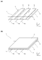
- FIG. 1(a) is a perspective view schematically showing a sheet-like member and a conductive elastic body placed on a facing surface of the sheet-like member according to Embodiment 1.
- FIG. 1(b) is a perspective view schematically showing a state in which conductor wires are installed in the structure of FIG. 1(a) according to the first embodiment.
- 2(a) is a perspective view schematically showing a state in which threads are installed in the structure of FIG. 1(b) according to Embodiment 1.
- FIG. 2(b) is a perspective view schematically showing a state in which a sheet-like member is installed on the structure of FIG. 2(a) according to Embodiment 1.
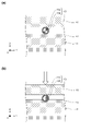
- FIG. 3A and 3B are diagrams schematically showing cross sections of a conductive elastic body and a conductor wire, respectively, according to Embodiment 1.
- FIG. 4 is a plan view schematically showing the internal configuration of the load sensor according to the first embodiment;
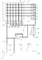
- FIG. 5 is a circuit diagram showing a configuration of a detection circuit according to the first embodiment;
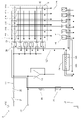
- FIG. 6 is a circuit diagram schematically showing states of a load sensor and a detection circuit during charging according to the first embodiment;
- FIG. 7 is a circuit diagram schematically showing states of a load sensor and a detection circuit during discharge according to the first embodiment;
- FIG. FIG. 8 is a block diagram showing the configuration of the load detection system according to the first embodiment.
- FIG. 9 is a diagram schematically showing configurations of a plurality of detection circuits and a system-side microcomputer, and transmission and reception of signals, according to the first embodiment;
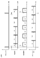
- FIG. FIG. 10 is a timing chart showing states of a synchronization signal, a measurement signal, a charge/discharge signal, a count-up signal, and a potential signal output from the signal processing circuit to the microcomputer in each detection circuit according to the first embodiment.
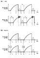
- FIG. 11A is a graph schematically showing a potential signal acquired by a detection circuit according to a comparative example.
- FIG. 11(b) is a graph schematically showing potential signals obtained by the detection circuit according to the first embodiment.
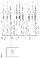
- FIG. 12 is a diagram schematically showing configurations of a plurality of detection circuits and a system-side microcomputer, and transmission and reception of signals, according to the second embodiment
- FIG. 13 is a diagram schematically showing configurations of a plurality of detection circuits and a system-side microcomputer, and transmission and reception of signals, according to the third embodiment
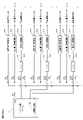
- FIG. 14 is a diagram schematically showing configurations of a plurality of detection circuits and a system-side microcomputer, and transmission and reception of signals, according to the fourth embodiment.
- FIG. 15 is a time chart showing states of a synchronization signal, a measurement signal, a charge/discharge signal, and a count-up signal according to the modification.
- the load detection system according to the present invention can be applied to a management system or the like that performs processing according to the applied load.
- multiple load sensors may be used, for example, to detect loads over a wider range.
- management systems include inventory management systems, driver monitoring systems, coaching management systems, security management systems, nursing care and childcare management systems.
- a load sensor installed on the inventory shelf detects the load of the loaded inventory, and detects the type and number of products on the inventory shelf.
- a load sensor provided in the refrigerator detects the load of the food in the refrigerator, and detects the type of food in the refrigerator and the number and amount of the food. As a result, it is possible to automatically propose a menu using the food in the refrigerator.
- a load sensor provided in the steering device monitors the driver's load distribution on the steering device (eg gripping force, gripping position, pedaling force).
- a load sensor provided on the vehicle seat monitors the load distribution (for example, the position of the center of gravity) of the driver on the vehicle seat while the driver is seated. As a result, the driver's driving state (drowsiness, psychological state, etc.) can be fed back.
- the load distribution on the soles of the feet is monitored by load sensors provided on the soles of the shoes. As a result, it is possible to correct or guide the user to an appropriate walking state or running state.
- a load sensor installed on the floor detects the load distribution when a person passes through, and detects the weight, stride length, passing speed, shoe sole pattern, and so on. This makes it possible to identify a passing person by collating this detection information with the data.
- load sensors installed on bedding and toilet seats monitor the load distribution of the human body on bedding and toilet seats. As a result, it is possible to estimate what kind of action the person is trying to take at the position of the bedding and toilet seat, and prevent overturning and falling.
- a load detection system includes a plurality of load sensors for detecting loads, and a detection circuit provided for each load sensor.
- the load sensors of the following embodiments are capacitive load sensors. Such a load sensor may also be called a "capacitive pressure sensor element", a “capacitive pressure detection sensor element”, a “pressure sensitive switch element”, or the like.
- the following embodiment is one embodiment of the present invention, and the present invention is not limited to the following embodiment.
- the Z-axis direction is the height direction of the load sensor 1 .
- FIG. 1(a) is a perspective view schematically showing the sheet-like member 11 and the conductive elastic body 12 installed on the facing surface (the surface on the Z-axis positive side) of the sheet-like member 11.
- FIG. 1(a) is a perspective view schematically showing the sheet-like member 11 and the conductive elastic body 12 installed on the facing surface (the surface on the Z-axis positive side) of the sheet-like member 11.
- the sheet member 11 is an elastic insulating member, and has a flat plate shape parallel to the XY plane.
- the thickness of the sheet member 11 in the Z-axis direction is, for example, 0.01 mm to 2 mm.
- the sheet member 11 is made of a non-conductive resin material or a non-conductive rubber material.
- the resin material used for the sheet member 11 is selected from the group consisting of, for example, styrene-based resins, silicone-based resins (eg, polydimethylpolysiloxane (PDMS), etc.), acrylic-based resins, rotaxane-based resins, and urethane-based resins. At least one selected resin material.
- Rubber materials used for the sheet member 11 include, for example, silicone rubber, isoprene rubber, butadiene rubber, styrene-butadiene rubber, chloroprene rubber, nitrile rubber, polyisobutylene, ethylene-propylene rubber, chlorosulfonated polyethylene, acrylic rubber, and fluororubber. , epichlorohydrin rubber, urethane rubber, and natural rubber.
- the conductive elastic body 12 is formed on the facing surface of the sheet member 11 (surface on the Z-axis positive side).
- three conductive elastic bodies 12 are formed on the facing surface of a sheet member 11 .
- the conductive elastic body 12 is a conductive member having elasticity.
- Each conductive elastic body 12 has a belt-like shape that is long in the Y-axis direction, and is arranged side by side in the X-axis direction at predetermined intervals.
- a cable 12 a electrically connected to the conductive elastic body 12 is installed at the Y-axis negative side end of each conductive elastic body 12 .
- the conductive elastic body 12 is formed on the opposing surface of the sheet member 11 by a printing method such as screen printing, gravure printing, flexographic printing, offset printing, and gravure offset printing. According to these printing methods, it is possible to form the conductive elastic body 12 on the facing surface of the sheet member 11 with a thickness of about 0.001 mm to 0.5 mm.
- the conductive elastic body 12 is composed of a resin material and conductive filler dispersed therein, or a rubber material and conductive filler dispersed therein.
- the resin material used for the conductive elastic body 12 is similar to the resin material used for the sheet-shaped member 11 described above, and may be, for example, a styrene resin, a silicone resin (polydimethylpolysiloxane (eg, PDMS), etc.), or an acrylic resin. , rotaxane-based resins, urethane-based resins, and the like.
- the rubber material used for the conductive elastic body 12 is the same as the rubber material used for the sheet member 11 described above, for example, silicone rubber, isoprene rubber, butadiene rubber, styrene-butadiene rubber, chloroprene rubber, nitrile rubber, polyisobutylene, At least one rubber material selected from the group consisting of ethylene propylene rubber, chlorosulfonated polyethylene, acrylic rubber, fluororubber, epichlorohydrin rubber, urethane rubber, natural rubber, and the like.
- Conductive fillers used for the conductive elastic body 12 include, for example, Au (gold), Ag (silver), Cu (copper), C (carbon), ZnO (zinc oxide), In 2 O 3 (indium oxide (III) ), and metal materials such as SnO 2 (tin (IV) oxide), and PEDOT:PSS (that is, a composite of poly(3,4-ethylenedioxythiophene) (PEDOT) and polystyrene sulfonic acid (PSS)). It is at least one material selected from the group consisting of conductive polymer materials such as metal-coated organic fibers and metal wires (fiber state).
- FIG. 1(b) is a perspective view schematically showing a state in which conductor wires 13 are installed in the structure of FIG. 1(a).
- the conductor wire 13 has a linear shape and is arranged so as to overlap the upper surface of the conductive elastic body 12 shown in FIG. 1(a).
- three conductor wires 13 are arranged to overlap the upper surfaces of three conductive elastic bodies 12 .
- the three conductor wires 13 are arranged side by side at predetermined intervals along the longitudinal direction (Y-axis direction) of the conductive elastic body 12 so as to intersect the conductive elastic body 12 .
- Each conductor line 13 is arranged extending in the X-axis direction so as to straddle three conductive elastic bodies 12 .
- Conductor wire 13 is, for example, a coated copper wire.
- the conductor line 13 is composed of a linear conductive member and a dielectric formed on the surface of the conductive member. The configuration of the conductor wire 13 will be described later with reference to FIGS. 3(a) and 3(b).
- FIG. 2(a) is a perspective view schematically showing a state in which the thread 14 is installed in the structure of FIG. 1(b).
- each conductor wire 13 is connected to the sheet member 11 by a thread 14 so as to be movable in the longitudinal direction (X-axis direction) of the conductor wires 13. .
- 12 threads 14 connect the conductor wires 13 to the sheet member 11 at positions other than the position where the conductive elastic body 12 and the conductor wires 13 overlap.
- the thread 14 is composed of chemical fibers, natural fibers, mixed fibers thereof, or the like.
- FIG. 2(b) is a perspective view schematically showing a state in which the sheet-like member 15 is installed on the structure of FIG. 2(a).
- a sheet-like member 15 is installed from above (Z-axis positive side) of the structure shown in FIG. 2(a).
- the sheet member 15 is an insulating member.
- Sheet member 15 is, for example, at least one resin material selected from the group consisting of polyethylene terephthalate, polycarbonate, polyimide, and the like.
- the sheet-like member 15 has a flat plate shape parallel to the XY plane, and has the same size and shape as the sheet-like member 11 in plan view.
- the thickness of the sheet member 15 in the Z-axis direction is, for example, 0.01 mm to 2 mm.
- the sheet-shaped member 11 and the sheet-shaped member 15 are fixed by connecting the four peripheral sides of the sheet-shaped member 15 to the four peripheral sides of the sheet-shaped member 11 with a silicone rubber adhesive, thread, or the like. Thereby, the conductor wire 13 is sandwiched between the conductive elastic body 12 and the sheet member 15 . Thus, the load sensor 1 is completed as shown in FIG. 2(b).
- FIG. 3A and 3B schematically show cross sections of the conductive elastic body 12 and the conductor wire 13 when cut along a plane parallel to the YZ plane at the center position of the conductive elastic body 12 in the X-axis direction.
- FIG. 4 is a diagram showing; FIG. 3(a) shows a state in which no load is applied, and FIG. 3(b) shows a state in which a load is applied.
- FIGS. 3A and 3B the surface of the sheet-like member 11 on the Z-axis negative side is installed on the installation surface.
- the conductor wire 13 is composed of a conductive member 13a and a dielectric 13b formed on the conductive member 13a.
- the conductive member 13a is a wire having a linear shape, and the dielectric 13b covers the surface of the conductive member 13a.
- Conductive member 13a is made of copper, for example, and has a diameter of approximately 60 ⁇ m, for example.
- Dielectric 13b has electrical insulation and is made of, for example, a resin material, a ceramic material, or a metal oxide material.
- Dielectric 13b is at least one selected from the group consisting of polypropylene resin, polyester resin (eg, polyethylene terephthalate resin), polyimide resin, polyphenylene sulfide resin, polyvinyl formal resin, polyurethane resin, polyamideimide resin, polyamide resin, and the like.
- a resin material may be used, or at least one metal oxide material selected from the group consisting of Al 2 O 3 and Ta 2 O 5 may be used.
- FIG. 4 is a plan view schematically showing the internal configuration of the load sensor 1.
- FIG. 4 illustration of the thread 14 and the sheet-like member 15 is omitted for the sake of convenience.
- element portions A11, A12, A13, A21, A22, A23, and A31 whose capacitance changes according to the load are placed at the positions where the three conductive elastic bodies 12 and the three conductor wires 13 intersect. , A32 and A33 are formed.
- Each element part includes the conductive elastic body 12 and the conductor wire 13 in the vicinity of the intersection of the conductive elastic body 12 and the conductor wire 13 .
- the conductor wire 13 constitutes one pole of the capacitance (for example, the anode), and the conductive elastic body 12 constitutes the other pole of the capacitance (for example, the cathode). That is, the conductive member 13a (see FIGS. 3A and 3B) in the conductor wire 13 constitutes one electrode of the load sensor 1 (capacitive load sensor), and the conductive elastic body 12 functions as a load sensor.
- the dielectric 13b (see FIGS. 3A and 3B) in the conductor wire 13 constitutes the other electrode of the sensor 1 (capacitive load sensor), and the load sensor 1 (capacitive load sensor ) corresponds to the dielectric that defines the capacitance.
- the conductive members 13a in the three conductor wires 13 are called lines L11, L12, and L13, and the cables 12a pulled out from the three conductive elastic bodies 12 are called lines L21, L22, and L23.
- the positions where the line L11 intersects the conductive elastic body 12 connected to the lines L21, L22, and L23 are the element portions A11, A12, and A13, respectively, and the line L12 is the conductive elastic body connected to the lines L21, L22, and L23.
- 12 are element portions A21, A22, and A23, respectively, and the positions where the line L13 intersects the conductive elastic bodies 12 connected to the lines L21, L22, and L23 are element portions A31, A32, and A33, respectively.
- the load applied to the element portion A11 can be calculated by detecting the capacitance between the line L11 and the line L21.
- the load applied to the other element portion can be calculated by detecting the capacitance between two intersecting lines in the other element portion.
- FIG. 5 is a circuit diagram showing the configuration of the detection circuit 2. As shown in FIG. 5, for the load sensor 1, only the conductor wire 13 and the conductive elastic body 12 are shown for convenience, and the conductive elastic body 12 is shown linearly. Also, in FIG. 5, the number of conductor wires 13 and conductive elastic bodies 12 is six, unlike the examples shown in FIGS.
- the detection circuit 2 includes a switch 21, a resistor 22, an equipotential generation unit 23, switches 24 and 25, a resistor 26, a voltage measurement terminal 27, a first switching unit 30, a second switching unit 40, Prepare.
- the detection circuit 2 is a circuit for detecting a change in capacitance at an intersection position between the conductor wire 13 and the conductive elastic body 12 with respect to the load sensor 1 .
- One terminal of the switch 21 is connected to the VCC power supply line of the load detection system 4 to be described later, and the other terminal of the switch 21 is connected to the resistor 22 .
- a resistor 22 is arranged between the switch 21 and the plurality of conductor lines 13 .
- a downstream terminal of the resistor 22 is connected to the first supply line L1.
- the first supply line L1 is connected to the first switching section 30, the equipotential generating section 23, the resistor 26, and the voltage measurement terminal 27.
- An output terminal of the equipotential generator 23 is connected to the second supply line L2.
- the equipotential generator 23 is an operational amplifier, and the output side terminal and the input side minus terminal are connected to each other.
- the equipotential generator 23 generates a suppression voltage that is equipotential to the potential of the first supply line L1 (potential on the downstream side of the resistor 22).
- the second supply line L2 is connected to the equipotential generating section 23, the first switching section 30 and the second switching section 40.
- the switch 24 is an electric element including a resistance component interposed between the second supply line L2 and the ground line L3.
- the switching function of the switch 24 is shown as a switch portion 24a, and the resistance component of the switch 24 is shown as a resistance portion 24b.
- the switch portion 24a When the switch portion 24a is turned on, the second supply line L2 is connected to the ground line L3 via the resistance portion 24b.
- the switch 25 is interposed between the first supply line L1 and the ground line L3. When the switch 25 is turned on, the first supply line L1 is connected through the resistor 26 to the ground line L3.
- the voltage measurement terminal 27 is connected to a signal processing circuit 113 which will be described later.
- the first switching unit 30 selectively selects one of the first supply line L1 for supplying the downstream potential of the resistor 22 and the second supply line L2 for supplying the suppression voltage. (Conductive member 13a).
- the first switching section 30 includes six multiplexers 31 .
- the six multiplexers 31 are provided corresponding to the six conductor lines 13 (conductive members 13a), respectively.
- a conductive member 13 a of the conductor line 13 is connected to the output terminal of each multiplexer 31 .
- Each multiplexer 31 has two input terminals.
- a first supply line L1 is connected to one input terminal, and a voltage is applied to this input terminal from the VCC power supply line via the first supply line L1 and a resistor 22 .
- the other input terminal of the multiplexer 31 is connected to the second supply line L2, and the suppression voltage is applied to this input terminal from the equipotential generator 23 via the second supply line L2.
- the second switching unit 40 selectively connects one of the second supply line L2 for supplying the inhibition voltage and the ground line L3 set to have the same potential as the ground to the conductive elastic body 12 (cable 12a). .
- the second switching section 40 includes six multiplexers 41 .
- the six multiplexers 41 are provided corresponding to the six conductive elastic bodies 12 (cables 12a), respectively.
- a cable 12 a connected to the conductive elastic body 12 is connected to the output terminal of each multiplexer 41 .
- Each multiplexer 41 has two input terminals.
- a second supply line L2 is connected to one of the input terminals, and a suppression voltage is applied to this input terminal from the equipotential generator 23 via the second supply line L2.
- the other input terminal of the multiplexer 41 is connected to the ground line L3.
- the switching of the switch 21, the switch section 24a, the switch 25, and the multiplexers 31 and 41 is controlled by the microcomputer 110 (see FIG. 9) of the detection circuit 2 as described later.
- the microcomputer 110 (see FIG. 9), as shown below, sequentially performs , to obtain the potential that varies with load.
- the microcomputer 110 controls the multiplexer 31 so that the multiplexer 31 connected to the conductor line 13 (conductive member 13a) constituting the electrode of the element portion A11 is connected to the first supply line L1. switch. Also, the microcomputer 110 switches the other five multiplexers 31 so that the other five multiplexers 31 are connected to the second supply line L2.
- the microcomputer 110 switches the multiplexer 41 so that the multiplexer 41 connected to the conductive elastic body 12 forming the electrode of the element section A11 is connected to the ground line L3. Also, the microcomputer 110 switches the other five multiplexers 41 so that the other five multiplexers 41 are connected to the second supply line L2.
- the microcomputer 110 switches the switch section 24a and the switch 25 to the OFF state.
- the microcomputer 110 turns on the switch 21 for a predetermined period of time to apply the rectangular voltage to the first supply line L1. As a result, charging of the element unit A11 to be measured is started.
- FIG. 6 is a circuit diagram schematically showing the state after the switch 21 is set to the ON state when the element section A11 is the object of measurement.
- the thick line indicates a portion having the same potential as the potential of the first supply line L1.
- the potential from the equipotential generator 23 is applied to the cathode side of the other element portions A12 to A16 in the same row (same conductor line 13) as the element portion A11 to be measured. becomes equipotential. Therefore, since electric charges are not accumulated in the other element portions A12 to A16, electric charges are properly accumulated in the element portion A11 to be measured, and the voltage of the element portion A11 is accurately measured. In addition, since the potential from the equipotential generation unit 23 is applied to the anode and cathode of the other element units in the same row (same conductive elastic body 12) as the element units A12 to A16, these other element units No charge builds up. Therefore, these element portions can be invalidated in the measurement.
- the potential from the equipotential generator 23 is applied to the anode of the other element part in the same row (same conductive elastic body 12) as the element part A11 to be measured, and the ground line L3 is connected to the cathode. Therefore, electric charges are accumulated in these other element portions. However, since the anodes of these element portions are separated from the first supply line L1, the charges accumulated in these other element portions do not affect the measurement of the potential of the element portion A11.
- the switch 21 When the microcomputer 110 acquires the potential of the element unit A11 to be measured, the switch 21 is turned off at a predetermined timing (discharge start timing T3, which will be described later). Then, the microcomputer 110 turns on the switch section 24a so that the second supply line L2 and the ground line L3 are connected, and turns the switch 25 so that the first supply line L1 and the ground line L3 are connected. Switch to ON state. As a result, electric charges accumulated in each element portion are discharged.
- FIG. 7 is a circuit diagram schematically showing a state in which discharge is performed by switching the switch 21, the switch section 24a, and the switch 25 from the state of FIG.
- the conductor line 13 where the element part A11 to be measured is located is connected to the ground line L3 via the resistor 26 and the switch 25.
- the conductor wire 13 different from the conductor wire 13 where the element portion A11 is located and the conductive elastic body 12 same as the conductive elastic body 12 where the element portions A12 to A16 are located are connected to the ground line L3 via the switch 24. be. As a result, electric charges accumulated in all the element portions are discharged.
- the microcomputer 110 sets the connection state of the multiplexers 31 and 41 in order to set the next element unit to be measured, switches the switch unit 24a and the switch 25 to the off state, and turns off the switch 21 as in FIG. Switch to ON state.
- the microcomputer 110 sequentially acquires and stores potentials for the respective element units.
- the microcomputer 110 acquires and stores the potentials of all the element units, it transmits the potential of each element unit to the system-side microcomputer 3 (see FIG. 8).
- FIG. 8 is a block diagram showing the configuration of the load detection system 4. As shown in FIG.
- the load detection system 4 includes a plurality of load sensors 1, a plurality of detection circuits 2 connected to the plurality of load sensors 1, and a system-side microcomputer 3.
- the plurality of load sensors 1 are spread out in the plane direction according to the entire load detection range of the load detection system 4 .
- the plurality of load sensors 1 are arranged in a row in one direction or in a matrix.
- the plurality of load sensors 1 do not necessarily have to be arranged adjacent to each other, and for example, when the load detection ranges of the load detection system 4 are separated, they may be arranged in a state separated from each other.
- the detection circuit 2 includes the circuit system of FIG. 5 and controls the switches of the load sensor 1 and the like. Further, the detection circuit 2 sequentially acquires the potential signal of each element unit through the voltage measurement terminal 27 of the corresponding load sensor 1, and AD-converts the acquired potential signal to generate potential data. The detection circuit 2 transmits the potential data of all the element parts to the system-side microcomputer 3 in response to acquiring the potential signals of all the element parts.
- the system-side microcomputer 3 receives the potential data sent from the plurality of detection circuits 2, and calculates the capacitance of each element of the plurality of load sensors 1 based on the potential, the time constant, and the voltage value of the rectangular voltage. do. Then, the system-side microcomputer 3 calculates the load applied to each element based on the capacitance of each element. In this way, the loads applied to all the element portions of the plurality of load sensors 1 are calculated.
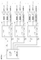
- FIG. 9 is a diagram schematically showing the configuration of a plurality of detection circuits 2 and system-side microcomputer 3, and transmission and reception of signals.
- FIG. 9 shows three detection circuits 2 out of n (n is an integer equal to or greater than 2) detection circuits 2 .
- the detection circuit 2 includes a microcomputer 110, drive circuits 111 and 112, and a signal processing circuit 113 in addition to the circuit system of FIG.
- the microcomputer 110 has an arithmetic processing circuit, and is configured by, for example, an FPGA or MPU.
- the microcomputer 110 has an ADC 110a and a memory 110b.
- the memory 110b stores programs for processing performed by the microcomputer 110, and the like.
- the microcomputer 110 executes various processes according to programs in the memory 110b.
- one microcomputer 110 among the plurality of microcomputers 110 (the uppermost microcomputer 110 in FIG. 9) has a synchronization generator 120 .
- This microcomputer 110 executes the functions of the synchronization generating section 120 according to a program stored in the memory 110b.
- Other microcomputers 110 do not have the synchronization generator 120 .
- the synchronization generator 120 may be included in another microcomputer 110 .
- the drive circuit 111 switches the charge/discharge switch (switch 21, switch section 24a and switch 25 shown in FIG. 5) of the corresponding load sensor 1 according to instructions from the microcomputer 110 .
- the drive circuit 112 switches the corresponding cell selection switch (the first switching section 30 and the second switching section 40 shown in FIG. 5) of the load sensor 1 according to the instruction from the microcomputer 110 .
- the signal processing circuit 113 is connected to the corresponding voltage measurement terminal 27 (see FIG. 5) of the load sensor 1, and amplifies the potential signal from the voltage measurement terminal 27 and removes noise.
- the signal processing circuit 113 has, for example, a capacitor as a configuration for removing noise from the potential signal.
- the ADC 110a converts the analog potential signal V0n input from the corresponding signal processing circuit 113 into digital data.
- the digital potential data converted by the ADC 110a are sequentially stored in the memory 110b.
- the microcomputer 110 transmits the potential data D0n for all the element portions to the system side microcomputer 3.
- the microcomputer 110 of each detection circuit 2 is connected to the system-side microcomputer 3.
- the uppermost microcomputer 110 having the synchronization generator 120 has a port P0 for transmitting a synchronization signal S0, which will be described later, and all the microcomputers 110 have a port P1 to which the synchronization signal S0 is input.
- the system-side microcomputer 3 has an arithmetic processing circuit, and is configured by, for example, an FPGA or MPU.
- the system-side microcomputer 3 calculates the load applied to each element portion of the plurality of load sensors 1 based on the potential data D0n sent from the plurality of detection circuits 2 .
- the microcomputer 110 having the synchronization generation section 120 performs the function of the synchronization generation section 120 to perform and outputs a synchronizing signal S0 for instructing the start of charging to the element portion.
- Each microcomputer 110 starts processing (charging, measuring, discharging, and switching) on the element section, triggered by the input of this synchronization signal S0 to the port P1. Thereby, the processing in each detection circuit 2 is performed in synchronization with each other.
- FIG. 10 is a time chart showing states of the synchronization signal S0, measurement signal, charge/discharge signal, count-up signal, and potential signal V0n output from the signal processing circuit 113 to the microcomputer 110 in each detection circuit 2.
- FIG. The horizontal axis of each graph indicates elapsed time.
- the microcomputer 110 When the microcomputer 110 receives the synchronization signal S0 at the synchronization timing T0, it raises the charge/discharge signal supplied to the drive circuit 111 at the charging start timing T1 after the elapsed time Te1 from the synchronization timing T0. Further, the microcomputer 110 causes the charge/discharge signal to fall at a discharge start timing T3 after the elapsed time Te2 from the charge start timing T1.
- the drive circuit 111 switches the charge/discharge switches (the switch 21, the switch section 24a, and the switch 25 in FIG. 5) according to the charge/discharge signal. Specifically, the drive circuit 111 sets the switch 21 to the ON state at the charging start timing T1, and keeps the switch section 24a and the switch 25 to be OFF. Then, at the discharge start timing T3, the drive circuit 111 sets the switch 21 to the OFF state and sets the switches 24a and 25 to the ON state.
- the microcomputer 110 receives the synchronization signal S0 at the synchronization timing T0, it outputs the measurement signal to the ADC 110a at the measurement timing T2 after the elapsed time Te3 from the synchronization timing T0.
- ADC 110a measures the potential of voltage measurement terminal 27 according to the measurement signal.
- the signal processing circuit 113 constantly amplifies and removes noise from the potential signal from the voltage measurement terminal 27 and outputs the processed potential signal V0n to the microcomputer 110 .
- the ADC 110a converts the potential signal V0n into digital potential data at the measurement timing T2 when the measurement signal is received, and stores the potential data in the memory 110b.
- the microcomputer 110 receives the synchronization signal S0 at the synchronization timing T0, it outputs a count-up signal to the drive circuit 112 at the switching timing T4 after the elapsed time Te4 from the synchronization timing T0.
- the drive circuit 112 increments the counter by 1 in response to the reception of the count-up signal, and operates the cell selection switch (the first switch in FIG. section 30 and the second switching section 40).
- the drive circuit 112 includes a counter that counts count-up signals up to the total number of element units included in the load sensor 1 and returns to 1 when the next count-up signal arrives.
- the initial value of the counter is one.
- the count value of the counter is associated with the cell number of the element section. For example, in the load sensor 1 of FIG. 5, the cell number of the element portion A11 at the upper left corner is 1, and the cell number of the element portion A11 at the lower right corner is 36.
- the drive circuit 112 increments the counter by 1 in response to the reception of the count-up signal, and selects the cell so that the element portion with the next cell number becomes the potential signal measurement target when the next potential signal is measured.
- the switches (the first switching section 30 and the second switching section 40 in FIG. 5) are switched. In this way, at the switching timing T4, preparations for charging and discharging the element portion to be measured next are performed.
- the microcomputer 110 outputs a count-up signal at the switching timing T4 after the discharge period Td has passed after the charge/discharge signal is lowered at the discharge start timing T3.
- the discharge period Td at this time is set slightly longer than the longest discharge period defined by the charge amount that can be charged in the element portion and the resistance portions 24 b and 26 .
- the microcomputer 110 at the top in FIG. 9 outputs the synchronization signal S0 after the elapsed time Te5 from the output of the count-up signal in FIG. All microcomputers 110, upon receiving the synchronization signal S0 output from the microcomputer 110 in the uppermost stage, perform the same measurement processing as described above on the next element section to be measured. That is, every time the microcomputer 110 receives the synchronization signal S0, the microcomputer 110 transmits and receives the above-described signal, and performs processing on the device to be measured. Then, according to the count-up signal, the element section to be measured is changed to the next element section. After that, when the microcomputer 110 receives the synchronizing signal S0, it processes the next element section in the same manner as described above.
- the microcomputer 110 transmits the measured values of all the element parts stored in the memory 110b to the system side microcomputer 3 as potential data D0n (see FIG. 9). do. After that, the microcomputer 110 changes the measurement target to the first element section, and performs measurement of each element section in the same manner as described above.
- FIG. 11(a) is a graph schematically showing the potential signal V0n acquired by the detection circuit 2 according to the comparative example.
- FIG. 11(b) is a graph schematically showing the potential signal V0n obtained by the detection circuit 2 according to the first embodiment.
- 11A and 11B show the potential signal V0n of one detection circuit 2 (first detection circuit) and the other detection circuit (second detection circuit) among the plurality of detection circuits 2.
- the microcomputer 110 of the first detection circuit and the microcomputer 110 of the second detection circuit each perform load detection processing for the load sensor 1 in response to a measurement start instruction from the system-side microcomputer 3 after the load detection system 4 is activated. to start.
- each microcomputer 110 sets the charging start timing T1 of the next measurement cycle to the timing when a predetermined time Tw has passed from the switching timing T4, and performs the measurement processing for the next element unit.
- each microcomputer 110 of the first detection circuit and the second detection circuit repeats a series of measurement cycles until receiving a measurement end instruction from the system side microcomputer 3 respectively.
- the noise generated by the discharge of the first detection circuit is transmitted to the second detection circuit 2 via the power supply line, ground line, etc. common to each detection circuit 2 . Propagation into the circuit can occur.
- the synchronization signal S0 is sent from the microcomputer 110 of the predetermined detection circuit 2 to all the microcomputers 110 including this microcomputer 110 before charging the target element unit.
- Each microcomputer 110 performs charge, measurement, discharge, and switching processing for the element unit at the timing based on the synchronization signal S0.
- the charging, measuring, discharging, and switching timings of the first detection circuit and the second detection circuit substantially match as shown in FIG. 11(b). Therefore, at the measurement timing T2 of the second detection circuit, it is possible to prevent the noise generated from the first detection circuit from being superimposed on the potential signal of the second detection circuit. can be maintained.
- the synchronization signal S0 is output in the microcomputer 110 that transmits the synchronization signal S0 after a certain period of time has elapsed from the switching timing T4 one cycle earlier. Therefore, even if there is a slight time difference in the switching timing T4 between the microcomputer 110 that transmits the synchronization signal S0 and the other microcomputer 110, the other microcomputer 110 can perform synchronization after the switching of the element section is reliably performed. A signal S0 is output. Therefore, all the load sensors 1 can be properly charged and measured.
- Embodiment 1 According to Embodiment 1, the following effects are achieved.
- one detection circuit 2 charges the element portion (first element portion) of one load sensor 1 (first load sensor), Since the charging of the element portion (second element portion) of another load sensor 1 (second load sensor) by the detection circuit 2 (second detection circuit) of is synchronized with the synchronization signal S0 from the synchronization generation portion 120, It is avoided that the discharge period for the element portion of one load sensor 1 (first load sensor) overlaps with the detection timing for the element portion of another load sensor 1 (second load sensor). Therefore, it is possible to suppress the voltage acquired by the other detection circuit (second detection circuit) from being affected by noise from the one detection circuit (first detection circuit). Therefore, the load applied to each element portion of one load sensor 1 (first load sensor) and the other load sensor 1 (second load sensor) can be accurately measured.
- One load sensor 1 includes a plurality of element units (first element units), and one detection circuit 2 (first detection circuit) detects a discharge period Td for the first element unit to be detected. (See FIG. 11B.) After that, the detection target is sequentially switched to the next first element portion to acquire the voltage (potential signal V0n).
- Another load sensor 1 includes a plurality of element units (second element units), and another detection circuit 2 (second detection circuit) discharges the second element unit to be detected. After the period Td, the detection target is sequentially switched to the next second element unit to acquire the voltage (potential signal V0n).
- the load distribution can be detected with a predetermined resolution.
- the synchronization generation unit 120 generates a synchronization signal S0 (see FIGS. 9 and 10) for synchronizing the charging of the first element unit and the charging of the second element unit each time the detection target element unit is switched. output to the circuit and the second detection circuit, respectively.
- a synchronization signal S0 see FIGS. 9 and 10.
- the synchronization generator 120 is arranged in one detection circuit 2 (first detection circuit) of the plurality of detection circuits 2 . According to this configuration, the signal used to start charging in the first detection circuit can be used as it is to start charging in the second detection circuit. Therefore, the charging of the first element portion of the first load sensor and the charging of the second element portion of the second load sensor can be synchronized with a simple configuration.
- the number of first element units arranged in the first load sensor and the number of second element units arranged in the second load sensor are the same.
- all the load sensors 1 have the same number of element units (36 in FIG. 5). According to this configuration, the processing for the first load sensor and the processing for the second load sensor can be the same processing, and the processing can be simplified.
- the synchronization generator 120 is arranged in one microcomputer 110 out of the plurality of microcomputers 110 , but in the second embodiment it is arranged in the system-side microcomputer 3 .
- FIG. 12 is a diagram schematically showing configurations of a plurality of detection circuits 2 and system-side microcomputers 3, and transmission and reception of signals, according to the second embodiment.
- the synchronization generator 120 is provided in the system-side microcomputer 3 as compared with the first embodiment.
- the system-side microcomputer 3 executes the functions of the synchronization generator 120 according to a program stored in a memory (not shown) of the system-side microcomputer 3 .
- the port P0 of the system-side microcomputer 3 is connected to the port P1 of each microcomputer 110.
- the synchronization generating section 120 of the system-side microcomputer 3 transmits signals from the port P0 of the system-side microcomputer 3 to the ports P1 of all the microcomputers 110 at predetermined time intervals, that is, one measurement cycle shown in the first embodiment.
- the synchronization signal S0 is transmitted at time intervals of .
- Each microcomputer 110 performs charging, measuring, discharging, and switching processing for the element unit in accordance with the received synchronization signal S0, as in the first embodiment.
- all the detection circuits 2 can have the same configuration without the synchronization generator 120, so that the cost of the detection circuits 2 can be reduced.
- FIG. 13 is a diagram schematically showing configurations of a plurality of detection circuits 2 and system-side microcomputers 3, and transmission and reception of signals, according to the third embodiment.
- the microcomputer 110 having the synchronization generator 120 is connected to the system-side microcomputer 3 for potential data transfer, as compared with the first embodiment.
- Adjacent microcomputers 110 are connected to each other to transmit and receive transfer request signal Rn and potential data D0n.
- a transfer request signal Rn is transmitted to the microcomputer 110 that The microcomputer 110 that has received the transfer request signal Rn transmits the potential data D0n of all the element units stored in the memory 110b to the microcomputer 110 adjacent on the upstream side, and transmits the transfer request signal Rn to the microcomputer 110 adjacent on the downstream side. to send.
- the potential data D0n acquired by each microcomputer 110 is sequentially transmitted to the upstream side by each microcomputer 110, and transmitted from the microcomputer 110 at the top to the system side microcomputer 3.
- FIG. As a result, the potential data D0n acquired by all microcomputers 110 are transmitted to the system-side microcomputer 3 .
- a row composed of a plurality of microcomputers 110 shown in FIG. 13 may be arranged side by side, and the microcomputers 110 at the top may be connected to each other for potential data transfer.
- the potential data of the microcomputers 110 in other columns are sequentially transferred to the upstream side microcomputers 110 in the same manner as described above, and then transferred to the microcomputers 110 connected to the system side microcomputers 3. It is transmitted to the side microcomputer 3.
- the microcomputer 110 is arranged in each detection circuit 2, but in the fourth embodiment, the microcomputer 110 is omitted from each detection circuit 2, and the processing in each detection circuit 2 is realized by hardware (circuit). .
- FIG. 14 is a diagram schematically showing configurations of a plurality of detection circuits 2 and system-side microcomputers 3, and transmission and reception of signals, according to the fourth embodiment.
- the microcomputer 110 and the driving circuits 111 and 112 are omitted, and the charging control circuit 114, the cell selection control circuit 115 and the ADC 116 are added, as compared with the second embodiment.
- the charging control circuit 114 and the cell selection control circuit 115 are connected to the port P0 of the system-side microcomputer 3.
- the ADC 116 is connected to the system side microcomputer 3 to transmit potential data D0n, and is connected to the system side microcomputer 3 to receive a measurement signal C0, which will be described later.
- ADC 116 is also connected to signal processing circuit 113 .
- the synchronization generator 120 of the system-side microcomputer 3 transmits the synchronization signal S0 to all the charge control circuits 114 and cell selection control circuits 115 at the synchronization timing T0 (see FIG. 10), as in the case of FIG.
- the charge control circuit 114 sets the charge start timing T1 and the discharge start timing T3 in FIG. 10 based on the received synchronization signal S0, and charges the device to be measured at the set charge start timing T1 and the discharge start timing T3.
- the charging/discharging switches (switches 21, 24, and 25 in FIG. 5) are switched so that discharging is performed.
- the cell selection control circuit 115 generates a count-up signal in accordance with the synchronization signal S0, as in the first embodiment, counts the generated count-up signal with a counter, and operates the cell selection switch (first switching unit 30 in FIG. 5, The second switching unit 40) is switched.
- the system-side microcomputer 3 transmits the measurement signal C0 to all the ADCs 116 at the measurement timing T2 in FIG.
- the ADC 116 digitally converts the potential signal V0n output from the signal processing circuit 113 according to the measurement signal C0 to generate potential data D0n, and transmits the generated potential data D0n to the system-side microcomputer 3 .
- the system-side microcomputer 3 receives the potential data D0n regarding each element of each detection circuit 2, and calculates the load applied to each element as in the first embodiment.
- the fourth embodiment as in the first embodiment, charging the element portion (first element portion) of one load sensor 1 (first load sensor) and the element portion (second load sensor) of the other load sensor 1 (second load sensor) Since the charging of the second element section) is synchronized, the voltage obtained by the detection circuit 2 (first detection circuit) connected to the first load sensor is the voltage obtained by the detection circuit 2 (first detection circuit) connected to the second load sensor. 2 detection circuit) can be suppressed. Therefore, the load applied to each element portion of each load sensor 1 can be measured with high accuracy.
- each detection circuit 2 can be configured with hardware in which the microcomputer 110 is omitted, cost reduction can be achieved.
- Embodiments 1 to 4 as shown in FIG. 10, the synchronization signal S0 is generated for each measurement cycle for one element section, and the charging start timings T1 in all the detection circuits 2 are synchronized.
- this synchronization is not limited to this, and may be performed every predetermined number of measurement cycles.
- FIG. 15 is a time chart showing states of the synchronization signal S0, the measurement signal, the charge/discharge signal, and the count-up signal according to the modification.
- synchronization is performed after 4 cycles of charge, measurement, discharge and switching of the element unit are completed. Note that the number of cycles other than four cycles may be used as the synchronization timing.
- the synchronization generator 120 outputs the synchronization signal S0 at the synchronization timing T0.
- the microcomputer 110 raises the charging/discharging signal when the elapsed time Te1 has elapsed since receiving the synchronization signal S0, and lowers the charging/discharging signal when the elapsed time Te2 has elapsed since the charging/discharging signal was raised. After that, the microcomputer 110 raises the charge/discharge signal again when the time Tp1 has elapsed since the charge/discharge signal fell. Thus, the charging/discharging signal is repeatedly raised and lowered.
- the microcomputer 110 transmits the measurement signal when the elapsed time Te3 has passed after receiving the synchronization signal S0. After that, the microcomputer 110 transmits the measurement signal again when the cycle time Tp2 (the time required for processing one element unit) has elapsed since the transmission of the measurement signal. Thus, the transmission of the measurement signal is repeated. Further, the microcomputer 110 transmits a count-up signal when the elapsed time Te4 has passed after receiving the synchronization signal S0. After that, the microcomputer 110 transmits the count-up signal again when the cycle time Tp2 has passed after transmitting the count-up signal. In this way, transmission of the count-up signal is repeated.
- the synchronization generating section 120 outputs the next synchronization signal S0 at a period in which four cycles are surely completed. With the next synchronization signal S0, the same processing for four cycles as above is performed. As a result, even if the charge/discharge timings of the detection circuits 2 slightly deviate during the four cycles, the charging timings of the detection circuits are synchronized by the next synchronization signal S0. Therefore, it is avoided that the discharge period in one detection circuit 2 overlaps with the measurement timing in the other detection circuit 2, and the noise due to the discharge in the one detection circuit 2 is superimposed on the potential signal at the measurement timing in the other detection circuit 2. can prevent you from doing it.
- the synchronization generator 120 outputs the synchronization signal S0 at the synchronization timing T0.
- the charge control circuit 114 raises and lowers the charge/discharge signal at the timing shown in FIG. 15 based on the synchronization signal S0.
- Cell selection control circuit 115 transmits a count-up signal at the timing shown in FIG. 15 based on synchronization signal S0.
- the system-side microcomputer 3 transmits the measurement signal C0 at the timing shown in FIG.
- the synchronization generator 120 outputs the next synchronization signal S0 at a cycle in which four cycles are surely completed. This synchronizes the charging timing every four cycles.
- the synchronization generation unit 120 performs A synchronizing signal S0 (see FIG. 15) for synchronizing charging and charging to the element portion (second element portion) of another load sensor 1 (second load sensor) is generated by one detection corresponding to the first element portion.
- the signal is output to the circuit 2 (first detection circuit) and another detection circuit 2 (second detection circuit) corresponding to the second element section.
- the charging of the first element unit and the charging of the second element unit are synchronized each time the switching of the element unit to be detected is performed a predetermined number of times (for example, four times). It is possible to suppress the influence of noise from one detection circuit 2 on the voltages acquired by the other detection circuits 2 while performing this more easily.
- a capacitor is arranged in the signal processing circuit 113 as a configuration for removing noise from the potential signal output from the voltage measurement terminal 27.
- noise superimposed on the potential signal is removed.
- Other configurations may also be used as the configuration for suppressing.
- noise propagating through the ground line may be suppressed by placing a coil on the ground line, or noise propagating through the power supply line may be suppressed by placing a power supply regulator in each detection circuit 2. You may With these configurations, noise during discharging in one detection circuit 2 can be further suppressed from propagating to other detection circuits 2. Therefore, if the measurement timing in another detection circuit 2 is When it overlaps with the discharge timing, it is possible to further suppress the influence of noise on the potential signal acquired by the other detection circuit 2 .
- the discharge may be performed slowly and noise during discharge may be suppressed.
- the counter that is counted up by the count-up signal is arranged in the drive circuit 112, but this counter may be built in the microcomputer 110.
- the microcomputer 110 counts up the counter by a count-up signal generated by itself, and outputs to the drive circuit 112 a control signal for switching the element part of the cell number corresponding to the count value of the counter to the measurement target.
- the drive circuit 112 drives the cell selection switch so that the element unit corresponding to the received control signal is the object of measurement.
- all the microcomputers 110 are connected to the system-side microcomputer 3 in order to transmit the potential data D0n, but only a predetermined number of microcomputers 110 may be connected to the system-side microcomputer 3.
- the microcomputer 110 not connected to the system-side microcomputer 3 transmits the potential data D0n to the adjacent microcomputer 110 upon receiving the transfer request signal Rn from the adjacent microcomputer 110, as shown in the third embodiment.
- only the microcomputer 110 having the synchronization generator 120 is connected to the system side microcomputer 3 in order to transmit the potential data D0n. It may be connected to the microcomputer 3 , and a plurality of microcomputers 110 may be connected to the system side microcomputer 3 .
- the synchronization generator 120 is provided in the system-side microcomputer 3.
- the synchronization generator 120 in this case is connected to a plurality of detection circuits 2. It may be arranged in an upper circuit other than the side microcomputer 3 .
- the conductive member 13a of the conductor line 13 is selectively connected to either one of the first supply line L1 and the second supply line L2 by the first switching unit 30 (six multiplexers 31).
- the first switching section 30 may not be configured by a multiplexer, and may be configured by a switching circuit other than a multiplexer.
- the cable 12a of the conductive elastic body 12 was selectively connected to either one of the second supply line L2 and the ground line L3 by the second switching section 40 (six multiplexers 41).
- the second switching unit 40 may not be configured by a multiplexer, and may be configured by a switching circuit other than a multiplexer.
- the number of conductor wires 13 is not limited to six, and may be one or more. If it is Moreover, although six conductive elastic bodies 12 are formed on the surface of the sheet-like member 11, the number of the conductive elastic bodies 12 is not limited to six, and may be one or more.
- the number of element units arranged in each load sensor 1 in the load detection system 4 is the same, but may be different.
- the synchronization signal S0 is transmitted at the timing when the processing for all the element units in all the load sensors 1 is finished.
- the processing for each load sensor can be performed in the same manner, and the processing can be simplified.
- the layouts of the element units arranged in the respective load sensors 1 in the load detection system 4 are all the same, but they may be different from each other.
- the element units may be arranged in 16 rows and 8 columns, and in the other load sensor 1, the element units may be arranged in 4 rows and 32 columns. Also in this case, if the number of element units is the same, the processing can be simplified as described above.
- the conductor wire 13 is composed of a coated copper wire, but the present invention is not limited to this. may be configured.
- the conductive member in this case is composed of, for example, a metal body, a glass body and a conductive layer formed on its surface, or a resin body and a conductive layer formed on its surface.
- the conductive elastic body 12 is provided only on the surface of the sheet-like member 11 on the Z-axis positive side, but the conductive elastic body is also provided on the surface of the sheet-like member 15 on the Z-axis negative side. good too.
- the conductive elastic body on the sheet-like member 15 side is configured in the same manner as the conductive elastic body 12 on the sheet-like member 11 side, and is arranged so as to overlap the conductive elastic body 12 with the conductor wire 13 interposed therebetween in plan view. .
- the cable drawn from the conductive elastic body on the sheet-like member 15 side is connected to the cable 12a drawn from the conductive elastic body 12 facing in the Z-axis direction.
- the dielectric 13b is formed on the conductive member 13a so as to cover the outer periphery of the conductive member 13a. It may be formed on the side surface.
- the conductive member 13a sinks so as to be surrounded by the conductive elastic body 12 and the dielectric 13b according to the application of the load, and the contact area between the conductive member 13a and the conductive elastic body 12 changes. This makes it possible to detect the load applied to the element section, as in the above embodiment.
Landscapes
- Engineering & Computer Science (AREA)
- Power Engineering (AREA)
- Physics & Mathematics (AREA)
- General Physics & Mathematics (AREA)
- Force Measurement Appropriate To Specific Purposes (AREA)
Priority Applications (2)
| Application Number | Priority Date | Filing Date | Title |
|---|---|---|---|
| JP2023536617A JPWO2023002709A1 (https=) | 2021-07-20 | 2022-03-24 | |
| US18/410,843 US20240142320A1 (en) | 2021-07-20 | 2024-01-11 | Load detection system |
Applications Claiming Priority (2)
| Application Number | Priority Date | Filing Date | Title |
|---|---|---|---|
| JP2021119923 | 2021-07-20 | ||
| JP2021-119923 | 2021-07-20 |
Related Child Applications (1)
| Application Number | Title | Priority Date | Filing Date |
|---|---|---|---|
| US18/410,843 Continuation US20240142320A1 (en) | 2021-07-20 | 2024-01-11 | Load detection system |
Publications (1)
| Publication Number | Publication Date |
|---|---|
| WO2023002709A1 true WO2023002709A1 (ja) | 2023-01-26 |
Family
ID=84979895
Family Applications (1)
| Application Number | Title | Priority Date | Filing Date |
|---|---|---|---|
| PCT/JP2022/014161 Ceased WO2023002709A1 (ja) | 2021-07-20 | 2022-03-24 | 荷重検出システム |
Country Status (3)
| Country | Link |
|---|---|
| US (1) | US20240142320A1 (https=) |
| JP (1) | JPWO2023002709A1 (https=) |
| WO (1) | WO2023002709A1 (https=) |
Families Citing this family (1)
| Publication number | Priority date | Publication date | Assignee | Title |
|---|---|---|---|---|
| WO2022091495A1 (ja) * | 2020-10-28 | 2022-05-05 | パナソニックIpマネジメント株式会社 | 荷重センサ |
Citations (5)
| Publication number | Priority date | Publication date | Assignee | Title |
|---|---|---|---|---|
| JPH0682320A (ja) * | 1992-07-14 | 1994-03-22 | Nippon Telegr & Teleph Corp <Ntt> | 圧力分布センサおよび実装機構 |
| JP2010051359A (ja) * | 2008-08-26 | 2010-03-11 | Gac Corp | センサーシートパッケージおよびその製造方法 |
| JP2018155713A (ja) * | 2017-03-21 | 2018-10-04 | 住友理工株式会社 | センサ装置 |
| US20190310154A1 (en) * | 2018-03-12 | 2019-10-10 | Shenzhen GOODIX Technology Co., Ltd. | Pressure detection chip and method for detection pressure |
| JP2021081341A (ja) * | 2019-11-20 | 2021-05-27 | パナソニックIpマネジメント株式会社 | 検出回路および荷重検出装置 |
-
2022
- 2022-03-24 JP JP2023536617A patent/JPWO2023002709A1/ja active Pending
- 2022-03-24 WO PCT/JP2022/014161 patent/WO2023002709A1/ja not_active Ceased
-
2024
- 2024-01-11 US US18/410,843 patent/US20240142320A1/en not_active Abandoned
Patent Citations (5)
| Publication number | Priority date | Publication date | Assignee | Title |
|---|---|---|---|---|
| JPH0682320A (ja) * | 1992-07-14 | 1994-03-22 | Nippon Telegr & Teleph Corp <Ntt> | 圧力分布センサおよび実装機構 |
| JP2010051359A (ja) * | 2008-08-26 | 2010-03-11 | Gac Corp | センサーシートパッケージおよびその製造方法 |
| JP2018155713A (ja) * | 2017-03-21 | 2018-10-04 | 住友理工株式会社 | センサ装置 |
| US20190310154A1 (en) * | 2018-03-12 | 2019-10-10 | Shenzhen GOODIX Technology Co., Ltd. | Pressure detection chip and method for detection pressure |
| JP2021081341A (ja) * | 2019-11-20 | 2021-05-27 | パナソニックIpマネジメント株式会社 | 検出回路および荷重検出装置 |
Also Published As
| Publication number | Publication date |
|---|---|
| JPWO2023002709A1 (https=) | 2023-01-26 |
| US20240142320A1 (en) | 2024-05-02 |
Similar Documents
| Publication | Publication Date | Title |
|---|---|---|
| JP5432207B2 (ja) | 静電容量型センサ装置 | |
| JP4090939B2 (ja) | 静電容量式センサおよびその製造方法 | |
| CN112236743A (zh) | 压力感测设备和方法 | |
| CN111811547A (zh) | 互电容触摸传感器和用于操作互电容触摸传感器的方法 | |
| US20220214232A1 (en) | Capacitance sensor | |
| US20240142320A1 (en) | Load detection system | |
| JP7296603B2 (ja) | 検出回路および荷重検出装置 | |
| JP7352883B2 (ja) | 検出回路および荷重検出装置 | |
| WO2023074222A1 (ja) | 荷重検出装置 | |
| US11906372B2 (en) | Capacitance sensor and measurement device | |
| US20240337542A1 (en) | Load detection device | |
| JP7245995B2 (ja) | 検出回路および荷重検出装置 | |
| WO2022181254A1 (ja) | 荷重センサ | |
| EP4563959A1 (en) | Input device including film-type force sensor and load detection method for same | |
| CN120188015A (zh) | 静电电容测定电路以及载荷检测装置 | |
| WO2023047665A1 (ja) | 荷重センサ | |
| JP7432854B2 (ja) | 荷重検出装置 | |
| WO2022239353A1 (ja) | 荷重センサ | |
| WO2024075347A1 (ja) | 計測装置および荷重検出システム | |
| US20250207985A1 (en) | Load detecting device and detecting circuit | |
| KR20160005879A (ko) | 터치 패널의 구동 장치 | |
| WO2023281852A1 (ja) | 荷重センサ | |
| US20250258047A1 (en) | Load sensor and load detecting device | |
| WO2023084807A1 (ja) | 荷重センサ | |
| WO2025126890A1 (ja) | 静電容量測定回路および荷重検出装置 |
Legal Events
| Date | Code | Title | Description |
|---|---|---|---|
| 121 | Ep: the epo has been informed by wipo that ep was designated in this application |
Ref document number: 22845648 Country of ref document: EP Kind code of ref document: A1 |
|
| WWE | Wipo information: entry into national phase |
Ref document number: 2023536617 Country of ref document: JP |
|
| NENP | Non-entry into the national phase |
Ref country code: DE |
|
| 122 | Ep: pct application non-entry in european phase |
Ref document number: 22845648 Country of ref document: EP Kind code of ref document: A1 |