WO2022259068A1 - 表示装置、表示装置の作製方法、表示モジュール、及び電子機器 - Google Patents
表示装置、表示装置の作製方法、表示モジュール、及び電子機器 Download PDFInfo
- Publication number
- WO2022259068A1 WO2022259068A1 PCT/IB2022/054865 IB2022054865W WO2022259068A1 WO 2022259068 A1 WO2022259068 A1 WO 2022259068A1 IB 2022054865 W IB2022054865 W IB 2022054865W WO 2022259068 A1 WO2022259068 A1 WO 2022259068A1
- Authority
- WO
- WIPO (PCT)
- Prior art keywords
- layer
- film
- display device
- sacrificial
- pixel electrode
- Prior art date
Links
- 238000000034 method Methods 0.000 title claims description 188
- 238000004519 manufacturing process Methods 0.000 title claims description 62
- 239000010410 layer Substances 0.000 claims description 1494
- 239000011241 protective layer Substances 0.000 claims description 97
- 238000002347 injection Methods 0.000 claims description 45
- 239000007924 injection Substances 0.000 claims description 45
- 238000012545 processing Methods 0.000 claims description 35
- 239000011368 organic material Substances 0.000 claims description 9
- 238000007650 screen-printing Methods 0.000 claims description 5
- 238000004528 spin coating Methods 0.000 claims description 5
- 238000010422 painting Methods 0.000 claims description 4
- 239000007921 spray Substances 0.000 claims description 3
- 239000010408 film Substances 0.000 description 582
- 239000000758 substrate Substances 0.000 description 98
- 230000006870 function Effects 0.000 description 97
- 239000000463 material Substances 0.000 description 64
- 238000005530 etching Methods 0.000 description 61
- 239000004065 semiconductor Substances 0.000 description 55
- 229920005989 resin Polymers 0.000 description 48
- 239000011347 resin Substances 0.000 description 48
- 230000015572 biosynthetic process Effects 0.000 description 39
- 238000005755 formation reaction Methods 0.000 description 39
- 239000011701 zinc Substances 0.000 description 34
- 229910052751 metal Inorganic materials 0.000 description 33
- 239000002184 metal Substances 0.000 description 32
- 239000012535 impurity Substances 0.000 description 26
- 150000004767 nitrides Chemical class 0.000 description 25
- PXHVJJICTQNCMI-UHFFFAOYSA-N Nickel Chemical compound [Ni] PXHVJJICTQNCMI-UHFFFAOYSA-N 0.000 description 24
- XLOMVQKBTHCTTD-UHFFFAOYSA-N Zinc monoxide Chemical compound [Zn]=O XLOMVQKBTHCTTD-UHFFFAOYSA-N 0.000 description 24
- 229910052782 aluminium Inorganic materials 0.000 description 21
- 238000000231 atomic layer deposition Methods 0.000 description 21
- 229910052581 Si3N4 Inorganic materials 0.000 description 20
- XAGFODPZIPBFFR-UHFFFAOYSA-N aluminium Chemical compound [Al] XAGFODPZIPBFFR-UHFFFAOYSA-N 0.000 description 20
- HQVNEWCFYHHQES-UHFFFAOYSA-N silicon nitride Chemical compound N12[Si]34N5[Si]62N3[Si]51N64 HQVNEWCFYHHQES-UHFFFAOYSA-N 0.000 description 20
- 108091006146 Channels Proteins 0.000 description 19
- XUIMIQQOPSSXEZ-UHFFFAOYSA-N Silicon Chemical compound [Si] XUIMIQQOPSSXEZ-UHFFFAOYSA-N 0.000 description 19
- 229910052710 silicon Inorganic materials 0.000 description 19
- 239000010703 silicon Substances 0.000 description 19
- 239000000203 mixture Substances 0.000 description 18
- 239000000126 substance Substances 0.000 description 18
- GYHNNYVSQQEPJS-UHFFFAOYSA-N Gallium Chemical compound [Ga] GYHNNYVSQQEPJS-UHFFFAOYSA-N 0.000 description 17
- VYPSYNLAJGMNEJ-UHFFFAOYSA-N Silicium dioxide Chemical compound O=[Si]=O VYPSYNLAJGMNEJ-UHFFFAOYSA-N 0.000 description 17
- 239000000853 adhesive Substances 0.000 description 17
- 230000001070 adhesive effect Effects 0.000 description 17
- 238000004891 communication Methods 0.000 description 17
- 239000010949 copper Substances 0.000 description 17
- 229910052733 gallium Inorganic materials 0.000 description 17
- 229910052738 indium Inorganic materials 0.000 description 17
- APFVFJFRJDLVQX-UHFFFAOYSA-N indium atom Chemical compound [In] APFVFJFRJDLVQX-UHFFFAOYSA-N 0.000 description 17
- 238000004544 sputter deposition Methods 0.000 description 17
- 239000010936 titanium Substances 0.000 description 17
- XLYOFNOQVPJJNP-UHFFFAOYSA-N water Substances O XLYOFNOQVPJJNP-UHFFFAOYSA-N 0.000 description 17
- QVGXLLKOCUKJST-UHFFFAOYSA-N atomic oxygen Chemical compound [O] QVGXLLKOCUKJST-UHFFFAOYSA-N 0.000 description 16
- 230000005525 hole transport Effects 0.000 description 16
- 239000007769 metal material Substances 0.000 description 16
- TWNQGVIAIRXVLR-UHFFFAOYSA-N oxo(oxoalumanyloxy)alumane Chemical compound O=[Al]O[Al]=O TWNQGVIAIRXVLR-UHFFFAOYSA-N 0.000 description 16
- 239000001301 oxygen Substances 0.000 description 16
- 229910052760 oxygen Inorganic materials 0.000 description 16
- KDLHZDBZIXYQEI-UHFFFAOYSA-N Palladium Chemical compound [Pd] KDLHZDBZIXYQEI-UHFFFAOYSA-N 0.000 description 15
- 239000003086 colorant Substances 0.000 description 15
- 238000001312 dry etching Methods 0.000 description 15
- 238000012986 modification Methods 0.000 description 15
- 230000004048 modification Effects 0.000 description 15
- 230000001681 protective effect Effects 0.000 description 15
- 229910052814 silicon oxide Inorganic materials 0.000 description 15
- 229910052721 tungsten Inorganic materials 0.000 description 15
- 230000003287 optical effect Effects 0.000 description 14
- 229910052719 titanium Inorganic materials 0.000 description 14
- 239000010937 tungsten Substances 0.000 description 14
- RTAQQCXQSZGOHL-UHFFFAOYSA-N Titanium Chemical compound [Ti] RTAQQCXQSZGOHL-UHFFFAOYSA-N 0.000 description 13
- 229910052802 copper Inorganic materials 0.000 description 13
- 239000011787 zinc oxide Substances 0.000 description 13
- IJGRMHOSHXDMSA-UHFFFAOYSA-N Atomic nitrogen Chemical compound N#N IJGRMHOSHXDMSA-UHFFFAOYSA-N 0.000 description 12
- RYGMFSIKBFXOCR-UHFFFAOYSA-N Copper Chemical compound [Cu] RYGMFSIKBFXOCR-UHFFFAOYSA-N 0.000 description 12
- XEEYBQQBJWHFJM-UHFFFAOYSA-N Iron Chemical compound [Fe] XEEYBQQBJWHFJM-UHFFFAOYSA-N 0.000 description 12
- 239000003990 capacitor Substances 0.000 description 12
- 239000007789 gas Substances 0.000 description 12
- WFKWXMTUELFFGS-UHFFFAOYSA-N tungsten Chemical compound [W] WFKWXMTUELFFGS-UHFFFAOYSA-N 0.000 description 12
- 230000000903 blocking effect Effects 0.000 description 11
- 238000005229 chemical vapour deposition Methods 0.000 description 11
- 229910044991 metal oxide Inorganic materials 0.000 description 11
- 150000004706 metal oxides Chemical class 0.000 description 11
- 229910052750 molybdenum Inorganic materials 0.000 description 11
- 229910052759 nickel Inorganic materials 0.000 description 11
- 238000000206 photolithography Methods 0.000 description 11
- 239000010409 thin film Substances 0.000 description 11
- 229910052727 yttrium Inorganic materials 0.000 description 11
- ZOKXTWBITQBERF-UHFFFAOYSA-N Molybdenum Chemical compound [Mo] ZOKXTWBITQBERF-UHFFFAOYSA-N 0.000 description 10
- 239000000956 alloy Substances 0.000 description 10
- 229910000449 hafnium oxide Inorganic materials 0.000 description 10
- WIHZLLGSGQNAGK-UHFFFAOYSA-N hafnium(4+);oxygen(2-) Chemical compound [O-2].[O-2].[Hf+4] WIHZLLGSGQNAGK-UHFFFAOYSA-N 0.000 description 10
- 239000011733 molybdenum Substances 0.000 description 10
- 150000002894 organic compounds Chemical class 0.000 description 10
- 230000008569 process Effects 0.000 description 10
- 238000001039 wet etching Methods 0.000 description 10
- VWQVUPCCIRVNHF-UHFFFAOYSA-N yttrium atom Chemical compound [Y] VWQVUPCCIRVNHF-UHFFFAOYSA-N 0.000 description 10
- 239000012790 adhesive layer Substances 0.000 description 9
- 239000011651 chromium Substances 0.000 description 9
- 230000006378 damage Effects 0.000 description 9
- 238000003384 imaging method Methods 0.000 description 9
- AMGQUBHHOARCQH-UHFFFAOYSA-N indium;oxotin Chemical compound [In].[Sn]=O AMGQUBHHOARCQH-UHFFFAOYSA-N 0.000 description 9
- 239000011810 insulating material Substances 0.000 description 9
- BASFCYQUMIYNBI-UHFFFAOYSA-N platinum Chemical compound [Pt] BASFCYQUMIYNBI-UHFFFAOYSA-N 0.000 description 9
- FYYHWMGAXLPEAU-UHFFFAOYSA-N Magnesium Chemical compound [Mg] FYYHWMGAXLPEAU-UHFFFAOYSA-N 0.000 description 8
- BQCADISMDOOEFD-UHFFFAOYSA-N Silver Chemical compound [Ag] BQCADISMDOOEFD-UHFFFAOYSA-N 0.000 description 8
- 229910052804 chromium Inorganic materials 0.000 description 8
- 239000003822 epoxy resin Substances 0.000 description 8
- 229910052735 hafnium Inorganic materials 0.000 description 8
- 239000011777 magnesium Substances 0.000 description 8
- 229920000647 polyepoxide Polymers 0.000 description 8
- 229910052709 silver Inorganic materials 0.000 description 8
- 239000004332 silver Substances 0.000 description 8
- 229910052715 tantalum Inorganic materials 0.000 description 8
- VYZAMTAEIAYCRO-UHFFFAOYSA-N Chromium Chemical compound [Cr] VYZAMTAEIAYCRO-UHFFFAOYSA-N 0.000 description 7
- UFHFLCQGNIYNRP-UHFFFAOYSA-N Hydrogen Chemical compound [H][H] UFHFLCQGNIYNRP-UHFFFAOYSA-N 0.000 description 7
- 230000004888 barrier function Effects 0.000 description 7
- 238000006243 chemical reaction Methods 0.000 description 7
- 239000004020 conductor Substances 0.000 description 7
- PMHQVHHXPFUNSP-UHFFFAOYSA-M copper(1+);methylsulfanylmethane;bromide Chemical compound Br[Cu].CSC PMHQVHHXPFUNSP-UHFFFAOYSA-M 0.000 description 7
- 239000000428 dust Substances 0.000 description 7
- 239000010931 gold Substances 0.000 description 7
- 239000001257 hydrogen Substances 0.000 description 7
- 229910052739 hydrogen Inorganic materials 0.000 description 7
- 230000007246 mechanism Effects 0.000 description 7
- 229910052763 palladium Inorganic materials 0.000 description 7
- -1 polyglycerin Polymers 0.000 description 7
- GUVRBAGPIYLISA-UHFFFAOYSA-N tantalum atom Chemical compound [Ta] GUVRBAGPIYLISA-UHFFFAOYSA-N 0.000 description 7
- 239000004925 Acrylic resin Substances 0.000 description 6
- 229920000178 Acrylic resin Polymers 0.000 description 6
- ATJFFYVFTNAWJD-UHFFFAOYSA-N Tin Chemical compound [Sn] ATJFFYVFTNAWJD-UHFFFAOYSA-N 0.000 description 6
- QCWXUUIWCKQGHC-UHFFFAOYSA-N Zirconium Chemical group [Zr] QCWXUUIWCKQGHC-UHFFFAOYSA-N 0.000 description 6
- VBJZVLUMGGDVMO-UHFFFAOYSA-N hafnium atom Chemical compound [Hf] VBJZVLUMGGDVMO-UHFFFAOYSA-N 0.000 description 6
- 239000011261 inert gas Substances 0.000 description 6
- 229910052742 iron Inorganic materials 0.000 description 6
- 229910052749 magnesium Inorganic materials 0.000 description 6
- 229910052757 nitrogen Inorganic materials 0.000 description 6
- 229920002037 poly(vinyl butyral) polymer Polymers 0.000 description 6
- 238000004549 pulsed laser deposition Methods 0.000 description 6
- 239000002356 single layer Substances 0.000 description 6
- 229910052718 tin Inorganic materials 0.000 description 6
- 238000007740 vapor deposition Methods 0.000 description 6
- 229910052726 zirconium Inorganic materials 0.000 description 6
- NRTOMJZYCJJWKI-UHFFFAOYSA-N Titanium nitride Chemical compound [Ti]#N NRTOMJZYCJJWKI-UHFFFAOYSA-N 0.000 description 5
- 229910017052 cobalt Inorganic materials 0.000 description 5
- 239000010941 cobalt Substances 0.000 description 5
- GUTLYIVDDKVIGB-UHFFFAOYSA-N cobalt atom Chemical compound [Co] GUTLYIVDDKVIGB-UHFFFAOYSA-N 0.000 description 5
- 238000010586 diagram Methods 0.000 description 5
- 230000000694 effects Effects 0.000 description 5
- PCHJSUWPFVWCPO-UHFFFAOYSA-N gold Chemical compound [Au] PCHJSUWPFVWCPO-UHFFFAOYSA-N 0.000 description 5
- 229910052737 gold Inorganic materials 0.000 description 5
- 229910010272 inorganic material Inorganic materials 0.000 description 5
- 239000007788 liquid Substances 0.000 description 5
- 239000011159 matrix material Substances 0.000 description 5
- 239000005011 phenolic resin Substances 0.000 description 5
- 229920006122 polyamide resin Polymers 0.000 description 5
- 229920001721 polyimide Polymers 0.000 description 5
- 239000009719 polyimide resin Substances 0.000 description 5
- 238000007789 sealing Methods 0.000 description 5
- 238000001228 spectrum Methods 0.000 description 5
- 238000001771 vacuum deposition Methods 0.000 description 5
- XKRFYHLGVUSROY-UHFFFAOYSA-N Argon Chemical compound [Ar] XKRFYHLGVUSROY-UHFFFAOYSA-N 0.000 description 4
- 239000004372 Polyvinyl alcohol Substances 0.000 description 4
- 239000012298 atmosphere Substances 0.000 description 4
- 229910052796 boron Inorganic materials 0.000 description 4
- DQXBYHZEEUGOBF-UHFFFAOYSA-N but-3-enoic acid;ethene Chemical compound C=C.OC(=O)CC=C DQXBYHZEEUGOBF-UHFFFAOYSA-N 0.000 description 4
- 238000004140 cleaning Methods 0.000 description 4
- 239000011248 coating agent Substances 0.000 description 4
- 238000000576 coating method Methods 0.000 description 4
- 230000000295 complement effect Effects 0.000 description 4
- 238000001514 detection method Methods 0.000 description 4
- 239000005038 ethylene vinyl acetate Substances 0.000 description 4
- 239000011521 glass Substances 0.000 description 4
- LNEPOXFFQSENCJ-UHFFFAOYSA-N haloperidol Chemical compound C1CC(O)(C=2C=CC(Cl)=CC=2)CCN1CCCC(=O)C1=CC=C(F)C=C1 LNEPOXFFQSENCJ-UHFFFAOYSA-N 0.000 description 4
- 229910003437 indium oxide Inorganic materials 0.000 description 4
- PJXISJQVUVHSOJ-UHFFFAOYSA-N indium(iii) oxide Chemical compound [O-2].[O-2].[O-2].[In+3].[In+3] PJXISJQVUVHSOJ-UHFFFAOYSA-N 0.000 description 4
- 239000011147 inorganic material Substances 0.000 description 4
- MRELNEQAGSRDBK-UHFFFAOYSA-N lanthanum(3+);oxygen(2-) Chemical compound [O-2].[O-2].[O-2].[La+3].[La+3] MRELNEQAGSRDBK-UHFFFAOYSA-N 0.000 description 4
- PLDDOISOJJCEMH-UHFFFAOYSA-N neodymium(3+);oxygen(2-) Chemical compound [O-2].[O-2].[O-2].[Nd+3].[Nd+3] PLDDOISOJJCEMH-UHFFFAOYSA-N 0.000 description 4
- 229910052697 platinum Inorganic materials 0.000 description 4
- 229920001200 poly(ethylene-vinyl acetate) Polymers 0.000 description 4
- 229920002451 polyvinyl alcohol Polymers 0.000 description 4
- 239000004800 polyvinyl chloride Substances 0.000 description 4
- 229920000915 polyvinyl chloride Polymers 0.000 description 4
- 239000002904 solvent Substances 0.000 description 4
- JBQYATWDVHIOAR-UHFFFAOYSA-N tellanylidenegermanium Chemical compound [Te]=[Ge] JBQYATWDVHIOAR-UHFFFAOYSA-N 0.000 description 4
- YVTHLONGBIQYBO-UHFFFAOYSA-N zinc indium(3+) oxygen(2-) Chemical compound [O--].[Zn++].[In+3] YVTHLONGBIQYBO-UHFFFAOYSA-N 0.000 description 4
- 229910001316 Ag alloy Inorganic materials 0.000 description 3
- ZOXJGFHDIHLPTG-UHFFFAOYSA-N Boron Chemical group [B] ZOXJGFHDIHLPTG-UHFFFAOYSA-N 0.000 description 3
- 229910052684 Cerium Inorganic materials 0.000 description 3
- MYMOFIZGZYHOMD-UHFFFAOYSA-N Dioxygen Chemical compound O=O MYMOFIZGZYHOMD-UHFFFAOYSA-N 0.000 description 3
- 229910001111 Fine metal Inorganic materials 0.000 description 3
- 229910000861 Mg alloy Inorganic materials 0.000 description 3
- 229910052779 Neodymium Inorganic materials 0.000 description 3
- HCHKCACWOHOZIP-UHFFFAOYSA-N Zinc Chemical compound [Zn] HCHKCACWOHOZIP-UHFFFAOYSA-N 0.000 description 3
- 230000001133 acceleration Effects 0.000 description 3
- 229910045601 alloy Inorganic materials 0.000 description 3
- 238000004380 ashing Methods 0.000 description 3
- UMIVXZPTRXBADB-UHFFFAOYSA-N benzocyclobutene Chemical compound C1=CC=C2CCC2=C1 UMIVXZPTRXBADB-UHFFFAOYSA-N 0.000 description 3
- 229910052790 beryllium Inorganic materials 0.000 description 3
- ATBAMAFKBVZNFJ-UHFFFAOYSA-N beryllium atom Chemical group [Be] ATBAMAFKBVZNFJ-UHFFFAOYSA-N 0.000 description 3
- ZMIGMASIKSOYAM-UHFFFAOYSA-N cerium Chemical group [Ce][Ce][Ce][Ce][Ce][Ce][Ce][Ce][Ce][Ce][Ce][Ce][Ce][Ce][Ce][Ce][Ce][Ce][Ce][Ce][Ce][Ce][Ce][Ce][Ce][Ce][Ce][Ce][Ce][Ce][Ce][Ce][Ce][Ce][Ce][Ce][Ce][Ce] ZMIGMASIKSOYAM-UHFFFAOYSA-N 0.000 description 3
- 230000008859 change Effects 0.000 description 3
- 150000001875 compounds Chemical class 0.000 description 3
- 230000003111 delayed effect Effects 0.000 description 3
- 238000000151 deposition Methods 0.000 description 3
- 230000008021 deposition Effects 0.000 description 3
- 238000013461 design Methods 0.000 description 3
- 238000011161 development Methods 0.000 description 3
- 230000018109 developmental process Effects 0.000 description 3
- 238000009792 diffusion process Methods 0.000 description 3
- AJNVQOSZGJRYEI-UHFFFAOYSA-N digallium;oxygen(2-) Chemical compound [O-2].[O-2].[O-2].[Ga+3].[Ga+3] AJNVQOSZGJRYEI-UHFFFAOYSA-N 0.000 description 3
- 229910001882 dioxygen Inorganic materials 0.000 description 3
- KPUWHANPEXNPJT-UHFFFAOYSA-N disiloxane Chemical class [SiH3]O[SiH3] KPUWHANPEXNPJT-UHFFFAOYSA-N 0.000 description 3
- 238000010894 electron beam technology Methods 0.000 description 3
- 229910001195 gallium oxide Inorganic materials 0.000 description 3
- 229910052732 germanium Inorganic materials 0.000 description 3
- GNPVGFCGXDBREM-UHFFFAOYSA-N germanium atom Chemical group [Ge] GNPVGFCGXDBREM-UHFFFAOYSA-N 0.000 description 3
- 150000003949 imides Chemical class 0.000 description 3
- 238000007654 immersion Methods 0.000 description 3
- 239000012212 insulator Substances 0.000 description 3
- 229910052746 lanthanum Inorganic materials 0.000 description 3
- FZLIPJUXYLNCLC-UHFFFAOYSA-N lanthanum atom Chemical group [La] FZLIPJUXYLNCLC-UHFFFAOYSA-N 0.000 description 3
- 238000005259 measurement Methods 0.000 description 3
- QEFYFXOXNSNQGX-UHFFFAOYSA-N neodymium atom Chemical group [Nd] QEFYFXOXNSNQGX-UHFFFAOYSA-N 0.000 description 3
- 239000002245 particle Substances 0.000 description 3
- 229920002120 photoresistant polymer Polymers 0.000 description 3
- 239000002243 precursor Substances 0.000 description 3
- 229920002050 silicone resin Polymers 0.000 description 3
- 230000003595 spectral effect Effects 0.000 description 3
- 229910052720 vanadium Inorganic materials 0.000 description 3
- GPPXJZIENCGNKB-UHFFFAOYSA-N vanadium Chemical group [V]#[V] GPPXJZIENCGNKB-UHFFFAOYSA-N 0.000 description 3
- 229910052725 zinc Inorganic materials 0.000 description 3
- OKTJSMMVPCPJKN-UHFFFAOYSA-N Carbon Chemical compound [C] OKTJSMMVPCPJKN-UHFFFAOYSA-N 0.000 description 2
- LFQSCWFLJHTTHZ-UHFFFAOYSA-N Ethanol Chemical compound CCO LFQSCWFLJHTTHZ-UHFFFAOYSA-N 0.000 description 2
- 239000002202 Polyethylene glycol Substances 0.000 description 2
- 239000004373 Pullulan Substances 0.000 description 2
- 229920001218 Pullulan Polymers 0.000 description 2
- 229910020994 Sn-Zn Inorganic materials 0.000 description 2
- 229910009069 Sn—Zn Inorganic materials 0.000 description 2
- 229910021417 amorphous silicon Inorganic materials 0.000 description 2
- 229910052786 argon Inorganic materials 0.000 description 2
- 239000000969 carrier Substances 0.000 description 2
- 239000001913 cellulose Substances 0.000 description 2
- 229920002678 cellulose Polymers 0.000 description 2
- 239000000919 ceramic Substances 0.000 description 2
- 239000000470 constituent Substances 0.000 description 2
- 238000012937 correction Methods 0.000 description 2
- 239000013078 crystal Substances 0.000 description 2
- 238000007766 curtain coating Methods 0.000 description 2
- 230000007547 defect Effects 0.000 description 2
- 230000006866 deterioration Effects 0.000 description 2
- 238000007598 dipping method Methods 0.000 description 2
- 238000006073 displacement reaction Methods 0.000 description 2
- 230000005684 electric field Effects 0.000 description 2
- 230000005669 field effect Effects 0.000 description 2
- YZZNJYQZJKSEER-UHFFFAOYSA-N gallium tin Chemical compound [Ga].[Sn] YZZNJYQZJKSEER-UHFFFAOYSA-N 0.000 description 2
- 229910021389 graphene Inorganic materials 0.000 description 2
- 230000012447 hatching Effects 0.000 description 2
- 238000010438 heat treatment Methods 0.000 description 2
- 230000001771 impaired effect Effects 0.000 description 2
- BDVZHDCXCXJPSO-UHFFFAOYSA-N indium(3+) oxygen(2-) titanium(4+) Chemical compound [O-2].[Ti+4].[In+3] BDVZHDCXCXJPSO-UHFFFAOYSA-N 0.000 description 2
- 239000011229 interlayer Substances 0.000 description 2
- 238000002955 isolation Methods 0.000 description 2
- 239000000395 magnesium oxide Substances 0.000 description 2
- CPLXHLVBOLITMK-UHFFFAOYSA-N magnesium oxide Inorganic materials [Mg]=O CPLXHLVBOLITMK-UHFFFAOYSA-N 0.000 description 2
- AXZKOIWUVFPNLO-UHFFFAOYSA-N magnesium;oxygen(2-) Chemical compound [O-2].[Mg+2] AXZKOIWUVFPNLO-UHFFFAOYSA-N 0.000 description 2
- 230000005389 magnetism Effects 0.000 description 2
- 150000002739 metals Chemical class 0.000 description 2
- 229910021421 monocrystalline silicon Inorganic materials 0.000 description 2
- 238000007645 offset printing Methods 0.000 description 2
- 230000005693 optoelectronics Effects 0.000 description 2
- SIWVEOZUMHYXCS-UHFFFAOYSA-N oxo(oxoyttriooxy)yttrium Chemical compound O=[Y]O[Y]=O SIWVEOZUMHYXCS-UHFFFAOYSA-N 0.000 description 2
- BPUBBGLMJRNUCC-UHFFFAOYSA-N oxygen(2-);tantalum(5+) Chemical compound [O-2].[O-2].[O-2].[O-2].[O-2].[Ta+5].[Ta+5] BPUBBGLMJRNUCC-UHFFFAOYSA-N 0.000 description 2
- RVTZCBVAJQQJTK-UHFFFAOYSA-N oxygen(2-);zirconium(4+) Chemical compound [O-2].[O-2].[Zr+4] RVTZCBVAJQQJTK-UHFFFAOYSA-N 0.000 description 2
- 238000000059 patterning Methods 0.000 description 2
- 230000035699 permeability Effects 0.000 description 2
- 229920001568 phenolic resin Polymers 0.000 description 2
- 238000000623 plasma-assisted chemical vapour deposition Methods 0.000 description 2
- 229910021420 polycrystalline silicon Inorganic materials 0.000 description 2
- 229920001223 polyethylene glycol Polymers 0.000 description 2
- 229920000036 polyvinylpyrrolidone Polymers 0.000 description 2
- 239000001267 polyvinylpyrrolidone Substances 0.000 description 2
- 235000013855 polyvinylpyrrolidone Nutrition 0.000 description 2
- 235000019423 pullulan Nutrition 0.000 description 2
- 239000002096 quantum dot Substances 0.000 description 2
- 239000010453 quartz Substances 0.000 description 2
- 230000005855 radiation Effects 0.000 description 2
- 239000010980 sapphire Substances 0.000 description 2
- 229910052594 sapphire Inorganic materials 0.000 description 2
- 239000007787 solid Substances 0.000 description 2
- 238000005507 spraying Methods 0.000 description 2
- 238000003860 storage Methods 0.000 description 2
- 229910001936 tantalum oxide Inorganic materials 0.000 description 2
- 238000002230 thermal chemical vapour deposition Methods 0.000 description 2
- 229920001187 thermosetting polymer Polymers 0.000 description 2
- TYHJXGDMRRJCRY-UHFFFAOYSA-N zinc indium(3+) oxygen(2-) tin(4+) Chemical compound [O-2].[Zn+2].[Sn+4].[In+3] TYHJXGDMRRJCRY-UHFFFAOYSA-N 0.000 description 2
- OPCPDIFRZGJVCE-UHFFFAOYSA-N zinc indium(3+) oxygen(2-) titanium(4+) Chemical compound [O-2].[Zn+2].[In+3].[Ti+4] OPCPDIFRZGJVCE-UHFFFAOYSA-N 0.000 description 2
- 229910001928 zirconium oxide Inorganic materials 0.000 description 2
- KXGFMDJXCMQABM-UHFFFAOYSA-N 2-methoxy-6-methylphenol Chemical compound [CH]OC1=CC=CC([CH])=C1O KXGFMDJXCMQABM-UHFFFAOYSA-N 0.000 description 1
- PXGOKWXKJXAPGV-UHFFFAOYSA-N Fluorine Chemical compound FF PXGOKWXKJXAPGV-UHFFFAOYSA-N 0.000 description 1
- 229910002601 GaN Inorganic materials 0.000 description 1
- JMASRVWKEDWRBT-UHFFFAOYSA-N Gallium nitride Chemical compound [Ga]#N JMASRVWKEDWRBT-UHFFFAOYSA-N 0.000 description 1
- 229910002668 Pd-Cu Inorganic materials 0.000 description 1
- 206010034972 Photosensitivity reaction Diseases 0.000 description 1
- 229910000577 Silicon-germanium Inorganic materials 0.000 description 1
- LEVVHYCKPQWKOP-UHFFFAOYSA-N [Si].[Ge] Chemical compound [Si].[Ge] LEVVHYCKPQWKOP-UHFFFAOYSA-N 0.000 description 1
- 230000002411 adverse Effects 0.000 description 1
- GPBUGPUPKAGMDK-UHFFFAOYSA-N azanylidynemolybdenum Chemical compound [Mo]#N GPBUGPUPKAGMDK-UHFFFAOYSA-N 0.000 description 1
- 238000005452 bending Methods 0.000 description 1
- 230000005540 biological transmission Effects 0.000 description 1
- 210000000988 bone and bone Anatomy 0.000 description 1
- 230000015556 catabolic process Effects 0.000 description 1
- 229910000420 cerium oxide Inorganic materials 0.000 description 1
- 239000007795 chemical reaction product Substances 0.000 description 1
- 239000011538 cleaning material Substances 0.000 description 1
- 239000010432 diamond Substances 0.000 description 1
- 229910003460 diamond Inorganic materials 0.000 description 1
- 239000003085 diluting agent Substances 0.000 description 1
- ALKZAGKDWUSJED-UHFFFAOYSA-N dinuclear copper ion Chemical compound [Cu].[Cu] ALKZAGKDWUSJED-UHFFFAOYSA-N 0.000 description 1
- 238000005401 electroluminescence Methods 0.000 description 1
- 230000005674 electromagnetic induction Effects 0.000 description 1
- 238000001704 evaporation Methods 0.000 description 1
- 238000007687 exposure technique Methods 0.000 description 1
- 239000000284 extract Substances 0.000 description 1
- 238000000605 extraction Methods 0.000 description 1
- 238000007667 floating Methods 0.000 description 1
- 239000011737 fluorine Substances 0.000 description 1
- 229910052731 fluorine Inorganic materials 0.000 description 1
- 230000014509 gene expression Effects 0.000 description 1
- BIXHRBFZLLFBFL-UHFFFAOYSA-N germanium nitride Chemical compound N#[Ge]N([Ge]#N)[Ge]#N BIXHRBFZLLFBFL-UHFFFAOYSA-N 0.000 description 1
- YBMRDBCBODYGJE-UHFFFAOYSA-N germanium oxide Inorganic materials O=[Ge]=O YBMRDBCBODYGJE-UHFFFAOYSA-N 0.000 description 1
- 239000001307 helium Substances 0.000 description 1
- 229910052734 helium Inorganic materials 0.000 description 1
- SWQJXJOGLNCZEY-UHFFFAOYSA-N helium atom Chemical compound [He] SWQJXJOGLNCZEY-UHFFFAOYSA-N 0.000 description 1
- 150000002484 inorganic compounds Chemical class 0.000 description 1
- 238000009413 insulation Methods 0.000 description 1
- 230000001678 irradiating effect Effects 0.000 description 1
- 229910052743 krypton Inorganic materials 0.000 description 1
- DNNSSWSSYDEUBZ-UHFFFAOYSA-N krypton atom Chemical compound [Kr] DNNSSWSSYDEUBZ-UHFFFAOYSA-N 0.000 description 1
- 230000008018 melting Effects 0.000 description 1
- 238000002844 melting Methods 0.000 description 1
- 239000012528 membrane Substances 0.000 description 1
- 229910052754 neon Inorganic materials 0.000 description 1
- GKAOGPIIYCISHV-UHFFFAOYSA-N neon atom Chemical compound [Ne] GKAOGPIIYCISHV-UHFFFAOYSA-N 0.000 description 1
- 239000003960 organic solvent Substances 0.000 description 1
- 230000001151 other effect Effects 0.000 description 1
- BMMGVYCKOGBVEV-UHFFFAOYSA-N oxo(oxoceriooxy)cerium Chemical compound [Ce]=O.O=[Ce]=O BMMGVYCKOGBVEV-UHFFFAOYSA-N 0.000 description 1
- PVADDRMAFCOOPC-UHFFFAOYSA-N oxogermanium Chemical compound [Ge]=O PVADDRMAFCOOPC-UHFFFAOYSA-N 0.000 description 1
- 230000000149 penetrating effect Effects 0.000 description 1
- 230000036211 photosensitivity Effects 0.000 description 1
- 239000000049 pigment Substances 0.000 description 1
- 229920005591 polysilicon Polymers 0.000 description 1
- 230000006798 recombination Effects 0.000 description 1
- 238000005215 recombination Methods 0.000 description 1
- 238000005488 sandblasting Methods 0.000 description 1
- 238000000851 scanning transmission electron micrograph Methods 0.000 description 1
- VSZWPYCFIRKVQL-UHFFFAOYSA-N selanylidenegallium;selenium Chemical compound [Se].[Se]=[Ga].[Se]=[Ga] VSZWPYCFIRKVQL-UHFFFAOYSA-N 0.000 description 1
- HBMJWWWQQXIZIP-UHFFFAOYSA-N silicon carbide Chemical compound [Si+]#[C-] HBMJWWWQQXIZIP-UHFFFAOYSA-N 0.000 description 1
- 229910010271 silicon carbide Inorganic materials 0.000 description 1
- 229910000679 solder Inorganic materials 0.000 description 1
- 238000010897 surface acoustic wave method Methods 0.000 description 1
- MZLGASXMSKOWSE-UHFFFAOYSA-N tantalum nitride Chemical compound [Ta]#N MZLGASXMSKOWSE-UHFFFAOYSA-N 0.000 description 1
- 238000010345 tape casting Methods 0.000 description 1
- 230000003685 thermal hair damage Effects 0.000 description 1
- XOLBLPGZBRYERU-UHFFFAOYSA-N tin dioxide Chemical compound O=[Sn]=O XOLBLPGZBRYERU-UHFFFAOYSA-N 0.000 description 1
- 229910001887 tin oxide Inorganic materials 0.000 description 1
- 238000012546 transfer Methods 0.000 description 1
- 238000002834 transmittance Methods 0.000 description 1
- 229910052724 xenon Inorganic materials 0.000 description 1
- FHNFHKCVQCLJFQ-UHFFFAOYSA-N xenon atom Chemical compound [Xe] FHNFHKCVQCLJFQ-UHFFFAOYSA-N 0.000 description 1
Images


Classifications
-
- H—ELECTRICITY
- H10—SEMICONDUCTOR DEVICES; ELECTRIC SOLID-STATE DEVICES NOT OTHERWISE PROVIDED FOR
- H10K—ORGANIC ELECTRIC SOLID-STATE DEVICES
- H10K59/00—Integrated devices, or assemblies of multiple devices, comprising at least one organic light-emitting element covered by group H10K50/00
- H10K59/80—Constructional details
- H10K59/805—Electrodes
- H10K59/8051—Anodes
- H10K59/80515—Anodes characterised by their shape
-
- G—PHYSICS
- G09—EDUCATION; CRYPTOGRAPHY; DISPLAY; ADVERTISING; SEALS
- G09F—DISPLAYING; ADVERTISING; SIGNS; LABELS OR NAME-PLATES; SEALS
- G09F9/00—Indicating arrangements for variable information in which the information is built-up on a support by selection or combination of individual elements
- G09F9/30—Indicating arrangements for variable information in which the information is built-up on a support by selection or combination of individual elements in which the desired character or characters are formed by combining individual elements
-
- H—ELECTRICITY
- H05—ELECTRIC TECHNIQUES NOT OTHERWISE PROVIDED FOR
- H05B—ELECTRIC HEATING; ELECTRIC LIGHT SOURCES NOT OTHERWISE PROVIDED FOR; CIRCUIT ARRANGEMENTS FOR ELECTRIC LIGHT SOURCES, IN GENERAL
- H05B33/00—Electroluminescent light sources
- H05B33/02—Details
-
- H—ELECTRICITY
- H05—ELECTRIC TECHNIQUES NOT OTHERWISE PROVIDED FOR
- H05B—ELECTRIC HEATING; ELECTRIC LIGHT SOURCES NOT OTHERWISE PROVIDED FOR; CIRCUIT ARRANGEMENTS FOR ELECTRIC LIGHT SOURCES, IN GENERAL
- H05B33/00—Electroluminescent light sources
- H05B33/10—Apparatus or processes specially adapted to the manufacture of electroluminescent light sources
-
- H—ELECTRICITY
- H05—ELECTRIC TECHNIQUES NOT OTHERWISE PROVIDED FOR
- H05B—ELECTRIC HEATING; ELECTRIC LIGHT SOURCES NOT OTHERWISE PROVIDED FOR; CIRCUIT ARRANGEMENTS FOR ELECTRIC LIGHT SOURCES, IN GENERAL
- H05B33/00—Electroluminescent light sources
- H05B33/12—Light sources with substantially two-dimensional radiating surfaces
- H05B33/14—Light sources with substantially two-dimensional radiating surfaces characterised by the chemical or physical composition or the arrangement of the electroluminescent material, or by the simultaneous addition of the electroluminescent material in or onto the light source
-
- H—ELECTRICITY
- H05—ELECTRIC TECHNIQUES NOT OTHERWISE PROVIDED FOR
- H05B—ELECTRIC HEATING; ELECTRIC LIGHT SOURCES NOT OTHERWISE PROVIDED FOR; CIRCUIT ARRANGEMENTS FOR ELECTRIC LIGHT SOURCES, IN GENERAL
- H05B33/00—Electroluminescent light sources
- H05B33/12—Light sources with substantially two-dimensional radiating surfaces
- H05B33/22—Light sources with substantially two-dimensional radiating surfaces characterised by the chemical or physical composition or the arrangement of auxiliary dielectric or reflective layers
-
- H—ELECTRICITY
- H05—ELECTRIC TECHNIQUES NOT OTHERWISE PROVIDED FOR
- H05B—ELECTRIC HEATING; ELECTRIC LIGHT SOURCES NOT OTHERWISE PROVIDED FOR; CIRCUIT ARRANGEMENTS FOR ELECTRIC LIGHT SOURCES, IN GENERAL
- H05B33/00—Electroluminescent light sources
- H05B33/12—Light sources with substantially two-dimensional radiating surfaces
- H05B33/26—Light sources with substantially two-dimensional radiating surfaces characterised by the composition or arrangement of the conductive material used as an electrode
-
- H—ELECTRICITY
- H10—SEMICONDUCTOR DEVICES; ELECTRIC SOLID-STATE DEVICES NOT OTHERWISE PROVIDED FOR
- H10K—ORGANIC ELECTRIC SOLID-STATE DEVICES
- H10K50/00—Organic light-emitting devices
- H10K50/10—OLEDs or polymer light-emitting diodes [PLED]
- H10K50/17—Carrier injection layers
-
- H—ELECTRICITY
- H10—SEMICONDUCTOR DEVICES; ELECTRIC SOLID-STATE DEVICES NOT OTHERWISE PROVIDED FOR
- H10K—ORGANIC ELECTRIC SOLID-STATE DEVICES
- H10K59/00—Integrated devices, or assemblies of multiple devices, comprising at least one organic light-emitting element covered by group H10K50/00
- H10K59/10—OLED displays
- H10K59/12—Active-matrix OLED [AMOLED] displays
- H10K59/1201—Manufacture or treatment
-
- H—ELECTRICITY
- H10—SEMICONDUCTOR DEVICES; ELECTRIC SOLID-STATE DEVICES NOT OTHERWISE PROVIDED FOR
- H10K—ORGANIC ELECTRIC SOLID-STATE DEVICES
- H10K59/00—Integrated devices, or assemblies of multiple devices, comprising at least one organic light-emitting element covered by group H10K50/00
- H10K59/10—OLED displays
- H10K59/12—Active-matrix OLED [AMOLED] displays
- H10K59/121—Active-matrix OLED [AMOLED] displays characterised by the geometry or disposition of pixel elements
-
- H—ELECTRICITY
- H10—SEMICONDUCTOR DEVICES; ELECTRIC SOLID-STATE DEVICES NOT OTHERWISE PROVIDED FOR
- H10K—ORGANIC ELECTRIC SOLID-STATE DEVICES
- H10K59/00—Integrated devices, or assemblies of multiple devices, comprising at least one organic light-emitting element covered by group H10K50/00
- H10K59/10—OLED displays
- H10K59/12—Active-matrix OLED [AMOLED] displays
- H10K59/122—Pixel-defining structures or layers, e.g. banks
-
- H—ELECTRICITY
- H10—SEMICONDUCTOR DEVICES; ELECTRIC SOLID-STATE DEVICES NOT OTHERWISE PROVIDED FOR
- H10K—ORGANIC ELECTRIC SOLID-STATE DEVICES
- H10K59/00—Integrated devices, or assemblies of multiple devices, comprising at least one organic light-emitting element covered by group H10K50/00
- H10K59/10—OLED displays
- H10K59/12—Active-matrix OLED [AMOLED] displays
- H10K59/131—Interconnections, e.g. wiring lines or terminals
-
- H—ELECTRICITY
- H10—SEMICONDUCTOR DEVICES; ELECTRIC SOLID-STATE DEVICES NOT OTHERWISE PROVIDED FOR
- H10K—ORGANIC ELECTRIC SOLID-STATE DEVICES
- H10K59/00—Integrated devices, or assemblies of multiple devices, comprising at least one organic light-emitting element covered by group H10K50/00
- H10K59/30—Devices specially adapted for multicolour light emission
- H10K59/35—Devices specially adapted for multicolour light emission comprising red-green-blue [RGB] subpixels
-
- H—ELECTRICITY
- H10—SEMICONDUCTOR DEVICES; ELECTRIC SOLID-STATE DEVICES NOT OTHERWISE PROVIDED FOR
- H10K—ORGANIC ELECTRIC SOLID-STATE DEVICES
- H10K59/00—Integrated devices, or assemblies of multiple devices, comprising at least one organic light-emitting element covered by group H10K50/00
- H10K59/80—Constructional details
- H10K59/805—Electrodes
- H10K59/8052—Cathodes
-
- H—ELECTRICITY
- H10—SEMICONDUCTOR DEVICES; ELECTRIC SOLID-STATE DEVICES NOT OTHERWISE PROVIDED FOR
- H10K—ORGANIC ELECTRIC SOLID-STATE DEVICES
- H10K59/00—Integrated devices, or assemblies of multiple devices, comprising at least one organic light-emitting element covered by group H10K50/00
- H10K59/90—Assemblies of multiple devices comprising at least one organic light-emitting element
-
- H—ELECTRICITY
- H10—SEMICONDUCTOR DEVICES; ELECTRIC SOLID-STATE DEVICES NOT OTHERWISE PROVIDED FOR
- H10K—ORGANIC ELECTRIC SOLID-STATE DEVICES
- H10K71/00—Manufacture or treatment specially adapted for the organic devices covered by this subclass
- H10K71/10—Deposition of organic active material
- H10K71/12—Deposition of organic active material using liquid deposition, e.g. spin coating
-
- H—ELECTRICITY
- H10—SEMICONDUCTOR DEVICES; ELECTRIC SOLID-STATE DEVICES NOT OTHERWISE PROVIDED FOR
- H10K—ORGANIC ELECTRIC SOLID-STATE DEVICES
- H10K71/00—Manufacture or treatment specially adapted for the organic devices covered by this subclass
- H10K71/20—Changing the shape of the active layer in the devices, e.g. patterning
- H10K71/231—Changing the shape of the active layer in the devices, e.g. patterning by etching of existing layers
- H10K71/233—Changing the shape of the active layer in the devices, e.g. patterning by etching of existing layers by photolithographic etching
-
- H—ELECTRICITY
- H10—SEMICONDUCTOR DEVICES; ELECTRIC SOLID-STATE DEVICES NOT OTHERWISE PROVIDED FOR
- H10K—ORGANIC ELECTRIC SOLID-STATE DEVICES
- H10K71/00—Manufacture or treatment specially adapted for the organic devices covered by this subclass
- H10K71/60—Forming conductive regions or layers, e.g. electrodes
-
- H—ELECTRICITY
- H10—SEMICONDUCTOR DEVICES; ELECTRIC SOLID-STATE DEVICES NOT OTHERWISE PROVIDED FOR
- H10K—ORGANIC ELECTRIC SOLID-STATE DEVICES
- H10K50/00—Organic light-emitting devices
- H10K50/10—OLEDs or polymer light-emitting diodes [PLED]
- H10K50/19—Tandem OLEDs
-
- H—ELECTRICITY
- H10—SEMICONDUCTOR DEVICES; ELECTRIC SOLID-STATE DEVICES NOT OTHERWISE PROVIDED FOR
- H10K—ORGANIC ELECTRIC SOLID-STATE DEVICES
- H10K59/00—Integrated devices, or assemblies of multiple devices, comprising at least one organic light-emitting element covered by group H10K50/00
- H10K59/10—OLED displays
- H10K59/12—Active-matrix OLED [AMOLED] displays
- H10K59/123—Connection of the pixel electrodes to the thin film transistors [TFT]
Definitions
- One embodiment of the present invention relates to a display device and a manufacturing method thereof.
- One aspect of the present invention relates to a display module having a display device.
- One embodiment of the present invention relates to an electronic device including a display device.
- one embodiment of the present invention is not limited to the above technical field.
- Technical fields of one embodiment of the present invention disclosed in this specification and the like include semiconductor devices, display devices, light-emitting devices, power storage devices, memory devices, electronic devices, lighting devices, input devices, input/output devices, and driving methods thereof. , or methods for producing them, can be mentioned as an example.
- a semiconductor device refers to all devices that can function by utilizing semiconductor characteristics.
- display devices are required to have high definition in order to display high-resolution images.
- information terminal devices such as smartphones, tablet terminals, and notebook PCs (personal computers)
- display devices are required to have low power consumption in addition to high definition.
- a display device that has various functions in addition to displaying an image, such as a function as a touch panel and a function of capturing an image of a fingerprint for authentication.
- a light-emitting element (also referred to as an EL element) utilizing the electroluminescence (hereinafter referred to as EL) phenomenon can easily be made thin and light, can respond quickly to an input signal, and uses a DC constant voltage power source. It is applied to display devices because it can be driven by
- Patent Document 1 discloses a flexible light-emitting device to which an organic EL element is applied.
- Non-Patent Document 1 also discloses a method for manufacturing organic optoelectronic devices using standard UV photolithography.
- An object of one embodiment of the present invention is to provide a highly reliable display device. Another object of one embodiment of the present invention is to provide an inexpensive display device. Alternatively, an object of one embodiment of the present invention is to provide a high-definition display device. Alternatively, an object of one embodiment of the present invention is to provide a display device with a high aperture ratio. Alternatively, an object of one embodiment of the present invention is to provide a high-resolution display device. Alternatively, an object of one embodiment of the present invention is to provide a novel display device.
- Another object of one embodiment of the present invention is to provide a highly reliable method for manufacturing a display device. Another object of one embodiment of the present invention is to provide a method for manufacturing a display device with high yield. Another object of one embodiment of the present invention is to provide a method for manufacturing a high-definition display device. Another object of one embodiment of the present invention is to provide a method for manufacturing a display device with a high aperture ratio. Another object of one embodiment of the present invention is to provide a method for manufacturing a high-resolution display device. Another object of one embodiment of the present invention is to provide a novel method for manufacturing a display device.
- One embodiment of the present invention includes a first light-emitting element and a second light-emitting element adjacent to the first light-emitting element, wherein the first light-emitting element includes a first pixel electrode and a first pixel electrode. It has a first EL layer on the pixel electrode and a common electrode on the first EL layer, and the second light-emitting element includes the second pixel electrode and the second EL layer on the second pixel electrode.
- An EL layer and a common electrode on the second EL layer, an end portion of the first pixel electrode and an end portion of the second pixel electrode have a tapered shape, and the first EL layer covers the edge of the first pixel electrode; the second EL layer covers the edge of the second pixel electrode; the first EL layer has a thickness of 150 nm or less; is.
- the first light emitting element has a common layer between the first EL layer and the common electrode
- the second light emitting element has a common layer between the second EL layer and the common electrode
- It may have a common layer and may have a region where the distance between the top surface of the first pixel electrode and the bottom surface of the common layer is 150 nm or less.
- one embodiment of the present invention includes a first light-emitting element and a second light-emitting element adjacent to the first light-emitting element, and the first light-emitting element includes the first pixel electrode and the second light-emitting element. It has a first EL layer on one pixel electrode and a common electrode on the first EL layer, and a second light emitting element has a second pixel electrode and a second EL layer on the second pixel electrode.
- two EL layers and a common electrode on the second EL layer, the end of the first pixel electrode and the end of the second pixel electrode have a tapered shape, and the first pixel electrode has a tapered shape.
- the EL layer covers the edge of the first pixel electrode
- the second EL layer covers the edge of the second pixel electrode, the thickness of the first EL layer and the thickness of the second EL layer. , is 100 nm or less.
- the first light emitting element has a common layer between the first EL layer and the common electrode
- the second light emitting element has a common layer between the second EL layer and the common electrode, having a common layer, wherein the difference between the distance between the top surface of the first pixel electrode and the bottom surface of the common layer and the distance between the top surface of the second pixel electrode and the bottom surface of the common layer is 100 nm or less; It may have a certain area.
- the common layer may have a carrier injection layer.
- an insulating layer may be provided in a region between the first EL layer and the second EL layer.
- the insulating layer may have an organic material.
- the pixel portion and the connection portion are provided, the pixel portion includes the first light emitting element and the second light emitting element, and the connection portion includes the connection electrode and the connection electrode.
- a common electrode provided above and electrically connected to the connection electrode;
- a third EL layer is provided in a region between the pixel portion and the connection portion; an end portion of the connection electrode;
- the edge of the third EL layer may be covered with a protective layer.
- a display module including the display device of one embodiment of the present invention and at least one of a connector and an integrated circuit is also one embodiment of the present invention.
- An electronic device including the display module of one embodiment of the present invention and at least one of a battery, a camera, a speaker, and a microphone is also one embodiment of the present invention.
- a first pixel electrode and a second pixel electrode adjacent to the first pixel electrode are formed to have tapered ends, and the first pixel electrode and the second pixel electrode are formed to have tapered ends.
- a first EL film on the pixel electrode of the first EL film forming a first sacrificial film on the first EL film, and processing the first EL film and the first sacrificial film, forming a first EL layer having a region with a thickness of 150 nm or less and covering an end portion of the first pixel electrode; forming a first sacrificial layer over the first EL layer;
- a second EL film is formed over the layer and the second pixel electrode, a second sacrificial film is formed over the second EL film, and the second EL film and the second sacrificial film are formed.
- a second EL layer covering the end of the second pixel electrode and a second sacrificial layer on the second EL layer, and at least part of the first sacrificial layer and at least part of the second sacrificial layer are removed, and a common electrode is formed over the first EL layer and the second EL layer.
- a common A layer may be formed, a common electrode may be formed on the common layer, and a region may be formed in which the distance between the top surface of the first pixel electrode and the bottom surface of the common layer is 150 nm or less.
- a first pixel electrode and a second pixel electrode adjacent to the first pixel electrode are formed to have tapered ends, and the first pixel electrode and the second pixel electrode are formed to have tapered ends.
- a second EL film forming a second sacrificial film on the second EL film, and processing the second EL film and the second sacrificial film to form a second pixel electrode; forming a second EL layer having a region with a thickness difference of 100 nm or less from the first EL layer and a second sacrificial layer over the second EL layer; Manufacturing a display device by removing at least part of the first sacrificial layer and at least part of the second sacrificial layer and forming a common electrode on the first EL layer and the second EL layer The method.
- a common after removing at least part of the first sacrificial layer and at least part of the second sacrificial layer, a common forming a layer, forming a common electrode on the common layer, the distance between the top surface of the first pixel electrode and the bottom surface of the common layer, and the distance between the top surface of the second pixel electrode and the bottom surface of the common layer; and the distance of 100 nm or less.
- the common layer may have a carrier injection layer.
- the first EL layer and the second EL layer An insulating layer may be formed in the region between .
- the insulating layer may be formed using a spin coating method, a spray method, a screen printing method, or a painting method.
- a conductive film is formed and the conductive film is processed to form the first pixel electrode, the second pixel electrode, and the connection electrode so as to have tapered ends.
- a first sacrificial film is formed so as to cover the end portion of the first EL film, and the first EL film and the first sacrificial film are processed.
- a third EL layer and a third sacrificial layer covering the end of the connection electrode and the end of the third EL layer in a region between the first and second pixel electrodes and the connection electrode; , and in parallel with removing at least part of the first sacrificial layer and at least part of the second sacrificial layer, at least one region of the third sacrificial layer overlapping the connection electrode is removed.
- a common electrode may be formed on the connection electrode by removing the portion.
- the common electrode does not have to be electrically connected to the third EL layer.
- a highly reliable display device can be provided.
- an inexpensive display device can be provided.
- a high-definition display device can be provided.
- a display device with a high aperture ratio can be provided.
- a high-resolution display device can be provided.
- one embodiment of the present invention can provide a novel display device.
- a highly reliable method for manufacturing a display device can be provided.
- a method for manufacturing a display device with high yield can be provided.
- a method for manufacturing a high-definition display device can be provided.
- a method for manufacturing a display device with a high aperture ratio can be provided.
- one embodiment of the present invention can provide a method for manufacturing a high-resolution display device.
- one embodiment of the present invention can provide a novel method for manufacturing a display device.
- FIG. 1 is a plan view showing a configuration example of a display device.
- 2A, 2B, 2C1, and 2C2 are cross-sectional views showing configuration examples of the display device.
- 3A to 3C are cross-sectional views showing configuration examples of the display device.
- 4A to 4C are cross-sectional views showing configuration examples of the display device.
- 5A and 5B are cross-sectional views showing configuration examples of the display device.
- 6A, 6B, 6C1, and 6C2 are cross-sectional views showing configuration examples of display devices.
- 7A to 7C are cross-sectional views showing configuration examples of the display device.
- 8A and 8B are cross-sectional views showing configuration examples of the display device.
- 9A, 9B, 9C, 9D1, and 9D2 are cross-sectional views illustrating an example of a method for manufacturing a display device.
- 10A to 10D are cross-sectional views illustrating an example of a method for manufacturing a display device.
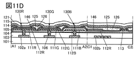
- 11A to 11D are cross-sectional views illustrating an example of a method for manufacturing a display device.
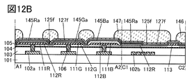
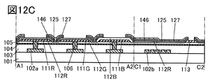
- 12A to 12C are cross-sectional views illustrating an example of a method for manufacturing a display device.
- 13A and 13B are cross-sectional views illustrating an example of a method for manufacturing a display device.
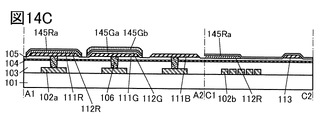
- 14A to 14D are cross-sectional views illustrating an example of a method for manufacturing a display device.
- 15A and 15B are cross-sectional views illustrating an example of a method for manufacturing a display device.
- 16A to 16G are plan views showing configuration examples of pixels.
- 17A to 17H are plan views showing configuration examples of pixels.
- FIG. 18 is a perspective view showing an example of a display device.
- FIG. 19A is a cross-sectional view showing an example of a display device.
- 19B and 19C are cross-sectional views showing examples of transistors.
- FIG. 20 is a cross-sectional view showing an example of a display device.
- 21A to 21D are cross-sectional views showing examples of display devices.
- 22A and 22B are perspective views showing an example of a display module.
- FIG. 23 is a cross-sectional view showing an example of a display device.
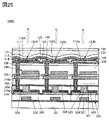
- FIG. 24 is a cross-sectional view showing an example of a display device.
- FIG. 25 is a cross-sectional view showing an example of a display device.
- FIG. 26 is a cross-sectional view showing an example of a display device.
- FIG. 27 is a cross-sectional view showing an example of a display device.
- FIG. 28 is a cross-sectional view showing an example of a display device.
- FIG. 29 is a cross-sectional view showing an example of a display device.
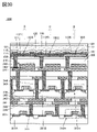
- FIG. 30 is a cross-sectional view showing an example of a display device.
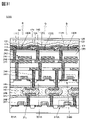
- FIG. 31 is a cross-sectional view showing an example of a display device.
- FIG. 32 is a cross-sectional view showing an example of a display device.
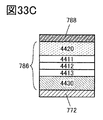
- 33A to 33F are diagrams showing configuration examples of light-emitting elements.
- 34A to 34D are diagrams showing examples of electronic devices.
- 35A to 35F are diagrams illustrating examples of electronic devices.
- 36A to 36G are diagrams showing examples of electronic devices.
- 37A to 37F are diagrams showing examples of electronic devices.
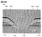
- 38A and 38B are STEM images of the cross section of the sample produced in this example.
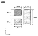
- FIG. 39 is a plan view showing the structure of the display panel manufactured in this example.
- FIG. 40 is an optical microscope photograph of the display panel produced in this example.
- FIG. 41 is a display photograph of the display panel manufactured in this example.
- FIG. 42 is a graph showing changes over time in luminance in the display panel manufactured in this example.
- FIG. 43 shows spectrum measurement results of the display panel manufactured in this example.
- film and “layer” can be interchanged depending on the case or circumstances.
- conductive layer or “insulating layer” may be interchangeable with the terms “conductive film” or “insulating film.”
- an EL layer refers to a layer provided between a pair of electrodes of a light-emitting element and containing at least a light-emitting substance (also referred to as a light-emitting layer) or a laminate including a light-emitting layer. .
- a display panel which is one mode of a display device, has a function of displaying (outputting) an image, for example, on a display surface. Therefore, the display panel is one aspect of the output device.
- the substrate of the display panel is attached with a connector such as FPC (Flexible Printed Circuit) or TCP (Tape Carrier Package), or an IC is attached to the substrate by COG (Chip On Glass) method.
- a connector such as FPC (Flexible Printed Circuit) or TCP (Tape Carrier Package)
- COG Chip On Glass
- One embodiment of the present invention is a display device including a pixel portion and a connection portion. Pixels are arranged in a matrix in the pixel portion.
- a pixel has at least two subpixels that emit light of different colors, and a light emitting element (also referred to as a light emitting device) is provided for each subpixel.
- Each light emitting element has a pixel electrode and a common electrode, and an EL layer is provided between the pixel electrode and the common electrode.
- a pixel electrode can be separated for each light emitting element, and a common electrode can be provided in common among the light emitting elements.
- the EL layer has at least a light-emitting layer, preferably a plurality of layers.
- the EL layer preferably has, for example, a light-emitting layer and a carrier-transporting layer (hole-transporting layer or electron-transporting layer) on the light-emitting layer.
- connection portion has a connection electrode, and a common electrode is provided so as to be electrically connected to the connection electrode.
- the connection electrodes are electrically connected to the FPC, for example. As described above, for example, by supplying the power supply potential to the FPC, the power supply potential can be supplied to the common electrode through the connection electrode.
- An electroluminescent element such as an organic EL element or an inorganic EL element can be used as the light emitting element provided in the pixel portion.
- LEDs light emitting diodes
- the light-emitting element of one embodiment of the present invention is preferably an organic EL element (organic electroluminescent element).
- Two or more light-emitting elements that emit different colors have EL layers each containing a different material.
- a full-color display device can be realized by including three types of light-emitting elements that emit red (R), green (G), and blue (B) light.
- an EL layer is processed into a fine pattern without using a shadow mask such as a metal mask.
- a shadow mask such as a metal mask.
- a device manufactured using a metal mask or FMM fine metal mask, high-definition metal mask
- a device with an MM (metal mask) structure is sometimes referred to as a device with an MML (metal maskless) structure.
- a first pixel electrode, a second pixel electrode, and a connection electrode are formed over an insulating layer.
- a first EL film is formed over the insulating layer, the first pixel electrode, and the second pixel electrode.
- the first EL film is also formed in the region between the pixel portion and the connection portion.
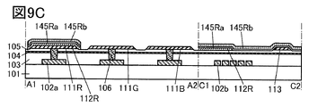
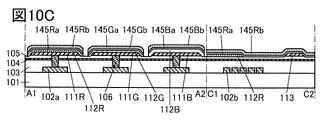
- a first sacrificial film is formed over the first EL film, the insulating layer, and the connection electrode. Specifically, a first sacrificial film is formed so as to cover the end of the first EL film and the end of the connection electrode. Subsequently, a resist mask is formed over the first sacrificial film. Subsequently, using a resist mask, the first sacrificial film and the first EL film are processed. Thus, a first EL layer having a region overlapping with the first pixel electrode and a first sacrificial layer over the first EL layer are formed. In addition, a second EL layer provided in a region between the pixel portion and the connection portion, and a second sacrificial layer covering an end portion of the second EL layer and an end portion of the connection electrode are formed.
- processing a film using a resist mask means removing a region of the film that does not overlap with the resist mask by etching.
- a method of processing using a photolithography method right above the film functioning as a light-emitting layer included in the first EL film can be considered.
- the light-emitting layer may be damaged (for example, by processing), and the reliability may be significantly impaired. Therefore, in order to manufacture a display device of one embodiment of the present invention, a film (eg, a carrier-transport layer or a carrier-injection layer, more specifically, an electron-transport layer, a A sacrificial layer or the like is formed on the film functioning as a transport layer, an electron injection layer, or a hole injection layer), and a film functioning as a light emitting layer is processed. Accordingly, the display device of one embodiment of the present invention can be a highly reliable display device. The same applies to the second EL film described later.
- a second EL film is formed over the insulating layer, the first sacrificial layer, the second pixel electrode, and the second EL layer.
- a second sacrificial film is formed on the second EL film and the second sacrificial layer.
- a resist mask is formed over the second sacrificial film.
- the second sacrificial film and the second EL film are processed.
- a third EL layer having a region overlapping with the second pixel electrode and a third sacrificial layer on the second EL layer are formed.
- the second sacrificial film and the second EL film are processed so that the second sacrificial film on the second sacrificial layer and the second EL film on the second EL layer are removed. do.
- the first to third EL layers have at least a light-emitting layer as described above.
- the first to third EL layers include one or more of a hole injection layer, a hole transport layer, a hole blocking layer, an electron blocking layer, an electron transport layer, and an electron injection layer.
- the first to third EL layers can have a structure in which a hole-injection layer, a hole-transport layer, a light-emitting layer, and an electron-transport layer are stacked in this order from the insulating layer side.
- the first to third EL layers can have a structure in which an electron-injection layer, an electron-transport layer, a light-emitting layer, and a hole-transport layer are stacked in this order from the insulating layer side.
- a common electrode is formed to form a first light emitting element and a second light emitting element. As mentioned above, the common electrode is electrically connected to the connection electrode.
- the second EL film is formed over the first EL layer. Therefore, when the first EL layer is thick, the side surfaces of the first EL layer may not be sufficiently covered with the second EL film. As a result, a recess may be formed in the second EL film in a region between the first EL layer and the second pixel electrode. In some cases, the second sacrificial film enters the concave portion, and a residue of the second sacrificial film remains in the concave portion after the second sacrificial film is processed. This may reduce the reliability of the display device. Therefore, the first EL layer is preferably thin.
- the thickness of the first EL layer is 200 nm or less, preferably 180 nm or less, more preferably 150 nm or less, and even more preferably 130 nm or less. Since the first EL layer is thin, the second EL film sufficiently covers the side surfaces of the first EL layer even when the second EL film is formed by a method with low coverage, It is possible to suppress the formation of the concave portion in the second EL film. Therefore, the display device of one embodiment of the present invention can be a highly reliable display device.
- the insulating layer can be formed by applying an insulating film containing a photosensitive material and processing the insulating film by a photolithography method.
- the difference in thickness between the first EL layer and the third EL layer is large, the thickness between the side surface of the first EL layer and the insulating layer or between the side surface of the third EL layer and the insulating layer is reduced. , cavities may form. The cavities make it easier for impurities to enter the EL layer, which may reduce the reliability of the display device.
- the difference in thickness between the first EL layer and the third EL layer is small.
- the difference in thickness between the first EL layer and the third EL layer is preferably 100 nm or less, more preferably 80 nm or less, more preferably 60 nm or less, and 40 nm. It is more preferably 30 nm or less, more preferably 30 nm or less.
- the display device of one embodiment of the present invention does not necessarily have the insulating layer containing the above organic material.
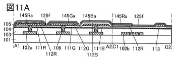
- the first EL layer can be provided to cover the edge of the first pixel electrode
- the third EL layer can be provided to cover the edge of the second pixel electrode.
- the first EL layer is also formed to have a tapered shape, and the coverage of the first pixel electrode with the first EL layer is improved. is possible and preferable.
- the third EL layer is also formed to have a tapered shape, so that the coverage of the second pixel electrode with the third EL layer is improved. is possible and preferable.
- foreign substances for example, dust, particles, or the like
- the manufacturing process can be preferably removed by cleaning or the like. It is preferable because it can be done.
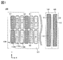
- FIG. 1 is a plan view showing a configuration example of a display device 100.
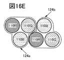
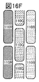
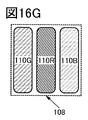
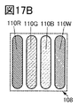
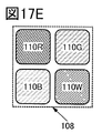
- the display device 100 has a pixel portion 107 in which a plurality of pixels 108 are arranged in a matrix.
- Pixel 108 has sub-pixel 110R, sub-pixel 110G, and sub-pixel 110B.
- FIG. 1 shows sub-pixels 110 of 2 rows and 6 columns, which form the pixels 108 of 2 rows and 2 columns.
- the sub-pixel 110 when describing matters common to the sub-pixel 110R, the sub-pixel 110G, and the sub-pixel 110B, the sub-pixel 110 may be referred to.
- Other constituent elements distinguished by alphabets may also be described using reference numerals with alphabets omitted when describing matters common to them.
- Subpixel 110R emits red light
- subpixel 110G emits green light
- subpixel 110B emits blue light. Accordingly, an image can be displayed on the pixel portion 107 . Therefore, the pixel portion 107 can be called a display portion.
- sub-pixels of three colors, red (R), green (G), and blue (B) will be described as an example.
- Sub-pixels of three colors (M) may be used.
- the number of types of sub-pixels is not limited to three, and may be four or more.
- the four sub-pixels are R, G, B, and white (W) sub-pixels, R, G, B, and Y sub-pixels, and R, G, B, infrared light ( IR), four sub-pixels, and so on.
- a stripe arrangement is applied to the pixels 108 shown in FIG.
- the arrangement method that can be applied to the pixels 108 is not limited to this, and an arrangement method such as a stripe arrangement, an S stripe arrangement, a delta arrangement, a Bayer arrangement, or a zigzag arrangement may be applied.
- a diamond array or the like can also be used.
- the row direction is sometimes called the X direction
- the column direction is sometimes called the Y direction.
- the X and Y directions intersect, for example perpendicularly intersect.
- FIG. 1 shows an example in which sub-pixels of different colors are arranged side by side in the X direction and sub-pixels of the same color are arranged side by side in the Y direction. Note that sub-pixels of different colors may be arranged side by side in the Y direction, and sub-pixels of the same color may be arranged side by side in the X direction.
- a region 141 and a connection portion 140 are provided outside the pixel portion 107 , and the region 141 is provided between the pixel portion 107 and the connection portion 140 .
- the EL layer 112 is provided in the region 141 .
- a connection electrode 113 is provided in the connection portion 140 .
- FIG. 1 shows an example in which the region 141 and the connection portion 140 are positioned on the right side of the pixel portion 107 in plan view, but the positions of the region 141 and the connection portion 140 are not particularly limited.
- the region 141 and the connection portion 140 may be provided in at least one of the upper side, the right side, the left side, and the lower side of the pixel portion 107 in plan view, and are provided so as to surround the four sides of the pixel portion 107 . good too.
- the upper surface shape of the region 141 and the connecting portion 140 can be band-shaped, L-shaped, U-shaped, frame-shaped, or the like. Also, the region 141 and the connecting portion 140 may be singular or plural.
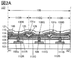
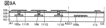
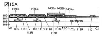
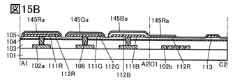
- FIG. 2A is a schematic cross-sectional view corresponding to the dashed-dotted line A1-A2 in FIG. 1
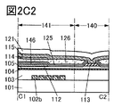
- FIG. 2B is a schematic cross-sectional view corresponding to the dashed-dotted line B1-B2 in FIG. It is the cross-sectional schematic corresponding to inside dashed-dotted line C1-C2.
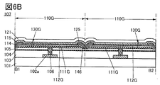
- the display device 100 includes an insulating layer 101, conductive layers 102a and 102b on the insulating layer 101, and conductive layers 102a and 102b on the insulating layer 101, conductive layers 102a, and 102b. , an insulating layer 104 on the insulating layer 103, and an insulating layer 105 on the insulating layer 104.
- An insulating layer 101 is provided on a substrate (not shown).
- the insulating layer 105, the insulating layer 104, and the insulating layer 103 are provided with openings reaching the conductive layer 102a, and plugs 106 are provided so as to fill the openings.
- a light-emitting element 130 is provided over the insulating layer 105 and the plug 106 in the pixel portion 107 .
- the insulating layer 101, the insulating layer 103, and the insulating layer 105 function as interlayer insulating layers.
- various inorganic insulating films such as an oxide insulating film, a nitride insulating film, an oxynitride insulating film, and a nitride oxide insulating film can be preferably used.
- a silicon oxide film, a silicon oxynitride film, an aluminum oxide film, a silicon nitride film, or a silicon nitride oxide film can be used.
- oxynitride refers to a material whose composition contains more oxygen than nitrogen
- nitride oxide refers to a material whose composition contains more nitrogen than oxygen. point to the material.
- silicon oxynitride refers to a material whose composition contains more oxygen than nitrogen
- silicon nitride oxide refers to a material whose composition contains more nitrogen than oxygen. indicates
- the insulating layer 104 functions as a barrier layer that prevents impurities such as water from entering the light emitting element 130, for example.
- a film into which hydrogen or oxygen is less likely to diffuse than a silicon oxide film such as a silicon nitride film, an aluminum oxide film, or a hafnium oxide film, can be used.
- the conductive layers 102a and 102b function as wirings.
- the conductive layer 102 a is provided in the pixel portion 107 and the conductive layer 102 b is provided in the region 141 .
- Conductive layer 102 a is electrically connected to light emitting element 130 through plug 106 .
- Various conductive materials can be used for the conductive layer 102a, the conductive layer 102b, and the plug 106, such as aluminum (Al), titanium (Ti), chromium (Cr), nickel (Ni), copper (Cu), yttrium. (Y), zirconium (Zr), tin (Sn), zinc (Zn), silver (Ag), platinum (Pt), gold (Au), molybdenum (Mo), tantalum (Ta), tungsten (W), etc. or an alloy containing this as a main component (such as an alloy of silver, palladium (Pd) and copper (Ag-Pd-Cu(APC))).
- oxide such as tin oxide or zinc oxide may be used for the conductive layers 102a, 102b, and the plugs 106 .
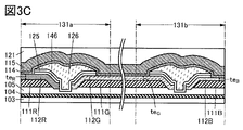
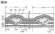
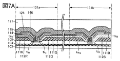
- FIG. 2A shows a cross-sectional configuration example of a light emitting element 130R provided in the sub-pixel 110R, a light emitting element 130G provided in the sub-pixel 110G, and a light emitting element 130B provided in the sub-pixel 110B.
- FIG. 2B shows a cross-sectional configuration example of the light emitting element 130G.
- an EL element such as an OLED (Organic Light Emitting Diode) or a QLED (Quantum-dot Light Emitting Diode).
- OLED Organic Light Emitting Diode
- QLED Quantum-dot Light Emitting Diode
- light-emitting substances that EL devices have include substances that emit fluorescence (fluorescent materials), substances that emit phosphorescence (phosphorescent materials), inorganic compounds (for example, quantum dot materials), and substances that exhibit heat-activated delayed fluorescence (heat-activated delayed fluorescent (thermally activated delayed fluorescence: TADF) material) and the like.
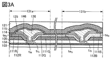
- the light emitting element 130R includes a pixel electrode 111R on the insulating layer 105 and the plug 106, an EL layer 112R on the pixel electrode 111R, a common layer 114 on the EL layer 112R, a common electrode 115 on the common layer 114, have
- the light emitting element 130G includes a pixel electrode 111G on the insulating layer 105 and on the plug 106, an EL layer 112G on the pixel electrode 111G, a common layer 114 on the EL layer 112G, a common electrode 115 on the common layer 114, have
- the light emitting element 130B includes the pixel electrode 111B on the insulating layer 105 and the plug 106, the EL layer 112B on the pixel electrode 111B, the common layer 114 on the EL layer 112B, the common electrode 115 on the common layer 114, have Note that the pixel electrode 111 may be called a lower electrode, and the common electrode 115 may be called an upper
- the pixel electrode 111 and the EL layer 112 are separately provided for each light emitting element 130 .
- the common layer 114 and the common electrode 115 are provided in common among the light emitting elements 130 .
- the EL layer 112R can be provided to cover the edge of the pixel electrode 111R, the EL layer 112G can be provided to cover the edge of the pixel electrode 111G, and the EL layer 112B can be provided to cover the edge of the pixel electrode 111B. It can be provided so as to cover the part.
- the EL layer 112R can be provided to cover the upper and lower ends of the pixel electrode 111R, and the EL layer 112G can be provided to cover the upper and lower ends of the pixel electrode 111G.
- 112B can be provided so as to cover the upper and lower ends of the pixel electrode 111B.
- the EL layer 112 is also formed to have a tapered shape, which is preferable because the coverage of the pixel electrode 111 with the EL layer 112 can be improved.
- the end portion of the pixel electrode 111 has a tapered shape, so that foreign substances (eg, dust, particles, or the like) in the manufacturing process can be preferably removed by a treatment such as cleaning.
- the EL layer 112 does not have to cover the end of the pixel electrode 111 , and for example, the end of the EL layer 112 may be located inside the end of the pixel electrode 111 .
- a tapered shape refers to a shape in which at least a part of the side surface of the structure is inclined with respect to the substrate surface.
- it refers to a shape having a region in which the angle formed by the inclined side surface and the substrate surface (also referred to as a taper angle) is less than 90°.
- insulating layer 105 may have recesses between adjacent light emitting elements 130 .
- the thickness of the insulating layer 105 in the region that does not overlap with the pixel electrode 111 may be thinner than the thickness of the insulating layer 105 in the region that overlaps with the pixel electrode 111 .
- the insulating layer 105 may not have recesses between the adjacent light emitting elements 130 in some cases.
- the EL layer 112R included in the light-emitting element 130R contains a light-emitting organic compound that emits light having an intensity in at least the red wavelength range.
- the EL layer 112G included in the light-emitting element 130G contains a light-emitting organic compound that emits light having an intensity in at least the green wavelength range.
- the EL layer 112B included in the light-emitting element 130B contains a light-emitting organic compound that emits light having an intensity in at least a blue wavelength range.
- a layer containing a light-emitting organic compound included in the EL layer 112 can be referred to as a light-emitting layer.
- the EL layer 112 has at least a light-emitting layer. Further, the EL layer 112 preferably has a light-emitting layer and a carrier-transport layer over the light-emitting layer. As a result, exposure of the light-emitting layer to the outermost surface can be suppressed during the manufacturing process of the display device 100, and damage to the light-emitting layer can be reduced. Thereby, the reliability of the display device 100 can be improved.
- the EL layer 112 can have one or more of a hole injection layer, a hole transport layer, a hole blocking layer, an electron blocking layer, an electron transport layer, and an electron injection layer.
- the EL layer 112 can have a structure in which a hole-injection layer, a hole-transport layer, a light-emitting layer, and an electron-transport layer are stacked in this order from the pixel electrode 111 side.
- the EL layer 112 can have a structure in which an electron-injection layer, an electron-transport layer, a light-emitting layer, and a hole-transport layer are stacked in this order from the pixel electrode 111 side.
- holes or electrons are sometimes referred to as “carriers”.
- the hole injection layer or electron injection layer is referred to as a "carrier injection layer”
- the hole transport layer or electron transport layer is referred to as a “carrier transport layer”
- the hole blocking layer or electron blocking layer is referred to as a "carrier It is sometimes called a block layer.
- the carrier injection layer, the carrier transport layer, and the carrier block layer described above may not be clearly distinguished from each other due to their cross-sectional shape, characteristics, or the like.
- one layer may serve two or three functions of the carrier injection layer, the carrier transport layer, and the carrier block layer.
- Common layer 114 can be an electron injection layer or a hole injection layer.
- EL layer 112 need not have an electron injection layer if common layer 114 has an electron injection layer, and EL layer 112 need not have a hole injection layer if common layer 114 has a hole injection layer.
- the common layer 114 it is preferable to use a material with as low electric resistance as possible.
- the thickness of the common layer 114 is preferably 1 nm or more and 5 nm or less, more preferably 1 nm or more and 3 nm or less.
- the common layer 114 may have a hole-transporting layer, a hole-blocking layer, an electron-blocking layer, or an electron-transporting layer. As described above, the common layer 114 can have at least one of a hole injection layer, a hole transport layer, a hole blocking layer, an electron blocking layer, an electron transport layer, or an electron injection layer. A layer included in the common layer 114 may have a structure not included in the EL layer 112 .
- a metal material for example, can be used as the pixel electrode 111 .
- the pixel electrode 111 may be a metal material such as gold, silver, platinum, magnesium, nickel, tungsten, chromium, molybdenum, iron, cobalt, copper, palladium, or titanium, or an alloy material containing the metal material (for example, silver and alloys of magnesium) can be used.
- a nitride of the metal material for example, titanium nitride
- the like may be used for the pixel electrode 111 .
- the common electrode 115 can be a conductive layer that transmits visible light.
- a conductive oxide such as indium oxide, indium tin oxide, indium zinc oxide, zinc oxide, or gallium-containing zinc oxide, or graphene can be used for the common electrode 115 .
- metal materials such as gold, silver, platinum, magnesium, nickel, tungsten, chromium, molybdenum, iron, cobalt, copper, palladium, and titanium, or alloy materials containing such metal materials can be used for the common electrode 115.
- a nitride of the metal material for example, titanium nitride
- the common electrode 115 a nitride of the metal material (for example, titanium nitride) or the like may be used for the common electrode 115 .
- a metal material or an alloy material (or a nitride thereof) is used, it is preferably thin enough to have translucency.
- a stacked film of any of the above materials can be used as the conductive layer.
- a protective layer 146 is provided over the EL layer 112 .
- a protective layer 146 is provided in a region of the EL layer 112 that is not in contact with the common layer 114 .
- the edge of the pixel electrode 111 may have a tapered shape. Thereby, the coverage of the protective layer 146 provided along the edge of the pixel electrode 111 can be improved. In addition, foreign substances (eg, dust, particles, or the like) generated during the manufacturing process of the display device 100 can be preferably removed by cleaning or the like.
- foreign substances eg, dust, particles, or the like
- An insulating layer 125 and an insulating layer 126 are provided in a region between two adjacent light emitting elements 130 .
- the insulating layer 125 is provided along the side surface of the EL layer 112, the side surface of the protective layer 146, the upper surface of the protective layer 146, and the upper surface of the insulating layer 105, for example.
- the insulating layer 126 is provided on the insulating layer 125 .
- the insulating layer 126 can fill recesses located between adjacent light emitting elements 130 . Thereby, the coverage of the common electrode 115 on the insulating layer 126 can be improved. Therefore, it is possible to suppress the occurrence of disconnection in the common electrode 115, thereby suppressing the occurrence of poor connection. In addition, it is possible to prevent the common electrode 115 from being locally thinned due to the steps and increasing the electrical resistance. As described above, the display device 100 can be a highly reliable display device.
- the insulating layer 125 is provided in contact with the side surface of the EL layer 112, a structure in which the EL layer 112 and the insulating layer 126 are not in contact can be employed.
- the EL layer 112 and the insulating layer 126 are in contact with each other, the EL layer 112 may be dissolved by an organic solvent contained in the insulating layer 126, especially when the EL layer 112 contains an organic compound. Therefore, as shown in FIGS. 2A and 2B, by providing the insulating layer 125 between the EL layer 112 and the insulating layer 126, the side surfaces of the EL layer 112 can be protected.
- the protective layer 146 and the insulating layer 125 can have inorganic materials.
- an inorganic insulating film such as an oxide insulating film, a nitride insulating film, an oxynitride insulating film, or a nitride oxide insulating film can be used, for example.
- the protective layer 146 and the insulating layer 125 may have a single-layer structure or a stacked-layer structure.
- the oxide insulating film includes a silicon oxide film, an aluminum oxide film, a magnesium oxide film, an indium gallium zinc oxide film, a gallium oxide film, a germanium oxide film, an yttrium oxide film, a zirconium oxide film, a lanthanum oxide film, a neodymium oxide film, and an oxide film.
- a hafnium film, a tantalum oxide film, and the like are included.
- the nitride insulating film include a silicon nitride film and an aluminum nitride film.
- Examples of the oxynitride insulating film include a silicon oxynitride film, an aluminum oxynitride film, and the like.
- nitride oxide insulating film examples include a silicon nitride oxide film, an aluminum nitride oxide film, and the like.
- an inorganic insulating film such as an aluminum oxide film, a hafnium oxide film, or a silicon oxide film formed by an atomic layer deposition (ALD) method to the protective layer 146 and the insulating layer 125, pinholes can be reduced.
- the protective layer 146 and the insulating layer 125 which have an excellent function of protecting the EL layer 112, can be formed.
- a sputtering method, a chemical vapor deposition (CVD) method, a pulsed laser deposition (PLD) method, an ALD method, or the like can be used to form the protective layer 146 and the insulating layer 125 .
- the insulating layer 125 is preferably formed by an ALD method with good coverage.
- Insulating layer 126 may comprise an organic material.
- acrylic resin, polyimide resin, epoxy resin, imide resin, polyamide resin, polyimideamide resin, silicone resin, siloxane resin, benzocyclobutene resin, phenolic resin, and precursors of these resins are applied. can do.
- the insulating layer 126 contains resin, the insulating layer 126 can be called a resin layer.
- an organic material such as polyvinyl alcohol (PVA), polyvinyl butyral, polyvinylpyrrolidone, polyethylene glycol, polyglycerin, pullulan, water-soluble cellulose, or alcohol-soluble polyamide resin may be used as the insulating layer 126 .
- PVA polyvinyl alcohol
- polyvinyl butyral polyvinylpyrrolidone
- polyethylene glycol polyglycerin
- pullulan polyethylene glycol
- polyglycerin polyglycerin
- pullulan polyethylene glycol
- pullulan polyglycerin
- pullulan water-soluble cellulose
- alcohol-soluble polyamide resin may be used as the insulating layer 126 .
- a photosensitive resin can be used for the insulating layer 126 .
- a photoresist may be used as the photosensitive resin.
- a positive material or a negative material can be used for the photosensitive resin.
- a colored material for example, a material containing a black pigment
- a material containing a black pigment may be used as the insulating layer 126 to block stray light from adjacent pixels and suppress color mixture.
- a reflective film for example, a metal film containing one or more selected from silver, palladium, copper, titanium, aluminum, and the like
- the display device 100 may be provided with a function of improving the light extraction efficiency by reflecting emitted light with the reflective film.
- a protective layer 121 is provided on the common electrode 115 to cover the light emitting element 130 .
- the protective layer 121 has a function of preventing impurities such as water from diffusing into the light emitting element 130 from above.
- the protective layer 121 can have, for example, a single-layer structure or a laminated structure including at least an inorganic insulating film.
- inorganic insulating films include oxide films or nitride films such as silicon oxide films, silicon oxynitride films, silicon nitride oxide films, silicon nitride films, aluminum oxide films, aluminum oxynitride films, and hafnium oxide films. be done.
- a semiconductor material such as indium gallium oxide or indium gallium zinc oxide may be used for the protective layer 121 .
- a laminated film of an inorganic insulating film and an organic insulating film can also be used as the protective layer 121 .
- a structure in which an organic insulating film is sandwiched between a pair of inorganic insulating films is preferable.
- the organic insulating film functions as a planarizing film.
- the upper surface of the organic insulating film can be flattened, so that the coverage of the inorganic insulating film thereon can be improved, and the barrier property can be enhanced.
- the upper surface of the protective layer 121 is flat, when a structure (for example, a color filter, an electrode of a touch sensor, or a lens array) is provided above the protective layer 121, unevenness due to the underlying structure may occur. This is preferable because it can reduce the impact.
- a structure for example, a color filter, an electrode of a touch sensor, or a lens array
- FIG. 2C1 is a cross-sectional view showing a configuration example of the region 141 and the connecting portion 140.
- FIG. 2C1 is a cross-sectional view showing a configuration example of the region 141 and the connecting portion 140.
- the conductive layer 102b is provided over the insulating layer 101
- the insulating layer 103 is provided over the insulating layer 101 and the conductive layer 102b.
- the EL layer 112 over the insulating layer 105, the protective layer 146 over the insulating layer 105 and the EL layer 112, the insulating layer 125 over the protective layer 146, and the insulating layer 126 over the insulating layer 125 , a common layer 114 on the insulating layer 126, a common electrode 115 on the common layer 114, and a protective layer 121 on the common electrode 115 are provided.
- the protective layer 146 is provided to cover the edge of the EL layer 112, for example.
- the EL layer 112 provided in the region 141 is not electrically connected to the common electrode 115 . Therefore, since the EL layer 112 provided in the region 141 can be applied with no voltage, the EL layer 112 provided in the region 141 can be configured not to emit light.
- the EL layer 112 provided in the region 141 is formed using at least a light-emitting organic compound that emits light having an intensity in the red wavelength region, a light-emitting organic compound that emits light having an intensity in the green wavelength region, or a blue wavelength region. Any luminescent organic compound that emits light with a high intensity. That is, the EL layer 112 provided in the region 141 can have the same structure as the EL layer 112R, the EL layer 112G, or the EL layer 112B of the light-emitting element 130.
- the insulating layers 105, 104, and 103 are partly etched or the like during the manufacturing process of the display device, although the details will be described later.
- the conductive layer 102b can be prevented from being exposed. Accordingly, the conductive layer 102b can be prevented from unintentionally contacting another electrode, layer, or the like. For example, a short circuit between the conductive layer 102b and the common electrode 115 can be prevented.
- the display device 100 can be a highly reliable display device. Further, since the display device 100 can be manufactured by a method with high yield, the display device 100 can be inexpensive.
- the connection section 140 has a connection electrode 113 on the insulating layer 105 , a common layer 114 on the connection electrode 113 , a common electrode 115 on the common layer 114 , and a protective layer 121 on the common electrode 115 .
- a protective layer 146 is provided so as to cover an end portion of the connection electrode 113, and an insulating layer 125, an insulating layer 126, a common layer 114, a common electrode 115, and a protective layer 121 are stacked in this order over the protective layer 146. provided.
- connection electrode 113 and the common electrode 115 are electrically connected at the connection portion 140 .
- the connection electrode 113 is electrically connected to, for example, an FPC (not shown). As described above, for example, by supplying the power supply potential to the FPC, the power supply potential can be supplied to the common electrode 115 via the connection electrode 113 .
- the electrical resistance of the common layer 114 in the thickness direction is negligibly small, even if the common layer 114 is provided between the connection electrode 113 and the common electrode 115, Conduction with the common electrode 115 can be ensured.
- a mask for defining a film forming area to be distinguished from a fine metal mask, it is also called an area mask or a rough metal mask).
- the manufacturing process of the display device 100 can be simplified.
- FIG. 2C2 is a modification of the configuration shown in FIG. 2C1.
- FIG. 2C2 shows a configuration example in which the connection portion 140 is not provided with the common layer 114 .
- the connection electrode 113 and the common electrode 115 can be in contact with each other. Thereby, the electrical resistance between the connection electrode 113 and the common electrode 115 can be reduced.
- FIG. 2C2 shows a structure in which the common layer 114 is provided in a region overlapping with the EL layer 112 in the region 141 and the common layer 114 is not provided in a region not overlapping with the EL layer 112; Not limited.
- the common layer 114 may not be provided in a region that overlaps with the EL layer 112 , or the common layer 114 may be provided in a region that does not overlap with the EL layer 112 .
- FIG. 3A is an enlarged view of a region 131a between the light emitting elements 130R and 130G and a region 131b between the light emitting elements 130G and 130B in FIG. 2A.
- FIG. 3A shows a configuration example in which the thickness teB of the EL layer 112B is thicker than the thickness teR of the EL layer 112R, and the thickness teR of the EL layer 112R is thicker than the thickness teG of the EL layer 112G.
- the film thickness te R , the film thickness te G , and the film thickness te B are reduced, the occurrence of defects due to the manufacturing process of the display device 100 can be suppressed. Accordingly, the display device 100 can be a highly reliable display device. In addition, the yield in manufacturing the display device 100 can be increased, and the display device 100 can be inexpensive.
- the film thickness te R , the film thickness te G , and the film thickness te B should be 200 nm or less. is preferable, and 180 nm or less is more preferable.
- Two of the film thickness te R , the film thickness te G , and the film thickness te B are preferably 150 nm or less, more preferably 130 nm or less.
- the distance between the upper surface of the pixel electrode 111R and the lower surface of the common layer 114 is defined as film thickness teR
- the distance between the upper surface of the pixel electrode 111G and the lower surface of the common layer 114 is defined as film thickness teG
- the pixel The distance between the top surface of the electrode 111B and the bottom surface of the common layer 114 can also be the film thickness teB .
- the distance between the upper surface of the pixel electrode 111R and the lower surface of the common electrode 115 is defined as film thickness teR
- the distance between the upper surface of the pixel electrode 111G and the lower surface of the common electrode 115 is defined as film thickness teG
- the pixel electrode The distance between the upper surface of 111B and the lower surface of the common electrode 115 can also be the film thickness teB .
- the distance between the upper surface of the pixel electrode 111R and the lower surface of the common electrode 115 is defined by the thickness te R
- the distance between the top surface of the pixel electrode 111G and the bottom surface of the common electrode 115 is defined as teG
- the distance between the top surface of the pixel electrode 111B and the bottom surface of the common electrode 115 is defined as teB .
- a cavity may be formed between the side surface of the EL layer 112 and the insulating layer 126 in the region 131a.
- a cavity is formed between the insulating layer 126 and the side surface of the EL layer 112 having the smaller thickness among the EL layers 112R and 112G.
- a cavity may be formed between the side surface of the EL layer 112 and the insulating layer 126 in the region 131b.
- a cavity may be formed between the insulating layer 126 and the side surface of the EL layer 112 having the smaller thickness between the EL layer 112G and the EL layer 112B.
- the formation of such cavities makes it easier for impurities to enter the EL layer 112, which may reduce the reliability of the display device.
- the difference between the film thickness te R , the film thickness te G , and the film thickness te B is small.
- the difference between the largest film thickness and the smallest film thickness is preferably 100 nm or less, more preferably 90 nm or less. It is preferably 85 nm or less, more preferably 80 nm or less. Accordingly, the above cavity is not formed, and the display device 100 can be a highly reliable display device.
- the term “difference” between the first value and the second value indicates the absolute value of the value obtained by subtracting the second value from the first value.
- the difference between the first film thickness and the second film thickness indicates the absolute value of the value obtained by subtracting the second film thickness from the first film thickness.
- the value including the sign may be called "difference”.
- the difference between the first value and the second value may be a negative value.
- the insulating layer 105 has a film thickness ti R in a region in contact with the lower surface of the EL layer 112R, a film thickness ti G in a region in contact with the lower surface of the EL layer 112G, and a film thickness ti G in a region in contact with the lower surface of the EL layer 112B.
- ti B are equal to each other, but the present invention is not limited to this.
- FIG. 3B shows an example in which the film thickness tiG is smaller than the film thickness tiR and the film thickness tiB is smaller than the film thickness tiG .
- the film thickness ti R , the film thickness ti G , and the film thickness ti B may differ from each other due to the manufacturing process of the display device 100 to be described later. Further, as shown in FIG. 3B, the thickness of the insulating layer 105 in the region in contact with the lower surface of the insulating layer 125 may be smaller than any of the thickness ti R , the thickness ti G , and the thickness ti B. be.
- FIG. 3C is a modification of the configuration shown in FIG. 3A, showing an example in which film thickness teB is smaller than film thickness teR and film thickness teG .
- the film thickness teB is smaller than the film thickness teG
- the film thickness teG is smaller than the film thickness teR .
- FIG. 4A is a modification of the configuration shown in FIG. 3A, and shows an example in which the end of the protective layer 146, the end of the insulating layer 125, and the end of the insulating layer 126 are aligned with the upper end 133 of the pixel electrode 111.
- FIG. showing. FIG. 4B is a modification of the configuration shown in FIG. 4A, in which the end of the protective layer 146, the end of the insulating layer 125, and the end of the insulating layer 126 are located inside the upper end 133 of the pixel electrode 111 (the light emitting region). side). That is, FIG.
- FIG. 4B shows an example in which a part of the upper surface of the pixel electrode 111 overlaps with the protective layer 146, the insulating layer 125, and the insulating layer 126.
- FIG. 4C is a modification of the configuration shown in FIG. 4A, in which the edge of the protective layer 146, the edge of the insulating layer 125, and the edge of the insulating layer 126 overlap the side surface (tapered portion) of the pixel electrode 111.
- An example corresponding to the top edge 134 of the EL layer 112 is shown.
- the upper end portion 134 is located outside the upper end portion 133 (on the side opposite to the light emitting region), the end portions of the protective layer 146, the insulating layer 125, and the insulating layer 126 are located on the edge of the pixel electrode 111. It is positioned outside the upper end portion 133 (on the side opposite to the light emitting region).
- the area of the region where the pixel electrode 111, the EL layer 112, and the common electrode 115 overlap without interposing the insulating layer 126 is larger than that in the structure shown in FIG. 4B. can do.
- the display device 100 having the structure shown in FIG. 4A and the display device 100 having the structure shown in FIG. 4C can have a wider light-emitting area than the display device 100 having the structure shown in FIG. 4B, so that the aperture ratio can be increased.
- the display device 100 having the structure shown in FIG. 4B can be manufactured more easily than the display device 100 having the structure shown in FIG. 4A and the display device 100 having the structure shown in FIG. 4C.
- FIG. 4C shows an example in which the length xt in the X direction of the region of the EL layer 112 in contact with the upper surface of the insulating layer 105 is shorter than the structures shown in FIGS. 4A and 4B. Accordingly, in the configuration shown in FIG. 4C, the area of the pixel electrode 111 can be made larger than in the configuration shown in FIG. 4A and the configuration shown in FIG. 4B. Therefore, in the structure shown in FIG. 4C, the area of the region where the pixel electrode 111, the EL layer 112, and the common electrode 115 overlap each other without the insulating layer 126 interposed between the structure shown in FIG. 4A and the structure shown in FIG. 4B. can be made larger. As described above, the display device 100 having the configuration shown in FIG. 4C can have a higher aperture ratio than the display device 100 having the configuration shown in FIG. 4A and the display device 100 having the configuration shown in FIG. 4B.
- FIG. 5A shows an example in which a protective layer 151 is provided between the insulating layer 126 and the common layer 114 and the edge of the protective layer 151 matches the edge of the insulating layer 126 in the configuration shown in FIG.
- FIG. 5B shows an example in which a protective layer 151 is provided between the insulating layer 126 and the common layer 114 and the protective layer 151 covers the edge of the insulating layer 126 in the configuration shown in FIG. 4C. That is, in the configuration shown in FIG. 5B , the edge of the protective layer 151 overlaps the upper surface of the pixel electrode 111 .
- the protective layer 151 is preferably a layer with high barrier properties against oxygen, water, and the like. This can prevent impurities such as oxygen and water contained in the insulating layer 126 , which may include an organic insulating material such as resin, from entering the common layer 114 . Therefore, the display device 100 can be a highly reliable display device.
- an inorganic insulating material can be used, such as nitride.
- the protective layer 151 may include at least one of silicon nitride, aluminum nitride, or hafnium nitride.
- an oxide or an oxynitride can be used as the protective layer 151.
- an oxide film or an oxynitride such as silicon oxide, silicon oxynitride, aluminum oxide, aluminum oxynitride, hafnium oxide, or hafnium oxynitride can be used.
- a film can be used.
- the protective layer 151 can be formed using, for example, a sputtering method, a CVD method, a vacuum deposition method, a PLD method, or an ALD method.
- the display device 100 having the configuration shown in FIG. 5A can have a higher aperture ratio than the display device 100 having the configuration shown in FIG. 5B.
- the display device 100 having the structure shown in FIG. 5B can be manufactured more easily than the display device 100 having the structure shown in FIG. 5A.
- FIGS. 6A, 6B, 6C1, 6C2, 7A, 7B, and 7C show the configurations shown in FIGS. 2A, 2B, 2C1, 2C2, 3A, 3B, and 3C, respectively.
- a modification is shown, and an example in which the insulating layer 126 is not provided is shown. If the insulating layer 126 is not provided, the common layer 114 has regions located between adjacent EL layers 112, for example as shown in FIG. 7A. Additionally, the common electrode 115 may also have regions located between adjacent EL layers 112 .
- FIG. 8A is a modification of the configuration shown in FIG. 7A, showing an example in which a protective layer 127 is provided between the insulating layer 125 and the common layer 114.
- FIG. 8B is a cross-sectional view showing a configuration example of the connection portion 140 and the region 141 in the display device 100 having the configuration shown in FIG. 8A. As shown in FIG. 8A, the edges of the protective layer 127 can coincide with the edges of the insulating layer 125 .
- the display device 100 can be a highly reliable display device.
- a material that can be used for the insulating layer 125 can be used for the protective layer 127 .
- a nitride insulating film such as a silicon nitride film or an aluminum nitride film can be preferably used as the protective layer 127 .
- the protective layer 127 can be formed by a sputtering method, a CVD method, a PLD method, an ALD method, or the like. It is preferably formed using a method.
- a metal oxide such as indium gallium zinc oxide (In—Ga—Zn oxide) can be used as the protective layer 127 .
- indium oxide, indium zinc oxide (In—Zn oxide), indium tin oxide (In—Sn oxide), indium titanium oxide (In—Ti oxide), indium tin zinc oxide (In—Sn -Zn oxide), indium titanium zinc oxide (In-Ti-Zn oxide), indium gallium tin zinc oxide (In-Ga-Sn-Zn oxide), or the like can be used.
- indium tin oxide containing silicon or the like can be used.
- element M is aluminum, silicon, boron, yttrium, copper, vanadium, beryllium, titanium, iron, nickel, germanium, zirconium, molybdenum, lanthanum, cerium, neodymium, hafnium, tantalum, tungsten , or one or more selected from magnesium).
- M is preferably one or more selected from gallium, aluminum, and yttrium.
- the protective layer 127 can be formed using a sputtering method.
- thin films (an insulating film, a semiconductor film, a conductive film, or the like) forming a display device can be formed by a sputtering method, a CVD method, a vacuum evaporation method, a PLD method, an ALD method, or the like.
- the CVD method includes a plasma enhanced CVD (PECVD) method, a thermal CVD method, and the like.
- one of the thermal CVD methods is the metal organic CVD (MOCVD) method.
- the ALD method includes the PEALD method, the thermal ALD method, and the like.
- thin films that make up the display device can be formed by spin coating, dipping, spray coating, inkjet, dispensing, screen printing, offset printing, doctor knife method, slit coating, roll coating, It can be formed by a method such as curtain coating or knife coating.
- the thin film when processing the thin film that constitutes the display device, for example, a photolithography method can be used.
- the thin film may be processed by a nanoimprint method, a sandblast method, a lift-off method, or the like.
- an island-shaped thin film may be directly formed by a film formation method using a shielding mask such as a metal mask.
- the photolithography method there are typically the following two methods.
- One is a method of forming a resist mask on a thin film to be processed, processing the thin film by etching, for example, and removing the resist mask.
- the other is a method of forming a thin film having photosensitivity and then exposing and developing the thin film to process the thin film into a desired shape.
- the light used for exposure may be, for example, i-line (wavelength 365 nm), g-line (wavelength 436 nm), h-line (wavelength 405 nm), or a mixture thereof.
- ultraviolet rays, KrF laser light, ArF laser light, or the like can also be used.
- extreme ultraviolet (EUV: Extreme Ultra-Violet) light or X-rays may be used.
- An electron beam can also be used instead of the light used for exposure.
- the use of extreme ultraviolet light, X-rays, or electron beams is preferable because extremely fine processing is possible.
- a photomask is not necessary when exposure is performed by scanning a beam such as an electron beam.
- a dry etching method, a wet etching method, a sandblasting method, or the like can be used for etching the thin film.
- 9A to 11D are cross-sectional views showing an example of a method for manufacturing the display device 100 in which the light emitting element 130 has the configuration shown in FIG. 2A and the connection portion 140 has the configuration shown in FIG. 2C1.
- 9A to 11D show a cross-sectional view corresponding to the dashed-dotted line A1-A2 in FIG. 1 and a cross-sectional view corresponding to the dashed-dotted line C1-C2.
- an insulating layer 101 is formed on a substrate (not shown). Subsequently, a conductive layer 102a and a conductive layer 102b are formed over the insulating layer 101, and an insulating layer 103 is formed over the insulating layer 101 so as to cover the conductive layer 102a and the conductive layer 102b. Subsequently, an insulating layer 104 is formed over the insulating layer 103 and an insulating layer 105 is formed over the insulating layer 104 .
- a substrate having heat resistance that can withstand at least subsequent heat treatment can be used.
- a glass substrate, a quartz substrate, a sapphire substrate, a ceramic substrate, an organic resin substrate, or the like can be used.
- a semiconductor substrate such as a single crystal semiconductor substrate, a polycrystalline semiconductor substrate, a compound semiconductor substrate made of silicon germanium or the like, or an SOI substrate made of silicon, silicon carbide, or the like can be used.
- openings are formed in the insulating layers 105, 104, and 103 to reach the conductive layer 102a. Subsequently, a plug 106 is formed so as to fill the opening.
- a conductive film that will later become the pixel electrode 111 and the connection electrode 113 is formed over the insulating layer 105 and the plug 106 .
- part of the conductive film is processed by etching or the like to form a pixel electrode 111R, a pixel electrode 111G, and a pixel electrode 111B on the insulating layer 105 and the plug .
- a connection electrode 113 is formed on the insulating layer 105 (FIG. 9A).
- the conductive film is preferably processed so that the side surface of the pixel electrode 111 and the side surface of the connection electrode 113 are tapered.
- foreign matter generated in the subsequent steps can be preferably removed by a treatment such as cleaning.
- the thickness of the insulating layer 105 in a region that does not overlap with the pixel electrode 111 or the connection electrode 113 may be smaller than the thickness of the insulating layer 105 in a region that overlaps with the pixel electrode 111 or the connection electrode 113 .
- the recess may not be formed in the insulating layer 105 in some cases.
- an EL film 112Rf that will later become the EL layer 112R is formed on the insulating layer 105, the pixel electrode 111, and the connection electrode 113. Then, as shown in FIG. Here, the EL film 112 Rf can be provided so as not to overlap with the connection electrode 113 .
- the EL film 112Rf can be formed so as not to overlap with the connection electrode 113 by shielding the region including the connection electrode 113 with a metal mask and forming the EL film 112Rf. Since the metal mask used at this time does not need to shield the pixel region of the display section, it is not necessary to use a high-definition mask, and for example, a rough metal mask can be used.
- the EL film 112Rf has at least a film (light-emitting film) containing a light-emitting compound. Further, the EL film 112Rf preferably has a light emitting film and a film functioning as a carrier transport layer on the light emitting film. As a result, it is possible to prevent the light-emitting film from being exposed to the outermost surface during the manufacturing process of the display device 100, and reduce damage to the light-emitting film. Thereby, the reliability of the display device 100 can be improved.
- the EL film 112Rf has a structure in which one or more of films functioning as a hole injection layer, a hole transport layer, a hole block layer, an electron block layer, an electron transport layer, or an electron injection layer are laminated. be able to.
- the EL film 112Rf can have a structure in which a film functioning as a hole injection layer, a film functioning as a hole transporting layer, a light emitting film, and a film functioning as an electron transporting layer are laminated in this order.
- the EL film 112Rf can have a structure in which a film functioning as an electron injection layer, a film functioning as an electron transporting layer, a light emitting film, and a film functioning as a hole transporting layer are laminated in this order.
- the EL film 112Rf can be formed, for example, by a vapor deposition method, a sputtering method, an inkjet method, or the like. Note that the method is not limited to this, and the film forming method described above can be used as appropriate.
- a sacrificial film 144Ra is formed on the insulating layer 105, the EL film 112Rf, and the connection electrode 113, and a sacrificial film 144Rb is formed on the sacrificial film 144Ra. That is, a sacrificial film having a two-layer structure is formed over the insulating layer 105, the EL film 112Rf, and the connection electrode 113.
- the sacrificial film may have a single layer structure, or may have a laminated structure of three or more layers.
- the sacrificial film When the sacrificial film is formed in the subsequent steps, the sacrificial film has a two-layer laminated structure, but may have a single layer structure or a laminated structure of three or more layers.
- the sacrificial film 144Ra can be formed so as to cover the end of the EL film 112Rf.
- a sputtering method for example, a CVD method, an ALD method, or a vacuum deposition method can be used.
- a formation method that causes little damage to the EL film is preferable, and the sacrificial film 144Ra directly formed on the EL film 112Rf is preferably formed using an ALD method or a vacuum evaporation method.
- an inorganic film such as a metal film, an alloy film, a metal oxide film, a semiconductor film, or an inorganic insulating film, or an organic film such as an organic insulating film can be preferably used.
- an oxide film can be used as the sacrificial film 144Ra.
- an oxide film or an oxynitride film such as silicon oxide, silicon oxynitride, aluminum oxide, aluminum oxynitride, hafnium oxide, or hafnium oxynitride can be used.
- a nitride film for example, can also be used as the sacrificial film 144Ra.
- nitrides such as silicon nitride, aluminum nitride, hafnium nitride, titanium nitride, tantalum nitride, tungsten nitride, gallium nitride, and germanium nitride can also be used.
- a film containing such an inorganic insulating material can be formed using a film formation method such as a sputtering method, a CVD method, or an ALD method. It is preferably formed using a method.
- metal materials such as nickel, tungsten, chromium, molybdenum, cobalt, palladium, titanium, aluminum, yttrium, zirconium, and tantalum, or alloy materials containing such metal materials can be used.
- a low melting point material such as aluminum or silver.
- a metal oxide such as indium gallium zinc oxide (In--Ga--Zn oxide) can be used as the sacrificial film 144Ra.
- indium oxide, indium zinc oxide (In—Zn oxide), indium tin oxide (In—Sn oxide), indium titanium oxide (In—Ti oxide), indium tin zinc oxide (In—Sn -Zn oxide), indium titanium zinc oxide (In-Ti-Zn oxide), indium gallium tin zinc oxide (In-Ga-Sn-Zn oxide), or the like can be used.
- indium tin oxide containing silicon or the like can be used.
- element M is aluminum, silicon, boron, yttrium, copper, vanadium, beryllium, titanium, iron, nickel, germanium, zirconium, molybdenum, lanthanum, cerium, neodymium, hafnium, tantalum, tungsten , or one or more selected from magnesium).
- M is preferably one or more selected from gallium, aluminum, and yttrium.
- a material that can be used as the sacrificial film 144Ra can be used.
- one material can be selected for the sacrificial film 144Ra and the other can be selected for the sacrificial film 144Rb from the materials that can be used for the sacrificial film 144Ra listed above.
- one or a plurality of materials are selected for the sacrificial film 144Ra from among the materials that can be used for the sacrificial film 144Ra, and materials other than those selected for the sacrificial film 144Ra are selected for the sacrificial film 144Rb.
- One or more materials can be used.
- the film formation temperature for film formation by the ALD method and the sputtering method is room temperature or higher and 120° C. or lower, preferably room temperature or higher and 100° C. or lower, so that the influence on the EL film 112Rf is minimized. It is preferable because it can be reduced.
- the stress of the laminated structure is small.
- the stress of the laminated structure is ⁇ 500 MPa or more and +500 MPa or less, more preferably ⁇ 200 MPa or more and +200 MPa or less, process troubles such as film peeling and peeling can be suppressed, which is preferable.
- a film having high resistance to the etching process of each EL film such as the EL film 112Rf, that is, a film having a high etching selectivity can be used.
- a material that can be dissolved in a chemically stable solvent may be used as the sacrificial film 144Ra.
- a material that dissolves in water or alcohol can be suitably used for the sacrificial film 144Ra.
- the sacrificial film 144Ra is dissolved in a solvent such as water or alcohol and applied by a wet film forming method, and then heat-treated to evaporate the solvent.
- the solvent can be removed at a low temperature in a short time by performing heat treatment in a reduced pressure atmosphere, so that thermal damage to the EL film 112Rf can be reduced, which is preferable.
- wet film formation methods that can be used to form the sacrificial film 144Ra include spin coating, dipping, spray coating, inkjet, dispensing, screen printing, offset printing, doctor knife method, slit coating, roll coating, curtain coating, and the like. There are knife courts, etc.
- an organic material such as polyvinyl alcohol (PVA), polyvinyl butyral, polyvinylpyrrolidone, polyethylene glycol, polyglycerin, pullulan, water-soluble cellulose, or alcohol-soluble polyamide resin can be used.
- PVA polyvinyl alcohol
- polyvinyl butyral polyvinylpyrrolidone
- polyethylene glycol polyglycerin
- pullulan polyethylene glycol
- pullulan polyglycerin
- pullulan water-soluble cellulose
- alcohol-soluble polyamide resin water-soluble polyamide resin
- a film having a high etching selectivity with respect to the sacrificial film 144Ra may be used for the sacrificial film 144Rb.
- an inorganic insulating material such as aluminum oxide, hafnium oxide, or silicon oxide formed by ALD is used, and as the sacrificial film 144Rb, nickel, tungsten, chromium, molybdenum, cobalt, palladium, Metal materials such as titanium, aluminum, yttrium, zirconium, and tantalum, or alloy materials containing these metal materials are preferably used. In particular, it is preferable to use tungsten formed by a sputtering method as the sacrificial film 144Rb.
- a metal oxide containing indium such as indium gallium zinc oxide (In--Ga--Zn oxide) formed by a sputtering method may be used.
- an inorganic material may be used as the sacrificial film 144Rb.
- an oxide film or a nitride film such as a silicon oxide film, a silicon oxynitride film, a silicon nitride oxide film, a silicon nitride film, an aluminum oxide film, an aluminum oxynitride film, or a hafnium oxide film can be used.
- an organic film that can be used for the EL film 112Rf may be used as the sacrificial film 144Rb.
- the same organic film as the EL film 112Rf can be used as the sacrificial film 144Rb.
- the use of such an organic film is preferable because the EL film 112Rf and the deposition apparatus can be used in common.
- the sacrificial film 144Rb can be removed at the same time when the EL film 112Rf is etched, the process can be simplified.
- a resist mask 143a is formed on the sacrificial film 144Rb (FIG. 9B).
- a resist material containing a photosensitive resin such as a positive resist material or a negative resist material can be used.
- portions of the sacrificial films 144Rb and 144Ra that are not covered with the resist mask 143a are removed by etching to form island-like or strip-like sacrificial layers 145Rb and 145Ra.
- the sacrificial layer 145Rb and the sacrificial layer 145Ra can be formed, for example, on the pixel electrode 111R and in the region indicated by the dashed-dotted line C1-C2 (the region corresponding to the region 141 and the connecting portion 140 shown in FIG. 1).
- part of the insulating layer 105 may be etched.
- the sacrificial film 144Rb and the sacrificial film 144Ra in the region corresponding to the region 141 shown in FIG. may be exposed.
- a film formed in a later step may unintentionally come into contact with the conductive layer 102b, causing a short circuit.
- the conductive layer 102b may be short-circuited with the common electrode 115 formed in a later step.
- a sacrificial layer 145Ra and a sacrificial layer 145Rb are also formed in a region corresponding to the region 141 illustrated in FIG. Specifically, a sacrificial layer 145Ra and a sacrificial layer 145Rb are formed so as to cover the end of the EL layer 112R provided in the region corresponding to the region 141 and the end of the connection electrode 113 . Accordingly, exposure of the conductive layer 102b can be prevented, and the display device 100 can be a highly reliable display device. In addition, since the display device 100 can be manufactured by a high-yield method, the display device 100 can be inexpensive.
- a part of the sacrificial film 144Rb is removed by etching using the resist mask 143a, and after the sacrificial layer 145Rb is formed, the resist mask 143a is removed, and then the sacrificial film 144Ra is etched using the sacrificial layer 145Rb as a hard mask. is preferred.
- a wet etching method or a dry etching method can be used for etching for forming the hard mask, and the use of the dry etching method can suppress pattern shrinkage.
- Processing of the sacrificial films 144Ra and 144Rb and removal of the resist mask 143a can be performed by a wet etching method or a dry etching method.
- the sacrificial film 144Ra and the sacrificial film 144Rb can be processed by a dry etching method using gas containing fluorine.
- the resist mask 143a can be removed by a dry etching method (also referred to as a plasma ashing method) using a gas containing oxygen (also referred to as an oxygen gas).
- the resist mask 143a can be removed while the EL film 112Rf is covered with the sacrificial film 144Ra.
- the EL film 112Rf is exposed to oxygen, it may adversely affect the electrical characteristics of the light emitting element 130R. Therefore, when removing the resist mask 143a by a method using oxygen gas such as plasma ashing, it is preferable to etch the sacrificial film 144Ra using the sacrificial layer 145Rb as a hard mask.
- a portion of the EL film 112Rf that is not covered with the sacrificial layer 145Ra is removed by etching to form an island-shaped or strip-shaped EL layer 112R (FIG. 9C).
- the EL layer 112R is also formed in a region corresponding to the region 141 shown in FIG.
- the etching of the EL film 112Rf may etch the insulating layer 105 in a region that overlaps neither the sacrificial layer 145R nor the pixel electrode 111 .
- the thickness of the insulating layer 105 in the region where the upper surface is exposed may be smaller than the thickness of the insulating layer 105 in other regions. Therefore, as shown in FIG. 3B, the film thickness ti G and the film thickness ti B may be smaller than the film thickness ti R . Note that when the etching selectivity between the EL film 112Rf and the insulating layer 105 is high, the insulating layer 105 may not be etched.
- the sacrificial layer 145R when describing items common to the sacrificial layer 145Ra and the sacrificial layer 145Rb, the sacrificial layer 145R may be referred to.
- the sacrificial layer 145a when describing items common to the sacrificial layer 145Ra, the sacrificial layer 145Ga, and the sacrificial layer 145Ba, the sacrificial layer 145a may be referred to.
- the sacrificial layer 145b when describing items common to the sacrificial layer 145Rb, the sacrificial layer 145Gb, and the sacrificial layer 145Bb, they may be referred to as the sacrificial layer 145b.
- the sacrificial layer 145 when describing items common to the sacrificial layer 145a and the sacrificial layer 145b, they may be referred to as the sacrificial layer 145 in some cases. Other components may also be described using reference numerals with abbreviated alphabets as described above.
- the etching rate can be increased by using a dry etching method using oxygen gas for etching the EL film 112Rf. Therefore, etching can be performed under low-power conditions while maintaining a sufficiently high etching rate, so that damage due to etching can be reduced. Furthermore, problems such as adhesion of reaction products to the EL layer 112R generated during etching can be suppressed.
- Etching gases containing no oxygen as a main component include, for example, gases containing CF 4 , C 4 F 8 , SF 6 , CHF 3 , Cl 2 , H 2 O, BCl 3 and the like, and group 18 elements such as He. gas containing. Further, a mixed gas of the above gas and a diluent gas that does not contain oxygen can be used as an etching gas. Etching of the EL film 112Rf is not limited to the above, and may be performed by a dry etching method using another gas or by a wet etching method.
- the EL layer 112R is formed by etching the EL film 112Rf, if impurities adhere to the side surface of the EL layer 112R, the impurities may penetrate into the EL layer 112R in subsequent steps. This may reduce the reliability of the display device 100 . Therefore, it is preferable to remove impurities attached to the surface of the EL layer 112R after the EL layer 112R is formed, because the reliability of the display device 100 can be improved.
- Impurities adhering to the surface of the EL layer 112R can be removed, for example, by irradiating the surface of the EL layer 112R with an inert gas.
- the surface of the EL layer 112R is exposed immediately after the EL layer 112R is formed. Specifically, the side surface of the EL layer 112R is exposed. Therefore, if the substrate on which the EL layer 112R is formed is placed in an inert gas atmosphere after the EL layer 112R is formed, the impurities adhering to the EL layer 112R can be removed.
- the inert gas for example, any one or more selected from group 18 elements (typically helium, neon, argon, xenon, krypton, etc.) and nitrogen can be used.
- a method of processing using a photolithography method right above the light-emitting film of the EL film 112Rf can be considered.
- the light-emitting layer may be damaged (for example, by processing), and the reliability may be significantly impaired. Therefore, in order to manufacture the display device 100, a film (for example, a carrier transport layer or a carrier injection layer, more specifically an electron transport layer, a hole transport layer, an electron injection layer, or a positive electrode layer) positioned above the light emitting film is used.
- a sacrificial layer 145Ra and a sacrificial layer 145Rb are formed on the film functioning as a hole injection layer), and the light emitting film is processed. Accordingly, the display device 100 can be a highly reliable display device.
- an EL film 112Gf which will later become the EL layer 112G, is formed on the insulating layer 105, the sacrificial layer 145Rb, the pixel electrode 111G, and the pixel electrode 111B.
- the EL film 112Gf After forming the sacrificial layer 145Ra, it is possible to prevent the EL film 112Gf from contacting the upper surface of the EL layer 112R.
- the description of the formation of the EL film 112Rf can be referred to.
- a sacrificial film 144Ga is formed on the EL film 112Gf and the sacrificial layer 145Rb, and a sacrificial film 144Gb is formed on the sacrificial film 144Ga.
- a resist mask 143b is formed on the sacrificial film 144Gb (FIG. 9D1).
- the sacrificial film 144Ga can be formed so as to cover the end of the EL film 112Gf.
- the description of the formation of the sacrificial film 144Ra, the sacrificial film 144Rb, and the resist mask 143a can be referred to.
- portions of the sacrificial films 144Gb and 144Ga that are not covered with the resist mask 143b are removed by etching to form island-shaped or strip-shaped sacrificial layers 145Gb and 145Ga.
- the resist mask 143b is removed.
- the sacrificial layer 145Gb and the sacrificial layer 145Ga can be formed on the pixel electrode 111G.
- the description of the formation of the sacrificial layers 145Rb and 145Ra and the removal of the resist mask 143a can be referred to.
- the sacrificial layer 145Gb and the sacrificial layer 145Ga can be configured not to be formed in the region indicated by the dashed-dotted line C1-C2. Even in this case, since the sacrificial layer 145Ra and the sacrificial layer 145Rb are formed in the region indicated by the dashed-dotted lines C1-C2, the insulating layers 105, 104, and 103 are not etched in this region. , the conductive layer 102b can be prevented from being exposed.
- the sides of the EL layer 112R may not be sufficiently covered with the EL film 112Gf.
- a recess may be formed in the EL film 112Gf in a region 132 between the EL layer 112R and the pixel electrode 111G.
- the sacrificial film 144Ga and the sacrificial film 144Gb enter the recess, and after the sacrificial film 144Ga and the sacrificial film 144Gb are processed, these residues may remain in the recess. This may reduce the reliability of the display device.
- the EL layer 112R is preferably thin. Specifically, the thickness of the EL layer 112R is 200 nm or less, preferably 180 nm or less, more preferably 150 nm or less, and 130 nm or less. is more preferred. Since the EL layer 112R is thin, even when the EL film 112Gf is formed by a method with low coverage, the EL film 112Gf sufficiently covers the EL layer 112R, and the recesses are formed in the EL film 112Gf. can be suppressed. Therefore, the display device 100 can be a highly reliable display device.
- a portion of the EL film 112Gf that is not covered with the sacrificial layer 145Ga is removed by etching to form an island-shaped or strip-shaped EL layer 112G (FIG. 10A).
- the description of the formation of the EL layer 112R can be referred to.
- a structure in which the EL layer 112G is not formed in the region indicated by the dashed-dotted line C1-C2 can be employed.
- the etching of the EL film 112Gf may etch the insulating layer 105 in a region overlapping none of the sacrificial layer 145R, the sacrificial layer 145G, and the pixel electrode 111 .
- the thickness of the insulating layer 105 in the region where the upper surface is exposed in the step shown in FIG. 10A may be smaller than the thickness of the insulating layer 105 in other regions.
- the film thickness tiB may be smaller than the film thickness tiG , as shown in FIG. 3B. Note that when the etching selectivity between the EL film 112Gf and the insulating layer 105 is high, the insulating layer 105 may not be etched.
- the EL layer 112R, the sacrificial layer 145Ra, and the sacrificial layer 145Rb are formed in the region between the pixel electrode 111 and the connection electrode 113, that is, the region corresponding to the region 141 shown in FIG. ing.
- the insulating layer 105 in that region is not etched. Therefore, exposure of the conductive layer 102b can be prevented. Therefore, for example, it is possible to prevent a film formed in a later step from unintentionally contacting the conductive layer 102b to cause a short circuit.
- the conductive layer 102b can be prevented from being short-circuited with the common electrode 115 formed in a later step.
- the display device 100 can be a highly reliable display device.
- the display device 100 can be manufactured by a high-yield method, the display device 100 can be inexpensive.
- an EL film 112Bf that will later become the EL layer 112B is formed on the insulating layer 105, the sacrificial layer 145Rb, the sacrificial layer 145Gb, and the pixel electrode 111B.
- the EL film 112Bf After forming the sacrificial layer 145Ga, it is possible to prevent the EL film 112Bf from contacting the upper surface of the EL layer 112G.
- the description of the formation of the EL film 112Rf can be referred to.
- a sacrificial film 144Ba is formed on the EL film 112Bf and the sacrificial layer 145Rb, and a sacrificial film 144Bb is formed on the sacrificial film 144Ba.
- a resist mask 143c is formed on the sacrificial film 144Bb (FIG. 10B).
- the sacrificial film 144Ba can be formed so as to cover the end of the EL film 112Bf.
- the description of the formation of the sacrificial film 144Ra, the sacrificial film 144Rb, and the resist mask 143a can be referred to.
- portions of the sacrificial films 144Bb and 144Ba that are not covered with the resist mask 143c are removed by etching to form island-shaped or strip-shaped sacrificial layers 145Bb and 145Ba. Also, the resist mask 143c is removed.
- the sacrificial layer 145Bb and the sacrificial layer 145Ba can be formed on the pixel electrode 111B.
- the description of the formation of the sacrificial layers 145Rb and 145Ra and the removal of the resist mask 143a can be referred to.
- the sacrificial layer 145Bb and the sacrificial layer 145Ba can be configured not to be formed in the region indicated by the dashed-dotted line C1-C2. Even in this case, since the sacrificial layer 145Ra and the sacrificial layer 145Rb are formed in the region indicated by the dashed-dotted lines C1-C2, the insulating layers 105, 104, and 103 are not etched in this region. , the conductive layer 102b can be prevented from being exposed.
- the EL layer 112G is preferably thin like the EL layer 112R.
- the thickness of the EL layer 112G is 200 nm or less, preferably 180 nm or less, more preferably 150 nm or less, and even more preferably 130 nm or less. Accordingly, the display device 100 can be a highly reliable display device.
- a portion of the EL film 112Bf that is not covered with the sacrificial layer 145Ba is removed by etching to form an island-shaped or strip-shaped EL layer 112B (FIG. 10C).
- the description of the formation of the EL layer 112R can be referred to.
- a structure in which the EL layer 112B is not formed in the region indicated by the dashed-dotted line C1-C2 can be employed.
- impurities attached to the EL layer 112B can be removed.
- the etching of the EL film 112Bf may etch the insulating layer 105 in a region that does not overlap with the sacrificial layer 145 .
- the thickness of the insulating layer 105 in the region where the upper surface is exposed may be smaller than the thickness of the insulating layer 105 in other regions.
- the film thickness of the insulating layer 105 in the region overlapping neither the pixel electrode 111 nor the EL layer 112 is smaller than the film thickness ti R , the film thickness ti G , and the film thickness ti B. may become. Note that when the etching selectivity between the EL film 112Bf and the insulating layer 105 is high, the insulating layer 105 may not be etched.
- the display device 100 can be a highly reliable display device.
- the display device 100 can be manufactured by a high-yield method, the display device 100 can be inexpensive.
- the sacrificial layer 145Rb, the sacrificial layer 145Gb, and the sacrificial layer 145Bb are removed using etching or the like (FIG. 10D).
- the sacrificial layer 145Rb, the sacrificial layer 145Gb, and the sacrificial layer 145Bb are preferably removed by a method with high selectivity to the sacrificial layer 145Ra, the sacrificial layer 145Ga, and the sacrificial layer 145Ba.
- the sacrificial layer 145Rb, sacrificial layer 145Gb, and sacrificial layer 145Bb can be removed using a dry etching method. Note that the sacrificial layer 145Rb, the sacrificial layer 145Gb, and the sacrificial layer 145Bb may not be removed immediately after the formation of the EL layer 112B, but may be removed in a later step.
- an insulating film 125f that will later become the insulating layer 125 is formed so as to cover the upper surface of the insulating layer 105, the side surfaces of the EL layer 112, and the upper and side surfaces of the sacrificial layer 145a (FIG. 11A).
- the insulating film 125f can be formed by a sputtering method, a CVD method, a PLD method, an ALD method, or the like, but is preferably formed by an ALD method, which has good coverage.
- an inorganic material can be used as the insulating film 125f.
- an inorganic insulating film such as an oxide insulating film, a nitride insulating film, an oxynitride insulating film, or a nitride oxide insulating film can be used.
- the insulating film 125f can be an insulating film with few pinholes by using an inorganic insulating film such as an aluminum oxide film, a hafnium oxide film, or a silicon oxide film formed by an ALD method.
- an insulating layer 126 is formed on the insulating film 125f (FIG. 11B).
- a resin containing an organic material is applied on the insulating film 125f as a film to be the insulating layer 126, and the insulating layer 126 is formed by processing the film.
- a photosensitive resin is preferably used for the film that serves as the insulating layer 126 .
- a positive material or a negative material can be used as the photosensitive resin.
- the film to be the insulating layer 126 can be formed by a spin coating method, a spray method, a screen printing method, a painting method, or the like.
- an insulating layer 126 is formed.
- the insulating layer 126 can be formed without providing an etching mask such as a resist mask or a hard mask.
- the photosensitive resin can be processed only through exposure and development steps, the insulating layer 126 can be formed without using a dry etching method or the like. Therefore, the process can be simplified.
- damage to the EL layer 112 due to etching of the film to be the insulating layer 126 can be reduced.
- the insulating layer 126 may be formed by substantially uniformly etching the upper surface of the film to be the insulating layer 126 . Such uniform etching and flattening is also called etchback.
- an exposure and development step and an etch-back step may be used in combination.
- a cavity is formed between the side surface of the EL layer 112 and the insulating layer 126 in the region between the EL layer 112R and the EL layer 112G. may be In particular, in some cases, a cavity is formed between the insulating layer 126 and the side surface of the EL layer 112 having the smaller thickness among the EL layers 112R and 112G.
- the side surface of the EL layer 112 Cavities may be formed between the insulating layers 126 . The formation of such cavities makes it easier for impurities to enter the EL layer 112, which may reduce the reliability of the display device.
- the difference between the thickness of the EL layer 112R, the thickness of the EL layer 112G, and the thickness of the EL layer 112B be small.
- the difference between the largest thickness and the smallest thickness is preferably 100 nm or less, and 80 nm. The following are more preferable. Accordingly, the above cavity is not formed, and the display device 100 can be a highly reliable display device.
- the insulating film 125f is etched to form the insulating layer 125, and the sacrificial layer 145a is etched to form the protective layer 146 (FIG. 11C).
- the protective layer 146 is formed by etching the sacrificial layer 145a, the protective layer 146 can also be called a sacrificial layer.
- the insulating film 125f and the sacrificial layer 145a can be etched using the insulating layer 126 as a mask. Therefore, the insulating layer 125 and the protective layer 146 are formed so as to overlap with the insulating layer 126 . Note that when the step shown in FIG. 10D is not performed, that is, when the insulating film 125f is formed without removing the sacrificial layer 145b after the formation of the EL layer 112B, the sacrificial layer 145b and the sacrificial layer 145a are etched. , a protective layer 146 is formed.
- the insulating film 125f is preferably etched by anisotropic etching, because the insulating layer 125 can be preferably formed without patterning using a photolithography method, for example.
- anisotropic etching include dry etching.
- the insulating film 125f can be etched using an etching gas that can be used when etching the sacrificial film 144, for example.
- the sacrificial layer 145a is preferably etched by a method that damages the EL layer 112 as little as possible.
- the sacrificial layer 145a can be etched by, for example, a wet etching method.
- vacuum baking is performed to remove water adsorbed on the surface of the EL layer 112, for example.
- Vacuum baking is preferably performed, for example, within a temperature range in which the organic compound contained in the EL layer 112 is not altered. Note that, for example, when the amount of water adsorbed to the surface of the EL layer 112 is small and the reliability of the display device 100 is not affected much, the vacuum baking treatment may not be performed.
- a common layer 114 is formed over the EL layer 112 , the insulating layer 126 , and the connection electrode 113 .
- the common layer 114 includes at least one of a hole injection layer, a hole transport layer, a hole blocking layer, an electron blocking layer, an electron transport layer, and an electron injection layer, such as an electron injection layer. , or with a hole injection layer.
- the common layer 114 can be formed, for example, by an evaporation method, a sputtering method, an inkjet method, or the like.
- a metal mask that shields the connection electrode 113 may be used in forming the common layer 114 . Since the metal mask used at this time does not need to shield the pixel region of the display section, it is not necessary to use a high-definition mask, and for example, a rough metal mask can be used.
- a common electrode 115 is formed on the common layer 114 .
- the common electrode 115 can be formed by, for example, a sputtering method, a vacuum deposition method, or the like.
- a protective layer 121 is formed on the common electrode 115 (FIG. 11D).
- the protective layer 121 is preferably formed by a sputtering method, a CVD method, or an ALD method, for example.
- an organic insulating film is used as the protective layer 121, it is preferable to form the protective layer 121 by using an inkjet method, for example, because a uniform film can be formed in a desired area.
- the display device 100 having the structure shown in FIG. 2A for the light emitting element 130 and the structure shown in FIG. 2C1 for the connecting portion 140 can be manufactured.
- 12A to 13B are cross-sectional views showing an example of a method for manufacturing the display device 100 in which the light emitting element 130 has the configuration shown in FIG. 6A and the connection portion 140 has the configuration shown in FIG. 6C1.
- 12A to 13B show a cross-sectional view corresponding to the dashed-dotted line A1-A2 in FIG. 1 and a cross-sectional view corresponding to the dashed-dotted line C1-C2. Note that the description of the steps similar to those shown in FIGS. 9A to 11D will be omitted as appropriate.
- a protective film 127f which later becomes the protective layer 127, is formed on the insulating film 125f.
- the protective film 127f can be formed by a film formation method similar to that of the insulating film 125f, and is preferably formed by using an ALD method with good coverage, like the insulating film 125f.
- an inorganic material can be used as the protective film 127f, and a nitride insulating film such as a silicon nitride film and an aluminum nitride film can be preferably used.
- a resist mask 147 is formed on the protective film 127f (FIG. 12B).
- the resist mask 147 can use a resist material containing a photosensitive resin such as a positive resist material or a negative resist material.
- the display device 100 can be a highly reliable display device.
- the protective layer 127 and the insulating layer 125 are formed by etching the protective film 127f and the insulating film 125f, and the protective layer 146 is formed by etching the sacrificial layer 145a.
- the resist mask 147 is removed (FIG. 12C).
- part of the protective film 127f is removed by etching using the resist mask 147, the protective layer 127 is formed, and then the resist mask 147 is removed.
- layer 145a is etched.
- the etching of the protective film 127f can be performed by a method similar to the method that can be used for etching the sacrificial film 144b.
- the protective film 127f can be processed by a dry etching method.
- the insulating film 125f can be etched by a method similar to the method that can be used for etching the sacrificial film 144a.
- the insulating film 125f can be etched by a wet etching method.
- the removal of the resist mask 147 can be performed by the same method as the removal of the resist mask 143, for example, plasma ashing.
- the protective layer 127 is removed, for example, by an etching method (FIG. 13A). It is preferable to remove the protective layer 127 by a method that damages the EL layer 112 as little as possible.
- the protective layer 127 can be etched by, for example, a wet etching method.
- the protective layer 127 When the protective layer 127 is removed by etching, for example, it is preferable to use a metal oxide such as indium gallium zinc oxide (In-Ga-Zn oxide) as the protective layer 127 . Thereby, the protective layer 127 can be preferably removed by, for example, a wet etching method. Note that the protective layer 127 does not have to be removed. In this case, an insulator such as a nitride insulator can be used as the protective layer 127 .
- a metal oxide such as indium gallium zinc oxide (In-Ga-Zn oxide)
- the protective layer 127 can be preferably removed by, for example, a wet etching method.
- an insulator such as a nitride insulator can be used as the protective layer 127 .
- vacuum baking is performed to remove water adsorbed on the surface of the EL layer 112, for example.
- vacuum baking is preferably performed, for example, within a temperature range that does not alter the organic compound contained in the EL layer 112, for example, 70° C. or higher and 120° C. or lower, more preferably 80° C. or higher and 100° C. or lower. can. Note that, for example, when the amount of water adsorbed to the surface of the EL layer 112 is small and the reliability of the display device 100 is not affected much, the vacuum baking treatment may not be performed.
- the island-shaped EL layer 112 is not formed by a metal mask pattern, but is formed after forming the EL film 112f over the entire surface. Formed by processing. Therefore, a display device with high definition or high aperture ratio can be realized.
- the EL layer 112 can be separately formed for each color, a display device with extremely vivid, high-contrast, and high-quality display can be realized.
- by providing the sacrificial layer over the EL layer 112 damage to the EL layer 112 during the manufacturing process of the display device 100 can be reduced, and the reliability of the light-emitting element 130 can be improved.
- the display device 100 can have a structure in which an insulator covering the end portion of the pixel electrode 111 is not provided. In other words, an insulating layer is not provided between the pixel electrode 111 and the EL layer 112 . With such a structure, light emitted from the EL layer 112 can be efficiently extracted.
- the viewing angle dependency can be extremely reduced.
- the viewing angle (the maximum angle at which a constant contrast ratio is maintained when the screen is viewed from an oblique direction) is 100° or more and less than 180°, preferably 150° or more and 170° or less. can be a range. Note that the viewing angle described above can be applied to each of the vertical and horizontal directions. By using the display device of one embodiment of the present invention, the viewing angle dependency can be improved, and the visibility of images can be improved.
- the display device 100 is a device with a fine metal mask (FMM) structure, for example, there may be restrictions on the configuration of pixel arrangement.
- FMM structure device will be described below.
- a metal mask (FMM) having openings so that EL is deposited in a desired region is set to face the substrate during EL deposition.
- EL vapor deposition is performed on a desired region by performing EL vapor deposition through FMM.
- the FMM may be deformed. For example, there is a method of applying a certain tension to the FMM during EL deposition, so the weight and strength of the FMM are important parameters.
- the display device of one embodiment of the present invention is a device with an MML structure, it has an excellent effect such as a higher degree of freedom in pixel arrangement than a device with an FMM structure. Since the MML structure has a higher degree of design freedom than the FMM structure, it has a very high affinity with, for example, flexible devices.
- the EL layer 112R, the EL layer 112G, and the EL layer 112B are all formed and then the sacrificial layers 145Rb, 145Gb, and 145Bb are removed in parallel.
- One aspect of the invention is not limited to this.
- 14A to 15B show a modification of the method for manufacturing the display device described above. An example of removing sacrificial layer 145Gb prior to formation of layer 112B is shown.
- steps similar to those shown in FIGS. 9A to 9C are performed (FIG. 14A). Subsequently, the sacrificial layer 145Rb is removed using, for example, etching (FIG. 14B). Subsequently, steps similar to those in FIGS. 9D1 and 10A are performed (FIG. 14C). Subsequently, the sacrificial layer 145Gb is removed using, for example, etching (FIG. 14D). Subsequently, steps similar to those shown in FIGS. 10B and 10C are performed (FIG. 15A). Subsequently, the sacrificial layer 145Bb is removed using, for example, etching (FIG. 15B). Subsequently, steps similar to those shown in FIGS. 11A to 11D are performed.
- the display device 100 can be manufactured also by the above method.
- This embodiment can be implemented by appropriately combining at least part of it with other embodiments or examples described herein.
- the arrangement of the sub-pixels 110 included in the display device 100 which is one embodiment of the present invention is not particularly limited, and various methods can be applied.
- Examples of the arrangement of the sub-pixels 110 include stripe arrangement, S-stripe arrangement, matrix arrangement, delta arrangement, Bayer arrangement, and pentile arrangement.
- top surface shapes of the sub-pixels 110 include triangles, quadrilaterals (including rectangles and squares), polygons such as pentagons, polygons with rounded corners, ellipses, and circles.
- the top surface shape of the sub-pixel 110 corresponds to the top surface shape of the light emitting region of the light emitting element 130 .
- Pixel 108 shown in FIG. 16A is composed of three sub-pixels, sub-pixel 110R, sub-pixel 110G, and sub-pixel 110B.
- the pixel 108 shown in FIG. 16B includes a subpixel 110R having a substantially trapezoidal top surface shape with rounded corners, a subpixel 110G having a substantially triangular top surface shape with rounded corners, and a substantially square or substantially hexagonal top surface shape with rounded corners. and a sub-pixel 110B having Also, the sub-pixel 110R has a larger light emitting area than the sub-pixel 110G.
- the shape and size of each sub-pixel can be determined independently. For example, sub-pixels having more reliable light-emitting elements can be made smaller.
- FIG. 16C shows an example in which pixels 124a having sub-pixels 110R and 110G and pixels 124b having sub-pixels 110G and 110B are alternately arranged.
- Pixel 124a has two sub-pixels (sub-pixel 110R and sub-pixel 110G) in the upper row (first row) and one sub-pixel (sub-pixel 110B) in the lower row (second row).
- Pixel 124b has one subpixel (subpixel 110B) in the upper row (first row) and two subpixels (subpixel 110R and subpixel 110G) in the lower row (second row).
- FIG. 16D is an example in which each sub-pixel has a substantially rectangular top surface shape with rounded corners
- FIG. 16E is an example in which each sub-pixel has a circular top surface shape.
- FIG. 16F is an example in which sub-pixels of each color are arranged in a zigzag pattern. Specifically, in plan view, the positions of the upper sides of two sub-pixels (for example, the sub-pixel 110R and the sub-pixel 110G or the sub-pixel 110G and the sub-pixel 110B) aligned in the column direction are shifted.
- the top surface shape of the sub-pixel may be a polygonal shape with rounded corners, an elliptical shape, a circular shape, or the like.
- the EL layer is processed using a resist mask.
- the resist film formed on the EL layer needs to be cured at a temperature lower than the heat resistance temperature of the EL layer. Therefore, depending on the heat resistance temperature of the EL layer material and the curing temperature of the resist material, curing of the resist film may be insufficient.
- a resist film that is insufficiently hardened may take a shape away from the desired shape during processing.
- the top surface shape of the EL layer may be a polygon with rounded corners, an ellipse, a circle, or the like. For example, when a resist mask having a square top surface is formed, a resist mask having a circular top surface is formed, and the EL layer may have a circular top surface.
- a technique for correcting the mask pattern in advance so that the design pattern and the transfer pattern match.
- OPC Optical Proximity Correction
- a correction pattern is added to the figure corner portion on the mask pattern.
- the arrangement order of the sub-pixels is not particularly limited. For example, as shown in FIG. You can line up.
- the pixel 108 can have a sub-pixel 110R, a sub-pixel 110G, a sub-pixel 110B, and a sub-pixel 110W.
- the sub-pixel 110W may present white.
- a stripe arrangement is applied to the pixels 108 shown in FIGS. 17A to 17C.
- FIG. 17A is an example in which each sub-pixel has a rectangular top surface shape
- FIG. 17B is an example in which each sub-pixel has a top surface shape connecting two semicircles and a rectangle
- FIG. This is an example where the sub-pixel has an elliptical top surface shape.
- a matrix arrangement is applied to the pixels 108 shown in FIGS. 17D to 17F.
- FIG. 17D is an example in which each subpixel has a square top surface shape
- FIG. 17E is an example in which each subpixel has a substantially square top surface shape with rounded corners
- FIG. 17F is an example in which each subpixel has a square top surface shape. , which have a circular top shape.
- 17G and 17H show an example in which one pixel 108 is composed of 2 rows and 3 columns.
- the pixel 108 shown in FIG. 17G has three sub-pixels (sub-pixel 110R, sub-pixel 110G, and sub-pixel 110B) in the upper row (first row), and It has one sub-pixel (sub-pixel 110W).
- pixel 108 has subpixel 110R in the left column (first column), subpixel 110G in the center column (second column), and subpixel 110G in the right column (third column). It has pixels 110B and sub-pixels 110W over these three columns.
- the pixel 108 shown in FIG. 17H has three sub-pixels (sub-pixel 110R, sub-pixel 110G, and sub-pixel 110B) in the upper row (first row), and It has three sub-pixels 110W.
- pixel 108 has sub-pixels 110R and 110W in the left column (first column), sub-pixels 110G and 110W in the center column (second column), and sub-pixels 110G and 110W in the middle column (second column).
- a column (third column) has a sub-pixel 110B and a sub-pixel 110W.
- Pixel 108 shown in FIGS. 17A-17H consists of four sub-pixels, sub-pixel 110R, sub-pixel 110G, sub-pixel 110B, and sub-pixel 110W.
- the sub-pixel 110R, sub-pixel 110G, sub-pixel 110B, and sub-pixel 110W have light-emitting elements that emit light of different colors.
- various layouts can be applied to pixels each including a subpixel including a light-emitting element.
- This embodiment can be implemented by appropriately combining at least part of it with other embodiments or examples described herein.
- the display device of this embodiment can be a high-resolution display device or a large-sized display device. Therefore, the display device of the present embodiment can be used for, for example, television devices, desktop or notebook personal computers, computer monitors, digital signage, and relatively large screens such as large game machines such as pachinko machines. It can be used for display portions of digital cameras, digital video cameras, digital photo frames, mobile phones, portable game machines, personal digital assistants, and sound reproducing devices, in addition to electronic devices equipped with
- FIG. 18 shows a perspective view of the display device 100A
- FIG. 19A shows a cross-sectional view of the display device 100A.
- the display device 100A has a configuration in which a substrate 152 and a substrate 153 are bonded together.
- the substrate 152 is clearly indicated by dashed lines.
- the display device 100A includes a pixel portion 107, a connection portion 140, a circuit 164, wirings 165, and the like.
- FIG. 18 shows an example in which an IC 173 and an FPC 172 are mounted on the display device 100A. Therefore, the configuration shown in FIG. 18 can also be said to be a display module including the display device 100A, an IC (integrated circuit), and an FPC.
- connection portion 140 is provided outside the pixel portion 107 .
- the connection portion 140 can be provided along one side or a plurality of sides of the pixel portion 107 .
- the number of connection parts 140 may be singular or plural.
- FIG. 18 shows an example in which connection portions 140 are provided so as to surround the four sides of the display portion.
- the connection portion 140 the common electrode of the light emitting element and the conductive layer are electrically connected, and a potential can be supplied to the common electrode.
- a scanning line driver circuit can be used.
- the wiring 165 has a function of supplying signals and power to the pixel portion 107 and the circuit 164 .
- the signal and power are input to the wiring 165 from the outside through the FPC 172 or from the IC 173 .
- FIG. 18 shows an example in which an IC 173 is provided on a substrate 153 by a COG method, a COF (Chip On Film) method, or the like.
- IC 173 for example, an IC having a scanning line driving circuit or a signal line driving circuit can be applied.
- the display device 100A and the display module may be configured without an IC.
- the IC may be mounted on the FPC by, for example, the COF method.
- part of the region including the FPC 172, part of the circuit 164, part of the pixel portion 107, part of the connection portion 140, and part of the region including the edge of the display device 100A are cut off.
- An example of a cross section is shown.
- a display device 100A illustrated in FIG. 19A includes a transistor 201, a transistor 205, a light-emitting element 130, and the like between a substrate 153 and a substrate 152.
- FIG. 19A includes a transistor 201, a transistor 205, a light-emitting element 130, and the like between a substrate 153 and a substrate 152.
- Embodiment 1 or Embodiment 2 can be applied to the display device 100A.
- the light-emitting element 130 has the laminated structure shown in FIG. 2A, except for the configuration of the pixel electrode. Embodiment 1 can be referred to for details of the light emitting element 130 .
- the light emitting element 130 has a conductive layer 123 and a conductive layer 129 over the conductive layer 123 .
- One or both of the conductive layer 123 and the conductive layer 129 can be called a pixel electrode.
- the conductive layer 123 is connected to the conductive layer 222 b included in the transistor 205 through the insulating layers 214 and 215 , and an opening provided in the insulating layer 213 .
- the end of the conductive layer 123 and the end of the conductive layer 129 are aligned or substantially aligned, but the present invention is not limited to this.
- the conductive layer 129 may be provided so as to cover the end portion of the conductive layer 123 .
- Each of the conductive layers 123 and 129 preferably has a conductive layer that functions as a reflective electrode.
- one or both of the conductive layer 123 and the conductive layer 129 may have a conductive layer that functions as a transparent electrode.
- a recess is formed in the conductive layer 123 so as to cover the insulating layer 214 , the insulating layer 215 , and the opening provided in the insulating layer 213 .
- a layer 128 is embedded in the recess.
- Layer 128 has the function of planarizing the recesses of conductive layer 123 .
- a conductive layer 129 electrically connected to the conductive layer 123 is provided over the conductive layer 123 and the layer 128 . Therefore, the region overlapping with the concave portion of the conductive layer 123 can also be used as a light emitting region, and the aperture ratio of the pixel can be increased.
- Layer 128 may be an insulating layer or a conductive layer.
- Various inorganic insulating materials, organic insulating materials, and conductive materials can be used as appropriate for layer 128 .
- layer 128 is preferably formed using an insulating material.
- an insulating layer containing an organic material can be preferably used.
- an acrylic resin, a polyimide resin, an epoxy resin, a polyamide resin, a polyimideamide resin, a siloxane resin, a benzocyclobutene resin, a phenol resin, precursors of these resins, or the like can be applied.
- a photosensitive resin can be used as the layer 128 .
- a positive material or a negative material can be used for the photosensitive resin.
- the layer 128 can be formed only through exposure and development steps, and the influence of dry etching, wet etching, or the like on the surface of the conductive layer 123 can be reduced. Further, when the layer 128 is formed using a negative photosensitive resin, the layer 128 can be formed using the same photomask (exposure mask) used for forming the opening of the insulating layer 214 in some cases. be.
- the top and side surfaces of the conductive layer 129 are covered with the EL layer 112 . Note that the side surfaces of the conductive layer 129 do not have to be covered with the EL layer 112 . Further, part of the top surface of the conductive layer 129 does not have to be covered with the EL layer 112 .
- a protective layer 146 is provided to cover part of the EL layer 112 .
- an insulating layer 125 is provided so as to cover the top surface and side surfaces of the protective layer 146 and the side surfaces of the EL layer 112 .
- an insulating layer 126 is provided over the insulating layer 125 .
- a common layer 114 is provided over the EL layer 112 and the insulating layer 126 , and a common electrode 115 is provided over the common layer 114 .
- Each of the common layer 114 and the common electrode 115 is a continuous film provided in common to the plurality of light emitting elements 130 .
- a protective layer 121 is provided over the light emitting element 130 .
- the protective layer 121 that covers the light-emitting element 130, entry of impurities such as water into the light-emitting element 130 can be suppressed, and the reliability of the light-emitting element 130 can be improved.
- the protective layer 121 and the substrate 152 are adhered via the adhesive layer 142 .
- a solid sealing structure, a hollow sealing structure, or the like can be applied to the sealing of the light emitting element.
- the space between the substrate 152 and the protective layer 121 is filled with an adhesive layer 142 to apply a solid sealing structure.
- the space may be filled with an inert gas (nitrogen, argon, or the like) to apply a hollow sealing structure.
- the adhesive layer 142 may be provided so as not to overlap with the light emitting element.
- the space may be filled with a resin different from the adhesive layer provided in the frame shape.
- connection electrode 113 is provided on the insulating layer 214 in the connection portion 140 .
- a side surface of the connection electrode 113 is covered with a protective layer 146 .
- An insulating layer 125 is provided over the protective layer 146 and an insulating layer 126 is provided over the insulating layer 125 .
- a common layer 114 is provided on the connection electrode 113 , and a common electrode 115 is provided on the common layer 114 .
- connection electrode 113 and the common electrode 115 are electrically connected through the common layer 114 .
- the common layer 114 may not be formed in the connecting portion 140 . In this case, the connection electrode 113 and the common electrode 115 are directly contacted and electrically connected.
- the display device 100A is of a top emission type. Light emitted by the light emitting element is emitted to the substrate 152 side. A material having high visible light transmittance is preferably used for the substrate 152 .
- the pixel electrode contains a material that reflects visible light
- the common electrode 115 contains a material that transmits visible light
- Both the transistor 201 and the transistor 205 are formed over the substrate 153 . These transistors can be made with the same material and the same process.
- An insulating layer 211 , an insulating layer 213 , an insulating layer 215 , and an insulating layer 214 are provided in this order over the substrate 153 .
- Part of the insulating layer 211 functions as a gate insulating layer of each transistor.
- Part of the insulating layer 213 functions as a gate insulating layer of each transistor.
- An insulating layer 215 is provided over the transistor.
- An insulating layer 214 is provided over the transistor and functions as a planarization layer. Note that the number of gate insulating layers and the number of insulating layers covering a transistor are not limited, and each may have a single layer or two or more layers.
- a material into which impurities such as water and hydrogen are difficult to diffuse is preferably used for at least one insulating layer that covers the transistor. This allows the insulating layer to function as a barrier layer. With such a structure, diffusion of impurities from the outside into the transistor can be effectively suppressed, and the reliability of the display device can be improved.
- An inorganic insulating film is preferably used for each of the insulating layers 211 , 213 , and 215 .
- the inorganic insulating film for example, a silicon nitride film, a silicon oxynitride film, a silicon oxide film, a silicon nitride oxide film, an aluminum oxide film, an aluminum nitride film, or the like can be used.
- a hafnium oxide film, an yttrium oxide film, a zirconium oxide film, a gallium oxide film, a tantalum oxide film, a magnesium oxide film, a lanthanum oxide film, a cerium oxide film, a neodymium oxide film, or the like may be used.
- two or more of the insulating films described above may be laminated and used.
- An organic insulating layer is suitable for the insulating layer 214 that functions as a planarization layer.
- Materials that can be used for the organic insulating layer include acrylic resins, polyimide resins, epoxy resins, polyamide resins, polyimideamide resins, siloxane resins, benzocyclobutene-based resins, phenolic resins, precursors of these resins, and the like.
- the insulating layer 214 may have a laminated structure of an organic insulating layer and an inorganic insulating film. The outermost layer of the insulating layer 214 preferably functions as an etching protection film.
- the insulating layer 214 may be provided with recesses when the conductive layer 123, the conductive layer 129, or the like is processed.
- the transistors 201 and 205 include a conductive layer 221 functioning as a gate, an insulating layer 211 functioning as a gate insulating layer, conductive layers 222a and 222b functioning as sources and drains, a semiconductor layer 231, and an insulating layer functioning as a gate insulating layer. It has a layer 213 and a conductive layer 223 that functions as a gate. Here, the same hatching pattern is applied to a plurality of layers obtained by processing the same conductive film.
- the insulating layer 211 is located between the conductive layer 221 and the semiconductor layer 231 .
- the insulating layer 213 is located between the conductive layer 223 and the semiconductor layer 231 .
- the structure of the transistor included in the display device of this embodiment There is no particular limitation on the structure of the transistor included in the display device of this embodiment.
- a planar transistor, a staggered transistor, an inverted staggered transistor, or the like can be used.
- a top-gate transistor structure or a bottom-gate transistor structure may be used.
- gates may be provided above and below a semiconductor layer in which a channel is formed.
- a structure in which a semiconductor layer in which a channel is formed is sandwiched between two gates is applied to the transistors 201 and 205 .
- a transistor may be driven by connecting two gates and applying the same signal to them.
- the threshold voltage of the transistor may be controlled by applying a potential for controlling the threshold voltage to one of the two gates and applying a potential for driving to the other.
- crystallinity of a semiconductor material used for a transistor there is no particular limitation on the crystallinity of a semiconductor material used for a transistor, and an amorphous semiconductor or a crystalline semiconductor (a microcrystalline semiconductor, a polycrystalline semiconductor, a single crystal semiconductor, or a semiconductor partially including a crystalline region) is used. Either may be used. It is preferable to use a crystalline semiconductor because deterioration of transistor characteristics can be suppressed.
- a semiconductor layer of a transistor preferably includes a metal oxide (also referred to as an oxide semiconductor).
- the display device of this embodiment preferably uses a transistor including a metal oxide for a channel formation region (hereinafter referred to as an OS transistor).
- crystalline oxide semiconductors examples include CAAC (c-axis-aligned crystalline)-OS, nc (nanocrystalline)-OS, and the like.
- a transistor using silicon for a channel formation region may be used.
- Silicon includes monocrystalline silicon, polycrystalline silicon, amorphous silicon, and the like.
- a transistor including low-temperature polysilicon (LTPS) in a semiconductor layer hereinafter also referred to as an LTPS transistor
- the LTPS transistor has high field effect mobility and good frequency characteristics.
- a Si transistor such as an LTPS transistor
- a circuit that needs to be driven at a high frequency for example, a source driver circuit
- OS transistors have much higher field-effect mobility than transistors using amorphous silicon.
- an OS transistor has extremely low source-drain leakage current (hereinafter also referred to as an off-state current) in an off state, and can retain charge accumulated in a capacitor connected in series with the transistor for a long time. is possible. Further, by using the OS transistor, power consumption of the display device can be reduced.
- the off-current value of the OS transistor per 1 ⁇ m channel width at room temperature is 1 aA (1 ⁇ 10 ⁇ 18 A) or less, 1 zA (1 ⁇ 10 ⁇ 21 A) or less, or 1 yA (1 ⁇ 10 ⁇ 24 A).
- the off current value of the Si transistor per 1 ⁇ m channel width at room temperature is 1 fA (1 ⁇ 10 ⁇ 15 A) or more and 1 pA (1 ⁇ 10 ⁇ 12 A) or less. Therefore, it can be said that the off-state current of the OS transistor is about ten digits lower than the off-state current of the Si transistor.
- the amount of current flowing through the light emitting element is necessary to increase the amount of current flowing through the light emitting element.
- the OS transistor when the transistor operates in the saturation region, the OS transistor can reduce the change in the source-drain current with respect to the change in the gate-source voltage as compared with the Si transistor. Therefore, by applying an OS transistor as a driving transistor included in a pixel circuit, the current flowing between the source and the drain can be finely determined according to the change in the voltage between the gate and the source. can be controlled. Therefore, it is possible to increase the gradation in the pixel circuit.
- the OS transistor flows a more stable current (saturation current) than the Si transistor even when the source-drain voltage gradually increases. be able to. Therefore, by using the OS transistor as the driving transistor, stable current can be supplied to the light-emitting element even when the current-voltage characteristics of the light-emitting element vary. That is, when the OS transistor operates in the saturation region, even if the source-drain voltage is increased, the source-drain current hardly changes, so that the light emission luminance of the light-emitting element can be stabilized.
- the semiconductor layer includes, for example, indium and M (M is gallium, aluminum, silicon, boron, yttrium, tin, copper, vanadium, beryllium, titanium, iron, nickel, germanium, zirconium, molybdenum, lanthanum, cerium, neodymium, one or more selected from hafnium, tantalum, tungsten, and magnesium) and zinc.
- M is preferably one or more selected from aluminum, gallium, yttrium, and tin.
- an oxide containing indium (In), gallium (Ga), and zinc (Zn) (also referred to as IGZO) is preferably used for the semiconductor layer.
- oxides containing indium, tin, and zinc are preferably used.
- oxides containing indium, gallium, tin, and zinc are preferably used.
- an oxide containing indium (In), aluminum (Al), and zinc (Zn) (also referred to as IAZO) is preferably used.
- an oxide containing indium (In), aluminum (Al), gallium (Ga), and zinc (Zn) (also referred to as IAGZO) is preferably used.
- the In atomic ratio in the In-M-Zn oxide is preferably equal to or higher than the M atomic ratio.
- the transistor included in the circuit 164 and the transistor included in the pixel portion 107 may have the same structure or different structures.
- the plurality of transistors included in the circuit 164 may all have the same structure, or may have two or more types.
- the structures of the plurality of transistors included in the pixel portion 107 may all be the same, or may be two or more types.
- All of the transistors in the pixel portion 107 may be OS transistors, all of the transistors in the pixel portion 107 may be Si transistors, or some of the transistors in the pixel portion 107 may be OS transistors and the rest may be Si transistors. good.
- an LTPS transistor for example, by using both an LTPS transistor and an OS transistor in the pixel portion 107, a display device with low power consumption and high driving capability can be realized.
- a structure in which an LTPS transistor and an OS transistor are combined is sometimes called an LTPO.
- an OS transistor it is preferable to use an OS transistor as a transistor that functions as a switch for controlling conduction/non-conduction between wirings, and use an LTPS transistor as a transistor that controls current.
- one of the transistors included in the pixel portion 107 functions as a transistor for controlling current flowing through the light-emitting element and can be called a driving transistor.
- One of the source and drain of the driving transistor is electrically connected to the pixel electrode of the light emitting element.
- An LTPS transistor is preferably used as the driving transistor. This makes it possible to increase the current flowing through the light emitting element in the pixel circuit.
- the other transistor included in the pixel portion 107 functions as a switch for controlling selection/non-selection of pixels and can also be called a selection transistor.
- the gate of the select transistor is electrically connected to the gate line, and one of the source and drain is electrically connected to the signal line.
- An OS transistor is preferably used as the selection transistor.
- the display device of one embodiment of the present invention can have high aperture ratio, high definition, high display quality, and low power consumption.
- the display device of one embodiment of the present invention includes an OS transistor and a light-emitting element with an MML (metal maskless) structure.
- MML metal maskless
- leakage current that can flow through the transistor and leakage current that can flow between adjacent light-emitting elements also referred to as lateral leakage current, side leakage current, or the like
- an observer can observe any one or more of sharpness of the image, sharpness of the image, high saturation, and high contrast ratio.
- the leakage current that can flow in the transistor and the lateral leakage current between light-emitting elements are extremely low, so that light leakage that can occur during black display, for example, can be minimized.
- 19B and 19C show other configuration examples of the transistor.
- the transistor 209 and the transistor 210 each include a conductive layer 221 functioning as a gate, an insulating layer 211 functioning as a gate insulating layer, a semiconductor layer 231 having a channel formation region 231i and a pair of low-resistance regions 231n, and one of the pair of low-resistance regions 231n.
- a conductive layer 222a connected to a pair of low-resistance regions 231n, a conductive layer 222b connected to the other of a pair of low-resistance regions 231n, an insulating layer 225 functioning as a gate insulating layer, a conductive layer 223 functioning as a gate, and an insulating layer 215 covering the conductive layer 223 have
- the insulating layer 211 is located between the conductive layer 221 and the channel formation region 231i.
- the insulating layer 225 is located at least between the conductive layer 223 and the channel formation region 231i.
- an insulating layer 218 may be provided to cover the transistor.
- the transistor 209 illustrated in FIG. 19B illustrates an example in which the insulating layer 225 covers the top surface and side surfaces of the semiconductor layer 231 .
- the conductive layers 222a and 222b are connected to the low-resistance region 231n through openings provided in the insulating layers 225 and 215, respectively.
- One of the conductive layers 222a and 222b functions as a source and the other functions as a drain.
- the insulating layer 225 overlaps with the channel formation region 231i of the semiconductor layer 231 and does not overlap with the low resistance region 231n.
- the structure shown in FIG. 19C can be manufactured by processing the insulating layer 225 using the conductive layer 223 as a mask.
- the insulating layer 215 is provided to cover the insulating layer 225 and the conductive layer 223, and the conductive layers 222a and 222b are connected to the low resistance regions 231n through openings in the insulating layer 215, respectively.
- a connection portion 204 is provided in a region of the substrate 153 where the substrate 152 does not overlap.
- the wiring 165 is electrically connected to the FPC 172 via the conductive layer 166 and the connecting layer 242 .
- the conductive layer 166 has a laminated structure of a conductive film obtained by processing the same conductive film as the conductive layer 123 and a conductive film obtained by processing the same conductive film as the conductive layer 129 is given. show.
- the conductive layer 166 is exposed on the upper surface of the connecting portion 204 . Thereby, the connecting portion 204 and the FPC 172 can be electrically connected via the connecting layer 242 .
- a light shielding layer 117 is preferably provided on the surface of the substrate 152 on the substrate 153 side.
- a colored layer also referred to as a color filter may be provided on the surface of the substrate 152 on the substrate 153 side.
- Glass, quartz, ceramic, sapphire, resin, or the like can be used for the substrates 153 and 152, respectively.
- the flexibility of the display device 100 can be increased.
- various curable adhesives such as a photocurable adhesive such as an ultraviolet curable adhesive, a reaction curable adhesive, a thermosetting adhesive, or an anaerobic adhesive can be used.
- these adhesives include epoxy resins, acrylic resins, silicone resins, phenol resins, polyimide resins, imide resins, PVC (polyvinyl chloride) resins, PVB (polyvinyl butyral) resins, and EVA (ethylene vinyl acetate) resins.
- a material with low moisture permeability such as epoxy resin is preferable.
- a two-liquid mixed type resin may be used.
- an adhesive sheet may be used.
- connection layer 242 an anisotropic conductive film (ACF), an anisotropic conductive paste (ACP), or the like can be used.
- ACF anisotropic conductive film
- ACP anisotropic conductive paste
- materials that can be used for conductive layers such as various wirings and electrodes constituting display devices include aluminum, titanium, chromium, nickel, copper, yttrium, zirconium, molybdenum, silver, Examples include metals such as tantalum and tungsten, and alloys containing these metals as main components. A film containing these materials can be used as a single layer or as a laminated structure.
- a conductive oxide such as indium oxide, indium tin oxide, indium zinc oxide, zinc oxide, zinc oxide containing gallium, or graphene
- metal materials such as gold, silver, platinum, magnesium, nickel, tungsten, chromium, molybdenum, iron, cobalt, copper, palladium, and titanium, or alloy materials containing such metal materials can be used.
- a nitride of the metal material for example, titanium nitride
- it is preferably thin enough to have translucency.
- a stacked film of any of the above materials can be used as the conductive layer.
- a laminated film of an alloy of silver and magnesium and indium tin oxide because the conductivity can be increased.
- conductive layers such as various wirings and electrodes that constitute a display device, and conductive layers (conductive layers functioning as pixel electrodes or common electrodes) of light-emitting elements.
- Examples of insulating materials that can be used for each insulating layer include resins such as acrylic resins and epoxy resins, and inorganic insulating materials such as silicon oxide, silicon oxynitride, silicon nitride oxide, silicon nitride, and aluminum oxide. .
- FIG. 20 shows a modification of the display device 100A shown in FIG. 19A, in which the insulating layer 126 is not provided.
- FIGS. 21A to 21D show cross-sectional structures of a region 138 including the conductive layers 123 and 128 and their periphery.
- FIG. 19A shows an example in which the top surface of the layer 128 and the top surface of the conductive layer 123 are substantially aligned
- the present invention is not limited to this.
- the top surface of layer 128 may be higher than the top surface of conductive layer 123, as shown in FIG. 21A.
- the upper surface of the layer 128 has a convex shape that gently swells toward the center.
- the top surface of layer 128 may be lower than the top surface of conductive layer 123 .
- the upper surface of the layer 128 has a shape that is concave toward the center and gently recessed.
- the top of the layer 128 when the top surface of the layer 128 is higher than the top surface of the conductive layer 123, the top of the layer 128 may be wider than the concave portion formed in the conductive layer 123. At this time, a portion of layer 128 may be formed over a portion of the generally planar region of conductive layer 123 .
- the recess has a shape that is gently recessed toward the center.
- This embodiment can be implemented by appropriately combining at least part of it with other embodiments or examples described herein.
- the display device of this embodiment can be a high-definition display device. Therefore, the display device of the present embodiment includes, for example, the display units of information terminals (wearable devices) such as wristwatch-type and bracelet-type devices, devices for VR such as head-mounted displays, and glasses-type AR devices. It can be used for the display part of wearable equipment that can be worn on the head, such as equipment for smart phones.
- wearable devices such as wristwatch-type and bracelet-type devices
- VR head-mounted displays
- AR devices glasses-type AR devices. It can be used for the display part of wearable equipment that can be worn on the head, such as equipment for smart phones.
- Display module A perspective view of the display module 280 is shown in FIG. 22A.
- the display module 280 has a display device 100C and an FPC 290 .
- the display device included in the display module 280 is not limited to the display device 100C, and may be any one of the display devices 100D to 100G described later.
- the display module 280 has substrates 291 and 292 .
- the display module 280 has a display section 281 .
- the display unit 281 is an area for displaying an image in the display module 280, and is an area where light from each pixel provided in the pixel unit 284, which will be described later, can be visually recognized.
- FIG. 22B shows a perspective view schematically showing the configuration on the substrate 291 side.
- a circuit section 282 , a pixel circuit section 283 on the circuit section 282 , and a pixel section 284 on the pixel circuit section 283 are stacked on the substrate 291 .
- a terminal portion 285 for connecting to the FPC 290 is provided on a portion of the substrate 291 that does not overlap with the pixel portion 284 .
- the terminal portion 285 and the circuit portion 282 are electrically connected by a wiring portion 286 composed of a plurality of wirings.
- the pixel section 284 has a plurality of periodically arranged pixels 284a. An enlarged view of one pixel 284a is shown on the right side of FIG. 22B. In the pixel 284a, a sub-pixel 110R that emits red light, a sub-pixel 110G that emits green light, and a sub-pixel 110B that emits blue light are arranged in this order. For the pixel layout that can be applied to the pixel portion 284, Embodiment 1 or 2 can be referred to.
- the pixel circuit section 283 has a plurality of pixel circuits 283a arranged periodically.
- One pixel circuit 283a is a circuit that controls light emission of three light emitting elements included in one pixel 284a.
- One pixel circuit 283a may have a structure in which three circuits for controlling light emission of one light-emitting element are provided.
- the pixel circuit 283a can have at least one selection transistor, one current control transistor (drive transistor), and a capacitor for each light emitting element. At this time, a gate signal is input to the gate of the selection transistor, and a video signal is input to the source or drain of the selection transistor. This realizes an active matrix display device.
- the circuit section 282 has a circuit that drives each pixel circuit 283 a of the pixel circuit section 283 .
- a circuit that drives each pixel circuit 283 a of the pixel circuit section 283 For example, it is preferable to have one or both of a gate line driver circuit and a source line driver circuit.
- at least one of an arithmetic circuit, a memory circuit, a power supply circuit, and the like may be provided.
- the FPC 290 functions as wiring for supplying a video signal, power supply potential, or the like to the circuit section 282 from the outside. Also, an IC may be mounted on the FPC 290 .
- the aperture ratio (effective display area ratio) of the display portion 281 is extremely high. can be higher.
- the aperture ratio of the display section 281 can be 40% or more and less than 100%, preferably 50% or more and 95% or less, more preferably 60% or more and 95% or less.
- the pixels 284a can be arranged at an extremely high density, and the definition of the display portion 281 can be extremely high.
- pixels 284a may be arranged with a resolution of 2000 ppi or more, preferably 3000 ppi or more, more preferably 5000 ppi or more, and still more preferably 6000 ppi or more, and 20000 ppi or less, or 30000 ppi or less. preferable.
- a display module 280 has extremely high definition, it can be suitably used for a device for VR such as a head-mounted display or a device for glasses-type AR.
- a device for VR such as a head-mounted display or a device for glasses-type AR.
- the display module 280 has an extremely high-definition display portion 281, so pixels cannot be viewed even if the display portion is enlarged with the lens. , a highly immersive display can be performed.
- the display module 280 is not limited to this, and can be suitably used for electronic equipment having a relatively small display unit. For example, it can be suitably used for a display part of a wearable electronic device such as a wristwatch.
- a display device 100C illustrated in FIG. 23 includes a substrate 301, a light-emitting element 130, a capacitor 240, a transistor 310, and the like.
- Substrate 301 corresponds to substrate 291 in FIGS. 22A and 22B.
- a transistor 310 has a channel formation region in the substrate 301 .
- the substrate 301 for example, a semiconductor substrate such as a single crystal silicon substrate can be used.
- Transistor 310 includes a portion of substrate 301 , conductive layer 311 , low resistance region 312 , insulating layer 313 and insulating layer 314 .
- the conductive layer 311 functions as a gate electrode.
- An insulating layer 313 is located between the substrate 301 and the conductive layer 311 and functions as a gate insulating layer.
- the low resistance region 312 is a region in which the substrate 301 is doped with impurities and functions as a source or drain.
- the insulating layer 314 is provided to cover the side surface of the conductive layer 311 .
- An element isolation layer 315 is provided between two adjacent transistors 310 so as to be embedded in the substrate 301 .
- An insulating layer 261 is provided to cover the transistor 310 , and the capacitor 240 is provided over the insulating layer 261 .
- the capacitor 240 has a conductive layer 241, a conductive layer 245, and an insulating layer 243 positioned therebetween.
- the conductive layer 241 functions as one electrode of the capacitor 240
- the conductive layer 245 functions as the other electrode of the capacitor 240
- the insulating layer 243 functions as the dielectric of the capacitor 240 .
- the conductive layer 241 is provided over the insulating layer 261 and embedded in the insulating layer 254 .
- the conductive layer 241 is electrically connected to one of the source and drain of the transistor 310 by a plug 271 embedded in the insulating layer 261 .
- An insulating layer 243 is provided over the conductive layer 241 .
- the conductive layer 245 is provided in a region overlapping with the conductive layer 241 with the insulating layer 243 provided therebetween.
- An insulating layer 255 is provided to cover the capacitor 240 , and an insulating layer 105 is provided over the insulating layer 255 .
- the insulating layer 255 various inorganic insulating films such as an oxide insulating film, a nitride insulating film, an oxynitride insulating film, and a nitride oxide insulating film can be preferably used.
- an oxide insulating film or an oxynitride insulating film such as a silicon oxide film, a silicon oxynitride film, or an aluminum oxide film is preferably used.
- the insulating layer 105 is provided with the concave portion is shown, but the insulating layer 105 may not be provided with the concave portion.
- a light emitting element 130 is provided on the insulating layer 105 .
- FIG. 2A An example in which light-emitting element 130 has a layered structure shown in FIG. 2A is shown.
- a protective layer 146 is provided to cover part of the EL layer 112 .
- an insulating layer 125 is provided so as to cover the top surface and side surfaces of the protective layer 146 and the side surfaces of the EL layer 112 .
- an insulating layer 126 is provided over the insulating layer 125 .
- a common layer 114 is provided over the EL layer 112 and the insulating layer 126 , and a common electrode 115 is provided over the common layer 114 .
- Each of the common layer 114 and the common electrode 115 is a continuous film provided in common to the plurality of light emitting elements 130 .
- the pixel electrode 111 of the light emitting element 130 includes the insulating layer 243, the insulating layer 255, the plug 256 embedded in the insulating layer 105, the conductive layer 241 embedded in the insulating layer 254, and the plug 271 embedded in the insulating layer 261. is electrically connected to one of the source or drain of the transistor 310 by .
- the height of the upper surface of the insulating layer 105 and the height of the upper surface of the plug 256 match or approximately match.
- Various conductive materials can be used for the plug.
- a protective layer 121 is provided over the light emitting element 130 .
- a substrate 120 is bonded onto the protective layer 121 with a resin layer 122 .
- Substrate 120 corresponds to substrate 292 in FIG. 22A.
- various curable adhesives such as a photocurable adhesive such as an ultraviolet curable adhesive, a reaction curable adhesive, a thermosetting adhesive, or an anaerobic adhesive can be used.
- these adhesives include epoxy resins, acrylic resins, silicone resins, phenol resins, polyimide resins, imide resins, PVC (polyvinyl chloride) resins, PVB (polyvinyl butyral) resins, and EVA (ethylene vinyl acetate) resins.
- a material with low moisture permeability such as epoxy resin is preferable.
- a two-liquid mixed type resin may be used.
- an adhesive sheet may be used.
- Each top edge of the pixel electrode 111 is not covered with an insulating layer. Therefore, the distance between the adjacent light emitting elements can be extremely narrowed. Therefore, a high-definition or high-resolution display device can be obtained.
- FIG. 24 shows a modification of the display device 100C shown in FIG. 23, in which the insulating layer 126 is not provided.
- Display device 100D A display device 100D shown in FIG. 25 is mainly different from the display device 100C in that the configuration of transistors is different. In the following description of the display device, the description of the same parts as those of the previously described display device may be omitted.
- the transistor 320 is a transistor (OS transistor) in which a metal oxide is applied to a semiconductor layer in which a channel is formed.
- the transistor 320 has a semiconductor layer 321 , an insulating layer 323 , a conductive layer 324 , a pair of conductive layers 325 , an insulating layer 326 , and a conductive layer 327 .
- the substrate 331 corresponds to the substrate 291 in FIGS. 22A and 22B.
- An insulating layer 332 is provided on the substrate 331 .
- the insulating layer 332 functions as a barrier layer that prevents impurities such as water or hydrogen from diffusing from the substrate 331 into the transistor 320 and oxygen from the semiconductor layer 321 toward the insulating layer 332 side.
- a film into which hydrogen or oxygen is less likely to diffuse than a silicon oxide film such as an aluminum oxide film, a hafnium oxide film, or a silicon nitride film, can be used.
- a conductive layer 327 is provided over the insulating layer 332 and an insulating layer 326 is provided to cover the conductive layer 327 .
- the conductive layer 327 functions as a first gate electrode of the transistor 320, and part of the insulating layer 326 functions as a first gate insulating layer.
- An oxide insulating film such as a silicon oxide film is preferably used for at least a portion of the insulating layer 326 that is in contact with the semiconductor layer 321 .
- the upper surface of the insulating layer 326 is preferably planarized.
- the semiconductor layer 321 is provided over the insulating layer 326 .
- the semiconductor layer 321 preferably has a metal oxide film having semiconductor properties.
- a pair of conductive layers 325 is provided on and in contact with the semiconductor layer 321 and functions as a source electrode and a drain electrode.
- An insulating layer 328 is provided to cover the top surface and side surfaces of the pair of conductive layers 325 , the side surface of the semiconductor layer 321 , and the like, and the insulating layer 264 is provided over the insulating layer 328 .
- the insulating layer 328 functions as a barrier layer that prevents impurities such as water or hydrogen from diffusing into the semiconductor layer 321 from the insulating layer 264 or the like and oxygen from leaving the semiconductor layer 321 .
- an insulating film similar to the insulating layer 332 can be used as the insulating layer 328.
- An opening reaching the semiconductor layer 321 is provided in the insulating layer 328 and the insulating layer 264 .
- the insulating layer 323 and the conductive layer 324 are buried in contact with the side surfaces of the insulating layer 264 , the insulating layer 328 , and the conductive layer 325 and the top surface of the semiconductor layer 321 .
- the conductive layer 324 functions as a second gate electrode, and the insulating layer 323 functions as a second gate insulating layer.
- the top surface of the conductive layer 324, the top surface of the insulating layer 323, and the top surface of the insulating layer 264 are planarized so that their heights are the same or substantially the same, and the insulating layers 329 and 265 are provided to cover them. .
- the insulating layers 264 and 265 function as interlayer insulating layers.
- the insulating layer 329 functions as a barrier layer that prevents impurities such as water or hydrogen from diffusing from the insulating layer 265 into the transistor 320 .
- As the insulating layer 329 an insulating film similar to the insulating layers 328 and 332 can be used.
- a plug 274 electrically connected to one of the pair of conductive layers 325 is provided so as to be embedded in the insulating layer 265 , the insulating layer 329 , the insulating layer 264 , and the insulating layer 328 .
- the plug 274 includes a conductive layer 274a that covers the side surfaces of the openings of the insulating layers 265, the insulating layers 329, the insulating layers 264, and the insulating layer 328 and part of the top surface of the conductive layer 325, and the conductive layer 274a. It is preferable to have a conductive layer 274b in contact with the top surface. At this time, a conductive material into which hydrogen and oxygen are difficult to diffuse is preferably used for the conductive layer 274a.
- the configuration from the insulating layer 254 to the substrate 120 in the display device 100D is similar to that of the display device 100C.
- FIG. 26 shows a modification of the display device 100D shown in FIG. 25, in which the insulating layer 126 is not provided.
- a display device 100E illustrated in FIG. 27 has a structure in which a transistor 310 in which a channel is formed over a substrate 301 and a transistor 320 including a metal oxide in a semiconductor layer in which the channel is formed are stacked.
- An insulating layer 261 is provided over the transistor 310 and a conductive layer 251 is provided over the insulating layer 261 .
- An insulating layer 262 is provided to cover the conductive layer 251 , and the conductive layer 252 is provided over the insulating layer 262 .
- the conductive layers 251 and 252 each function as wirings.
- An insulating layer 263 and an insulating layer 332 are provided to cover the conductive layer 252 , and the transistor 320 is provided over the insulating layer 332 .
- An insulating layer 265 is provided to cover the transistor 320 , and the capacitor 240 is provided over the insulating layer 265 . Capacitor 240 and transistor 320 are electrically connected by plug 274 .
- the transistor 320 can be used as a transistor forming a pixel circuit. Further, the transistor 310 can be used as a transistor forming a pixel circuit or a transistor forming a driver circuit (a gate line driver circuit or a source line driver circuit) for driving the pixel circuit. Further, the transistors 310 and 320 can be used as transistors included in various circuits such as an arithmetic circuit and a memory circuit.
- a pixel circuit not only a pixel circuit but also a driver circuit, for example, can be formed directly under the light-emitting element, so that the size of the display device can be reduced compared to the case where the driver circuit is provided around the display region. becomes possible.
- FIG. 28 shows a modification of the display device 100E shown in FIG. 27, in which the insulating layer 126 is not provided.
- a display device 100F shown in FIG. 29 has a structure in which a transistor 310A and a transistor 310B each having a channel formed in a semiconductor substrate are stacked.
- the display device 100F has a structure in which a substrate 301B provided with a transistor 310B, a capacitor 240, and a light-emitting element and a substrate 301A provided with a transistor 310A are bonded together.
- an insulating layer 345 on the lower surface of the substrate 301B.
- an insulating layer 346 is preferably provided over the insulating layer 261 provided over the substrate 301A.
- the insulating layers 345 and 346 are insulating layers that function as protective layers, and can suppress diffusion of impurities into the substrates 301B and 301A.
- an inorganic insulating film that can be used for the protective layer 121 can be used.
- the substrate 301B is provided with a plug 343 penetrating through the substrate 301B and the insulating layer 345 .
- an insulating layer 344 covering the side surface of the plug 343 .
- the insulating layer 344 is an insulating layer that functions as a protective layer and can suppress diffusion of impurities into the substrate 301B.
- an inorganic insulating film that can be used for the protective layer 121 can be used.
- a conductive layer 342 is provided under the insulating layer 345 on the back surface side of the substrate 301B (the surface on the side of the substrate 301A).
- the conductive layer 342 is preferably embedded in the insulating layer 335 .
- the lower surfaces of the conductive layer 342 and the insulating layer 335 are preferably planarized.
- the conductive layer 342 is electrically connected with the plug 343 .
- the conductive layer 341 is provided on the insulating layer 346 on the substrate 301A.
- the conductive layer 341 is preferably embedded in the insulating layer 336 . It is preferable that top surfaces of the conductive layer 341 and the insulating layer 336 be planarized.
- the substrate 301A and the substrate 301B are electrically connected.
- the conductive layer 341 and the conductive layer 342 are bonded together. can be improved.
- the same conductive material is preferably used for the conductive layers 341 and 342 .
- a metal film containing an element selected from Al, Cr, Cu, Ta, Ti, Mo, and W, or a metal nitride film (titanium nitride film, molybdenum nitride film, or tungsten nitride film) containing the above elements as components membrane) and the like can be used.
- copper is preferably used for the conductive layers 341 and 342 .
- a Cu—Cu (copper-copper) direct bonding technique (a technique for achieving electrical continuity by connecting Cu (copper) pads) can be applied.
- FIG. 30 shows a modification of the display device 100F shown in FIG. 29, in which the insulating layer 126 is not provided.
- FIG. 29 shows an example in which the Cu--Cu direct bonding technique is used to bond the conductive layers 341 and 342, the present invention is not limited to this.
- the conductive layer 341 and the conductive layer 342 may be joined together via bumps 347 .
- the conductive layers 341 and 342 can be electrically connected.
- the bumps 347 can be formed using a conductive material containing, for example, gold (Au), nickel (Ni), indium (In), tin (Sn), or the like. Also, for example, solder may be used as the bumps 347 . Further, an adhesive layer 348 may be provided between the insulating layer 345 and the insulating layer 346 . Further, when the bump 347 is provided, the insulating layer 335 and the insulating layer 336 may not be provided.
- FIG. 32 shows a modification of the display device 100G shown in FIG. 31, in which the insulating layer 126 is not provided.
- This embodiment can be implemented by appropriately combining at least part of it with other embodiments or examples described herein.
- the light emitting device has an EL layer 786 between a pair of electrodes (lower electrode 772, upper electrode 788).
- EL layer 786 can be composed of multiple layers, such as layer 4420 , light-emitting layer 4411 , and layer 4430 .
- the layer 4420 can have, for example, a layer containing a highly electron-injecting substance (electron-injecting layer), a layer containing a highly electron-transporting substance (electron-transporting layer), and the like.
- the light-emitting layer 4411 contains, for example, a light-emitting compound.
- the layer 4430 can have, for example, a layer containing a substance with high hole-injection properties (hole-injection layer) and a layer containing a substance with high hole-transport properties (hole-transport layer).
- a structure having layer 4420, light-emitting layer 4411, and layer 4430 provided between a pair of electrodes can function as a single light-emitting unit, and the structure of FIG. 33A is referred to herein as a single structure.
- FIG. 33B is a modification of the EL layer 786 included in the light emitting element shown in FIG. 33A.
- the light-emitting element shown in FIG. It has a top layer 4422 and a top electrode 788 on layer 4422 .
- layer 4431 functions as a hole injection layer
- layer 4432 functions as a hole transport layer
- layer 4421 functions as an electron transport layer
- Layer 4422 functions as an electron injection layer.
- layer 4431 functions as an electron injection layer
- layer 4432 functions as an electron transport layer
- layer 4421 functions as a hole transport layer
- layer 4421 functions as a hole transport layer
- 4422 functions as a hole injection layer.
- a configuration in which a plurality of light emitting layers (light emitting layer 4411, light emitting layer 4412, and light emitting layer 4413) is provided between layers 4420 and 4430 as shown in FIGS. 33C and 33D is also a variation of the single structure.
- tandem structure a structure in which a plurality of light-emitting units (EL layers 786a and 786b) are connected in series via the charge generation layer 4440 is referred to as a tandem structure in this specification.
- the tandem structure may also be called a stack structure.
- a light-emitting element capable of emitting light with high luminance can be obtained by adopting a tandem structure.
- the light-emitting layers 4411, 4412, and 4413 may be made of a light-emitting material that emits light of the same color, or may be the same light-emitting material.
- the light-emitting layers 4411, 4412, and 4413 may be formed using a light-emitting material that emits blue light.
- a color conversion layer may be provided as the layer 785 shown in FIG. 33D.
- light-emitting materials that emit light of different colors may be used for the light-emitting layers 4411, 4412, and 4413, respectively.
- white light emission can be obtained.
- a color filter also referred to as a colored layer
- a desired color of light can be obtained by passing the white light through the color filter.
- the light-emitting layers 4411 and 4412 may be made of a light-emitting material that emits light of the same color, or may be the same light-emitting material. Alternatively, light-emitting materials that emit light of different colors may be used for the light-emitting layers 4411 and 4412 . When the light emitted from the light-emitting layer 4411 and the light emitted from the light-emitting layer 4412 are complementary colors, white light emission can be obtained.
- FIG. 33F shows an example in which an additional layer 785 is provided. As the layer 785, one or both of a color conversion layer and a color filter (colored layer) can be used.
- the layer 4420 and the layer 4430 may have a laminated structure of two or more layers as shown in FIG. 33B.
- each light-emitting element emits different colors for example, blue (B), green (G), and red (R)
- SBS side-by-side
- the emission color of the light-emitting element can be red, green, blue, cyan, magenta, yellow, white, or the like, depending on the material forming the EL layer 786 . Further, the color purity can be further enhanced by providing the light-emitting element with a microcavity structure.
- a light-emitting element that emits white light preferably has a structure in which a light-emitting layer contains two or more kinds of light-emitting substances.
- two or more light-emitting substances may be selected so that the light emission of each light-emitting substance has a complementary color relationship.
- a light-emitting element that emits white light as a whole can be obtained.
- the light-emitting layer preferably contains two or more light-emitting substances that emit light such as R (red), G (green), B (blue), Y (yellow), or O (orange).
- This embodiment can be implemented by appropriately combining at least part of it with other embodiments or examples described herein.
- the electronic devices of this embodiment each include the display device of one embodiment of the present invention in a display portion.
- the display device of one embodiment of the present invention can easily have high definition and high resolution. Further, the display device of one embodiment of the present invention has high reliability. Therefore, it can be used for display portions of various electronic devices.
- Examples of electronic devices include televisions, desktop or notebook personal computers, computer monitors, digital signage, large game machines such as pachinko machines, and other electronic devices with relatively large screens.
- Cameras digital video cameras, digital photo frames, mobile phones, mobile game machines, personal digital assistants, sound reproducing devices, and the like.
- the display device of one embodiment of the present invention can have high definition, it can be suitably used for an electronic device having a relatively small display portion.
- electronic devices include wristwatch-type and bracelet-type information terminals (wearable devices), VR devices such as head-mounted displays, glasses-type AR devices, and MR devices.
- wearable devices include wristwatch-type and bracelet-type information terminals (wearable devices), VR devices such as head-mounted displays, glasses-type AR devices, and MR devices.
- a wearable device that can be attached to a part is exemplified.
- a display device of one embodiment of the present invention includes HD (1280 ⁇ 720 pixels), FHD (1920 ⁇ 1080 pixels), WQHD (2560 ⁇ 1440 pixels), WQXGA (2560 ⁇ 1600 pixels), 4K (2560 ⁇ 1600 pixels), 3840 ⁇ 2160) and 8K (7680 ⁇ 4320 pixels).
- the resolution it is preferable to set the resolution to 4K, 8K, or higher.
- the pixel density (definition) of the display device of one embodiment of the present invention is preferably 100 ppi or more, preferably 300 ppi or more, more preferably 500 ppi or more, more preferably 1000 ppi or more, more preferably 2000 ppi or more, and 3000 ppi or more.
- the display device More preferably, it is 5000 ppi or more, and even more preferably 7000 ppi or more.
- a display device having one or both of high resolution and high definition in this way, it is possible to further enhance the sense of realism and depth in electronic devices for personal use such as portable or home use.
- the screen ratio aspect ratio
- the display may support various screen ratios such as 1:1 (square), 4:3, 16:9, and 16:10.
- the electronic device of this embodiment includes sensors (force, displacement, position, velocity, acceleration, angular velocity, number of revolutions, distance, light, liquid, magnetism, temperature, chemical substance, sound, time, hardness, electric field, current, voltage , power, radiation, flow, humidity, gradient, vibration, odor or infrared).
- the electronic device of this embodiment can have various functions. For example, functions to display various information (still images, moving images, text images, etc.) on the display unit, touch panel functions, calendars, functions to display dates or times, functions to execute various software (programs), wireless communication function, a function of reading a program or data recorded on a recording medium, and the like.
- FIGS. 34A to 34D An example of a wearable device that can be worn on the head will be described with reference to FIGS. 34A to 34D.
- These wearable devices have one or both of the function of displaying AR content and the function of displaying VR content. Note that these wearable devices may have a function of displaying SR or MR content in addition to AR and VR content.
- the electronic device has a function of displaying content such as AR, VR, SR, or MR, it is possible to enhance the user's sense of immersion.
- Electronic device 700A shown in FIG. 34A and electronic device 700B shown in FIG. It has a control section (not shown), an imaging section (not shown), a pair of optical members 753 , a frame 757 and a pair of nose pads 758 .
- the display device of one embodiment of the present invention can be applied to the display panel 751 . Therefore, the electronic device can display images with extremely high definition.
- Each of the electronic devices 700A and 700B can project an image displayed on the display panel 751 onto the display area 756 of the optical member 753 . Since the optical member 753 has translucency, the user can see the image displayed in the display area superimposed on the transmitted image visually recognized through the optical member 753 . Therefore, the electronic device 700A and the electronic device 700B are electronic devices capable of AR display.
- the electronic device 700A and the electronic device 700B may be provided with a camera capable of capturing an image of the front as an imaging unit. Further, each of the electronic devices 700A and 700B includes an acceleration sensor such as a gyro sensor to detect the orientation of the user's head and display an image corresponding to the orientation in the display area 756. You can also
- the communication unit has a radio communicator, by means of which a video signal, for example, can be supplied.
- a connector capable of connecting a cable to which the video signal and the power supply potential are supplied may be provided.
- the electronic device 700A and the electronic device 700B are provided with batteries, and can be charged wirelessly and/or wiredly.
- the housing 721 may be provided with a touch sensor module.
- the touch sensor module has a function of detecting that the outer surface of the housing 721 is touched.
- the touch sensor module can detect a user's tap operation, slide operation, or the like, and execute various processes. For example, it is possible to perform processing such as pausing or resuming a moving image by a tap operation, and it is possible to perform fast-forward or fast-reverse processing by a slide operation. Further, by providing a touch sensor module for each of the two housings 721, the range of operations can be expanded.
- touch sensors can be applied as the touch sensor module.
- various methods such as a capacitance method, a resistive film method, an infrared method, an electromagnetic induction method, a surface acoustic wave method, an optical method, and the like can be adopted.
- a photoelectric conversion device (also referred to as a photoelectric conversion element) can be used as a light receiving device (also referred to as a light receiving element).
- a light receiving device also referred to as a light receiving element.
- an inorganic semiconductor and an organic semiconductor can be used for the active layer of the photoelectric conversion device.
- Electronic device 800A shown in FIG. 34C and electronic device 800B shown in FIG. It has a pair of imaging units 825 and a pair of lenses 832 .
- the display device of one embodiment of the present invention can be applied to the display portion 820 . Therefore, the electronic device can display images with extremely high definition. This allows the user to feel a high sense of immersion.
- the display unit 820 is provided inside the housing 821 at a position where it can be viewed through the lens 832 . By displaying different images on the pair of display portions 820, three-dimensional display using parallax can be performed.
- Each of the electronic device 800A and the electronic device 800B can be said to be an electronic device for VR.
- a user wearing electronic device 800 ⁇ /b>A or electronic device 800 ⁇ /b>B can view an image displayed on display unit 820 through lens 832 .
- the electronic device 800A and the electronic device 800B each have a mechanism that can adjust the left and right positions of the lens 832 and the display unit 820 so that they are optimally positioned according to the position of the user's eyes. preferably. Further, it is preferable to have a mechanism for adjusting focus by changing the distance between the lens 832 and the display portion 820 .
- the wearing portion 823 allows the user to wear the electronic device 800A or the electronic device 800B on the head.
- the shape is illustrated as a temple of eyeglasses (also referred to as a joint, a temple, or the like), but the shape is not limited to this.
- the mounting portion 823 may be worn by the user, and may be, for example, a helmet-type or band-type shape.
- the imaging unit 825 has a function of acquiring external information. Data acquired by the imaging unit 825 can be output to the display unit 820 . An image sensor can be used for the imaging unit 825 . Also, a plurality of cameras may be provided so as to be able to deal with a plurality of angles of view such as telephoto and wide angle.
- a distance measuring sensor capable of measuring the distance to an object
- the imaging unit 825 is one aspect of the detection unit.
- the detection unit for example, an image sensor or a distance image sensor such as LIDAR (Light Detection and Ranging) can be used.
- LIDAR Light Detection and Ranging
- the electronic device 800A may have a vibration mechanism that functions as bone conduction earphones.
- a vibration mechanism that functions as bone conduction earphones.
- one or more of the display portion 820, the housing 821, and the mounting portion 823 can be provided with the vibration mechanism.
- Each of the electronic device 800A and the electronic device 800B may have an input terminal.
- the input terminal can be connected to a cable that supplies a video signal from a video output device or the like, power for charging a battery provided in the electronic device, or the like.
- An electronic device of one embodiment of the present invention may have a function of wirelessly communicating with the earphone 750 .
- Earphone 750 has a communication unit (not shown) and has a wireless communication function.
- the earphone 750 can receive information (eg, audio data) from the electronic device by wireless communication function.
- information eg, audio data
- electronic device 700A shown in FIG. 34A has a function of transmitting information to earphone 750 by a wireless communication function.
- electronic device 800A shown in FIG. 34C has a function of transmitting information to earphone 750 by a wireless communication function.
- the electronic device may have an earphone section.
- Electronic device 700B shown in FIG. 34B has earphone section 727 .
- the earphone section 727 and the control section can be configured to be wired to each other.
- a part of the wiring connecting the earphone section 727 and the control section may be arranged inside the housing 721 or the mounting section 723 .
- electronic device 800B shown in FIG. 34D has earphone section 827.
- the earphone unit 827 and the control unit 824 can be configured to be wired to each other.
- a part of the wiring connecting the earphone section 827 and the control section 824 may be arranged inside the housing 821 or the mounting section 823 .
- the earphone section 827 and the mounting section 823 may have magnets. Accordingly, the earphone section 827 can be fixed to the mounting section 823 by magnetic force, which is preferable because it facilitates storage.
- the electronic device may have an audio output terminal to which earphones, headphones, or the like can be connected. Also, the electronic device may have one or both of an audio input terminal and an audio input mechanism.
- the voice input mechanism for example, a sound collecting device such as a microphone can be used.
- the electronic device may function as a so-called headset.
- the electronic device of one embodiment of the present invention includes both glasses type (electronic device 700A, electronic device 700B, etc.) and goggle type (electronic device 800A, electronic device 800B, etc.). preferred.
- the electronic device of one embodiment of the present invention can transmit information to the earphone by wire or wirelessly.
- An electronic device 6500 illustrated in FIG. 35A is a mobile information terminal that can be used as a smart phone.
- An electronic device 6500 includes a housing 6501, a display portion 6502, a power button 6503, a button 6504, a speaker 6505, a microphone 6506, a camera 6507, a light source 6508, and the like.
- a display portion 6502 has a touch panel function.
- the display device of one embodiment of the present invention can be applied to the display portion 6502 .
- FIG. 35B is a schematic cross-sectional view including the end of the housing 6501 on the microphone 6506 side.
- a light-transmitting protective member 6510 is provided on the display surface side of the housing 6501, and a display panel 6511, an optical member 6512, a touch sensor panel 6513, and a printer are placed in a space surrounded by the housing 6501 and the protective member 6510.
- a substrate 6517, a battery 6518, and the like are arranged.
- a display panel 6511, an optical member 6512, and a touch sensor panel 6513 are fixed to the protective member 6510 with an adhesive layer (not shown).
- a portion of the display panel 6511 is folded back in a region outside the display portion 6502, and the FPC 6515 is connected to the folded portion.
- An IC6516 is mounted on the FPC6515.
- the FPC 6515 is connected to terminals provided on the printed circuit board 6517 .
- the flexible display of one embodiment of the present invention can be applied to the display panel 6511 . Therefore, an extremely lightweight electronic device can be realized. In addition, since the display panel 6511 is extremely thin, the thickness of the electronic device can be reduced and the large-capacity battery 6518 can be mounted. In addition, by folding back part of the display panel 6511 and arranging a connection portion with the FPC 6515 on the back side of the pixel portion, an electronic device with a narrow frame can be realized.
- FIG. 35C shows an example of a television device.
- a television set 7100 has a display portion 7000 incorporated in a housing 7101 .
- a configuration in which a housing 7101 is supported by a stand 7103 is shown.
- the display device of one embodiment of the present invention can be applied to the display portion 7000 .
- the operation of the television apparatus 7100 shown in FIG. 35C can be performed using operation switches provided in the housing 7101 and a separate remote controller 7111 .
- the display portion 7000 may be provided with a touch sensor, and the television device 7100 may be operated by touching the display portion 7000 with a finger or the like.
- the remote controller 7111 may have a display section for displaying information output from the remote controller 7111 .
- a channel and a volume can be operated with operation keys or a touch panel included in the remote controller 7111 , and an image displayed on the display portion 7000 can be operated.
- the television device 7100 is configured to include a receiver, a modem, and the like.
- the receiver can receive general television broadcasts. Also, by connecting to a wired or wireless communication network via a modem, one-way (from the sender to the receiver) or two-way (between the sender and the receiver, or between the receivers, etc.) information communication. is also possible.
- FIG. 35D shows an example of a notebook personal computer.
- a notebook personal computer 7200 has a housing 7211, a keyboard 7212, a pointing device 7213, an external connection port 7214, and the like.
- the display portion 7000 is incorporated in the housing 7211 .
- the display device of one embodiment of the present invention can be applied to the display portion 7000 .
- FIGS. 35E and 35F An example of digital signage is shown in FIGS. 35E and 35F.
- a digital signage 7300 illustrated in FIG. 35E includes a housing 7301, a display portion 7000, speakers 7303, and the like. Furthermore, it can have an LED lamp, an operation key (including a power switch or an operation switch), connection terminals, various sensors, a microphone, and the like.
- FIG. 35F is a digital signage 7400 mounted on a cylindrical post 7401.
- FIG. A digital signage 7400 has a display section 7000 provided along the curved surface of a pillar 7401 .
- the display device of one embodiment of the present invention can be applied to the display portion 7000 in FIGS. 35E and 35F.
- the display portion 7000 As the display portion 7000 is wider, the amount of information that can be provided at one time can be increased. In addition, the wider the display unit 7000, the more conspicuous it is, and the more effective the advertisement can be, for example.
- a touch panel By applying a touch panel to the display portion 7000, not only an image or a moving image can be displayed on the display portion 7000 but also the user can intuitively operate the display portion 7000, which is preferable. Further, when used for providing information such as route information or traffic information, the usability can be enhanced by intuitive operation.
- the digital signage 7300 or digital signage 7400 is preferably capable of cooperating with an information terminal device 7311 or information terminal device 7411 such as a smartphone possessed by the user through wireless communication.
- advertisement information displayed on the display portion 7000 can be displayed on the screen of the information terminal 7311 or the information terminal 7411 .
- display on the display portion 7000 can be switched.
- the digital signage 7300 or the digital signage 7400 can execute a game using the screen of the information terminal 7311 or 7411 as an operating means (controller). This allows an unspecified number of users to simultaneously participate in and enjoy the game.
- the electronic device shown in FIGS. 36A to 36G includes a housing 9000, a display unit 9001, a speaker 9003, operation keys 9005 (including a power switch or an operation switch), connection terminals 9006, sensors 9007 (force, displacement, position, speed , acceleration, angular velocity, number of rotations, distance, light, liquid, magnetism, temperature, chemical substances, sound, time, hardness, electric field, current, voltage, power, radiation, flow rate, humidity, gradient, vibration, smell, or infrared rays function), a microphone 9008, and the like.
- the electronic devices shown in FIGS. 36A-36G have various functions. For example, a function to display various information (still images, moving images, text images, etc.) on the display unit, a touch panel function, a calendar, a function to display the date or time, a function to control processing by various software (programs), It can have a wireless communication function, a function of reading and processing programs or data recorded on a recording medium, and the like. Note that the functions of the electronic device are not limited to these, and can have various functions.
- the electronic device may have a plurality of display units.
- the electronic device is equipped with a camera, etc., and has the function of capturing still images or moving images and storing them in a recording medium (external or built into the camera), or the function of displaying the captured image on the display unit, etc. good.
- FIG. 36A is a perspective view showing a mobile information terminal 9101.
- the mobile information terminal 9101 can be used as a smart phone, for example.
- the portable information terminal 9101 may be provided with a speaker 9003, a connection terminal 9006, a sensor 9007, and the like.
- the mobile information terminal 9101 can display text and image information on its multiple surfaces.
- FIG. 36A shows an example in which three icons 9050 are displayed.
- Information 9051 indicated by a dashed rectangle can also be displayed on another surface of the display portion 9001 . Examples of the information 9051 include notification of incoming e-mails, SNSs, telephone calls, titles of e-mails or SNSs, sender names, date and time, remaining battery power, radio wave intensity, and the like.
- an icon 9050 or the like may be displayed at the position where the information 9051 is displayed.
- FIG. 36B is a perspective view showing the mobile information terminal 9102.
- the portable information terminal 9102 has a function of displaying information on three or more sides of the display portion 9001 .
- information 9052, information 9053, and information 9054 are displayed on different surfaces.
- the user can confirm the information 9053 displayed at a position where the mobile information terminal 9102 can be viewed from above the mobile information terminal 9102 while the mobile information terminal 9102 is stored in the chest pocket of the clothes.
- the user can check the display without taking out the portable information terminal 9102 from the pocket, and can determine, for example, whether to receive a call.
- FIG. 36C is a perspective view showing the tablet terminal 9103.
- the tablet terminal 9103 can execute various applications such as mobile phone, e-mail, reading and creating text, playing music, Internet communication, and computer games.
- the tablet terminal 9103 has a display portion 9001, a camera 9002, a microphone 9008, and a speaker 9003 on the front of the housing 9000, operation keys 9005 as operation buttons on the left side of the housing 9000, and connection terminals on the bottom. 9006.
- FIG. 36D is a perspective view showing a wristwatch-type personal digital assistant 9200.
- the mobile information terminal 9200 can be used as a smart watch (registered trademark), for example.
- the display portion 9001 has a curved display surface, and display can be performed along the curved display surface.
- the mobile information terminal 9200 can also make hands-free calls by mutual communication with a headset capable of wireless communication, for example.
- the portable information terminal 9200 can transmit data to and from another information terminal through the connection terminal 9006, and can be charged. Note that the charging operation may be performed by wireless power supply.
- FIG. 36E-36G are perspective views showing a foldable personal digital assistant 9201.
- FIG. 36E is a state in which the portable information terminal 9201 is unfolded
- FIG. 36G is a state in which it is folded
- FIG. 36F is a perspective view in the middle of changing from one of FIGS. 36E and 36G to the other.
- the portable information terminal 9201 has excellent portability in the folded state, and has excellent display visibility due to a seamless wide display area in the unfolded state.
- a display portion 9001 included in the portable information terminal 9201 is supported by three housings 9000 connected by hinges 9055 .
- the display portion 9001 can be bent with a curvature radius of 0.1 mm or more and 150 mm or less.
- a personal computer 2800 illustrated in FIG. 37A includes a housing 2801, a housing 2802, a display portion 2803, a keyboard 2804, a pointing device 2805, and the like.
- a secondary battery 2807 is provided inside the housing 2801 and a secondary battery 2806 is provided inside the housing 2802 .
- a display device of one embodiment of the present invention is applied to the display portion 2803 and has a touch panel function.
- the personal computer 2800 can be used as a tablet terminal by removing the housings 2801 and 2802 and using only the housing 2802 .
- a flexible display is applied to the display unit 2803 in the modified example of the personal computer shown in FIG. 37C.
- the secondary battery 2806 can be a bendable secondary battery by using a flexible film for an exterior body. Accordingly, as shown in FIG. 37C, the housing 2802, the display portion 2803, and the secondary battery 2806 can be folded for use. At this time, as shown in FIG. 37C, part of the display section 2803 can also be used as a keyboard.
- the housing 2802 can be folded so that the display portion 2803 is on the inside as shown in FIG. 37D, or the housing 2802 can be folded so that the display portion 2803 is on the outside as shown in FIG. 37E.
- Figure 37F is a perspective view showing the steering wheel of the vehicle.
- the handle 41 has a rim 42, a hub 43, spokes 44, a shaft 45 and the like.
- a display unit 20 is provided on the surface of the hub 43 .
- the lower spoke 44 has a light emitting/receiving portion 20b
- the left spoke 44 has a plurality of light emitting/receiving portions 20c
- the right spoke 44 has a plurality of light emitting/receiving portions 20d. , respectively.
- the navigation system, audio system, call system, etc. of the vehicle can be operated.
- various operations such as rearview mirror adjustment, side mirror adjustment, on/off operation and brightness adjustment of interior lighting, and window opening/closing operation are possible.
- This embodiment can be implemented by appropriately combining at least part of it with other embodiments or examples described herein.
- Example 1 In this example, a result of manufacturing a sample including the EL layer 112R and the EL layer 112G described in Embodiment 1 will be described.
- the pixel electrode 111R, the pixel electrode 111G, the EL layer 112R, the EL layer 112G, the sacrificial layer 145Ra, the sacrificial layer 145Ga, the sacrificial layer 145Rb, and the sacrificial layer 145Rb shown in FIG. 10A are processed through the steps shown in FIGS.
- a sample was made with a layer of 145Gb.
- the pixel electrode 111R and the pixel electrode 111G have a structure in which a titanium layer, an aluminum layer, a titanium layer, and an indium tin oxide layer containing silicon are stacked in this order from the bottom. did.
- the target film thickness of the EL film 112Rf that becomes the EL layer 112R is 120 nm
- the target film thickness of the EL film 112Gf that becomes the EL layer 112G is 95 nm.
- the sacrificial layer 145Ra and the sacrificial layer 145Ga were made of aluminum oxide formed by the ALD method.
- the sacrificial layer 145Rb and the sacrificial layer 145Gb were made of tungsten formed by a sputtering method.
- FIG. 38A is an STEM (Scanning Transmission Electron Microscope) image of the cross section of the fabricated sample.
- FIG. 38B is an enlarged view of region 401 shown in FIG. 38A. As shown in FIG. 38B, it was confirmed that the sacrificial layer 145a and the sacrificial layer 145b did not remain in the region between the EL layers 112R and 112G. Therefore, it was suggested that a highly reliable display device can be manufactured by the method for manufacturing a display device of one embodiment of the present invention.
- This example can be implemented by appropriately combining at least part of it with other embodiments or examples described herein.
- Example 1 In this example, a display panel including a display device of one embodiment of the present invention is manufactured and display results are described.
- Table 1 shows the specifications of the manufactured display panel.
- H represents the horizontal direction, which corresponds to, for example, the X direction shown in FIG.
- V represents the vertical direction, which corresponds to, for example, the Y direction shown in FIG.
- L indicates channel length
- W indicates channel width.
- FIG. 39 is a plan view showing the structure of a pixel included in the manufactured display panel.
- FIG. 39 shows the lengths of the red sub-pixel R, the green sub-pixel G, and the blue sub-pixel B in the X direction and the Y direction.
- FIG. 40 is an optical microscope photograph of sub-pixel R, sub-pixel G, and sub-pixel B. FIG. As shown in FIG. 40, it was confirmed that the pixels in the S-stripe arrangement could be produced.
- FIG. 41 is a display photograph of the manufactured display panel. It was confirmed that an extremely high-definition image can be displayed by a separate painting method that does not use a metal mask. Here, FIG. 41 is a full-color image.
- FIG. 42 is a graph showing the results of display by the manufactured display panel, and is a graph showing changes in normalized luminance over time.
- three frames are displayed, and frames 1 and 3 are displayed in white.
- black display was performed.
- the normalized luminance the maximum luminance in the display for three frames was set to 1.
- spectrum measurement was performed on the manufactured display panel.
- the wavelength dependence of the spectral radiance was measured in a state in which all the pixels of the display panel were displayed in red (R), green (G), and blue (B), respectively.
- red is 42.8 cd/m 2 and 0.35 cd/m 2
- green is 147 cd/m 2 and 0.85 cd/m 2
- blue is 19.9 cd/m 2 and 0 Displayed at a luminance of 0.18 cd/m 2 .
- FIG. 43 is a graph showing measurement results of wavelength dependence of normalized spectral radiance.
- the maximum luminance in each spectrum was set to 1.
- This example can be implemented by appropriately combining at least part of it with other embodiments or examples described herein.
- 20b light receiving/emitting part
- 20c light emitting/receiving part
- 20d light emitting/receiving part
- 100C display device
- 100D display device
- 100E display device
- 100F display device
- 100G display device
- 100: display device 101: insulating layer
- 102a conductive layer
- 102b conductive layer
- 103 insulation Layer
- Insulating layer 105 Insulating layer
- 106 Plug 107: Pixel section 108: Pixel 110B: Sub-pixel 110G: Sub-pixel 110R: Sub-pixel 110W: Sub-pixel 110: Sub-pixel 111B: pixel electrode, 111G: pixel electrode, 111R: pixel electrode, 111: pixel electrode, 112B: EL layer, 112Bf: EL film, 112f: EL film, 112G: EL layer, 11
Landscapes
- Engineering & Computer Science (AREA)
- Manufacturing & Machinery (AREA)
- Physics & Mathematics (AREA)
- Microelectronics & Electronic Packaging (AREA)
- General Physics & Mathematics (AREA)
- Theoretical Computer Science (AREA)
- Geometry (AREA)
- Optics & Photonics (AREA)
- Electroluminescent Light Sources (AREA)
Abstract
Description
図2A、図2B、図2C1、及び図2C2は、表示装置の構成例を示す断面図である。
図3A乃至図3Cは、表示装置の構成例を示す断面図である。
図4A乃至図4Cは、表示装置の構成例を示す断面図である。
図5A及び図5Bは、表示装置の構成例を示す断面図である。
図6A、図6B、図6C1、及び図6C2は、表示装置の構成例を示す断面図である。
図7A乃至図7Cは、表示装置の構成例を示す断面図である。
図8A及び図8Bは、表示装置の構成例を示す断面図である。
図9A、図9B、図9C、図9D1、及び図9D2は、表示装置の作製方法例を示す断面図である。
図10A乃至図10Dは、表示装置の作製方法例を示す断面図である。
図11A乃至図11Dは、表示装置の作製方法例を示す断面図である。
図12A乃至図12Cは、表示装置の作製方法例を示す断面図である。
図13A及び図13Bは、表示装置の作製方法例を示す断面図である。
図14A乃至図14Dは、表示装置の作製方法例を示す断面図である。
図15A及び図15Bは、表示装置の作製方法例を示す断面図である。
図16A乃至図16Gは、画素の構成例を示す平面図である。
図17A乃至図17Hは、画素の構成例を示す平面図である。
図18は、表示装置の一例を示す斜視図である。
図19Aは、表示装置の一例を示す断面図である。図19B及び図19Cは、トランジスタの一例を示す断面図である。
図20は、表示装置の一例を示す断面図である。
図21A乃至図21Dは、表示装置の一例を示す断面図である。
図22A及び図22Bは、表示モジュールの一例を示す斜視図である。
図23は、表示装置の一例を示す断面図である。
図24は、表示装置の一例を示す断面図である。
図25は、表示装置の一例を示す断面図である。
図26は、表示装置の一例を示す断面図である。
図27は、表示装置の一例を示す断面図である。
図28は、表示装置の一例を示す断面図である。
図29は、表示装置の一例を示す断面図である。
図30は、表示装置の一例を示す断面図である。
図31は、表示装置の一例を示す断面図である。
図32は、表示装置の一例を示す断面図である。
図33A乃至図33Fは、発光素子の構成例を示す図である。
図34A乃至図34Dは、電子機器の一例を示す図である。
図35A乃至図35Fは、電子機器の一例を示す図である。
図36A乃至図36Gは、電子機器の一例を示す図である。
図37A乃至図37Fは、電子機器の一例を示す図である。
図38A及び図38Bは、本実施例で作製したサンプル断面のSTEM像である。
図39は、本実施例で作製した表示パネルの構成を示す平面図である。
図40は、本実施例で作製した表示パネルの光学顕微鏡写真である。
図41は、本実施例で作製した表示パネルの表示写真である。
図42は、本実施例で作製した表示パネルにおける輝度の経時変化を示すグラフである。
図43は、本実施例で作製した表示パネルにおけるスペクトル測定結果である。
本実施の形態では、本発明の一態様の表示装置の構成例、及び表示装置の作製方法例について説明する。
図1は、表示装置100の構成例を示す平面図である。表示装置100は、複数の画素108がマトリクス状に配列された画素部107を有する。画素108は、副画素110R、副画素110G、及び副画素110Bを有する。図1では、2行6列の副画素110を示しており、これらによって2行2列の画素108が構成される。
以下では、本発明の一態様の表示装置の作製方法の一例について、図面を参照して説明する。ここでは、上記構成例で示した表示装置100を例に挙げて説明する。
本実施の形態では、本発明の一態様の表示装置の画素レイアウトの例について説明する。
本実施の形態では、本発明の一態様の表示装置について図18乃至図21を用いて説明する。
図18に、表示装置100Aの斜視図を示し、図19Aに、表示装置100Aの断面図を示す。
本実施の形態では、本発明の一態様の表示装置について図22乃至図32を用いて説明する。
図22Aに、表示モジュール280の斜視図を示す。表示モジュール280は、表示装置100Cと、FPC290と、を有する。なお、表示モジュール280が有する表示装置は表示装置100Cに限られず、後述する表示装置100D乃至表示装置100Gのいずれかであってもよい。
図23に示す表示装置100Cは、基板301、発光素子130、容量240、及びトランジスタ310等を有する。
図25に示す表示装置100Dは、トランジスタの構成が異なる点で、表示装置100Cと主に相違する。なお、以降の表示装置の説明においては、先に説明した表示装置と同様の部分については説明を省略することがある。
図27に示す表示装置100Eは、基板301にチャネルが形成されるトランジスタ310と、チャネルが形成される半導体層に金属酸化物を含むトランジスタ320とが積層された構成を有する。
図29に示す表示装置100Fは、それぞれ半導体基板にチャネルが形成されるトランジスタ310Aと、トランジスタ310Bとが積層された構成を有する。
図29では、導電層341と導電層342の接合にCu−Cu直接接合技術を用いる例について示したが、本発明はこれに限られるものではない。図31に示すように、表示装置100Gにおいて、導電層341と導電層342を、バンプ347を介して接合する構成にしてもよい。
本実施の形態では、本発明の一態様の表示装置に用いることができる発光素子について説明する。
本実施の形態では、本発明の一態様の電子機器について、図34乃至図37を用いて説明する。

Claims (19)
- 第1の発光素子と、前記第1の発光素子と隣接する第2の発光素子と、を有し、
前記第1の発光素子は、第1の画素電極と、前記第1の画素電極上の第1のEL層と、前記第1のEL層上の共通電極と、を有し、
前記第2の発光素子は、第2の画素電極と、前記第2の画素電極上の第2のEL層と、前記第2のEL層上の前記共通電極と、を有し、
前記第1の画素電極の端部、及び前記第2の画素電極の端部は、テーパー形状を有し、
前記第1のEL層は、前記第1の画素電極の端部を覆い、
前記第2のEL層は、前記第2の画素電極の端部を覆い、
前記第1のEL層は、厚さが150nm以下である領域を有する表示装置。 - 請求項1において、
前記第1の発光素子は、前記第1のEL層と前記共通電極の間に、共通層を有し、
前記第2の発光素子は、前記第2のEL層と前記共通電極の間に、前記共通層を有し、
前記第1の画素電極の上面と、前記共通層の下面と、の間の距離が150nm以下である領域を有する表示装置。 - 第1の発光素子と、前記第1の発光素子と隣接する第2の発光素子と、を有し、
前記第1の発光素子は、第1の画素電極と、前記第1の画素電極上の第1のEL層と、前記第1のEL層上の共通電極と、を有し、
前記第2の発光素子は、第2の画素電極と、前記第2の画素電極上の第2のEL層と、前記第2のEL層上の前記共通電極と、を有し、
前記第1の画素電極の端部、及び前記第2の画素電極の端部は、テーパー形状を有し、
前記第1のEL層は、前記第1の画素電極の端部を覆い、
前記第2のEL層は、前記第2の画素電極の端部を覆い、
前記第1のEL層の厚さと、前記第2のEL層の厚さと、の差が100nm以下である領域を有する表示装置。 - 請求項3において、
前記第1の発光素子は、前記第1のEL層と前記共通電極の間に、共通層を有し、
前記第2の発光素子は、前記第2のEL層と前記共通電極の間に、前記共通層を有し、
前記第1の画素電極の上面と前記共通層の下面との間の距離と、前記第2の画素電極の上面と前記共通層の下面との間の距離と、の差が100nm以下である領域を有する表示装置。 - 請求項2又は4において、
前記共通層は、キャリア注入層を有する表示装置。 - 請求項1乃至5のいずれか一項において、
前記第1のEL層と前記第2のEL層の間の領域に、絶縁層が設けられる表示装置。 - 請求項6において、
前記絶縁層は、有機材料を有する表示装置。 - 請求項1乃至7のいずれか一項において、
画素部と、接続部と、を有し、
前記画素部は、前記第1の発光素子と、前記第2の発光素子と、を有し、
前記接続部は、接続電極と、前記接続電極上に設けられ、前記接続電極と電気的に接続される前記共通電極と、を有し、
前記画素部と前記接続部の間の領域には、第3のEL層が設けられ、
前記接続電極の端部と、前記第3のEL層の端部と、が保護層により覆われる表示装置。 - 請求項1乃至8のいずれか一に記載の表示装置と、
コネクタ及び集積回路のうち少なくとも一方と、を有する表示モジュール。 - 請求項9に記載の表示モジュールと、
バッテリ、カメラ、スピーカ、及びマイクのうち少なくとも一つと、を有する電子機器。 - 第1の画素電極と、前記第1の画素電極と隣接する第2の画素電極と、を、端部にテーパー形状を有するように形成し、
前記第1及び第2の画素電極上に、第1のEL膜を形成し、
前記第1のEL膜上に、第1の犠牲膜を形成し、
前記第1のEL膜、及び前記第1の犠牲膜を加工することにより、前記第1の画素電極の端部を覆う、厚さが150nm以下である領域を有する第1のEL層と、前記第1のEL層上の第1の犠牲層と、を形成し、
前記第1の犠牲層上、及び前記第2の画素電極上に、第2のEL膜を形成し、
前記第2のEL膜上に、第2の犠牲膜を形成し、
前記第2のEL膜、及び前記第2の犠牲膜を加工することにより、前記第2の画素電極の端部を覆う第2のEL層と、前記第2のEL層上の第2の犠牲層と、を形成し、
前記第1の犠牲層の少なくとも一部と、前記第2の犠牲層の少なくとも一部と、を除去し、
前記第1のEL層上、及び前記第2のEL層上に、共通電極を形成する表示装置の作製方法。 - 請求項11において、
前記第1の犠牲層の少なくとも一部と、前記第2の犠牲層の少なくとも一部と、を除去した後、前記第1のEL層上、及び前記第2のEL層上に、共通層を形成し、
前記共通層上に、前記共通電極を形成し、
前記第1の画素電極の上面と、前記共通層の下面と、の間の距離が150nm以下である領域を有する表示装置の作製方法。 - 第1の画素電極と、前記第1の画素電極と隣接する第2の画素電極と、を、端部にテーパー形状を有するように形成し、
前記第1及び第2の画素電極上に、第1のEL膜を形成し、
前記第1のEL膜上に、第1の犠牲膜を形成し、
前記第1のEL膜、及び前記第1の犠牲膜を加工することにより、前記第1の画素電極の端部を覆う第1のEL層と、前記第1のEL層上の第1の犠牲層と、を形成し、
前記第1の犠牲層上、及び前記第2の画素電極上に、第2のEL膜を形成し、
前記第2のEL膜上に、第2の犠牲膜を形成し、
前記第2のEL膜、及び前記第2の犠牲膜を加工することにより、前記第2の画素電極の端部を覆う、前記第1のEL層の厚さとの差が100nm以下である領域を有する第2のEL層と、前記第2のEL層上の第2の犠牲層と、を形成し、
前記第1の犠牲層の少なくとも一部と、前記第2の犠牲層の少なくとも一部と、を除去し、
前記第1のEL層上、及び前記第2のEL層上に、共通電極を形成する表示装置の作製方法。 - 請求項13において、
前記第1の犠牲層の少なくとも一部と、前記第2の犠牲層の少なくとも一部と、を除去した後、前記第1のEL層上、及び前記第2のEL層上に、共通層を形成し、
前記共通層上に、前記共通電極を形成し、
前記第1の画素電極の上面と前記共通層の下面との間の距離と、前記第2の画素電極の上面と前記共通層の下面との間の距離と、の差が100nm以下である領域を有する表示装置の作製方法。 - 請求項12又は14において、
前記共通層は、キャリア注入層を有する表示装置の作製方法。 - 請求項11乃至15において、
前記第1及び第2の犠牲層の形成後、且つ前記第1及び第2の犠牲層の少なくとも一部を除去する前に、前記第1のEL層と、前記第2のEL層と、の間の領域に絶縁層を形成する表示装置の作製方法。 - 請求項16において、
前記絶縁層は、スピンコート法、スプレー法、スクリーン印刷法、又はペイント法を用いて形成する表示装置の作製方法。 - 請求項11乃至17のいずれか一項において、
導電膜を形成し、
前記導電膜を加工することにより、前記第1の画素電極と、前記第2の画素電極と、接続電極と、を、端部にテーパー形状を有するように形成し、
前記第1のEL膜を形成後、前記第1のEL膜の端部を覆うように、前記第1の犠牲膜を形成し、
前記第1のEL膜、及び前記第1の犠牲膜を加工することにより、前記第1及び第2の画素電極と、前記接続電極と、の間の領域に、第3のEL層と、前記接続電極の端部及び前記第3のEL層の端部を覆う第3の犠牲層と、を形成し、
前記第1の犠牲層の少なくとも一部と、前記第2の犠牲層の少なくとも一部と、の除去と並行して、前記第3の犠牲層のうち、前記接続電極と重なる領域の少なくとも一部を除去し、
前記接続電極上に、前記共通電極を形成する表示装置の作製方法。 - 請求項18において、
前記共通電極は、前記第3のEL層と電気的に接続されない表示装置の作製方法。
Priority Applications (3)
| Application Number | Priority Date | Filing Date | Title |
|---|---|---|---|
| JP2023527129A JPWO2022259068A1 (ja) | 2021-06-08 | 2022-05-25 | |
| KR1020237044897A KR20240018518A (ko) | 2021-06-08 | 2022-05-25 | 표시 장치, 표시 장치의 제작 방법, 표시 모듈, 및 전자 기기 |
| CN202280040366.4A CN117480881A (zh) | 2021-06-08 | 2022-05-25 | 显示装置、显示装置的制造方法、显示模块及电子设备 |
Applications Claiming Priority (4)
| Application Number | Priority Date | Filing Date | Title |
|---|---|---|---|
| JP2021-096128 | 2021-06-08 | ||
| JP2021096128 | 2021-06-08 | ||
| JP2021-096127 | 2021-06-08 | ||
| JP2021096127 | 2021-06-08 |
Publications (1)
| Publication Number | Publication Date |
|---|---|
| WO2022259068A1 true WO2022259068A1 (ja) | 2022-12-15 |
Family
ID=84424811
Family Applications (1)
| Application Number | Title | Priority Date | Filing Date |
|---|---|---|---|
| PCT/IB2022/054865 WO2022259068A1 (ja) | 2021-06-08 | 2022-05-25 | 表示装置、表示装置の作製方法、表示モジュール、及び電子機器 |
Country Status (3)
| Country | Link |
|---|---|
| JP (1) | JPWO2022259068A1 (ja) |
| KR (1) | KR20240018518A (ja) |
| WO (1) | WO2022259068A1 (ja) |
Citations (8)
| Publication number | Priority date | Publication date | Assignee | Title |
|---|---|---|---|---|
| JP2003332051A (ja) * | 2002-05-09 | 2003-11-21 | Dainippon Printing Co Ltd | エレクトロルミネッセント素子の製造方法 |
| JP2008098106A (ja) * | 2006-10-16 | 2008-04-24 | Dainippon Printing Co Ltd | 有機エレクトロルミネッセンス素子の製造方法 |
| WO2012017491A1 (ja) * | 2010-08-06 | 2012-02-09 | パナソニック株式会社 | 発光素子、発光素子を備えた発光装置および発光素子の製造方法 |
| WO2012153445A1 (ja) * | 2011-05-11 | 2012-11-15 | パナソニック株式会社 | 有機el表示パネルおよび有機el表示装置 |
| JP2013137993A (ja) * | 2011-11-30 | 2013-07-11 | Canon Inc | 表示装置 |
| US20190245021A1 (en) * | 2018-02-08 | 2019-08-08 | Dongwoo Fine-Chem Co., Ltd. | Electroluminescent device and method of manufacturing the same |
| US20200013985A1 (en) * | 2018-07-06 | 2020-01-09 | Lg Display Co., Ltd. | Display device |
| US20200058724A1 (en) * | 2018-08-17 | 2020-02-20 | Hefei Xinsheng Optoelectronics Technology Co., Ltd | Oled device and a method of preparing the same |
Family Cites Families (1)
| Publication number | Priority date | Publication date | Assignee | Title |
|---|---|---|---|---|
| KR102079188B1 (ko) | 2012-05-09 | 2020-02-19 | 가부시키가이샤 한도오따이 에네루기 켄큐쇼 | 발광 장치 및 전자 기기 |
-
2022
- 2022-05-25 WO PCT/IB2022/054865 patent/WO2022259068A1/ja active Application Filing
- 2022-05-25 JP JP2023527129A patent/JPWO2022259068A1/ja active Pending
- 2022-05-25 KR KR1020237044897A patent/KR20240018518A/ko unknown
Patent Citations (8)
| Publication number | Priority date | Publication date | Assignee | Title |
|---|---|---|---|---|
| JP2003332051A (ja) * | 2002-05-09 | 2003-11-21 | Dainippon Printing Co Ltd | エレクトロルミネッセント素子の製造方法 |
| JP2008098106A (ja) * | 2006-10-16 | 2008-04-24 | Dainippon Printing Co Ltd | 有機エレクトロルミネッセンス素子の製造方法 |
| WO2012017491A1 (ja) * | 2010-08-06 | 2012-02-09 | パナソニック株式会社 | 発光素子、発光素子を備えた発光装置および発光素子の製造方法 |
| WO2012153445A1 (ja) * | 2011-05-11 | 2012-11-15 | パナソニック株式会社 | 有機el表示パネルおよび有機el表示装置 |
| JP2013137993A (ja) * | 2011-11-30 | 2013-07-11 | Canon Inc | 表示装置 |
| US20190245021A1 (en) * | 2018-02-08 | 2019-08-08 | Dongwoo Fine-Chem Co., Ltd. | Electroluminescent device and method of manufacturing the same |
| US20200013985A1 (en) * | 2018-07-06 | 2020-01-09 | Lg Display Co., Ltd. | Display device |
| US20200058724A1 (en) * | 2018-08-17 | 2020-02-20 | Hefei Xinsheng Optoelectronics Technology Co., Ltd | Oled device and a method of preparing the same |
Also Published As
| Publication number | Publication date |
|---|---|
| KR20240018518A (ko) | 2024-02-13 |
| JPWO2022259068A1 (ja) | 2022-12-15 |
Similar Documents
| Publication | Publication Date | Title |
|---|---|---|
| US20220367575A1 (en) | Display apparatus, display module, electronic device, and method for manufacturing display apparatus | |
| WO2022259068A1 (ja) | 表示装置、表示装置の作製方法、表示モジュール、及び電子機器 | |
| TW202234695A (zh) | 顯示裝置 | |
| WO2022259077A1 (ja) | 表示装置、表示モジュール、電子機器、及び、表示装置の作製方法 | |
| WO2022248962A1 (ja) | 表示装置、表示モジュール、及び、電子機器 | |
| WO2022263964A1 (ja) | 表示装置 | |
| WO2023275653A1 (ja) | 表示装置、及び表示装置の作製方法 | |
| WO2022157595A1 (ja) | 表示装置の作製方法、表示装置、表示モジュール、及び、電子機器 | |
| WO2022214904A1 (ja) | 表示装置 | |
| WO2022224073A1 (ja) | 表示装置、及び表示装置の作製方法 | |
| WO2023002316A1 (ja) | 表示装置、及び表示装置の作製方法 | |
| WO2023275660A1 (ja) | 表示装置、及び表示装置の作製方法 | |
| WO2023281344A1 (ja) | 表示装置 | |
| WO2023073477A1 (ja) | 表示装置、表示モジュール、電子機器、及び、表示装置の作製方法 | |
| CN117480881A (zh) | 显示装置、显示装置的制造方法、显示模块及电子设备 | |
| WO2022238795A1 (ja) | 表示装置、及び表示装置の作製方法 | |
| WO2023126748A1 (ja) | 表示装置 | |
| WO2022167894A1 (ja) | 表示装置 | |
| WO2022200916A1 (ja) | 表示装置、表示装置の作製方法、表示モジュール、及び電子機器 | |
| WO2022162496A1 (ja) | 表示装置の作製方法、表示装置、表示モジュール、及び、電子機器 | |
| WO2023126749A1 (ja) | 表示装置、表示モジュール、及び、電子機器 | |
| WO2022214916A1 (ja) | 表示装置、表示装置の作製方法、表示モジュール、電子機器 | |
| WO2022238806A1 (ja) | 表示装置、表示モジュール、電子機器、及び、表示装置の作製方法 | |
| WO2023073481A1 (ja) | 表示装置、及び表示装置の作製方法 | |
| WO2023037198A1 (ja) | 表示装置 |
Legal Events
| Date | Code | Title | Description |
|---|---|---|---|
| 121 | Ep: the epo has been informed by wipo that ep was designated in this application |
Ref document number: 22819704 Country of ref document: EP Kind code of ref document: A1 |
|
| WWE | Wipo information: entry into national phase |
Ref document number: 2023527129 Country of ref document: JP |
|
| WWE | Wipo information: entry into national phase |
Ref document number: 202280040366.4 Country of ref document: CN Ref document number: 18567228 Country of ref document: US |
|
| ENP | Entry into the national phase |
Ref document number: 20237044897 Country of ref document: KR Kind code of ref document: A |
|
| NENP | Non-entry into the national phase |
Ref country code: DE |