WO2022255129A1 - トランスデューサ、電子機器及びトランスデューサアレイ - Google Patents
トランスデューサ、電子機器及びトランスデューサアレイ Download PDFInfo
- Publication number
- WO2022255129A1 WO2022255129A1 PCT/JP2022/020960 JP2022020960W WO2022255129A1 WO 2022255129 A1 WO2022255129 A1 WO 2022255129A1 JP 2022020960 W JP2022020960 W JP 2022020960W WO 2022255129 A1 WO2022255129 A1 WO 2022255129A1
- Authority
- WO
- WIPO (PCT)
- Prior art keywords
- main surface
- vibrating
- transducer
- substrate
- vibrating membranes
- Prior art date
- Legal status (The legal status is an assumption and is not a legal conclusion. Google has not performed a legal analysis and makes no representation as to the accuracy of the status listed.)
- Ceased
Links
Images








Classifications
-
- H—ELECTRICITY
- H04—ELECTRIC COMMUNICATION TECHNIQUE
- H04R—LOUDSPEAKERS, MICROPHONES, GRAMOPHONE PICK-UPS OR LIKE ACOUSTIC ELECTROMECHANICAL TRANSDUCERS; ELECTRIC HEARING AIDS; PUBLIC ADDRESS SYSTEMS
- H04R1/00—Details of transducers, loudspeakers or microphones
- H04R1/20—Arrangements for obtaining desired frequency or directional characteristics
- H04R1/32—Arrangements for obtaining desired frequency or directional characteristics for obtaining desired directional characteristic only
- H04R1/40—Arrangements for obtaining desired frequency or directional characteristics for obtaining desired directional characteristic only by combining a number of identical transducers
- H04R1/403—Arrangements for obtaining desired frequency or directional characteristics for obtaining desired directional characteristic only by combining a number of identical transducers loud-speakers
-
- H—ELECTRICITY
- H04—ELECTRIC COMMUNICATION TECHNIQUE
- H04R—LOUDSPEAKERS, MICROPHONES, GRAMOPHONE PICK-UPS OR LIKE ACOUSTIC ELECTROMECHANICAL TRANSDUCERS; ELECTRIC HEARING AIDS; PUBLIC ADDRESS SYSTEMS
- H04R17/00—Piezoelectric transducers; Electrostrictive transducers
-
- B—PERFORMING OPERATIONS; TRANSPORTING
- B06—GENERATING OR TRANSMITTING MECHANICAL VIBRATIONS IN GENERAL
- B06B—METHODS OR APPARATUS FOR GENERATING OR TRANSMITTING MECHANICAL VIBRATIONS OF INFRASONIC, SONIC, OR ULTRASONIC FREQUENCY, e.g. FOR PERFORMING MECHANICAL WORK IN GENERAL
- B06B1/00—Methods or apparatus for generating mechanical vibrations of infrasonic, sonic, or ultrasonic frequency
- B06B1/02—Methods or apparatus for generating mechanical vibrations of infrasonic, sonic, or ultrasonic frequency making use of electrical energy
- B06B1/06—Methods or apparatus for generating mechanical vibrations of infrasonic, sonic, or ultrasonic frequency making use of electrical energy operating with piezoelectric effect or with electrostriction
- B06B1/0607—Methods or apparatus for generating mechanical vibrations of infrasonic, sonic, or ultrasonic frequency making use of electrical energy operating with piezoelectric effect or with electrostriction using multiple elements
- B06B1/0622—Methods or apparatus for generating mechanical vibrations of infrasonic, sonic, or ultrasonic frequency making use of electrical energy operating with piezoelectric effect or with electrostriction using multiple elements on one surface
-
- H—ELECTRICITY
- H10—SEMICONDUCTOR DEVICES; ELECTRIC SOLID-STATE DEVICES NOT OTHERWISE PROVIDED FOR
- H10N—ELECTRIC SOLID-STATE DEVICES NOT OTHERWISE PROVIDED FOR
- H10N39/00—Integrated devices, or assemblies of multiple devices, comprising at least one piezoelectric, electrostrictive or magnetostrictive element covered by groups H10N30/00 – H10N35/00
-
- H—ELECTRICITY
- H04—ELECTRIC COMMUNICATION TECHNIQUE
- H04R—LOUDSPEAKERS, MICROPHONES, GRAMOPHONE PICK-UPS OR LIKE ACOUSTIC ELECTROMECHANICAL TRANSDUCERS; ELECTRIC HEARING AIDS; PUBLIC ADDRESS SYSTEMS
- H04R2201/00—Details of transducers, loudspeakers or microphones covered by H04R1/00 but not provided for in any of its subgroups
- H04R2201/003—Mems transducers or their use
-
- H—ELECTRICITY
- H04—ELECTRIC COMMUNICATION TECHNIQUE
- H04R—LOUDSPEAKERS, MICROPHONES, GRAMOPHONE PICK-UPS OR LIKE ACOUSTIC ELECTROMECHANICAL TRANSDUCERS; ELECTRIC HEARING AIDS; PUBLIC ADDRESS SYSTEMS
- H04R2201/00—Details of transducers, loudspeakers or microphones covered by H04R1/00 but not provided for in any of its subgroups
- H04R2201/40—Details of arrangements for obtaining desired directional characteristic by combining a number of identical transducers covered by H04R1/40 but not provided for in any of its subgroups
- H04R2201/401—2D or 3D arrays of transducers
-
- H—ELECTRICITY
- H04—ELECTRIC COMMUNICATION TECHNIQUE
- H04R—LOUDSPEAKERS, MICROPHONES, GRAMOPHONE PICK-UPS OR LIKE ACOUSTIC ELECTROMECHANICAL TRANSDUCERS; ELECTRIC HEARING AIDS; PUBLIC ADDRESS SYSTEMS
- H04R3/00—Circuits for transducers
- H04R3/12—Circuits for transducers for distributing signals to two or more loudspeakers
Definitions
- This embodiment relates to transducers, electronic devices, and transducer arrays.
- transducers that transmit or receive sound waves or ultrasound waves are known.
- a transducer that is manufactured using MEMS (Micro Electro Mechanical Systems) technology that applies semiconductor manufacturing technology and drives a diaphragm with a piezoelectric element that sandwiches a piezoelectric film from both sides with a pair of electrodes is a speaker that generates sound waves.
- MEMS Micro Electro Mechanical Systems
- Patent Document 1 a transducer that is manufactured using MEMS (Micro Electro Mechanical Systems) technology that applies semiconductor manufacturing technology and drives a diaphragm with a piezoelectric element that sandwiches a piezoelectric film from both sides with a pair of electrodes is a speaker that generates sound waves.
- a transducer that uses a piezoelectric element to drive a diaphragm fabricated using MEMS technology has a small diaphragm size and a small amplitude. was there.
- This embodiment is proposed in view of the above-mentioned actual situation, and is a transducer of the type in which a diaphragm manufactured using MEMS technology is driven by a piezoelectric body, and has a sufficient volume even for use as a speaker. It is an object of the present invention to provide a transducer, an electronic device comprising such a transducer and a transducer array capable of generating a .
- a substrate having a main surface and a back surface facing the main surface, and a plurality of concave portions formed in the back surface so that the main surface can vibrate in the thickness direction of the substrate is used as the main surface of the substrate.
- the membrane is a transducer that includes vibrating membranes spaced apart in at least two directions in the plane of the major surface.
- An aspect of the present embodiment is an electronic device including the transducer as a speaker.
- One aspect of the present embodiment uses the transducer, the main surfaces of the plurality of transducers face one side, and the plurality of transducers is two-dimensional so as to include transducers arranged at predetermined intervals in at least two directions, respectively. It is a transducer array arranged in a pattern.
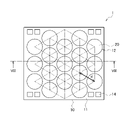
- FIG. 1 is a plan view of the transducer of this embodiment.
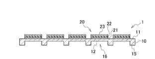
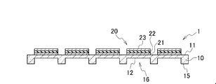
- FIG. 2 is a cross-sectional view of the transducer of this embodiment.
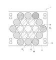
- FIG. 3 is a plan view showing the arrangement of vibrating films on the main surface of the substrate of the transducer of this embodiment.
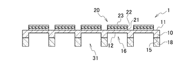
- FIG. 4 is a cross-sectional view of the transducer of the first modification.
- FIG. 5 is a cross-sectional view of a transducer of a second modification.
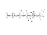
- FIG. 6 is a cross-sectional view of a transducer of a third modification.
- FIG. 7 is a plan view of a transducer of a fourth modification.
- FIG. 8 is a cross-sectional view of a transducer of a fourth modification.
- FIG. 1 is a plan view of the transducer of this embodiment.
- FIG. 2 is a cross-sectional view of the transducer of this embodiment.
- FIG. 3 is a plan view showing the arrangement of vibrating films on the main surface
- FIG. 9 is a plan view showing the arrangement of vibrating membranes on the main surface of the substrate of the transducer of the fourth modification.
- FIG. 10 is a plan view of the transducer of the fifth modification.
- FIG. 11 is a cross-sectional view of the transducer of the fifth modification.
- FIG. 12 is a plan view showing the arrangement of vibrating membranes on the main surface of the substrate of the transducer of the fifth modification.
- FIG. 13 is a plan view of the transducer of the sixth modification.
- FIG. 14 is a cross-sectional view of a transducer of a sixth modification.
- FIG. 15 is a plan view showing the arrangement of vibrating membranes on the main surface of the substrate of the transducer of the sixth modification.
- FIG. 16 is a block diagram of an electronic device.
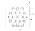
- FIG. 17 is a plan view of a transducer array.
- FIG. 18 is a cross-sectional view of a transducer array.
- FIG. 19 is a plan
- transducer It is assumed that the transducer of this embodiment is manufactured using MEMS technology and used as a speaker that generates sound waves.
- the transducer of this embodiment has the following configuration.
- the transducer has a substrate having a main surface and a back surface facing the surface, and a plurality of recesses formed in the back surface so that the main surface can vibrate in the thickness direction of the substrate, and the substrate is formed to a predetermined thickness from the main surface. and a plurality of drive layers stacked on the plurality of diaphragms such that the piezoelectric layer is sandwiched between the pair of electrode layers on the main surface, and the plurality of diaphragms are arranged in the plane of the main surface. includes vibrating membranes arranged at predetermined intervals in at least two directions. By arranging the vibrating membrane so that it occupies most of the main surface, the volume generated by the transducer can be ensured.
- the vibrating membranes arranged at predetermined intervals in at least two directions may include vibrating membranes arranged at equal intervals in three directions including the at least two directions in the plane of the main surface.
- the plurality of vibrating membranes may include vibrating membranes arranged such that the intervals between adjacent vibrating membranes are equal in the plane of the main surface.
- the natural frequencies of the multiple vibrating membranes may be higher than the audible range. Since the natural frequency is not in the frequency range of the audible range, deterioration of sound quality due to the natural frequency of the vibrating membrane does not occur in the audible range.
- the plurality of vibrating membranes may include vibrating membranes having the same shape in the plane of the main surface. Transducer design, manufacture, etc. can be facilitated.
- Wiring may be connected to a pair of electrode layers of the plurality of drive layers from electrode pads supplied with a voltage for driving the drive layers.
- the plurality of drive layers are driven by voltages supplied from wirings connected to the pair of electrode layers.
- the wiring may include wiring common to a pair of electrode layers of a plurality of drive layers. Drive layers connected to a common wire can be driven synchronously.
- the plurality of vibrating membranes may include vibrating membranes each having an equal distance from one vibrating membrane in the plane of the main surface. By arranging the vibrating membranes so that the intervals with respect to one reference vibrating membrane are equal, the density of the vibrating membranes can be ensured and arranged.
- the vibrating membranes that are equally spaced from one vibrating membrane may be arranged at predetermined intervals along the circumference of the one vibrating membrane at predetermined intervals.
- the plurality of vibrating membranes can be arranged so that one vibrating membrane that serves as a reference is surrounded by the first round of vibrating membranes.
- One vibrating membrane and a predetermined interval, outside the first round (n-th round: n 1, 2, 3 . . . ) along which the vibrating membranes are arranged at predetermined intervals.
- a vibrating membrane may be arranged at a predetermined interval along the second circumference (the (n+1)th circumference) at a predetermined interval from the vibrating membrane.
- the plurality of vibrating membranes may include vibrating membranes having the same shape for each circumference in the plane of the main surface.
- the characteristics of the vibrating membrane can be set for each circumference.
- the wiring may include wiring that is common to the vibrating membranes arranged along each circumference.
- the driving layers on each circumference connected to the common wiring can be driven synchronously.
- a partition wall may be formed on the back surface for forming an independent space from the back surface to a predetermined height in the concave portion for each of the plurality of vibrating membranes. It is possible to reduce the deterioration of sound quality by suppressing the diffraction of the sound waves emitted from the plurality of vibrating membranes to the rear side toward the main surface side.
- a partition wall may be formed on the main surface for forming an independent space from the main surface to a predetermined height for each of the plurality of vibrating membranes. The sound emitted from the plurality of vibrating membranes on the main surface can be efficiently emitted toward the front of the main surface.
- the substrate may be composed of a silicon substrate.
- Transducers can be made using MEMS technology.
- Other substrates can support the substrate, form cavities on the back side of the substrate, and provide various functions.
- FIG. 1 is a plan view showing the transducer 1 of this embodiment.
- FIG. 2 is a cross-sectional view showing the transducer 1 of this embodiment.
- the cross-sectional view of FIG. 2 shows a cross-section taken along line II--II in the plan view of FIG.
- the transducer 1 of this embodiment is formed on a substrate 10 having a flat main surface 11 and a back surface 15 opposite the main surface 11 .
- the substrate 10 is a substantially plate-shaped silicon substrate having a predetermined thickness, and has a substantially rectangular shape with substantially equal sizes in the vertical direction and the horizontal direction in a plan view.
- the substrate 10 is not limited to a silicon substrate, and may be made of other types of materials such as a glass substrate and an organic material.
- a plurality of recesses 16 are formed on the back surface 15 of the substrate 10 .
- a plurality of recesses 16 are formed to reach a predetermined depth from main surface 11 and leave substrate 10 with a predetermined thickness so that main surface 11 can vibrate in the thickness direction of substrate 10 .
- a plurality of vibrating membranes 12 are formed in the portions where the substrate 10 having the predetermined thickness is left. Since the plurality of vibrating membranes 12 are used to generate sound waves for the speaker, their natural frequencies are higher than the audible range.
- the main surface 11 of the substrate 10 forming the plurality of diaphragms 12 is connected along the entire circumference of each diaphragm 12.
- the substrates 10 are arranged such that the diaphragms 12 have a cantilever or double-supported beam structure.
- a suitable slit may be formed in 10 .
- the driving layer 20 is laminated with the piezoelectric layer 22 sandwiched between a pair of electrode layers of a lower electrode layer 21 and an upper electrode layer 23 .
- the drive layer 20 constitutes a piezoelectric element that drives the vibration film 12 to vibrate in the thickness direction of the substrate 10 by a voltage supplied by a wiring layer (not shown).
- the plurality of vibrating membranes 12 have a substantially disk-like shape with the same diameter.
- the driving layer 20 laminated on the plurality of vibrating membranes 12 also has a substantially disk-like shape on the main surface 11 in accordance with the shape of the plurality of vibrating membranes 12 .
- a plurality of vibrating membranes 12 are arranged on the main surface 11 at equal intervals d in three directions.
- the interval d between the vibrating membranes 12 means the distance between the respective centers of the vibrating membranes 12 having a substantially disk-like shape.
- the spacing d of the vibrating membranes 12 may be the distance between the centers of gravity of the vibrating membranes 12 on the main surface 11 .
- the plurality of vibrating membranes 12 are arranged at equal intervals d in three directions, so that the other vibrating membranes 12 adjacent to each vibrating membrane 12 are located at six-fold rotational symmetry of the vibrating membrane 12 . It has symmetry to be arranged.
- the equal interval d is not limited to a strictly equal interval, and includes a case where, for example, the difference is within about ⁇ 10%, which can be regarded as substantially equal.
- FIG. 3 is a plan view showing the arrangement of vibrating membrane 12 on main surface 11 of substrate 10 of transducer 1 .
- One vibrating membrane 12 placed in the center of the main surface 11 will be referred to as a central vibrating membrane 120 .
- the plurality of vibrating membranes 12 are adjacent to the central vibrating membrane 120 and are arranged at predetermined intervals on the periphery at predetermined intervals from the central vibrating membrane 120 so as to surround the central vibrating membrane 120 . of vibrating membrane 12 .
- These six vibrating membranes 12 are referred to as the vibrating membranes 121 of the first round.
- the plurality of vibrating membranes 12 are arranged such that six vibrating membranes 12 are arranged at six-fold rotationally symmetrical positions around the first round vibrating membrane 12 1 . It has 12 vibrating membranes 12 arranged so as to surround 12 . Of these 12 vibrating membranes 12, the six vibrating membranes 12 having relatively small distances from the central vibrating membrane 120 are referred to as second round vibrating membranes 122 , and are called the central vibrating membrane 120 . The six vibrating membranes 12 with relatively large intervals are called the vibrating membranes 123 of the third circumference.
- the vibrating membrane 12-2 of the second circumference is arranged at a predetermined interval on the circumference from the central vibrating membrane 12-0 so as to surround the vibrating membrane 12-1 of the first circumference.
- the vibrating membrane 12-3 of the third circumference is arranged at a predetermined distance from the central vibrating membrane 12-0 so as to surround the vibrating membrane 12-2 of the second circumference.
- Most of the main surface 11 is occupied by a central diaphragm 12 0 , a first circumferential diaphragm 12 1 , a second circumferential diaphragm 12 2 and a third circumferential diaphragm 12 3 .
- a plurality of electrodes are arranged along a pair of sides extending in the longitudinal direction of the main surface 11 in portions where the vibrating film 12 is not arranged near the four vertexes of the main surface 11 having a substantially rectangular shape in a plan view.
- a pad 14 is formed. From the plurality of electrode pads 14, a pair of electrode layers of the lower electrode layer 21 and the upper electrode layer 23 of the driving layer 20 are connected so that voltage can be supplied to the plurality of driving layers 20 that respectively drive the plurality of vibrating membranes 12. Wiring (not shown) is connected to each. A common wiring is connected from the plurality of electrode pads 14 toward the plurality of drive layers 20 .
- the wiring connection from the pair of electrode pads 14 to the plurality of drive layers 20 is not limited to this. may be For example, each of the central vibrating membrane 12 0 , the first round vibrating membrane 12 1 , the second round vibrating membrane 12 2 and the third round vibrating membrane 12 2 arranged on the main surface 11 is driven.
- the wiring toward the driving layer 20 is common, and the central vibrating membrane 12 0 , the first round vibrating membrane 12 1 , the second round vibrating membrane 12 2 and the third round vibrating membrane 12 2 are independently connected.
- the wires directed to the driving layer 20 for driving the diaphragms 12 of the plurality of diaphragms 12 arranged on the main surface 11 may be independent and connected so that the diaphragms 12 can be individually driven.
- the vibrating membranes 12 having a substantially disk-like shape and having the same diameter are arranged on the main surface 11 at equal intervals d in three directions. Most of it is occupied by a plurality of vibrating membranes 12 .
- the vibrating membranes 12 can be arranged at positions where the adjacent vibrating membranes are 6-fold rotationally symmetrical, and can be arranged at a high density. Therefore, most of main surface 11 is effectively used as vibrating membrane 12, and transducer 1 can generate sound volume sufficient for use as a speaker.
- the transducer 1 of the present embodiment is manufactured using the MEMS technology to which the semiconductor manufacturing technology is applied, a plurality of individual pieces can be manufactured at once with high accuracy.
- the plurality of vibrating membranes 12 on the main surface 11 are arranged at equal intervals in three directions. They may be arranged at intervals. Even in such a case, the density of the plurality of vibrating membranes 12 can be ensured on the main surface 11 , and the plurality of vibrating membranes 12 can be formed on most of the main surface 11 .
- the plurality of vibrating membranes 12 are composed of a central vibrating membrane 12 0 , a first vibrating membrane 12 1 , a second vibrating membrane 12 2 and a third vibrating membrane 12 2 . 12 and 3 , the vibration membrane 12 is not limited to this, and the plurality of vibration membranes 12 may be configured from the vibration membrane 120 at the center to the vibration membranes 12 at desired circumferences.
- the plurality of vibrating membranes 12 arranged on main surface 11 are assumed to have a substantially disk-like shape with the same diameter, but the present invention is not limited to this.
- the plurality of vibrating membranes 12 may have the same predetermined shape, at least some of them may have the same shape, or all of them may have different shapes.
- the vibrating membranes 12-0 forming the respective circumferences, such as the central vibrating membrane 12-0 , the first vibrating membrane 12-1 , the second vibrating membrane 12-2 , and the third vibrating membrane 12-3 may each have the same shape.
- the central vibrating membrane 12 0 , the first round vibrating membrane 12 1 , the second round vibrating membrane 12 2 , and the third round vibrating membrane 12 3 have substantially disk-like shapes with different diameters.
- the plurality of driving layers 20 are laminated on the plurality of vibrating membranes 12, they may have the same shape as each of the plurality of vibrating membranes 12 to be laminated.
- FIG. 4 is a cross-sectional view showing the transducer 1 of the first modified example.
- the transducer 1 of the first modification has a lower partition wall 18 formed from the back surface 15 to a predetermined height so as to surround a plurality of concave portions 16 formed in the back surface 15 of the substrate 10.
- the same reference numerals are given to the corresponding members to clarify the correspondence.
- a plurality of recesses 16 are formed on the back surface 15 of the substrate 10 .
- a plurality of recesses 16 are formed to reach a predetermined depth from main surface 11 and leave substrate 10 with a predetermined thickness so that main surface 11 can vibrate in the thickness direction of substrate 10 .
- a plurality of vibrating membranes 12 are formed in the portions where the substrate 10 having the predetermined thickness is left.
- a lower partition wall 18 is formed on the back surface 15 to a predetermined height from the back surface 15 so as to surround each of the recesses 16 .
- the lower partition 18 forms a lower chamber 31 extending from the vibrating membrane 12 formed on the bottom surface of each of the recesses 16 to the top of the lower partition 18 at a predetermined height from the back surface 15 . Sound waves emitted from the vibrating membrane 12 formed on the bottom surface of the plurality of recesses 16 toward the back surface 15 are guided toward the lower chamber 31 formed by the lower partition wall 18 .
- the lower partition 18 is formed so as to surround each of the plurality of recesses 16 on the rear surface 15, the lower partition 18 is not limited to this and may be formed so as to collectively surround several recesses 16 on the rear surface 15.
- the central vibrating membrane 12 0 , the first vibrating membrane 12 1 , the second vibrating membrane 12 2 and the third vibrating membrane 12 3 shown in FIG. 12 0 , the first round vibrating membrane 12 1 , the second round vibrating membrane 12 2 and the third round vibrating membrane 12 3 may each form a common lower chamber 31 .
- the lower partition wall 18 formed along the outer periphery of the back surface 15 so as to surround all the recesses 16 in the back surface 15 may form one common lower chamber 31 .
- the sound waves emitted from the vibrating membranes 12 formed on the bottom surfaces of the plurality of recesses 16 toward the back surface 15 are guided by the lower partition wall 18 toward the lower chamber 31 and then toward the main surface 11 . diffraction is suppressed, and deterioration of sound quality caused by the diffraction is reduced.
- the lower partition wall 18 may be produced by attaching a silicon substrate having a predetermined thickness with transmission holes formed at predetermined positions to the rear surface 15 of the substrate 10 .
- the lower partition wall 18 is not limited to a silicon substrate, and may be made of other types of materials such as a glass substrate and an organic material. Alternatively, one silicon substrate may be prepared and the lower partition wall 18 and the recess 16 may be continuously formed by etching.
- FIG. 5 is a cross-sectional view showing the transducer 1 of the second modification.
- the transducer 1 of the second modification has an upper partition wall 19 extending from the main surface 11 to a predetermined height so as to surround a plurality of vibrating films 12 formed on the main surface 11 of the substrate 10 . is formed. Since other configurations are the same as those of the transducer 1 of this embodiment, the same reference numerals are given to the corresponding members to clarify the correspondence.
- a plurality of recesses 16 are formed on the back surface 15 of the substrate 10 .
- a plurality of recesses 16 are formed to reach a predetermined depth from main surface 11 and leave substrate 10 with a predetermined thickness so that main surface 11 can vibrate in the thickness direction of substrate 10 .
- a plurality of vibrating membranes 12 are formed in the portions where the substrate 10 having the predetermined thickness is left.
- An upper partition wall 19 is formed on the main surface 11 to a predetermined height from the main surface 11 so as to surround each of the plurality of diaphragms 12 and the plurality of drive layers 20 laminated on the plurality of diaphragms 12 .
- the upper partition 19 forms an upper chamber 32 for each of the plurality of vibrating membranes 12 from the vibrating membrane 12 on the main surface 11 to the top of the upper partition 19 at a predetermined height. Sound waves emitted from the vibrating membrane 12 on the main surface 11 are directed toward the upper chamber 32 by the upper partition 19 . Therefore, sound waves emitted from the plurality of vibrating membranes 12 on main surface 11 are efficiently emitted toward the front of main surface 11 .
- the upper partition 19 is formed so as to surround each of the plurality of vibrating membranes 12 on the main surface 11, the upper partition 19 is not limited to this and may collectively surround several vibrating membranes 12 on the main surface 11. It may be formed as For example, the central vibrating membrane 12 0 , the first vibrating membrane 12 1 , the second vibrating membrane 12 2 and the third vibrating membrane 12 3 shown in FIG. 12 0 , the first round vibrating membrane 12 1 , the second round vibrating membrane 12 2 and the third round vibrating membrane 12 3 may each form a common upper chamber 32 . Also, the upper partition 19 formed along the outer periphery of the main surface 11 so as to surround all the vibrating membranes 12 on the main surface 11 may form one common upper chamber 32 . Even in such a case, the sound waves emitted from the plurality of vibrating membranes 12 are guided toward the upper chamber 32 formed by the upper partition wall 19 and efficiently emitted toward the front of the main surface 11 .
- the upper partition wall 19 may be produced by attaching a silicon substrate having a predetermined thickness with transmission holes formed at predetermined positions to the main surface 11 of the substrate 10 .
- the upper partition wall 19 is not limited to a silicon substrate, and may be made of other types of materials such as a glass substrate and an organic material. Alternatively, one silicon substrate may be prepared and the upper partition wall 19 may be formed by etching.
- the upper partition wall 19 is formed up to a predetermined height from the main surface 11 so as to surround the plurality of diaphragms 12 formed on the main surface 11 of the substrate 10.
- a lower partition wall 18 may be further formed up to a predetermined height from the back surface 15 so as to surround the plurality of recesses 16 formed in the bottom wall.
- FIG. 6 is a cross-sectional view showing the transducer 1 of the third modification.
- the transducer 1 of the third modification has a side wall 51 formed to a predetermined height along the outer periphery of the back surface 15 of the substrate 10, and attached to the top of the side wall 51, The difference is that it has a second substrate 52 having a substantially rectangular shape similar to that of the substrate 10 in plan view. Since other configurations are the same as those of the transducer 1 of this embodiment, the same reference numerals are given to the corresponding members to clarify the correspondence.
- a plurality of recesses 16 are formed on the back surface 15 of the substrate 10 .
- a plurality of recesses 16 are formed to reach a predetermined depth from main surface 11 and leave substrate 10 with a predetermined thickness so that main surface 11 can vibrate in the thickness direction of substrate 10 .
- a plurality of vibrating membranes 12 are formed in the portions where the substrate 10 having the predetermined thickness is left.
- a side wall 51 having a predetermined thickness is formed inside the rear surface 15 along the outer periphery to a predetermined height from the rear surface 15 .
- a second substrate 52 having a substantially rectangular shape similar to that of the substrate 10 in plan view is attached to the top of the side wall 51 having a predetermined height from the rear surface 15 .
- a closed cavity 33 is formed in the rear surface 15 of the substrate 10 by the sidewalls 51 and the second substrate 52 .
- the side wall 51 may be produced by attaching a silicon frame member having a predetermined thickness with transmission holes formed at predetermined positions to the back surface 15 of the substrate 10 .
- the sidewalls 51 are not limited to silicon, and may be made of other types of materials such as glass and organic materials. Alternatively, one silicon substrate may be prepared and the side wall 51 and the concave portion 16 may be continuously formed by etching.
- the second substrate 52 may be a silicon substrate like the substrate 10, may be made of other types of materials such as glass and organic materials, or may be a printed circuit board.
- the back surface 15 of the substrate 10 is formed with the cavity 33 sealed by the side walls 51 and the second substrate 52
- the present invention is not limited to this, and the cavity 33 may not be sealed. may not be formed.
- the side wall 51 is formed up to a predetermined height on the back surface 15 and the second substrate 52 is attached to the top of the back surface 15.
- the present invention is not limited to this.
- the two substrates 52 may be attached to the back surface 15 by any suitable means. In such a case as well, the second substrate 52 suppresses the diffraction of sound waves emitted in the direction of the rear surface 15 from the plurality of vibrating films 12 formed on the bottom surfaces of the plurality of recesses 16 toward the main surface 11 . , providing a plurality of drive circuits for the drive layers 20 on the second substrate 52, and various other functions can be provided.
- FIG. 7 is a plan view showing the transducer 1 of the fourth modification.
- FIG. 8 is a cross-sectional view showing the transducer 1 of the fourth modification.
- the cross-sectional view of FIG. 8 shows a cross-section taken along line VIII-VIII in the plan view of FIG.
- the transducer 1 of the fourth modification differs from the transducer 1 of the present embodiment in the arrangement of the plurality of vibrating membranes 12 and the plurality of electrode pads 14 on the main surface 11 of the substrate 10 . Since other configurations are the same as those of the transducer 1 of this embodiment, the same reference numerals are given to the corresponding members to clarify the correspondence.
- a transducer 1 of the fourth modification is formed on a substrate 10 having a flat main surface 11 and a back surface 15 facing the main surface 11 .
- the substrate 10 is a substantially plate-shaped silicon substrate having a predetermined thickness, and has a substantially rectangular shape with substantially equal sizes in the vertical direction and the horizontal direction in a plan view.
- the substrate 10 is not limited to silicon, and may be made of other types of materials such as a glass substrate and an organic material.
- a plurality of recesses 16 are formed on the back surface 15 of the substrate 10 .
- a plurality of recesses 16 are formed to reach a predetermined depth from main surface 11 and leave substrate 10 with a predetermined thickness so that main surface 11 can vibrate in the thickness direction of substrate 10 .
- a plurality of vibrating membranes 12 are formed in the portions where the substrate 10 having the predetermined thickness is left. Since the plurality of vibrating membranes 12 are used to generate sound waves for the speaker, their natural frequencies are higher than the audible range.
- the main surface 11 of the substrate 10 forming the plurality of diaphragms 12 is connected along the entire circumference of each diaphragm 12.
- the substrates 10 are arranged such that the diaphragms 12 have a cantilever or double-supported beam structure.
- a suitable slit may be formed in 10 .
- the driving layer 20 is laminated with the piezoelectric layer 22 sandwiched between a pair of electrode layers of a lower electrode layer 21 and an upper electrode layer 23 .
- the drive layer 20 constitutes a piezoelectric element that drives the vibration film 12 to vibrate in the thickness direction of the substrate 10 by a voltage supplied by a wiring layer (not shown).
- the plurality of vibrating membranes 12 have a substantially disk-like shape with the same diameter.
- the driving layer 20 laminated on each vibrating membrane 12 also has a substantially disk-like shape in accordance with the shape of the plurality of vibrating membranes 12 .
- a plurality of vibrating membranes 12 are arranged on the main surface 11 at equal intervals d in three directions. Therefore, the plurality of vibrating membranes 12 have symmetry such that the other vibrating membranes 12 adjacent to each vibrating membrane 12 are arranged at six-fold rotation symmetrical positions of the vibrating membrane 12 .
- the equal interval d is not limited to a strictly equal interval, and includes a case where, for example, the difference is within about ⁇ 10%, which can be regarded as substantially equal.
- FIG. 9 is a plan view showing the arrangement of vibrating membrane 12 on main surface 11 of substrate 10 of transducer 1 .
- One vibrating membrane 12 placed in the center of the main surface 11 will be referred to as a central vibrating membrane 120 .
- the plurality of vibrating membranes 12 are adjacent to the central vibrating membrane 120 and are arranged at predetermined intervals on the periphery at predetermined intervals from the central vibrating membrane 120 so as to surround the central vibrating membrane 120 . of vibrating membrane 12 .
- These six vibrating membranes 12 are referred to as the vibrating membranes 121 of the first round.
- the plurality of vibrating membranes 12 surround the first round vibrating membrane 12 such that adjacent vibrating membranes 12 are arranged at six-fold rotation symmetrical positions around the first round vibrating membrane 12 1 .
- It has ten vibrating membranes 12 arranged as follows. Among these ten vibrating membranes 12, six vibrating membranes 12 having relatively small distances from the center vibrating membrane 120 are referred to as second round vibrating membranes 122 , and are referred to as the central vibrating membrane 120.
- the four vibrating membranes 12 having a relatively large interval between them are referred to as the vibrating membranes 123 of the third circumference.
- the vibrating membrane 12-2 of the second circumference is arranged at a predetermined interval on the circumference from the central vibrating membrane 12-0 so as to surround the vibrating membrane 12-1 of the first circumference.
- the vibrating membrane 12-3 of the third circumference is arranged at a predetermined distance from the central vibrating membrane 12-0 so as to surround the vibrating membrane 12-2 of the second circumference.
- Most of the main surface 11 is occupied by a central diaphragm 12 0 , a first circumferential diaphragm 12 1 , a second circumferential diaphragm 12 2 and a third circumferential diaphragm 12 3 .
- a plurality of electrodes are arranged along a pair of laterally extending sides of the main surface 11 in portions where the vibrating membrane 12 is not arranged near the four vertexes of the main surface 11 having a substantially rectangular shape in a plan view.
- a pad 14 is formed. From the plurality of electrode pads 14, a pair of electrode layers of the lower electrode layer 21 and the upper electrode layer 23 of the driving layer 20 are connected so that voltage can be supplied to the plurality of driving layers 20 that respectively drive the plurality of vibrating membranes 12. Wiring (not shown) is connected to each. A common wiring is connected from the plurality of electrode pads 14 toward the plurality of drive layers 20 .
- the wiring connection from the pair of electrode pads 14 to the plurality of drive layers 20 is not limited to this. may be For example, each of the central vibrating membrane 12 0 , the first round vibrating membrane 12 1 , the second round vibrating membrane 12 2 and the third round vibrating membrane 12 2 arranged on the main surface 11 is driven.
- the wiring directed to the driving layer 20 may be common, and may be connected so that they can be driven independently.
- the wires directed to the driving layer 20 for driving the diaphragms 12 of the plurality of diaphragms 12 arranged on the main surface 11 may be independent and connected so that the diaphragms 12 can be individually driven.
- the vibrating membranes 12 having a substantially disk-like shape and having the same diameter are arranged on the main surface 11 at equal intervals d in three directions. Most of it is occupied by a plurality of vibrating membranes 12 .
- the vibrating membranes 12 can be arranged at positions where the adjacent vibrating membranes are 6-fold rotationally symmetrical, and can be arranged at a high density. Therefore, most of main surface 11 is effectively used as vibrating membrane 12, and transducer 1 can generate sound volume sufficient for use as a speaker.
- the transducer 1 of the fourth modification is manufactured using the MEMS technology to which the semiconductor manufacturing technology is applied, it is possible to manufacture a plurality of individual pieces at once with high accuracy.
- FIG. 10 is a plan view showing the transducer 1 of the fifth modified example.
- FIG. 11 is a cross-sectional view showing the transducer 1 of the fifth modified example.
- the cross-sectional view of FIG. 11 shows a cross-section taken along line XI--XI in the plan view of FIG.
- the transducer 1 of the fifth modification differs from the transducer 1 of this embodiment in the arrangement of the plurality of vibrating membranes 12 and the plurality of electrode pads 14 on the main surface 11 of the substrate 10 . Since other configurations are the same as those of the transducer 1 of this embodiment, the same reference numerals are given to the corresponding members to clarify the correspondence.
- a transducer 1 of the fifth modification is formed on a substrate 10 having a flat main surface 11 and a back surface 15 facing the main surface 11 .
- the substrate 10 is a substantially plate-shaped silicon substrate having a predetermined thickness, and has a substantially rectangular shape with substantially equal sizes in the vertical direction and the horizontal direction in a plan view.
- the substrate 10 is not limited to a silicon substrate, and may be made of other types of materials such as a glass substrate and an organic material.
- a plurality of recesses 16 are formed on the back surface 15 of the substrate 10 .
- a plurality of recesses 16 are formed to reach a predetermined depth from main surface 11 and leave substrate 10 with a predetermined thickness so that main surface 11 can vibrate in the thickness direction of substrate 10 .
- a plurality of vibrating membranes 12 are formed in the portions where the substrate 10 having the predetermined thickness is left. Since the plurality of vibrating membranes 12 are used to generate sound waves for the speaker, their natural frequencies are higher than the audible range.
- the main surface 11 of the substrate 10 forming the plurality of diaphragms 12 is connected along the entire circumference of each diaphragm 12.
- the substrates 10 are arranged such that the diaphragms 12 have a cantilever or double-supported beam structure.
- a suitable slit may be formed in 10 .
- the driving layer 20 is laminated with the piezoelectric layer 22 sandwiched between a pair of electrode layers of a lower electrode layer 21 and an upper electrode layer 23 .
- the drive layer 20 constitutes a piezoelectric element that drives the vibration film 12 to vibrate in the thickness direction of the substrate 10 by a voltage supplied by a wiring layer (not shown).
- the plurality of vibrating membranes 12 have a substantially disk-like shape with the same diameter.
- the driving layer 20 laminated on the plurality of vibrating membranes 12 also has a substantially disk-like shape on the main surface 11 in accordance with the shape of the plurality of vibrating membranes 12 .
- the plurality of vibrating membranes 12 include vibrating membranes 12 arranged at equal intervals d in three directions on the main surface 11 .
- the interval d between the vibrating membranes 12 means the distance between the respective centers of the vibrating membranes 12 having a substantially disk-like shape.
- the spacing d of the vibrating membranes 12 may be the distance between the centers of gravity of the vibrating membranes 12 on the main surface 11 .
- the equal interval d is not limited to a strictly equal interval, and includes a case where, for example, the difference is within about ⁇ 10%, which can be regarded as substantially equal.
- FIG. 12 is a plan view showing the arrangement of vibrating membrane 12 on main surface 11 of substrate 10 of transducer 1 .
- One vibrating membrane 12 placed in the center of the main surface 11 will be referred to as a central vibrating membrane 120 .
- the plurality of vibrating membranes 12 are adjacent to the central vibrating membrane 120 and are arranged at predetermined intervals on the periphery at predetermined intervals from the central vibrating membrane 120 so as to surround the central vibrating membrane 120 . of vibrating membrane 12 .
- These six vibrating membranes 12 are referred to as the vibrating membranes 121 of the first round.
- the vibrating membrane 12-1 of the first circumference has a symmetry of being arranged at positions with 6-fold rotational symmetry around the central vibrating membrane 12-0 .
- the plurality of vibrating membranes 12 has ten vibrating membranes 12 arranged so as to surround the vibrating membrane 121 of the first circumference. These vibrating membranes 12 are referred to as second round vibrating membranes 122 .
- the second circumferential vibrating membranes 12 2 are arranged in a substantially rectangular shape in plan view from the central vibrating membrane 12 0 , and five on each side near the vertical sides of the main surface 11 are arranged from the central vibrating membrane 12 0 . They are arranged at predetermined intervals on the circumference of predetermined intervals.
- the vibrating films 12 at the center and both ends are arranged at six-fold rotational symmetry with respect to the first round vibrating film 121 , respectively.
- Most of the main surface 11 is occupied by a central diaphragm 12 0 , a first circumferential diaphragm 12 1 and a second circumferential diaphragm 12 2 .
- a plurality of electrodes are arranged along a pair of sides extending in the longitudinal direction of the main surface 11 in portions where the vibrating film 12 is not arranged near the four vertexes of the main surface 11 having a substantially rectangular shape in a plan view.
- a pad 14 is formed. From the plurality of electrode pads 14, a pair of electrode layers of the lower electrode layer 21 and the upper electrode layer 23 of the driving layer 20 are connected so that voltage can be supplied to the plurality of driving layers 20 that respectively drive the plurality of vibrating membranes 12. Wiring (not shown) is connected to each. A common wiring is connected from the plurality of electrode pads 14 toward the plurality of drive layers 20 .
- the wiring connection from the pair of electrode pads 14 to the plurality of drive layers 20 is not limited to this. may be For example, for each of the central vibrating membrane 12 0 , the first vibrating membrane 12 1 , and the second vibrating membrane 12 2 arranged on the main surface 11, there are wirings directed to the driving layer 20 that drives the vibrating membrane 12.
- the vibrating membrane 12 0 in the center, the vibrating membrane 12 1 in the first round, and the vibrating membrane 12 2 in the second round may be connected so that they can be driven independently.
- the wires directed to the driving layer 20 for driving the diaphragms 12 of the plurality of diaphragms 12 arranged on the main surface 11 may be independent and connected so that the diaphragms 12 can be individually driven.
- the plurality of vibrating membranes 12 have disk-like shapes with the same diameter on the main surface 11 .
- the plurality of vibrating membranes 12 are divided into three vibrating membranes 12 arranged at equal intervals d in three directions, and the vibrating membranes 12 arranged at predetermined intervals on the periphery at predetermined intervals from the center vibrating membrane 120 . contains.
- most of the main surface 11 is occupied by the plurality of vibrating membranes 12 . Therefore, most of main surface 11 is effectively used as vibrating membrane 12, and transducer 1 can generate sound volume sufficient for use as a speaker.
- the transducer 1 of the fifth modification is manufactured using the MEMS technology to which the semiconductor manufacturing technology is applied, it is possible to manufacture a plurality of individual pieces at once with high accuracy.
- FIG. 13 is a plan view showing the transducer 1 of the sixth modification.
- FIG. 14 is a cross-sectional view showing the transducer 1 of the sixth modification.
- the cross-sectional view of FIG. 14 shows a cross-section taken along line XIV-XIV in the plan view of FIG.
- the transducer 1 of the sixth modification differs from the transducer 1 of this embodiment in the arrangement of the plurality of vibrating membranes 12 and the plurality of electrode pads 14 on the main surface 11 of the substrate 10 . Since other configurations are the same as those of the transducer 1 of this embodiment, the same reference numerals are given to the corresponding members to clarify the correspondence.
- a transducer 1 of the sixth modification is formed on a substrate 10 having a flat main surface 11 and a back surface 15 facing the main surface 11 .
- the substrate 10 is a substantially plate-shaped silicon substrate having a predetermined thickness, and has a substantially rectangular shape with substantially equal sizes in the vertical direction and the horizontal direction in a plan view.
- the substrate 10 is not limited to a silicon substrate, and may be made of other types of materials such as a glass substrate and an organic material.
- a plurality of recesses 16 are formed on the back surface 15 of the substrate 10 .
- a plurality of recesses 16 are formed to reach a predetermined depth from main surface 11 and leave substrate 10 with a predetermined thickness so that main surface 11 can vibrate in the thickness direction of substrate 10 .
- a plurality of vibrating membranes 12 are formed in the portions where the substrate 10 having the predetermined thickness is left. Since the plurality of vibrating membranes 12 are used to generate sound waves for the speaker, their natural frequencies are higher than the audible range.
- the main surface 11 of the substrate 10 forming the plurality of diaphragms 12 is connected along the entire circumference of each diaphragm 12.
- the substrates 10 are arranged such that the diaphragms 12 have a cantilever or double-supported beam structure.
- a suitable slit may be formed in 10 .
- the driving layer 20 is laminated with the piezoelectric layer 22 sandwiched between a pair of electrode layers of a lower electrode layer 21 and an upper electrode layer 23 .
- the drive layer 20 constitutes a piezoelectric element that drives the vibration film 12 to vibrate in the thickness direction of the substrate 10 by a voltage supplied by a wiring layer (not shown).
- the plurality of vibrating membranes 12 have a substantially disk-like shape with the same diameter.
- the driving layer 20 laminated on each vibrating membrane 12 also has a substantially disk-like shape in accordance with the shape of the plurality of vibrating membranes 12 .
- the plurality of vibrating membranes 12 includes vibrating membranes 12 arranged at equal intervals in two substantially orthogonal directions on main surface 11 . That is, the distance d1 in the vertical direction and the distance d2 in the horizontal direction of the main surface 11, which is substantially rectangular in plan view.
- the interval between the vibrating membranes 12 means the distance between the respective centers of the vibrating membranes 12 having a substantially disk-like shape.
- the spacing of the vibrating membranes 12 may be the distance between the respective centers of gravity of the vibrating membranes 12 on the main surface 11 .
- the equal spacing between the vertical spacing d1 and the horizontal spacing d2 is not limited to strictly equal spacing, but includes cases where the difference can be considered to be substantially equal, such as a difference of about ⁇ 10%.
- FIG. 15 is a plan view showing the arrangement of vibrating membrane 12 on main surface 11 of substrate 10 of transducer 1 .
- main surface 11 which is substantially rectangular in plan view, four vibrating membranes 12 are arranged in the vertical direction near the left side in the figure at intervals d1 . These four vibrating membranes 12 will be referred to as a first row of vibrating membranes 121 .
- a second row of diaphragms 12.sub.2, a third row of diaphragms 12.sub.3 , and a fourth row of diaphragms 12.sub.4 which are similarly arranged in the vertical direction, are arranged in the horizontal direction. are arranged near the right side of the figure.
- Most of the main surface 11 is occupied by a first row of diaphragm 12 1 , a second row of diaphragm 12 2 , a third row of diaphragm 12 3 and a fourth row of diaphragm 12 4 .
- a plurality of electrodes are arranged along a pair of laterally extending sides of the main surface 11 in portions where the vibrating membrane 12 is not arranged near the four vertexes of the main surface 11 having a substantially rectangular shape in a plan view.
- a pad 14 is formed. From the plurality of electrode pads 14, a pair of electrode layers of the lower electrode layer 21 and the upper electrode layer 23 of the driving layer 20 are connected so that voltage can be supplied to the plurality of driving layers 20 that respectively drive the plurality of vibrating membranes 12. Wiring (not shown) is connected to each. A common wiring is connected from the plurality of electrode pads 14 toward the plurality of drive layers 20 .
- the wiring connection from the pair of electrode pads 14 to the plurality of drive layers 20 is not limited to this. may be For example, for each of the first row vibrating film 12 1 , the second row vibrating film 12 2 , the third row vibrating film 12 3 and the fourth row vibrating film 12 4 arranged on the main surface 11, the vibrating membrane 12 , and the first row vibrating film 12 1 , the second row vibrating film 12 2 , the third row vibrating film 12 3 , and the fourth row vibrating film 12 4 . may be connected so that they can be driven independently.
- the wires directed to the driving layer 20 for driving the diaphragms 12 of the plurality of diaphragms 12 arranged on the main surface 11 may be independent and connected so that the diaphragms 12 can be individually driven.
- the vibrating membranes 12 having a substantially disk-like shape and having the same diameter on the main surface 11 are arranged at intervals of d1 in the longitudinal direction and d2 in the lateral direction.
- most of main surface 11 is occupied by a plurality of vibrating membranes 12 . Therefore, most of main surface 11 is effectively used as vibrating membrane 12, and transducer 1 can generate sound volume sufficient for use as a speaker.
- the transducer 1 of the sixth modification is manufactured using the MEMS technology to which the semiconductor manufacturing technology is applied, a plurality of individual pieces can be manufactured at once with high precision.
- the electronic device of this embodiment includes the transducer 1 of this embodiment as a speaker.
- the electronic device of this embodiment can generate a sufficient sound volume by including the transducer 1 of this embodiment as a speaker.
- FIG. 16 is a block diagram showing the electronic device of this embodiment.
- the electronic device of the present embodiment includes the transducer 1 of the present embodiment described above as a speaker, and is capable of generating sound waves of constant sound quality from the transducer 1 according to the audio signal input from the signal source 41. further includes an analog-to-digital converter (ADC) 42 , a digital signal processor (DSP) 43 , a digital-to-analog converter (DAC) 44 and an amplifier 45 .
- ADC analog-to-digital converter
- DSP digital signal processor
- DAC digital-to-analog converter
- the audio signal input as an analog signal from the signal source 41 is converted into a digital signal by the analog-to-digital converter 42 and then subjected to predetermined processing by the digital signal processor 43 .
- the digital signal processor 43 compensates for the frequency characteristics of the transducers 1, controls the phases between the transducers 1, and performs equalizer, surround, and other processing as necessary.
- the audio signal processed by the digital signal processor 43 is converted to an analog signal by the digital-to-analog converter 44 and then amplified by the amplifier 45 to drive the transducer 1 .
- the electronic device of the present embodiment includes the transducer 1 of the present embodiment as a speaker, it is possible to provide a sufficient sound volume even though the speaker is small.
- the transducer 1 of the present embodiment is driven by a voltage using a piezoelectric element, power consumption can be reduced as compared with electronic equipment having a conventional dynamic speaker or the like.
- the transducer 1 provided in the electronic device is manufactured using the MEMS technology to which the semiconductor manufacturing technology is applied, it is possible to manufacture a plurality of individual pieces at once with high accuracy.
- the transducer array of this embodiment uses the transducer of this embodiment, the main surfaces of the plurality of transducers face one side, and the plurality of transducers include transducers arranged at predetermined intervals in at least two directions. are arranged two-dimensionally. Since the transducer array of this embodiment uses the transducer of this embodiment, it can generate a sufficient volume. Moreover, since the plurality of transducers are arranged at predetermined intervals in at least two directions, they can emit sound waves so that the sound volume distribution is substantially uniform in the predetermined range on the one side.
- the transducers arranged at predetermined intervals in at least two directions may include transducers arranged at equal intervals in three directions including at least two directions in the plane defined by the two-dimensional arrangement.
- each transducer of the plurality of transducers may be inclined toward the center of the plurality of transducers arranged two-dimensionally as it moves away from the center.
- the transducer array can emit sound waves to be centered on one side of the front face.
- FIG. 17 is a plan view showing the transducer array 2 of this embodiment.
- FIG. 18 is a cross-sectional view showing the transducer array 2 of this embodiment. The cross-sectional view of FIG. 18 shows a cross-section taken along line XVIII--XVIII in the plan view of FIG.
- a plurality of transducers 1 of the present embodiment are arranged on the flat main surface 61 of the support substrate 60 so that the main surface 11 faces away from the main surface 61 of the support substrate 60 . are arranged two-dimensionally in the The plurality of transducers 1 are arranged on the main surface 61 at equal intervals D in three directions, and are arranged such that the main surface 61 of the transducers 1 inclines toward the center of the support substrate 60 as they move away from the center of the support substrate 60. ing.
- the interval D between the transducers 1 may be the distance between the central positions of the outline when the transducer 1 is viewed from above, or the distance between the positions of the center of gravity of the vibrating membrane 12 formed on the main surface 61 of the transducer 1. It may be the distance between It should be noted that the equal interval D is not limited to a strictly equal interval, and includes a case where the difference can be considered to be substantially equal, such as a difference of about ⁇ 10%.
- the support substrate 60 has a substantially plate-like shape with a predetermined thickness, and has a substantially rectangular shape with substantially equal sizes in the vertical direction and the horizontal direction in a plan view.
- the support substrate 60 may be a silicon substrate like the substrate 10, may be made of other types of materials such as glass and organic materials, or may be a printed circuit board.
- the plurality of transducers 1 are arranged at equal intervals D in three directions, so that the other transducers 1 adjacent to each transducer 1 are arranged at six-fold rotation symmetrical positions of the transducer 1. have a sexuality.
- the plurality of transducers 1 has six transducers 1 arranged at six-fold rotationally symmetrical positions around the central transducer 1 adjacent to the central transducer 1 of the main surface 61 .
- 12 transducers 1 are arranged so as to surround the six transducers 1 so that the six transducers 1 are arranged at six-fold rotationally symmetrical positions around adjacent ones. has a transducer 1 of
- the main surface 61 of the transducer 1 is arranged so as to incline toward the center of the main surface 61 of the support substrate 60 as it moves away from the center.
- the normal to major surface 61 is drawn in FIG. 18 to clarify the inclination of major surface 61 .
- the transducer array 2 of the present embodiment since the transducers 1 are arranged so that the intervals D are equal, in a certain range in front of the main surface 61 of the support substrate 60, the light emitted from the plurality of transducers 1 Sound waves can have a substantially uniform volume distribution.
- the main surface 61 of the transducer 1 is inclined toward the center of the main surface 61 of the support substrate 60 as it moves away from the center, the sound waves are emitted so as to concentrate on the front center of the main surface 61 of the support substrate 60 . can be released.
- the transducer 1 of this embodiment can generate a sufficient volume as a speaker
- the transducer array 2 of this embodiment comprising a plurality of transducers 1 can also generate a sufficient volume.
- FIG. 19 is a plan view showing a transducer array 2 of a modified example.
- the transducer array 2 of the modified example differs from the transducer array 2 of the present embodiment in that the transducers 1 of the sixth modified example are used and the arrangement of the transducers 1 is different. Since other configurations are the same as those of the transducer array of this embodiment, corresponding members are given the same reference numerals to clarify the correspondence.
- the transducer 1 of the sixth modification is two-dimensionally arranged on the flat main surface 61 of the support substrate 60 such that the main surface 11 of the transducer 1 faces away from the main surface 61 of the support substrate 60 . are placed in On the main surface 61, which is substantially rectangular in plan view, five transducers 1 arranged at intervals of D1 in the longitudinal direction constitute one row of transducers 1, and seven rows of transducers 1 are arranged at intervals of D2 in the transverse direction. ing. The longitudinal direction of the transducers 1 in each row is aligned with the direction in which the row extends.
- the interval D between the transducers 1 may be the distance between the central positions of the outline when the transducer 1 is viewed from above, or the distance between the positions of the center of gravity of the vibrating membrane 12 formed on the main surface 61 of the transducer 1. It may be the distance between Most of the main surface 61 is occupied by these transducers 1 .
- Transducer 1 may be arranged such that main surface 11 inclines toward the center of support substrate 60 as it moves away from the center of support substrate 60 .
- the support substrate 60 has a substantially plate-like shape with a predetermined thickness, and has a substantially rectangular shape with substantially equal sizes in the vertical direction and the horizontal direction in a plan view.
- the support substrate 60 may be a silicon substrate like the substrate 10, may be made of other types of materials such as glass and organic materials, or may be a printed circuit board.
- the transducers 1 are arranged at regular intervals of D 1 in the vertical direction and D 2 in the horizontal direction. Therefore, in a certain range in front of the main surface 61 of the support substrate 60, the sound waves emitted from the plurality of transducers 1 can have a substantially uniform volume distribution. Further, since the transducer 1 of Modification 6 can generate sufficient volume as a speaker, the transducer array 2 of Modification including a plurality of transducers 1 can also generate sufficient volume.
- the equal spacing between the vertical spacing D1 and the horizontal spacing D2 is not limited to a strictly equal spacing, but includes a case in which the difference can be considered to be substantially equal, such as a difference of about ⁇ 10%.
- the transducer may be applied to generate ultrasonic waves in addition to generating sound waves.
- the transducer may also be applied in applications that detect sound waves or ultrasound waves.
- Transducer 2 Transducer Array 10 Substrate 11 Main Surface 12 Vibration Membrane 12 0 Center Vibration Membrane 12 1 1st Circulation Vibration Membrane, 1st Row Vibration Membrane 12 2 2nd Circumference Vibration Membrane, 2nd Row Vibration Membrane 12 3 Vibration film in third circumference, 3rd row vibration film 12 4 4th row vibration film 14 Electrode pad 15 Rear surface 16 Recess 18 Lower partition 19 Upper partition 20 Drive layer 21 Lower electrode layer 22 Piezoelectric layer 23 Upper electrode layer
Landscapes
- Engineering & Computer Science (AREA)
- Physics & Mathematics (AREA)
- Acoustics & Sound (AREA)
- Signal Processing (AREA)
- Health & Medical Sciences (AREA)
- Otolaryngology (AREA)
- Mechanical Engineering (AREA)
- Transducers For Ultrasonic Waves (AREA)
- Piezo-Electric Transducers For Audible Bands (AREA)
Abstract
Description
本実施の形態のトランスデューサは、MEMS技術を用いて製造され、音波を発生するスピーカとして使用されることを想定している。本実施の形態のトランスデューサは、次のような構成を有している。
図4は、第1変形例のトランスデューサ1を示す断面図である。第1変形例のトランスデューサ1は、本実施の形態のトランスデューサ1と比べると、基板10の背面15に形成された複数の凹部16を取り囲むように背面15から所定の高さまで下部隔壁18が形成されている点が相違している。他の構成は本実施の形態のトランスデューサ1と同様であるので、対応する部材には同一の参照番号を付して対応関係を明らかにする。
図5は、第2変形例のトランスデューサ1を示す断面図である。第2変形例のトランスデューサ1は、本実施の形態のトランスデューサ1と比べると、基板10の主表面11に形成された複数の振動膜12を取り囲むように主表面11から所定の高さまで上部隔壁19が形成されている点が相違している。他の構成は本実施の形態のトランスデューサ1と同様であるので、対応する部材には同一の参照番号を付して対応関係を明らかにする。
図6は、第3変形例のトランスデューサ1を示す断面図である。第3変形例のトランスデューサ1は、本実施の形態のトランスデューサ1と比べると、基板10の背面15に外周に沿って所定の高さまで形成された側壁51と、側壁51の頂部に取り付けられた、平面視で基板10と同様の略矩形状の形状を有する第2基板52とを有する点が相違している。他の構成は本実施の形態のトランスデューサ1と同様であるので、対応する部材には同一の参照番号を付して対応関係を明らかにする。
図7は、第4変形例のトランスデューサ1を示す平面図である。図8は、第4変形例のトランスデューサ1を示す断面図である。図8の断面図は、図7の平面図における切断線VIII-VIIIによる切断面を示している。第4変形例のトランスデューサ1は、本実施の形態のトランスデューサ1と比べると、基板10の主表面11における複数の振動膜12及び複数の電極パッド14の配置が相違している。他の構成は本実施の形態のトランスデューサ1と同様であるので、対応する部材には同一の参照番号を付して対応関係を明らかにする。
図10は、第5変形例のトランスデューサ1を示す平面図である。図11は、第5変形例のトランスデューサ1を示す断面図である。図11の断面図は、図10の平面図における切断線XI-XIによる切断面を示している。第5変形例のトランスデューサ1は、本実施の形態のトランスデューサ1と比べると、基板10の主表面11における複数の振動膜12及び複数の電極パッド14の配置が相違している。他の構成は本実施の形態のトランスデューサ1と同様であるので、対応する部材には同一の参照番号を付して対応関係を明らかにする。
図13は、第6変形例のトランスデューサ1を示す平面図である。図14は、第6変形例のトランスデューサ1を示す断面図である。図14の断面図は、図13の平面図における切断線XIV-XIVによる切断面を示している。第6変形例のトランスデューサ1は、本実施の形態のトランスデューサ1と比べると、基板10の主表面11における複数の振動膜12及び複数の電極パッド14の配置が相違している。他の構成は本実施の形態のトランスデューサ1と同様であるので、対応する部材には同一の参照番号を付して対応関係を明らかにする。
本実施の形態の電子機器は、スピーカとして本実施の形態のトランスデューサ1を備えている。本実施の電子機器は、本実施のトランスデューサ1をスピーカとして備えることにより十分な音量を発生することができる。
本実施の形態のトランスデューサアレイは、本実施の形態のトランスデューサを用い、複数のトランスデューサの主表面が一側を向き、複数のトランスデューサは、少なくとも2方向にそれぞれ所定の間隔で配置されたトランスデューサを含むように2次元状に配置されたものである。本実施の形態のトランスデューサアレイは、本実施の形態のトランスデューサを用いるため、十分な音量を発生することができる。また、複数のトランスデューサは、少なくとも2方向にそれぞれ所定の間隔で配置されているため、前記一側の所定の範囲において音量の分布が略均一になるように音波を放出することができる。
図19は、変形例のトランスデューサアレイ2を示す平面図である。変形例のトランスデューサアレイ2は、本実施の形態のトランスデューサアレイ2とは、第6変形例のトランスデューサ1を用いることと、トランスデューサ1の配置とが相違している。他の構成は本実施のトランスデューサアレイと同様であるので、対応する部材には同一の参照番号を付して対応関係を明らかにする。
2 トランスデューサアレイ
10 基板
11 主表面
12 振動膜
120 中央の振動膜
121 第1周の振動膜、第1列の振動膜
122 第2周の振動膜、第2列の振動膜
123 第3周の振動膜、第3列の振動膜
124 第4列の振動膜
14 電極パッド
15 背面
16 凹部
18 下部隔壁
19 上部隔壁
20 駆動層
21 下部電極層
22 圧電体層
23 上部電極層
Claims (20)
- 主表面及び前記主表面に対向する背面を有する基板と、
前記主表面が前記基板の厚さ方向に振動できるように、前記背面に形成された複数の凹部によって、前記基板が前記主表面から所定の厚さに形成された複数の振動膜と、
前記主表面において一対の電極層が圧電体層を挟むように前記複数の振動膜に積層された複数の駆動層と
を備え、前記複数の振動膜は、前記主表面の面内において、少なくとも2つの方向にそれぞれ所定の間隔で配置された振動膜を含むトランスデューサ。 - 前記少なくとも2つの方向にそれぞれ所定の間隔で配置された振動膜は、前記主表面の面内において、前記少なくとも2つの方向を含む3つの方向にそれぞれ等しい間隔で配置された振動膜を含む請求項1に記載のトランスデューサ。
- 前記複数の振動膜は、前記主表面の面内において、相互に隣接する振動膜同士の間隔が等しいように配置された振動膜を含む請求項1又は2のいずれか一項に記載のトランスデューサ。
- 前記複数の振動膜の固有振動数は、可聴域よりも高い振動数である請求項1から3のいずれか一項に記載のトランスデューサ。
- 前記複数の振動膜は、前記主表面の面内において、同じ形状を有する振動膜を含む請求項1から3のいずれか一項に記載のトランスデューサ。
- 前記複数の駆動層の一対の電極層には、当該駆動層を駆動するための電圧が供給される電極パッドからそれぞれ配線が接続された請求項1から5のいずれか一項に記載のトランスデューサ。
- 前記配線は、前記複数の駆動層の一対の電極層について共通となる配線を含む請求項6に記載のトランスデューサ。
- 前記複数の振動膜は、前記主表面の面内において、一つの振動膜との間隔がそれぞれ等しい振動膜を含む請求項6又は7に記載のトランスデューサ。
- 前記一つの振動膜との間隔がそれぞれ等しい振動膜は、前記一つの振動膜と所定の間隔となる周に沿って所定の間隔で配置された振動膜を含む請求項8に記載のトランスデューサ。
- 前記一つの振動膜と所定の間隔となり、それに沿って所定の間隔で振動膜が配置された第1周の外側にあって、前記一つの振動膜と所定の間隔となる第2周に沿って所定の間隔で配置された振動膜を含む請求項9に記載のトランスデューサ。
- 前記複数の振動膜は、前記主表面の面内において、各周についてそれぞれ同じ形状を有する振動膜を含む請求項10に記載のトランスデューサ。
- 前記配線は、各周に沿って配置された振動膜についてそれぞれ共通となる配線を含む請求項10又は11に記載のトランスデューサ。
- 前記背面には、前記複数の振動膜の各振動膜について前記凹部に前記背面から所定の高さまで独立した空間を形成するための隔壁が形成された請求項1から12のいずれか一項に記載のトランスデューサ。
- 前記主表面には、前記複数の振動膜の各振動膜について前記主表面から所定の高さまで独立した空間を形成するための隔壁が形成された請求項1から13のいずれか一項に記載のトランスデューサ。
- 前記基板は、シリコン基板で構成された請求項1から14のいずれか一項に記載のトランスデューサ。
- 前記背面に対向して設けられ、前記基板の前記背面の側に取り付けられる他の基板をさらに備える請求項1から15のいずれか一項に記載のトランスデューサ。
- スピーカとして請求項1から16のいずれか一項に記載のトランスデューサを備える電子機器。
- 請求項1から16のいずれか一項に記載のトランスデューサを用い、複数のトランスデューサの主表面が一側を向き、前記複数のトランスデューサは、少なくとも2方向にそれぞれ所定の間隔で配置されたトランスデューサを含むように2次元状に配置されたトランスデューサアレイ。
- 前記少なくとも2方向にそれぞれ所定の間隔で配置されたトランスデューサは、前記2次元状の配置によって規定される面内において、前記少なくとも2方向を含む3方向に等しい間隔で配置されたトランスデューサを含む請求項18に記載のトランスデューサアレイ。
- 前記複数のトランスデューサの各トランスデューサの主表面は、2次元状に配置された前記複数のトランスデューサの中央から離れるにしたがって中央に向けて傾斜する請求項18又は19に記載のトランスデューサアレイ。
Priority Applications (4)
| Application Number | Priority Date | Filing Date | Title |
|---|---|---|---|
| CN202280038782.0A CN117413534A (zh) | 2021-05-31 | 2022-05-20 | 换能器、电子设备以及换能器阵列 |
| DE112022002863.7T DE112022002863T5 (de) | 2021-05-31 | 2022-05-20 | Wandler, elektronische vorrichtung und wandler-array |
| JP2023525728A JPWO2022255129A1 (ja) | 2021-05-31 | 2022-05-20 | |
| US18/514,288 US20240089667A1 (en) | 2021-05-31 | 2023-11-20 | Transducer, electronic device, and transducer array |
Applications Claiming Priority (2)
| Application Number | Priority Date | Filing Date | Title |
|---|---|---|---|
| JP2021-091440 | 2021-05-31 | ||
| JP2021091440 | 2021-05-31 |
Related Child Applications (1)
| Application Number | Title | Priority Date | Filing Date |
|---|---|---|---|
| US18/514,288 Continuation US20240089667A1 (en) | 2021-05-31 | 2023-11-20 | Transducer, electronic device, and transducer array |
Publications (1)
| Publication Number | Publication Date |
|---|---|
| WO2022255129A1 true WO2022255129A1 (ja) | 2022-12-08 |
Family
ID=84323213
Family Applications (1)
| Application Number | Title | Priority Date | Filing Date |
|---|---|---|---|
| PCT/JP2022/020960 Ceased WO2022255129A1 (ja) | 2021-05-31 | 2022-05-20 | トランスデューサ、電子機器及びトランスデューサアレイ |
Country Status (5)
| Country | Link |
|---|---|
| US (1) | US20240089667A1 (ja) |
| JP (1) | JPWO2022255129A1 (ja) |
| CN (1) | CN117413534A (ja) |
| DE (1) | DE112022002863T5 (ja) |
| WO (1) | WO2022255129A1 (ja) |
Citations (5)
| Publication number | Priority date | Publication date | Assignee | Title |
|---|---|---|---|---|
| JP2004112211A (ja) * | 2002-09-17 | 2004-04-08 | Mitsubishi Electric Engineering Co Ltd | 超指向性スピーカー |
| JP2007068148A (ja) * | 2005-08-03 | 2007-03-15 | Seiko Epson Corp | 静電型超音波トランスデューサ、超音波スピーカ、音声信号再生方法、超音波トランスデューサの電極の製造方法、超音波トランスデューサの製造方法、超指向性音響システム、および表示装置 |
| US20100080409A1 (en) * | 2008-09-26 | 2010-04-01 | Nokia Corporation | Dual-mode loudspeaker |
| JP2018110282A (ja) * | 2016-12-28 | 2018-07-12 | キヤノン株式会社 | 静電容量型トランスデューサ、及びその製造方法 |
| JP2019129504A (ja) * | 2018-01-26 | 2019-08-01 | パナソニックIpマネジメント株式会社 | 超音波発生装置、超音波発生アレイ及び超音波触感提示装置 |
Family Cites Families (9)
| Publication number | Priority date | Publication date | Assignee | Title |
|---|---|---|---|---|
| US5187461A (en) * | 1991-02-15 | 1993-02-16 | Karl Brommer | Low-loss dielectric resonator having a lattice structure with a resonant defect |
| JP4488167B2 (ja) * | 2003-12-18 | 2010-06-23 | Tdk株式会社 | フィルタ |
| WO2012001954A1 (ja) * | 2010-06-30 | 2012-01-05 | Necカシオモバイルコミュニケーションズ株式会社 | 発振装置および電子機器 |
| JP5761192B2 (ja) * | 2010-07-23 | 2015-08-12 | 日本電気株式会社 | 発振装置および電子機器 |
| JP2012080165A (ja) * | 2010-09-30 | 2012-04-19 | Yamaha Corp | コンデンサマイクロホンアレイチップ |
| JP2012105170A (ja) | 2010-11-12 | 2012-05-31 | Yamaha Corp | 圧電型トランスデューサーおよびその製造方法 |
| JP2012217037A (ja) * | 2011-03-31 | 2012-11-08 | Nec Casio Mobile Communications Ltd | 電子機器 |
| US9352956B2 (en) * | 2014-01-16 | 2016-05-31 | Taiwan Semiconductor Manufacturing Company, Ltd. | MEMS devices and methods for forming same |
| JP6776074B2 (ja) * | 2016-09-16 | 2020-10-28 | 株式会社東芝 | 圧電デバイスおよび超音波装置 |
-
2022
- 2022-05-20 DE DE112022002863.7T patent/DE112022002863T5/de active Pending
- 2022-05-20 JP JP2023525728A patent/JPWO2022255129A1/ja active Pending
- 2022-05-20 WO PCT/JP2022/020960 patent/WO2022255129A1/ja not_active Ceased
- 2022-05-20 CN CN202280038782.0A patent/CN117413534A/zh active Pending
-
2023
- 2023-11-20 US US18/514,288 patent/US20240089667A1/en active Pending
Patent Citations (5)
| Publication number | Priority date | Publication date | Assignee | Title |
|---|---|---|---|---|
| JP2004112211A (ja) * | 2002-09-17 | 2004-04-08 | Mitsubishi Electric Engineering Co Ltd | 超指向性スピーカー |
| JP2007068148A (ja) * | 2005-08-03 | 2007-03-15 | Seiko Epson Corp | 静電型超音波トランスデューサ、超音波スピーカ、音声信号再生方法、超音波トランスデューサの電極の製造方法、超音波トランスデューサの製造方法、超指向性音響システム、および表示装置 |
| US20100080409A1 (en) * | 2008-09-26 | 2010-04-01 | Nokia Corporation | Dual-mode loudspeaker |
| JP2018110282A (ja) * | 2016-12-28 | 2018-07-12 | キヤノン株式会社 | 静電容量型トランスデューサ、及びその製造方法 |
| JP2019129504A (ja) * | 2018-01-26 | 2019-08-01 | パナソニックIpマネジメント株式会社 | 超音波発生装置、超音波発生アレイ及び超音波触感提示装置 |
Also Published As
| Publication number | Publication date |
|---|---|
| US20240089667A1 (en) | 2024-03-14 |
| DE112022002863T5 (de) | 2024-03-21 |
| CN117413534A (zh) | 2024-01-16 |
| JPWO2022255129A1 (ja) | 2022-12-08 |
Similar Documents
| Publication | Publication Date | Title |
|---|---|---|
| US7030536B2 (en) | Micromachined ultrasonic transducer cells having compliant support structure | |
| US7732987B2 (en) | Ultrasonic transducer array and a method for making a transducer array | |
| JP5815833B2 (ja) | 音響発生器およびそれを用いた音響発生装置 | |
| US20080212807A1 (en) | Micromachined Acoustic Transducers | |
| CN104205876B (zh) | 超声波换能器元件芯片、探测器、电子设备和超声波诊断装置 | |
| CN112893067B (zh) | 多胞元换能器 | |
| JP2012147418A (ja) | 音響変換器及びその駆動方法 | |
| JP2013208148A (ja) | 超音波トランスデューサー素子チップおよびプローブ並びに電子機器および超音波診断装置 | |
| JPWO2011121985A1 (ja) | 圧電型音響変換器 | |
| JP2007503742A (ja) | エミッタフィルムを有するパラメトリック・トランスデューサ | |
| WO2022255129A1 (ja) | トランスデューサ、電子機器及びトランスデューサアレイ | |
| US12318811B2 (en) | Optimization of an acoustic membrane array | |
| KR101386009B1 (ko) | 초지향성 스피커용 초음파 트랜스듀서 및 그 제조 방법 | |
| US10785575B2 (en) | Electrostatic transducer | |
| JP6010525B2 (ja) | 圧電音響素子及び圧電スピーカ | |
| KR101765006B1 (ko) | 지향성 스피커용 압전 트랜스듀서 및 이를 포함하는 지향성 스피커 | |
| US20120112602A1 (en) | Ultrasonic transducer cell and ultrasonic transducer channel and ultrasonic transducer including the ultrasonic transducer channel | |
| JP2023109539A (ja) | トランスデューサ、電子機器及びトランスデューサアレイ | |
| GB2584163A (en) | Packaging for a MEMS transducer | |
| JPWO2022255129A5 (ja) | ||
| TW202408040A (zh) | 超音波換能裝置 | |
| JP5541022B2 (ja) | 振動装置 | |
| EP4501473B1 (en) | Transducer including piezoelectric element and method of producing same | |
| CN222996660U (zh) | 电声换能器 | |
| JP2022125545A (ja) | 音響変換器 |
Legal Events
| Date | Code | Title | Description |
|---|---|---|---|
| 121 | Ep: the epo has been informed by wipo that ep was designated in this application |
Ref document number: 22815880 Country of ref document: EP Kind code of ref document: A1 |
|
| WWE | Wipo information: entry into national phase |
Ref document number: 2023525728 Country of ref document: JP |
|
| WWE | Wipo information: entry into national phase |
Ref document number: 202280038782.0 Country of ref document: CN |
|
| WWE | Wipo information: entry into national phase |
Ref document number: 112022002863 Country of ref document: DE |
|
| 122 | Ep: pct application non-entry in european phase |
Ref document number: 22815880 Country of ref document: EP Kind code of ref document: A1 |