WO2022250130A1 - バックグラインド用粘着性フィルムおよび電子装置の製造方法 - Google Patents
バックグラインド用粘着性フィルムおよび電子装置の製造方法 Download PDFInfo
- Publication number
- WO2022250130A1 WO2022250130A1 PCT/JP2022/021680 JP2022021680W WO2022250130A1 WO 2022250130 A1 WO2022250130 A1 WO 2022250130A1 JP 2022021680 W JP2022021680 W JP 2022021680W WO 2022250130 A1 WO2022250130 A1 WO 2022250130A1
- Authority
- WO
- WIPO (PCT)
- Prior art keywords
- adhesive film
- wafer
- adhesive
- film
- back grinding
- Prior art date
- Legal status (The legal status is an assumption and is not a legal conclusion. Google has not performed a legal analysis and makes no representation as to the accuracy of the status listed.)
- Ceased
Links
Images

Classifications
-
- H—ELECTRICITY
- H10—SEMICONDUCTOR DEVICES; ELECTRIC SOLID-STATE DEVICES NOT OTHERWISE PROVIDED FOR
- H10P—GENERIC PROCESSES OR APPARATUS FOR THE MANUFACTURE OR TREATMENT OF DEVICES COVERED BY CLASS H10
- H10P52/00—Grinding, lapping or polishing of wafers, substrates or parts of devices
-
- C—CHEMISTRY; METALLURGY
- C09—DYES; PAINTS; POLISHES; NATURAL RESINS; ADHESIVES; COMPOSITIONS NOT OTHERWISE PROVIDED FOR; APPLICATIONS OF MATERIALS NOT OTHERWISE PROVIDED FOR
- C09J—ADHESIVES; NON-MECHANICAL ASPECTS OF ADHESIVE PROCESSES IN GENERAL; ADHESIVE PROCESSES NOT PROVIDED FOR ELSEWHERE; USE OF MATERIALS AS ADHESIVES
- C09J7/00—Adhesives in the form of films or foils
- C09J7/30—Adhesives in the form of films or foils characterised by the adhesive composition
- C09J7/38—Pressure-sensitive adhesives [PSA]
- C09J7/381—Pressure-sensitive adhesives [PSA] based on macromolecular compounds obtained by reactions involving only carbon-to-carbon unsaturated bonds
- C09J7/385—Acrylic polymers
-
- C—CHEMISTRY; METALLURGY
- C09—DYES; PAINTS; POLISHES; NATURAL RESINS; ADHESIVES; COMPOSITIONS NOT OTHERWISE PROVIDED FOR; APPLICATIONS OF MATERIALS NOT OTHERWISE PROVIDED FOR
- C09J—ADHESIVES; NON-MECHANICAL ASPECTS OF ADHESIVE PROCESSES IN GENERAL; ADHESIVE PROCESSES NOT PROVIDED FOR ELSEWHERE; USE OF MATERIALS AS ADHESIVES
- C09J133/00—Adhesives based on homopolymers or copolymers of compounds having one or more unsaturated aliphatic radicals, each having only one carbon-to-carbon double bond, and at least one being terminated by only one carboxyl radical, or of salts, anhydrides, esters, amides, imides, or nitriles thereof; Adhesives based on derivatives of such polymers
- C09J133/04—Homopolymers or copolymers of esters
- C09J133/06—Homopolymers or copolymers of esters of esters containing only carbon, hydrogen and oxygen, the oxygen atom being present only as part of the carboxyl radical
- C09J133/10—Homopolymers or copolymers of methacrylic acid esters
-
- C—CHEMISTRY; METALLURGY
- C09—DYES; PAINTS; POLISHES; NATURAL RESINS; ADHESIVES; COMPOSITIONS NOT OTHERWISE PROVIDED FOR; APPLICATIONS OF MATERIALS NOT OTHERWISE PROVIDED FOR
- C09J—ADHESIVES; NON-MECHANICAL ASPECTS OF ADHESIVE PROCESSES IN GENERAL; ADHESIVE PROCESSES NOT PROVIDED FOR ELSEWHERE; USE OF MATERIALS AS ADHESIVES
- C09J7/00—Adhesives in the form of films or foils
- C09J7/20—Adhesives in the form of films or foils characterised by their carriers
- C09J7/22—Plastics; Metallised plastics
-
- H—ELECTRICITY
- H10—SEMICONDUCTOR DEVICES; ELECTRIC SOLID-STATE DEVICES NOT OTHERWISE PROVIDED FOR
- H10P—GENERIC PROCESSES OR APPARATUS FOR THE MANUFACTURE OR TREATMENT OF DEVICES COVERED BY CLASS H10
- H10P72/00—Handling or holding of wafers, substrates or devices during manufacture or treatment thereof
- H10P72/70—Handling or holding of wafers, substrates or devices during manufacture or treatment thereof for supporting or gripping
- H10P72/74—Handling or holding of wafers, substrates or devices during manufacture or treatment thereof for supporting or gripping using temporarily an auxiliary support
- H10P72/7402—Wafer tapes, e.g. grinding or dicing support tapes
-
- H—ELECTRICITY
- H10—SEMICONDUCTOR DEVICES; ELECTRIC SOLID-STATE DEVICES NOT OTHERWISE PROVIDED FOR
- H10P—GENERIC PROCESSES OR APPARATUS FOR THE MANUFACTURE OR TREATMENT OF DEVICES COVERED BY CLASS H10
- H10P95/00—Generic processes or apparatus for manufacture or treatments not covered by the other groups of this subclass
-
- C—CHEMISTRY; METALLURGY
- C09—DYES; PAINTS; POLISHES; NATURAL RESINS; ADHESIVES; COMPOSITIONS NOT OTHERWISE PROVIDED FOR; APPLICATIONS OF MATERIALS NOT OTHERWISE PROVIDED FOR
- C09J—ADHESIVES; NON-MECHANICAL ASPECTS OF ADHESIVE PROCESSES IN GENERAL; ADHESIVE PROCESSES NOT PROVIDED FOR ELSEWHERE; USE OF MATERIALS AS ADHESIVES
- C09J2203/00—Applications of adhesives in processes or use of adhesives in the form of films or foils
- C09J2203/326—Applications of adhesives in processes or use of adhesives in the form of films or foils for bonding electronic components such as wafers, chips or semiconductors
-
- C—CHEMISTRY; METALLURGY
- C09—DYES; PAINTS; POLISHES; NATURAL RESINS; ADHESIVES; COMPOSITIONS NOT OTHERWISE PROVIDED FOR; APPLICATIONS OF MATERIALS NOT OTHERWISE PROVIDED FOR
- C09J—ADHESIVES; NON-MECHANICAL ASPECTS OF ADHESIVE PROCESSES IN GENERAL; ADHESIVE PROCESSES NOT PROVIDED FOR ELSEWHERE; USE OF MATERIALS AS ADHESIVES
- C09J2301/00—Additional features of adhesives in the form of films or foils
- C09J2301/10—Additional features of adhesives in the form of films or foils characterized by the structural features of the adhesive tape or sheet
- C09J2301/12—Additional features of adhesives in the form of films or foils characterized by the structural features of the adhesive tape or sheet by the arrangement of layers
- C09J2301/122—Additional features of adhesives in the form of films or foils characterized by the structural features of the adhesive tape or sheet by the arrangement of layers the adhesive layer being present only on one side of the carrier, e.g. single-sided adhesive tape
-
- C—CHEMISTRY; METALLURGY
- C09—DYES; PAINTS; POLISHES; NATURAL RESINS; ADHESIVES; COMPOSITIONS NOT OTHERWISE PROVIDED FOR; APPLICATIONS OF MATERIALS NOT OTHERWISE PROVIDED FOR
- C09J—ADHESIVES; NON-MECHANICAL ASPECTS OF ADHESIVE PROCESSES IN GENERAL; ADHESIVE PROCESSES NOT PROVIDED FOR ELSEWHERE; USE OF MATERIALS AS ADHESIVES
- C09J2301/00—Additional features of adhesives in the form of films or foils
- C09J2301/30—Additional features of adhesives in the form of films or foils characterized by the chemical, physicochemical or physical properties of the adhesive or the carrier
- C09J2301/312—Additional features of adhesives in the form of films or foils characterized by the chemical, physicochemical or physical properties of the adhesive or the carrier parameters being the characterizing feature
-
- C—CHEMISTRY; METALLURGY
- C09—DYES; PAINTS; POLISHES; NATURAL RESINS; ADHESIVES; COMPOSITIONS NOT OTHERWISE PROVIDED FOR; APPLICATIONS OF MATERIALS NOT OTHERWISE PROVIDED FOR
- C09J—ADHESIVES; NON-MECHANICAL ASPECTS OF ADHESIVE PROCESSES IN GENERAL; ADHESIVE PROCESSES NOT PROVIDED FOR ELSEWHERE; USE OF MATERIALS AS ADHESIVES
- C09J2301/00—Additional features of adhesives in the form of films or foils
- C09J2301/40—Additional features of adhesives in the form of films or foils characterized by the presence of essential components
- C09J2301/408—Additional features of adhesives in the form of films or foils characterized by the presence of essential components additives as essential feature of the adhesive layer
-
- C—CHEMISTRY; METALLURGY
- C09—DYES; PAINTS; POLISHES; NATURAL RESINS; ADHESIVES; COMPOSITIONS NOT OTHERWISE PROVIDED FOR; APPLICATIONS OF MATERIALS NOT OTHERWISE PROVIDED FOR
- C09J—ADHESIVES; NON-MECHANICAL ASPECTS OF ADHESIVE PROCESSES IN GENERAL; ADHESIVE PROCESSES NOT PROVIDED FOR ELSEWHERE; USE OF MATERIALS AS ADHESIVES
- C09J2301/00—Additional features of adhesives in the form of films or foils
- C09J2301/40—Additional features of adhesives in the form of films or foils characterized by the presence of essential components
- C09J2301/416—Additional features of adhesives in the form of films or foils characterized by the presence of essential components use of irradiation
-
- C—CHEMISTRY; METALLURGY
- C09—DYES; PAINTS; POLISHES; NATURAL RESINS; ADHESIVES; COMPOSITIONS NOT OTHERWISE PROVIDED FOR; APPLICATIONS OF MATERIALS NOT OTHERWISE PROVIDED FOR
- C09J—ADHESIVES; NON-MECHANICAL ASPECTS OF ADHESIVE PROCESSES IN GENERAL; ADHESIVE PROCESSES NOT PROVIDED FOR ELSEWHERE; USE OF MATERIALS AS ADHESIVES
- C09J2301/00—Additional features of adhesives in the form of films or foils
- C09J2301/50—Additional features of adhesives in the form of films or foils characterized by process specific features
-
- C—CHEMISTRY; METALLURGY
- C09—DYES; PAINTS; POLISHES; NATURAL RESINS; ADHESIVES; COMPOSITIONS NOT OTHERWISE PROVIDED FOR; APPLICATIONS OF MATERIALS NOT OTHERWISE PROVIDED FOR
- C09J—ADHESIVES; NON-MECHANICAL ASPECTS OF ADHESIVE PROCESSES IN GENERAL; ADHESIVE PROCESSES NOT PROVIDED FOR ELSEWHERE; USE OF MATERIALS AS ADHESIVES
- C09J2301/00—Additional features of adhesives in the form of films or foils
- C09J2301/50—Additional features of adhesives in the form of films or foils characterized by process specific features
- C09J2301/502—Additional features of adhesives in the form of films or foils characterized by process specific features process for debonding adherents
-
- C—CHEMISTRY; METALLURGY
- C09—DYES; PAINTS; POLISHES; NATURAL RESINS; ADHESIVES; COMPOSITIONS NOT OTHERWISE PROVIDED FOR; APPLICATIONS OF MATERIALS NOT OTHERWISE PROVIDED FOR
- C09J—ADHESIVES; NON-MECHANICAL ASPECTS OF ADHESIVE PROCESSES IN GENERAL; ADHESIVE PROCESSES NOT PROVIDED FOR ELSEWHERE; USE OF MATERIALS AS ADHESIVES
- C09J2433/00—Presence of (meth)acrylic polymer
-
- H—ELECTRICITY
- H10—SEMICONDUCTOR DEVICES; ELECTRIC SOLID-STATE DEVICES NOT OTHERWISE PROVIDED FOR
- H10P—GENERIC PROCESSES OR APPARATUS FOR THE MANUFACTURE OR TREATMENT OF DEVICES COVERED BY CLASS H10
- H10P72/00—Handling or holding of wafers, substrates or devices during manufacture or treatment thereof
- H10P72/70—Handling or holding of wafers, substrates or devices during manufacture or treatment thereof for supporting or gripping
- H10P72/74—Handling or holding of wafers, substrates or devices during manufacture or treatment thereof for supporting or gripping using temporarily an auxiliary support
- H10P72/7412—Handling or holding of wafers, substrates or devices during manufacture or treatment thereof for supporting or gripping using temporarily an auxiliary support the auxiliary support including means facilitating the separation of a device or wafer from the auxiliary support
-
- H—ELECTRICITY
- H10—SEMICONDUCTOR DEVICES; ELECTRIC SOLID-STATE DEVICES NOT OTHERWISE PROVIDED FOR
- H10P—GENERIC PROCESSES OR APPARATUS FOR THE MANUFACTURE OR TREATMENT OF DEVICES COVERED BY CLASS H10
- H10P72/00—Handling or holding of wafers, substrates or devices during manufacture or treatment thereof
- H10P72/70—Handling or holding of wafers, substrates or devices during manufacture or treatment thereof for supporting or gripping
- H10P72/74—Handling or holding of wafers, substrates or devices during manufacture or treatment thereof for supporting or gripping using temporarily an auxiliary support
- H10P72/7416—Handling or holding of wafers, substrates or devices during manufacture or treatment thereof for supporting or gripping using temporarily an auxiliary support used during dicing or grinding
-
- H—ELECTRICITY
- H10—SEMICONDUCTOR DEVICES; ELECTRIC SOLID-STATE DEVICES NOT OTHERWISE PROVIDED FOR
- H10P—GENERIC PROCESSES OR APPARATUS FOR THE MANUFACTURE OR TREATMENT OF DEVICES COVERED BY CLASS H10
- H10P72/00—Handling or holding of wafers, substrates or devices during manufacture or treatment thereof
- H10P72/70—Handling or holding of wafers, substrates or devices during manufacture or treatment thereof for supporting or gripping
- H10P72/74—Handling or holding of wafers, substrates or devices during manufacture or treatment thereof for supporting or gripping using temporarily an auxiliary support
- H10P72/7422—Handling or holding of wafers, substrates or devices during manufacture or treatment thereof for supporting or gripping using temporarily an auxiliary support used to protect an active side of a device or wafer
-
- H—ELECTRICITY
- H10—SEMICONDUCTOR DEVICES; ELECTRIC SOLID-STATE DEVICES NOT OTHERWISE PROVIDED FOR
- H10P—GENERIC PROCESSES OR APPARATUS FOR THE MANUFACTURE OR TREATMENT OF DEVICES COVERED BY CLASS H10
- H10P72/00—Handling or holding of wafers, substrates or devices during manufacture or treatment thereof
- H10P72/70—Handling or holding of wafers, substrates or devices during manufacture or treatment thereof for supporting or gripping
- H10P72/74—Handling or holding of wafers, substrates or devices during manufacture or treatment thereof for supporting or gripping using temporarily an auxiliary support
- H10P72/744—Details of chemical or physical process used for separating the auxiliary support from a device or a wafer
-
- H—ELECTRICITY
- H10—SEMICONDUCTOR DEVICES; ELECTRIC SOLID-STATE DEVICES NOT OTHERWISE PROVIDED FOR
- H10P—GENERIC PROCESSES OR APPARATUS FOR THE MANUFACTURE OR TREATMENT OF DEVICES COVERED BY CLASS H10
- H10P72/00—Handling or holding of wafers, substrates or devices during manufacture or treatment thereof
- H10P72/70—Handling or holding of wafers, substrates or devices during manufacture or treatment thereof for supporting or gripping
- H10P72/74—Handling or holding of wafers, substrates or devices during manufacture or treatment thereof for supporting or gripping using temporarily an auxiliary support
- H10P72/744—Details of chemical or physical process used for separating the auxiliary support from a device or a wafer
- H10P72/7442—Separation by peeling
Definitions
- the present invention relates to an adhesive film for back grinding and a method for manufacturing an electronic device.
- an adhesive film is sometimes attached to the circuit forming surface of the wafer in order to fix the wafer and prevent damage to the wafer.
- an adhesive film a film obtained by laminating an adhesive resin layer on a base film is generally used.
- Patent Document 1 Japanese Patent Application Laid-Open No. 2014-75560
- Patent Document 2 Japanese Patent Application Laid-Open No. 2016-72546
- Patent Document 1 describes a surface protective sheet having a pressure-sensitive adhesive layer on a substrate, which satisfies the following requirements (a) to (d).
- Young's modulus of the substrate is 450 MPa or more
- Storage modulus of the adhesive layer at 25°C is 0.10 MPa or more
- Storage modulus of the adhesive layer at 50°C is 0
- the adhesive layer has a thickness of 30 ⁇ m or more. It is described that the infiltration of water (sludge infiltration) from the gap to the surface to be protected of the work can be suppressed, and the contamination of the surface to be protected of the work can be prevented.
- Patent Document 2 discloses a base resin film and a radiation-curable pressure-sensitive adhesive layer formed on at least one side of the base resin film, and the base resin film has a tensile modulus of 1 to 10 GPa.
- a protective adhesive tape is described.
- Patent Document 2 according to such an adhesive tape for protecting the surface of a semiconductor wafer, kerf shift of singulated semiconductor chips is suppressed in the backside grinding process of a semiconductor wafer to which a pre-dicing method or a pre-stealth method is applied. It also states that the semiconductor wafer can be processed without being damaged or contaminated.
- the grooves are usually cut with a blade, the grooves are likely to have minute chippings, which is considered to be one of the causes of adhesive residue.
- adhesive residue is likely to occur at the chip end.
- the present invention has been made in view of the above circumstances.
- the present invention provides an adhesive film for backgrinding that can suppress adhesive residue when the adhesive film is peeled off from a wafer (or individualized chips) after a backgrinding process. .
- the inventors of the present invention have studied improvement of adhesive films for back grinding from various viewpoints. As a result, the invention provided below was completed and the above problems were solved.
- the present invention is as follows.
- An adhesive film for back grinding used to protect the surface of a wafer, a substrate layer; An adhesive resin layer made of an ultraviolet curable adhesive resin material provided on one surface side of the base material layer; with Regarding the ultraviolet curable adhesive resin material, when the viscoelastic properties are measured by the following procedures (i) and (ii), the storage elastic modulus at -15 ° C. is E' (-15 ° C.), storage at 100 ° C.
- the elastic modulus is E' (100°C)
- E′ (100° C.) is 1.0 ⁇ 10 6 to 3.5 ⁇ 10 7 Pa
- E'(100°C)/E'(-15°C) is 2.0 ⁇ 10 -3 to 1.5 ⁇ 10 -2
- An adhesive film for back grinding when the viscoelastic properties are measured by the following procedures (i) and (ii), the storage elastic modulus at -15 ° C. is E' (-15 ° C.), storage at 100 ° C.
- E′ 100° C.
- a film with a thickness of 0.2 mm is formed using the UV-curable adhesive resin material, and the film is exposed to ultraviolet light with a dominant wavelength of 365 nm using a high-pressure mercury lamp in an environment of 25 ° C. is irradiated with an irradiation intensity of 100 W/cm 2 and an ultraviolet dose of 1080 mJ/cm 2 for ultraviolet curing to obtain a cured film.
- the dynamic viscoelasticity of the cured film is measured at a temperature of -50 to 200°C at a frequency of 1 Hz and in tensile mode. 2.
- the pressure-sensitive adhesive film for back grinding according to The adhesive resin layer of the adhesive film for back grinding and a mirror-polished silicon wafer were bonded together, left for 1 hour, and then subjected to a peeling test under the conditions of a peeling angle of 180° and a peeling speed of 300 mm/min.
- the adhesive resin layer of the adhesive film for back grinding and a mirror-polished silicon wafer are bonded together, irradiated with ultraviolet rays having a wavelength of 365 nm at 1080 mJ/cm, and then peeled at a peeling angle of 180° and a peeling speed of 300 mm/min.
- F1 when the peel test is performed under the conditions of An adhesive film for back grinding, wherein F1/F0 is 0.01 to 0.60. 4. 1. ⁇ 3.
- the pressure-sensitive adhesive film for back grinding according to any one of The adhesive resin layer includes a (meth)acrylic resin having a polymerizable carbon-carbon double bond in a side chain and/or terminal, and an adhesive film for back grinding, and a photoinitiator. 5. 1. ⁇ 4. The pressure-sensitive adhesive film for back grinding according to any one of The adhesive film for back grinding, wherein the wafer is half-cut or has a modified layer formed thereon. 6. 1. ⁇ 5. The pressure-sensitive adhesive film for back grinding according to any one of The pressure-sensitive adhesive film for back grinding, wherein the pressure-sensitive adhesive resin layer has a thickness of 5 ⁇ m or more and 300 ⁇ m or less. 7. 1. ⁇ 6.
- the pressure-sensitive adhesive film for back grinding according to any one of The resin constituting the base material layer is polyolefin, polyester, polyamide, polyacrylate, polymethacrylate, polyvinyl chloride, polyvinylidene chloride, polyimide, polyetherimide, ethylene-vinyl acetate copolymer, polyacrylonitrile, polycarbonate, polystyrene. , ionomer, polysulfone, polyethersulfone, polyetheretherketone and polyphenylene ether. 8.
- a step (A) of preparing a structure comprising a wafer having a circuit-forming surface and an adhesive film bonded to the circuit-forming surface side of the wafer; a step (B) of back-grinding the surface of the wafer opposite to the circuit-formed surface; a step (C) of removing the adhesive film from the wafer after irradiating the adhesive film with ultraviolet rays;
- a method for manufacturing an electronic device comprising at least The adhesive film comprises:1. ⁇ 7.
- a method for manufacturing the electronic device according to The step (A) is At least one step (A1) selected from the step of half-cutting the wafer (A1-1) and the step of irradiating the wafer with a laser to form a modified layer on the wafer (A1-2); , After the step (A1), a step (A2) of attaching the adhesive film for back grinding to the circuit forming surface side of the wafer;
- a method of manufacturing an electronic device comprising:
- the adhesive film for back grinding of the present invention it is possible to suppress adhesive residue when the adhesive film is peeled off from the wafer (or individualized chips) after the back grinding process.
- X to Y in the explanation of the numerical range means X or more and Y or less unless otherwise specified.
- “1 to 5% by mass” means “1% by mass or more and 5% by mass or less”.
- alkyl group includes not only alkyl groups without substituents (unsubstituted alkyl groups) but also alkyl groups with substituents (substituted alkyl groups).
- (meth)acryl used herein represents a concept that includes both acryl and methacryl. The same applies to similar notations such as "(meth)acrylate”.
- organic group as used herein means an atomic group obtained by removing one or more hydrogen atoms from an organic compound, unless otherwise specified.
- a "monovalent organic group” represents an atomic group obtained by removing one hydrogen atom from an arbitrary organic compound.
- electronic device refers to elements to which electronic engineering technology is applied, such as semiconductor chips, semiconductor elements, printed wiring boards, electric circuit display devices, information communication terminals, light-emitting diodes, physical batteries, and chemical batteries. , devices, final products, etc.
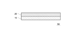
- FIG. 1 is a cross-sectional view schematically showing an example of the structure of the adhesive film for back grinding (adhesive film 50) of this embodiment.
- Adhesive film 50 is used to protect the surface of the wafer.
- the adhesive film 50 includes a substrate layer 10 and an ultraviolet-curable adhesive resin layer 20 (made of an ultraviolet-curable adhesive resin material) provided on one side of the substrate layer 10. configured adhesive resin layer).
- a film with a thickness of 0.2 mm is formed using an ultraviolet curable adhesive resin material, and the film is exposed to ultraviolet rays with a dominant wavelength of 365 nm using a high pressure mercury lamp in an environment of 25 ° C. , the irradiation intensity is 100 W/cm 2 , and the UV dose is 1080 mJ/cm 2 for UV curing to obtain a cured film.
- the dynamic viscoelasticity of the cured film is measured at a frequency of 1 Hz and in a tensile mode within a temperature range of -50 to 200°C.
- E' (-15°C) is preferably in the range of 6.0x10⁸ to 3.0x10⁹Pa .
- the film formed using the UV-curable adhesive resin material is in a state of being bonded to, for example, a release film when the UV irradiation is performed in (i) above.
- a release film when the UV irradiation is performed in (i) above.
- An ultraviolet curable adhesive resin material having a thickness of 0.2 mm and having the same composition as the adhesive resin layer 20 is prepared.
- the ultraviolet curable adhesive resin material is sandwiched between silicone release treated surfaces of a colorless transparent polyethylene terephthalate film (separator) on both sides of which silicone release treatment is applied.
- Examples of the colorless and transparent polyethylene terephthalate film (separator) subjected to silicone release treatment include SP-PET T15 and T18 manufactured by Mitsui Chemicals Tohcello, and Purex A31 and A41 manufactured by Toyobo.
- the obtained sample three-layer configuration of separator/adhesive resin layer 20/separator
- UV irradiation at a UV dose of 1080 mJ/cm 2 for UV curing is irradiated with ultraviolet rays having a dominant wavelength of 365 nm using a high-pressure mercury lamp at an irradiation intensity of 100 W/cm 2 in an environment of 25 ° C. , UV irradiation at a UV dose of 1080 mJ/cm 2 for UV curing.
- the value of E′ (100° C.) is preferably in the range of 5.0 ⁇ 10 6 to 2.0 ⁇ 10 7 Pa.
- the value of E′( ⁇ 15° C.)/E′(100° C.) is preferably in the range of 3.0 ⁇ 10 ⁇ 3 to 1.4 ⁇ 10 ⁇ 2 Pa.
- the value of E′ ( ⁇ 15° C.) is more preferably in the range of 6.7 ⁇ 10 7 to 2.0 ⁇ 10 10 , still more preferably 7.0 ⁇ 10 8 to 2.0 ⁇ 10 9 .
- the peeling of the adhesive film after curing is usually performed at room temperature, but the storage elastic modulus at a high temperature of about 100 ° C., and the (storage elastic modulus at a low temperature of about -15 ° C.) and (at a high temperature of about 100 ° C. It is presumed that the ratio E'(100°C)/E'(-15°C) of storage modulus) is closely related to the mode of peeling. More specifically, it is as follows.
- E' 100° C. is a sufficiently high temperature relative to the glass transition temperature of the adhesive, and the non-crystalline adhesive is considered to be in a completely amorphous state. Therefore, E' (100°C) is considered to indicate the crosslink density of the adhesive. If E′ (100° C.) is too high, the cross-linking density of the adhesive is too high, and toughness is remarkably impaired, and the adhesive is brittle and easily broken. In addition, when E' (100 ° C.) is too low, it means that the cross-linking density is too low, and the interaction between the adhesive material and the adherend is too large and it is difficult to peel off, so adhesive residue is likely to occur. It is estimated to be.
- E' (100 ° C.) / E' (-15 ° C.) is too low, E' (-15 ° C.) is relatively high, and the adhesive material is too hard and brittle during actual peeling. It is presumed that it is easy to break and adhesive residue is likely to occur. Also, if E'(100°C)/E' (-15°C) is too high, E' (-15°C) is relatively small, and the adhesive material is too soft when actually peeled off. It is presumed that the interaction between the material and the adherend is high, making it difficult to peel off and leaving an adhesive residue.
- E' (100 ° C.) is a moderate value corresponds to the fact that the adhesive material has a moderate cross-linking density that makes it difficult for adhesive to remain
- E' (100 ° C.) / E' (-15 °C) is an appropriate value, it can be said that the crosslink density and toughness of the pressure-sensitive adhesive are appropriate. It is presumed that these contribute to the reduction of adhesive residue.
- E' (-15°C) is also estimated.
- the elastic modulus at ⁇ 15° C. It is known that frequency change is very similar to temperature change, and increasing frequency and decreasing temperature show similar effects (time-temperature conversion rule). It is known that the adhesive material undergoes a large instantaneous deformation during tape peeling, and the viscoelastic behavior in the higher frequency range (i.e., the lower temperature range) is thought to be close to the actual peeling mode. . Therefore, tape peeling is usually performed at room temperature, but it is presumed that the storage elastic modulus E' at a lower temperature of -15 ° C. well represents the behavior of the adhesive material when the tape is actually peeled. be done. Therefore, it is presumed that the adhesive residue can be further suppressed by designing the adhesive material so that E' (-15°C) has an appropriate value.
- the adhesive film 50 that satisfies the above regulation of storage elastic modulus can be manufactured by appropriately selecting materials, appropriate blending of each material, manufacturing conditions, and the like. Details of these will be discussed from time to time below.
- Each layer constituting the adhesive film 50 will be specifically described below.
- the base material layer 10 is a layer provided for the purpose of improving properties such as handleability, mechanical properties, and heat resistance of the adhesive film 50 .
- the base material layer 10 is not particularly limited as long as it has a mechanical strength capable of withstanding the external force applied when processing the wafer, and examples thereof include a resin film.
- Examples of the resin constituting the base material layer 10 include polyolefins such as polyethylene, polypropylene, poly(4-methyl-1-pentene) and poly(1-butene); polyester; nylon-6, nylon-66, polyamides such as polymetaxylene adipamide; (meth)acrylic resins such as polyacrylate and polymethacrylate; polyvinyl chloride; polyvinylidene chloride; polyimide; Polyacrylonitrile; polycarbonate; polystyrene; ionomer; polysulfone; polyethersulfone; polyetheretherketone; Among these, from the viewpoint of improving mechanical properties and transparency, one or two selected from the group consisting of polypropylene, polyethylene terephthalate, polyethylene naphthalate, polyamide, polyimide, ethylene-vinyl acetate copolymer and polybutylene terephthalate More than one species is preferable, and one or more selected from polyethylene terephthalate and polyethylene
- the substrate layer 10 may be a single layer or two or more layers.
- the form of the resin film used for providing the base material layer 10 may be a stretched film or a film stretched uniaxially or biaxially. From the viewpoint of improving the mechanical strength of the base material layer 10, the film is preferably uniaxially or biaxially stretched.
- the substrate layer 10 is preferably annealed in advance from the viewpoint of suppressing warpage of the wafer after grinding.
- the substrate layer 10 may be subjected to surface treatment in order to improve adhesion with other layers. Specifically, corona treatment, plasma treatment, undercoat treatment, primer coat treatment, or the like may be performed.
- the thickness of the substrate layer 10 is preferably 20 ⁇ m or more and 250 ⁇ m or less, more preferably 30 ⁇ m or more and 200 ⁇ m or less, and even more preferably 50 ⁇ m or more and 150 ⁇ m or less.
- the adhesive film 50 includes an ultraviolet curable adhesive resin layer 20 .
- the adhesive resin layer 20 is a layer provided on one side of the substrate layer 10, and is a layer that contacts and adheres to the circuit-forming surface of the wafer when the adhesive film 50 is attached to the circuit-forming surface of the wafer. is.
- the adhesive resin layer 20 is formed using an appropriate UV-curable adhesive resin material. Specifically, the adhesive resin layer 20 is formed using an ultraviolet curable adhesive resin material whose adhesive strength is reduced by ultraviolet rays. When the adhesive resin layer 20 is irradiated with ultraviolet rays, it cures (cross-links, etc.) and its adhesive strength is reduced, so that the wafer (or chip obtained by dividing the wafer into pieces) can be easily peeled off from the adhesive film 50 .
- the ultraviolet curable adhesive resin material preferably contains a (meth)acrylic resin known in the fields of pressure sensitive adhesives and adhesives.
- (Meth)acrylic resins include, for example, homopolymers of (meth)acrylic acid ester compounds, copolymers of (meth)acrylic acid ester compounds and comonomers, and the like.
- Examples of (meth)acrylic acid ester compounds that are raw material monomers include methyl (meth)acrylate, ethyl (meth)acrylate, butyl (meth)acrylate, 2-ethylhexyl (meth)acrylate, hydroxyethyl (meth)acrylate, hydroxy Propyl (meth)acrylate, dimethylaminoethyl (meth)acrylate, glycidyl (meth)acrylate and the like. These (meth)acrylic acid ester compounds may be used singly or in combination of two or more.
- Examples of comonomers constituting the (meth)acrylic copolymer include vinyl acetate, (meth)acrylonitrile, styrene, (meth)acrylic acid, itaconic acid, (meth)acrylamide, methylol (meth)acryl amides, maleic anhydride, and the like. When these comonomers are used, they may be used singly or in combination of two or more.
- the UV-curable adhesive resin material preferably contains a (meth)acrylic resin having a polymerizable carbon-carbon double bond at the side chain and/or terminal, and a photoinitiator, and is further crosslinked as necessary. Including drugs, etc.
- the UV-curable adhesive resin material may further contain a low-molecular-weight compound (polyfunctional (meth)acrylate compound, etc.) having two or more polymerizable carbon-carbon double bonds in one molecule.
- a (meth)acrylic resin having a polymerizable carbon-carbon double bond in a side chain and/or terminal is specifically obtained as follows. First, a monomer having an ethylenic double bond and a copolymerizable monomer having a functional group (P) are copolymerized. Next, a functional group (P) contained in this copolymer and a monomer having a functional group (Q) capable of undergoing addition reaction, condensation reaction, etc. with the functional group (P) are combined with each other, leaving the double bond in the monomer A polymerizable carbon-carbon double bond is introduced into the copolymer molecule by reacting in situ.
- Examples of monomers having an ethylenic double bond include alkyl acrylates such as methyl (meth)acrylate, 2-ethylhexyl (meth)acrylate, butyl (meth)acrylate, and ethyl (meth)acrylate, and One or two or more of methacrylic acid alkyl ester monomers, vinyl esters such as vinyl acetate, (meth)acrylonitrile, (meth)acrylamide, and monomers having an ethylenic double bond such as styrene are used.
- alkyl acrylates such as methyl (meth)acrylate, 2-ethylhexyl (meth)acrylate, butyl (meth)acrylate, and ethyl (meth)acrylate
- methacrylic acid alkyl ester monomers vinyl esters such as vinyl acetate, (meth)acrylonitrile, (meth)acrylamide
- monomers having an ethylenic double bond such as
- copolymerizable monomers having a functional group (P) examples include (meth)acrylic acid, maleic acid, 2-hydroxyethyl (meth)acrylate, glycidyl (meth)acrylate, N-methylol (meth)acrylamide, (meth) acryloyloxyethyl isocyanate and the like. These may be used alone or in combination of two or more.
- the ratio of the monomer having an ethylenic double bond and the copolymerizable monomer having a functional group (P) is 70 to 99% by mass of the monomer having an ethylenic double bond, and the copolymer having a functional group (P) preferably 1 to 30% by mass of the reactive monomer.
- the monomer having an ethylenic double bond accounts for 80 to 95% by mass
- the copolymerizable monomer having a functional group (P) accounts for 5 to 20% by mass.
- the monomer having the functional group (Q) include monomers similar to the copolymerizable monomer having the functional group (P).
- a combination such as a carboxyl group and an epoxy group, a carboxyl group and an aziridinyl group, a hydroxyl group and an isocyanate group, etc., in which an addition reaction easily occurs is desirable.
- any reaction such as a condensation reaction between a carboxylic acid group and a hydroxyl group can be applied as long as the reaction can easily introduce a polymerizable carbon-carbon double bond.
- a polymerization initiator can be used when copolymerizing a monomer having an ethylenic double bond and a copolymerizable monomer having a functional group (P).
- examples of polymerization initiators include radical polymerization initiators such as benzoyl peroxide-based polymerization initiators and t-butylperoxy-2-ethylhexanoate.
- Low molecular weight compounds having two or more polymerizable carbon-carbon double bonds in one molecule include, for example, tripropylene glycol di(meth)acrylate, trimethylolpropane tri(meth)acrylate, tetramethylolmethane tetraacrylate, penta Polyfunctional (meth)acrylate compounds such as erythritol tetra(meth)acrylate, dipentaerythritol monohydroxypenta(meth)acrylate, dipentaerythritol penta(meth)acrylate, dipentaerythritol hexa(meth)acrylate, ditrimethylolpropane tetraacrylate, etc. etc.
- the amount of the low molecular weight compound having two or more polymerizable carbon-carbon double bonds in the molecule is preferably 0.1 to 20 parts by mass with respect to 100 parts by mass of the (meth)acrylic resin, More preferably, it is 5 to 18 parts by mass. In addition, the amount of the low-molecular-weight compound having two or more polymerizable carbon-carbon double bonds in the molecule is preferably 0.1 parts by mass or more, with respect to 100 parts by mass of the (meth)acrylic resin.
- a photoinitiator usually generates chemical species (such as radicals) that polymerize polymerizable carbon-carbon double bonds when irradiated with ultraviolet rays.
- photoinitiators include benzoin, isopropylbenzoin ether, isobutylbenzoin ether, benzophenone, Michler ketone, chlorothioxanthone, dodecylthioxanthone, dimethylthioxanthone, diethylthioxanthone, acetophenone diethyl ketal, benzyl dimethyl ketal, 1-hydroxycyclohexylphenyl ketone, 2 -hydroxy-2-methyl-1-phenylpropan-1-one, 2-benzyl-2-dimethylamino-4'-morpholinobutyrophenone, 2,2-dimethoxy-2-phenylacetophenone, 2-dimethylamino-2- (4-methylbenzyl)-1-(4-morpholin-4-yl-phenyl
- a photoinitiator may use only 1 type and may use 2 or more types.
- the amount of the photoinitiator added is preferably 0.1 to 15 parts by mass, more preferably 1 to 10 parts by mass, and still more preferably 4 to 100 parts by mass of the (meth)acrylic resin. 10 parts by mass.
- the amount of the photoinitiator added is preferably 0.1 parts by mass or more, more preferably 1 part by mass or more, still more preferably 3 parts by mass or more, and further preferably 100 parts by mass of the (meth)acrylic resin.
- It is preferably 4 parts by mass or more, more preferably 5 parts by mass or more, and is preferably 15 parts by mass or less, more preferably 12 parts by mass or less, still more preferably 10 parts by mass or less, further preferably 8 parts by mass or less. be.
- the ultraviolet curable adhesive resin material may contain a cross-linking agent.
- cross-linking agents include epoxy compounds such as sorbitol polyglycidyl ether, polyglycerol polyglycidyl ether, pentaerythritol polyglycidyl ether, diglycerol polyglycidyl ether, tetramethylolmethane-tri- ⁇ -aziridinylpropionate, trimethylolpropane-tri- ⁇ -aziridinylpropionate, N,N'-diphenylmethane-4,4'-bis(1-aziridinecarboxamide), N,N'-hexamethylene-1,6-bis( 1-aziridine carboxamide), isocyanate compounds such as tetramethylene diisocyanate, hexamethylene diisocyanate and polyisocyanate. Only one type of cross-linking agent may be used, or two or more types may be used.
- the amount of the cross-linking agent in the UV-curable adhesive resin material is 100 mass of (meth)acrylic resin from the viewpoint of improving the balance between the heat resistance and adhesion of the adhesive resin layer 20. It is preferably 0.1 to 15 parts by mass, more preferably 0.5 to 5 parts by mass.
- the content of the cross-linking agent in the ultraviolet-curable adhesive resin material is, from the viewpoint of improving the balance between the heat resistance and adhesion of the adhesive resin layer 20, the (meth)acrylic resin With respect to 100 parts by mass, preferably 0.1 parts by mass or more, more preferably 0.2 parts by mass or more, still more preferably 0.5 parts by mass or more, still more preferably 0.7 parts by mass or more, and preferably is 15 parts by mass or less, more preferably 10 parts by mass or less, even more preferably 5 parts by mass or less, and even more preferably 3 parts by mass or less.
- the adhesive resin layer 20 can be formed, for example, by applying an ultraviolet curable adhesive resin material on one surface of the base material layer 10 . That is, an ultraviolet curable adhesive resin material prepared by dissolving or dispersing each of the above components in an appropriate solvent (typically an organic solvent) is coated on one surface of the base material layer 10 to form an adhesive layer.
- a flexible resin layer 20 may be provided.
- the coating method conventionally known coating methods such as roll coater method, reverse roll coater method, gravure roll method, bar coater method, comma coater method and die coater method can be employed.
- the drying conditions are not particularly limited, it is generally preferable to dry in a temperature range of 80 to 200° C. for 10 seconds to 10 minutes.
- the pressure-sensitive adhesive coating solution may be heated at 40-80° C. for about 5-300 hours after drying.
- the UV-curable adhesive resin material is applied to the surface of an easily peelable base material (separator) to form an adhesive resin layer 20, and (ii) thereafter, the formed adhesive resin layer is attached to one surface of the base material layer 10.
- the UV-curable adhesive resin material is applied to the surface of an easily peelable base material (separator) to form an adhesive resin layer 20
- the formed adhesive resin layer is attached to one surface of the base material layer 10.
- a method can also be mentioned.
- the thickness of the adhesive resin layer 20 is preferably 5 ⁇ m or more and 300 ⁇ m or less, more preferably 10 ⁇ m or more and 100 ⁇ m or less, and still more preferably 10 ⁇ m or more and 50 ⁇ m or less.
- the thickness of the adhesive resin layer 20 is preferably 5 ⁇ m or more, more preferably 10 ⁇ m or more, still more preferably 20 ⁇ m or more, and preferably 300 ⁇ m or less, more preferably 100 ⁇ m or less, and still more preferably 50 ⁇ m or less.
- Sufficient adhesiveness can be obtained by appropriately increasing the thickness of the adhesive resin layer 20 .
- the adhesive resin layer 20 is not too thick, the handleability of the adhesive film 50 is improved.
- the adhesive film 50 may include other layers as long as the effect of suppressing adhesive residue is not impaired.
- there may be another layer such as an uneven absorbent resin layer, an adhesive layer, or an antistatic layer between each layer.
- an uneven absorbent resin layer By providing the unevenness-absorbing resin layer, the ability of the adhesive film 50 to absorb unevenness can be improved.
- the adhesive layer By providing the adhesive layer, the adhesion between each layer can be improved.
- the antistatic property of the adhesive film 50 can be improved by providing an antistatic layer.
- the exposed surface of the adhesive resin layer 20 may be protected with an appropriate protective film (easy peeling film) such as a release film.
- the thickness of the entire adhesive film 50 is preferably 50 ⁇ m or more and 600 ⁇ m or less, more preferably 50 ⁇ m or more and 400 ⁇ m or less, and still more preferably 50 ⁇ m or more and 300 ⁇ m or less, from the balance of mechanical properties and handleability.
- the adhesive resin layer 20 is formed using an ultraviolet curable adhesive resin material whose adhesive strength is reduced by ultraviolet rays.
- the extent to which the adhesive strength is reduced by ultraviolet rays is preferably quantified as follows.
- F1/F0 is preferably 0.01 to 0.60, more preferably 0.01 to 0.20, and still more preferably 0.02 to 0.20.
- F1/F0 is preferably 0.01 or more, more preferably 0.015 or more, more preferably 0.02 or more, and preferably 0.60 or less, more preferably 0.30 or less, and further It is preferably 0.20 or less, more preferably 0.15 or less, further preferably 0.12 or less.
- F1/F0 By setting F1/F0 to an appropriate value, displacement of the wafer during the backgrinding process can be suppressed, and the adhesive film 50 can be easily peeled off after the backgrinding process.
- the value of F0 itself is, for example, 3 to 20N/25mm, specifically 3 to 16N/25mm.
- the value of F1 itself is, for example, 10 N/25 mm or less, specifically 1 N/25 mm or less, more specifically 0.5 N/25 mm or less.
- F1 may be zero, F1 is generally 0.005 N/25 mm or more, specifically 0.01 N/25 mm or more.
- FIG. 2 is a cross-sectional view schematically showing an example of a method for manufacturing an electronic device using the adhesive film 50.
- a method of manufacturing an electronic device includes, for example, at least the following three steps.
- the electronic device manufacturing method of the present embodiment is characterized in that the adhesive film 50 is used as a so-called back grind tape when grinding the back surface of the wafer 30 .
- Each step of the method for manufacturing an electronic device will be described below.
- Step (A) First, a structure 100 including a wafer 30 having a circuit forming surface 30A and an adhesive film 50 bonded to the circuit forming surface 30A side of the wafer 30 is prepared.
- a structure 100 is produced, for example, by peeling off the release film from the adhesive resin layer 20 of the adhesive film 50 to expose the surface of the adhesive resin layer 20, and then placing the wafer 30 on the adhesive resin layer 20. can be produced by adhering the circuit forming surface 30A.
- the conditions for attaching the circuit forming surface 30A of the wafer 30 to the adhesive film 50 are not particularly limited. It can be 0.5 to 20 mm/sec.
- the step (A) includes at least one selected from a step (A1-1) of half-cutting the wafer 30 and a step (A1-2) of irradiating the wafer 30 with a laser to form a modified layer on the wafer 30. and a step (A2) of attaching the adhesive film 50 for back grinding to the circuit forming surface 30A side of the wafer 30 after the step (A1).
- the adhesive film 50 according to the present embodiment can be suitably used in an electronic device manufacturing process using a pre-dicing method, a pre-stealth method, or the like. Therefore, a manufacturing method in which the above step (A1-1) as a pre-dicing method or the above step (A1-2) as a pre-stealth method is performed is preferable.
- step (A2) the adhesive film 50 can be heated and attached to the circuit forming surface 30A of the wafer 30.
- the heating temperature is not particularly limited, it is, for example, 60 to 80.degree.
- the operation of attaching the adhesive film 50 to the wafer 30 may be performed manually, but in general, it can be performed by a device called an automatic attaching machine equipped with a roll-shaped adhesive film.
- the wafer 30 to be attached to the adhesive film 50 is not particularly limited, but the wafer 30 having the circuit forming surface 30A is preferable.
- Examples include semiconductor wafers, epoxy mold wafers, epoxy mold panels, etc., preferably semiconductor wafers and epoxy mold wafers.
- semiconductor wafers include silicon wafers, sapphire wafers, germanium wafers, germanium-arsenic wafers, gallium-phosphorus wafers, gallium-arsenic-aluminum wafers, gallium-arsenic wafers, lithium tantalate wafers, and silicon wafers.
- Epoxy mold wafers include wafers manufactured by an eWLB (Embedded Wafer Level Ball Grid Array) process, which is one of the methods for manufacturing fan-out WLPs.
- the semiconductor wafer and epoxy mold wafer having a circuit forming surface are not particularly limited, and examples thereof include those on which circuits such as wiring, capacitors, diodes or transistors are formed. Also, the circuit forming surface may be plasma-treated.
- the circuit formation surface 30A of the wafer 30 may be an uneven surface by having, for example, bump electrodes or the like.
- the bump electrode is joined to an electrode formed on the mounting surface to provide an electrical connection between the electronic device and the mounting surface (a mounting surface such as a printed circuit board). It forms a connection.
- Examples of bump electrodes include ball bumps, printed bumps, stud bumps, plated bumps, pillar bumps, and the like. That is, the bump electrodes are usually convex electrodes. These bump electrodes may be used singly or in combination of two or more.
- the height and diameter of the bump electrode are not particularly limited, they are preferably 10 to 400 ⁇ m, more preferably 50 to 300 ⁇ m, respectively.
- the bump pitch at that time is not particularly limited, it is preferably 20 to 600 ⁇ m, more preferably 100 to 500 ⁇ m.
- the type of metal forming the bump electrode is not particularly limited, and examples thereof include solder, silver, gold, copper, tin, lead, bismuth, and alloys thereof. It is preferably used for These metal species may be used singly or in combination of two or more.
- Step (B) the surface of the wafer 30 opposite to the circuit forming surface 30A (also referred to as the back surface) is back ground.
- “Backgrinding” means thinning the wafer 30 to a predetermined thickness without damaging it.
- the structure 100 is fixed to a chuck table or the like of a grinding machine, and the back surface (circuit non-formed surface) of the wafer 30 is ground.
- the wafer 30 is ground until the thickness is less than or equal to the desired thickness.
- the thickness of the wafer 30 before grinding is appropriately determined according to the diameter and type of the wafer 30, and the thickness of the wafer 30 after grinding is determined appropriately according to the size of chips to be obtained, the type of circuit, and the like. Further, when the wafer 30 is half-cut or a modified layer is formed by laser irradiation, the wafer 30 is singulated into chips 31 by the step (B) as shown in FIG. .
- the back surface grinding method is not particularly limited, and a known grinding method can be adopted. Grinding can be performed while cooling the wafer 30 and the whetstone with water. If necessary, a dry polishing process, which is a grinding method that does not use grinding water, can be performed at the end of the grinding process. After finishing the back surface grinding, chemical etching is performed as necessary. Chemical etching is performed by using an etchant selected from the group consisting of an acidic aqueous solution consisting of hydrofluoric acid, nitric acid, sulfuric acid, acetic acid, etc. alone or a mixed solution, an alkaline aqueous solution such as a potassium hydroxide aqueous solution, a sodium hydroxide aqueous solution, etc.
- an etchant selected from the group consisting of an acidic aqueous solution consisting of hydrofluoric acid, nitric acid, sulfuric acid, acetic acid, etc. alone or a mixed solution, an alkaline aqueous solution such as
- the wafer 30 is immersed with the adhesive film 50 adhered thereon. Etching is performed for the purpose of removing strain generated on the back surface of the wafer 30, further thinning the wafer 30, removing oxide films and the like, pretreatment when electrodes are formed on the back surface, and the like.
- the etchant is appropriately selected according to the above purposes.
- Step (C) Next, the adhesive film 50 is removed from the wafer 30 after the adhesive film 50 is irradiated with ultraviolet rays.
- the adhesive film 50 is irradiated with ultraviolet rays at a dose of, for example, 200 mJ/cm 2 or more and 2000 mJ/cm 2 or less, thereby curing the adhesive resin layer 20 with ultraviolet rays and forming the adhesive resin layer 20. and then remove the adhesive film 50 from the wafer 30 .
- Ultraviolet irradiation can be performed using, for example, ultraviolet rays with a dominant wavelength of 365 nm using a high-pressure mercury lamp.
- the irradiation intensity of ultraviolet rays is, for example, 50 mW/cm 2 or more and 500 mW/cm 2 or less.
- wafer 30 Before removing the adhesive film from wafer 30, wafer 30 may be mounted on a dicing tape or a dicing tape with a die attach film.
- the operation of removing the adhesive film 50 from the wafer 30 may be performed manually, but generally can be performed by a device called an automatic peeler.
- the surface of the wafer 30 after peeling off the adhesive film 50 may be cleaned if necessary.
- the cleaning method include wet cleaning such as water cleaning and solvent cleaning, and dry cleaning such as plasma cleaning. In the case of wet cleaning, ultrasonic cleaning may be used together.
- the cleaning method can be appropriately selected depending on the contamination status of the surface of the wafer 30 .
- a step of mounting the obtained chip 31 on a circuit board may be further performed. These steps can be performed based on publicly known information.
- Base material layer 1 polyethylene terephthalate film (manufactured by Toyobo Co., Ltd., product name: E7180, thickness: 50 ⁇ m, single-sided corona-treated product)
- Base layer 2 Laminated film (total thickness: 110 ⁇ m) composed of low-density polyethylene film/polyethylene terephthalate film/low-density polyethylene film produced as follows. It was obtained by laminating a low-density polyethylene film (density: 0.925 kg/m 3 , thickness: 30 ⁇ m) on both sides of a polyethylene terephthalate film (manufactured by Toray Industries, product name: Lumirror S10, thickness: 50 ⁇ m). One side of the obtained laminated film was subjected to corona treatment.
- Base layer 3 Laminated film (total thickness: 145 ⁇ m) composed of polyethylene terephthalate film/ethylene-vinyl acetate copolymer film/acrylic film produced as follows. Polyethylene terephthalate film (manufactured by Toyobo, product name: E7180, thickness: 50 ⁇ m) and ethylene-vinyl acetate copolymer (manufactured by Mitsui-Dow Polychemicals, MFR: 2.5 g/10 min) film (thickness: 70 ⁇ m) was laminated by performing corona treatment on the side of the ethylene/vinyl acetate copolymer film to be bonded to the polyethylene terephthalate film.
- Polyethylene terephthalate film manufactured by Toyobo, product name: E7180, thickness: 50 ⁇ m
- ethylene-vinyl acetate copolymer manufactured by Mitsui-Dow Polychemicals, MFR: 2.5 g/10 min
- the side of the ethylene-vinyl acetate copolymer film opposite to the polyethylene terephthalate film was also subjected to corona discharge treatment.
- the release surface of the release-treated polyethylene terephthalate film (separator) is coated with the acrylic resin coating solution for the base material layer shown below so as to have a dry thickness of 20 ⁇ m and dried.
- a laminated film composed of film/ethylene-vinyl acetate copolymer film was laminated with the ethylene-vinyl acetate copolymer film interposed therebetween, and aged (40° C., 3 days). After that, the separator was peeled off.
- a substrate layer 3 was obtained as described above.
- (Meth)acrylic resin solution) (Meth) acrylic resin solution 1: 49 parts by mass of ethyl acrylate, 20 parts by mass of 2-ethylhexyl acrylate, 21 parts by mass of methyl acrylate, 10 parts by mass of glycidyl methacrylate, and 0.5 parts by mass of a benzoyl peroxide polymerization initiator as a polymerization initiator (solid in terms of minutes) was reacted in a mixed solvent of 65 parts by mass of toluene and 50 parts by mass of ethyl acetate at 80° C. for 10 hours.
- (Meth) acrylic resin solution 2 77 parts by mass of n-butyl acrylate, 16 parts by mass of methyl methacrylate, 16 parts by mass of 2-hydroxyethyl acrylate, and 0.3 parts by mass of t-butyl peroxy-2-ethylhexanoate as a polymerization initiator, The mixture was reacted at 85° C. for 10 hours in a mixed solvent of 20 parts by mass of toluene and 80 parts by mass of ethyl acetate.
- (Meth) acrylic resin solution 3 30 parts by mass of ethyl acrylate, 11 parts by mass of methyl acrylate, 26 parts by mass of 2-ethylhexyl acrylate, 7 parts by mass of 2-hydroxyethyl methacrylate, and 0.8 parts by mass of a benzoyl peroxide polymerization initiator as a polymerization initiator parts (in terms of solid content) were reacted in a mixed solvent of 7 parts by mass of toluene and 50 parts by mass of ethyl acetate at 80° C. for 9 hours. After completion of the reaction, the obtained solution was cooled, and 25 parts by mass of toluene was added to the cooled solution. As described above, a (meth)acrylic resin solution 3 was obtained.
- crosslinking agent Isocyanate-based cross-linking agent (manufactured by Mitsui Chemicals, trade name: Orester P49-75S)
- UV-curable adhesive resin material coating liquid for forming adhesive resin layer
- Each material described in the column of "UV-curable adhesive resin material (coating solution for forming adhesive resin layer)" in Table 1 is uniformly mixed to obtain an ultraviolet-curable adhesive resin material (adhesive resin layer forming). was obtained.
- the ultraviolet curable adhesive resin material (coating liquid for forming an adhesive resin layer) shown in Table 1 was coated with a silicone release-treated polyethylene terephthalate film (separator) (SP-PET T18 manufactured by Mitsui Chemicals Tohcello Co., Ltd. It was applied to a thickness of 31 ⁇ m)). Next, it was dried at 120° C. for 3 minutes to form an adhesive resin layer having a thickness of 30 to 40 ⁇ m.
- a laminate sample having a structure of separator/adhesive resin layer having a thickness of 0.2 mm/separator was obtained.
- the obtained laminate sample was heated in an oven at 40° C. for 3 days for aging.
- the obtained laminate sample (separator/adhesive resin layer/separator structure) was irradiated with ultraviolet rays having a main wavelength of 365 nm using a high-pressure mercury lamp at an intensity of 100 W/cm 2 and an ultraviolet dose of 1080 mJ in an environment of 25 ° C. /cm 2 for UV curing.
- the viscoelasticity was measured using a solid viscoelasticity measuring device (RSA3, manufactured by TA Instruments).
- the cured laminate sample was cut to a width of 10 mm and a length of 50 mm, and the separators on both sides of the cured laminate sample were removed to obtain measurement samples. After that, the measurement sample was set in the apparatus so that the chuck interval was 20 mm. Then, dynamic viscoelasticity was measured in a temperature range of -50 to 200°C at a frequency of 1 Hz and in a tensile mode.
- the UV-curable adhesive resin material (coating solution for forming an adhesive resin layer) shown in Table 1 was applied to a polyethylene terephthalate film (separator) that had been subjected to a silicone release treatment. Then, it was dried at 120° C. for 3 minutes to form an adhesive resin layer having a thickness of 20 ⁇ m.
- the formed adhesive resin layer was attached to the substrate layer to form a laminate. Specifically, when the substrate layer 1 or 2 was used as the substrate layer, it was attached to the corona-treated surface. When the base material layer 3 was used as the base material layer, the separator was peeled off and attached to the acrylic film layer side. The resulting laminate was heated in an oven at 40° C. for 3 days for aging. As described above, an adhesive film for back grinding was obtained.
- Adhesive strength evaluation Measurement of adhesive strength before and after UV irradiation
- i Preparation of adherend wafer for adhesive strength measurement: The mirror surface of a silicon mirror wafer (4-inch single-sided mirror wafer manufactured by SUMCO) was cleaned with ozone using a UV ozone cleaning device (UV-208 manufactured by Technovision) (ozone treatment time: 60 seconds). Thereafter, the mirror surface of the wafer was wiped off with ethanol to obtain an adherend wafer.
- UV ozone cleaning device UV-208 manufactured by Technovision
- Evaluation wafer 1 Using a dicing saw, the mirror surface of a mirror wafer (KST World, 8-inch mirror wafer, diameter: 200 ⁇ 0.5 mm, thickness: 725 ⁇ 50 ⁇ m, single-sided mirror) is half-cut and evaluated. Wafer 1 was obtained. (Blade: ZH05-SD3500-N1-70-DD, chip size: 5 mm ⁇ 8 mm, depth of cut: 58 ⁇ m, blade rotation speed: 30000 rpm). When the evaluation wafer 1 was observed with an optical microscope, the kerf width was 35 ⁇ m.
- Evaluation wafer 2 Using a dicing saw, the mirror surface of a mirror wafer (KST World, 8-inch mirror wafer, diameter: 200 ⁇ 0.5 mm, thickness: 725 ⁇ 50 ⁇ m, single-sided mirror). Cutting was performed (blade: Z09-SD2000-Y1 58 ⁇ 0.25A ⁇ 40 ⁇ 45E-L, chip size: 5 mm ⁇ 8 mm, depth of cut: 15 ⁇ m, blade rotation speed: 30000 rpm). Observation with an optical microscope revealed that the kerf width was 60 ⁇ m.
- a second-stage half-cut is performed (blade: ZH05-SD3500-N1-70-DD, chip size: 5 mm ⁇ 8 mm, cutting depth: 58 ⁇ m, blade rotation speed: 30000 rpm) to obtain evaluation wafer 2. rice field.
- the adhesive film was irradiated with ultraviolet rays having a dominant wavelength of 365 nm at an irradiation intensity of 100 mW/cm 2 using a high-pressure mercury lamp in an environment of 25° C. with an ultraviolet dose of 1080 mJ/cm 2 . .
- the peeling of the adhesive film was performed by the following procedures.
- a separately prepared dicing tape (used as a mounting tape) is applied to the 8-inch wafer ring frame and the above-mentioned individual via the adhesive surface of the dicing tape. It was pasted on the wafer side of the separated wafer.
- a tape peeler HR3000III, manufactured by Nitto Denko
- the adhesive film for pre-dicing evaluation was peeled off from the wafer notch portion with a peeling tape (PET38REL, manufactured by Lasting System). Then, device peelability was evaluated.
- “OK” indicates that the pre-dicing evaluation adhesive film could be peeled off from the wafer at one time.
- E' (100 ° C.) and E' (100 ° C.)/E' (-15 ° C.) are within the appropriate numerical range.
- the generation of adhesive residue after the pre-dicing method was suppressed.
- E' (100 ° C.) and part or all of E' (100 ° C.)/E' (-15 ° C.) are not within the appropriate numerical range.
- adhesive residue occurred after performing the pre-dicing method.
Landscapes
- Chemical & Material Sciences (AREA)
- Organic Chemistry (AREA)
- Chemical Kinetics & Catalysis (AREA)
- Adhesives Or Adhesive Processes (AREA)
- Mechanical Treatment Of Semiconductor (AREA)
- Adhesive Tapes (AREA)
Priority Applications (5)
| Application Number | Priority Date | Filing Date | Title |
|---|---|---|---|
| US18/564,794 US12463080B2 (en) | 2021-05-28 | 2022-05-27 | Back grinding adhesive film and method for manufacturing electronic device |
| JP2023524242A JP7630615B2 (ja) | 2021-05-28 | 2022-05-27 | バックグラインド用粘着性フィルムおよび電子装置の製造方法 |
| KR1020237042337A KR20240005909A (ko) | 2021-05-28 | 2022-05-27 | 백그라인드용 점착성 필름 및 전자 장치의 제조 방법 |
| CN202280038373.0A CN117397007A (zh) | 2021-05-28 | 2022-05-27 | 背面研磨用粘着性膜以及电子装置的制造方法 |
| EP22811398.1A EP4349592A4 (en) | 2021-05-28 | 2022-05-27 | Adhesive film for back sanding and method for producing an electronic device |
Applications Claiming Priority (2)
| Application Number | Priority Date | Filing Date | Title |
|---|---|---|---|
| JP2021090288 | 2021-05-28 | ||
| JP2021-090288 | 2021-05-28 |
Publications (1)
| Publication Number | Publication Date |
|---|---|
| WO2022250130A1 true WO2022250130A1 (ja) | 2022-12-01 |
Family
ID=84228975
Family Applications (1)
| Application Number | Title | Priority Date | Filing Date |
|---|---|---|---|
| PCT/JP2022/021680 Ceased WO2022250130A1 (ja) | 2021-05-28 | 2022-05-27 | バックグラインド用粘着性フィルムおよび電子装置の製造方法 |
Country Status (6)
| Country | Link |
|---|---|
| US (1) | US12463080B2 (https=) |
| EP (1) | EP4349592A4 (https=) |
| JP (1) | JP7630615B2 (https=) |
| KR (1) | KR20240005909A (https=) |
| CN (1) | CN117397007A (https=) |
| WO (1) | WO2022250130A1 (https=) |
Cited By (2)
| Publication number | Priority date | Publication date | Assignee | Title |
|---|---|---|---|---|
| WO2024228364A1 (ja) * | 2023-05-01 | 2024-11-07 | 株式会社レゾナック | 半導体チップの洗浄方法及び半導体装置の製造方法 |
| WO2024228363A1 (ja) * | 2023-05-01 | 2024-11-07 | 株式会社レゾナック | 半導体チップの洗浄方法及び半導体装置の製造方法 |
Families Citing this family (1)
| Publication number | Priority date | Publication date | Assignee | Title |
|---|---|---|---|---|
| KR20260029829A (ko) * | 2024-08-26 | 2026-03-05 | 도레이첨단소재 주식회사 | 리사이클링 이형필름 및 이를 포함하는 소자 |
Citations (7)
| Publication number | Priority date | Publication date | Assignee | Title |
|---|---|---|---|---|
| JP2014075560A (ja) | 2012-10-05 | 2014-04-24 | Lintec Corp | 表面保護シート |
| JP2016072546A (ja) | 2014-10-01 | 2016-05-09 | 古河電気工業株式会社 | 半導体ウエハ表面保護用粘着テープおよび半導体ウエハの加工方法 |
| JP2018195746A (ja) * | 2017-05-19 | 2018-12-06 | 日東電工株式会社 | ダイシングダイボンドフィルム |
| JP2019016633A (ja) * | 2017-07-04 | 2019-01-31 | 日東電工株式会社 | ダイシングテープ、ダイシングダイボンドフィルム、及び半導体装置の製造方法 |
| WO2020246207A1 (ja) * | 2019-06-03 | 2020-12-10 | 三井化学東セロ株式会社 | 電子装置の製造方法 |
| JP2021005623A (ja) * | 2019-06-26 | 2021-01-14 | 日東電工株式会社 | ダイシングテープ、及び、ダイシングダイボンドフィルム |
| JP2021090288A (ja) | 2019-12-04 | 2021-06-10 | 株式会社Soken | 電力変換装置 |
Family Cites Families (7)
| Publication number | Priority date | Publication date | Assignee | Title |
|---|---|---|---|---|
| JP5049620B2 (ja) | 2007-03-20 | 2012-10-17 | リンテック株式会社 | 粘着シート |
| JP2008251934A (ja) * | 2007-03-30 | 2008-10-16 | Lintec Corp | 半導体チップの製造方法 |
| JP4717085B2 (ja) | 2008-01-18 | 2011-07-06 | 日東電工株式会社 | ダイシング・ダイボンドフィルム |
| EP3040389B1 (en) * | 2013-08-30 | 2021-04-21 | LINTEC Corporation | Sheet for processing semiconductor |
| JP6169067B2 (ja) | 2014-12-24 | 2017-07-26 | 古河電気工業株式会社 | 電子部品加工用粘着テープ |
| CN112004899B (zh) | 2018-04-24 | 2023-01-10 | 三井化学东赛璐株式会社 | 粘着性膜及电子装置的制造方法 |
| JP2020098861A (ja) | 2018-12-18 | 2020-06-25 | 日東電工株式会社 | 接着フィルム、ダイシングテープ付き接着フィルム、および半導体装置製造方法 |
-
2022
- 2022-05-27 KR KR1020237042337A patent/KR20240005909A/ko not_active Ceased
- 2022-05-27 WO PCT/JP2022/021680 patent/WO2022250130A1/ja not_active Ceased
- 2022-05-27 EP EP22811398.1A patent/EP4349592A4/en not_active Withdrawn
- 2022-05-27 CN CN202280038373.0A patent/CN117397007A/zh not_active Withdrawn
- 2022-05-27 US US18/564,794 patent/US12463080B2/en active Active
- 2022-05-27 JP JP2023524242A patent/JP7630615B2/ja active Active
Patent Citations (7)
| Publication number | Priority date | Publication date | Assignee | Title |
|---|---|---|---|---|
| JP2014075560A (ja) | 2012-10-05 | 2014-04-24 | Lintec Corp | 表面保護シート |
| JP2016072546A (ja) | 2014-10-01 | 2016-05-09 | 古河電気工業株式会社 | 半導体ウエハ表面保護用粘着テープおよび半導体ウエハの加工方法 |
| JP2018195746A (ja) * | 2017-05-19 | 2018-12-06 | 日東電工株式会社 | ダイシングダイボンドフィルム |
| JP2019016633A (ja) * | 2017-07-04 | 2019-01-31 | 日東電工株式会社 | ダイシングテープ、ダイシングダイボンドフィルム、及び半導体装置の製造方法 |
| WO2020246207A1 (ja) * | 2019-06-03 | 2020-12-10 | 三井化学東セロ株式会社 | 電子装置の製造方法 |
| JP2021005623A (ja) * | 2019-06-26 | 2021-01-14 | 日東電工株式会社 | ダイシングテープ、及び、ダイシングダイボンドフィルム |
| JP2021090288A (ja) | 2019-12-04 | 2021-06-10 | 株式会社Soken | 電力変換装置 |
Non-Patent Citations (1)
| Title |
|---|
| See also references of EP4349592A4 |
Cited By (4)
| Publication number | Priority date | Publication date | Assignee | Title |
|---|---|---|---|---|
| WO2024228364A1 (ja) * | 2023-05-01 | 2024-11-07 | 株式会社レゾナック | 半導体チップの洗浄方法及び半導体装置の製造方法 |
| JPWO2024228364A1 (https=) * | 2023-05-01 | 2024-11-07 | ||
| WO2024228363A1 (ja) * | 2023-05-01 | 2024-11-07 | 株式会社レゾナック | 半導体チップの洗浄方法及び半導体装置の製造方法 |
| JP7794362B2 (ja) | 2023-05-01 | 2026-01-06 | 株式会社レゾナック | 半導体チップの洗浄方法及び半導体装置の製造方法 |
Also Published As
| Publication number | Publication date |
|---|---|
| US20240274460A1 (en) | 2024-08-15 |
| CN117397007A (zh) | 2024-01-12 |
| JP7630615B2 (ja) | 2025-02-17 |
| EP4349592A4 (en) | 2025-05-28 |
| EP4349592A1 (en) | 2024-04-10 |
| JPWO2022250130A1 (https=) | 2022-12-01 |
| US12463080B2 (en) | 2025-11-04 |
| KR20240005909A (ko) | 2024-01-12 |
Similar Documents
| Publication | Publication Date | Title |
|---|---|---|
| JP7630615B2 (ja) | バックグラインド用粘着性フィルムおよび電子装置の製造方法 | |
| JP2026004450A (ja) | 電子装置の製造方法 | |
| JP7781872B2 (ja) | バックグラインド用粘着性フィルムおよび電子装置の製造方法 | |
| JP7630616B2 (ja) | 電子装置の製造方法 | |
| JP7630617B2 (ja) | 電子装置の製造方法 | |
| JP7588228B2 (ja) | バックグラインド用粘着性フィルムおよび電子装置の製造方法 | |
| JP7588226B2 (ja) | 電子装置の製造方法 | |
| JP7588227B2 (ja) | 電子装置の製造方法 | |
| WO2022250129A1 (ja) | 電子装置の製造方法 |
Legal Events
| Date | Code | Title | Description |
|---|---|---|---|
| 121 | Ep: the epo has been informed by wipo that ep was designated in this application |
Ref document number: 22811398 Country of ref document: EP Kind code of ref document: A1 |
|
| WWE | Wipo information: entry into national phase |
Ref document number: 2023524242 Country of ref document: JP |
|
| WWE | Wipo information: entry into national phase |
Ref document number: 202280038373.0 Country of ref document: CN Ref document number: 18564794 Country of ref document: US |
|
| ENP | Entry into the national phase |
Ref document number: 20237042337 Country of ref document: KR Kind code of ref document: A |
|
| WWE | Wipo information: entry into national phase |
Ref document number: 1020237042337 Country of ref document: KR |
|
| NENP | Non-entry into the national phase |
Ref country code: DE |
|
| WWE | Wipo information: entry into national phase |
Ref document number: 2022811398 Country of ref document: EP |
|
| ENP | Entry into the national phase |
Ref document number: 2022811398 Country of ref document: EP Effective date: 20240102 |
|
| WWG | Wipo information: grant in national office |
Ref document number: 18564794 Country of ref document: US |
|
| WWW | Wipo information: withdrawn in national office |
Ref document number: 2022811398 Country of ref document: EP |
|
| WWC | Wipo information: continuation of processing after refusal or withdrawal |
Ref document number: 1020237042337 Country of ref document: KR |