WO2022249556A1 - 増幅回路および電子機器 - Google Patents
増幅回路および電子機器 Download PDFInfo
- Publication number
- WO2022249556A1 WO2022249556A1 PCT/JP2022/004256 JP2022004256W WO2022249556A1 WO 2022249556 A1 WO2022249556 A1 WO 2022249556A1 JP 2022004256 W JP2022004256 W JP 2022004256W WO 2022249556 A1 WO2022249556 A1 WO 2022249556A1
- Authority
- WO
- WIPO (PCT)
- Prior art keywords
- impedance
- circuit
- capacitor
- transistor
- amplifier
- Prior art date
- Legal status (The legal status is an assumption and is not a legal conclusion. Google has not performed a legal analysis and makes no representation as to the accuracy of the status listed.)
- Ceased
Links
Images









Classifications
-
- H—ELECTRICITY
- H03—ELECTRONIC CIRCUITRY
- H03F—AMPLIFIERS
- H03F3/00—Amplifiers with only discharge tubes or only semiconductor devices as amplifying elements
- H03F3/20—Power amplifiers, e.g. Class B amplifiers, Class C amplifiers
- H03F3/24—Power amplifiers, e.g. Class B amplifiers, Class C amplifiers of transmitter output stages
-
- H—ELECTRICITY
- H03—ELECTRONIC CIRCUITRY
- H03F—AMPLIFIERS
- H03F1/00—Details of amplifiers with only discharge tubes, only semiconductor devices or only unspecified devices as amplifying elements
- H03F1/08—Modifications of amplifiers to reduce detrimental influences of internal impedances of amplifying elements
- H03F1/083—Modifications of amplifiers to reduce detrimental influences of internal impedances of amplifying elements in transistor amplifiers
- H03F1/086—Modifications of amplifiers to reduce detrimental influences of internal impedances of amplifying elements in transistor amplifiers with FET's
-
- H—ELECTRICITY
- H03—ELECTRONIC CIRCUITRY
- H03F—AMPLIFIERS
- H03F1/00—Details of amplifiers with only discharge tubes, only semiconductor devices or only unspecified devices as amplifying elements
- H03F1/56—Modifications of input or output impedances, not otherwise provided for
-
- H—ELECTRICITY
- H03—ELECTRONIC CIRCUITRY
- H03F—AMPLIFIERS
- H03F1/00—Details of amplifiers with only discharge tubes, only semiconductor devices or only unspecified devices as amplifying elements
- H03F1/56—Modifications of input or output impedances, not otherwise provided for
- H03F1/565—Modifications of input or output impedances, not otherwise provided for using inductive elements
-
- H—ELECTRICITY
- H03—ELECTRONIC CIRCUITRY
- H03F—AMPLIFIERS
- H03F3/00—Amplifiers with only discharge tubes or only semiconductor devices as amplifying elements
- H03F3/189—High-frequency amplifiers, e.g. radio frequency amplifiers
- H03F3/19—High-frequency amplifiers, e.g. radio frequency amplifiers with semiconductor devices only
- H03F3/193—High-frequency amplifiers, e.g. radio frequency amplifiers with semiconductor devices only with field-effect devices
-
- H—ELECTRICITY
- H03—ELECTRONIC CIRCUITRY
- H03F—AMPLIFIERS
- H03F3/00—Amplifiers with only discharge tubes or only semiconductor devices as amplifying elements
- H03F3/189—High-frequency amplifiers, e.g. radio frequency amplifiers
- H03F3/19—High-frequency amplifiers, e.g. radio frequency amplifiers with semiconductor devices only
- H03F3/195—High-frequency amplifiers, e.g. radio frequency amplifiers with semiconductor devices only in integrated circuits
-
- H—ELECTRICITY
- H03—ELECTRONIC CIRCUITRY
- H03F—AMPLIFIERS
- H03F3/00—Amplifiers with only discharge tubes or only semiconductor devices as amplifying elements
- H03F3/20—Power amplifiers, e.g. Class B amplifiers, Class C amplifiers
- H03F3/24—Power amplifiers, e.g. Class B amplifiers, Class C amplifiers of transmitter output stages
- H03F3/245—Power amplifiers, e.g. Class B amplifiers, Class C amplifiers of transmitter output stages with semiconductor devices only
-
- H—ELECTRICITY
- H03—ELECTRONIC CIRCUITRY
- H03H—IMPEDANCE NETWORKS, e.g. RESONANT CIRCUITS; RESONATORS
- H03H7/00—Multiple-port networks comprising only passive electrical elements as network components
- H03H7/38—Impedance-matching networks
-
- H—ELECTRICITY
- H03—ELECTRONIC CIRCUITRY
- H03F—AMPLIFIERS
- H03F2200/00—Indexing scheme relating to amplifiers
- H03F2200/387—A circuit being added at the output of an amplifier to adapt the output impedance of the amplifier
Definitions
- the present disclosure relates to an amplifier circuit that amplifies a signal, and an electronic device equipped with such an amplifier circuit.
- Patent Document 1 discloses an amplifier circuit having a first-stage transistor, a second-stage transistor, and a capacitor provided between the drain of the first-stage transistor and the source of the second-stage transistor. is disclosed.
- signals having various signal amplitudes can be input to the amplifier circuit.
- the amplifier circuit is desired to be able to amplify the signals regardless of the signal amplitude.
- An amplifier circuit includes an input terminal, an output terminal, one or more transistors, an amplitude detection circuit, and an impedance circuit.
- One or more transistors are provided in a path connecting the input terminal and the output terminal.
- the amplitude detection circuit is configured to detect the signal amplitude of the input signal at the input terminal.
- the impedance circuit can change the impedance, and is configured to be able to set operating conditions for one or more transistors based on the detection result of the amplitude detection circuit.
- An electronic device includes a communication circuit.
- the communication circuit is capable of wireless communication and has an amplifier circuit.
- the amplifier circuit has an input terminal, an output terminal, one or more transistors, an amplitude detection circuit, and an impedance circuit.
- One or more transistors are provided in a path connecting the input terminal and the output terminal.
- the amplitude detection circuit is configured to detect the signal amplitude of the input signal at the input terminal.
- the impedance circuit can change the impedance, and is configured to be able to set operating conditions for one or more transistors based on the detection result of the amplitude detection circuit.
- one or more transistors provided on a path connecting an input terminal and an output terminal perform an amplification operation based on an input signal at the input terminal.
- the signal amplitude of this input signal is detected by the amplitude detection circuit.
- the impedance circuit changes the impedance based on the detection result of the amplitude detection circuit. This sets the operating conditions for one or more transistors.
- FIG. 1 is a circuit diagram showing a configuration example of a power amplifier according to an embodiment of the present disclosure
- FIG. 2 is an explanatory diagram showing power amplification operation in the power amplifier shown in FIG. 1
- FIG. 3 is another explanatory diagram showing the power amplification operation in the power amplifier shown in FIG. 1
- FIG. 2 is a circuit diagram showing a configuration example of an impedance control circuit shown in FIG. 1
- FIG. 2 is another circuit diagram showing a configuration example of the impedance control circuit shown in FIG. 1.
- FIG. 2 is another circuit diagram showing a configuration example of the impedance control circuit shown in FIG. 1.
- FIG. 5 is a timing chart showing an operation example of the amplitude detection circuit shown in FIG. 4;
- FIG. 5 is a timing chart showing an operation example of the amplitude detection circuit shown in FIG. 4;
- FIG. 5 is a timing chart showing an operation example of the amplitude detection circuit shown in FIG. 4; FIG.
- FIG. 2 is a table showing an example of impedance settings in the power amplifier shown in FIG. 1; 2 is a waveform diagram showing an operation example in the power amplifier shown in FIG. 1; FIG. 3 is another waveform diagram showing an operation example of the power amplifier shown in FIG. 1.
- FIG. 3 is another waveform diagram showing an operation example of the power amplifier shown in FIG. 1.
- FIG. 3 is another waveform diagram showing an operation example of the power amplifier shown in FIG. 1.
- FIG. 3 is a waveform diagram showing an operation example with another impedance setting in the power amplifier shown in FIG. 1;
- FIG. 10 is another waveform diagram showing an operation example with another impedance setting in the power amplifier shown in FIG. 1 ;
- FIG. 10 is another waveform diagram showing an operation example with another impedance setting in the power amplifier shown in FIG. 1 ;
- FIG. 10 is another waveform diagram showing an operation example with another impedance setting in the power amplifier shown in FIG. 1 ;
- FIG. 11 is a circuit diagram showing a configuration example of a power amplifier according to a modification;
- FIG. 11 is a circuit diagram showing a configuration example of a power amplifier according to another modified example;
- 1 is a perspective view showing an external configuration of a smartphone to which a power amplifier according to one embodiment is applied;
- FIG. 1 shows a configuration example of a power amplifier (power amplifier 1) according to one embodiment.
- the power amplifier 1 is provided, for example, in a smartphone capable of wireless communication in a fifth generation (5G) mobile communication system.
- the power amplifier 1 includes an input terminal Tin, a matching circuit 11, a bias circuit 12, a resistive element R1, a transistor FET1, an inductor L1, a capacitor C1, an inductor L2, a transistor FET2, a capacitor C2, a resistor An element R2, an inductor L3, a matching circuit 13, an output terminal Tout, and an impedance control circuit 14 are provided.
- the input terminal Tin is configured so that the input signal Sin is supplied from the preceding circuit of the power amplifier 1 .
- the power amplifier 1 generates an output signal Sout by performing a power amplification operation based on this input signal Sin.
- the matching circuit 11 is configured to match the impedance of the input of the transistor FET1.
- Matching circuit 11 includes, for example, one or more capacitors and one or more inductors.
- the matching circuit 11 adjusts the impedance of the matching circuit 11 by changing the impedance of one or more elements of the one or more capacitors and one or more inductors based on the control signal supplied from the impedance control circuit 14 . can be changed.
- the input terminal of the matching circuit 11 is connected to the input terminal Tin of the power amplifier 1, and the output terminal is connected to the resistive element R1 and the gate of the transistor FET1.
- the bias circuit 12 is configured to generate a bias voltage Vg.
- a bias voltage Vg is supplied to one end of the resistance element R1, and the other end is connected to the output terminal of the matching circuit 11 and the gate of the transistor FET1.
- transistor FET1 The gate of transistor FET1 is connected to the output terminal of matching circuit 11 and resistor element R1, the source is grounded, and the drain is connected to capacitor C1 and inductor L1.
- a power supply voltage VDD is supplied to one end of the inductor L1, and the other end is connected to the drain of the transistor FET1 and the capacitor C1.
- the capacitor C ⁇ b>1 is configured to be able to change the impedance based on the control signal supplied from the impedance control circuit 14 .
- the capacitor C1 includes, for example, a plurality of capacitors, as will be described later, and the impedance can be changed by changing the number of capacitors used among the plurality of capacitors.
- One end of capacitor C1 is connected to the source of transistor FET2 and inductor L2, and the other end is connected to the drain of transistor FET1 and inductor L1.
- the inductor L2 is configured to be able to change the impedance based on the control signal supplied from the impedance control circuit 14.
- the inductor L2 includes, for example, a plurality of inductors as described later, and the impedance can be changed by changing the number of inductors used among the plurality of inductors.
- One end of inductor L2 is connected to the source of transistor FET2 and capacitor C1, and the other end is grounded.
- the gate of the transistor FET2 is connected to the capacitor C2 and the resistance element R2, the source is grounded to the capacitor C1 and the inductor L2, and the drain is connected to the inductor L3 and the input terminal of the matching circuit 13.
- Capacitor C2 is configured to be able to change the impedance based on the control signal supplied from the impedance control circuit 14.
- Capacitor C2 includes, for example, a varactor as described later, and the impedance can be changed by changing the bias voltage of the varactor.
- One end of capacitor C2 is connected to the gate of transistor FET2 and resistance element R2, and the other end is grounded.
- a bias voltage Vg is supplied to one end of the resistance element R2, and the other end is connected to the capacitor C2 and the gate of the transistor FET2.
- a power supply voltage VDD is supplied to one end of the inductor L3, and the other end is connected to the drain of the transistor FET2 and the input terminal of the matching circuit 13.
- the matching circuit 13 is configured to match the impedance of the output of the transistor FET2.
- Matching circuit 13 includes, for example, one or more capacitors and one or more inductors.
- the matching circuit 13 adjusts the impedance of the matching circuit 13 by changing the impedance of one or more elements of the one or more capacitors and one or more inductors based on the control signal supplied from the impedance control circuit 14 . can be changed.
- the input terminal of the matching circuit 13 is connected to the drain of the transistor FET2 and the inductor L3, and the output terminal is connected to the output terminal Tout of the power amplifier 1.
- the output terminal Tout is configured to output the output signal Sout generated by the power amplifier 1 .
- the output terminal Tout is connected to, for example, an antenna (not shown). As a result, the output signal Sout generated by the power amplifier 1 is transmitted from the antenna as a radio signal.
- the power amplifier 1 uses the two transistors FET1 and FET2 to perform power amplification based on the input signal Sin.
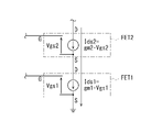
- FIGS. 2 and 3 schematically show the operation of the power amplifier 1 with respect to an AC signal. Since FIGS. 2 and 3 describe the operation with respect to an AC signal, the illustration of the capacitor C1 and the inductors L1 and L2 is omitted for convenience of description.
- the size and characteristics of the transistor FET1 and the size and characteristics of the transistor FET2 are the same as each other.
- the current characteristics of the transistor FET1 and the current characteristic of the transistor FET2 are the same, and the operating point of the transistor FET1 and the operating point of the transistor FET2 are the same.
- the operating point voltage of the gates of the transistors FET1 and FET2 is the bias voltage Vg
- the operating point voltage of the sources is the ground voltage
- the operating point voltage of the drains is the power supply voltage VDD.
- An alternating signal current corresponding to the input signal Sin flows through the transistors FET1 and FET2 as indicated by arrows in FIG.
- the current Ids1 flowing from the drain to the source in the transistor FET1 is expressed as follows using the transconductance gm1 of the transistor FET1 and the voltage Vgs1 between the gate and source of the transistor FET1.
- Ids1 gm1 Vgs1
- the current Ids2 flowing from the drain to the source in the transistor FET2 is expressed as follows using the transconductance gm2 of the transistor FET2 and the voltage Vgs2 between the gate and source of the transistor FET2.
- Ids2 gm2 Vgs2
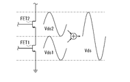
- the power amplifier 1 should transmit power so that the voltages Vgs1 and Vgs2 are equal, the currents Ids1 and Ids2 are equal, and the voltages Vds1 and Vds2 are equal.
- the power amplifier 1 uses the transistor FET2 to amplify the power amplified by the transistor FET1 with a current gain of 1 and a voltage gain of 2. That is, as shown in FIG. 3, the voltage Vds output by the power amplifier 1 is the total voltage of the voltages Vds1 and Vds2.
- the load impedances of transistors FET1 and FET2 are adjusted.
- the impedance control circuit 14 detects the signal amplitude of the input signal Sin based on the input signal Sin, and adjusts the impedances of the matching circuit 11, the capacitor C1, the inductor L2, the capacitor C2, and the matching circuit 13 based on the signal amplitude. It is configured to generate five control signals for each setting.
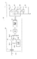
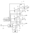
- FIG. 4A shows a configuration example of a circuit portion of the impedance control circuit 14 that controls the impedance of the capacitor C2. Capacitor C2 is also depicted in FIG. 4A.
- the impedance control circuit 14 has an amplitude detection circuit 20, a DAC 31, and a resistance element R32.
- the amplitude detection circuit 20 has a coupler 21, a bias circuit 22, a resistance element R23, a buffer amplifier 24, a diode D25, a capacitor C26, and an ADC (Analog to Digital Converter) 27.
- ADC Analog to Digital Converter
- the coupler 21 is configured to separate the AC signal contained in the input signal Sin supplied to the input terminal Tin and to supply the separated AC signal to the buffer amplifier 24 as the AC signal Sac1.
- the coupler 21 is configured using, for example, a transmission line.
- the bias circuit 22 is configured to generate a bias voltage.
- a bias voltage generated by the bias circuit 22 is supplied to one end of the resistance element R23, and the other end is connected to the input terminal of the buffer amplifier 24.
- the buffer amplifier 24 is configured to generate an AC signal Sac2 corresponding to the AC signal Sac1.
- the input terminal of buffer amplifier 24 is connected to coupler 21 and resistance element R23, and the output terminal is connected to the anode of diode D25.
- the anode of diode D25 is connected to the output terminal of buffer amplifier 24, and the cathode is connected to the input terminals of capacitor C26 and ADC27.
- One end of capacitor C26 is connected to the cathode of diode D25 and the input terminal of ADC27, and the other end is grounded.
- the ADC 27 is configured to generate a digital code by performing AD conversion based on the voltage at the capacitor C26.
- the digital code is, for example, a multi-bit digital code.
- the input terminal of ADC27 is connected to the cathode of diode D25 and capacitor C26, and the output terminal is connected to the input terminal of DAC31.
- DAC 31 is configured to generate a voltage based on the digital code generated by ADC 27 .
- the input terminal of DAC31 is connected to the output terminal of ADC27, and the output terminal is connected to resistance element R32.
- One end of the resistance element R32 is connected to the output terminal of the DAC31, and the other end is connected to the capacitor C2.
- DAC 31 increases the voltage supplied to capacitor C2 based on such a digital code.
- the peak level of the AC signal Sac1 is high.
- the peak level of AC signal Sac2 is also low, so the voltage on capacitor C26 is low.
- the value of the digital code generated by the ADC 27 is small.
- DAC 31 lowers the voltage supplied to capacitor C2 based on such a digital code.
- the voltage supplied to the capacitor C2 is increased when the signal amplitude of the input signal Sin is large, and the voltage supplied to the capacitor C2 is decreased when the signal amplitude of the input signal Sin is small.
- a logic circuit that converts digital codes may be provided between the ADC 27 and the DAC 31 .
- the capacitor C2 has a varactor 91 and a capacitor 92 in this example.
- the varactor 91 is configured such that the capacitance value can be changed according to the voltage difference between both ends.
- the anode of varactor 91 is grounded and the cathode is connected to resistor R32 and capacitor 92 .
- One end of capacitor C2 is connected to resistor R32 and the cathode of varactor 91, and the other end is connected to the gate of transistor FET2 and resistor R2 as shown in FIG.
- Varactor 91 and capacitor 92 are connected in series with each other.
- the capacitance of capacitor C2 is the combined capacitance of varactor 91 and capacitor 92 connected in series.
- FIG. 4B shows a configuration example of a circuit portion of the impedance control circuit 14 that controls the impedance of the capacitor C1.
- the impedance control circuit 14 has a control circuit 33 .
- Capacitor C1 is also depicted in FIG. 4B.
- the control circuit 33 is configured to generate three control signals for switching the impedance of the capacitor C1 based on the digital code generated by the ADC27.
- the capacitor C1 has capacitors 71-74 and switches 75-77.
- Capacitor 71 has one end connected to capacitors 72-74 and to the source of transistor FET2 and inductor L2 as shown in FIG. 1, and the other end connected to switches 75-77 and shown in FIG. It is connected to the drain of transistor FET1 and inductor L1 as before.
- Capacitor 72 has one end connected to capacitors 71, 73 and 74, as well as the source of transistor FET2 and inductor L2 as shown in FIG.
- One end of capacitor 73 is connected to capacitors 71, 72 and 74, as well as to the source of transistor FET2 and inductor L2 as shown in FIG.
- a capacitor 74 has one end connected to the capacitors 71 to 73 and also to the source of the transistor FET2 and the inductor L2 as shown in FIG.
- the switch 75 is configured to be connected to the other end of the capacitor 72 and the other end of the capacitor 71 by turning on based on the control signal supplied from the control circuit 33 .
- the switch 76 is configured to ground the other end of the capacitor 73 and the other end of the capacitor 71 by turning on based on the control signal supplied from the control circuit 33 .
- the switch 77 is configured to connect the other end of the capacitor 74 and the other end of the capacitor 71 by turning on based on the control signal supplied from the control circuit 33 .
- Capacitor 71 is always valid.
- the capacitance of capacitor C1 is the sum of the capacitances of the effective ones of capacitors 71-74. In this manner, the impedance of the capacitor C1 can be changed by changing the number of the capacitors 71 to 74 that are enabled.
- FIG. 5 shows a configuration example of a circuit portion that controls the impedance of the inductor L2 in the impedance control circuit 14.
- the impedance control circuit 14 has a control circuit 34 .
- inductor L2 is also depicted.
- the control circuit 34 is configured to generate three control signals for switching the impedance of the inductor L2 based on the digital code generated by the ADC27.
- the inductor L2 has inductors 81-84 and switches 85-87.
- One end of inductor 81 is connected to the source of transistor FET2 and capacitor C1 as shown in FIG.
- One end of inductor 82 is connected to the other end of inductor 81 and the other end is connected to one end of inductor 83 .
- One end of inductor 83 is connected to the other end of inductor 82 and the other end is connected to one end of inductor 84 .
- One end of inductor 84 is connected to the other end of inductor 83, and the other end is grounded.
- the switch 85 is configured to ground the other end of the inductor 81 and one end of the inductor 82 by turning on based on the control signal supplied from the control circuit 34 .
- the switch 86 is configured to ground the other end of the inductor 82 and one end of the inductor 83 by turning on based on the control signal supplied from the control circuit 34 .
- the switch 87 is configured to ground the other end of the inductor 83 and one end of the inductor 84 by turning on based on the control signal supplied from the control circuit 34 .
- the inductance of inductor L2 is equal to the inductance of inductor 81 .
- the inductance of inductor L2 is the total inductance of the inductances of inductors 81 and 82 .
- the switches 85 and 86 are off and the switch 87 is on, the inductors 81 to 83 are enabled and the inductor 84 is disabled.
- the inductance of inductor L2 is the sum of the inductances of inductors 81-83. Also, for example, when the switches 85-87 are in the off state, the inductors 81-84 are enabled. Therefore, the inductance of inductor L2 is the sum of the inductances of inductors 81-84. In this manner, the impedance of the inductor L2 can be changed by changing the number of inductors 81 to 84 that are enabled.
- FIG. 4A describes the circuit portion that controls the impedance of the capacitor C2
- FIG. 4B describes the circuit portion that controls the impedance of the capacitor C1
- FIG. 5 describes the circuit portion that controls the impedance of the inductor L2.
- matching circuit 11 includes, for example, one or more capacitors and one or more inductors, and changing the impedance of one or more of these elements changes the impedance of matching circuit 11. can be done. Therefore, by applying the configurations shown in FIGS. 4A, 4B, and 5 to these elements, the impedance of the matching circuit 11 can be controlled. The same applies to the matching circuit 13 as well.
- the impedances of the matching circuit 11, the capacitor C1, the inductor L2, the capacitor C2, and the matching circuit 13 can be set according to the signal amplitude of the input signal Sin.
- the operating conditions of the transistors FET1 and FET2 are set by setting the impedances of the matching circuit 11, the capacitor C1, the inductor L2, the capacitor C2, and the matching circuit 13.
- the input terminal Tin corresponds to a specific example of "input terminal” in the present disclosure.
- the output terminal Tout corresponds to a specific example of "output terminal” in the present disclosure.
- the transistors FET1 and FET2 correspond to a specific example of “one or more transistors” in the present disclosure.
- the transistor FET1 corresponds to a specific example of "first transistor” in the present disclosure.
- the transistor FET2 corresponds to a specific example of "second transistor” in the present disclosure.
- the amplitude detection circuit 20 corresponds to a specific example of "amplitude detection circuit” in the present disclosure.
- the matching circuit 11, the capacitor C1, the inductor L2, the capacitor C2, and the matching circuit 13 correspond to a specific example of "impedance circuit” in the present disclosure.
- Coupler 21 corresponds to a specific example of the "isolation element" in this disclosure.
- the buffer amplifier 24 corresponds to a specific example of “buffer amplifier” in the present disclosure.
- Diode D25 corresponds to a specific example of “diode” in the present disclosure.
- Capacitor C26 corresponds to a specific example of the "first capacitor” in the present disclosure.
- the power amplifier 1 generates an output signal Sout by performing a power amplification operation based on the input signal Sin.
- the impedance control circuit 14 detects the signal amplitude of the input signal Sin based on the input signal Sin, and adjusts the impedances of the matching circuit 11, the capacitor C1, the inductor L2, the capacitor C2, and the matching circuit 13 based on the signal amplitude. Generate five control signals for each setting.
- the matching circuit 11 changes impedance based on the control signal supplied from the impedance control circuit 14 .
- Capacitor C1 changes impedance based on a control signal supplied from impedance control circuit 14 .
- Inductor L2 changes impedance based on a control signal supplied from impedance control circuit 14 .
- Capacitor C2 changes impedance based on the control signal supplied from impedance control circuit 14 .
- the matching circuit 13 changes impedance based on the control signal supplied from the impedance control circuit 14 .
- the power amplifier 1 changes the impedances of the matching circuit 11, the capacitor C1, the inductor L2, the capacitor C2, and the matching circuit 13 based on the signal amplitude of the input signal Sin.
- An operation of changing the impedance of the capacitor C2 will be described below as an example with reference to FIG.
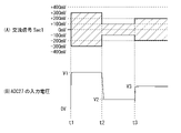
- FIG. 6 shows an operation example of the amplitude detection circuit 20 in the impedance control circuit 14, where (A) shows the envelope of the AC signal Sac1 and (B) shows the input voltage of the ADC27.
- the signal amplitude of the input signal Sin becomes 600 mVpp.
- Coupler 21 separates the AC signal contained in input signal Sin.
- the separated AC signal Sac1 has a peak level of "+300 mV” and a bottom level of "-300 mV”.
- the buffer amplifier 24 generates an AC signal Sac2 corresponding to the AC signal Sac1, and the diode D25 and the capacitor C26 perform peak hold operation.
- the input voltage of the ADC 27 becomes a voltage (voltage V1) corresponding to the peak level of the AC signal Sac1, as shown in FIG. 6(B).
- the ADC 27 performs AD conversion based on this input voltage to generate a digital code, and the DAC 31 generates a voltage based on the digital code generated by the ADC 27 .
- the cathode voltage of the varactor 91 becomes a voltage corresponding to the voltage V1.
- the capacitance of capacitor C2, which includes varactor 91 is the capacitance corresponding to this cathode voltage.
- the signal amplitude of the input signal Sin changes from 600 mVpp to 200 mVpp.
- the separated AC signal Sac1 has a peak level of "+100 mV” and a bottom level of "-100 mV”.
- the buffer amplifier 24 generates an AC signal Sac2 corresponding to the AC signal Sac1, and the diode D25 and the capacitor C26 perform peak hold operation.
- the input voltage of the ADC 27 becomes a voltage corresponding to the peak level of the AC signal Sac1.
- the peak level drops from "+300 mV" to "+100 mV", so the input voltage of ADC 27 also drops to voltage V2, as shown in FIG. 6(B).
- the ADC 27 generates a digital code by performing AD conversion based on this input voltage, and the DAC 31 generates a voltage based on this digital code.
- the cathode voltage of the varactor 91 becomes a voltage corresponding to the voltage V2.
- the capacitance of capacitor C2, which includes varactor 91 is the capacitance corresponding to this cathode voltage.
- the signal amplitude of the input signal Sin changes from 200 mVpp to 400 mVpp.
- the separated AC signal Sac1 has a peak level of "+200 mV” and a bottom level of "-200 mV”.
- the buffer amplifier 24 generates an AC signal Sac2 corresponding to the AC signal Sac1, and the diode D25 and the capacitor C26 perform peak hold operation.
- the input voltage of the ADC 27 becomes a voltage corresponding to the peak level of the AC signal Sac1.
- the peak level rises from "+100 mV" to "+200 mV", so the input voltage of ADC 27 also rises to voltage V3, as shown in FIG. 6(B).
- the ADC 27 generates a digital code by performing AD conversion based on this input voltage, and the DAC 31 generates a voltage based on this digital code.
- the cathode voltage of the varactor 91 becomes a voltage corresponding to the voltage V3.
- the capacitance of capacitor C2, which includes varactor 91 is the capacitance corresponding to this cathode voltage.
- the power amplifier 1 changes the impedance of the capacitor C2 by changing the capacitance of the capacitor C2 according to the signal amplitude of the input signal Sin.
- the capacitor C1 inductor
- the transistors FET1 and FET2 are HEMTs (High Electron Mobility Transistors) using gallium nitride (GaN).
- the operating point is set so that the power amplifier 1 performs so-called class AB operation.
- the capacitance of capacitor C1 is "100 pF”
- the capacitance of capacitor C2 is "0.6 pF”
- the inductance of inductor L2 is "5 nH”
- the matching circuit 11 The impedance Zs of is "15+j30 ⁇ ”
- the impedance Zl of the matching circuit 13 is "40+j20 ⁇ ".
- the impedance Zs is the impedance of the matching circuit 11 seen from the gate of the transistor FET1
- the impedance Zl is the impedance of the matching circuit 13 seen from the drain of the transistor FET2.
- the capacitance of capacitor C1 is "100 pF”
- the capacitance of capacitor C2 is "5 pF”
- the inductance of inductor L2 is "1.5 nH”
- the impedance Zs of matching circuit 11 is "18+j40 ⁇ ”.
- the impedance Zl of the matching circuit 13 is “21+j3 ⁇ ”.
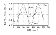
- FIG. 8 and 9 show the results of circuit simulation when the signal amplitude of the input signal Sin is small (case W1), and FIG. 9 shows waveforms of voltages Vgs1 and Vgs2 between the gate and the source.
- the voltage Vds1 is the drain-source voltage of the transistor FET1
- the voltage Vds2 is the drain-source voltage of the transistor FET2
- the voltage Vds is the voltage between the drain of the transistor FET2 and the source of the transistor FET1.
- the voltage Vgs1 is the gate-source voltage of the transistor FET1
- the voltage Vgs2 is the gate-source voltage of the transistor FET2.
- the amplitude of voltage Vgs1 and the amplitude of voltage Vgs2 are substantially the same, and the amplitude of voltage Vds1 and the amplitude of voltage Vds2 are substantially the same.
- the amplitude of voltage Vds is approximately twice the amplitude of voltages Vds1 and Vds2. That is, by setting the impedance (FIG. 7) corresponding to case W1, the power amplifier 1 can operate as expected.
- FIG. 10 and 11 show the results of circuit simulation when the signal amplitude of the input signal Sin is large (Case W2), and FIG. Reference numeral 11 denotes waveforms of voltages Vgs1 and Vgs2 between the gate and source.
- each waveform is distorted.
- the amplitude of voltage Vgs1 and the amplitude of voltage Vgs2 are substantially the same, and the amplitude of voltage Vds1 and the amplitude of voltage Vds2 are substantially the same.
- the amplitude of voltage Vds is approximately twice the amplitude of voltages Vds1 and Vds2. That is, by setting the impedance (FIG. 7) corresponding to case W2, the power amplifier 1 can perform the expected operation.
- the power amplifier 1 there are two transistors FET1 and FET2 provided on a path connecting the input terminal Tin and the output terminal Tout, and an amplitude detection circuit 20 capable of detecting the signal amplitude of the input signal Sin at the input terminal Tin. and an impedance circuit capable of changing the impedance and setting the operating conditions of the two transistors FET1 and FET2 based on the detection result of the amplitude detection circuit 20.
- the impedance circuit includes matching circuit 11, capacitor C1, inductor L2, capacitor C2, and matching circuit 13 in this example.
- the power amplifier 1 receives input signals Sin of various signal amplitudes. , it is difficult to perform the desired power amplification operation.
- the power amplifier 1 can perform a desired power amplification operation when the signal amplitude of the input signal Sin is large (case W2). power amplification operation.
- the power amplifier 1 can perform a desired power amplification operation when the signal amplitude of the input signal Sin is small (case W1). power amplification operation.
- the power amplifier 1 is equipped with an impedance circuit capable of changing the impedance and setting the operating conditions of the two transistors FET1 and FET2 based on the detection result of the amplitude detection circuit 20.
- the operating conditions of the two transistors FET1 and FET2 are set by setting the impedances of the matching circuit 11, the capacitor C1, the inductor L2, the capacitor C2, and the matching circuit 13 according to the signal amplitude. can do.
- the power amplifier 1 can perform a desired power amplification operation regardless of the signal amplitude when input signals Sin having various signal amplitudes are input.
- the amplitude detection circuit 20 has a coupler 21 for separating the AC signal Sac1 from the input signal Sin at the input terminal Tin. Amplitude is detected.
- the amplitude detection circuit 20 includes a buffer amplifier 24 having an input terminal and an output terminal connected to the coupler 21, and a diode D25 having an anode and a cathode connected to the output terminal of the buffer amplifier 24. and a capacitor C26 connected to the cathode of the diode D25, and the signal amplitude of the input signal Sin is detected based on the voltage at the capacitor C26.
- the power amplifier 1 can detect the signal amplitude of the input signal Sin with a simple configuration.
- the amplitude detection circuit has a coupler that separates the AC signal from the input signal at the input terminal, and detects the signal amplitude of the input signal by detecting the signal amplitude of this AC signal.
- the amplitude detection circuit includes a buffer amplifier having an input terminal and an output terminal connected to the coupler, a diode having an anode and a cathode connected to the output terminal of the buffer amplifier, and a cathode connected to the diode. and a capacitor for detecting the signal amplitude of the input signal based on the voltage at the capacitor. This makes it possible to detect the signal amplitude of the input signal with a simple configuration.
- FIG. 16 shows a configuration example of a power amplifier 1A according to this modified example.
- the power amplifier 1A includes a capacitor C3, an inductor L4, a transistor FET3, a capacitor C4, a resistive element R3, an inductor L5, and an impedance control circuit 14A.
- the capacitor C3 is configured to be able to change the impedance based on the control signal supplied from the impedance control circuit 14A.
- Capacitor C3, like capacitor C1, includes, for example, a plurality of capacitors, and by changing the number of capacitors used among the plurality of capacitors, the impedance can be changed.
- One end of capacitor C3 is connected to the source of transistor FET3 and inductor L4, and the other end is connected to the drain of transistor FET2 and inductor L3.
- the inductor L4 is configured to change the impedance based on the control signal supplied from the impedance control circuit 14A.
- the inductor L4 includes, for example, a plurality of inductors, and the impedance can be changed by changing the number of inductors used among the plurality of inductors.
- One end of inductor L4 is connected to the source of transistor FET3 and capacitor C3, and the other end is grounded.
- the transistor FET3 has a gate connected to the capacitor C4 and the resistance element R3, a source grounded to the capacitor C3 and the inductor L3, and a drain connected to the inductor L5 and the input terminal of the matching circuit 13.
- the capacitor C4 is configured to change the impedance based on the control signal supplied from the impedance control circuit 14A.
- Capacitor C4 like capacitor C2, includes, for example, a varactor whose impedance can be changed by changing the bias voltage of the varactor.
- One end of capacitor C4 is connected to the gate of transistor FET3 and resistance element R2, and the other end is grounded.
- a bias voltage Vg is supplied to one end of the resistance element R3, and the other end is connected to the capacitor C4 and the gate of the transistor FET3.
- the power supply voltage VDD is supplied to one end of the inductor L5, and the other end is connected to the drain of the transistor FET3 and the input terminal of the matching circuit 13.
- the power amplifier 1A uses three transistors FET1 to FET3 to perform a power amplification operation based on the input signal Sin.
- the impedance control circuit 14A detects the signal amplitude of the input signal Sin based on the input signal Sin, and based on the signal amplitude, the matching circuit 11, the capacitor C1, the inductor L2, the capacitor C2, the capacitor C3, the inductor L4, the capacitor It is configured to generate eight control signals for setting the impedance of C4 and matching circuit 13, respectively.
- the transistors FET1 to FET3 correspond to a specific example of “one or more transistors” in the present disclosure.
- the matching circuit 11, the capacitor C1, the inductor L2, the capacitor C2, the capacitor C3, the inductor L4, the capacitor C4, and the matching circuit 13 correspond to one specific example of "impedance circuit" in the present disclosure.
- the power amplifier 1A can perform a desired power amplification operation and further increase the output power when input signals having various signal amplitudes are input.
- the transistors FET1 and FET2 are provided, but the present invention is not limited to this.
- a driver amplifier may be provided in the preceding stage.
- the power amplifier 1B includes a matching circuit 41B, a driver amplifier 42B, and an impedance control circuit 14B.
- the matching circuit 41B is configured to match the impedance of the input of the driver amplifier 42B.
- Matching circuit 41B includes, for example, one or more capacitors and one or more inductors.
- the matching circuit 41B adjusts the impedance of the matching circuit 41B by changing the impedance of one or more elements of the one or more capacitors and one or more inductors based on the control signal supplied from the impedance control circuit 14B. can be changed.
- the input terminal of the matching circuit 41B is connected to the input terminal Tin of the power amplifier 1B, and the output terminal is connected to the input terminal of the driver amplifier 42B.
- the driver amplifier 42B is configured to drive the transistor FET1 through the matching circuit 11.
- the input terminal of the driver amplifier 42B is connected to the output terminal of the matching circuit 41B, and the output terminal is connected to the input terminal of the matching circuit 11B.
- the driver amplifier 42B corresponds to a specific example of "driver amplifier" in the present disclosure.
- the impedance control circuit 14B detects the signal amplitude of the input signal Sin based on the input signal Sin, and controls the matching circuit 41B, the matching circuit 11, the capacitor C1, the inductor L2, the capacitor C2, and the matching circuit based on the signal amplitude. It is configured to generate 6 control signals for setting 13 impedances respectively.
- FIG. 18 shows the appearance of a smart phone 100 to which the power amplifier of the above embodiment or the like is applied.
- This smartphone 100 is provided with a wireless communication circuit 101 that communicates with a base station.
- the wireless communication circuit 101 is applied with the power amplifier of the above embodiment.
- the power amplifiers of the above embodiments and the like can be applied to various electronic devices that perform wireless communication, such as tablet terminals, in addition to such smartphones.
- the present technology is applied to power amplifiers, but is not limited to this, and can be applied to various amplifiers.
- This technology can be configured as follows. According to the present technology having the following configuration, signals having various signal amplitudes can be amplified.
- the amplitude detection circuit has a separation element that separates an AC signal from the input signal, and is capable of detecting the signal amplitude of the input signal by detecting the signal amplitude of the AC signal. amplifier circuit.
- the amplitude detection circuit is a buffer amplifier having an input terminal connected to the isolation element and an output terminal; a diode having an anode connected to the output terminal of the buffer amplifier and a cathode; a first capacitor connected to the cathode of the diode;
- the impedance circuit includes a varactor, and can change the impedance by changing a capacitance value of the varactor based on the detection result.
- the impedance circuit has a plurality of capacitors, and can change the impedance by selecting one or a plurality of capacitors to be used from among the plurality of capacitors based on the detection result.
- the impedance circuit has a plurality of inductors, and can change the impedance by selecting one or a plurality of inductors to be used from among the plurality of inductors based on the detection result.
- the amplifier circuit according to any one of (5).
- the one or more transistors includes a first transistor and a second transistor; the first transistor has a gate connected to the input terminal and a drain; The amplifier circuit according to (1), wherein the second transistor has a gate, a drain connected to the output terminal, and a source connected to the drain of the first transistor. (8) a second capacitor connected to the gate of the second transistor and capable of changing impedance; The amplifier circuit according to (7), wherein the impedance circuit includes the second capacitor. (9) The amplifier circuit according to (7) or (8), further comprising a first inductor connected to the source of the second transistor and capable of changing impedance, wherein the impedance circuit includes the first inductor.
- (10) a third capacitor with variable impedance provided in a path connecting the drain of the first transistor and the source of the second transistor;
- (11) a first matching circuit that is provided on a path that connects the input terminal and the gate of the first transistor and that can change impedance;
- (12) a driver amplifier provided on a path connecting the input terminal and the gate of the first transistor; a first matching circuit provided on a path connecting the driver amplifier and the gate of the first transistor,
- the one or more transistors includes a final stage transistor having a drain; a second matching circuit provided on a path connecting the drain of the final stage transistor and the output terminal and capable of changing impedance;
- a communication circuit capable of wireless communication and having an amplifier circuit
- the amplifier circuit is an input terminal; an output terminal; one or more transistors provided in a path connecting the input terminal and the output terminal; an amplitude detection circuit capable of detecting the signal amplitude of the input signal at the input terminal;
- An electronic device comprising: an impedance circuit capable of changing impedance and setting operating conditions of the one or more transistors based on a detection result of the amplitude detection circuit.
Landscapes
- Engineering & Computer Science (AREA)
- Power Engineering (AREA)
- Microelectronics & Electronic Packaging (AREA)
- Amplifiers (AREA)
Abstract
Description
1.実施の形態
2.適用例
[構成例]
図1は、一実施の形態に係るパワーアンプ(パワーアンプ1)の一構成例を表すものである。パワーアンプ1は、例えば、第5世代(5G)移動通信システムにおける無線通信を行うことが可能なスマートフォンに設けられる。パワーアンプ1は、入力端子Tinと、マッチング回路11と、バイアス回路12と、抵抗素子R1と、トランジスタFET1と、インダクタL1と、キャパシタC1と、インダクタL2と、トランジスタFET2と、キャパシタC2と、抵抗素子R2と、インダクタL3と、マッチング回路13と、出力端子Toutと、インピーダンス制御回路14とを備えている。
Ids1 = gm1・Vgs1
同様に、トランジスタFET2においてドレインからソースに向かって流れる電流Ids2は、トランジスタFET2のトランスコンダクタンスgm2と、トランジスタFET2のゲート・ソース間の電圧Vgs2を用いて、以下のように表される。
Ids2 = gm2・Vgs2
続いて、本実施の形態のパワーアンプ1の動作および作用について説明する。
まず、図1を参照して、パワーアンプ1の全体動作概要を説明する。パワーアンプ1は、入力信号Sinに基づいて電力増幅動作を行うことにより、出力信号Soutを生成する。インピーダンス制御回路14は、入力信号Sinに基づいて、入力信号Sinの信号振幅を検出し、その信号振幅に基づいて、マッチング回路11、キャパシタC1、インダクタL2、キャパシタC2、およびマッチング回路13のインピーダンスをそれぞれ設定するための5つの制御信号を生成する。マッチング回路11は、インピーダンス制御回路14から供給された制御信号に基づいてインピーダンスを変更する。キャパシタC1は、インピーダンス制御回路14から供給された制御信号に基づいてインピーダンスを変更する。インダクタL2は、インピーダンス制御回路14から供給された制御信号に基づいてインピーダンスを変更する。キャパシタC2は、インピーダンス制御回路14から供給された制御信号に基づいてインピーダンスを変更する。マッチング回路13は、インピーダンス制御回路14から供給された制御信号に基づいてインピーダンスを変更する。
パワーアンプ1は、入力信号Sinの信号振幅に基づいて、マッチング回路11、キャパシタC1、インダクタL2、キャパシタC2、およびマッチング回路13のインピーダンスを変化させる。以下に、図4を参照して、キャパシタC2のインピーダンスを変化させる動作を例に挙げて説明する。
以上のように本実施の形態では、入力端子と出力端子とを結ぶ経路に設けられた2つのトランジスタと、入力端子における入力信号の信号振幅を検出可能な振幅検出回路と、インピーダンスを変更可能であり、振幅検出回路20の検出結果に基づいて、2つのトランジスタの動作条件を設定可能なインピーダンス回路とを備えるようにしたので、様々な信号振幅の入力信号が入力された場合において、信号振幅に依らずに、所望の電力増幅動作を行うことができる。
上記実施の形態では、入力信号Sinの信号振幅が小さい場合と、信号振幅が大きい場合の2つのケースに対応する2つのインピーダンス設定を設けるようにしたが、これに限定されるものではなく、これに代えて、3つ以上のインピーダンス設定を設けてもよい。
上記実施の形態では、2つのトランジスタFET1,FET2を設けたが、これに限定されるものではない。これに代えて、例えば1つのトランジスタを設けてもよいし、例えば3つ以上のトランジスタを設けてもよい。以下に、3つのトランジスタを設ける例を挙げて詳細に説明する。
上記実施の形態では、トランジスタFET1,FET2を設けたが、これに限定されるものではなく、例えば、図17に示すパワーアンプ1Bのように、この前段にドライバアンプを設けてもよい。パワーアンプ1Bは、マッチング回路41Bと、ドライバアンプ42Bと、インピーダンス制御回路14Bとを備えている。
また、これらの変形例のうちの2以上を組み合わせてもよい。
次に、上記実施の形態および変形例で説明したパワーアンプの適用例について説明する。
入力端子と、
出力端子と、
前記入力端子と前記出力端子とを結ぶ経路に設けられた1または複数のトランジスタと、
前記入力端子における入力信号の信号振幅を検出可能な振幅検出回路と、
インピーダンスを変更可能であり、前記振幅検出回路の検出結果に基づいて、前記1または複数のトランジスタの動作条件を設定可能なインピーダンス回路と
を備えた増幅回路。
(2)
前記振幅検出回路は、前記入力信号から交流信号を分離する分離素子を有し、前記交流信号の信号振幅を検出することにより前記入力信号の信号振幅を検出可能である
前記(1)に記載の増幅回路。
(3)
前記振幅検出回路は、
前記分離素子に接続された入力端子、および出力端子を有するバッファアンプと、
前記バッファアンプの前記出力端子に接続されたアノードと、カソードとを有するダイオードと、
前記ダイオードのカソードに接続された第1のキャパシタと
を有し、
前記第1のキャパシタにおける電圧に基づいて前記入力信号の信号振幅を検出可能である
前記(2)に記載の増幅回路。
(4)
前記インピーダンス回路は、バラクタを含み、前記検出結果に基づいて前記バラクタにおける容量値を変化させることにより前記インピーダンスを変更可能である
前記(1)から(3)のいずれかに記載の増幅回路。
(5)
前記インピーダンス回路は、複数のキャパシタを有し、前記検出結果に基づいて、前記複数のキャパシタのうちの使用する1または複数のキャパシタを選択することにより前記インピーダンスを変更可能である
前記(1)から(4)に記載の増幅回路。
(6)
前記インピーダンス回路は、複数のインダクタを有し、前記検出結果に基づいて、前記複数のインダクタのうちの使用する1または複数のインダクタを選択することにより前記インピーダンスを変更可能である
前記(1)から(5)のいずれかに記載の増幅回路。
(7)
前記1または複数のトランジスタは、第1のトランジスタおよび第2のトランジスタを含み、
前記第1のトランジスタは、前記入力端子に導かれたゲートと、ドレインとを有し、
前記第2のトランジスタは、ゲートと、前記出力端子に導かれたドレインと、前記第1のトランジスタのドレインに導かれたソースとを有する
前記(1)に記載の増幅回路。
(8)
前記第2のトランジスタの前記ゲートに接続され、インピーダンスを変更可能な第2のキャパシタを備え、
前記インピーダンス回路は、前記第2のキャパシタを含む
前記(7)に記載の増幅回路。
(9)
前記第2のトランジスタの前記ソースに接続され、インピーダンスを変更可能な第1のインダクタを備え
前記インピーダンス回路は、前記第1のインダクタを含む
前記(7)または(8)に記載の増幅回路。
(10)
前記第1のトランジスタの前記ドレインと前記第2のトランジスタの前記ソースとを結ぶ経路に設けられ、インピーダンスを変更可能な第3のキャパシタを備え、
前記インピーダンス回路は、前記第3のキャパシタを含む
前記(7)から(9)のいずれかに記載の増幅回路。
(11)
前記入力端子と、前記第1のトランジスタの前記ゲートとを結ぶ経路に設けられ、インピーダンスを変更可能な第1のマッチング回路を備え、
前記インピーダンス回路は、前記第1のマッチング回路を含む
前記(7)から(10)のいずれかに記載の増幅回路。
(12)
前記入力端子と、前記第1のトランジスタの前記ゲートとを結ぶ経路に設けられたドライバアンプと、
前記ドライバアンプと、前記第1のトランジスタの前記ゲートとを結ぶ経路に設けられた第1のマッチング回路と
を備え、
前記インピーダンス回路は、前記第1のマッチング回路を含む
前記(7)から(10)のいずれかに記載の増幅回路。
(13)
前記1または複数のトランジスタは、ドレインを有する最終段トランジスタを含み、
前記最終段トランジスタの前記ドレインと、前記出力端子とを結ぶ経路に設けられ、インピーダンスを変更可能な第2のマッチング回路を備え、
前記インピーダンス回路は、前記第2のマッチング回路を含む
前記(1)から(12)のいずれかに記載の増幅回路。
(14)
前記増幅回路は、パワーアンプである
前記(1)から(13)のいずれかに記載の増幅回路。
(15)
無線通信を行うことが可能であり、増幅回路を有する通信回路を備え、
前記増幅回路は、
入力端子と、
出力端子と、
前記入力端子と前記出力端子とを結ぶ経路に設けられた1または複数のトランジスタと、
前記入力端子における入力信号の信号振幅を検出可能な振幅検出回路と、
インピーダンスを変更可能であり、前記振幅検出回路の検出結果に基づいて、前記1または複数のトランジスタの動作条件を設定可能なインピーダンス回路と
を有する
電子機器。
Claims (15)
- 入力端子と、
出力端子と、
前記入力端子と前記出力端子とを結ぶ経路に設けられた1または複数のトランジスタと、
前記入力端子における入力信号の信号振幅を検出可能な振幅検出回路と、
インピーダンスを変更可能であり、前記振幅検出回路の検出結果に基づいて、前記1または複数のトランジスタの動作条件を設定可能なインピーダンス回路と
を備えた増幅回路。 - 前記振幅検出回路は、前記入力信号から交流信号を分離する分離素子を有し、前記交流信号の信号振幅を検出することにより前記入力信号の信号振幅を検出可能である
請求項1に記載の増幅回路。 - 前記振幅検出回路は、
前記分離素子に接続された入力端子、および出力端子を有するバッファアンプと、
前記バッファアンプの前記出力端子に接続されたアノードと、カソードとを有するダイオードと、
前記ダイオードのカソードに接続された第1のキャパシタと
を有し、
前記第1のキャパシタにおける電圧に基づいて前記入力信号の信号振幅を検出可能である
請求項2に記載の増幅回路。 - 前記インピーダンス回路は、バラクタを含み、前記検出結果に基づいて前記バラクタにおける容量値を変化させることにより前記インピーダンスを変更可能である
請求項1に記載の増幅回路。 - 前記インピーダンス回路は、複数のキャパシタを有し、前記検出結果に基づいて、前記複数のキャパシタのうちの使用する1または複数のキャパシタを選択することにより前記インピーダンスを変更可能である
請求項1に記載の増幅回路。 - 前記インピーダンス回路は、複数のインダクタを有し、前記検出結果に基づいて、前記複数のインダクタのうちの使用する1または複数のインダクタを選択することにより前記インピーダンスを変更可能である
請求項1に記載の増幅回路。 - 前記1または複数のトランジスタは、第1のトランジスタおよび第2のトランジスタを含み、
前記第1のトランジスタは、前記入力端子に導かれたゲートと、ドレインとを有し、
前記第2のトランジスタは、ゲートと、前記出力端子に導かれたドレインと、前記第1のトランジスタのドレインに導かれたソースとを有する
請求項1に記載の増幅回路。 - 前記第2のトランジスタの前記ゲートに接続され、インピーダンスを変更可能な第2のキャパシタを備え、
前記インピーダンス回路は、前記第2のキャパシタを含む
請求項7に記載の増幅回路。 - 前記第2のトランジスタの前記ソースに接続され、インピーダンスを変更可能な第1のインダクタを備え
前記インピーダンス回路は、前記第1のインダクタを含む
請求項7に記載の増幅回路。 - 前記第1のトランジスタの前記ドレインと前記第2のトランジスタの前記ソースとを結ぶ経路に設けられ、インピーダンスを変更可能な第3のキャパシタを備え、
前記インピーダンス回路は、前記第3のキャパシタを含む
請求項7に記載の増幅回路。 - 前記入力端子と、前記第1のトランジスタの前記ゲートとを結ぶ経路に設けられ、インピーダンスを変更可能な第1のマッチング回路を備え、
前記インピーダンス回路は、前記第1のマッチング回路を含む
請求項7に記載の増幅回路。 - 前記入力端子と、前記第1のトランジスタの前記ゲートとを結ぶ経路に設けられたドライバアンプと、
前記ドライバアンプと、前記第1のトランジスタの前記ゲートとを結ぶ経路に設けられた第1のマッチング回路と
を備え、
前記インピーダンス回路は、前記第1のマッチング回路を含む
請求項7に記載の増幅回路。 - 前記1または複数のトランジスタは、ドレインを有する最終段トランジスタを含み、
前記最終段トランジスタの前記ドレインと、前記出力端子とを結ぶ経路に設けられ、インピーダンスを変更可能な第2のマッチング回路を備え、
前記インピーダンス回路は、前記第2のマッチング回路を含む
請求項1に記載の増幅回路。 - 前記増幅回路は、パワーアンプである
請求項1に記載の増幅回路。 - 無線通信を行うことが可能であり、増幅回路を有する通信回路を備え、
前記増幅回路は、
入力端子と、
出力端子と、
前記入力端子と前記出力端子とを結ぶ経路に設けられた1または複数のトランジスタと、
前記入力端子における入力信号の信号振幅を検出可能な振幅検出回路と、
インピーダンスを変更可能であり、前記振幅検出回路の検出結果に基づいて、前記1または複数のトランジスタの動作条件を設定可能なインピーダンス回路と
を有する
電子機器。
Priority Applications (2)
| Application Number | Priority Date | Filing Date | Title |
|---|---|---|---|
| US18/559,802 US20240243711A1 (en) | 2021-05-26 | 2022-02-03 | Amplifier circuit and electronic apparatus |
| CN202280035743.5A CN117356031A (zh) | 2021-05-26 | 2022-02-03 | 放大电路和电子设备 |
Applications Claiming Priority (2)
| Application Number | Priority Date | Filing Date | Title |
|---|---|---|---|
| JP2021088784A JP2022181703A (ja) | 2021-05-26 | 2021-05-26 | 増幅回路および電子機器 |
| JP2021-088784 | 2021-05-26 |
Publications (1)
| Publication Number | Publication Date |
|---|---|
| WO2022249556A1 true WO2022249556A1 (ja) | 2022-12-01 |
Family
ID=84229677
Family Applications (1)
| Application Number | Title | Priority Date | Filing Date |
|---|---|---|---|
| PCT/JP2022/004256 Ceased WO2022249556A1 (ja) | 2021-05-26 | 2022-02-03 | 増幅回路および電子機器 |
Country Status (4)
| Country | Link |
|---|---|
| US (1) | US20240243711A1 (ja) |
| JP (1) | JP2022181703A (ja) |
| CN (1) | CN117356031A (ja) |
| WO (1) | WO2022249556A1 (ja) |
Families Citing this family (1)
| Publication number | Priority date | Publication date | Assignee | Title |
|---|---|---|---|---|
| CN120389708B (zh) * | 2025-06-26 | 2025-09-09 | 上海安其威微电子科技有限公司 | 堆叠功率放大器的分压调节电路和放大器电路 |
Citations (5)
| Publication number | Priority date | Publication date | Assignee | Title |
|---|---|---|---|---|
| WO2008044276A1 (en) * | 2006-10-06 | 2008-04-17 | Panasonic Corporation | Electric power amplifying apparatus |
| JP2011069924A (ja) * | 2009-09-24 | 2011-04-07 | Nippon Telegr & Teleph Corp <Ntt> | Qpsk変調器 |
| WO2012020476A1 (ja) * | 2010-08-10 | 2012-02-16 | パイオニア株式会社 | インピーダンス整合装置、制御方法 |
| JP2013211830A (ja) * | 2012-03-01 | 2013-10-10 | Sony Corp | 増幅器および無線通信装置 |
| JP2014045371A (ja) * | 2012-08-27 | 2014-03-13 | Fujitsu Ltd | 電力増幅装置 |
Family Cites Families (1)
| Publication number | Priority date | Publication date | Assignee | Title |
|---|---|---|---|---|
| US8611834B2 (en) * | 2010-11-01 | 2013-12-17 | Cree, Inc. | Matching network for transmission circuitry |
-
2021
- 2021-05-26 JP JP2021088784A patent/JP2022181703A/ja active Pending
-
2022
- 2022-02-03 US US18/559,802 patent/US20240243711A1/en active Pending
- 2022-02-03 WO PCT/JP2022/004256 patent/WO2022249556A1/ja not_active Ceased
- 2022-02-03 CN CN202280035743.5A patent/CN117356031A/zh not_active Withdrawn
Patent Citations (5)
| Publication number | Priority date | Publication date | Assignee | Title |
|---|---|---|---|---|
| WO2008044276A1 (en) * | 2006-10-06 | 2008-04-17 | Panasonic Corporation | Electric power amplifying apparatus |
| JP2011069924A (ja) * | 2009-09-24 | 2011-04-07 | Nippon Telegr & Teleph Corp <Ntt> | Qpsk変調器 |
| WO2012020476A1 (ja) * | 2010-08-10 | 2012-02-16 | パイオニア株式会社 | インピーダンス整合装置、制御方法 |
| JP2013211830A (ja) * | 2012-03-01 | 2013-10-10 | Sony Corp | 増幅器および無線通信装置 |
| JP2014045371A (ja) * | 2012-08-27 | 2014-03-13 | Fujitsu Ltd | 電力増幅装置 |
Also Published As
| Publication number | Publication date |
|---|---|
| CN117356031A (zh) | 2024-01-05 |
| JP2022181703A (ja) | 2022-12-08 |
| US20240243711A1 (en) | 2024-07-18 |
Similar Documents
| Publication | Publication Date | Title |
|---|---|---|
| US11855586B2 (en) | Power amplifier module | |
| JP6680235B2 (ja) | 電力増幅回路および高周波モジュール | |
| US7444124B1 (en) | Adjustable segmented power amplifier | |
| JP5879547B2 (ja) | スルーモード付き低雑音増幅器 | |
| JP4305472B2 (ja) | 差動増幅器 | |
| KR101719310B1 (ko) | 듀얼 동작 모드 전력 증폭기 | |
| KR101133416B1 (ko) | 캐스코드 증폭기용 피드백 바이어싱을 이용한 전력 전송 시스템 | |
| JP5979160B2 (ja) | 増幅器 | |
| US7560990B2 (en) | Low noise amplifier and low noise amplifying method | |
| US20190131936A1 (en) | High and low voltage limited power amplification system | |
| US20070069821A1 (en) | Active balun device | |
| US20130127528A1 (en) | Power amplifier and amplification method thereof | |
| CN113508526B (zh) | 用于优化共源共栅放大器中三阶截取点的晶体管偏置调整 | |
| US6897732B2 (en) | Amplifier | |
| US20070188226A1 (en) | Power amplifier input structure having a differential output | |
| CN116918250A (zh) | 具有自适应退化反馈模拟预失真的功率放大器 | |
| US10320441B2 (en) | Systems and methods for a switchless radio front end | |
| CN113162561A (zh) | 用于对放大器的线性度进行补偿的前置补偿器 | |
| US20060244529A1 (en) | Input structure for a power amplifier and associated methods | |
| US8704600B2 (en) | Power amplifier | |
| JP2008516510A (ja) | デュアルバイアス制御回路 | |
| WO2022249556A1 (ja) | 増幅回路および電子機器 | |
| US7724039B2 (en) | Conversion circuit for converting differential signal into signal-phase signal | |
| US11146218B2 (en) | Amplification circuit | |
| US11437965B2 (en) | Variable gain amplifier and wireless communication device |
Legal Events
| Date | Code | Title | Description |
|---|---|---|---|
| 121 | Ep: the epo has been informed by wipo that ep was designated in this application |
Ref document number: 22810842 Country of ref document: EP Kind code of ref document: A1 |
|
| WWE | Wipo information: entry into national phase |
Ref document number: 18559802 Country of ref document: US |
|
| WWE | Wipo information: entry into national phase |
Ref document number: 202280035743.5 Country of ref document: CN |
|
| NENP | Non-entry into the national phase |
Ref country code: DE |
|
| 122 | Ep: pct application non-entry in european phase |
Ref document number: 22810842 Country of ref document: EP Kind code of ref document: A1 |