WO2022239701A1 - はんだ粒子の分級方法、はんだ粒子、はんだ粒子の分級システム、接着剤組成物、及び接着剤フィルム - Google Patents
はんだ粒子の分級方法、はんだ粒子、はんだ粒子の分級システム、接着剤組成物、及び接着剤フィルム Download PDFInfo
- Publication number
- WO2022239701A1 WO2022239701A1 PCT/JP2022/019535 JP2022019535W WO2022239701A1 WO 2022239701 A1 WO2022239701 A1 WO 2022239701A1 JP 2022019535 W JP2022019535 W JP 2022019535W WO 2022239701 A1 WO2022239701 A1 WO 2022239701A1
- Authority
- WO
- WIPO (PCT)
- Prior art keywords
- solder particles
- solder
- particles
- electrode
- opening
- Prior art date
- Legal status (The legal status is an assumption and is not a legal conclusion. Google has not performed a legal analysis and makes no representation as to the accuracy of the status listed.)
- Ceased
Links
Images


Classifications
-
- B—PERFORMING OPERATIONS; TRANSPORTING
- B07—SEPARATING SOLIDS FROM SOLIDS; SORTING
- B07B—SEPARATING SOLIDS FROM SOLIDS BY SIEVING, SCREENING, SIFTING OR BY USING GAS CURRENTS; SEPARATING BY OTHER DRY METHODS APPLICABLE TO BULK MATERIAL, e.g. LOOSE ARTICLES FIT TO BE HANDLED LIKE BULK MATERIAL
- B07B13/00—Grading or sorting solid materials by dry methods, not otherwise provided for; Sorting articles otherwise than by indirectly controlled devices
- B07B13/04—Grading or sorting solid materials by dry methods, not otherwise provided for; Sorting articles otherwise than by indirectly controlled devices according to size
-
- B—PERFORMING OPERATIONS; TRANSPORTING
- B03—SEPARATION OF SOLID MATERIALS USING LIQUIDS OR USING PNEUMATIC TABLES OR JIGS; MAGNETIC OR ELECTROSTATIC SEPARATION OF SOLID MATERIALS FROM SOLID MATERIALS OR FLUIDS; SEPARATION BY HIGH-VOLTAGE ELECTRIC FIELDS
- B03C—MAGNETIC OR ELECTROSTATIC SEPARATION OF SOLID MATERIALS FROM SOLID MATERIALS OR FLUIDS; SEPARATION BY HIGH-VOLTAGE ELECTRIC FIELDS
- B03C7/00—Separating solids from solids by electrostatic effect
- B03C7/02—Separators
Definitions
- the present disclosure relates to a solder particle classification method, solder particles, a solder particle classification system, an adhesive composition, and an adhesive film.
- Solder paste which is a mixture of solder particles and paste-like flux, is used in surface mounting technology for mounting electronic devices on printed wiring boards. Spherical particles having a diameter of about 100 ⁇ m or more are generally used as the solder particles.
- solder particles are produced by various methods, and studies have been made to suppress variations in particle size in various production methods (see, for example, Patent Document 1 below).
- the present disclosure aims to provide a method for classifying solder particles, solder particles, a system for classifying solder particles, and an adhesive composition and adhesive film containing solder particles.
- a first electrode having a static dissipative or conductive placement portion, and an insulation property provided with a plurality of openings facing the placement portion and opening toward the placement portion side.
- Solder particles P arranged in the arrangement portion by forming an electric field between the first electrode and the second electrode of the electrostatic attraction device, a first step of electrostatically attracting the solder particles P2 to the attracting portion; a second step of removing the solder particles P2 that are attracted to the attracting portion and not accommodated in the opening from the attracting portion; and a third step of collecting the solder particles P1 contained in a part, wherein the average particle diameter of the solder particles P is 10 ⁇ m or more.
- the second step can efficiently remove solder particles having a large particle size that are not accommodated in the openings, and the dispersity of the recovered solder particles P1 can be made smaller than that of the solder particles P. can be done. This makes it possible to obtain solder particles with a small CV value (coefficient of variation of particle size) of the particle size. Further, according to the above method, the average particle size of the collected solder particles P1 can be easily changed by adjusting the opening size of the opening.
- the solder particles P may have a particle diameter of less than 10 ⁇ m at a rate of 30% or less.
- MDp/OD satisfies 0.5 to 1.5, where MDp ( ⁇ m) is the average particle diameter of the solder particles P and OD ( ⁇ m) is the opening diameter of the opening. can be anything.
- solder particles having an average particle diameter of 10 to 100 ⁇ m, a particle diameter CV value of 3 to 15%, and an average sphericity of 0.90 or more.
- Each of the above solder particles has the above configuration, so that it is possible to maintain a constant gap between the electrode and the wiring during mounting in surface mounting, and to meet the demand for suppressing gap variation in each wiring. It can be said that the method of classifying solder particles described above is excellent in productivity in that it can be manufactured from solder particles manufactured by a normal method.
- the above solder particles may have an average particle size of 10 to 50 ⁇ m.
- Another aspect of the present disclosure relates to an adhesive composition that includes an adhesive component and the solder particles described above.
- Another aspect of the present disclosure relates to an adhesive film containing an adhesive component and the solder particles described above.
- Another aspect of the present disclosure is an insulation provided with a first electrode having a static dissipative or conductive placement portion, and a plurality of openings facing the placement portion and opening on the placement portion side a second electrode having an adsorption portion having a property; a removing means for removing from the adsorption portion the solder particles that are adsorbed to the adsorption portion and are not accommodated in the opening;
- the present invention relates to a solder particle classification system comprising a recovery means for recovering solder particles contained in an opening of an adsorption section.
- solder particle classification method described above can be implemented, and solder particles with a small particle diameter CV value (particle diameter variation coefficient) can be obtained. Also, by adjusting the opening diameter of the opening, the average particle diameter of the obtained solder particles can be easily changed. Therefore, the solder particle classification system described above can also be applied as a monodisperse solder particle production system.
- solder particle classification method solder particles, a solder particle classification system, and an adhesive composition and adhesive film containing solder particles.
- FIG. 2(a) is a plan view schematically showing an example of the adsorption portion
- FIG. 2(b) is a sectional view taken along line Ib--Ib of FIG. 2(a).
- FIG. 4 is a schematic diagram for explaining a method of classifying solder particles;
- FIG. 4 is a schematic diagram for explaining a method of classifying solder particles;
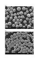
- SEM images of Solder Particle-1 and Solder Particle-2. 4 shows SEM images of solder particles before and after classification in Example 1.
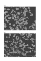
- FIG. 4 is SEM images of solder particles before and after classification in Comparative Example 1.
- FIG. 4 is SEM images of solder particles before and after classification in Comparative Example 1.
- the upper limit value or lower limit value of the numerical range at one stage may be replaced with the upper limit value or lower limit value of the numerical range at another stage.
- the upper and lower limits of the numerical ranges may be replaced with the values shown in the examples.
- a collection of a plurality of particles is also referred to herein as a "particle".
- the solder particle classification method of the present embodiment includes a first electrode having a static dissipative or conductive placement portion, and a plurality of openings facing the placement portion and opening on the placement portion side. and a second electrode having an insulating adsorption portion, and an electrostatic adsorption device having an electrostatic adsorption device, wherein an electric field is formed between the first electrode and the second electrode of the electrostatic adsorption device.
- a first step of electrostatically attracting the solder particles P in the attracting portion a second step of removing the solder particles P2 that are attracted to the attracting portion and not accommodated in the opening; and a third step of collecting the solder particles P1 accommodated in the opening.
- FIG. 1 is a diagram showing a schematic configuration of an electrostatic adsorption device used in the solder particle classification method of the present embodiment.
- the electrostatic adsorption device 1 includes a lower electrode (first electrode) 2 having an arrangement portion 2a, and an upper electrode having an adsorption portion 4 arranged above the arrangement portion 2a in the direction of gravity and facing the arrangement portion 2a. (second electrode) 3; Solder particles P are arranged in the arrangement portion 2a.
- the arrangement portion 2a shown in FIG. 1 is integrated with the lower electrode main body and is the surface on the upper electrode 3 side.
- the placement portion 2a may be provided separately on the surface of the lower electrode 2 on the upper electrode 3 side.
- a material having static electricity dissipative property or conductivity can be used as a material for the lower electrode 2.
- a material having a surface resistivity of 10 13 ⁇ or less can be used, and specific examples include metals and glass.
- the shape of the lower electrode 2 is not particularly limited, but may be, for example, a flat plate shape, a roll shape, or the like.
- a material having electrostatic dissipative properties or conductivity can be used as the material of the placement portion 2a provided on the surface of the lower electrode 2 on the side of the upper electrode 3.
- a material having electrostatic dissipative properties or conductivity can be used as the material of the placement portion 2a provided on the surface of the lower electrode 2 on the side of the upper electrode 3.
- a material having electrostatic dissipative properties or conductivity can be used.
- a material having a surface resistivity of 10 13 ⁇ or less can be used, and specific examples include metal, glass, and conductive resin such as conductive polytetrafluoroethylene (PTFE).
- the shape of the placement portion 2a is not particularly limited as long as it can place the solder particles. For example, it may have a shape that has a bottom surface and a side surface and is open in the direction of the adsorption section.
- the static electricity dissipative placement portion may have a surface resistivity of 10 13 ⁇ or less, or 10 6 ⁇ or more.
- the conductive placement portion may have a surface resistivity of 10 6 ⁇ or less, or 10 ⁇ 3 ⁇ or more.
- the electrode body constituting the upper electrode 3 one having static electricity dissipative properties or conductivity can be used.
- a material having a surface resistivity of 10 13 ⁇ or less can be used, and specific examples include metals and glass.
- the shape of the electrode body is not particularly limited, but may be, for example, a flat plate shape or a roll shape.
- the adsorption section 4 is provided with a plurality of openings 10 that open toward the placement section.
- the openings 10 may be provided in a predetermined pattern.
- An insulating material can be used as the material of the adsorption part 4 .
- materials with surface resistivities greater than 10 13 ⁇ can be used.
- the shape of the adsorption portion 4 is not particularly limited as long as it has the above-described opening. It may be a film that can be separated from the electrode body.
- FIG. 2 is a plan view schematically showing an example of a suction portion
- (b) of FIG. 2 is a cross-sectional view taken along line Ib-Ib of (a) of FIG.
- the suction portion 4 shown in FIG. 2A is provided with a plurality of openings (recesses) 10 having a predetermined pattern (opening pattern).
- the predetermined pattern (opening pattern) may be a regular arrangement or an irregular arrangement.
- the opening 10 of the suction portion 4 may be tapered such that the opening area increases from the bottom portion 10a side of the opening portion 10 toward the surface 4a side of the suction portion 4 . That is, as shown in FIGS. 2A and 2B, the width of the bottom portion 10a of the opening 10 (the width a in FIGS. 2A and 2B) (Width b in (a) and (b) of FIG. 2 (hereinafter also referred to as "opening diameter" of the opening). Then, the size of the opening 10 (width a, width b, volume, taper angle, depth, etc.) may be set according to the size of the solder particles to be accommodated.
- the width b (opening diameter) of the opening can be appropriately set so that the average particle diameter of the collected solder particles P1 is within a predetermined range.
- the width b (opening diameter) of the opening can be 5 to 120 ⁇ m, 6 to 120 ⁇ m, or 7 to 120 ⁇ m.
- the width b (opening diameter) of the opening can be appropriately set so that the average particle diameter of the collected solder particles P1 is within a predetermined range. Further, from the viewpoint of improving recovery efficiency, MDp/OD satisfies 0.5 to 1.5, where MDp ( ⁇ m) is the average particle diameter of the solder particles P and OD ( ⁇ m) is the opening diameter of the opening. may satisfy 0.75 to 1.25, or may satisfy 0.9 to 1.1.
- the shape of the opening 10 may be a shape other than the shapes shown in FIGS. 2(a) and 2(b).
- the shape of the openings on the surface 4a may be elliptical, triangular, quadrangular, polygonal, etc., in addition to circular.
- the bottom portion 10a may also have a shape other than a flat surface, such as a mountain shape, a valley shape, an aggregate of fine protrusions, or the like. From the viewpoint of increasing the average sphericity of the solder particles P1, the shape of the opening may be circular, elliptical, triangular, quadrangular, or polygonal.
- the solder particles P1 accommodated in the opening of the adsorption portion may not be wholly accommodated in the opening, and may be in a state in which a portion of the solder particles protrude from the surface 4a of the adsorption portion. .
- 2/3 or less of the particle diameter of the particles may protrude, or 1/2 or less of the particle diameter may protrude.
- the adsorption portion 4 As materials for forming the adsorption portion 4, for example, inorganic materials such as silicon, various ceramics, glass, metals such as stainless steel, and organic materials such as various resins can be used.
- the opening 10 of the adsorption section can be formed by known methods such as photolithography, nanoimprinting, machining, electron beam processing, and radiation processing.
- the adsorption part 4 may be a single layer, or may be composed of a plurality of layers such as a laminate of a base layer and an opening layer provided with an opening.
- the adsorption part 4 is a laminate, for example, it is a film provided with an opening layer formed on a base layer such as PET using a photocurable resin composition by a method such as photolithography or nanoimprinting. good too.
- the lower electrode 2 and the upper electrode 3 are arranged with a predetermined distance therebetween, and the distance D1 between the electrodes can be 0.5 to 100 mm, preferably 1 to 20 mm. may be 2 to 15 mm.
- the lower electrode 2 may be movable, in which case the solder particles can be easily supplied continuously.
- the bottom electrode can be provided on the surface of a belt or cylindrical roller.
- the upper electrode 3 may be movable, and in this case, it becomes easy to continuously supply the adsorption portions for adsorbing the solder particles.
- the upper electrode can be provided on the surface of a belt or cylindrical roller.
- the power supply 5 may be anything that can form an electric field between the lower electrode and the upper electrode, and for example, a known high voltage power supply can be used.
- the high voltage power supply may be a DC power supply or an AC power supply.
- the control unit 6 can have functions such as adjustment of applied voltage and application time, for example.
- solder particles P to be arranged in the arrangement portion solder particles manufactured by a known method can be used, and commercially available products such as micro solder balls may be used.
- Solder particles may comprise, for example, tin or a tin alloy.
- tin alloy for example, In—Sn alloy, In—Sn—Ag alloy, Sn—Au alloy, Sn—Bi alloy, Sn—Bi—Ag alloy, Sn—Ag—Cu alloy, Sn—Cu alloy, etc. are used. be able to. Specific examples of these tin alloys include the following examples.
- Solder particles may include, for example, indium or an indium alloy.
- the indium alloy for example, an In--Bi alloy, an In--Ag alloy, or the like can be used. Specific examples of these indium alloys include the following examples. ⁇ In-Bi (In66.3% by mass, Bi33.7% by mass, melting point 72° C.) ⁇ In-Bi (In 33.0% by mass, Bi 67.0% by mass, melting point 109 ° C.) ⁇ In-Ag (97.0% by mass of In, 3.0% by mass of Ag, melting point 145°C)
- the solder particles may further contain one or more selected from Ag, Cu, Ni, Bi, Zn, Pd, Pb, Au, P and B.
- the shape of the solder particles P may be spherical or substantially spherical, or may be non-spherical such as scale-like or elliptical (rugby ball)-like.
- solder particles P solder particles with an average particle diameter of 10 ⁇ m or more can be used.
- the solder particles P arranged in the arrangement portion can sufficiently contain solder particles that are present as single particles without agglomeration, and the CV value of the particle diameter of the collected solder particles P1 is can be easily reduced.
- the average particle size of solder particles is obtained by randomly measuring the particle size of 100 solder particles using a digital caliper from a photograph taken with a scanning electron microscope (SEM) and averaging them.
- SEM scanning electron microscope
- the CV value of the particle size of the solder particles is calculated by dividing the standard deviation of the particle size measured by the above method by the average particle size and multiplying by 100.
- the proportion of particles having a particle diameter of less than 10 ⁇ m in the solder particles P may be 50% or less, or 30% or less. , may be 20% or less, or 10% or less, and may not contain particles having a particle diameter of less than 10 ⁇ m.
- Percentage means the ratio (percentage) based on the number. For example, the ratio of particles with a particle diameter of less than 10 ⁇ m is obtained as follows. First, the particle diameters of 100 solder particles are randomly measured using a digital vernier caliper from a photograph taken by an SEM. By counting the number of particles with a particle diameter of less than 10 ⁇ m, dividing this number by the total number (100) and multiplying by 100, the proportion of particles with a particle diameter of less than 10 ⁇ m can be obtained. When the solder particles have a shape other than a spherical shape, the particle size is defined as the longest diameter of the solder particles.
- the solder particles P may be previously treated to remove solder particles with a particle size of less than 10 ⁇ m by a known classification method such as dry classification with a sieve and sedimentation classification.
- the proportion of particles having a particle diameter of 30 ⁇ m or more in the solder particles P may be 50% or less, or 40% or less. It may be 30% or less, and may not contain particles with a particle diameter of 30 ⁇ m or more.
- the solder particles P may be previously treated to remove solder particles with a particle size of 30 ⁇ m or more by a known classification method such as dry classification with a sieve or sedimentation classification.
- the solder particles P have an average sphericity of 0.1 or more, 0.3 or more, 0.5 or more, 0.7 or more, 0.8 or more, 0.85 or more, 0.1 to 0.8, or 0.1 to 0.8. It may be from 5 to 0.85.
- the average sphericity of solder particles is obtained by randomly measuring the longest diameter and minimum diameter of 100 solder particles using a digital vernier caliper from a photograph taken with an SEM, and calculating the sphericity defined by the following formula. , which is obtained by averaging them.
- Sphericality Dmin / Dmax [In the formula, D max indicates the maximum particle diameter ( ⁇ m), and D min indicates the minimum particle diameter ( ⁇ m). ]
- the average particle size of the solder particles P1 is 10 to 100 ⁇ m, 10 to 80 ⁇ m, 10 to 50 ⁇ m, 10 to 40 ⁇ m, 10 to 35 ⁇ m, 10 to 30 ⁇ m, 15 to 100 ⁇ m, 15 to 50 ⁇ m, 15 to 35 ⁇ m, 30 to 70 ⁇ m, 50 It may be ⁇ 80 ⁇ m, 50-100 ⁇ m, or 70-100 ⁇ m.
- the CV value of the particle diameter of the solder particles P1 may be 1% to 20%, 2% to 18%, or 3% to 15%.
- the solder particles P1 may have an average sphericity of 0.90 or more, 0.92 or more, 0.95 or more, 0.98 or more, or 0.985 or more.
- FIG. 3 is a schematic diagram for explaining the solder particle classification method of the present embodiment.
- (a) of FIG. 3 shows a state in which solder particles P are arranged in the arrangement portion.
- the solder particles P charged to the opposite polarity to that of the upper electrode in the placement portion rise due to electrostatic attraction.
- the rising solder particles P are electrostatically attracted to the attraction portion.
- the solder particles electrostatically attracted to the attraction portion are divided into solder particles P1 accommodated in the openings and solder particles P2 not accommodated in the openings.
- solder particles that are adsorbed to the opening but are not accommodated are Included in the solder particles P2.
- the electric field strength to be applied may be 0.1 to 30 kV/cm, may be 0.2 to 30 kV/cm, or may be 0.5 to 20 kV/cm.
- the application of the electric field may be continuous or intermittent.
- the application time of the electric field can be appropriately set according to the amount of solder particles to be adsorbed by the adsorption portion.
- the electrostatic attraction of the solder particles can be stopped when the solder particles are sufficiently attracted to the attraction part 4 due to the effect of reducing the electric field due to the attraction of the solder particles to the insulation attraction part 4 . . That is, since the intensity of the electric field between the lower electrode 2 and the upper electrode 3 becomes smaller as the solder particles adhere to the adsorption portion 4, the electric field between the electrodes is reduced in addition to the disappearance of the solder particles in the arrangement portion. By making it sufficiently small, it is also possible to stop the jumping of solder particles.
- solder particles can be supplied by making the lower electrode 2 movable or by replenishing the solder particles to the arrangement portion, the solder can be applied until the electric field becomes sufficiently weak. Particles can be adsorbed on the adsorption part.
- the first electrode and the second electrode are arranged on the lower side and the upper side with respect to the direction of gravity, respectively.
- the direction of movement may be horizontal or may be inclined with respect to the direction of gravity.
- the first electrode and the second electrode can be configured in the same manner as described above.
- solder particles P2 Surplus particles
- Methods for removing excess particles include physical removal means such as air blow, brush, and squeegee, and electrostatic removal means such as ionizers.
- FIG. 4 is a schematic diagram for explaining the solder particle classification method of the present embodiment.
- FIG. 4( a ) shows a mode in which the solder particles P ⁇ b>2 adsorbed to the adsorption portion 4 and not accommodated in the opening 10 are removed by the air blow 20 .
- the removed surplus particles may be collected and recycled.
- solder particles P1 accommodated in the openings are recovered from the adsorption portion that has passed through the second step.
- Methods of collection include ultrasonic dispersion, wind force collection, and particle collection by impact on the adsorption part.
- the adsorption part 4 is immersed in a liquid 24 such as an arbitrary organic solvent in an ultrasonic dispersion device 22, and the solder particles P1 contained in the openings 10 are dispersed into the liquid 24 by ultrasonic waves.
- a distributed mode is shown.
- the solder particles P1 can be collected through the third step.
- the collected solder particles P1 may be used as they are as solder particles with a reduced CV value of the particle diameter, or may be used by being mixed with other solder particles.
- the collected solder particles P1 can also be subjected to another classification process.
- the method of classifying solder particles according to the present embodiment can reduce problems such as a decrease in productivity due to clogging and damage to the surface of solder particles, which are likely to occur in a method of classifying particles using a sieve.
- solder particle classification method of the present embodiment it is possible to manufacture solder particles having a desired average particle size and a reduced particle size CV value. That is, the method for classifying solder particles according to the present embodiment can be used as a method for producing low-dispersion or monodisperse solder particles.
- solder particle classification method of the present embodiment it is possible to manufacture solder particles having a desired average particle size, a reduced CV value of the particle size, and an increased average sphericity. can. That is, the method for classifying solder particles according to the present embodiment can be used as a method for producing solder particles with low dispersion and high sphericity.
- solder particles have an average particle size of 10 to 100 ⁇ m and a CV value of the particle size of 1 to 30%.
- the solder particles of this embodiment may have an average particle diameter of 10 to 30 ⁇ m and a CV value of the particle diameter of 3 to 15%.
- the solder particles of this embodiment may have an average particle size of 30 to 70 ⁇ m and a CV value of the particle size of 3 to 15%.
- the solder particles of this embodiment may have an average particle diameter of 70 to 100 ⁇ m and a CV value of the particle diameter of 3 to 15%.
- the solder particles of the present embodiment may have an average particle diameter of 10 to 100 ⁇ m, a CV value of the particle diameter of 3 to 15%, and an average sphericity of 0.90 or more.
- the solder particles of the present embodiment may have an average particle diameter of 10 to 50 ⁇ m, a CV value of the particle diameter of 3 to 15%, and an average sphericity of 0.90 or more.
- solder particles has the above configuration, so that the electrode-wiring gap at the time of mounting in surface mounting can be maintained constant, and it is possible to meet the demand for suppressing gap variation in each wiring.
- the method of classifying solder particles according to the present embodiment can be said to be excellent in productivity in that it can be manufactured from solder particles manufactured by a normal method.
- solder particles of this embodiment can be the same as those of the solder particles P described above.
- the solder particles of the present embodiment have an average particle diameter of 10 to 100 ⁇ m, 10 to 80 ⁇ m, 10 to 50 ⁇ m, 10 to 40 ⁇ m, 10 to 35 ⁇ m, 10 to 30 ⁇ m, 15 ⁇ 100 ⁇ m, 15-50 ⁇ m, 15-35 ⁇ m, 30-70 ⁇ m, 50-80 ⁇ m, 50-100 ⁇ m, or 70-100 ⁇ m, and the CV value of the particle size is 1%-20%, 2%-18% , or 3% to 15%.
- the solder particles of the present embodiment may have an average sphericity of 0.90 or more, 0.92 or more, 0.95 or more, 0.98 or 0.985 or more.
- the average sphericity is within the above range, the solder particles trapped between the electrodes during mounting or the solder bumps formed on the electrodes are less likely to have height variations, and solder particles that do not participate in connection are less likely to occur. can be further reduced.
- sedimentation classification and mesh classification are known as general classification methods, these methods cannot obtain solder particles having the above average sphericity for the following reasons. That is, since sedimentation classification is classified by specific gravity, precise classification from the viewpoint of shape (sphericity) cannot be performed, and mesh classification is classification using a mesh, so particles with a high aspect ratio (for example, rugby Ball-shaped particles, etc.) also pass through the mesh, so precise classification from the viewpoint of shape (sphericity) cannot be performed.
- the solder classification system of the present embodiment includes a first electrode having a static dissipative or conductive placement portion, and an insulation electrode provided with a plurality of openings facing the placement portion and opening toward the placement portion. a second electrode having an adsorption portion having a property; a removing means for removing from the adsorption portion the solder particles that are adsorbed to the adsorption portion and are not accommodated in the opening; collecting means for collecting the solder particles accommodated in the opening of the adsorption portion.
- the electrostatic adsorption device, removal means, and recovery means can be configured in the same manner as those used in the solder particle classification method described above.
- solder particle classification method described above can be implemented, and solder particles with a small particle diameter CV value (particle diameter variation coefficient) can be obtained. Also, by adjusting the opening diameter of the opening, the average particle diameter of the obtained solder particles can be easily changed. Therefore, the solder particle classification system described above can also be applied as a monodisperse solder particle production system.
- the adhesive composition of this embodiment includes an adhesive component and the solder particles of this embodiment described above.
- Adhesive components include monomers (main agent) and curing agents.
- a cationically polymerizable compound, an anionically polymerizable compound, or a radically polymerizable compound can be used as the monomer.
- Examples of cationic polymerizable compounds or anionically polymerizable compounds include epoxy compounds.
- epoxy compounds include bisphenol-type epoxy resins derived from epichlorohydrin and bisphenol compounds such as bisphenol A, bisphenol F, and bisphenol AD; Resins and various epoxy compounds having two or more glycidyl groups in one molecule such as glycidylamine, glycidyl ether, biphenyl, and alicyclic can be used.
- the epoxy-based compound may be an oligomer.
- radically polymerizable compound a compound having a functional group that polymerizes by radicals can be used, and examples thereof include acrylic compounds such as (meth)acrylate, maleimide compounds, and styrene derivatives.
- the radically polymerizable compound can be used in either a monomer or oligomer state, and a mixture of monomer and oligomer may be used. That is, the term "monomer” as used herein also includes oligomers.
- the monomers may be used singly or in combination of two or more.
- the curing agent includes imidazole-based, hydrazide-based, boron trifluoride-amine complex, sulfonium salt, onium salt, pyridium salt, amine imide, polyamine salt, dicyandiamide, acid anhydride, and the like. It is preferable that these curing agents are microencapsulated by being coated with a polyurethane-based or polyester-based polymer substance or the like in order to extend the pot life.
- the curing agent used in combination with the epoxy compound is appropriately selected according to the desired connection temperature, connection time, storage stability, etc.
- the curing agent may have a gel time of 10 seconds or less at a predetermined temperature when the composition containing the epoxy compound and the curing agent is used. From the point of view, there may be no difference in gel time from the composition after storage in a constant temperature bath at 40° C. for 10 days. From this point of view, the curing agent may be a sulfonium salt.
- curing agents such as peroxide compounds and azo compounds, which are decomposed by heating to generate free radicals, can be used.
- the curing agent used in combination with the acrylic compound is appropriately selected according to the desired connection temperature, connection time, storage stability, etc.
- the curing agent may be an organic peroxide or an azo compound having a half-life of 10 hours at a temperature of 40° C. or higher and a half-life of 1 minute at a temperature of 180° C. or lower.
- the curing agent may be used singly or in combination of two or more.
- the adhesive composition may further contain a decomposition accelerator, inhibitor, and the like.
- the blending amount of the curing agent is determined from the viewpoint of obtaining a sufficient reaction rate when using either an epoxy-based compound or an acrylic-based monomer. 0.1 parts by mass or more and 40 parts by mass or less, or 1 part by mass or more and 35 parts by mass or less with respect to 100 parts by mass in total with the material.
- the amount of the curing agent is 0.1 parts by mass or more, a sufficient reaction rate can be obtained, and good adhesive strength and low connection resistance can be easily obtained. It becomes easy to prevent the fluidity of the composition from decreasing and the connection resistance from increasing, and it becomes easy to ensure the storage stability of the adhesive composition.
- the film-forming material is preferably a polymer that has the effect of facilitating the handling of the low-viscosity composition containing the monomer and curing agent.
- the film-forming material it is possible to prevent the film from being easily torn, cracked, or sticky, and it is possible to obtain an adhesive film such as an anisotropically conductive film that is easy to handle.
- the adhesive composition of this embodiment may further contain a film-forming material.
- thermoplastic resin can be suitably used as the film-forming material.
- examples thereof include phenoxy resins, polyvinyl formal resins, polystyrene resins, polyvinyl butyral resins, polyester resins, polyamide resins, xylene resins, polyurethane resins, polyacrylic resins, and polyester urethane resins. These polymers may contain siloxane bonds or fluorine substituents.
- phenoxy resins can be used from the viewpoint of adhesive strength, compatibility, heat resistance, and mechanical strength.
- thermoplastic resins may be used singly or in combination of two or more.
- the weight average molecular weight of the thermoplastic resin may be 5,000 or more and 150,000 or less, or 10,000 or more and 80,000 or less. When the weight average molecular weight of the thermoplastic resin is 5,000 or more, good film formability is likely to be obtained, and when it is 150,000 or less, good compatibility with other components is likely to be obtained.
- the weight average molecular weight of a thermoplastic resin refers to a value measured using a standard polystyrene calibration curve from a gel permeation chromatograph (GPC) under the following conditions.
- GPC gel permeation chromatograph
- the blending amount of the film-forming material may be 5% by mass or more and 80% by mass or less, or may be 15% by mass or more and 70% by mass or less, based on the total amount of the monomer, curing agent, and film-forming material.
- amount of the film-forming agent is 5% by mass or more, good film-forming properties can be easily obtained, and when the amount is 80% by mass or less, the adhesive composition tends to exhibit good fluidity.
- the content of the solder particles in the adhesive composition of the present embodiment may be in the range of 5 to 80 parts by volume with respect to 100 parts by volume of the total amount of the adhesive composition, and may be 10 to 70 parts by volume. .
- the content of the solder particles may be 5 to 80% by mass, 10 to 70% by mass, or 20 to 60% by mass based on the total amount of the adhesive composition.
- the adhesive composition may further contain other additives such as fillers, softeners, accelerators, antioxidants, colorants, flame retardants, thixotropic agents, and coupling agents.
- additives such as fillers, softeners, accelerators, antioxidants, colorants, flame retardants, thixotropic agents, and coupling agents.
- an adhesive film such as an anisotropic conductive film can be produced.
- the adhesive film of this embodiment includes an adhesive component and the solder particles of this embodiment described above.
- the adhesive film can have the same composition as the adhesive composition of this embodiment described above.
- the adhesive film of this embodiment can be produced by the following method.
- a varnish composition (varnish-like adhesive composition) is prepared by stirring, mixing or kneading the adhesive composition of the present embodiment in an organic solvent. After that, the varnish composition is applied to the base material that has been subjected to release treatment using a knife coater, roll coater, applicator, comma coater, die coater, etc., and then the solvent is volatilized by heating, and the Adhesive films can be formed.
- a solvent having properties capable of uniformly dissolving or dispersing each component may be used.
- solvents include toluene, acetone, methyl ethyl ketone, methyl isobutyl ketone, ethyl acetate, propyl acetate, butyl acetate and the like. These solvents can be used alone or in combination of two or more.
- Stirring, mixing and kneading during preparation of the varnish composition can be carried out using, for example, a stirrer, a kneader, a three-roll mill, a ball mill, a bead mill, or a homodisper.
- the substrate is not particularly limited as long as it has heat resistance that can withstand the heating conditions when volatilizing the solvent.
- Examples include oriented polypropylene (OPP), polyethylene terephthalate (PET), polyethylene naphthalate, and polyethylene isophthalate.
- POP oriented polypropylene
- PET polyethylene terephthalate
- PET polyethylene naphthalate
- polyethylene isophthalate polybutylene terephthalate
- polyolefin polyacetate
- polycarbonate polyphenylene sulfide
- polyamide polyimide
- cellulose ethylene-vinyl acetate copolymer
- polyvinyl chloride polyvinylidene chloride
- synthetic rubber liquid crystal polymer, etc. film
- the heating conditions for volatilizing the solvent from the varnish composition applied to the substrate may be the conditions under which the solvent sufficiently volatilizes.
- the heating conditions may be, for example, 40° C. or higher and 120° C. or lower for 0.1 minute or longer and 10 minutes or shorter.
- a part of the solvent may remain in the adhesive film of this embodiment without being removed.
- the solvent content in the adhesive film of the present embodiment may be, for example, 10% by mass or less, or 5% by mass or less based on the total mass of the adhesive film.
- the thickness of the adhesive film may be, for example, 0.5-500 ⁇ m, 1-100 ⁇ m, or 1-20 ⁇ m.
- the adhesive film of this embodiment may have a single-layer structure or a multilayer structure having two or more layers.
- two layers comprising a layer containing solder particles (first adhesive layer consisting of an adhesive component and solder particles) and a layer not containing solder particles (second adhesive layer consisting of an adhesive component)
- It may have a layered structure.
- a layer containing solder particles an adhesive component and a first adhesive layer comprising solder particles
- a first layer containing no solder particles a second adhesive layer comprising an adhesive component
- a second layer containing no solder particles third adhesive layer comprising an adhesive component
- each layer may be in an uncured state or in a partially cured state.
- the adhesive film of this embodiment may contain conductive particles other than solder particles.
- the conductive particles are not particularly limited as long as they are conductive particles, and may be metal particles composed of metals such as Au, Ag, Ni, and Cu, conductive carbon particles composed of conductive carbon, and the like.
- the conductive particles may be coated conductive particles comprising a core containing non-conductive glass, ceramic, plastic (such as polystyrene), etc., and a coating layer containing the metal or conductive carbon described above and covering the core.
- coated conductive particles comprising a core containing metal particles made of a heat-fusible metal or plastic and a coating layer containing metal or conductive carbon and covering the core are preferably used.
- the conductive particles may be insulating coated conductive particles comprising the metal particles, conductive carbon particles or coated conductive particles described above and an insulating layer containing an insulating material such as resin and coating the surfaces of the particles.
- the adhesive film of this embodiment can be used as an anisotropic conductive film or an isotropic conductive film. Further, the adhesive film of the present embodiment can be used as a circuit-connecting adhesive film for connecting circuit members.
- circuit members include inorganic substrates such as semiconductors, glass, and ceramics; polyimide substrates such as TCP, FPC, and COF; substrates having electrodes formed on films such as polycarbonate, polyester, and polyethersulfone; printed wiring boards, etc. is mentioned.
- solder particles (Solder particles -1) Spherical solder particles (material: 43% by mass of Sn, 57% by mass of Bi, melting point: 138° C.) having a particle size distribution with a particle size of 1 to 5 ⁇ m were prepared.
- solder particles -2 Spherical solder particles having a particle size distribution of 20 to 38 ⁇ m (material: 43% by mass of Sn, 57% by mass of Bi, melting point: 138° C., ratio of particles with a particle size of 30 ⁇ m or more: 20%) were prepared.
- solder particles -3 Spherical solder particles (material: 43% by mass of Sn, 57% by mass of Bi, melting point: 138° C.) having a particle size distribution with a particle size of 8 to 12 ⁇ m were prepared.
- solder particles -4 Spherical solder particles (material: Sn 96.5% by mass, Ag 3% by mass, Cu 0.5% by mass, melting point: 217° C.) having a particle size distribution of 12 to 18 ⁇ m were prepared.
- solder particles -5 Spherical solder particles (material: 43% by mass of Sn, 57% by mass of Bi, melting point: 138° C.) having a particle size distribution with a particle size of 25 to 40 ⁇ m were prepared.
- a resin film provided with a plurality of openings was prepared by coating a PET film with a thickness of 50 ⁇ m with a UV curable resin and irradiating UV while pressing a mold having a predetermined convex pattern.
- the openings were shaped such that a, b, and c in FIG. 2(b) are 20 ⁇ m, 22 ⁇ m, and 20 ⁇ m, respectively.
- the shortest distance between adjacent openings in the resin film was 20 ⁇ m.
- Example 1 A device having the same configuration as the electrostatic adsorption device 1 of the above-described embodiment was prepared, and an aluminum plate (thickness 1 mm) was used as the lower electrode 2, and one main surface was the resin film of Production Example 1 as the upper electrode 3. A coated aluminum plate (1 mm thick) was used and the distance between the electrodes was set to 5 mm.
- Solder particles-2 were sprinkled on the surface of the aluminum plate (lower electrode), and a voltage of 3.0 kV was applied between the electrodes for 5 seconds to electrostatically attract the solder particles to the resin film that was the attraction part. After that, excess particles were removed by air blow.
- the resin film from which excess particles were removed was immersed in isopropyl alcohol, ultrasonically dispersed, and then allowed to stand to collect the solder particles that precipitated in isopropyl alcohol.
- Example 2 On the surface of the aluminum plate (lower electrode), instead of the solder particles-2, solder particles-3 were dispersed, and as the upper electrode 3, one main surface was coated with the resin film of Production Example 2 The aluminum plate (thickness Solder particles were recovered in the same manner as in Example 1, except that the solder particles were used.
- Example 3 Solder particles-4 were sprayed instead of solder particles-2 on the surface of an aluminum plate (lower electrode), and an aluminum plate (thickness Solder particles were recovered in the same manner as in Example 1, except that the solder particles were used.
- Example 4 On the surface of the aluminum plate (lower electrode), solder particles-5 were sprayed instead of solder particles-2, and one main surface of the upper electrode 3 was coated with the resin film of Production Example 4.
- the aluminum plate (thickness Solder particles were recovered in the same manner as in Example 1, except that the solder particles were used.
- solder particles were collected in the same manner as in Example 1, except that solder particles-1 were sprayed on the surface of the aluminum plate (lower electrode) instead of solder particles-2.
- solder particles-1, solder particles-2, solder particles-3, solder particles-4, solder particles-5, and solder particles collected in Examples 1 to 4 and Comparative Example 1 were imaged with an SEM. Using a digital vernier caliper, the diameter of 100 particles was randomly measured from the obtained photograph, and the average particle size, the CV value of the particle size, and the average sphericity were calculated. Table 1 shows the results.
- FIG. 5(a) shows an SEM image of solder particle-1 (magnification: 3000 times)
- FIG. 5(b) shows an SEM image of solder particle-2 (magnification: 200 times).
- FIG. 6 shows SEM images (magnification: 500 times) of solder particles before and after classification in Example 1, where (a) shows before classification and (b) shows after classification.
- FIG. 7 shows SEM images (magnification: 3000 ⁇ ) of solder particles before and after classification in Comparative Example 1, where (a) shows before classification and (b) shows after classification.
- Electrostatic adsorption apparatus 2 Lower electrode (first electrode) 2a... Arrangement part 3... Upper electrode (second electrode) 4... Adsorption part 5... Power supply 6... Control part 10... Apertures, P, P1, P2 . . . solder particles.
Landscapes
- Electric Connection Of Electric Components To Printed Circuits (AREA)
- Electrostatic Separation (AREA)
- Adhesives Or Adhesive Processes (AREA)
Abstract
Description
本実施形態のはんだ粒子の分級方法は、静電気拡散性又は導電性を有する配置部、を有する第一の電極と、配置部と対向し、配置部側に開口する複数の開口部が設けられている絶縁性を有する吸着部、を有する第二の電極と、を備える静電吸着装置、の第一の電極と第二の電極との間に電界を形成することにより、配置部に配置されているはんだ粒子Pを吸着部に静電吸着させる第1工程と、吸着部に吸着し、開口部に収容されていないはんだ粒子P2を除去する第2工程と、第2工程を経た吸着部から、開口部に収容されているはんだ粒子P1を回収する第3工程と、を備える。
第1工程では、静電吸着装置1の第一の電極2と第二の電極3との間に電界を形成することにより、配置部2aに配置されているはんだ粒子Pを吸着部4に静電吸着させる。
・In-Sn(In52質量%、Sn48質量% 融点118℃)
・In-Sn-Ag(In20質量%、Sn77.2質量%、Ag2.8質量% 融点175℃)
・Sn-Bi(Sn43質量%、Bi57質量% 融点138℃)
・Sn-Bi-Ag(Sn42質量%、Bi57質量%、Ag1質量% 融点139℃)
・Sn-Ag-Cu(Sn96.5質量%、Ag3質量%、Cu0.5質量% 融点217℃)
・Sn-Cu(Sn99.3質量%、Cu0.7質量% 融点227℃)
・Sn-Au(Sn21.0質量%、Au79.0質量% 融点278℃)
・In-Bi(In66.3質量%、Bi33.7質量% 融点72℃)
・In-Bi(In33.0質量%、Bi67.0質量% 融点109℃)
・In-Ag(In97.0質量%、Ag3.0質量% 融点145℃)
真球度=Dmin/Dmax
[式中、Dmaxは粒子の最大径(μm)を示し、Dminは粒子の最小径(μm)を示す。]
第2工程では、吸着部4に吸着し、開口部10に収容されていないはんだ粒子P2(余剰粒子)を除去する。
第3工程では、第2工程を経た吸着部から、開口部に収容されているはんだ粒子P1を回収する。
本実施形態のはんだ粒子は、平均粒子径が10~100μmであり、粒子径のCV値が1~30%である。
本実施形態のはんだ分級システムは、静電気拡散性又は導電性を有する配置部、を有する第一の電極と、配置部と対向し、配置部側に開口する複数の開口部が設けられている絶縁性を有する吸着部、を有する第二の電極と、を備える、静電吸着装置と、吸着部に吸着し、開口部に収容されていないはんだ粒子を吸着部から除去するための除去手段と、吸着部の開口部に収容されているはんだ粒子を回収するための回収手段と、を備える。
本実施形態の接着剤組成物は、接着剤成分と、上述した本実施形態のはんだ粒子と、を含む。
(測定条件)
装置:東ソー株式会社製 GPC-8020
検出器:東ソー株式会社製 RI-8020
カラム:日立化成株式会社製 Gelpack GLA160S+GLA150S
試料濃度:120mg/3mL
溶媒:テトラヒドロフラン
注入量:60μL
圧力:2.94×10⁶Pa(30kgf/cm2)
流量:1.00mL/min
本実施形態の接着剤フィルムは、接着剤成分と、上述した本実施形態のはんだ粒子と、を含む。接着剤フィルムは、上述した本実施形態の接着剤組成物と同様の組成とすることができる。
(はんだ粒子-1)
粒子径1~5μmの粒度分布を有する球状はんだ粒子(材質:Sn43質量%、Bi57質量%、融点:138℃)を用意した。
粒子径20~38μmの粒度分布を有する球状はんだ粒子(材質:Sn43質量%、Bi57質量%、融点:138℃、粒子径30μm以上の粒子の割合:20個%)を用意した。
粒子径8~12μmの粒度分布を有する球状はんだ粒子(材質:Sn43質量%、Bi57質量%、融点:138℃)を用意した。
粒子径12~18μmの粒度分布を有する球状はんだ粒子(材質:Sn96.5質量%、Ag3質量%、Cu0.5質量%、融点:217℃)を用意した。
粒子径25~40μmの粒度分布を有する球状はんだ粒子(材質:Sn43質量%、Bi57質量%、融点:138℃)を用意した。
(作製例1)
厚さ50μmのPETフィルム上にUV硬化性樹脂を塗布し、所定の凸パターンを有するモールドを押圧しながらUVを照射することにより、複数の開口部が設けられた樹脂フィルムを用意した。なお、開口部は、図2の(b)におけるa、b及びcがそれぞれ、20μm、22μm及び20μmである形状とした。また、樹脂フィルムにおける隣接する開口の最短距離は20μmであった。
開口部を、図2の(b)におけるa、b及びcがそれぞれ、10μm、12μm及び10μmである形状としたこと、及び、樹脂フィルムにおける隣接する開口の最短距離を10μmとしたこと、以外は作製例1と同様にして、樹脂フィルムを用意した。
開口部を、図2の(b)におけるa、b及びcがそれぞれ、15μm、18μm及び15μmである形状としたこと、及び、樹脂フィルムにおける隣接する開口の最短距離を15μmとしたこと、以外は作製例1と同様にして、樹脂フィルムを用意した。
開口部を、図2の(b)におけるa、b及びcがそれぞれ、30μm、34μm及び30μmである形状としたこと、及び、樹脂フィルムにおける隣接する開口の最短距離を30μmとしたこと、以外は作製例1と同様にして、樹脂フィルムを用意した。
(実施例1)
上述した実施形態の静電吸着装置1と同様の構成を有する装置を用意し、下部電極2としてアルミニウム板(厚み1mm)を用い、上部電極3として一方の主面を作製例1の樹脂フィルムで被覆したアルミニウム板(厚み1mm)を用い、電極間距離を5mmに設定した。
アルミニウム板(下部電極)の表面に、はんだ粒子-2に代えてはんだ粒子-3を散布したこと、及び、上部電極3として一方の主面を作製例2の樹脂フィルムで被覆したアルミニウム板(厚み1mm)を用いたこと、以外は実施例1と同様にして、はんだ粒子を回収した。
アルミニウム板(下部電極)の表面に、はんだ粒子-2に代えてはんだ粒子-4を散布したこと、及び、上部電極3として一方の主面を作製例3の樹脂フィルムで被覆したアルミニウム板(厚み1mm)を用いたこと、以外は実施例1と同様にして、はんだ粒子を回収した。
アルミニウム板(下部電極)の表面に、はんだ粒子-2に代えてはんだ粒子-5を散布したこと、及び、上部電極3として一方の主面を作製例4の樹脂フィルムで被覆したアルミニウム板(厚み1mm)を用いたこと、以外は実施例1と同様にして、はんだ粒子を回収した。
アルミニウム板(下部電極)の表面に、はんだ粒子-2に代えてはんだ粒子-1を散布したこと以外は実施例1と同様にして、はんだ粒子を回収した。
はんだ粒子-1、はんだ粒子-2、はんだ粒子-3、はんだ粒子-4及びはんだ粒子-5、並びに実施例1~4及び比較例1で回収したはんだ粒子を、SEMにて撮像した。得られた写真からデジタルノギスを用いて、ランダムに粒子100個の直径を測定し、平均粒子径、粒子径のCV値、及び平均真球度を算出した。結果を表1に示す。

Claims (8)
- 静電気拡散性又は導電性を有する配置部、を有する第一の電極と、前記配置部と対向し、前記配置部側に開口する複数の開口部が設けられている絶縁性を有する吸着部、を有する第二の電極と、を備える静電吸着装置、の前記第一の電極と前記第二の電極との間に電界を形成することにより、前記配置部に配置されているはんだ粒子Pを前記吸着部に静電吸着させる第1工程と、
前記吸着部に吸着し、前記開口部に収容されていないはんだ粒子P2を前記吸着部から除去する第2工程と、
前記第2工程を経た前記吸着部から、前記開口部に収容されているはんだ粒子P1を回収する第3工程と、を備え、
前記はんだ粒子Pの平均粒子径が10μm以上である、はんだ粒子の分級方法。 - 前記はんだ粒子Pは、粒子径10μm未満の粒子の割合が30個%以下である、請求項1に記載のはんだ粒子の分級方法。
- 前記はんだ粒子Pの平均粒子径をMDp(μm)、前記開口部の開口径をOD(μm)としたときに、MDp/ODが0.5~1.5を満たす、請求項1又は2に記載のはんだ粒子の分級方法。
- 平均粒子径が10~100μmであり、粒子径のCV値が3~15%であり、平均真球度が0.90以上である、はんだ粒子。
- 平均粒子径が10~50μmである、請求項4に記載のはんだ粒子。
- 接着剤成分と、請求項4又は5に記載のはんだ粒子と、を含む、接着剤組成物。
- 接着剤成分と、請求項4又は5に記載のはんだ粒子と、を含む、接着剤フィルム。
- 静電気拡散性又は導電性を有する配置部、を有する第一の電極と、
前記配置部と対向し、前記配置部側に開口する複数の開口部が設けられている絶縁性を有する吸着部、を有する第二の電極と、を備える、静電吸着装置と、
前記吸着部に吸着し、前記開口部に収容されていないはんだ粒子を前記吸着部から除去するための除去手段と、
前記吸着部の前記開口部に収容されているはんだ粒子を回収するための回収手段と、
を備える、はんだ粒子の分級システム。
Priority Applications (4)
| Application Number | Priority Date | Filing Date | Title |
|---|---|---|---|
| CN202280033476.8A CN117279715A (zh) | 2021-05-11 | 2022-05-02 | 焊料粒子的分级方法、焊料粒子、焊料粒子的分级系统、黏合剂组合物及黏合剂膜 |
| JP2023520994A JPWO2022239701A1 (ja) | 2021-05-11 | 2022-05-02 | |
| US18/559,618 US12285767B2 (en) | 2021-05-11 | 2022-05-02 | Solder particle classifying method, solder particle, solder particle classifying system, adhesive composition, and adhesive film |
| KR1020237038799A KR20240006550A (ko) | 2021-05-11 | 2022-05-02 | 땜납 입자의 분급 방법, 땜납 입자, 땜납 입자의 분급 시스템, 접착제 조성물, 및 접착제 필름 |
Applications Claiming Priority (2)
| Application Number | Priority Date | Filing Date | Title |
|---|---|---|---|
| JPPCT/JP2021/017922 | 2021-05-11 | ||
| PCT/JP2021/017922 WO2022239124A1 (ja) | 2021-05-11 | 2021-05-11 | はんだ粒子の分級方法、単分散はんだ粒子、及びはんだ粒子の分級システム |
Publications (1)
| Publication Number | Publication Date |
|---|---|
| WO2022239701A1 true WO2022239701A1 (ja) | 2022-11-17 |
Family
ID=84028332
Family Applications (2)
| Application Number | Title | Priority Date | Filing Date |
|---|---|---|---|
| PCT/JP2021/017922 Ceased WO2022239124A1 (ja) | 2021-05-11 | 2021-05-11 | はんだ粒子の分級方法、単分散はんだ粒子、及びはんだ粒子の分級システム |
| PCT/JP2022/019535 Ceased WO2022239701A1 (ja) | 2021-05-11 | 2022-05-02 | はんだ粒子の分級方法、はんだ粒子、はんだ粒子の分級システム、接着剤組成物、及び接着剤フィルム |
Family Applications Before (1)
| Application Number | Title | Priority Date | Filing Date |
|---|---|---|---|
| PCT/JP2021/017922 Ceased WO2022239124A1 (ja) | 2021-05-11 | 2021-05-11 | はんだ粒子の分級方法、単分散はんだ粒子、及びはんだ粒子の分級システム |
Country Status (6)
| Country | Link |
|---|---|
| US (1) | US12285767B2 (ja) |
| JP (1) | JPWO2022239701A1 (ja) |
| KR (1) | KR20240006550A (ja) |
| CN (1) | CN117279715A (ja) |
| TW (1) | TW202247922A (ja) |
| WO (2) | WO2022239124A1 (ja) |
Citations (9)
| Publication number | Priority date | Publication date | Assignee | Title |
|---|---|---|---|---|
| JPH11152598A (ja) * | 1997-11-19 | 1999-06-08 | Sekisui Finechem Co Ltd | 導電性微粒子及び導電接続構造体 |
| JP2003272790A (ja) * | 2002-03-13 | 2003-09-26 | Sekisui Chem Co Ltd | 導電性粒子配置フィルムの製造装置 |
| JP2004025128A (ja) * | 2002-06-28 | 2004-01-29 | Hitachi Zosen Corp | 導電材とプラスチック材の振動式選別装置 |
| JP2004113929A (ja) * | 2002-09-26 | 2004-04-15 | Hitachi Metals Ltd | 異常球分別装置 |
| JP2019202239A (ja) * | 2018-05-21 | 2019-11-28 | 国立大学法人山形大学 | 静電吸着装置 |
| WO2020004510A1 (ja) * | 2018-06-26 | 2020-01-02 | 日立化成株式会社 | 異方性導電フィルム及びその製造方法並びに接続構造体の製造方法 |
| JP2021028895A (ja) * | 2019-08-09 | 2021-02-25 | 積水化学工業株式会社 | 導電材料、接続構造体及び接続構造体の製造方法 |
| JP2021057293A (ja) * | 2019-10-01 | 2021-04-08 | 積水化学工業株式会社 | 導電材料、接続構造体及び接続構造体の製造方法 |
| WO2021095726A1 (ja) * | 2019-11-12 | 2021-05-20 | 昭和電工マテリアルズ株式会社 | 導電粒子の分散方法、及び静電吸着装置 |
Family Cites Families (9)
| Publication number | Priority date | Publication date | Assignee | Title |
|---|---|---|---|---|
| JP4134012B2 (ja) * | 2004-11-29 | 2008-08-13 | カワサキプラントシステムズ株式会社 | 粉粒体の分離装置、分離方法及び分離処理方法 |
| JP5456545B2 (ja) * | 2009-04-28 | 2014-04-02 | 昭和電工株式会社 | 回路基板の製造方法 |
| US8513531B2 (en) * | 2009-07-15 | 2013-08-20 | The Board Of Trustees Of The University Of Arkansas | Electrodynamic arrays having nanomaterial electrodes |
| WO2013166317A2 (en) * | 2012-05-02 | 2013-11-07 | Sri International | Handling and sorting materials using electroadhesion |
| JP6464814B2 (ja) | 2015-02-26 | 2019-02-06 | 住友金属鉱山株式会社 | はんだボールの製造装置および製造方法 |
| KR102649652B1 (ko) * | 2016-02-10 | 2024-03-19 | 가부시끼가이샤 레조낙 | 도전 입자, 절연 피복 도전 입자, 이방 도전성 접착제, 접속 구조체 및 도전 입자의 제조 방법 |
| KR102445646B1 (ko) * | 2016-05-02 | 2022-09-21 | 데쿠세리아루즈 가부시키가이샤 | 이방성 도전 필름의 제조 방법 및 이방성 도전 필름 |
| NL2016789B1 (en) * | 2016-05-17 | 2017-11-21 | Hj Forever Patents B V | Improved electrophoretic device |
| KR102020615B1 (ko) * | 2018-12-19 | 2019-11-04 | 에이블메탈 주식회사 | 무연솔더 입자 분급장치 및 그 방법 |
-
2021
- 2021-05-11 WO PCT/JP2021/017922 patent/WO2022239124A1/ja not_active Ceased
-
2022
- 2022-05-02 KR KR1020237038799A patent/KR20240006550A/ko active Pending
- 2022-05-02 CN CN202280033476.8A patent/CN117279715A/zh active Pending
- 2022-05-02 US US18/559,618 patent/US12285767B2/en active Active
- 2022-05-02 WO PCT/JP2022/019535 patent/WO2022239701A1/ja not_active Ceased
- 2022-05-02 JP JP2023520994A patent/JPWO2022239701A1/ja active Pending
- 2022-05-04 TW TW111116766A patent/TW202247922A/zh unknown
Patent Citations (9)
| Publication number | Priority date | Publication date | Assignee | Title |
|---|---|---|---|---|
| JPH11152598A (ja) * | 1997-11-19 | 1999-06-08 | Sekisui Finechem Co Ltd | 導電性微粒子及び導電接続構造体 |
| JP2003272790A (ja) * | 2002-03-13 | 2003-09-26 | Sekisui Chem Co Ltd | 導電性粒子配置フィルムの製造装置 |
| JP2004025128A (ja) * | 2002-06-28 | 2004-01-29 | Hitachi Zosen Corp | 導電材とプラスチック材の振動式選別装置 |
| JP2004113929A (ja) * | 2002-09-26 | 2004-04-15 | Hitachi Metals Ltd | 異常球分別装置 |
| JP2019202239A (ja) * | 2018-05-21 | 2019-11-28 | 国立大学法人山形大学 | 静電吸着装置 |
| WO2020004510A1 (ja) * | 2018-06-26 | 2020-01-02 | 日立化成株式会社 | 異方性導電フィルム及びその製造方法並びに接続構造体の製造方法 |
| JP2021028895A (ja) * | 2019-08-09 | 2021-02-25 | 積水化学工業株式会社 | 導電材料、接続構造体及び接続構造体の製造方法 |
| JP2021057293A (ja) * | 2019-10-01 | 2021-04-08 | 積水化学工業株式会社 | 導電材料、接続構造体及び接続構造体の製造方法 |
| WO2021095726A1 (ja) * | 2019-11-12 | 2021-05-20 | 昭和電工マテリアルズ株式会社 | 導電粒子の分散方法、及び静電吸着装置 |
Also Published As
| Publication number | Publication date |
|---|---|
| JPWO2022239701A1 (ja) | 2022-11-17 |
| TW202247922A (zh) | 2022-12-16 |
| WO2022239124A1 (ja) | 2022-11-17 |
| US20240238804A1 (en) | 2024-07-18 |
| US12285767B2 (en) | 2025-04-29 |
| CN117279715A (zh) | 2023-12-22 |
| KR20240006550A (ko) | 2024-01-15 |
Similar Documents
| Publication | Publication Date | Title |
|---|---|---|
| JP4677900B2 (ja) | 混合導電粉およびその利用 | |
| JP4773685B2 (ja) | 被覆導電性微粒子、被覆導電性微粒子の製造方法、異方性導電材料、及び、導電接続構造体 | |
| CN101288133B (zh) | 导电粉及其制造方法、导电粉膏以及导电粉膏的制造方法 | |
| TWI412043B (zh) | Conductive particles, adhesive composition, circuit connection material and connection structure and circuit component connection method | |
| JP4686120B2 (ja) | 被覆導電粒子、異方性導電材料及び導電接続構造体 | |
| JP2005044773A (ja) | 被覆導電性粒子、異方性導電材料及び導電接続構造体 | |
| CN103765527B (zh) | 导电性粒子、导电材料及连接结构体 | |
| JP2009170414A (ja) | 絶縁被覆導電粒子、異方導電接着フィルム及びそれらの製造方法 | |
| TWI820157B (zh) | 導電性粒子、導電材料及連接構造體 | |
| JP2004265901A (ja) | 導電性ペースト、その導電性ペーストを用いた回路形成基板、およびその製造方法 | |
| CN1252206C (zh) | 粘接剂和粘接膜 | |
| CN1820328A (zh) | 用于各向异性导电连接的绝缘导电球及其制备方法和制品 | |
| JP5530571B1 (ja) | 絶縁性粒子付き導電性粒子、導電材料及び接続構造体 | |
| TWI775562B (zh) | 異向性導電膜之製造方法、異向性導電膜、異向性導電膜捲裝體、連接構造體之製造方法、連接構造體、填料配置膜之製造方法、及填料配置膜 | |
| US12285767B2 (en) | Solder particle classifying method, solder particle, solder particle classifying system, adhesive composition, and adhesive film | |
| WO2017051842A1 (ja) | 導電性粒子、導電材料、および接続構造体 | |
| JP2016031888A (ja) | 異方導電性フィルムの製造方法及び接続構造体 | |
| JP4391836B2 (ja) | 被覆導電粒子、異方性導電材料及び導電接続構造体 | |
| JP2004265607A (ja) | 導電性ペースト、その導電性ペーストを用いた回路形成基板、およびその製造方法 | |
| TW202237710A (zh) | 液狀組合物之製造方法及組合物 | |
| JP5275736B2 (ja) | 導電性微粒子の製造方法、導電性微粒子、異方性導電材料、及び、導電接続構造体 | |
| JP5821552B2 (ja) | 撥水性導電粒子、異方導電材料及び導電接続構造体 | |
| JP6705516B2 (ja) | 異方導電性フィルムの製造方法 | |
| JP4739999B2 (ja) | 異方性導電材料の製造方法、及び、異方性導電材料 | |
| JP4766943B2 (ja) | 回路接着シートとその製造方法、及び、微細接続構造体とその接続方法 |
Legal Events
| Date | Code | Title | Description |
|---|---|---|---|
| 121 | Ep: the epo has been informed by wipo that ep was designated in this application |
Ref document number: 22807403 Country of ref document: EP Kind code of ref document: A1 |
|
| WWE | Wipo information: entry into national phase |
Ref document number: 2023520994 Country of ref document: JP |
|
| WWE | Wipo information: entry into national phase |
Ref document number: 202280033476.8 Country of ref document: CN |
|
| WWE | Wipo information: entry into national phase |
Ref document number: 18559618 Country of ref document: US |
|
| NENP | Non-entry into the national phase |
Ref country code: DE |
|
| 122 | Ep: pct application non-entry in european phase |
Ref document number: 22807403 Country of ref document: EP Kind code of ref document: A1 |
|
| WWG | Wipo information: grant in national office |
Ref document number: 18559618 Country of ref document: US |