WO2022239446A1 - パージバルブ駆動制御装置 - Google Patents
パージバルブ駆動制御装置 Download PDFInfo
- Publication number
- WO2022239446A1 WO2022239446A1 PCT/JP2022/010978 JP2022010978W WO2022239446A1 WO 2022239446 A1 WO2022239446 A1 WO 2022239446A1 JP 2022010978 W JP2022010978 W JP 2022010978W WO 2022239446 A1 WO2022239446 A1 WO 2022239446A1
- Authority
- WO
- WIPO (PCT)
- Prior art keywords
- circuit
- voltage
- connection terminal
- solenoid
- microcomputer
- Prior art date
- Legal status (The legal status is an assumption and is not a legal conclusion. Google has not performed a legal analysis and makes no representation as to the accuracy of the status listed.)
- Ceased
Links
Images




Classifications
-
- H—ELECTRICITY
- H01—ELECTRIC ELEMENTS
- H01F—MAGNETS; INDUCTANCES; TRANSFORMERS; SELECTION OF MATERIALS FOR THEIR MAGNETIC PROPERTIES
- H01F7/00—Magnets
- H01F7/06—Electromagnets; Actuators including electromagnets
- H01F7/08—Electromagnets; Actuators including electromagnets with armatures
- H01F7/18—Circuit arrangements for obtaining desired operating characteristics, e.g. for slow operation, for sequential energisation of windings, for high-speed energisation of windings
- H01F7/1844—Monitoring or fail-safe circuits
-
- F—MECHANICAL ENGINEERING; LIGHTING; HEATING; WEAPONS; BLASTING
- F02—COMBUSTION ENGINES; HOT-GAS OR COMBUSTION-PRODUCT ENGINE PLANTS
- F02D—CONTROLLING COMBUSTION ENGINES
- F02D41/00—Electrical control of supply of combustible mixture or its constituents
- F02D41/0025—Controlling engines characterised by use of non-liquid fuels, pluralities of fuels, or non-fuel substances added to the combustible mixtures
- F02D41/003—Adding fuel vapours, e.g. drawn from engine fuel reservoir
- F02D41/0032—Controlling the purging of the canister as a function of the engine operating conditions
- F02D41/004—Control of the valve or purge actuator, e.g. duty cycle, closed loop control of position
-
- F—MECHANICAL ENGINEERING; LIGHTING; HEATING; WEAPONS; BLASTING
- F02—COMBUSTION ENGINES; HOT-GAS OR COMBUSTION-PRODUCT ENGINE PLANTS
- F02M—SUPPLYING COMBUSTION ENGINES IN GENERAL WITH COMBUSTIBLE MIXTURES OR CONSTITUENTS THEREOF
- F02M25/00—Engine-pertinent apparatus for adding non-fuel substances or small quantities of secondary fuel to combustion-air, main fuel or fuel-air mixture
- F02M25/08—Engine-pertinent apparatus for adding non-fuel substances or small quantities of secondary fuel to combustion-air, main fuel or fuel-air mixture adding fuel vapours drawn from engine fuel reservoir
-
- F—MECHANICAL ENGINEERING; LIGHTING; HEATING; WEAPONS; BLASTING
- F02—COMBUSTION ENGINES; HOT-GAS OR COMBUSTION-PRODUCT ENGINE PLANTS
- F02D—CONTROLLING COMBUSTION ENGINES
- F02D41/00—Electrical control of supply of combustible mixture or its constituents
- F02D41/20—Output circuits, e.g. for controlling currents in command coils
- F02D2041/2068—Output circuits, e.g. for controlling currents in command coils characterised by the circuit design or special circuit elements
-
- F—MECHANICAL ENGINEERING; LIGHTING; HEATING; WEAPONS; BLASTING
- F02—COMBUSTION ENGINES; HOT-GAS OR COMBUSTION-PRODUCT ENGINE PLANTS
- F02D—CONTROLLING COMBUSTION ENGINES
- F02D41/00—Electrical control of supply of combustible mixture or its constituents
- F02D41/20—Output circuits, e.g. for controlling currents in command coils
- F02D2041/2086—Output circuits, e.g. for controlling currents in command coils with means for detecting circuit failures
- F02D2041/2089—Output circuits, e.g. for controlling currents in command coils with means for detecting circuit failures detecting open circuits
-
- F—MECHANICAL ENGINEERING; LIGHTING; HEATING; WEAPONS; BLASTING
- F02—COMBUSTION ENGINES; HOT-GAS OR COMBUSTION-PRODUCT ENGINE PLANTS
- F02D—CONTROLLING COMBUSTION ENGINES
- F02D41/00—Electrical control of supply of combustible mixture or its constituents
- F02D41/20—Output circuits, e.g. for controlling currents in command coils
- F02D2041/2086—Output circuits, e.g. for controlling currents in command coils with means for detecting circuit failures
- F02D2041/2093—Output circuits, e.g. for controlling currents in command coils with means for detecting circuit failures detecting short circuits
-
- H—ELECTRICITY
- H01—ELECTRIC ELEMENTS
- H01F—MAGNETS; INDUCTANCES; TRANSFORMERS; SELECTION OF MATERIALS FOR THEIR MAGNETIC PROPERTIES
- H01F7/00—Magnets
- H01F7/06—Electromagnets; Actuators including electromagnets
- H01F7/08—Electromagnets; Actuators including electromagnets with armatures
- H01F7/18—Circuit arrangements for obtaining desired operating characteristics, e.g. for slow operation, for sequential energisation of windings, for high-speed energisation of windings
- H01F7/1844—Monitoring or fail-safe circuits
- H01F2007/1866—Monitoring or fail-safe circuits with regulation loop
Definitions
- the present invention relates to a purge valve drive control device, and more particularly to a device intended to improve the reliability and stability of drive control.
- Gasoline automobiles are obliged to install a fuel evaporative emission control device, and it is well known that a fuel evaporative emission control device having a structure corresponding to the structure of the vehicle is installed.
- a fuel evaporative emission control device having a structure corresponding to the structure of the vehicle is installed.
- activated carbon stored in the canister adsorbs the fuel evaporative gas, and when the engine is running, part of the intake air of the engine is passed through the canister and released (purged) into the intake system of the engine via the purge valve.
- a relatively well-known configuration is one in which fuel is supplied to the engine by flowing into the intake port of the engine.
- the opening of the purge valve is usually controlled by feedback control or the like.
- the degree of opening is determined by the magnitude of the energized current. varies depending on
- a detection circuit is provided to detect the resistance value of the solenoid, and while sequentially detecting the resistance value, the deviation of the energization current from the target value is feedback-corrected to ensure an appropriate energization current.
- a configuration is adopted in which the degree of opening can be reliably secured (see, for example, Patent Document 1, etc.).
- FIG. 6 shows a configuration example of a conventional purge valve drive control device.
- abnormality detection in the conventional device will be described with reference to this drawing.
- the battery voltage VB is applied to one end of the solenoid 51a of the purge valve 51, while the other end of the solenoid 51a is composed of a so-called low-side transistor 53. connected to the driver circuit 52 .
- the low-side transistor 53 of the driver circuit 52 is turned on and off according to PWM control by a microcomputer (denoted as "CPU” in FIG. 6) 54, thereby controlling the energization current of the solenoid 51a. It is configured so that the degree of opening can be adjusted.
- This conventional device is also provided with a resistance detection circuit 55 for detecting the resistance value of the solenoid 51a (hereinafter referred to as "solenoid resistance value” for convenience of explanation).
- a voltage dividing resistor (denoted as “Rdiv” in FIG. 6) 56 is provided between the connection point between the solenoid 51a and the low-side transistor 53 and the ground.
- the resistance detection circuit 55 amplifies and outputs the difference voltage Vdef, which is the difference between the battery voltage VB and the divided voltage Vdiv obtained by the voltage dividing resistor 56, and outputs it to the microcomputer 54 as a detection voltage Vdet.
- the output voltage of the resistance detection circuit 55 the actual battery voltage VB detected by the battery voltage detection circuit (denoted as "VB-DET” in FIG. 6), and the voltage dividing resistor 56
- the solenoid resistance value is calculated by calculation based on the resistance value of .
- the calculated solenoid resistance value is used for duty correction in PWM control.
- the presence or absence of abnormality in the first and second connection terminals 58a and 58b to which the solenoid 51a is connected can be detected.
- Two comparators 59, 60 are provided. That is, the output voltage of the resistance detection circuit 55 is compared with the respective threshold values Vth1 and Vth2 in the first and second comparators 59 and 60, and the microcomputer 54 determines whether there is an abnormality based on the comparison result. It has become.
- the supply line of the battery voltage VB is directly connected to the output of the driver circuit 52, that is, the first connection terminal 58a and the second connection terminal 58b are electrically connected directly.
- the differential voltage Vdef becomes approximately 0V
- the detection voltage Vdet of the resistance detection circuit 55 also becomes approximately 0V.
- the output voltage of the resistance detection circuit 55 falls below the first threshold value Vth1, and as a result, the microcomputer 54 determines that a battery short circuit has occurred.
- the terminal is opened when the connection between the driver circuit 52 and the solenoid 51a is cut off, or the output stage of the driver circuit 52 is directly connected to the ground.
- the differential voltage Vdef is almost the battery voltage VB in any case.
- the microcomputer 54 determines that an open terminal or ground short circuit has occurred.
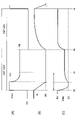
- FIG. 7 schematically shows waveform diagrams of main parts during energization control of the solenoid 51a, and the detection timing of abnormality detection will be described below with reference to the diagram.
- the low-side transistor 53 Since energization control of the solenoid 51a of the purge valve 51 is normally performed by so-called PWM control, the low-side transistor 53 is turned on/off by the microcomputer 54 at a predetermined duty ratio.
- the voltage Vout at the second connection terminal 58b drops to a voltage near zero V, while the energization current Is gradually increases (Fig. 7(A) and FIG. 7(B)).
- the detection voltage Vdet of the resistance detection circuit 55 also rises with the increase in the current Is, and then becomes a constant voltage (see FIG. 7(C)).
- the low-side transistor 53 After a predetermined energization time, the low-side transistor 53 is turned off by the microcomputer 54, but due to the inductance of the solenoid 51a, the voltage Vout at the second connection terminal 58b temporarily rises sharply and reaches the predetermined clamp voltage Vcl. After that, it gradually decreases with the lapse of time to reach a predetermined battery voltage VB (see FIG. 7A). Due to the influence of the inductance, the conducting current Is also does not immediately become zero when the low-side transistor 53 is turned off, but decreases over time (see FIG. 7B).
- the output voltage Vdet of the resistance detection circuit 55 temporarily reaches the maximum output (5 V in this example) due to the influence of the inductance when the low-side transistor 53 is turned off, and then once drops to 0 V as the inductance decreases. After that, the output state returns to the normal state (see FIG. 7(C)).
- the period indicated by Ttr is a period during which the inductance causes a transient response. After this period, the output state of the resistance detection circuit 55 returns to normal.
- the detection of the solenoid resistance value by the resistance detection circuit 55 and the detection of an abnormality such as a short circuit of the battery are performed after the above-described transient response period Ttr has elapsed, that is, after time ta until time tb when the low-side transistor 53 is turned on again. will be limited to between
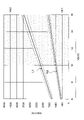
- FIG. 8 shows an example of the change characteristic of the output voltage Vdet of the resistance detection circuit 55 with respect to the change of the battery voltage VB when the solenoid resistance value is 38.5 ⁇ . is indicated by a characteristic line L1"). Dotted lines above and below the characteristic line L1 indicate an example of the variation range. 8 shows an example in which the maximum output voltage of the resistance detection circuit 55 is 5V.
- characteristic line L2 shows an example of the change characteristic of the output voltage Vdet of the resistance detection circuit 55 with respect to the change of the battery voltage VB when the solenoid resistance value is 17 ⁇ . ). Dotted lines above and below the characteristic line L2 indicate an example of the variation range.
- the threshold Vth1 of the first comparator 59 is 500 mV and the threshold Vth2 of the second comparator 60 is 4500 mV. Therefore, in this case, the output voltage Vdet of the resistance detection circuit 55 that can be used for detecting the solenoid resistance value in the microcomputer 54 is limited to the range of 500 mV ⁇ Vdet ⁇ 4500 mV.
- the characteristic lines L1 and L2 described above are the results of adjusting the circuit constants of the resistance detection circuit 55, etc. in consideration of the limited range of the output voltage Vdet.
- the slopes of the characteristic lines L1 and L2 that is, the change in the output voltage Vdet with respect to the change in the battery voltage VB, should be secured as large as possible. Is required.
- the limitation of the output voltage Vdet as described above naturally limits the resolution and accuracy of the solenoid resistance value detection. For example, if the characteristic line L1 shown in FIG. Suppose that the resolution and accuracy of the solenoid resistance value detection can be secured by increasing the size.
- the purge valve drive control device includes: A purge valve drive control device comprising a driver circuit for energizing a solenoid of a solenoid type purge valve, and a microcomputer configured to be able to control the valve opening degree of the solenoid type purge valve via the driver circuit. and One end of the solenoid is applied with a battery voltage through a first connection terminal provided on the verge valve drive control device, and the other end is connected to a second connection terminal provided on the verge valve drive control device.
- a drive transistor as a low-side transistor is connected in series with a shunt resistor between the second connection terminal and the ground in the order of the drive transistor and the shunt resistor from the second connection terminal side. and an overcurrent detection circuit configured to detect generation of overcurrent in the drive transistor based on the voltage of the shunt resistor;
- the microcomputer is configured to determine whether or not a battery short-circuit equivalent to an electrical short-circuit state between the first connection terminal and the second connection terminal has occurred based on the output of the overcurrent detection circuit. It will be.
- a battery short-circuit in which the potential of the connection point between the drive transistor and the solenoid becomes the battery voltage can be detected based on the current flowing through the drive transistor by using the drive transistor.
- it is separate from the solenoid resistance value detection circuit. Resistance value detection can be ensured.
- a comparator is provided to compare the voltage at the connection point between the drive transistor and the solenoid with a reference voltage, thereby preventing a ground short circuit in which the connection point is shorted to the ground, or disconnection between the drive transistor and the solenoid. This makes it possible to detect an open terminal, as in the case of a short circuit in a battery, without degrading the resolution and accuracy of the solenoid resistance value detection. It is something that plays.
- FIG. 1 is a configuration diagram showing a configuration example of a purge valve drive control device according to an embodiment of the present invention
- FIG. 4 is a flowchart showing a battery short-circuit detection procedure by abnormality detection processing in the purge valve drive control device according to the embodiment of the present invention
- 4 is a flow chart showing a ground short circuit/terminal open detection procedure by abnormality detection processing in the purge valve drive control device according to the embodiment of the present invention.
- FIG. 4(A) is a waveform diagram schematically showing signal changes of main parts for explaining the drive state of the purge valve and the timing of abnormality detection by the purge valve drive control device according to the embodiment of the present invention.
- FIG. 4B is a waveform diagram schematically showing changes in the voltage Vout of the connection terminal of , FIG.
- FIG. 4B is a waveform diagram schematically showing changes in the current Is flowing through the second connection terminal, and FIG. 4 is a waveform diagram schematically showing changes in the output voltage Vdet of the resistance detection voltage amplifier;
- FIG. 5 is a schematic diagram illustrating the relationship between on/off of a drive transistor of a valve drive circuit provided in the purge valve drive control device according to the embodiment of the present invention and an abnormality detection operation;
- FIG. 2 is a configuration diagram showing a configuration example of a conventional device;
- FIG. 7A is a waveform diagram schematically showing changes in signals of main parts for explaining the drive state of a verge valve and the timing of abnormality detection by a conventional device, FIG. FIG.
- FIG. 7B is a waveform diagram schematically showing changes in the solenoid current Is
- FIG. 7C is a waveform diagram schematically showing changes in the detection voltage of the resistance detection circuit. It is a waveform diagram shown.
- FIG. 5 is a characteristic diagram showing the correlation between the battery voltage and the output voltage of the resistance value detection circuit in detecting the solenoid resistance value by the conventional device;
- FIG. 1 An embodiment of the present invention will be described below with reference to FIGS. 1 to 5.
- FIG. The members, arrangement, etc., described below do not limit the present invention, and can be modified in various ways within the spirit and scope of the present invention.
- First, an example configuration of a purge valve drive control device according to an embodiment of the present invention will be described with reference to FIG.
- the purge valve drive control device according to the embodiment of the present invention controls the drive of the solenoid purge valve 1 and detects an abnormality ( Details will be described later) is configured to be executed.
- the vehicle electronic control unit 100 includes a microcomputer (denoted as “CPU” in FIG. 1) 110, a driver circuit (denoted as “DRV” in FIG. 1) 120, and a resistance detection voltage Mainly composed of an amplifier 130, a battery voltage detection circuit (denoted as “VB-DET” in FIG. 1) 140, and a voltage dividing resistor (denoted as “Rdiv” in FIG. 1) 2 It has become.
- the microcomputer 110 has storage elements such as RAM and ROM (not shown), an analog/digital converter (not shown), an interface circuit, and the like, and has a well-known configuration.
- the microcomputer 110 according to the embodiment of the present invention is configured to be capable of executing various control processes such as solenoid resistance value detection, purge valve drive control, and abnormality detection, as described later in detail.
- the vehicle electronic control unit 100 is provided with first and second connection terminals 3a and 3b for connection with the purge valve 1 provided outside. That is, the battery voltage VB is applied to the first connection terminal 3a, and one end of the solenoid 1a of the purge valve 1 is connected. The other end of the solenoid 1a is connected to a second connection terminal 3b, and this second connection terminal 3b is connected to the output stage of the driver circuit 120.
- the solenoid 1a is connected to the driver circuit as described later. 120 controls energization.
- the resistance detection voltage amplifier 130 amplifies and outputs a voltage necessary for the microcomputer 110 to calculate the solenoid resistance value, which is the resistance value of the solenoid 1a.
- the resistance detection voltage amplifier 130 has a configuration of a well-known amplifier circuit.
- One input stage of the resistance detection voltage amplifier 130 is connected to the first connection terminal 3a to receive the battery voltage VB.
- the other input stage of the resistance detection voltage amplifier 130 is connected to the second connection terminal 3b, and the voltage dividing resistor 2 is connected between the second connection terminal 3b and the ground.
- a voltage corresponding to the voltage drop across voltage dividing resistor 2 is applied to the other input stage of resistance detection voltage amplifier 130 .
- the voltage at the second connection terminal 3b is the drive output voltage Vout
- the input voltage of the resistance detection voltage amplifier 130 is the differential voltage Vdef
- the amplification degree of the resistance detection voltage amplifier 130 is ⁇
- the battery voltage is VB
- the resistance detection voltage amplifier Assuming that the output voltage of 130 is the detection voltage Vdet, the detection voltage Vdet input to the microcomputer 110 is represented by Equation 1 below.
- Vout is represented by Equation 3 below.
- Vout VB ⁇ Rdiv/(Rva+Rdiv)...Equation 3
- the solenoid resistance value Rva is calculated based on Equation 4 below.
- the solenoid resistance value calculated as described above is used for PWM control of the drive transistor 4 provided in the driver circuit 120, which will be described later, by the microcomputer 110.
- the battery voltage detection circuit 140 is configured to convert the battery voltage VB into a voltage suitable for the microcomputer 110 and output it. In the microcomputer 110, a process of monitoring whether or not the battery voltage VB is normal is executed. Also, the value of the battery voltage VB obtained by the battery voltage detection circuit 140 is used for the above-described calculation of the solenoid resistance value and the like.
- the driver circuit 120 includes a driving transistor 4, a shunt resistor (denoted as “Rs” in FIG. 1) 5, and an overcurrent detection circuit (denoted as “I-DET” in FIG. 1) 11. , a comparator 12 and an error register (denoted as “F-REG” in FIG. 1) 13 as main components.
- the driver circuit 120 according to the embodiment of the present invention controls the energization of the solenoid 1a in the same manner as in the conventional art, and is configured to be capable of detecting an abnormality together with the microcomputer 110, as will be described later in detail.
- abnormality detection means detection of an abnormal state of voltage and current at the first and second connection terminals 3a and 3b.
- the above-described abnormal states in the embodiment of the present invention are broadly classified into “battery short-circuit” and “ground short-circuit/terminal open”.
- Battery short circuit refers to a state equivalent to an electrical short circuit between the first connection terminal 3a and the second connection terminal 3b.
- battery short circuit refers to a state in which the battery voltage VB is directly applied to the second connection terminal 3b.
- ground short-circuit/terminal open is a generic term for ground short-circuit and terminal open. In the embodiment of the present invention, it is not determined whether the ground is short-circuited or the terminal is open, but only whichever is selected (details will be described later).
- Short circuit to ground means a state in which the second connection terminal 3b is connected to the ground
- terminal open means a state in which the connection between the second connection terminal 3b and the solenoid 1a is cut off. It means that the drain of the driving transistor 4 is in an open state.
- the drive transistor 4 is PWM-controlled according to the valve drive control signal Svc input from the microcomputer 110 to control the energization of the solenoid 1a of the purge valve 1.
- FIG. The PWM control of the drive transistor 4 by the microcomputer 110 is basically the same as the conventional one, so it will be briefly described below.
- the duty ratio in the PWM control of the drive transistor 4 is set according to the desired valve opening degree of the purge valve 1, in other words, the operating state of the vehicle, and the drive transistor 4 is driven at that duty ratio. is done.
- PWM control of the driving transistor 4 is executed by feedback control while correcting the duty ratio based on the solenoid resistance value calculated as described above.
- the driving transistor 4 in the embodiment of the present invention functions as a so-called low-side transistor.
- a MOSFET Metal-Oxide-Semiconductor-Field-Effect-Transistor
- the drain of the drive transistor 4 is connected to one end of the solenoid 1a of the verge valve 1 via the second connection terminal 3b.
- a battery voltage VB is applied to the other end of the solenoid 1a through a first connection terminal 3a provided on the vehicle electronic control unit 100. As shown in FIG.
- a shunt resistor 5 is provided between the source of the drive transistor 4 and the ground.
- the valve drive control signal Svc is input to the gate of the drive transistor 4, and under PWM control by the microcomputer 110 as described above, the drive transistor 4 controls the energization current of the solenoid 1a. It has become.
- the overcurrent detection circuit 11 detects an overcurrent flowing through the driving transistor 4 due to the occurrence of a "battery short circuit". That is, first, the voltage of the shunt resistor 5 (hereinafter referred to as "shunt voltage" for convenience of explanation) is input to the input stage of the overcurrent detection circuit 11 .
- shunt voltage the voltage of the shunt resistor 5
- the overcurrent detection circuit 11 is configured to output a predetermined overcurrent detection voltage when the shunt voltage exceeds a predetermined overcurrent reference voltage, assuming that the shunt current Ish has exceeded a predetermined reference overcurrent Ith. It's becoming The overcurrent detection circuit 11 as described above is not unique to the present invention, but has a conventionally well-known circuit configuration.
- the comparator 12 is for detecting the occurrence of a ground short circuit/terminal open circuit.
- the non-inverting input terminal of the comparator 12 is connected to the second connection terminal 3b, while the predetermined judgment reference voltage Vth is applied to the inverting input terminal.
- the driver circuit 120 is operating normally without a "battery short circuit” or a "ground short circuit/terminal open"
- the non-inverting input terminal of the comparator 12 is connected to the drive transistor 4.
- a voltage exceeding a predetermined determination reference voltage Vth corresponding to the operating state is applied. In this case, the comparator 12 outputs a predetermined positive voltage corresponding to the logical value "1".
- a "ground short circuit” in which the second connection terminal 3b is connected to the ground, or a “terminal open” in which the second connection terminal 3b is disconnected from the solenoid 1a and the second connection terminal 3b is open. is generated, the voltage of the non-inverting input terminal of the comparator 12 is in the vicinity of the ground potential in either case, and falls below the reference voltage Vth for judgment.
- the comparator 12 outputs a voltage corresponding to the logic value "0", that is, 0V or a predetermined negative voltage.
- the error register 13 is a register for temporarily storing whether or not a "battery short circuit” has been detected by the overcurrent detection circuit 11 and whether or not a "ground short circuit/terminal open” has been detected by the comparator 12, respectively.
- the error register 13 includes, for example, a register area (hereinafter referred to as a "battery short-circuit register area” for convenience of explanation) for temporarily writing and storing whether or not a "battery short-circuit” has been detected, and a "ground short-circuit/terminal It is divided into register areas (hereinafter referred to as "ground short-circuit/terminal open register areas" for convenience of explanation) for temporarily writing and storing presence/absence of "open” detection (not shown).
- the battery short circuit register area contains a logical value of "1". It is written and stored and held until the output voltage of the overcurrent detection circuit 11 is reset to zero.
- logical value data is a generic term for logical value "1" and logical value "0".
- step S110 If it is determined in step S110 that the driving transistor 4 is in the ON state (YES), battery short-circuit detection will be performed as described below. Further, when it is determined in step S110 that the drive transistor 4 is not in the ON state (in the case of NO), ground short circuit/terminal open detection is performed as will be described later.
- Steps S120 to S150 describe the operation flow of the entire apparatus from the detection of an overcurrent due to a short circuit to the battery by the overcurrent detection circuit 11 until the occurrence of the battery short circuit is determined by the microcomputer 110 . Similarly, steps S120 and steps S160 to S180 are performed until the overcurrent detection circuit 11 detects no overcurrent caused by the battery short circuit and the microcomputer 110 determines that the battery voltage is normal. It describes the flow.
- the overcurrent detection circuit 11 it is determined whether or not there is an "overcurrent occurrence" due to a battery short circuit, ie, "Ish>Ith" (see step S120 in FIG. 2).
- the overcurrent detection circuit 11 when the shunt voltage exceeds a predetermined overcurrent reference voltage, it is determined that an overcurrent has occurred, that is, the shunt current Ish has exceeded a predetermined reference overcurrent Ith (if YES), and the predetermined overcurrent is detected. A detected voltage is output. It should be noted that the overcurrent detection circuit 11 does not operate only at the timing of step S120. It is in a detectable operating state.
- each step in FIG. 2 is for the sake of convenience in explaining the overall flow of abnormality determination processing by the microcomputer 110, the overcurrent detection circuit 11, the comparator 12, and the error register 13. It is not limited.
- "VB short-circuit occurrence error register write” is performed (see step S130 in FIG. 2).
- "VB short circuit occurrence” means the occurrence of a battery short circuit.
- the error register 13 in response to the output of a predetermined overcurrent detection voltage from the overcurrent detection circuit 11, the error register 13 writes a logical value "1" indicating that a battery short circuit has occurred in the above-described battery short circuit register area.
- "error register reading” is performed (see step S140 in FIG. 2). That is, in the microcomputer 110, reading of logical value data from the battery short-circuit register area of the error register 13 is repeatedly performed at predetermined timings.
- the purge valve drive control device when the drive transistor 4 is in the ON state, only the battery short-circuit can be detected as an abnormality.
- the area is only the battery short circuit resistor area.
- step S150 the microcomputer 110 determines that the logic value data read from the battery short-circuit register area of the error register 13 is "1", it is "VB short-circuit occurrence determination", ie, a battery short-circuit occurrence state. (see step S150 in FIG. 2). After the determination in step S150 is made, the process returns to the main routine (not shown), other required processing is executed, and then the above operation is restarted from the beginning.
- alarm processing such as turning on a warning light and sounding an alarm device
- abnormality handling processing such as forcibly stopping device operation, etc. are normally executed.
- the content should be determined individually according to the vehicle specifications, etc., and is not limited to specific processing content.
- the output of the overcurrent detection circuit 11 is a predetermined value corresponding to no battery short circuit.
- a predetermined voltage for example, zero V
- "error register normal write” is performed in the error register 13 (see step S160 in FIG. 2). That is, the logical value "0" is written in the battery short-circuit register area of the error register 13, which corresponds to the normal state in which the battery is not short-circuited.
- step S170 in FIG. 2 the microcomputer 110 reads the logical value data in the battery short-circuit register area of the error register 13 .
- the microcomputer 110 determines that the logic value data read out from the battery short-circuit register area of the error register 13 is a logic value of "0”, it makes a "VB normal determination", that is, a battery short-circuit has occurred. Therefore, it is determined to be in a normal state (see step S180 in FIG. 2). After that, the process returns to the main routine (not shown), and after other required processing is executed, the above-described operations centering on the microcomputer 110 are restarted from the beginning.
- step S110 in FIG. 2 determines whether or not the "driving transistor is ON" (see step S110 in FIG. 2), if it is determined that the driving transistor 4 is not ON (in the case of NO), comparison is made as described below.
- the microcomputer 1102 based on the operations of the unit 12 and the error register 13 executes ground short circuit/terminal open detection. Specifically, the comparator 12 first determines whether or not "terminal voltage detection” is performed, that is, determines whether or not "Vout>Vth” (see step S200 in FIG. 3). ).
- the second connection terminal 3b is connected to the non-inverting input terminal of the comparator 12 as described above, and the output voltage Vout at the second connection terminal 3b is applied to the non-inverting input terminal. A comparison with the determination reference voltage Vth is performed. Since Vout>Vth when no short-circuit to ground or open terminal occurs, the comparator 12 outputs a predetermined voltage (for example, 5 V) corresponding to the logic value High (YES in FIG. 3). case).
- a predetermined voltage for example, 5 V
- the comparator 12 does not operate only at the timing of step S200. It is what it is.
- step S220 in FIG. 3 the logic value data in the ground short/terminal open register area of the error register 13 is read.
- the microcomputer 110 reads the logic value "0" as the logic value data from the ground short/terminal open register area of the error register 13 .
- terminal normality judgment that is, the first and second connection terminals 3a and 3b are electrically is determined to be in a normal state (see step S230 in FIG. 3). After that, the process returns to the main routine (not shown), other required processing is executed, and then the above-described operations centering on the microcomputer 110 are repeated again.
- Vout>Vth if the output voltage Vout is lower than the determination reference voltage Vth (NO in step S200 in FIG. 3), the comparator 12 outputs the logic value "0" as described above. Outputs a predetermined voltage corresponding to When a predetermined voltage corresponding to the logical value "0" is output from the comparator 12, the error register 13 performs "ground short/open error register write" (see step S240 in FIG. 3). . That is, in the error register 13, a logic value "1" is written in the above-described ground short circuit/terminal open register area to indicate that a ground short circuit/terminal open has occurred.
- step S260 in FIG. 3 the process returns to the main routine (not shown), other required processing is executed, and then the above-described operations centering on the microcomputer 110 are repeated again.
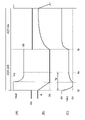
- FIG. 4 shows a waveform diagram schematically showing waveforms of main parts for explaining the temporal relationship between the ON/OFF of the driving transistor 4 and the above-described abnormality detection process.
- the horizontal axis is the time axis. 4A, the vertical axis indicates voltage, the vertical axis indicates current in FIG. 4B, and the vertical axis indicates voltage in FIG. 4C.
- the period from time t0 to time tb is the period in which the driving transistor 4 is off
- the period from time tb to time tc is the period in which the driving transistor 4 is on. Since control of energization to the solenoid 1a by the drive transistor 4 is the same as in the conventional art, an example of change in the output voltage Vout at the second connection terminal 3b accompanying turning on/off of the drive transistor 4 shown in FIG. 4(B) shows an example of a change in the current Is flowing through the solenoid 1a via the second connection terminal 3b, and a change in the output voltage Vdet of the resistance detection voltage amplifier 130 shown in FIG. 4(C). All examples are conventional.
- this is the period in which a transient response due to inductance occurs after the drive transistor 4 is turned off. It was possible to detect a battery short circuit, a ground short circuit, and an open terminal only during the period from time t0 to time ta until the drive transistor 4 was turned on, that is, only from time ta to time tb.
- the comparator 12 is not limited to a specific timing. It is possible to detect a short circuit/open terminal (see steps S200 to S260 in FIG. 3). Also, while the drive transistor 4 is in the ON state, that is, between time tb and time tc, battery short-circuit detection by the resistance detection voltage amplifier 130 is possible without being limited to a specific timing (see FIG. 2). See steps S110 to S180).
- FIG. 5 shows an explanatory diagram for comprehensively explaining the relationship between the ON/OFF state of the driving transistor 4 and the detection of an abnormality.
- ECU terminal state in the upper left column of the paper means the electrical state of the first and second connection terminals 3a and 3b of the vehicle electronic control unit 100.
- Normal "VB short circuit”, “ground short circuit”, and “terminal open” are shown in columns, respectively.
- normal means a state in which no battery short-circuit (VB short-circuit), ground short-circuit or terminal open has occurred, and energization control of the solenoid 1a by the drive transistor 4 is normally performed.
- VB short circuit means a state in which a battery short circuit occurs
- ground short circuit means a state in which the second connection terminal 3b is connected to the ground
- terminal open means the second connection. Each means a state in which the connection between the terminal 3b and the solenoid 1a is cut off.
- the comparison operation using the comparator 12 is used to distinguish between the "ground short circuit” and the "terminal open circuit". However, they are described separately here for the purpose of explaining that the circuit operation is the same.
- the column labeled "FET voltage state” on the right side of “ECU terminal state” indicates the number of values corresponding to the ON/OFF state of the driving transistor 4 for each section of the "ECU terminal state" in the left column. 2 are shown respectively.
- the microcomputer 110 does not determine whether or not the ground short circuit/terminal open occurs, as described above.
- the voltage at the second connection terminal 3b becomes the battery voltage VB (see FIG. 4A).
- the voltage at the second connection terminal 3b becomes the battery voltage VB.
- the microcomputer 110 detects battery short circuit/terminal open based on the output of the comparator 12 (see step S200 and steps S240 to S260 in FIG. 3).
- the comparator 12 provided in the driver circuit 120 can detect ground short-circuit/terminal open.
- the overcurrent detection operation using the drive transistor 4 makes it possible to detect a battery short-circuit. Therefore, it is possible to detect an abnormality at an earlier stage than in the conventional art.
- the configuration can be simplified.
- the output voltage of the resistance detection voltage amplifier 130 is not used for detecting the presence or absence of an abnormality in the first and second connection terminals 3a and 3b, but is used only for detecting the solenoid resistance value. Therefore, higher resolution and accuracy of solenoid resistance value detection are ensured than in the conventional art.
Landscapes
- Engineering & Computer Science (AREA)
- Physics & Mathematics (AREA)
- Electromagnetism (AREA)
- Chemical & Material Sciences (AREA)
- Combustion & Propulsion (AREA)
- Mechanical Engineering (AREA)
- General Engineering & Computer Science (AREA)
- Power Engineering (AREA)
- Testing Of Short-Circuits, Discontinuities, Leakage, Or Incorrect Line Connections (AREA)
Abstract
Description
例えば、キャニスタ内に収納された活性炭に燃料蒸発ガスを吸着させると共に、エンジン稼働時にエンジンの吸入空気の一部をキャニスタに通過させ、パージバルブを介してエンジンの吸気系に放出(パージ)、すなわち、エンジンの吸入口へ流入せしめてエンジンの燃料に供するようにした構成などが、比較的良く知られている。
そのため、パージバルブは、通常、フィードバック制御等でその開度制御が行われる。
特に、ソレノイド式のパージバルブの場合、その開度は通電電流の大きさで決定されるが、通電電流を決定する主要因であるバッテリ電圧とソレノイドの抵抗値が、車両の動作状態や周囲の温度に依存して変化する。
図6には、従来のパージバルブ駆動制御装置の構成例が示されており、以下、同図を参照しつつ従来装置における異常検出について説明する。
この車両用電子制御ユニットECUを用いた従来のパージバルブ駆動制御装置においては、パージバルブ51のソレノイド51a一端にはバッテリ電圧VBが印加される一方、ソレノイド51aの他端は、いわゆるローサイドトランジスタ53により構成されたドライバ回路52に接続されている。
抵抗検出回路55は、バッテリ電圧VBと、分圧抵抗器56に得られる分圧電圧Vdivとの差である差電圧Vdefを増幅出力して検出電圧Vdetとしてマイクロコンピュータ54へ出力するものとなっている。
そして、算出されたソレノイド抵抗値はPWM制御におけるデューティ補正に供されるものとなっている。
すなわち、抵抗検出回路55の出力電圧を、第1及び第2の比較器59,60において、それぞれの閾値Vth1,Vth2と比較し、その比較結果によってマイクロコンピュータ54において異常の有無が判定されるようになっている。
この場合、第1の比較器59において、抵抗検出回路55の出力電圧が第1の閾値Vth1を下回り、その結果、マイクロコンピュータ54においてバッテリ短絡発生と判定される。
まず、図7には、ソレノイド51aの通電制御の際の主要部の波形図が模式的に示されており、以下、同図を参照しつつ、異常検出の検出タイミングについて説明する。
ソレノイド51aの通電に際して、ローサイドトランジスタ53がオンとされると、第2の接続端子58bにおける電圧Voutは、零V近傍の電圧に降下する一方、通電電流Isは、徐々に増大してゆく(図7(A)及び図7(B)参照)。
また、抵抗検出回路55の検出電圧Vdetも通電電流Isの増加に伴い上昇し、その後、一定の電圧となる(図7(C)参照)。
通電電流Isもインダクタンスの影響で、ローサイドトランジスタ53のオフ時に直ぐさま零とはならず、時間経過と共に減少してゆく(図7(B)参照)。
図8には、ソレノイド抵抗値が38.5Ωの場合におけるバッテリ電圧VBの変化に対する抵抗検出回路55の出力電圧Vdetの変化特性例が符号L1を付した実線の特性線(以下、説明の便宜上「特性線L1」と称する)により示されている。なお、特性線L1の上下の点線は変動範囲の例を示している。なお、図8は、抵抗検出回路55の最大出力電圧が5Vの場合の例である。
なお、特性線L2の上下の点線は変動範囲の例を示している。
したがって、この場合、マイクロコンピュータ54におけるソレノイド抵抗値の検出に用いることのできる抵抗検出回路55の出力電圧Vdetは、500mV<Vdet<4500mVの範囲に制限されることとなる。
ソレノイド抵抗値検出において、より高い分解能、精度を確保するためには、例えば、特性線L1,L2の傾き、すなわち、バッテリ電圧VBの変化に対する出力電圧Vdetの変化を可能な範囲で大きく確保することが必要となる。
例えば、仮に、図8に示された特性線L1を、その上端側、すなわち、バッテリ電圧VB=16V付近の出力電圧Vdetが5V近傍となるように回路定数等を調整し、特性線の傾きを大きくしてソレノイド抵抗値検出の分解能、精度をより高く確保できるようにしたとする。
ソレノイド式パージバルブのソレノイドへの通電を行うドライバ回路が設けられると共に、前記ドライバ回路を介して前記ソレノイド式パージバルブの弁開度を制御可能に構成されてなるマイクロコンピュータを有してなるパージバルブ駆動制御装置であって、
前記ソレノイドは、一端が前記バージバルブ駆動制御装置に設けられた第1の接続端子を介してバッテリ電圧が印加される一方、他端が前記バージバルブ駆動制御装置に設けられた第2の接続端子に接続され、
前記ドライバ回路は、ローサイドトランジスタとしての駆動トランジスタがシャント抵抗器と共に、前記第2の接続端子とグランドとの間に、前記第2の接続端子側から前記駆動トランジスタ、シャント抵抗器の順に直列接続されて設けられてなり、
前記シャント抵抗器の電圧を基に前記駆動トランジスタにおける過電流の発生を検出可能に構成されてなる過電流検出回路が設けられ、
前記マイクロコンピュータは、前記過電流検出回路の出力に基づいて、前記第1の接続端子と前記第2の接続端子の電気的短絡状態に等価なバッテリ短絡の発生の有無を判定可能に構成されてなるものである。
さらに、比較器を設け、駆動トランジスタとソレノイドの接続点の電圧を基準電圧と比較することで、その接続点がグランドと短絡状態となるグランド短絡、又は、駆動トランジスタとソレノイドとの接続が断たれた端子開放の検出が可能となり、バッテリ短絡同様、ソレノイド抵抗値検出の分解能、精度を劣化させることがなく、安定したソレノイド抵抗値検出を確保しつつ、回路の異常を検出することができるという効果を奏するものである。
なお、以下に説明する部材、配置等は本発明を限定するものではなく、本発明の趣旨の範囲内で種々改変することができるものである。
最初に、本発明の実施の形態におけるパージバルブ駆動制御装置の構成例について、図1を参照しつつ説明する。
本発明の実施の形態におけるパージバルブ駆動制御装置は、車両に搭載された車両用電子制御ユニット(図1においては「ECU」と表記)100を中心に、ソレノイド式パージバルブ1の駆動制御と共に異常検出(詳細は後述)が実行されるよう構成されたものとなっている。
本発明の実施の形態におけるマイクロコンピュータ110は、詳細は後述するようにソレノイド抵抗値検出、パージバルブ駆動制御、異常検出等の各種の制御処理が実行可能に構成されている。
すなわち、第1の接続端子3aには、バッテリ電圧VBが印加されると共に、パージバルブ1のソレノイド1aの一端が接続されている。
そして、ソレノイド1aの他端は、第2の接続端子3bに接続され、この第2の接続端子3bは、ドライバ回路120の出力段に接続されており、ソレノイド1aは、後述するようにドライバ回路120により通電制御されるようになっている。
また、抵抗検出電圧増幅器130の他方の入力段は、第2の接続端子3bに接続されており、この第2の接続端子3bとグランドとの間には、分圧抵抗器2が接続されている。
ここで、第2の接続端子3bにおける電圧を駆動出力電圧Vout、抵抗検出電圧増幅器130の入力電圧を差分電圧Vdef、抵抗検出電圧増幅器130の増幅度をα、バッテリ電圧をVB、抵抗検出電圧増幅器130の出力電圧を検出電圧Vdetとすると、マイクロコンピュータ110に入力される検出電圧Vdetは、下記する式1で表される。
マイクロコンピュータ110においては、バッテリ電圧VBが正常か否かの監視処理が実行されるようになっている。また、バッテリ電圧検出回路140により得られたバッテリ電圧VBの値は、上述のソレノイド抵抗値の算出等に供されるようになっている。
本発明の実施の形態におけるドライバ回路120は、従来同様のソレノイド1aの通電制御を行うと共に、詳細は後述するように、マイクロコンピュータ110と共に異常検出が可能に構成されている。
本発明の実施の形態における上述の異常状態は、具体的には、以下に説明するように、「バッテリ短絡」と「グランド短絡・端子開放」の2つに大別される。
「バッテリ短絡」は、第1の接続端子3aと第2の接続端子3bとが電気的に短絡されたと等価な状態をいう。すなわち、「バッテリ短絡」は、換言すれば、バッテリ電圧VBが第2の接続端子3bに直接印加された状態を言う。
なお、「グランド短絡」は、第2の接続端子3bがグランドと接続された状態を、「端子開放」は、第2の接続端子3bとソレノイド1aの接続が断たれた状態、すなわち、後述する駆動トランジスタ4のドレインが開放状態をいう。
最初に、駆動トランジスタ4は、マイクロコンピュータ110から入力されるバルブ駆動制御信号Svcに応じてPWM制御されて、パージバルブ1のソレノイド1aの通電を制御するものとなっている。
マイクロコンピュータ110による駆動トランジスタ4のPWM制御は、基本的に従来同様のものであるので、以下に概略的に説明することとする。
具体的には、本発明の実施の形態において、駆動トランジスタ4には、MOSFET(Metal-Oxide-Semiconductor-Field-Effect-Transistor)が用いられている。駆動トランジスタ4のドレインは、第2の接続端子3bを介して、バージバルブ1のソレノイド1aの一端に接続されている。
ソレノイド1aの他端は、車両用電子制御ユニット100に設けられた第1の接続端子3aを介してバッテリ電圧VBが印加されるようになっている。
駆動トランジスタ4のゲートには、上述したバルブ駆動制御信号Svcが入力されて、先に述べたようにマイクロコンピュータ110によるPWM制御を受けて、駆動トランジスタ4によるソレノイド1aの通電電流制御が行われるようになっている。
すなわち、まず、過電流検出回路11の入力段には、シャント抵抗器5の電圧(以下、説明の便宜上「シャント電圧」と称する)が入力されるようになっている。
比較器12の非反転入力端子は、第2の接続端子3bに接続される一方、反転入力端子には、所定の判定基準電圧Vthが印加されている。
”バッテリ短絡”や”グランド短絡・端子開放”が発生しておらず、ドライバ回路120が正常に動作している状態にあっては、比較器12の非反転入力端子には、駆動トランジスタ4の動作状態に応じた所定の判定用基準電圧Vthを越える電圧が印加される。
この場合、比較器12は、論理値”1”に相当する所定の正電圧を出力するようになっている。
その結果、比較器12は、論理値”0”に相当する電圧、すなわち、0V、又は、所定の負電圧を出力するものとなっている。
かかるエラーレジスタ13は、たとえば、”バッテリ短絡”の検出の有無を一時的に書込、記憶するためのレジスタ領域(以下、説明の便宜上「バッテリ短絡レジスタ領域」称する)と、”グランド短絡・端子開放”の検出の有無を一時的に書込、記憶するためのレジスタ領域(以下、説明の便宜上「グランド短絡・端子開放レジスタ領域」称する)に、それぞれ区分されている(図示せず)。
なお、ここで、”論理値データ”は、論理値”1”と論理値”0”の総称である。
まず、マイクロコンピュータ110による処理が開始されると、”駆動トランジスタON”か否かの判定、すなわち、駆動トランジスタ4がオン状態(駆動状態)か否かが判定される(図2のステップS110参照)。
また、ステップS120、ステップS160乃至ステップS180は、同様に、過電流検出回路11によってバッテリ短絡による過電流の検出がなく、マイクロコンピュータ110によってバッテリ電圧正常と判定されるまでの本装置全体の動作の流れを説明したものである。
なお、過電流検出回路11は、ステップS120のタイミングでのみ動作するものではなく、パージバルブ駆動制御装置の起動に伴い電源電圧の供給が開始された以降は、常時、上述の過電流発生の有無を検出可能な動作状態にある。
しかして、過電流検出回路11から所定の過電流検出電圧が出力されることで、”VB短絡発生エラーレジスタ書込”が行われる(図2のステップS130参照)。ここで、”VB短絡発生”は、バッテリ短絡の発生を意味する。
一方、マイクロコンピュータ110においては、”エラーレジスタ読出”が行われる(図2のステップS140参照)。
すなわち、マイクロコンピュータ110においては、エラーレジスタ13のバッテリ短絡レジスタ領域の論理値データの読み出しが、予め定められたタイミングで繰り返し行われる。
これによって、エラーレジスタ13において、”エラーレジスタ正常書込”が行われる(図2のステップS160参照)。
すなわち、エラーレジスタ13のバッテリ短絡レジスタ領域には、バッテリ短絡が生じていない正常状態であることに対応する論理値”0”が書き込まれることとなる。
すなわち、マイクロコンピュータ110は、エラーレジスタ13のバッテリ短絡レジスタ領域の論理値データの読み出しを行う。
この後、図示されないメインルーチンへ戻り、他の所要の処理が実行された後、マイクロコンピュータ110を中心とした上述の動作が最初から再度開始されることとなる。
以下、具体的に説明すれば、先ず、比較器12においては、”端子電圧検出”か否かの判定、すなわち、”Vout>Vth”か否かの判定が行われる(図3のステップS200参照)。
グランド短絡・端子開放が発生していな状態においては、Vout>Vthとなるため、比較器12は論理値Highに相当する所定の電圧(例えば、5V)の出力状態となる(図3のYESの場合)。
すなわち、エラーレジスタ13のグランド短絡・端子開放レジスタ領域に、第2の接続端子3bにおける出力電圧Voutが正常であることに対応する論理値”0”が書き込まれることとなる。
すなわち、マイクロコンピュータ110においては、エラーレジスタ13のグランド短絡・端子開放レジスタ領域の論理値データの読み出しが行われる。
マイクロコンピュータ110は、エラーレジスタ13のグランド短絡・端子開放レジスタ領域から論理値データとして論理値”0”を読み出すこととなる。
この後、図示されないメインルーチンへ戻り、他の所要の処理が実行された後、マイクロコンピュータ110を中心とした上述の動作が再度繰り返されることとなる。
比較器12から論理値”0”に相当する所定の電圧が出力されると、エラーレジスタ13において、”グランド短絡・開放エラーレジスタ書込”が行われることとなる(図3のステップS240参照)。
すなわち、エラーレジスタ13において、先に述べたグランド短絡・端子開放レジスタ領域に、グランド短絡・端子開放が発生したとする論理値”1”が書き込まれることとなる。
すなわち、マイクロコンピュータ110においては、エラーレジスタ13のグランド短絡・端子開放レジスタ領域から論理値”1”の論理値データの読み出しが行われる。
この後、図示されないメインルーチンへ戻り、他の所要の処理が実行された後、マイクロコンピュータ110を中心とした上述の動作が再度繰り返されることとなる。
図4(A)乃至図4(C)において、横軸はいずれも時間軸である。
また、図4(A)において縦軸は電圧を、図4(B)において縦軸は電流を、図4(C)において縦軸は電圧を、それぞれ示している。
駆動トランジスタ4によるソレノイド1aへの通電制御は従来同様であるので、図4(A)に示された駆動トランジスタ4のオン・オフに伴う第2の接続端子3bにおける出力電圧Voutの変化例、図4(B)に示された第2の接続端子3bを介してソレノイド1aに流れる通電電流Isの変化例、及び、図4(C)に示された抵抗検出電圧増幅器130の出力電圧Vdetの変化例は、いずれも従来と同様である。
また、駆動トランジスタ4がオン状態の間、すなわち、時刻tb~時刻tcまでの間であれば、特定のタイミングに限定されずに抵抗検出電圧増幅器130によるバッテリ短絡検出が可能である(図2のステップS110乃至ステップS180参照)。
図5に示された説明図において、紙面左側上部の欄の”ECU端子状態”は、車両用電子制御ユニット100の第1及び第2の接続端子3a,3bにおける電気的状態を意味し、その列には、”正常”、”VB短絡”、”グランド短絡”、”端子開放”が、それぞれ区分されて示されている。
また、”VB短絡”は、バッテリ短絡が発生している状態を、”グランド短絡”は、第2の接続端子3bがグランドと接続状態となる状態を、”端子開放”は、第2の接続端子3bとソレノイド1aとの接続が断たれた状態を、それぞれ意味する。
まず、ECU端子状態が正常状態にあって、駆動トランジスタ4がオンの場合、第2の接続端子3bにおける電圧は零Vとなる(図4(A)参照)。
次に、ECU端子状態がVB短絡(バッテリ短絡)であって、駆動トランジスタ4がオンの場合、シャント抵抗器5に過電流が流れることとなる。この場合、過電流検出に基づいてマイクロコンピュータ110によりバッテリ短絡が検出されることとなる(図2のステップS110乃至ステップS150参照)。
この場合、駆動トランジスタ4の動作が正常状態にある場合と区別できないため、マイクロコンピュータ110によるグランド短絡・端子開放の発生か否かの判定は行われないことは先に述べた通りである。
次に、ECU端子状態がバッテリ短絡であって、駆動トランジスタ4オフの場合、第2の接続端子3bにおける電圧は、バッテリ電圧VBとなる。
しかも、駆動トランジスタ4を流用することができるので、構成の簡素化が図られる。
またさらに、抵抗検出電圧増幅器130は、従来と異なり、その出力電圧は、第1及び第2の接続端子3a,3bにおける異常の有無の検出に用いることなく、ソレノイド抵抗値の検出にのみ供されるため、従来に比して、より高いソレノイド抵抗値検出の分解能、精度が確保されることとなる。
Claims (3)
- ソレノイド式パージバルブのソレノイドへの通電を行うドライバ回路が設けられると共に、前記ドライバ回路を介して前記ソレノイド式パージバルブの弁開度を制御可能に構成されてなるマイクロコンピュータを有してなるパージバルブ駆動制御装置であって、
前記ソレノイドは、一端が前記バージバルブ駆動制御装置に設けられた第1の接続端子を介してバッテリ電圧が印加される一方、他端が前記バージバルブ駆動制御装置に設けられた第2の接続端子に接続され、
前記ドライバ回路は、ローサイドトランジスタとしての駆動トランジスタがシャント抵抗器と共に、前記第2の接続端子とグランドとの間に、前記第2の接続端子側から前記駆動トランジスタ、シャント抵抗器の順に直列接続されて設けられてなり、
前記シャント抵抗器の電圧を基に前記駆動トランジスタにおける過電流の発生を検出可能に構成されてなる過電流検出回路が設けられ、
前記マイクロコンピュータは、前記過電流検出回路の出力に基づいて、前記第1の接続端子と前記第2の接続端子の電気的短絡状態に等価なバッテリ短絡の発生の有無を判定可能に構成されてなること特徴とするパージバルブ駆動制御装置。 - 前記ドライバ回路には、前記第2の接続端子の電圧と判定基準電圧との比較に基づいて、前記第2の接続端子がグランドと短絡された状態に等価なグランド短絡、又は、前記第2の接続端子と前記ソレノイドとの接続が断たれた端子開放の発生を検出可能とする比較器が設けられ、
前記マイクロコンピュータは、前記比較器の出力に基づいて、グランド短絡か端子開放のいずれかであるグランド短絡・端子開放の発生の有無を判定可能に構成されてなることを特徴とする請求項2記載のパージバルブ駆動制御装置。 - 前記ドライバ回路には、前記過電流検出回路による過電流検出の有無に応じた所定の論理値データ、及び、前記比較器によるグランド短絡、又は、端子開放の検出の有無に応じた所定の論理値データを、それぞれ別個に書込、蓄積可能に構成されたエラーレジスタが設けられ、
前記マイクロコンピュータは、前記エラーレジスタに前記論理値データに基づいて、バッテリ短絡、グランド短絡・端子開放の発生の有無を判定可能に構成されてなることを特徴とする請求項2記載のパージバルブ駆動制御装置。
Priority Applications (2)
| Application Number | Priority Date | Filing Date | Title |
|---|---|---|---|
| US18/560,622 US12322544B2 (en) | 2021-05-11 | 2022-03-11 | Purge valve driving control device |
| JP2023520858A JP7662772B2 (ja) | 2021-05-11 | 2022-03-11 | パージバルブ駆動制御装置 |
Applications Claiming Priority (2)
| Application Number | Priority Date | Filing Date | Title |
|---|---|---|---|
| JP2021-080337 | 2021-05-11 | ||
| JP2021080337 | 2021-05-11 |
Publications (1)
| Publication Number | Publication Date |
|---|---|
| WO2022239446A1 true WO2022239446A1 (ja) | 2022-11-17 |
Family
ID=84028150
Family Applications (1)
| Application Number | Title | Priority Date | Filing Date |
|---|---|---|---|
| PCT/JP2022/010978 Ceased WO2022239446A1 (ja) | 2021-05-11 | 2022-03-11 | パージバルブ駆動制御装置 |
Country Status (3)
| Country | Link |
|---|---|
| US (1) | US12322544B2 (ja) |
| JP (1) | JP7662772B2 (ja) |
| WO (1) | WO2022239446A1 (ja) |
Citations (8)
| Publication number | Priority date | Publication date | Assignee | Title |
|---|---|---|---|---|
| JPH0784655A (ja) * | 1993-09-16 | 1995-03-31 | Nippondenso Co Ltd | 駆動回路 |
| JPH07293732A (ja) * | 1994-04-19 | 1995-11-10 | Unisia Jecs Corp | 電磁アクチュエータ駆動装置 |
| JP2007010563A (ja) * | 2005-07-01 | 2007-01-18 | Denso Corp | 誘導性負荷の異常検出装置 |
| JP2008182874A (ja) * | 2006-12-25 | 2008-08-07 | Denso Corp | 負荷駆動装置 |
| JP2017008888A (ja) * | 2015-06-25 | 2017-01-12 | 本田技研工業株式会社 | 内燃機関の制御装置 |
| WO2018047553A1 (ja) * | 2016-09-12 | 2018-03-15 | ボッシュ株式会社 | 制御装置 |
| WO2018198631A1 (ja) * | 2017-04-25 | 2018-11-01 | 日立オートモティブシステムズ株式会社 | 電子制御装置 |
| KR101957485B1 (ko) * | 2017-11-02 | 2019-03-12 | 현대오트론 주식회사 | 로우 사이드 구동 ic 고장진단 장치 및 방법 |
Family Cites Families (15)
| Publication number | Priority date | Publication date | Assignee | Title |
|---|---|---|---|---|
| US5653885A (en) * | 1990-07-13 | 1997-08-05 | Isco, Inc. | Apparatus and method for supercritical fluid extraction |
| US5173188A (en) * | 1990-07-13 | 1992-12-22 | Isco, Inc. | Apparatus and method for supercritical fluid extraction |
| US5250195A (en) * | 1990-07-13 | 1993-10-05 | Isco, Inc. | Apparatus and method for supercritical fluid extraction |
| US5268102A (en) * | 1990-07-13 | 1993-12-07 | Isco, Inc. | Apparatus and method for supercritical fluid extraction |
| US5268103A (en) * | 1990-07-13 | 1993-12-07 | Isco, Inc. | Apparatus and method for supercritical fluid extraction |
| US5635070A (en) * | 1990-07-13 | 1997-06-03 | Isco, Inc. | Apparatus and method for supercritical fluid extraction |
| US5690828A (en) * | 1990-07-13 | 1997-11-25 | Isco, Inc. | Apparatus and method for supercritical fluid extraction |
| JP3681041B2 (ja) * | 1999-02-16 | 2005-08-10 | 三菱電機株式会社 | 筒内噴射式内燃機関の制御装置 |
| JP4099092B2 (ja) * | 2002-03-26 | 2008-06-11 | 東京エレクトロン株式会社 | 基板処理装置および基板処理方法、高速ロータリバルブ |
| WO2006028215A1 (ja) * | 2004-09-09 | 2006-03-16 | Tokyo Electron Limited | 薄膜キャパシタ及びその形成方法、及びコンピュータ読み取り可能な記憶媒体 |
| KR100800377B1 (ko) * | 2006-09-07 | 2008-02-01 | 삼성전자주식회사 | 화학기상증착설비 |
| US8129289B2 (en) * | 2006-10-05 | 2012-03-06 | Micron Technology, Inc. | Method to deposit conformal low temperature SiO2 |
| JP2013199874A (ja) | 2012-03-26 | 2013-10-03 | Hitachi Automotive Systems Ltd | 負荷駆動装置 |
| CN104520975B (zh) * | 2012-07-30 | 2018-07-31 | 株式会社日立国际电气 | 衬底处理装置及半导体器件的制造方法 |
| JPWO2015060069A1 (ja) * | 2013-10-22 | 2017-03-09 | 株式会社日立国際電気 | 微細パターンの形成方法、半導体装置の製造方法、及び基板処理装置並びに記録媒体 |
-
2022
- 2022-03-11 US US18/560,622 patent/US12322544B2/en active Active
- 2022-03-11 WO PCT/JP2022/010978 patent/WO2022239446A1/ja not_active Ceased
- 2022-03-11 JP JP2023520858A patent/JP7662772B2/ja active Active
Patent Citations (8)
| Publication number | Priority date | Publication date | Assignee | Title |
|---|---|---|---|---|
| JPH0784655A (ja) * | 1993-09-16 | 1995-03-31 | Nippondenso Co Ltd | 駆動回路 |
| JPH07293732A (ja) * | 1994-04-19 | 1995-11-10 | Unisia Jecs Corp | 電磁アクチュエータ駆動装置 |
| JP2007010563A (ja) * | 2005-07-01 | 2007-01-18 | Denso Corp | 誘導性負荷の異常検出装置 |
| JP2008182874A (ja) * | 2006-12-25 | 2008-08-07 | Denso Corp | 負荷駆動装置 |
| JP2017008888A (ja) * | 2015-06-25 | 2017-01-12 | 本田技研工業株式会社 | 内燃機関の制御装置 |
| WO2018047553A1 (ja) * | 2016-09-12 | 2018-03-15 | ボッシュ株式会社 | 制御装置 |
| WO2018198631A1 (ja) * | 2017-04-25 | 2018-11-01 | 日立オートモティブシステムズ株式会社 | 電子制御装置 |
| KR101957485B1 (ko) * | 2017-11-02 | 2019-03-12 | 현대오트론 주식회사 | 로우 사이드 구동 ic 고장진단 장치 및 방법 |
Also Published As
| Publication number | Publication date |
|---|---|
| JPWO2022239446A1 (ja) | 2022-11-17 |
| JP7662772B2 (ja) | 2025-04-15 |
| US12322544B2 (en) | 2025-06-03 |
| US20240258005A1 (en) | 2024-08-01 |
Similar Documents
| Publication | Publication Date | Title |
|---|---|---|
| CN100587247C (zh) | 发动机控制装置 | |
| US9162639B2 (en) | In-vehicle electronic control unit and power feeding control method of the same | |
| KR101619597B1 (ko) | 후방 산소센서의 고장 검출 방법 | |
| JP2004347423A (ja) | 電気負荷の異常検出装置及び電子制御装置 | |
| US11708801B2 (en) | Load drive device, engine system | |
| CN103036494A (zh) | 双极电机控制器中的过流条件的诊断 | |
| JP4415779B2 (ja) | 二次空気導入システム用駆動装置 | |
| US20090109588A1 (en) | Load driver with wire break detection circuit | |
| JP3988609B2 (ja) | 酸素センサの異常検出装置 | |
| JP4736569B2 (ja) | 誘導性負荷の異常検出装置 | |
| EP1473611B1 (en) | Load failure diagnosis method and apparatus and load failure processing method and apparatus | |
| CN118375536A (zh) | 一种开关阀虚接故障诊断方法、装置、设备以及汽车 | |
| US6154351A (en) | Apparatus for detecting abnormality in direct current motor driving system | |
| WO2022239446A1 (ja) | パージバルブ駆動制御装置 | |
| WO2014103554A1 (ja) | グロープラグ診断方法及び車両用グロープラグ駆動制御装置 | |
| JP2009031153A (ja) | 酸素センサの制御装置 | |
| JP3916867B2 (ja) | 車載電気負荷駆動系の異常検出装置 | |
| CN102341584A (zh) | 识别电引线中的中断的方法和设备 | |
| JP4877291B2 (ja) | ヒータ劣化検出装置 | |
| JP7055873B2 (ja) | 車載電子制御装置 | |
| CN116927966A (zh) | 发动机可变气门正时机构的响应性故障诊断方法及装置 | |
| JPH02165069A (ja) | 電気回路の異常検出装置 | |
| US20150153751A1 (en) | Power supply circuit and electronic control unit employing the same | |
| JPWO2020110821A1 (ja) | 負荷駆動装置および燃料噴射装置の制御方法 | |
| KR101448526B1 (ko) | 자동차의 자동 온도 조절기용 배터리 탈장착 감지 제어 장치 |
Legal Events
| Date | Code | Title | Description |
|---|---|---|---|
| 121 | Ep: the epo has been informed by wipo that ep was designated in this application |
Ref document number: 22807153 Country of ref document: EP Kind code of ref document: A1 |
|
| WWE | Wipo information: entry into national phase |
Ref document number: 2023520858 Country of ref document: JP |
|
| WWE | Wipo information: entry into national phase |
Ref document number: 18560622 Country of ref document: US |
|
| NENP | Non-entry into the national phase |
Ref country code: DE |
|
| 122 | Ep: pct application non-entry in european phase |
Ref document number: 22807153 Country of ref document: EP Kind code of ref document: A1 |
|
| WWG | Wipo information: grant in national office |
Ref document number: 18560622 Country of ref document: US |