WO2022210585A1 - 透明導電フィルム及び透明導電パターンの形成方法 - Google Patents
透明導電フィルム及び透明導電パターンの形成方法 Download PDFInfo
- Publication number
- WO2022210585A1 WO2022210585A1 PCT/JP2022/015137 JP2022015137W WO2022210585A1 WO 2022210585 A1 WO2022210585 A1 WO 2022210585A1 JP 2022015137 W JP2022015137 W JP 2022015137W WO 2022210585 A1 WO2022210585 A1 WO 2022210585A1
- Authority
- WO
- WIPO (PCT)
- Prior art keywords
- film
- transparent conductive
- resin
- conductive film
- ultraviolet absorber
- Prior art date
- Legal status (The legal status is an assumption and is not a legal conclusion. Google has not performed a legal analysis and makes no representation as to the accuracy of the status listed.)
- Ceased
Links
Images




Classifications
-
- H—ELECTRICITY
- H01—ELECTRIC ELEMENTS
- H01B—CABLES; CONDUCTORS; INSULATORS; SELECTION OF MATERIALS FOR THEIR CONDUCTIVE, INSULATING OR DIELECTRIC PROPERTIES
- H01B1/00—Conductors or conductive bodies characterised by the conductive materials; Selection of materials as conductors
- H01B1/20—Conductive material dispersed in non-conductive organic material
- H01B1/24—Conductive material dispersed in non-conductive organic material the conductive material comprising carbon-silicon compounds, carbon or silicon
-
- H—ELECTRICITY
- H01—ELECTRIC ELEMENTS
- H01B—CABLES; CONDUCTORS; INSULATORS; SELECTION OF MATERIALS FOR THEIR CONDUCTIVE, INSULATING OR DIELECTRIC PROPERTIES
- H01B5/00—Non-insulated conductors or conductive bodies characterised by their form
- H01B5/14—Non-insulated conductors or conductive bodies characterised by their form comprising conductive layers or films on insulating-supports
-
- B—PERFORMING OPERATIONS; TRANSPORTING
- B32—LAYERED PRODUCTS
- B32B—LAYERED PRODUCTS, i.e. PRODUCTS BUILT-UP OF STRATA OF FLAT OR NON-FLAT, e.g. CELLULAR OR HONEYCOMB, FORM
- B32B27/00—Layered products comprising a layer of synthetic resin
- B32B27/18—Layered products comprising a layer of synthetic resin characterised by the use of special additives
-
- B—PERFORMING OPERATIONS; TRANSPORTING
- B32—LAYERED PRODUCTS
- B32B—LAYERED PRODUCTS, i.e. PRODUCTS BUILT-UP OF STRATA OF FLAT OR NON-FLAT, e.g. CELLULAR OR HONEYCOMB, FORM
- B32B27/00—Layered products comprising a layer of synthetic resin
- B32B27/18—Layered products comprising a layer of synthetic resin characterised by the use of special additives
- B32B27/26—Layered products comprising a layer of synthetic resin characterised by the use of special additives using curing agents
-
- B—PERFORMING OPERATIONS; TRANSPORTING
- B32—LAYERED PRODUCTS
- B32B—LAYERED PRODUCTS, i.e. PRODUCTS BUILT-UP OF STRATA OF FLAT OR NON-FLAT, e.g. CELLULAR OR HONEYCOMB, FORM
- B32B7/00—Layered products characterised by the relation between layers; Layered products characterised by the relative orientation of features between layers, or by the relative values of a measurable parameter between layers, i.e. products comprising layers having different physical, chemical or physicochemical properties; Layered products characterised by the interconnection of layers
- B32B7/02—Physical, chemical or physicochemical properties
- B32B7/023—Optical properties
-
- B—PERFORMING OPERATIONS; TRANSPORTING
- B32—LAYERED PRODUCTS
- B32B—LAYERED PRODUCTS, i.e. PRODUCTS BUILT-UP OF STRATA OF FLAT OR NON-FLAT, e.g. CELLULAR OR HONEYCOMB, FORM
- B32B7/00—Layered products characterised by the relation between layers; Layered products characterised by the relative orientation of features between layers, or by the relative values of a measurable parameter between layers, i.e. products comprising layers having different physical, chemical or physicochemical properties; Layered products characterised by the interconnection of layers
- B32B7/02—Physical, chemical or physicochemical properties
- B32B7/025—Electric or magnetic properties
-
- C—CHEMISTRY; METALLURGY
- C08—ORGANIC MACROMOLECULAR COMPOUNDS; THEIR PREPARATION OR CHEMICAL WORKING-UP; COMPOSITIONS BASED THEREON
- C08J—WORKING-UP; GENERAL PROCESSES OF COMPOUNDING; AFTER-TREATMENT NOT COVERED BY SUBCLASSES C08B, C08C, C08F, C08G or C08H
- C08J5/00—Manufacture of articles or shaped materials containing macromolecular substances
- C08J5/18—Manufacture of films or sheets
-
- C—CHEMISTRY; METALLURGY
- C08—ORGANIC MACROMOLECULAR COMPOUNDS; THEIR PREPARATION OR CHEMICAL WORKING-UP; COMPOSITIONS BASED THEREON
- C08J—WORKING-UP; GENERAL PROCESSES OF COMPOUNDING; AFTER-TREATMENT NOT COVERED BY SUBCLASSES C08B, C08C, C08F, C08G or C08H
- C08J7/00—Chemical treatment or coating of shaped articles made of macromolecular substances
- C08J7/04—Coating
- C08J7/042—Coating with two or more layers, where at least one layer of a composition contains a polymer binder
-
- C—CHEMISTRY; METALLURGY
- C08—ORGANIC MACROMOLECULAR COMPOUNDS; THEIR PREPARATION OR CHEMICAL WORKING-UP; COMPOSITIONS BASED THEREON
- C08J—WORKING-UP; GENERAL PROCESSES OF COMPOUNDING; AFTER-TREATMENT NOT COVERED BY SUBCLASSES C08B, C08C, C08F, C08G or C08H
- C08J7/00—Chemical treatment or coating of shaped articles made of macromolecular substances
- C08J7/04—Coating
- C08J7/044—Forming conductive coatings; Forming coatings having anti-static properties
-
- C—CHEMISTRY; METALLURGY
- C08—ORGANIC MACROMOLECULAR COMPOUNDS; THEIR PREPARATION OR CHEMICAL WORKING-UP; COMPOSITIONS BASED THEREON
- C08K—Use of inorganic or non-macromolecular organic substances as compounding ingredients
- C08K5/00—Use of organic ingredients
- C08K5/0008—Organic ingredients according to more than one of the "one dot" groups of C08K5/01 - C08K5/59
- C08K5/0041—Optical brightening agents, organic pigments
-
- C—CHEMISTRY; METALLURGY
- C09—DYES; PAINTS; POLISHES; NATURAL RESINS; ADHESIVES; COMPOSITIONS NOT OTHERWISE PROVIDED FOR; APPLICATIONS OF MATERIALS NOT OTHERWISE PROVIDED FOR
- C09D—COATING COMPOSITIONS, e.g. PAINTS, VARNISHES OR LACQUERS; FILLING PASTES; CHEMICAL PAINT OR INK REMOVERS; INKS; CORRECTING FLUIDS; WOODSTAINS; PASTES OR SOLIDS FOR COLOURING OR PRINTING; USE OF MATERIALS THEREFOR
- C09D131/00—Coating compositions based on homopolymers or copolymers of compounds having one or more unsaturated aliphatic radicals, each having only one carbon-to-carbon double bond, and at least one being terminated by an acyloxy radical of a saturated carboxylic acid, of carbonic acid, or of a haloformic acid; Coating compositions based on derivatives of such polymers
-
- C—CHEMISTRY; METALLURGY
- C09—DYES; PAINTS; POLISHES; NATURAL RESINS; ADHESIVES; COMPOSITIONS NOT OTHERWISE PROVIDED FOR; APPLICATIONS OF MATERIALS NOT OTHERWISE PROVIDED FOR
- C09D—COATING COMPOSITIONS, e.g. PAINTS, VARNISHES OR LACQUERS; FILLING PASTES; CHEMICAL PAINT OR INK REMOVERS; INKS; CORRECTING FLUIDS; WOODSTAINS; PASTES OR SOLIDS FOR COLOURING OR PRINTING; USE OF MATERIALS THEREFOR
- C09D175/00—Coating compositions based on polyureas or polyurethanes; Coating compositions based on derivatives of such polymers
- C09D175/04—Polyurethanes
-
- C—CHEMISTRY; METALLURGY
- C09—DYES; PAINTS; POLISHES; NATURAL RESINS; ADHESIVES; COMPOSITIONS NOT OTHERWISE PROVIDED FOR; APPLICATIONS OF MATERIALS NOT OTHERWISE PROVIDED FOR
- C09D—COATING COMPOSITIONS, e.g. PAINTS, VARNISHES OR LACQUERS; FILLING PASTES; CHEMICAL PAINT OR INK REMOVERS; INKS; CORRECTING FLUIDS; WOODSTAINS; PASTES OR SOLIDS FOR COLOURING OR PRINTING; USE OF MATERIALS THEREFOR
- C09D7/00—Features of coating compositions, not provided for in group C09D5/00; Processes for incorporating ingredients in coating compositions
- C09D7/40—Additives
- C09D7/60—Additives non-macromolecular
- C09D7/61—Additives non-macromolecular inorganic
-
- C—CHEMISTRY; METALLURGY
- C09—DYES; PAINTS; POLISHES; NATURAL RESINS; ADHESIVES; COMPOSITIONS NOT OTHERWISE PROVIDED FOR; APPLICATIONS OF MATERIALS NOT OTHERWISE PROVIDED FOR
- C09D—COATING COMPOSITIONS, e.g. PAINTS, VARNISHES OR LACQUERS; FILLING PASTES; CHEMICAL PAINT OR INK REMOVERS; INKS; CORRECTING FLUIDS; WOODSTAINS; PASTES OR SOLIDS FOR COLOURING OR PRINTING; USE OF MATERIALS THEREFOR
- C09D7/00—Features of coating compositions, not provided for in group C09D5/00; Processes for incorporating ingredients in coating compositions
- C09D7/40—Additives
- C09D7/60—Additives non-macromolecular
- C09D7/63—Additives non-macromolecular organic
-
- G—PHYSICS
- G06—COMPUTING OR CALCULATING; COUNTING
- G06F—ELECTRIC DIGITAL DATA PROCESSING
- G06F3/00—Input arrangements for transferring data to be processed into a form capable of being handled by the computer; Output arrangements for transferring data from processing unit to output unit, e.g. interface arrangements
- G06F3/01—Input arrangements or combined input and output arrangements for interaction between user and computer
- G06F3/03—Arrangements for converting the position or the displacement of a member into a coded form
- G06F3/041—Digitisers, e.g. for touch screens or touch pads, characterised by the transducing means
-
- G—PHYSICS
- G06—COMPUTING OR CALCULATING; COUNTING
- G06F—ELECTRIC DIGITAL DATA PROCESSING
- G06F3/00—Input arrangements for transferring data to be processed into a form capable of being handled by the computer; Output arrangements for transferring data from processing unit to output unit, e.g. interface arrangements
- G06F3/01—Input arrangements or combined input and output arrangements for interaction between user and computer
- G06F3/03—Arrangements for converting the position or the displacement of a member into a coded form
- G06F3/041—Digitisers, e.g. for touch screens or touch pads, characterised by the transducing means
- G06F3/044—Digitisers, e.g. for touch screens or touch pads, characterised by the transducing means by capacitive means
-
- H—ELECTRICITY
- H01—ELECTRIC ELEMENTS
- H01B—CABLES; CONDUCTORS; INSULATORS; SELECTION OF MATERIALS FOR THEIR CONDUCTIVE, INSULATING OR DIELECTRIC PROPERTIES
- H01B13/00—Apparatus or processes specially adapted for manufacturing conductors or cables
- H01B13/0026—Apparatus for manufacturing conducting or semi-conducting layers, e.g. deposition of metal
Definitions
- the present invention relates to a method for forming a transparent conductive film and a transparent conductive pattern. More particularly, the present invention relates to a transparent conductive film having transparent conductive films on both sides and a method of forming transparent conductive patterns different on the front and back sides using the transparent conductive film.
- touch panels have also been used in smartphones, car navigation systems, and vending machines.
- bendable smartphones are attracting attention, there is a demand for bendable touch panels.
- a bendable transparent film and a transparent conductive film that is, a transparent conductive film with excellent bending resistance, are essential. It is desirable that the thickness of the transparent conductive film is as thin as possible. This is because if the film thickness is too thick, it will be easily broken when folded.
- the thickness of the transparent conductive film There are two means for reducing the thickness of the transparent conductive film: 1) reducing the thickness of the resin film used as the substrate; and 2) providing conductive layers on both main surfaces of the substrate.
- the reason for adopting the former is obvious.
- the reason for adopting the latter is that a single transparent conductive film can serve as both the X and Y sensors by providing conductive layers on both main surfaces of the substrate. If a transparent conductive film having a conductive layer only on one main surface of a substrate is used, two films must be laminated together, which inevitably increases the total thickness of the transparent conductive film.
- Etching methods can be broadly classified into two types: dry etching (laser) and wet etching. Considering environmental load such as waste liquid generated by wet etching, the former laser etching can be said to be a more excellent technique.
- a transparent conductive film is produced by providing transparent conductive films on both main surfaces of a thin resin film used as a base material, and each of the transparent conductive films is patterned by laser etching. I need to be able to.
- Patent Document 1 discloses a laminated film having a resin layer containing an ultraviolet absorber as an intermediate layer.
- the specification describes that the laminated film may have a transparent conductive layer, but does not disclose an example in which a transparent conductive layer is actually provided. It is unclear whether conductive films can be produced.
- US Pat. No. 6,300,003 discloses a transparent sensor comprising a base transparent conductor having a substrate and a plurality of reticulated silver nanostructures; a substrate having a surface for receiving incident light and touch input;
- a touch sensor with a clear adhesive layer OCA layer
- the problem to be solved by the invention in Patent Document 2 is to provide an optical stack that is stable against light exposure, and the present invention The problem you are trying to solve is completely different.
- Patent Document 2 does not describe or suggest that the effect of blocking UV can be applied to etching.
- bonding the basic transparent conductor and the substrate with the OCA layer inevitably increases the sensor thickness, and it is considered difficult to use the optical stack shown in Patent Document 2 for foldable applications.
- Patent Document 3 a method of increasing the thickness of the base material (polymer material) of the transparent conductive film to reduce the energy density by 50% or more has been disclosed as a means of preventing laser light penetration.
- the specification exemplifies the wavelength of the laser light and the type of polymer material that can be used as the base material, but does not actually show the results of etching the conductive layer, and the method disclosed. It is completely unknown whether the desired processing can be realized with
- Patent Document 4 discloses a transparent conductive substrate having a protective film coated with a transparent conductive substrate having excellent light resistance in addition to good optical properties and electrical properties. It is to provide a conductive substrate, which is completely different from the problem to be solved by the present invention.
- the present invention provides a transparent conductive film that has transparent conductive films on both main surfaces of a resin film that serves as a base material, and that allows selective laser etching of only the transparent conductive film on one of the main surfaces. is one of the purposes.
- Another object of the present invention is to provide a method of forming different transparent conductive patterns on both main surfaces by laser etching using the transparent conductive film.
- the present invention has the following embodiments.
- the resin film contains a base resin and an ultraviolet absorber, and has a light transmittance of 10% or less in a wavelength region of 350 to 370 nm in the light transmission spectrum, and the base resin has the same thickness as the resin film.
- a transparent conductive film characterized by having a light transmittance of 80% or more in a wavelength range of 350 to 700 nm in the light transmission spectrum of said film.
- the transparent conductive film according to any one of [1] to [5], wherein the base resin is a resin selected from cycloolefin polymer, polycarbonate, polyester, polyolefin, polyaramid, and acrylic resin.
- the base resin is a resin selected from cycloolefin polymer, polycarbonate, polyester, polyolefin, polyaramid, and acrylic resin.
- the UV absorber is a benzotriazole UV absorber, a triazine UV absorber, a benzophenone UV absorber, an acrylonitrile UV absorber, a salicylic acid UV absorber, a cyanoacrylate UV absorber, or an azomethine UV absorber.
- the transparent conductive film according to any one of [1] to [9], which is at least one selected from the group consisting of an absorber, an indole-based ultraviolet absorber, a naphthalimide-based ultraviolet absorber, and a phthalocyanine-based ultraviolet absorber. .
- the first protective film and the second protective film are composed of (A) a polyurethane containing a carboxy group, (B) an epoxy compound having two or more epoxy groups in the molecule, and (C) curing.
- the transparent conductive film according to any one of [1] to [11], which is a thermoset film of a curable resin composition containing an accelerator.
- a first transparent conductive film containing a nanostructure network having intersections of metal nanowires and a binder resin on the first main surface of a resin film, and a metal on the second main surface of the resin film a transparent conductive film forming step of forming a second transparent conductive film containing a nanostructure network having nanowire intersections and a binder resin; forming a first protective film on the first transparent conductive film; a protective film forming step of forming a second protective film on each of the two transparent conductive films; and a pattern forming step of etching only the first transparent conductive film from one protective film side to form a first transparent conductive pattern, wherein the resin film contains a base resin and an ultraviolet absorber.
- the light transmittance in the wavelength range of 350 to 370 nm is 10% or less, and in the light transmission spectrum of the base resin film having the same thickness as the resin film, in the wavelength range of 350 to 700 nm
- the transparent conductive film of the present invention it is possible to selectively laser-etch only the transparent conductive film on one main surface of the resin film that is the substrate, so that different transparent conductive patterns can be formed on both main surfaces. Excellent workability. As a result, it is possible to provide a transparent conductive film having different transparent conductive patterns on both main surfaces of a resin film as a substrate, and to provide a method for forming different transparent conductive patterns on both main surfaces.
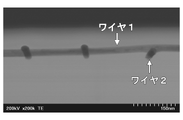
- FIG. 3 is a cross-sectional view of intersections of silver nanowires in the nanostructure network, which constitute the transparent conductive pattern in the transparent conductive film of the present embodiment.
- FIG. 2 is a diagram showing an electron beam diffraction observation field of a nanostructure network that constitutes a transparent conductive pattern in the transparent conductive film of the present embodiment.
- FIG. 4 is a diagram showing electron beam diffraction observation results (diffraction pattern) of silver nanowires away from intersections of silver nanowires in the nanostructure network, which constitute the transparent conductive pattern in the transparent conductive film of the present embodiment.
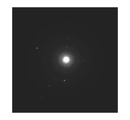
- FIG. 4 is a diagram showing the results of electron beam diffraction observation (diffraction pattern disappearance) in the immediate vicinity of intersections of silver nanowires in the nanostructure network, which constitute the transparent conductive pattern in the transparent conductive film of the present embodiment.
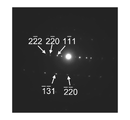
- FIG. 3 is a diagram showing electron beam diffraction observation results (diffraction pattern) of intersections of silver nanowires in a nanostructure network, which constitute a transparent conductive pattern in the transparent conductive film of the present embodiment.
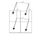
- FIG. 4 is an explanatory diagram of a method for confirming continuity of the laser-processed surface of the transparent conductive film produced in the working example and the comparative processing example.
- FIG. 4 is a judgment image diagram of the transparent conductive films produced in the working example and the comparative working example.
- a transparent conductive film which is a first embodiment of the present invention, comprises a resin film as a base material, and intersections of metal nanowires respectively formed on the first main surface and the second main surface of the base material.
- the light transmittance in the wavelength range of 350 to 700 nm is 80% or more.
- the term “transparent” means that the light transmittance (total light transmittance) in the visible light region (wavelength 400 to 700 nm) is 80% or more.
- the resin film serving as the base material of the transparent conductive film of the present embodiment contains a base resin and an ultraviolet absorber, and has a light transmittance of 10% or less in the wavelength range of 350 to 370 nm in the light transmission spectrum.
- the base resin that is the base material in the light transmission spectrum of a film with the same thickness as the resin film, the light transmission in the ultraviolet light (wavelength 350 to 400 nm) and visible light (wavelength 400 to 700 nm) regions with a wavelength of 350 nm or more.
- a resin with a modulus of 80% or more is used.
- the reason why the resin film has a light transmittance of 10% or less in the wavelength range of 350 to 370 nm will be described later.
- the base resin is not particularly limited as long as it is transparent and non-conductive.
- cycloolefin polymer polycarbonate [PC], polyester (polyethylene terephthalate [PET], polyethylene naphthalate [PEN], etc.), polyolefin (polyethylene [PE], polypropylene [PP], etc.), polyaramide, acrylic resin (polymethyl methacrylate [PMMA], etc.) can be suitably used.
- the resin film containing the base resin may have a single layer or a plurality of layers having functions such as easy adhesion and hard coating within the range that does not impair the optical properties and electrical properties, and may be provided on one side or both sides. good too.
- a cycloolefin polymer is a polymer synthesized using cycloolefins such as norbornene as a monomer, and has an alicyclic structure in its molecular structure.
- Cycloolefin polymers include hydrogenation ring-opening metathesis polymerization type [COP] of norbornene derivatives and addition polymerization type [COC] of ethylene.
- hydrogenation ring-opening metathesis polymerization type [COP] is more preferable from the viewpoint of heat resistance, flex resistance, and the like.
- Hydrogenated ring-opening metathesis polymerization type [COP] includes ZEONEX (registered trademark) and ZEONOR (registered trademark) of Nippon Zeon Co., Ltd. and ARTON (registered trademark) of JSR Corporation.
- the thickness of the resin film is not particularly limited, it is preferably 10 ⁇ m to 200 ⁇ m, more preferably 10 ⁇ m to 100 ⁇ m, still more preferably 10 ⁇ m to 50 ⁇ m.
- the thickness of the resin film is 10 ⁇ m or more, a sufficient effect can be obtained to prevent laser light from penetrating the back surface.
- the thickness of the film is 200 ⁇ m or less, the formability when the film is made into a device and the bending resistance when it is applied to a foldable application are improved.
- UV absorber contained in the resin film.
- benzotriazole-based ultraviolet absorbers triazine-based ultraviolet absorbers, benzophenone-based ultraviolet absorbers, acrylonitrile-based ultraviolet absorbers, salicylic acid-based ultraviolet absorbers, cyanoacrylate-based ultraviolet absorbers, azomethine-based ultraviolet absorbers, indole-based ultraviolet absorbers Absorbents, naphthalimide-based UV absorbers, and phthalocyanine-based UV absorbers can be used.
- benzotriazole-based UV absorbers exhibiting high UV absorbability are preferred.
- Benzotriazole-based UV absorbers contain a benzotriazole structure in the molecule.
- benzotriazole-based UV absorbers include 2,2′-methylenebis[6-(2H-benzotriazol-2-yl-)-4-(1,1,3,3-tetramethylbutyl)phenol], 2-(2H-benzotriazol-2-yl)-p-cresol, and 2-(5-chloro-2H-benzotriazol-2-yl)-6-tert-butyl-4-methylphenol.
- Examples of commercial products of benzotriazole-based ultraviolet absorbers include Adekastab (registered trademark) LA-31, Adekastab LA-32, Adekastab LA-36 (all manufactured by ADEKA Corporation), Tinuvin (registered trademark) 360 (BASF Japan Co., Ltd.).
- the amount of the ultraviolet absorber contained in the resin film is not particularly limited as long as it can suppress the penetration of laser light to the back surface, but it is preferably 0.25% by mass to 10% by mass with respect to the total mass of the resin film, and 0 0.5% to 7.5% by weight is more preferred, and 1% to 5% by weight is even more preferred.
- 0.25% by mass or more is added, the effect of blocking laser light is sufficiently exhibited.
- the amount added is 5% by mass or less, precipitation of the ultraviolet absorber during the production and processing of the resin film can be prevented.
- the transparent conductive film of this embodiment has transparent conductive films (a first transparent conductive film and a second transparent conductive film) on both main surfaces of a resin film that is a substrate.
- Both transparent conductive films contain a nanostructured network with intersections of metal nanowires and a binder resin. Preferably, at least some of the intersections of the metal nanowires are constituted by a fused nanostructure network.
- a dispersion of metal nanowires may be applied onto a substrate and then dried. At least part of the part is fused. It can be confirmed from the analysis of the electron beam diffraction pattern of a transmission electron microscope (TEM) that the intersections of the metal nanowires are fused. Specifically, it can be confirmed by analyzing the electron beam diffraction pattern of the portions where the metal nanowires intersect each other and confirming that the crystal structure has changed (occurrence of recrystallization).
- a known manufacturing method can be used as a method for manufacturing metal nanowires.
- silver nanowires can be synthesized by reducing silver nitrate in the presence of polyvinylpyrrolidone using the Poly-ol method (see Chem. Mater., 2002, 14, 4736).
- Gold nanowires can also be synthesized by reducing chloroauric acid hydrate in the presence of polyvinylpyrrolidone (see J. Am. Chem. Soc., 2007, 129, 1733). Techniques for large-scale synthesis and purification of silver nanowires and gold nanowires are described in detail in WO2008/073143 and WO2008/046058.
- a gold nanotube having a porous structure can be synthesized by reducing a chloroauric acid solution using a silver nanowire as a template.
- the silver nanowires used as the template dissolve into the solution due to the redox reaction with chloroauric acid, resulting in the formation of gold nanotubes having a porous structure (J. Am. Chem. Soc., 2004, 126, 3892- 3901).
- the average diameter of the metal nanowires is preferably 1 to 500 nm, more preferably 5 to 200 nm, even more preferably 5 to 100 nm, and particularly preferably 10 to 50 nm.
- the average length of the long axis of the metal nanowires is preferably 1 to 100 ⁇ m, more preferably 1 to 80 ⁇ m, even more preferably 2 to 70 ⁇ m, and particularly preferably 5 to 50 ⁇ m.
- the metal nanowire preferably has an average diameter thickness and an average major axis length satisfying the above ranges, and an average aspect ratio of more than 5, more preferably 10 or more, and 100 or more. is more preferable, and 200 or more is particularly preferable.
- the aspect ratio is a value obtained by a/b when the average diameter of the metal nanowires is approximated by b and the average length of the long axis by a.
- a and b are measured using a scanning electron microscope (SEM) and an optical microscope.
- b average diameter
- JSM-7000F field emission scanning electron microscope JSM-7000F (manufactured by JEOL Ltd.). determined as the arithmetic mean of the measured values.
- a shape measuring laser microscope VK-X200 manufactured by Keyence Corporation
- VK-X200 manufactured by Keyence Corporation
- Materials for metal nanowires include, for example, at least one selected from the group consisting of gold, silver, platinum, copper, nickel, iron, cobalt, zinc, ruthenium, rhodium, palladium, cadmium, osmium, and iridium, and these metals. A combined alloy and the like are included.
- the binder resin can be applied without limitation as long as it has transparency, but when using metal nanowires using the polyol method, alcohol, water Alternatively, it is preferable to use a binder resin soluble in a mixed solvent of alcohol and water.
- a binder resin soluble in a mixed solvent of alcohol and water examples thereof include hydrophilic cellulosic resins such as poly-N-vinylpyrrolidone, methylcellulose, hydroxyethylcellulose and carboxymethylcellulose, butyral resins, and poly-N-vinylacetamide (PNVA (registered trademark)).
- PNVA poly-N-vinylacetamide
- Poly-N-vinylacetamide is a homopolymer of N-vinylacetamide (NVA).
- N-vinylacetamide copolymer a copolymer containing 70 mol % or more of N-vinylacetamide (NVA) as a monomer unit can also be used.
- NVA N-vinylacetamide
- Monomers that can be copolymerized with NVA include, for example, N-vinylformamide, N-vinylpyrrolidone, acrylic acid, methacrylic acid, sodium acrylate, sodium methacrylate, acrylamide and acrylonitrile.
- the N-vinylacetamide-derived monomer unit is preferably contained in the polymer in an amount of 70 mol% or more, more preferably 80 mol% or more, and more preferably 90 mol% or more. more preferably.
- Such a polymer preferably has a weight average molecular weight of 30,000 to 4,000,000, more preferably 100,000 to 3,000,000, further preferably 300,000 to 1,500,000 in terms of absolute molecular weight.
- the binder resin is water-soluble, the absolute molecular weight is measured by the following method.
- the binder resin is dissolved in the following eluent and left to stand for 20 hours.
- the concentration of the binder resin in this solution is 0.05 mass %.
- GPC Shodex (registered trademark) SYSTEM21 manufactured by Showa Denko K.K.
- the above resins may be used alone or in combination of two or more. When two or more types are combined, simple mixing may be used, or a copolymer may be used.
- the first and second transparent conductive films each contain a nanostructure network having metal nanowire intersections and a binder resin, as described above.
- the first and second transparent conductive films are formed by uniformly dispersing the metal nanowires and applying a metal nanowire ink containing a solvent that dissolves the binder resin to both main surfaces of the resin film by printing or the like, followed by drying and removing the solvent. can be formed by
- the solvent is not particularly limited as long as the metal nanowires are well dispersed and the solvent dissolves the binder resin but does not dissolve the resin film.
- Alcohols are saturated monohydric alcohols (methanol, ethanol, normal propanol and isopropanol) having 1 to 3 carbon atoms represented by C n H 2n+1 OH (n is an integer of 1 to 3) [hereinafter simply “carbon atoms Saturated monohydric alcohol with a number of 1 to 3”. ], and more preferably contains at least 40% by mass of saturated monohydric alcohol having 1 to 3 carbon atoms in all alcohols.
- the use of a saturated monohydric alcohol having 1 to 3 carbon atoms facilitates drying of the solvent, which is advantageous in terms of the process.
- Alcohols other than saturated monohydric alcohols having 1 to 3 carbon atoms can be used in combination as alcohols.
- Alcohols other than saturated monohydric alcohols having 1 to 3 carbon atoms that can be used in combination include, for example, ethylene glycol, propylene glycol, ethylene glycol monomethyl ether, ethylene glycol monoethyl ether, propylene glycol monomethyl ether, and propylene glycol monoethyl ether. mentioned.
- the total alcohol content in the mixed solvent is preferably 5 to 90% by mass. If the alcohol content in the mixed solvent is less than 5% by mass or more than 90% by mass, striped patterns (coating spots) may occur during coating.
- the metal nanowire ink can be produced by stirring and mixing the binder resin, metal nanowires and solvent with a rotation or revolution stirrer or the like.
- the content of the binder resin contained in the metal nanowire ink is preferably in the range of 0.01 to 1.0% by mass.
- the content of metal nanowires contained in the metal nanowire ink is preferably in the range of 0.01 to 1.0% by mass.
- the content of the solvent contained in the metal nanowire ink is preferably in the range of 98.0 to 99.98% by mass.
- Metal nanowire ink can be printed by printing methods such as bar coating, spin coating, spray coating, gravure, and slit coating.
- printing methods such as bar coating, spin coating, spray coating, gravure, and slit coating.
- shape of the printed film or pattern formed by printing it may be the shape of the wiring or electrode pattern formed on the base material, or the film covering the entire surface or a part of the base material ( solid pattern), and the like.
- the formed printed film becomes conductive by drying the solvent.
- the dry thickness of the transparent conductive film is preferably 10 to 300 nm, more preferably 30 to 200 nm, although it varies depending on the diameter of the metal nanowires used, the desired sheet resistance value, and the like.
- the dry thickness of the transparent conductive film is 10 nm or more, the number of intersections of the metal nanowires increases, so good conductivity can be obtained.
- the dry thickness of the transparent conductive film is 300 nm or less, light is easily transmitted and reflection by the metal nanowires is suppressed, so that good optical properties can be obtained. Appropriate light irradiation may be performed on the transparent conductive film as necessary.
- the transparent conductive film of this embodiment has a first protective film on the first transparent conductive film and a second protective film on the second transparent conductive film.
- the protective film that protects the transparent conductive film is a thermosetting film of a curable resin composition.
- the curable resin composition preferably contains (A) a polyurethane containing a carboxy group, (B) an epoxy compound having two or more epoxy groups in the molecule, and (C) a curing accelerator. .
- a curable resin composition is formed on the first and second transparent conductive films by printing, coating, or the like, and cured to form a protective film. Curing of the curable resin composition can be carried out by, for example, heating and drying the thermosetting resin composition to thermally cure it.
- (B) an epoxy compound having two or more epoxy groups in the molecule is simply referred to as "(B) epoxy compound”.
- the polyurethane containing a carboxy group preferably has a weight average molecular weight of 1,000 to 100,000, more preferably 2,000 to 70,000. It is preferably 3,000 to 50,000, and more preferably 3,000 to 50,000.
- the weight-average molecular weight of a polyurethane containing a carboxyl group is a polystyrene-equivalent value measured by GPC.
- the weight average molecular weight of the carboxyl group-containing polyurethane is 100,000 or less, the solubility in a solvent is good, and the viscosity of the polyurethane solution after dissolution does not become too high, resulting in excellent handleability.
- the GPC measurement conditions for polyurethanes containing carboxyl groups are as follows. Apparatus name: HPLC unit HSS-2000 manufactured by JASCO Corporation Column: Shodex column LF-804 Mobile phase: Tetrahydrofuran Flow rate: 1.0 mL/min Detector: RI-2031Plus manufactured by JASCO Corporation Temperature: 40.0°C Sample volume: Sample loop 100 ⁇ l Sample concentration: Prepared to about 0.1% by mass
- the acid value of the carboxy group-containing polyurethane is preferably 10 to 140 mg-KOH/g, more preferably 15 to 130 mg-KOH/g.
- the protective film has good solvent resistance and the resin composition has good curability.
- the solubility of the polyurethane in a solvent is good, and the viscosity of the resin composition can be easily adjusted to a desired viscosity. In addition, problems such as warping of the base film due to excessive hardening of the cured product are less likely to occur.
- Acid value (mg-KOH/g) [B x f x 5.611]/S B: Amount of 0.1N potassium hydroxide-ethanol solution used (ml) f: Factor S of 0.1N potassium hydroxide-ethanol solution: Amount of sample collected (g)
- Polyurethane containing a carboxy group is, more specifically, a polyurethane synthesized using (a1) a polyisocyanate compound, (a2) a polyol compound, and (a3) a dihydroxy compound having a carboxy group as monomers.
- a1 a polyisocyanate compound
- a2) a polyol compound
- a3 a dihydroxy compound having a carboxy group as monomers.
- each of (a1), (a2), and (a3) preferably does not contain a conjugated functional group such as an aromatic compound.
- a conjugated functional group such as an aromatic compound.
- (a1) Polyisocyanate compound As the (a1) polyisocyanate compound, a diisocyanate having two isocyanato groups per molecule is usually used.
- polyisocyanate compounds include aliphatic polyisocyanates and alicyclic polyisocyanates, and these can be used alone or in combination of two or more.
- a small amount of polyisocyanate having 3 or more isocyanato groups can also be used as long as the carboxy group-containing polyurethane does not gel.
- aliphatic polyisocyanates examples include 1,3-trimethylene diisocyanate, 1,4-tetramethylene diisocyanate, 1,6-hexamethylene diisocyanate, 1,9-nonamethylene diisocyanate, 1,10-decamethylene diisocyanate, 2 , 2,4-trimethylhexamethylene diisocyanate, 2,4,4-trimethylhexamethylene diisocyanate, lysine diisocyanate, 2,2′-diethyl ether diisocyanate, dimer acid diisocyanate.
- Alicyclic polyisocyanates include, for example, 1,4-cyclohexanediisocyanate, 1,3-bis(isocyanatomethyl)cyclohexane, 1,4-bis(isocyanatomethyl)cyclohexane, 3-isocyanatomethyl-3,5 ,5-trimethylcyclohexyl isocyanate (IPDI, isophorone diisocyanate), bis-(4-isocyanatocyclohexyl)methane (hydrogenated MDI), hydrogenated (1,3- or 1,4-) xylylene diisocyanate, norbornane diisocyanate. be done.
- IPDI isophorone diisocyanate
- hydrochloride bis-(4-isocyanatocyclohexyl)methane
- hydrogenated 1,3- or 1,4-) xylylene diisocyanate
- norbornane diisocyanate norbornane diisocyanate.
- the content of these is preferably 50 mol% or less, more than It is preferably 30 mol % or less, more preferably 10 mol % or less.
- (a2) Polyol compound (a2) Polyol compound (however, (a2) polyol compound does not include (a3) a dihydroxy compound having a carboxyl group described later) usually has a number average molecular weight of 250 to 50,000. Yes, preferably 400 to 10,000, more preferably 500 to 5,000.
- the number average molecular weight of the polyol compound is a polystyrene-equivalent value measured by GPC under the conditions described above.
- (a2) Polyol compounds include, for example, polycarbonate polyols, polyether polyols, polyester polyols, polylactone polyols, polysilicones with hydroxyl groups on both ends, and C18 (18 carbon atoms) unsaturated fatty acids made from vegetable oils and fats, and It is a polyol compound having 18 to 72 carbon atoms obtained by hydrogenating a polyvalent carboxylic acid derived from the polymer and converting the carboxylic acid into a hydroxyl group.
- the (a2) polyol compound is preferably a polycarbonate polyol from the viewpoint of the balance between water resistance as a protective film, insulation reliability, and adhesion to the substrate.
- a polycarbonate polyol can be obtained by reacting a diol having 3 to 18 carbon atoms as a raw material with a carbonate ester or phosgene, and is represented by the following structural formula (1), for example.
- R 3 is a residue obtained by removing the hydroxyl group from the corresponding diol (HO--R 3 --OH) and is an alkylene group having 3 to 18 carbon atoms, and n 3 is a positive integer, preferably is 2-50.
- the polycarbonate polyol represented by formula (1) is 1,3-propanediol, 1,4-butanediol, 1,5-pentanediol, 1,6-hexanediol, 3-methyl-1 ,5-pentanediol, 1,8-octanediol, 1,3-cyclohexanedimethanol, 1,4-cyclohexanedimethanol, 1,9-nonanediol, 2-methyl-1,8-octanediol, 1,10 -Decamethylene glycol or 1,2-tetradecanediol can be used as a starting material.
- the polycarbonate polyol may be a polycarbonate polyol (copolymerized polycarbonate polyol) having multiple types of alkanediyl groups in its skeleton.
- the use of a copolymerized polycarbonate polyol is often advantageous from the viewpoint of preventing crystallization of (A) polyurethanes containing carboxy groups. Considering solubility in a solvent, it is preferable to use a polycarbonate polyol having a branched skeleton and a hydroxyl group at the end of the branched chain.
- a dihydroxy compound containing a carboxy group (a3)
- the dihydroxy compound containing a carboxy group has two selected from a hydroxy group and a hydroxyalkyl group having 1 or 2 carbon atoms, and has a molecular weight of A carboxylic acid or aminocarboxylic acid having a molecular weight of 200 or less is preferable because the cross-linking point can be controlled.
- Dihydroxy compounds containing a carboxy group include, for example, 2,2-dimethylolpropionic acid, 2,2-dimethylolbutanoic acid, N,N-bishydroxyethylglycine, N,N-bishydroxyethyl Alanine and the like are included, and among these, 2,2-dimethylolpropionic acid and 2,2-dimethylolbutanoic acid are preferred because of their high solubility in solvents.
- the dihydroxy compound containing a carboxy group can be used alone or in combination of two or more.
- (A) Polyurethane containing a carboxyl group can be synthesized only from the above three components ((a1), (a2) and (a3)).
- (a4) a monohydroxy compound and/or (a5) a monoisocyanate compound can also be reacted to synthesize.
- monohydroxy compound and (a5) monoisocyanate compound are preferably compounds containing no aromatic ring or carbon-carbon double bond in the molecule.
- the (A) polyurethane containing a carboxyl group is prepared by using an appropriate organic solvent in the presence or absence of a known urethanization catalyst such as dibutyltin dilaurate, and the above (a1) polyisocyanate compound, ( It can be synthesized by reacting a2) a polyol compound and (a3) a dihydroxy compound having a carboxyl group. (a1) The polyisocyanate compound, (a2) the polyol compound, and (a3) the dihydroxy compound having a carboxyl group are reacted without a catalyst.
- a known urethanization catalyst such as dibutyltin dilaurate
- the organic solvent is not particularly limited as long as it has low reactivity with the isocyanate compound.
- the organic solvent preferably does not contain a basic functional group such as amine and has a boiling point of 50° C. or higher, preferably 80° C. or higher, more preferably 100° C. or higher.
- solvents examples include toluene, xylene, ethylbenzene, nitrobenzene, cyclohexane, isophorone, diethylene glycol dimethyl ether, ethylene glycol diethyl ether, ethylene glycol monomethyl ether acetate, propylene glycol monomethyl ether acetate, Propylene glycol monoethyl ether acetate, dipropylene glycol monomethyl ether acetate, diethylene glycol monoethyl ether acetate, methyl methoxypropionate, ethyl methoxypropionate, methyl ethoxypropionate, ethyl ethoxypropionate, ethyl acetate, acetic acid Mention may be made of n-butyl, isoamyl acetate, ethyl lactate, acetone, methyl ethyl ketone, cyclohexanone, N,N-dimethylformamide,
- the organic solvent is propylene glycol monomethyl ether acetate, propylene glycol mono Ethyl ether acetate, dipropylene glycol monomethyl ether acetate, diethylene glycol monoethyl ether acetate, ⁇ -butyrolactone, or combinations thereof are preferred.
- the order in which the raw materials are added is not particularly limited, but usually (a2) the polyol compound and (a3) the dihydroxy compound having a carboxyl group are first placed in a reaction vessel, dissolved or dispersed in a solvent, and then heated to 20 to 150°C. , more preferably at 60 to 120°C, (a1) the polyisocyanate compound is added dropwise, and then these are reacted at 30 to 160°C, more preferably 50 to 130°C.
- the raw material charging molar ratio is adjusted according to the desired molecular weight and acid value of the polyurethane.
- the molar ratio of (a1) the isocyanato group of the polyisocyanate compound to ((a2) the hydroxyl group of the polyol compound + (a3) the hydroxyl group of the dihydroxy compound having a carboxyl group) is preferably 0.5 to 1.5. :1, more preferably 0.8-1.2:1, more preferably 0.95-1.05:1.
- the molar ratio of (a2) hydroxyl group of the polyol compound to (a3) hydroxyl group of the dihydroxy compound having a carboxyl group is preferably 1:0.1-30, more preferably 1:0.3-10.
- epoxy compounds (B) include bisphenol A type epoxy compounds, hydrogenated bisphenol A type epoxy resins, bisphenol F type epoxy resins, novolak type epoxy resins, phenol novolak type epoxy resins, cresol novolak type epoxy resins, N-glycidyl type epoxy resin, bisphenol A novolac type epoxy resin, chelate type epoxy resin, glyoxal type epoxy resin, amino group-containing epoxy resin, rubber modified epoxy resin, dicyclopentadiene phenolic type epoxy resin, silicone modified epoxy resin, ⁇ Epoxy compounds having two or more epoxy groups in one molecule, such as a caprolactone-modified epoxy resin, an aliphatic epoxy resin containing a glycidyl group, and an alicyclic epoxy resin containing a glycidyl group.
- An epoxy compound having 3 or more epoxy groups in one molecule can be used more preferably.
- examples of such epoxy compounds include EHPE (registered trademark) 3150 (manufactured by Daicel Corporation), jER604 (manufactured by Mitsubishi Chemical Corporation), EPICLON EXA-4700 (manufactured by DIC Corporation), and EPICLON HP-7200 (manufactured by DIC Corporation). company), pentaerythritol tetraglycidyl ether, pentaerythritol triglycidyl ether, and TEPIC-S (manufactured by Nissan Chemical Industries, Ltd.).
- the epoxy compound may have an aromatic ring in the molecule.
- the mass of (B) the epoxy compound is preferably 20% by mass or less with respect to the total mass of (A) the carboxy group-containing polyurethane and (B) the epoxy compound.
- the mixing ratio of (B) the epoxy compound and (A) the carboxy group-containing polyurethane is 0.5 to 1.5 in terms of the equivalent ratio of the carboxy group in the polyurethane to the epoxy group of the (B) epoxy compound. It is preferably from 0.7 to 1.3, even more preferably from 0.9 to 1.1.
- Curing accelerators include, for example, phosphine compounds such as triphenylphosphine and tributylphosphine (manufactured by Hokko Chemical Industry Co., Ltd.), Curesol (registered trademark) (imidazole-based epoxy resin curing agent: Shikoku Kasei Kogyo Co., Ltd.), 2-phenyl-4-methyl-5-hydroxymethylimidazole, U-CAT (registered trademark) SA series (DBU salt: San-Apro Co., Ltd.), Irgacure (registered trademark) 184 .
- phosphine compounds such as triphenylphosphine and tributylphosphine (manufactured by Hokko Chemical Industry Co., Ltd.), Curesol (registered trademark) (imidazole-based epoxy resin curing agent: Shikoku Kasei Kogyo Co., Ltd.), 2-phenyl-4-methyl-5-hydroxymethylimidazole, U-CAT (register
- the amount of the curing accelerator (C) used is too small, the effect of the addition will be lost, and if the amount used is too large, the electrical insulation will decrease. 0.1 to 10% by mass, more preferably 0.5 to 6% by mass, still more preferably 0.5 to 5% by mass, and particularly preferably 0.5 to 3% by mass relative to the total mass of the epoxy compound .
- Curing aids include, for example, polyfunctional thiol compounds and oxetane compounds.
- polyfunctional thiol compounds include pentaerythritol tetrakis(3-mercaptopropionate), tris-[(3-mercaptopropionyloxy)-ethyl]-isocyanurate, trimethylolpropane tris(3-mercaptopropionate).
- Karenz (registered trademark) MT series manufactured by Showa Denko KK
- oxetane compound examples include Aron Oxetane (registered trademark) series (manufactured by Toagosei Co., Ltd.), ETERNACOLL (registered trademark) OXBP and OXMA (manufactured by Ube Industries, Ltd.).
- the amount of the curing aid used is preferably 0.1 to 10 parts by mass, more preferably 0.5 to 6 parts by mass, based on 100 parts by mass of the epoxy compound (B). When added in an amount of 0.1 part by mass or more, the effect of the auxiliary agent is sufficiently exhibited, and when added in an amount of 10 parts by mass or less, curing can be performed at a rate that facilitates handling.
- the curable resin composition preferably contains 95.0% by mass or more and 99.9% by mass or less of the solvent (D), more preferably 96% by mass or more and 99.7% by mass or less. It is more preferable to contain not less than 99.5% by mass and not more than 99.5% by mass.
- the solvent a solvent that does not attack the transparent conductive film or the resin film can be used.
- the solvent used for synthesizing the carboxy group-containing polyurethane can be used as it is, or (A) another solvent is used to adjust the solubility or printability of the carboxy group-containing polyurethane.
- the solvent used for synthesizing (A) the carboxy group-containing polyurethane may be distilled off before and after adding the new solvent to replace the solvent.
- the boiling point of the solvent is preferably 80°C to 300°C, more preferably 80°C to 250°C.
- D If the boiling point of the solvent is 80° C. or higher, it is possible to suppress unevenness caused by excessively quick drying.
- D When the boiling point of the solvent is 300° C. or less, the heat treatment time required for drying and curing can be shortened, and productivity in industrial production can be improved.
- Solvents include propylene glycol monomethyl ether acetate (boiling point 146°C), ⁇ -butyrolactone (boiling point 204°C), diethylene glycol monoethyl ether acetate (boiling point 218°C), tripropylene glycol dimethyl ether (boiling point 243°C), and the like.
- ether solvents such as propylene glycol dimethyl ether (boiling point 97°C) and diethylene glycol dimethyl ether (boiling point 162°C), isopropyl alcohol (boiling point 82°C), t-butyl alcohol (boiling point 82°C), 1 - hexanol (boiling point 157 ° C.), propylene glycol monomethyl ether (boiling point 120 ° C.), diethylene glycol monomethyl ether (boiling point 194 ° C.), diethylene glycol monoethyl ether (boiling point 196 ° C.), diethylene glycol monobutyl ether (boiling point 230 ° C.), triethylene glycol ( (boiling point: 276°C), solvents containing hydroxyl groups such as ethyl lactate (boiling point: 154°C), methyl ethyl ketone (boiling point
- solvents can be used alone or in combination of two or more.
- the solubility of (A) the carboxy group-containing polyurethane, (B) the epoxy compound, etc. should be considered in addition to the solvent used in the synthesis of the (A) carboxy group-containing polyurethane.
- the curable resin composition contains (A) a polyurethane containing a carboxyl group, (B) an epoxy compound, (C) a curing accelerator, and (D) a solvent, and (D) the content of the solvent is 95. 0% by mass or more and 99.9% by mass or less, and stirred so that these components become uniform.
- the solid content concentration in the curable resin composition varies depending on the desired film thickness and printing method, but is preferably 0.1 to 10% by mass, more preferably 0.5% to 5% by mass. preferable.
- the film thickness does not become excessively thick when the curable resin composition is applied on the transparent conductive film, and the electrical connection with the transparent conductive film is maintained.
- the protective film can be provided with weather resistance and light resistance.
- the protective film solid content in the curable resin composition (A) a polyurethane containing a carboxy group, (B) an epoxy compound, and (C) a curing residue in a curing accelerator
- the ratio of the aromatic ring-containing compound defined by the following formula is preferably suppressed to 15% by mass or less.
- (C) curing residue in the curing accelerator used herein means that all or part of the curing accelerator (C) may disappear (decompose, volatilize, etc.) depending on the curing conditions, so it is protected under the curing conditions. It means the (C) curing accelerator remaining in the film.
- (C) curing accelerator remaining in the protective film after curing cannot be accurately quantified, it is calculated based on the charged amount assuming that it does not disappear due to curing conditions, and the ratio of the aromatic ring-containing compound is It is preferable to use (C) the curing accelerator within the range of 15% by mass or less.
- a curable film is formed on a transparent conductive film (also referred to as a “metal nanowire layer”) by a printing method such as a bar coat printing method, a gravure printing method, an inkjet method, or a slit coating method.
- a protective film is formed by applying a resin composition, drying the solvent, and curing the curable resin after removing the solvent.
- the thickness of the protective film obtained after curing is more than 30 nm and 1 ⁇ m or less.
- the thickness of the protective film is preferably more than 50 nm and 500 nm or less, more preferably more than 100 nm and 200 nm or less. If the thickness of the protective film is 1 ⁇ m or less, it becomes easy to conduct with the wiring in the post-process. When the thickness is more than 30 nm, the effect of protecting the metal nanowire layer is sufficiently exhibited.
- a second embodiment of the present invention is a patterned transparent conductive film, comprising a first transparent conductive pattern film on the first main surface of a resin film as a substrate, and a first transparent conductive pattern film on the second main surface. a second transparent conductive pattern film different from the pattern of the transparent conductive pattern film, a first protective film on the first transparent conductive pattern film, and a second protective film on the second transparent conductive pattern film respectively, wherein the first transparent conductive pattern film comprises a first conductive region and a first non-conductive region, and the first conductive region comprises metal nanowires.
- the resin film contains a structural network and a binder resin, the resin film contains a base resin and an ultraviolet absorber, and has a light transmittance of 10% or less in a wavelength region of 350 to 370 nm in the light transmission spectrum, and the base resin, A film having the same thickness as the resin film has a light transmittance of 80% or more in a wavelength region of 350 to 700 nm in a light transmission spectrum.
- the difference from the transparent conductive film of the first embodiment described above is that at least the first transparent conductive film is patterned. That is, the first transparent conductive pattern film is formed on the first main surface of the resin film by patterning the first transparent conductive film.
- the first transparent conductive pattern film consists of a first conductive area and a first non-conductive area. A first conductive region is formed from one or more conductive portions and a first non-conductive region is formed from one or more non-conductive portions.
- the first transparent conductive pattern film is different from the second transparent conductive pattern film formed on the second main surface side.
- “the first transparent conductive pattern film is different from the second transparent conductive pattern film” means that the first conductive region and the first non-conductive region in the first transparent conductive pattern film are different from each other.
- the respective projection positions on the two main surface sides are not the same as the arrangement of the second conductive region and the second non-conductive region of the second transparent conductive pattern film formed on the second main surface side means no.
- the second transparent conductive pattern film consists of only the second conductive area or consists of the second conductive area and the second non-conductive area.
- the second transparent conductive pattern film formed on the second main surface side is a solid transparent conductive film.
- the second transparent conductive pattern film consists of a second conductive region and a second non-conductive region
- the second conductive region is formed from one or more conductive portions and the second non-conductive region.
- a conductive region is formed from one or more non-conductive portions.
- a pulsed The metal forming the nano-structured network with the intersections of the metal nanowires, which constitutes the transparent conductive film, is melted and present in the range that has become non-conductive due to the laser irradiation, thereby exhibiting conductivity. A sufficient network structure cannot be maintained, and the region irradiated with the pulsed laser becomes a non-conductive region.
- the wire-like metal that made up the nanostructured network is broken, and the non-conducting regions now contain fragments of the nanostructured network.
- the fragments include those of various shapes, for example, granular (spherical, elliptical, columnar, etc.) obtained by dividing metal nanowires, and local network structures (including intersections of metal nanowires).
- the non-conductive region as a whole includes those finely divided to the level of non-conductivity (intersections of metal nanowires (cross-shaped fragments), etc.).
- Fragments of the nanostructured network residing within the non-conducting regions can be completely removed, but complete removal increases the contrast between the conducting and non-conducting regions and reduces visibility (bone visible), so it is preferable not to remove it completely. Since the rest of the configuration is the same as that of the transparent conductive film of the first embodiment, description thereof is omitted.
- a third embodiment of the present invention is a method for forming a transparent conductive pattern.
- the resin film contains a base resin and an ultraviolet absorber, has a light transmittance of 10% or less in a wavelength region of 350 to 370 nm in the light transmission spectrum, and the base resin has the same thickness as the resin film.
- the light transmittance in the wavelength range of 350 to 700 nm is 80% or more.
- the transparent conductive film of the first embodiment is obtained by including the transparent conductive film forming step and the protective film forming step, and the patterned film of the second embodiment is obtained by including the pattern forming step.
- a transparent conductive film is obtained.
- the first pattern of the transparent conductive film which is the second embodiment, is formed.
- a second transparent conductive film is formed (transparent conductive film forming step).
- the method of forming the first transparent conductive film and the second transparent conductive film is not particularly limited, but as described above, the dispersion of metal nanowires (metal nanowire ink) may be applied onto the substrate (resin film) and dried. can be formed by From the viewpoint of bending resistance, it is preferable to fuse at least a part of the intersections of the metal nanowires by performing a treatment such as heating or light irradiation during and after drying.
- a dispersion of metal nanowires (metal nanowire ink) a dispersion that does not contain a binder resin is applied on a substrate and dried to form a nanostructure network having intersections of metal nanowires.
- a first transparent conductive film and a second transparent conductive film may be formed by coating the solution on a nanostructure network having intersections of metal nanowires and drying the solution.
- a first protective film is formed on the first transparent conductive film, and a second protective film is formed on the second transparent conductive film (protective film forming step).
- the protective film is formed by printing, coating, or the like the curable resin composition described above on the transparent conductive film, and curing the composition.
- the transparent conductive film has a characteristic absorption peak in the ultraviolet light region in the optical transmission spectrum based on the nanostructured network having the intersections of the metal nanowires that compose it.
- the present inventor found that when a pulsed laser beam having a wavelength in the range of 350 to 370 nm and a pulse width shorter than 1 nanosecond is applied to the first transparent conductive film from the side of the first protective film, the second transparent conductive film It has been found that the conductive film is not etched and only the first transparent conductive film can be selectively etched.
- Pulse widths longer than 1 nanosecond will cause extra thermal damage to the surroundings. Since the nanostructure network having the intersections of metal nanowires has an absorption peak in the ultraviolet region in the light transmission spectrum, it can be etched with a pulsed laser beam in the above wavelength range close to the absorption peak maximum wavelength. .
- the method for forming a transparent conductive pattern according to the third embodiment of the present invention is applied to the transparent conductive film according to the first embodiment of the present invention. That is, by using a resin film having a low light transmittance in the above wavelength range as a base material, it is possible to suppress the arrival of laser light to the second transparent conductive film, and the first transparent conductive film It is considered that only the etching process became possible.
- the second transparent conductive film is different from the first transparent conductive pattern film consisting of the first conductive region and the first non-conductive region formed in the first transparent conductive film with respect to the second transparent conductive film.
- a second transparent conductive pattern film can be formed comprising conductive areas and second non-conductive areas.
- the first transparent conductive pattern film is different from the second transparent conductive pattern film
- the second transparent conductive pattern film can be left as a solid transparent conductive film without etching, that is, without forming the second non-conductive region.
- the pulse width of the pulsed laser is preferably less than 0.1 (100 picoseconds) nanoseconds, more preferably less than 0.01 nanoseconds (10 picoseconds), 0.001 nanoseconds (1 picosecond) ), i.e. femtosecond pulsed lasers are more preferably used.
- the metal nanowires constituting the transparent conductive film that existed in the range that was irradiated with the pulse laser and became the non-conductive region.
- the metal forming the nanostructured network with intersections melts and cannot maintain a sufficient network structure to develop electrical conductivity.
- the wire-like metal that made up the nanostructured network is broken and the non-conductive regions now contain fragments of the nanostructured network.
- the fragments include those of various shapes, for example, nanowires cut into granules (spherical, elliptical, columnar, etc.), and local network structures (including intersections of metal nanowires).
- the remaining non-conductive regions as a whole include those that are finely divided to the level of non-conductivity (intersections of metal nanowires (cross-shaped fragments), etc.). Fragments of the nanostructure network generated in the non-conductive regions due to the etching process can be completely removed, but complete removal increases the contrast between the conductive and non-conductive regions, resulting in poor visibility. It is preferable not to remove it completely because it will decrease (bone will be more visible).
- 100 g of silver nanowire ink was prepared by stirring in an air atmosphere (rotational speed: 100 rpm).
- the concentration of silver nanowires contained in the obtained silver nanowire ink was measured with a Varian AA280Z Zeeman atomic absorption spectrophotometer.
- A4 size corona discharge surface treatment device Wedge Co., Ltd.
- A4SW-FLNW type is used
- A4 size cycloolefin polymer (COP) film G+13 also known as ZF12-013, Nippon Zeon Co., Ltd., thickness 13 ⁇ m
- Both main surfaces were subjected to corona discharge treatment (conveyance speed: 3 m/min, number of treatments: 2 times, output: 0.3 kW).
- a COP film subjected to corona discharge treatment Using a COP film subjected to corona discharge treatment, a TQC automatic film applicator standard (manufactured by Kotec Co., Ltd.), and a wireless bar coater OSP-CN-22L (manufactured by Kotec Co., Ltd.), the wet film thickness was adjusted to 22 ⁇ m.
- a silver nanowire ink was applied to the entire first main surface of the COP film (coating speed: 500 mm/sec). After that, it was dried with hot air at 80° C. for 3 minutes in a thermostat HISPEC HS350 (manufactured by Kusumoto Kasei Co., Ltd.) in an air atmosphere to form a first transparent conductive film (silver nanowire layer).
- the COP film G+13 (also known as ZF12-013, manufactured by Nippon Zeon Co., Ltd., thickness 13 ⁇ m) used as the base material is a resin film containing an ultraviolet absorber. It was confirmed by the following analysis that the film contained 4.9% by mass of the benzotriazole-based ultraviolet absorber with respect to the total mass of the film.
- the light transmission spectrum thereof is shown in FIG. 1 together with the light transmission spectrum of a COP film ZF14-013 (manufactured by Nippon Zeon Co., Ltd., thickness 13 ⁇ m) containing no ultraviolet absorber.
- Quantification of the ultraviolet absorber contained in G+13 was performed by the following method. First, G + 13 was immersed in THF (tetrahydrofuran, manufactured by Fujifilm Wako Pure Chemical Industries, Ltd. (for high-performance liquid chromatography)), and the supernatant was analyzed by LC-MS (ionization method, LC: Ultimate 3000 (manufactured by Dionex), MS: OrbitrapElite ( The chemical structure of the UV absorber was determined by analysis with Therm Fisher Sientifc). Subsequently, the content was quantified using 1 H-NMR (AvIII400 manufactured by Bruker). G+13 was dissolved in cyclohexane (manufactured by Junsei Chemical Co., Ltd.
- HMTCS Hexamethylcyclotrisiloxane
- acetone-d6 deuteration rate 99.9%, for NMR, manufactured by Kanto Chemical Co., Ltd.
- the light transmission spectrum of the resin film was measured by the following method. G+13 and ZF14-013 (denoted as ZF14) were each cut into 3 cm ⁇ 3 cm to prepare test pieces. The transmission spectrum was measured in the wavelength range from 200 nm to 1100 nm using the test piece and an ultraviolet-visible spectrophotometer UV-2400PC (manufactured by Shimadzu Corporation). Table 1 shows the transmittance of the resin film obtained by measurement at 350 nm to 370 nm.
- ⁇ Film thickness measurement> The film thicknesses of the transparent conductive films (silver nanowire layers) formed on both main surfaces were measured using a film thickness measurement system F20-UV (manufactured by Filmetrics Co., Ltd.) based on light interferometry. The average value obtained by measuring three points at different measurement points was used as the film thickness. The spectrum from 450 nm to 800 nm was used for analysis. According to this measurement system, the film thickness (Tc) of the transparent conductive film (silver nanowire layer) formed on the transparent substrate can be directly measured. Table 1 shows the measurement results.
- the temperature of the reaction solution is lowered to 70° C., and the (a1) polyisocyanate compound Desmodur (registered trademark)-W (bis-(4-isocyanatocyclohexyl)methane) manufactured by Sumika Covestro Urethane Co., Ltd. is added by a dropping funnel. ) 59.69 g was added dropwise over 30 minutes. After completion of the dropwise addition, the temperature was raised to 120°C and the reaction was carried out at 120°C for 6 hours. After confirming by IR that the isocyanate had almost disappeared, 0.5 g of isobutanol was added and the reaction was further carried out at 120°C for 6 hours. gone.
- the weight average molecular weight of the obtained carboxy group-containing polyurethane (A) determined by GPC was 32,300, and the acid value of the carboxy group-containing polyurethane (A) was 35.8 mgKOH/g.
- ⁇ Formation of protective film (overcoat layer)> A silver nanowire layer (first transparent conductive film), using a TQC automatic film applicator standard (manufactured by Kotec Co., Ltd.) and a wireless bar coater OSP-CN-05M (manufactured by Kotec Co., Ltd.), the curable resin composition 1 so that the wet film thickness is 5 ⁇ m. was applied to the entire surface (coating speed: 333 mm/sec). After that, hot air drying (thermal curing) was performed in an air atmosphere at 80° C. for 1 minute in a thermostat HISPEC HS350 (manufactured by Kusumoto Kasei Co., Ltd.) to form a first protective film.
- TQC automatic film applicator standard manufactured by Kotec Co., Ltd.
- OSP-CN-05M manufactured by Kotec Co., Ltd.
- a second transparent conductive film (silver nanowire layer) and a second protective film are sequentially formed on the second main surface of the COP film in the same manner as above, A transparent conductive film having conductive layers on both sides was produced.
- a carbon protective layer was additionally formed for 10 seconds using the above-mentioned carbon vapor deposition apparatus again to form a carbon layer with a total thickness of about 80 nm in a state in which markings could be discerned. This protected the AgNWs from damage due to FIB processing, and made the top protective film not interfere with the nanowires when observed with a TEM.
- tungsten deposition was performed using the FIB processing apparatus for 10 minutes to form a tungsten protective layer of 12 ⁇ m in the longitudinal direction of the AgNW, 2 ⁇ m in the orthogonal direction, and 1 ⁇ m in thickness.
- the area around the tungsten protective film was excavated to a depth of about 15 ⁇ m with an FIB, and the layer below the tungsten protective film containing the AgNW intersections was cut out and fixed to a copper mesh.
- the thinned sample was observed using a transmission electron microscope (TEM) HF-2200 (acceleration voltage 200 kV) manufactured by Hitachi High-Tech Co., Ltd. As a result, it was found that one AgNW was stored in the sample in the horizontal direction, and many intersections with AgNWs extending from the depth toward the front were obtained. At the intersection, the boundary between the AgNW (wire 1) in the left-right direction and the AgNW (wire 2) in the frontward direction from the depth became ambiguous, suggesting fusion (FIG. 2).
- TEM transmission electron microscope
- Comparative coating example 1 The same as Example Coating Example 1 except that a cycloolefin polymer (COP) film ZF14-013 (manufactured by Nippon Zeon Co., Ltd., thickness 13 ⁇ m) that does not contain an ultraviolet absorber was used as a base material for producing a transparent conductive film. was carried out on Strictly speaking, ZF14-013 is estimated to have a different composition from the base resin ZF12 of the COP film G+13 used as the substrate in Practical Coating Example 1, but both ZF14 and ZF12 are COP films manufactured by Zeon Corporation.
- COP cycloolefin polymer
- G+13, and ZF14 are isotropic COP films, so the optical properties ([total] light transmittance) at the same thickness of the isotropic film of the base resin ZF12 of G+13 and ZF14 are approximately the same ( ZF14 can be regarded as equivalent to the base resin ZF12 of G+13).
- ⁇ Sheet resistance measurement of silver nanowire layer> A 3 cm ⁇ 3 cm test piece was cut from a transparent conductive film (silver nanowire film) in which a silver nanowire layer and a protective film were sequentially formed on both sides of a resin film, and a resistivity meter Loresta GP (Mitsubishi Chemical Corporation) based on the four-terminal method was used. Analyticc) was used to measure the sheet resistance of each silver nanowire layer. ESP mode was used as the measurement mode and terminals used.
- the transmittance of the transparent conductive film (silver nanowire film) in the wavelength region of 350 to 370 nm (ultraviolet light region) was measured in the same manner as the method for measuring the light transmission spectrum of the resin film described above.
- Table 1 shows the measurement results.
- the transmittance in the wavelength range of 400 to 700 nm (visible light range) is low. Since the transmittance (total light transmittance) in the light region) is sufficiently high, it can be used as a transparent conductive film without any problem.
- the film thickness of the protective film was measured using a film thickness measurement system F20-UV (manufactured by Filmetrics Co., Ltd.) based on the optical interferometry, as in the film thickness of the silver nanowire layer described above. The average value obtained by measuring three points at different measurement points was used as the film thickness. The spectrum from 450 nm to 800 nm was used for analysis. According to this measurement system, the total film thickness (Tc+Tp) of the film thickness (Tc) of the silver nanowire layer formed on the transparent substrate and the film thickness (Tp) of the protective film formed thereon can be directly measured. Therefore, the film thickness (Tp) of the protective film is obtained by subtracting the previously measured film thickness (Tc) of the silver nanowire layer from this measured value. Table 1 shows the measurement results.
- solid lines representing the lattice represent etching lines formed by patterning, and arrows represent the needles.
- ⁇ , ⁇ , ⁇ , and ⁇ are separated by the etching lines by applying the tips of two arrows (needles) connected by corresponding dashed lines to the inside (non-etched region) of the lattice. This indicates that the resistance value between the two regions is measured.
- FIG. 8 shows the judgment image of ⁇ and ⁇ in the comprehensive evaluation.
- FIG. 8 shows the case where the etching process is performed by irradiating the pulse laser from the processed surface side and the pulse laser is not irradiated from the back surface side.
- the case where the pulse laser did not penetrate to the back side and the "conduction" was maintained on the back side is indicated by ⁇ , and the case where the pulse laser penetrated to the back side and the "conduction” was not maintained on the back side.
- the laser used for etching was a picosecond pulse laser (pulse width 15 ps (15 ⁇ 10 -3 ns), frequency: 500 kHz, processing speed 4000 mm / s, output 0.1 W). Measured and evaluated.
- Comparative processing example 1 Measurement and evaluation were carried out in the same manner as in Working Example 1, except that the film of Comparative Coating Example 1 was used as the transparent conductive film used for etching.
- Comparative processing example 2 Measurement and evaluation were carried out in the same manner as in Working Example 1, except that the laser used for etching was a nanosecond pulse laser (pulse width: 180 ns, frequency: 90 kHz, processing speed: 500 mm/s, output: 0.2 W). Model 5330 manufactured by ESI was used as a processing apparatus.
Landscapes
- Engineering & Computer Science (AREA)
- Chemical & Material Sciences (AREA)
- Organic Chemistry (AREA)
- Theoretical Computer Science (AREA)
- General Engineering & Computer Science (AREA)
- Physics & Mathematics (AREA)
- Materials Engineering (AREA)
- Manufacturing & Machinery (AREA)
- Life Sciences & Earth Sciences (AREA)
- Wood Science & Technology (AREA)
- Health & Medical Sciences (AREA)
- Chemical Kinetics & Catalysis (AREA)
- Medicinal Chemistry (AREA)
- Polymers & Plastics (AREA)
- General Physics & Mathematics (AREA)
- Human Computer Interaction (AREA)
- Spectroscopy & Molecular Physics (AREA)
- Dispersion Chemistry (AREA)
- Inorganic Chemistry (AREA)
- Non-Insulated Conductors (AREA)
- Laminated Bodies (AREA)
Abstract
Description
なお、本明細書において「透明」とは、可視光(波長400~700nm)領域での光線透過率(全光線透過率)が80%以上であることをいう。
本実施形態の透明導電フィルムの基材となる樹脂フィルムは、ベース樹脂と紫外線吸収剤とを含み、光透過スペクトルにおいて、波長350~370nmの領域における光線透過率が10%以下である。母材となるベース樹脂としては、上記樹脂フィルムと同じ厚さのフィルムの光透過スペクトルにおいて、波長350nm以上の紫外光(波長350~400nm)、可視光(波長400~700nm)領域での光線透過率が80%以上である樹脂を用いる。母材であるベース樹脂に紫外線吸収剤を含有させた樹脂フィルムは、可視光(波長400~700nm)領域での光線透過率を低下させることなく、波長350~370nmの領域における光線透過率を低下させることができる。樹脂フィルムの波長350~370nmの領域における光線透過率を10%以下とする理由については、後述する。
樹脂フィルムに含有される紫外線吸収剤には特に制限はない。、例えば、ベンゾトリアゾール系紫外線吸収剤、トリアジン系紫外線吸収剤、ベンゾフェノン系紫外線吸収剤、アクリロニトリル系紫外線吸収剤、サリチル酸系紫外線吸収剤、シアノアクリレート系紫外線吸収剤、アゾメチン系紫外線吸収剤、インドール系紫外線吸収剤、ナフタルイミド系紫外線吸収剤、フタロシアニン系紫外線吸収剤が挙げられる。中でも、高い紫外線吸収能を示すベンゾトリアゾール系紫外線吸収剤が好ましい。
本実施形態の透明導電フィルムは、基材である樹脂フィルムの両主面上にそれぞれ透明導電膜(第一の透明導電膜及び第二の透明導電膜)を有する。
下記溶離液にバインダー樹脂を溶解させ、20時間静置する。この溶液におけるバインダー樹脂の濃度は0.05質量%である。
GPC:昭和電工株式会社製Shodex(登録商標)SYSTEM21
カラム:東ソー株式会社製TSKgel(登録商標)G6000PW
カラム温度:40℃
溶離液:0.1mol/L NaH2PO4水溶液+0.1mol/L Na2HPO4水溶液
流速:0.64mL/min
試料注入量:100μL
MALS検出器:ワイアットテクノロジーコーポレーション、DAWN(登録商標) DSP
レーザー波長:633nm
多角度フィット法:Berry法
本実施形態の透明導電フィルムは、第一の透明導電膜上に第一の保護膜、第二の透明導電膜上に第二の保護膜、をそれぞれ有する。
(A)カルボキシ基を含有するポリウレタンは、その重量平均分子量が1,000~100,000であることが好ましく、2,000~70,000であることがより好ましく、3,000~50,000であるとさらに好ましい。本明細書において、カルボキシ基を含有するポリウレタンの重量平均分子量は、GPCで測定したポリスチレン換算の値である。カルボキシ基を含有するポリウレタンの重量平均分子量が1,000以上であると、印刷後の塗膜の伸度、可撓性、並びに強度が十分発揮される。カルボキシ基を含有するポリウレタンの重量平均分子量が100,000以下であると、溶媒への溶解性が良好で、かつ、溶解後のポリウレタン溶液の粘度も高くなりすぎず、ハンドリング性に優れる。
装置名:日本分光株式会社製HPLCユニット HSS-2000
カラム:ShodexカラムLF-804
移動相:テトラヒドロフラン
流速 :1.0mL/min
検出器:日本分光株式会社製 RI-2031Plus
温度 :40.0℃
試料量:サンプルル-プ 100μリットル
試料濃度:約0.1質量%に調製
100ml三角フラスコに試料約0.2gを精密天秤にて精秤し、これにエタノール/トルエン=1/2(質量比)の混合溶媒10mlを加えて溶解する。さらに、この容器に指示薬としてフェノールフタレインエタノール溶液を1~3滴添加し、試料が均一になるまで十分に攪拌する。これを、0.1N水酸化カリウム-エタノール溶液で滴定し、指示薬の微紅色が30秒間続いたときを、中和の終点とする。下記の計算式を用いて得た値を、カルボキシ基を含有するポリウレタンの酸価とする。
酸価(mg-KOH/g)=〔B×f×5.611〕/S
B:0.1N水酸化カリウム-エタノール溶液の使用量(ml)
f:0.1N水酸化カリウム-エタノール溶液のファクター
S:試料の採取量(g)
(a1)ポリイソシアネート化合物としては、通常、1分子当たりのイソシアナト基が2個であるジイソシアネートが用いられる。ポリイソシアネート化合物としては、例えば、脂肪族ポリイソシアネート、脂環式ポリイソシアネートが挙げられ、これらを単独で又は2種以上を組み合わせて用いることができる。カルボキシ基を含有するポリウレタンがゲル化をしない範囲で、イソシアナト基を3個以上有するポリイソシアネートも少量使用することができる。
(a2)ポリオール化合物(ただし、(a2)ポリオール化合物には、後述する(a3)カルボキシ基を有するジヒドロキシ化合物は含まれない。)の数平均分子量は通常250~50,000であり、好ましくは400~10,000、より好ましくは500~5,000である。ポリオール化合物の数平均の分子量は前述した条件でGPCにより測定したポリスチレン換算の値である。
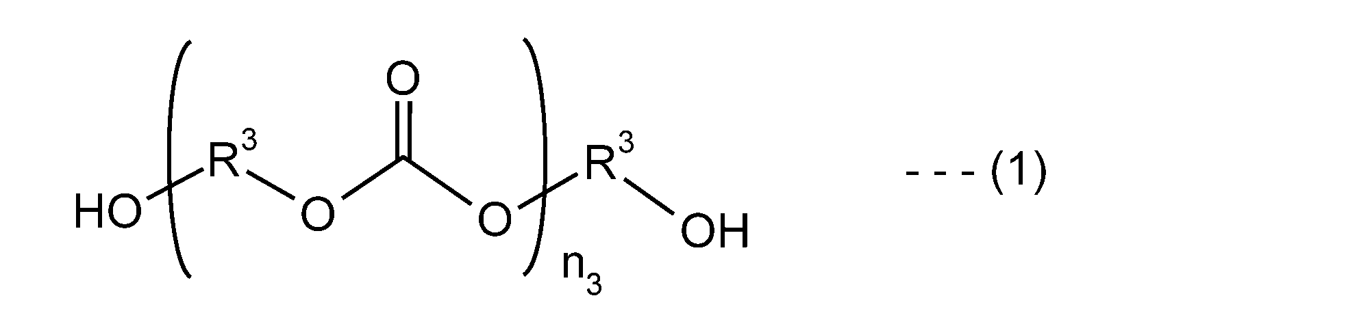
(a3)カルボキシ基を含有するジヒドロキシ化合物としては、ヒドロキシ基、炭素原子数が1又は2のヒドロキシアルキル基から選択されるいずれかを2つ有する、分子量が200以下のカルボン酸又はアミノカルボン酸であることが架橋点を制御できる点で好ましい。(a3)カルボキシ基を含有するジヒドロキシ化合物としては、例えば、2,2-ジメチロ-ルプロピオン酸、2,2-ジメチロ-ルブタン酸、N,N-ビスヒドロキシエチルグリシン、N,N-ビスヒドロキシエチルアラニン等が挙げられ、これらの中でも、溶媒への溶性が高いことから、2,2-ジメチロ-ルプロピオン酸及び2,2-ジメチロ-ルブタン酸が好ましい。(a3)カルボキシ基を含有するジヒドロキシ化合物は、単独で又は2種以上を組み合わせて用いることができる。
(B)エポキシ化合物としては、ビスフェノールA型エポキシ化合物、水添ビスフェノールA型エポキシ樹脂、ビスフェノールF型エポキシ樹脂、ノボラック型エポキシ樹脂、フェノールノボラック型エポキシ樹脂、クレゾールノボラック型エポキシ樹脂、N-グリシジル型エポキシ樹脂、ビスフェノールAのノボラック型エポキシ樹脂、キレート型エポキシ樹脂、グリオキザール型エポキシ樹脂、アミノ基含有エポキシ樹脂、ゴム変性エポキシ樹脂、ジシクロペンタジエンフェノリック型エポキシ樹脂、シリコーン変性エポキシ樹脂、ε-カプロラクトン変性エポキシ樹脂、グリシジル基を含有した脂肪族型エポキシ樹脂、グリシジル基を含有した脂環式エポキシ樹脂などの一分子中に2個以上のエポキシ基を有するエポキシ化合物を挙げることができる。
(C)硬化促進剤としては、例えば、トリフェニルホスフィン、トリブチルホスフィンなどのホスフィン系化合物(北興化学工業株式会社製)、キュアゾール(登録商標)(イミダゾール系エポキシ樹脂硬化剤:四国化成工業株式会社製)、2-フェニル-4-メチル-5-ヒドロキシメチルイミダゾール、U-CAT(登録商標)SAシリーズ(DBU塩:サンアプロ株式会社製)、Irgacure(登録商標)184が挙げられる。(C)硬化促進剤の使用量は、使用量があまりに少ないと添加した効果が無く、使用量が多すぎると電気絶縁性が低下するので、(A)カルボキシ基を含有するポリウレタンと(B)エポキシ化合物の合計質量に対して0.1~10質量%、より好ましくは0.5~6質量%、さらに好ましくは0.5~5質量%、特に好ましくは0.5~3質量%である。
硬化性樹脂組成物には(D)溶媒を95.0質量%以上99.9質量%以下含むことが好ましく、96質量%以上99.7質量%以下含むことがより好ましく、97質量%以上99.5質量%以下含むことがさらに好ましい。(D)溶媒としては、透明導電膜や樹脂フィルムを侵さないものを使用することができる。(A)カルボキシ基を含有するポリウレタンの合成に用いた溶媒をそのまま使用することもできるし、(A)カルボキシ基を含有するポリポリウレタンの溶解性又は印刷性を調整するために他の溶媒を用いることもできる。他の溶媒を用いる場合には、新たな溶媒を添加する前後に(A)カルボキシ基を含有するポリウレタンの合成に用いた溶媒を留去し、溶媒を置換してもよい。操作の煩雑性やエネルギーコストを考えると、(A)カルボキシ基を含有するポリウレタンの合成に用いた溶媒の少なくとも一部をそのまま用いることが好ましい。保護膜用樹脂組成物の安定性を考慮すると、溶媒の沸点は、80℃から300℃であることが好ましく、80℃から250℃であることがより好ましい。(D)溶媒の沸点が80℃以上であると、速乾過ぎることにより生じるムラを抑制することができる。(D)溶媒の沸点が300℃以下であると、乾燥・硬化に要する加熱処理時間を短くすることができ、工業生産時の生産性を向上させることができる。
芳香環含有化合物の割合=[(芳香環含有化合物使用量)/(保護膜の質量((A)カルボキシ基を含有するポリウレタン質量+(B)エポキシ化合物質量+(C)硬化促進剤における硬化残基質量)]×100(%)
<透明導電フィルムの作製>
<銀ナノワイヤ合成>
200mLガラス容器にプロピレングリコール100g(富士フイルム和光純薬株式会社製)を秤量し、金属塩として硝酸銀2.3g(13mmol)(東洋化学工業株式会社製)を加えて室温で2時間撹拌することで硝酸銀溶液(第二溶液)を調製した。
得られた銀ナノワイヤ粗分散液を水2000mlに分散させ、卓上小型試験機(日本ガイシ株式会社製、セラミック膜フィルター セフィルト使用、膜面積0.24m2、孔径2.0μm、寸法Φ30mm×250mm、ろ過差圧0.01MPa)に流し入れ、循環流速12L/min、分散液温度25℃にてクロスフロー濾過を実施し不純物を除去し、銀ナノワイヤ(平均直径:26nm、平均長さ:20μm)を得た。クロスフローろ過しながらエタノール置換を行い、最終的に水/エタノール混合溶媒の分散液(銀ナノワイヤ濃度3質量%、水/エタノール=41/56[質量比])を得た。得られた銀ナノワイヤの平均径の算出には、電界放出形走査電子顕微鏡JSM-7000F(日本電子株式会社製)を用い、任意に選択した100本の銀ナノワイヤ寸法(径)を測定し、その算術平均値を求めた。また、得られた銀ナノワイヤの平均長さの算出には、形状測定レーザマイクロスコープVK-X200(キーエンス株式会社製)を用い、任意に選択した100本の銀ナノワイヤ寸法(長さ)を測定し、その算術平均値を求めた。
上記ポリオール法で合成した銀ナノワイヤの水/エタノール混合溶媒の分散液5g(銀ナノワイヤ濃度3質量%、水/エタノール=41/56[質量比])、水6.4g、メタノール20g(富士フイルム和光純薬株式会社製)、エタノール39g(富士フイルム和光純薬株式会社製)、プロピレングリコールモノメチルエーテル(PGME、富士フイルム和光純薬株式会社製)25g、プロピレングリコール3g(PG、旭硝子株式会社製)、PNVA(登録商標)水溶液(昭和電工株式会社製、固形分濃度10質量%、重量平均分子量90万)1.8gを混合し、ミックスローターVMR-5R(アズワン株式会社製)で1時間、室温、大気雰囲気下で撹拌(回転速度100rpm)して銀ナノワイヤインク100gを作製した。最終的な混合比[質量比]は、銀ナノワイヤ/PNVA/水/メタノール/エタノール/PGME/PG=0.15/0.18/10/20/42/25/3であった。
A4size用コロナ放電表面処理装置(ウェッジ株式会社製)A4SW-FLNW型を用い、基材として用いるA4サイズのシクロオレフィンポリマー(COP)フィルムG+13(別名ZF12-013、日本ゼオン株式会社製、厚み13μm)の両方の主面にコロナ放電処理(搬送速度:3m/min、処理回数:2回、出力:0.3kW)を施した。コロナ放電処理を施したCOPフィルムと、TQC自動フィルムアプリケータースタンダード(コーテック株式会社製)と、ワイヤレスバーコータOSP-CN-22L(コーテック株式会社製)とを用い、ウェット膜厚が22μmとなるように銀ナノワイヤインクをCOPフィルムの第一の主面全面に塗布した(塗工速度500mm/sec)。その後、恒温器HISPEC HS350(楠本化成株式会社製)で80℃、3分間、大気雰囲気下で熱風乾燥し、第一の透明導電膜(銀ナノワイヤ層)を形成した。
両方の主面に形成された透明導電膜(銀ナノワイヤ層)の膜厚は光干渉法に基づく膜厚測定システムF20-UV(フィルメトリクス株式会社製)を用いて測定した。測定箇所を変え、3点測定した平均値を膜厚として用いた。解析には450nmから800nmのスペクトルを用いた。この測定システムによると、透明基材上に形成された透明導電膜(銀ナノワイヤ層)の膜厚(Tc)が直接測定できる。測定結果を表1に示す。
(A)カルボキシ基を含有するポリウレタンの合成例
攪拌装置、温度計、コンデンサーを備えた2L三口フラスコに、(a2)ポリオール化合物としてC-1015N(株式会社クラレ製、ポリカーボネートジオール、原料ジオールモル比:1,9-ノナンジオール:2-メチル-1,8-オクタンジオール=15:85、分子量964)42.32g、(a3)カルボキシ基を含有するジヒドロキシ化合物として2,2-ジメチロールブタン酸(日本化成株式会社製)27.32g、及び溶媒としてジエチレングリコールモノエチルエーテルアセテート(株式会社ダイセル製)158gを仕込み、90℃で上記2,2-ジメチロールブタン酸を溶解させた。
基材である樹脂フィルム(COPフィルムG+13(別名ZF12-013、日本ゼオン株式会社製、厚み13μm))の一方の(第一の)主面上に形成された銀ナノワイヤ層(第一の透明導電膜)の上に、TQC自動フィルムアプリケータースタンダード(コーテック株式会社製)とワイヤレスバーコータOSP-CN-05M(コーテック株式会社製)を用い、ウェット膜厚が5μmになるように硬化性樹脂組成物1を全面に塗布した(塗工速度333mm/sec)。その後、恒温器HISPEC HS350(楠本化成株式会社製)で80℃、1分間、大気雰囲気下で熱風乾燥(熱硬化)し、第一の保護膜を形成した。
金属ナノワイヤ(銀ナノワイヤ)交差部の融着の状態を確認するため、保護膜を形成する前、即ち、銀ナノワイヤ(AgNW)層が塗工されたCOPフィルムに対し、真空デバイス製真空蒸着装置VE-2030を用いて電流値50Aでカーボン棒を用いた蒸着を5秒間行い、ナノワイヤ直上にカーボン保護層を製膜した。次にFIB(収束イオンビーム)加工装置FB-2100(加速電圧40kV)を用いてAgNWとAgNWが90°に近い角度で交差している交点を確認し、交点を含むAgNWの延長線上に線状のマーキングを施しAgNWの目印とした。
透明導電フィルムの作製に、基材として紫外線吸収剤を含まないシクロオレフィンポリマー(COP)フィルムZF14-013(日本ゼオン株式会社製、厚み13μm)を用いたこと以外は、実施塗工例1と同様に実施した。ZF14-013は実施塗工例1で基材として用いたCOPフィルムG+13のベース樹脂ZF12とは厳密には組成が異なると推定されるが、ZF14、ZF12とも日本ゼオン株式会社製のCOPフィルムであり、G+13、ZF14とも等方性のCOPフィルムであることから、G+13のベース樹脂ZF12の等方性フィルムとZF14との同一厚みでの光学特性([全]光線透過率)は略同等である(ZF14をG+13のベース樹脂ZF12と同等とみなせる)と判断している。
樹脂フィルムの両面にそれぞれ銀ナノワイヤ層、保護膜が順次形成された透明導電フィルム(銀ナノワイヤフィルム)から3cm×3cmの試験片を切り出し、4端子法に基づく抵抗率計ロレスタGP(株式会社三菱化学アナリテック製)で銀ナノワイヤ層のシート抵抗をそれぞれ測定した。測定モード及び使用端子はESPモードを用いた。
樹脂フィルムの両面にそれぞれ銀ナノワイヤ層、保護膜が順次形成された透明導電フィルム(銀ナノワイヤフィルム)の3cm×3cmの試験片を用い、ヘーズメーターCOH7700(日本電色工業株式会社製)で測定した。波長400~700nmの透過率(全光線透過率)はJIS K 7361-1に基づき、ヘーズはJIS K 7136に基づいて測定した。同様に樹脂フィルム単独での波長400~700nmの透過率(全光線透過率)も測定した。また、透明導電フィルム(銀ナノワイヤフィルム)の波長350~370nmの領域(紫外光領域)の透過率を前述の樹脂フィルムの光透過スペクトルの測定方法同様に測定した。測定結果を表1に示す。表1に示される測定値から明らかな通り、実施塗工例1は、用いた樹脂フィルムの波長350~370nmの領域(紫外光領域)の透過率は低いものの、波長400~700nmの領域(可視光領域)の透過率(全光線透過率)が十分に高いため、透明導電フィルムとして問題なく使用可能である。
保護膜の膜厚は、前述の銀ナノワイヤ層の膜厚同様光干渉法に基づく膜厚測定システムF20-UV(フィルメトリクス株式会社製)を用いて測定した。測定箇所を変え、3点測定した平均値を膜厚として用いた。解析には450nmから800nmのスペクトルを用いた。この測定システムによると、透明基材上に形成された銀ナノワイヤ層の膜厚(Tc)とその上に形成された保護膜の膜厚(Tp)との総膜厚(Tc+Tp)が直接測定できるので、この測定値から先に測定した銀ナノワイヤ層の膜厚(Tc)を差し引くことにより保護膜の膜厚(Tp)が得られる。測定結果を表1に示す。
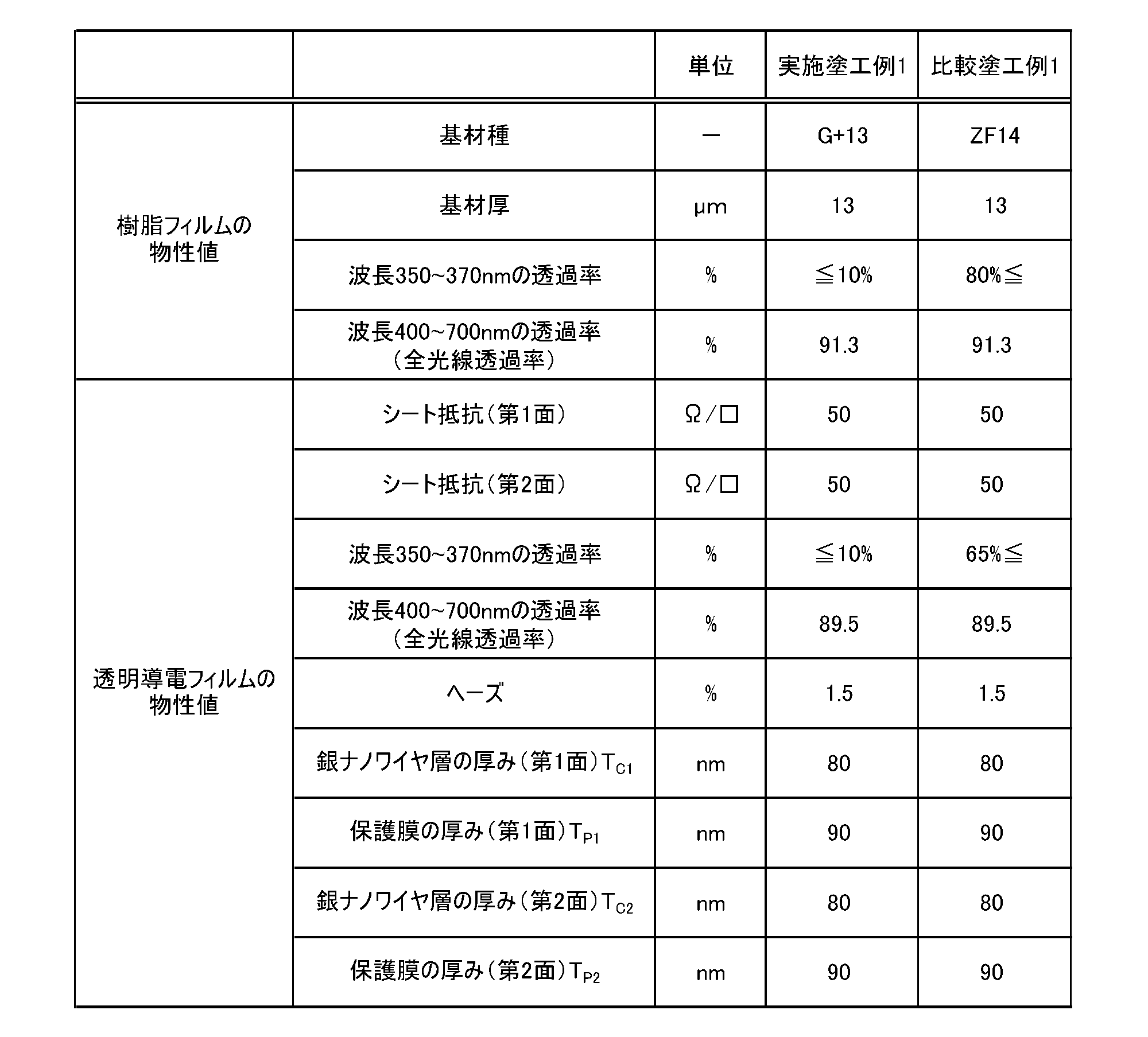
実施塗工例1で作製した透明導電フィルムの第1面に、波長355nmのフェムト秒パルスレーザー(パルス幅500fs(500×10-6ns)、周波数500kHz、加工速度4000mm/s、出力0.1W)でパターン加工を施した。加工装置は、株式会社デルファイレーザー製ULTRA PIONEERを用いた。描画したパターンは、図7に示す1辺2cmの格子パターンとした。格子内部の4ラインをまたぐようにデジタルマルチメータPC5000a(三和電気計器製)の針を当てた。パターンと針の当て方を図7に示す。図7では、上記格子を表す実線がパターン加工により形成されたエッチングラインを表しており、矢印が上記針を表している。また、α、β、γ、δは、それぞれ対応する破線で結ばれた2本の矢印(針)の先端を上記格子の内部(エッチングされていない領域)に当てて、上記エッチングラインで隔てられた二つの領域間の抵抗値を測定していることを示す。
エッチングに用いるレーザーをピコ秒パルスレーザー(パルス幅15ps(15×10-3ns)、周波数:500kHz、加工速度4000mm/s、出力0.1W)にしたこと以外は、実施加工例1と同様に測定・評価した。
エッチングに用いる透明導電フィルムを比較塗工例1のフィルムにしたこと以外は、実施加工例1と同様に測定・評価した。
エッチングに用いるレーザーをナノ秒パルスレーザー(パルス幅180ns、周波数:90kHz、加工速度500mm/s、出力0.2W)にしたこと以外は、実施加工例1と同様に測定・評価した。加工装置はESI社製Model5330を用いた。

Claims (14)
- 基材である樹脂フィルムと、
前記基材の第一の主面及び第二の主面上にそれぞれ形成された、金属ナノワイヤの交差部を有するナノ構造ネットワークとバインダー樹脂とを含む、第一の透明導電膜及び第二の透明導電膜と、
前記第一の透明導電膜及び第二の透明導電膜の上にそれぞれ形成された第一の保護膜及び第二の保護膜と、
を有し、前記樹脂フィルムはベース樹脂と紫外線吸収剤とを含み、光透過スペクトルにおいて、波長350~370nmの領域における光線透過率が10%以下であり、前記ベース樹脂の、前記樹脂フィルムと同じ厚さのフィルムの光透過スペクトルにおいて、波長350~700nmの領域における光線透過率が80%以上である、ことを特徴とする透明導電フィルム。 - 基材である樹脂フィルムの第一の主面に第一の透明導電パターン膜、第二の主面に第一の透明導電パターン膜のパターンとは異なる第二の透明導電パターン膜、をそれぞれ有し、前記第一の透明導電パターン膜上に第一の保護膜、前記第二の透明導電パターン膜上に第二の保護膜、をそれぞれ有しており、
前記第一の透明導電パターン膜が、第一の導電性領域及び第一の非導電性領域からなり、
前記第一の導電性領域が、金属ナノワイヤの交差部を有するナノ構造ネットワークとバインダー樹脂とを含み、
前記第二の透明導電パターン膜が、第二の導電性領域を含み、前記第二の導電性領域が、金属ナノワイヤの交差部を有するナノ構造ネットワークとバインダー樹脂とを含み、
前記樹脂フィルムは、ベース樹脂と紫外線吸収剤とを含み、光透過スペクトルにおいて、波長350~370nmの領域における光線透過率が10%以下であり、前記ベース樹脂の、前記樹脂フィルムと同じ厚さのフィルムの光透過スペクトルにおいて、波長350~700nmの領域における光線透過率が80%以上であることを特徴とする透明導電フィルム。 - 前記第二の透明導電パターン膜が、さらに第二の非導電性領域を含む、請求項2に記載の透明導電フィルム。
- 前記第一の非導電性領域が、金属ナノワイヤの交差部を有するナノ構造ネットワークの断片を含む、請求項2に記載の透明導電フィルム。
- 前記第二の非導電性領域が、金属ナノワイヤの交差部を有するナノ構造ネットワークの断片を含む、請求項3に記載の透明導電フィルム。
- 前記ベース樹脂が、シクロオレフィンポリマー、ポリカーボネート、ポリエステル、ポリオレフィン、ポリアラミド、アクリル樹脂、から選択される樹脂である、請求項1から5のいずれか一項に記載の透明導電フィルム。
- 前記金属ナノワイヤの交差部を有するナノ構造ネットワークが、金属ナノワイヤの交差部の少なくとも一部で融着されたものである請求項1から6のいずれか一項に記載の透明導電フィルム。
- 前記金属ナノワイヤが銀ナノワイヤである、請求項1から7のいずれか一項に記載の透明導電フィルム。
- 前記バインダー樹脂がN-ビニルアセトアミド(NVA)のホモポリマーである請求項1から8のいずれか一項に記載の透明導電フィルム。
- 前記紫外線吸収剤が、ベンゾトリアゾール系紫外線吸収剤、トリアジン系紫外線吸収剤、ベンゾフェノン系紫外線吸収剤、アクリロニトリル系紫外線吸収剤、サリチル酸系紫外線吸収剤、シアノアクリレート系紫外線吸収剤、アゾメチン系紫外線吸収剤、インドール系紫外線吸収剤、ナフタルイミド系紫外線吸収剤、フタロシアニン系紫外線吸収剤からなる群から選択される少なくとも一種である、請求項1から9のいずれか一項に記載の透明導電フィルム。
- 前記樹脂フィルムが含有する紫外線吸収剤量が、樹脂フィルムの全質量に対して0.25質量%から10質量%の範囲である、請求項1から10のいずれか一項に記載の透明導電フィルム。
- 前記第一の保護膜及び第二の保護膜が、
(A)カルボキシ基を含有するポリウレタンと、
(B)分子内に二個以上のエポキシ基を有するエポキシ化合物と、
(C)硬化促進剤と、
を含む硬化性樹脂組成物の熱硬化膜である請求項1から11のいずれか一項に記載の透明導電フィルム。 - 樹脂フィルムの第一の主面上に、金属ナノワイヤの交差部を有するナノ構造ネットワークとバインダー樹脂とを含む第一の透明導電膜、前記樹脂フィルムの第二の主面上に、金属ナノワイヤの交差部を有するナノ構造ネットワークとバインダー樹脂とを含む第二の透明導電膜、をそれぞれ形成する透明導電膜形成工程と、
前記第一の透明導電膜上に第一の保護膜、前記第二の透明導電膜上に第二の保護膜、をそれぞれ形成する保護膜形成工程と、
波長が350~370nmの範囲内であり、パルス幅が1ナノ秒より短いパルスレーザーを用いて、前記第一の保護膜側から前記第一の透明導電膜にのみエッチング加工し、第一の透明導電パターンを形成するパターン形成工程と、
を有し、
前記樹脂フィルムはベース樹脂と紫外線吸収剤とを含み、光透過スペクトルにおいて、波長350~370nmの領域における光線透過率が10%以下であり、前記ベース樹脂の、前記樹脂フィルムと同じ厚さのフィルムの光透過スペクトルにおいて、波長350~700nmの領域における光線透過率が80%以上であることを特徴とする透明導電パターンの形成方法。 - さらに、パルス幅が1ナノ秒より短いパルスレーザーを用いて、前記第二の保護膜側から前記第二の透明導電膜にのみエッチング加工し第二の透明導電パターンを形成する工程を有する請求項13に記載の透明導電パターンの形成方法。
Priority Applications (4)
| Application Number | Priority Date | Filing Date | Title |
|---|---|---|---|
| JP2023511293A JPWO2022210585A1 (ja) | 2021-03-29 | 2022-03-28 | |
| KR1020237025900A KR20230128515A (ko) | 2021-03-29 | 2022-03-28 | 투명 도전 필름 및 투명 도전 패턴의 형성 방법 |
| US18/553,303 US20240203618A1 (en) | 2021-03-29 | 2022-03-28 | Transparent conductive film and method for forming transparent conduction pattern |
| CN202280023850.6A CN117043890A (zh) | 2021-03-29 | 2022-03-28 | 透明导电薄膜及透明导电图案的形成方法 |
Applications Claiming Priority (2)
| Application Number | Priority Date | Filing Date | Title |
|---|---|---|---|
| JP2021-055394 | 2021-03-29 | ||
| JP2021055394 | 2021-03-29 |
Publications (1)
| Publication Number | Publication Date |
|---|---|
| WO2022210585A1 true WO2022210585A1 (ja) | 2022-10-06 |
Family
ID=83459298
Family Applications (1)
| Application Number | Title | Priority Date | Filing Date |
|---|---|---|---|
| PCT/JP2022/015137 Ceased WO2022210585A1 (ja) | 2021-03-29 | 2022-03-28 | 透明導電フィルム及び透明導電パターンの形成方法 |
Country Status (6)
| Country | Link |
|---|---|
| US (1) | US20240203618A1 (ja) |
| JP (1) | JPWO2022210585A1 (ja) |
| KR (1) | KR20230128515A (ja) |
| CN (1) | CN117043890A (ja) |
| TW (1) | TW202306782A (ja) |
| WO (1) | WO2022210585A1 (ja) |
Citations (7)
| Publication number | Priority date | Publication date | Assignee | Title |
|---|---|---|---|---|
| WO2009035059A1 (ja) * | 2007-09-12 | 2009-03-19 | Kuraray Co., Ltd. | 導電膜、導電部材および導電膜の製造方法 |
| JP2010244747A (ja) * | 2009-04-02 | 2010-10-28 | Konica Minolta Holdings Inc | 透明電極、透明電極の製造方法、および有機エレクトロルミネッセンス素子 |
| JP2012064498A (ja) * | 2010-09-17 | 2012-03-29 | Nagase Chemtex Corp | 透明電極基板 |
| WO2015146097A1 (ja) * | 2014-03-25 | 2015-10-01 | 凸版印刷株式会社 | 透明導電性積層体および透明導電性積層体を備えたタッチパネル |
| JP2015185512A (ja) * | 2014-03-26 | 2015-10-22 | 信越ポリマー株式会社 | 導電パターン形成基板及びその製造方法 |
| JP2016222847A (ja) * | 2015-06-02 | 2016-12-28 | 昭和電工株式会社 | 金属ナノワイヤを用いた導電パターンの保護膜用樹脂組成物及び透明導電基板 |
| WO2020174975A1 (ja) * | 2019-02-26 | 2020-09-03 | 日本ゼオン株式会社 | 積層フィルム |
Family Cites Families (3)
| Publication number | Priority date | Publication date | Assignee | Title |
|---|---|---|---|---|
| US9759846B2 (en) | 2013-09-27 | 2017-09-12 | Cam Holding Corporation | Silver nanostructure-based optical stacks and touch sensors with UV protection |
| US11154902B2 (en) | 2016-12-01 | 2021-10-26 | Showa Denko K.K. | Transparent conductive substrate and method for producing same |
| GB201803723D0 (en) | 2018-03-08 | 2018-04-25 | M Solv Ltd | Method of manufacturing a touch sensitive panel |
-
2022
- 2022-03-28 KR KR1020237025900A patent/KR20230128515A/ko active Pending
- 2022-03-28 WO PCT/JP2022/015137 patent/WO2022210585A1/ja not_active Ceased
- 2022-03-28 US US18/553,303 patent/US20240203618A1/en active Pending
- 2022-03-28 CN CN202280023850.6A patent/CN117043890A/zh active Pending
- 2022-03-28 JP JP2023511293A patent/JPWO2022210585A1/ja active Pending
- 2022-03-29 TW TW111111904A patent/TW202306782A/zh unknown
Patent Citations (7)
| Publication number | Priority date | Publication date | Assignee | Title |
|---|---|---|---|---|
| WO2009035059A1 (ja) * | 2007-09-12 | 2009-03-19 | Kuraray Co., Ltd. | 導電膜、導電部材および導電膜の製造方法 |
| JP2010244747A (ja) * | 2009-04-02 | 2010-10-28 | Konica Minolta Holdings Inc | 透明電極、透明電極の製造方法、および有機エレクトロルミネッセンス素子 |
| JP2012064498A (ja) * | 2010-09-17 | 2012-03-29 | Nagase Chemtex Corp | 透明電極基板 |
| WO2015146097A1 (ja) * | 2014-03-25 | 2015-10-01 | 凸版印刷株式会社 | 透明導電性積層体および透明導電性積層体を備えたタッチパネル |
| JP2015185512A (ja) * | 2014-03-26 | 2015-10-22 | 信越ポリマー株式会社 | 導電パターン形成基板及びその製造方法 |
| JP2016222847A (ja) * | 2015-06-02 | 2016-12-28 | 昭和電工株式会社 | 金属ナノワイヤを用いた導電パターンの保護膜用樹脂組成物及び透明導電基板 |
| WO2020174975A1 (ja) * | 2019-02-26 | 2020-09-03 | 日本ゼオン株式会社 | 積層フィルム |
Also Published As
| Publication number | Publication date |
|---|---|
| US20240203618A1 (en) | 2024-06-20 |
| KR20230128515A (ko) | 2023-09-05 |
| JPWO2022210585A1 (ja) | 2022-10-06 |
| CN117043890A (zh) | 2023-11-10 |
| TW202306782A (zh) | 2023-02-16 |
Similar Documents
| Publication | Publication Date | Title |
|---|---|---|
| KR102056658B1 (ko) | 투명 도전 기판 및 그 제조 방법 | |
| EP3988299A1 (en) | Transparent electroconductive film laminate and method for processing same | |
| JP7061734B2 (ja) | 透明導電フィルム積層体及びその加工方法 | |
| KR102387063B1 (ko) | 투명 도전 필름의 제조 방법 | |
| US20220139591A1 (en) | Transparent conductive film, and touch panel including same | |
| JP7435831B2 (ja) | 透明導電フィルム積層体 | |
| US20240203618A1 (en) | Transparent conductive film and method for forming transparent conduction pattern | |
| WO2022210586A1 (ja) | 透明導電フィルム及び透明導電パターンの形成方法 | |
| WO2021131099A1 (ja) | 透明導電フィルムの製造方法 | |
| JP2023095255A (ja) | ヒータ | |
| US11685846B2 (en) | Transparent conducting film | |
| JP2023095223A (ja) | タッチセンサ及びタッチセンサを備えた器具 | |
| JP2023095412A (ja) | 加飾タッチパネル及びタッチパネル内蔵ディスプレイ | |
| JP2024067269A (ja) | 透明導電フィルム積層体及びその製造方法並びに成形用透明導電フィルム積層体 | |
| WO2023120620A1 (ja) | タッチパネル及びタッチパネルの製造方法 | |
| WO2023286602A1 (ja) | 透明導電フィルム積層体及びその製造方法 | |
| CN112970075B (zh) | 透明导电膜的制造方法 | |
| WO2023286601A1 (ja) | 透明導電フィルム積層体及びその製造方法 |
Legal Events
| Date | Code | Title | Description |
|---|---|---|---|
| 121 | Ep: the epo has been informed by wipo that ep was designated in this application |
Ref document number: 22780796 Country of ref document: EP Kind code of ref document: A1 |
|
| ENP | Entry into the national phase |
Ref document number: 2023511293 Country of ref document: JP Kind code of ref document: A |
|
| ENP | Entry into the national phase |
Ref document number: 20237025900 Country of ref document: KR Kind code of ref document: A |
|
| WWE | Wipo information: entry into national phase |
Ref document number: 202280023850.6 Country of ref document: CN |
|
| WWE | Wipo information: entry into national phase |
Ref document number: 2301006319 Country of ref document: TH |
|
| WWE | Wipo information: entry into national phase |
Ref document number: 18553303 Country of ref document: US |
|
| NENP | Non-entry into the national phase |
Ref country code: DE |
|
| 122 | Ep: pct application non-entry in european phase |
Ref document number: 22780796 Country of ref document: EP Kind code of ref document: A1 |