WO2022210401A1 - Laminated structure - Google Patents
Laminated structure Download PDFInfo
- Publication number
- WO2022210401A1 WO2022210401A1 PCT/JP2022/014563 JP2022014563W WO2022210401A1 WO 2022210401 A1 WO2022210401 A1 WO 2022210401A1 JP 2022014563 W JP2022014563 W JP 2022014563W WO 2022210401 A1 WO2022210401 A1 WO 2022210401A1
- Authority
- WO
- WIPO (PCT)
- Prior art keywords
- layer
- substrate
- laminated structure
- gallium nitride
- nitride film
- Prior art date
Links
- 239000010410 layer Substances 0.000 claims abstract description 213
- 229910002601 GaN Inorganic materials 0.000 claims abstract description 150
- JMASRVWKEDWRBT-UHFFFAOYSA-N Gallium nitride Chemical compound [Ga]#N JMASRVWKEDWRBT-UHFFFAOYSA-N 0.000 claims abstract description 126
- 239000000758 substrate Substances 0.000 claims abstract description 122
- 239000011241 protective layer Substances 0.000 claims abstract description 44
- 239000010936 titanium Substances 0.000 claims description 10
- 239000011521 glass Substances 0.000 claims description 9
- RTAQQCXQSZGOHL-UHFFFAOYSA-N Titanium Chemical group [Ti] RTAQQCXQSZGOHL-UHFFFAOYSA-N 0.000 claims description 8
- 229910052719 titanium Inorganic materials 0.000 claims description 8
- PXHVJJICTQNCMI-UHFFFAOYSA-N Nickel Chemical compound [Ni] PXHVJJICTQNCMI-UHFFFAOYSA-N 0.000 claims description 7
- KDLHZDBZIXYQEI-UHFFFAOYSA-N Palladium Chemical compound [Pd] KDLHZDBZIXYQEI-UHFFFAOYSA-N 0.000 claims description 7
- 229910052814 silicon oxide Inorganic materials 0.000 claims description 7
- 229910052581 Si3N4 Inorganic materials 0.000 claims description 6
- VYPSYNLAJGMNEJ-UHFFFAOYSA-N Silicium dioxide Chemical compound O=[Si]=O VYPSYNLAJGMNEJ-UHFFFAOYSA-N 0.000 claims description 6
- HQVNEWCFYHHQES-UHFFFAOYSA-N silicon nitride Chemical compound N12[Si]34N5[Si]62N3[Si]51N64 HQVNEWCFYHHQES-UHFFFAOYSA-N 0.000 claims description 6
- XLOMVQKBTHCTTD-UHFFFAOYSA-N Zinc monoxide Chemical compound [Zn]=O XLOMVQKBTHCTTD-UHFFFAOYSA-N 0.000 claims description 5
- 239000004020 conductor Substances 0.000 claims description 5
- 239000010931 gold Substances 0.000 claims description 5
- BASFCYQUMIYNBI-UHFFFAOYSA-N platinum Chemical compound [Pt] BASFCYQUMIYNBI-UHFFFAOYSA-N 0.000 claims description 5
- 239000011347 resin Substances 0.000 claims description 5
- 229920005989 resin Polymers 0.000 claims description 5
- 229910052782 aluminium Inorganic materials 0.000 claims description 4
- XAGFODPZIPBFFR-UHFFFAOYSA-N aluminium Chemical compound [Al] XAGFODPZIPBFFR-UHFFFAOYSA-N 0.000 claims description 4
- PMHQVHHXPFUNSP-UHFFFAOYSA-M copper(1+);methylsulfanylmethane;bromide Chemical compound Br[Cu].CSC PMHQVHHXPFUNSP-UHFFFAOYSA-M 0.000 claims description 4
- PCHJSUWPFVWCPO-UHFFFAOYSA-N gold Chemical compound [Au] PCHJSUWPFVWCPO-UHFFFAOYSA-N 0.000 claims description 4
- 229910052737 gold Inorganic materials 0.000 claims description 4
- OGIDPMRJRNCKJF-UHFFFAOYSA-N titanium oxide Inorganic materials [Ti]=O OGIDPMRJRNCKJF-UHFFFAOYSA-N 0.000 claims description 4
- OKTJSMMVPCPJKN-UHFFFAOYSA-N Carbon Chemical compound [C] OKTJSMMVPCPJKN-UHFFFAOYSA-N 0.000 claims description 3
- GWEVSGVZZGPLCZ-UHFFFAOYSA-N Titan oxide Chemical compound O=[Ti]=O GWEVSGVZZGPLCZ-UHFFFAOYSA-N 0.000 claims description 3
- NRTOMJZYCJJWKI-UHFFFAOYSA-N Titanium nitride Chemical compound [Ti]#N NRTOMJZYCJJWKI-UHFFFAOYSA-N 0.000 claims description 3
- 239000011575 calcium Substances 0.000 claims description 3
- 239000010949 copper Substances 0.000 claims description 3
- 229910021389 graphene Inorganic materials 0.000 claims description 3
- 239000012212 insulator Substances 0.000 claims description 3
- 239000011133 lead Substances 0.000 claims description 3
- 229910052759 nickel Inorganic materials 0.000 claims description 3
- TWNQGVIAIRXVLR-UHFFFAOYSA-N oxo(oxoalumanyloxy)alumane Chemical compound O=[Al]O[Al]=O TWNQGVIAIRXVLR-UHFFFAOYSA-N 0.000 claims description 3
- 229910052763 palladium Inorganic materials 0.000 claims description 3
- 239000010948 rhodium Substances 0.000 claims description 3
- ZSLUVFAKFWKJRC-IGMARMGPSA-N 232Th Chemical compound [232Th] ZSLUVFAKFWKJRC-IGMARMGPSA-N 0.000 claims description 2
- OYPRJOBELJOOCE-UHFFFAOYSA-N Calcium Chemical compound [Ca] OYPRJOBELJOOCE-UHFFFAOYSA-N 0.000 claims description 2
- 229910052684 Cerium Inorganic materials 0.000 claims description 2
- RYGMFSIKBFXOCR-UHFFFAOYSA-N Copper Chemical compound [Cu] RYGMFSIKBFXOCR-UHFFFAOYSA-N 0.000 claims description 2
- BQCADISMDOOEFD-UHFFFAOYSA-N Silver Chemical compound [Ag] BQCADISMDOOEFD-UHFFFAOYSA-N 0.000 claims description 2
- 229910052776 Thorium Inorganic materials 0.000 claims description 2
- 229910052769 Ytterbium Inorganic materials 0.000 claims description 2
- PZKRHHZKOQZHIO-UHFFFAOYSA-N [B].[B].[Mg] Chemical compound [B].[B].[Mg] PZKRHHZKOQZHIO-UHFFFAOYSA-N 0.000 claims description 2
- 229910052767 actinium Inorganic materials 0.000 claims description 2
- QQINRWTZWGJFDB-UHFFFAOYSA-N actinium atom Chemical compound [Ac] QQINRWTZWGJFDB-UHFFFAOYSA-N 0.000 claims description 2
- 229910052791 calcium Inorganic materials 0.000 claims description 2
- GWXLDORMOJMVQZ-UHFFFAOYSA-N cerium Chemical compound [Ce] GWXLDORMOJMVQZ-UHFFFAOYSA-N 0.000 claims description 2
- 229910052802 copper Inorganic materials 0.000 claims description 2
- 229910052741 iridium Inorganic materials 0.000 claims description 2
- GKOZUEZYRPOHIO-UHFFFAOYSA-N iridium atom Chemical compound [Ir] GKOZUEZYRPOHIO-UHFFFAOYSA-N 0.000 claims description 2
- GQYHUHYESMUTHG-UHFFFAOYSA-N lithium niobate Chemical compound [Li+].[O-][Nb](=O)=O GQYHUHYESMUTHG-UHFFFAOYSA-N 0.000 claims description 2
- 229910052697 platinum Inorganic materials 0.000 claims description 2
- 229910052703 rhodium Inorganic materials 0.000 claims description 2
- MHOVAHRLVXNVSD-UHFFFAOYSA-N rhodium atom Chemical compound [Rh] MHOVAHRLVXNVSD-UHFFFAOYSA-N 0.000 claims description 2
- 229910052709 silver Inorganic materials 0.000 claims description 2
- 239000004332 silver Substances 0.000 claims description 2
- 229910052712 strontium Inorganic materials 0.000 claims description 2
- CIOAGBVUUVVLOB-UHFFFAOYSA-N strontium atom Chemical compound [Sr] CIOAGBVUUVVLOB-UHFFFAOYSA-N 0.000 claims description 2
- NAWDYIZEMPQZHO-UHFFFAOYSA-N ytterbium Chemical compound [Yb] NAWDYIZEMPQZHO-UHFFFAOYSA-N 0.000 claims description 2
- 239000011787 zinc oxide Substances 0.000 claims description 2
- RNQKDQAVIXDKAG-UHFFFAOYSA-N aluminum gallium Chemical compound [Al].[Ga] RNQKDQAVIXDKAG-UHFFFAOYSA-N 0.000 description 25
- 238000010586 diagram Methods 0.000 description 24
- 239000004065 semiconductor Substances 0.000 description 20
- 238000004544 sputter deposition Methods 0.000 description 14
- 239000013078 crystal Substances 0.000 description 13
- 235000019592 roughness Nutrition 0.000 description 11
- 239000000463 material Substances 0.000 description 9
- 238000000059 patterning Methods 0.000 description 9
- IJGRMHOSHXDMSA-UHFFFAOYSA-N Atomic nitrogen Chemical compound N#N IJGRMHOSHXDMSA-UHFFFAOYSA-N 0.000 description 8
- 238000012986 modification Methods 0.000 description 8
- 230000004048 modification Effects 0.000 description 8
- 238000000206 photolithography Methods 0.000 description 7
- 230000003746 surface roughness Effects 0.000 description 7
- 229910052751 metal Inorganic materials 0.000 description 6
- 239000002184 metal Substances 0.000 description 6
- 229910052738 indium Inorganic materials 0.000 description 5
- APFVFJFRJDLVQX-UHFFFAOYSA-N indium atom Chemical compound [In] APFVFJFRJDLVQX-UHFFFAOYSA-N 0.000 description 5
- LIVNPJMFVYWSIS-UHFFFAOYSA-N silicon monoxide Chemical compound [Si-]#[O+] LIVNPJMFVYWSIS-UHFFFAOYSA-N 0.000 description 5
- 238000004519 manufacturing process Methods 0.000 description 4
- 229910052757 nitrogen Inorganic materials 0.000 description 4
- GYHNNYVSQQEPJS-UHFFFAOYSA-N Gallium Chemical compound [Ga] GYHNNYVSQQEPJS-UHFFFAOYSA-N 0.000 description 3
- 238000000151 deposition Methods 0.000 description 3
- 230000008021 deposition Effects 0.000 description 3
- 229910052733 gallium Inorganic materials 0.000 description 3
- 230000014509 gene expression Effects 0.000 description 3
- 238000002248 hydride vapour-phase epitaxy Methods 0.000 description 3
- 239000012535 impurity Substances 0.000 description 3
- 229910052594 sapphire Inorganic materials 0.000 description 3
- 239000010980 sapphire Substances 0.000 description 3
- XKRFYHLGVUSROY-UHFFFAOYSA-N Argon Chemical compound [Ar] XKRFYHLGVUSROY-UHFFFAOYSA-N 0.000 description 2
- 230000015572 biosynthetic process Effects 0.000 description 2
- 230000000694 effects Effects 0.000 description 2
- 238000005530 etching Methods 0.000 description 2
- 238000000605 extraction Methods 0.000 description 2
- 239000007789 gas Substances 0.000 description 2
- 238000000034 method Methods 0.000 description 2
- 239000000203 mixture Substances 0.000 description 2
- 239000004642 Polyimide Substances 0.000 description 1
- ATJFFYVFTNAWJD-UHFFFAOYSA-N Tin Chemical compound [Sn] ATJFFYVFTNAWJD-UHFFFAOYSA-N 0.000 description 1
- NIXOWILDQLNWCW-UHFFFAOYSA-N acrylic acid group Chemical group C(C=C)(=O)O NIXOWILDQLNWCW-UHFFFAOYSA-N 0.000 description 1
- PNEYBMLMFCGWSK-UHFFFAOYSA-N aluminium oxide Inorganic materials [O-2].[O-2].[O-2].[Al+3].[Al+3] PNEYBMLMFCGWSK-UHFFFAOYSA-N 0.000 description 1
- 229910052586 apatite Inorganic materials 0.000 description 1
- 229910052786 argon Inorganic materials 0.000 description 1
- 230000000035 biogenic effect Effects 0.000 description 1
- 230000015556 catabolic process Effects 0.000 description 1
- 238000005229 chemical vapour deposition Methods 0.000 description 1
- 229910052593 corundum Inorganic materials 0.000 description 1
- 238000013461 design Methods 0.000 description 1
- 238000011161 development Methods 0.000 description 1
- 238000009792 diffusion process Methods 0.000 description 1
- KPUWHANPEXNPJT-UHFFFAOYSA-N disiloxane Chemical class [SiH3]O[SiH3] KPUWHANPEXNPJT-UHFFFAOYSA-N 0.000 description 1
- 230000002401 inhibitory effect Effects 0.000 description 1
- 229910052743 krypton Inorganic materials 0.000 description 1
- DNNSSWSSYDEUBZ-UHFFFAOYSA-N krypton atom Chemical compound [Kr] DNNSSWSSYDEUBZ-UHFFFAOYSA-N 0.000 description 1
- QJGQUHMNIGDVPM-UHFFFAOYSA-N nitrogen(.) Chemical compound [N] QJGQUHMNIGDVPM-UHFFFAOYSA-N 0.000 description 1
- VSIIXMUUUJUKCM-UHFFFAOYSA-D pentacalcium;fluoride;triphosphate Chemical compound [F-].[Ca+2].[Ca+2].[Ca+2].[Ca+2].[Ca+2].[O-]P([O-])([O-])=O.[O-]P([O-])([O-])=O.[O-]P([O-])([O-])=O VSIIXMUUUJUKCM-UHFFFAOYSA-D 0.000 description 1
- 229910021420 polycrystalline silicon Inorganic materials 0.000 description 1
- 229920001721 polyimide Polymers 0.000 description 1
- 229920005591 polysilicon Polymers 0.000 description 1
- 238000009751 slip forming Methods 0.000 description 1
- 238000012546 transfer Methods 0.000 description 1
- 229910001845 yogo sapphire Inorganic materials 0.000 description 1
Images


Classifications
-
- H—ELECTRICITY
- H01—ELECTRIC ELEMENTS
- H01L—SEMICONDUCTOR DEVICES NOT COVERED BY CLASS H10
- H01L33/00—Semiconductor devices with at least one potential-jump barrier or surface barrier specially adapted for light emission; Processes or apparatus specially adapted for the manufacture or treatment thereof or of parts thereof; Details thereof
- H01L33/02—Semiconductor devices with at least one potential-jump barrier or surface barrier specially adapted for light emission; Processes or apparatus specially adapted for the manufacture or treatment thereof or of parts thereof; Details thereof characterised by the semiconductor bodies
- H01L33/26—Materials of the light emitting region
- H01L33/30—Materials of the light emitting region containing only elements of group III and group V of the periodic system
- H01L33/32—Materials of the light emitting region containing only elements of group III and group V of the periodic system containing nitrogen
- H01L33/325—Materials of the light emitting region containing only elements of group III and group V of the periodic system containing nitrogen characterised by the doping materials
-
- C—CHEMISTRY; METALLURGY
- C23—COATING METALLIC MATERIAL; COATING MATERIAL WITH METALLIC MATERIAL; CHEMICAL SURFACE TREATMENT; DIFFUSION TREATMENT OF METALLIC MATERIAL; COATING BY VACUUM EVAPORATION, BY SPUTTERING, BY ION IMPLANTATION OR BY CHEMICAL VAPOUR DEPOSITION, IN GENERAL; INHIBITING CORROSION OF METALLIC MATERIAL OR INCRUSTATION IN GENERAL
- C23C—COATING METALLIC MATERIAL; COATING MATERIAL WITH METALLIC MATERIAL; SURFACE TREATMENT OF METALLIC MATERIAL BY DIFFUSION INTO THE SURFACE, BY CHEMICAL CONVERSION OR SUBSTITUTION; COATING BY VACUUM EVAPORATION, BY SPUTTERING, BY ION IMPLANTATION OR BY CHEMICAL VAPOUR DEPOSITION, IN GENERAL
- C23C14/00—Coating by vacuum evaporation, by sputtering or by ion implantation of the coating forming material
- C23C14/06—Coating by vacuum evaporation, by sputtering or by ion implantation of the coating forming material characterised by the coating material
- C23C14/0641—Nitrides
-
- C—CHEMISTRY; METALLURGY
- C30—CRYSTAL GROWTH
- C30B—SINGLE-CRYSTAL GROWTH; UNIDIRECTIONAL SOLIDIFICATION OF EUTECTIC MATERIAL OR UNIDIRECTIONAL DEMIXING OF EUTECTOID MATERIAL; REFINING BY ZONE-MELTING OF MATERIAL; PRODUCTION OF A HOMOGENEOUS POLYCRYSTALLINE MATERIAL WITH DEFINED STRUCTURE; SINGLE CRYSTALS OR HOMOGENEOUS POLYCRYSTALLINE MATERIAL WITH DEFINED STRUCTURE; AFTER-TREATMENT OF SINGLE CRYSTALS OR A HOMOGENEOUS POLYCRYSTALLINE MATERIAL WITH DEFINED STRUCTURE; APPARATUS THEREFOR
- C30B23/00—Single-crystal growth by condensing evaporated or sublimed materials
- C30B23/02—Epitaxial-layer growth
- C30B23/025—Epitaxial-layer growth characterised by the substrate
-
- C—CHEMISTRY; METALLURGY
- C30—CRYSTAL GROWTH
- C30B—SINGLE-CRYSTAL GROWTH; UNIDIRECTIONAL SOLIDIFICATION OF EUTECTIC MATERIAL OR UNIDIRECTIONAL DEMIXING OF EUTECTOID MATERIAL; REFINING BY ZONE-MELTING OF MATERIAL; PRODUCTION OF A HOMOGENEOUS POLYCRYSTALLINE MATERIAL WITH DEFINED STRUCTURE; SINGLE CRYSTALS OR HOMOGENEOUS POLYCRYSTALLINE MATERIAL WITH DEFINED STRUCTURE; AFTER-TREATMENT OF SINGLE CRYSTALS OR A HOMOGENEOUS POLYCRYSTALLINE MATERIAL WITH DEFINED STRUCTURE; APPARATUS THEREFOR
- C30B29/00—Single crystals or homogeneous polycrystalline material with defined structure characterised by the material or by their shape
- C30B29/10—Inorganic compounds or compositions
- C30B29/40—AIIIBV compounds wherein A is B, Al, Ga, In or Tl and B is N, P, As, Sb or Bi
- C30B29/403—AIII-nitrides
- C30B29/406—Gallium nitride
-
- H—ELECTRICITY
- H01—ELECTRIC ELEMENTS
- H01L—SEMICONDUCTOR DEVICES NOT COVERED BY CLASS H10
- H01L21/00—Processes or apparatus adapted for the manufacture or treatment of semiconductor or solid state devices or of parts thereof
- H01L21/02—Manufacture or treatment of semiconductor devices or of parts thereof
-
- H—ELECTRICITY
- H01—ELECTRIC ELEMENTS
- H01L—SEMICONDUCTOR DEVICES NOT COVERED BY CLASS H10
- H01L29/00—Semiconductor devices adapted for rectifying, amplifying, oscillating or switching, or capacitors or resistors with at least one potential-jump barrier or surface barrier, e.g. PN junction depletion layer or carrier concentration layer; Details of semiconductor bodies or of electrodes thereof ; Multistep manufacturing processes therefor
- H01L29/02—Semiconductor bodies ; Multistep manufacturing processes therefor
- H01L29/06—Semiconductor bodies ; Multistep manufacturing processes therefor characterised by their shape; characterised by the shapes, relative sizes, or dispositions of the semiconductor regions ; characterised by the concentration or distribution of impurities within semiconductor regions
- H01L29/10—Semiconductor bodies ; Multistep manufacturing processes therefor characterised by their shape; characterised by the shapes, relative sizes, or dispositions of the semiconductor regions ; characterised by the concentration or distribution of impurities within semiconductor regions with semiconductor regions connected to an electrode not carrying current to be rectified, amplified or switched and such electrode being part of a semiconductor device which comprises three or more electrodes
-
- H—ELECTRICITY
- H01—ELECTRIC ELEMENTS
- H01L—SEMICONDUCTOR DEVICES NOT COVERED BY CLASS H10
- H01L29/00—Semiconductor devices adapted for rectifying, amplifying, oscillating or switching, or capacitors or resistors with at least one potential-jump barrier or surface barrier, e.g. PN junction depletion layer or carrier concentration layer; Details of semiconductor bodies or of electrodes thereof ; Multistep manufacturing processes therefor
- H01L29/02—Semiconductor bodies ; Multistep manufacturing processes therefor
- H01L29/12—Semiconductor bodies ; Multistep manufacturing processes therefor characterised by the materials of which they are formed
- H01L29/20—Semiconductor bodies ; Multistep manufacturing processes therefor characterised by the materials of which they are formed including, apart from doping materials or other impurities, only AIIIBV compounds
- H01L29/201—Semiconductor bodies ; Multistep manufacturing processes therefor characterised by the materials of which they are formed including, apart from doping materials or other impurities, only AIIIBV compounds including two or more compounds, e.g. alloys
-
- H—ELECTRICITY
- H01—ELECTRIC ELEMENTS
- H01L—SEMICONDUCTOR DEVICES NOT COVERED BY CLASS H10
- H01L29/00—Semiconductor devices adapted for rectifying, amplifying, oscillating or switching, or capacitors or resistors with at least one potential-jump barrier or surface barrier, e.g. PN junction depletion layer or carrier concentration layer; Details of semiconductor bodies or of electrodes thereof ; Multistep manufacturing processes therefor
- H01L29/66—Types of semiconductor device ; Multistep manufacturing processes therefor
- H01L29/66007—Multistep manufacturing processes
- H01L29/66075—Multistep manufacturing processes of devices having semiconductor bodies comprising group 14 or group 13/15 materials
- H01L29/66227—Multistep manufacturing processes of devices having semiconductor bodies comprising group 14 or group 13/15 materials the devices being controllable only by the electric current supplied or the electric potential applied, to an electrode which does not carry the current to be rectified, amplified or switched, e.g. three-terminal devices
- H01L29/66409—Unipolar field-effect transistors
- H01L29/66477—Unipolar field-effect transistors with an insulated gate, i.e. MISFET
-
- H—ELECTRICITY
- H01—ELECTRIC ELEMENTS
- H01L—SEMICONDUCTOR DEVICES NOT COVERED BY CLASS H10
- H01L29/00—Semiconductor devices adapted for rectifying, amplifying, oscillating or switching, or capacitors or resistors with at least one potential-jump barrier or surface barrier, e.g. PN junction depletion layer or carrier concentration layer; Details of semiconductor bodies or of electrodes thereof ; Multistep manufacturing processes therefor
- H01L29/66—Types of semiconductor device ; Multistep manufacturing processes therefor
- H01L29/66007—Multistep manufacturing processes
- H01L29/66075—Multistep manufacturing processes of devices having semiconductor bodies comprising group 14 or group 13/15 materials
- H01L29/66227—Multistep manufacturing processes of devices having semiconductor bodies comprising group 14 or group 13/15 materials the devices being controllable only by the electric current supplied or the electric potential applied, to an electrode which does not carry the current to be rectified, amplified or switched, e.g. three-terminal devices
- H01L29/66409—Unipolar field-effect transistors
- H01L29/66848—Unipolar field-effect transistors with a Schottky gate, i.e. MESFET
-
- H—ELECTRICITY
- H01—ELECTRIC ELEMENTS
- H01L—SEMICONDUCTOR DEVICES NOT COVERED BY CLASS H10
- H01L29/00—Semiconductor devices adapted for rectifying, amplifying, oscillating or switching, or capacitors or resistors with at least one potential-jump barrier or surface barrier, e.g. PN junction depletion layer or carrier concentration layer; Details of semiconductor bodies or of electrodes thereof ; Multistep manufacturing processes therefor
- H01L29/66—Types of semiconductor device ; Multistep manufacturing processes therefor
- H01L29/68—Types of semiconductor device ; Multistep manufacturing processes therefor controllable by only the electric current supplied, or only the electric potential applied, to an electrode which does not carry the current to be rectified, amplified or switched
- H01L29/76—Unipolar devices, e.g. field effect transistors
- H01L29/772—Field effect transistors
- H01L29/778—Field effect transistors with two-dimensional charge carrier gas channel, e.g. HEMT ; with two-dimensional charge-carrier layer formed at a heterojunction interface
-
- H—ELECTRICITY
- H01—ELECTRIC ELEMENTS
- H01L—SEMICONDUCTOR DEVICES NOT COVERED BY CLASS H10
- H01L29/00—Semiconductor devices adapted for rectifying, amplifying, oscillating or switching, or capacitors or resistors with at least one potential-jump barrier or surface barrier, e.g. PN junction depletion layer or carrier concentration layer; Details of semiconductor bodies or of electrodes thereof ; Multistep manufacturing processes therefor
- H01L29/66—Types of semiconductor device ; Multistep manufacturing processes therefor
- H01L29/68—Types of semiconductor device ; Multistep manufacturing processes therefor controllable by only the electric current supplied, or only the electric potential applied, to an electrode which does not carry the current to be rectified, amplified or switched
- H01L29/76—Unipolar devices, e.g. field effect transistors
- H01L29/772—Field effect transistors
- H01L29/78—Field effect transistors with field effect produced by an insulated gate
- H01L29/786—Thin film transistors, i.e. transistors with a channel being at least partly a thin film
-
- H—ELECTRICITY
- H01—ELECTRIC ELEMENTS
- H01L—SEMICONDUCTOR DEVICES NOT COVERED BY CLASS H10
- H01L29/00—Semiconductor devices adapted for rectifying, amplifying, oscillating or switching, or capacitors or resistors with at least one potential-jump barrier or surface barrier, e.g. PN junction depletion layer or carrier concentration layer; Details of semiconductor bodies or of electrodes thereof ; Multistep manufacturing processes therefor
- H01L29/66—Types of semiconductor device ; Multistep manufacturing processes therefor
- H01L29/68—Types of semiconductor device ; Multistep manufacturing processes therefor controllable by only the electric current supplied, or only the electric potential applied, to an electrode which does not carry the current to be rectified, amplified or switched
- H01L29/76—Unipolar devices, e.g. field effect transistors
- H01L29/772—Field effect transistors
- H01L29/80—Field effect transistors with field effect produced by a PN or other rectifying junction gate, i.e. potential-jump barrier
- H01L29/812—Field effect transistors with field effect produced by a PN or other rectifying junction gate, i.e. potential-jump barrier with a Schottky gate
-
- H—ELECTRICITY
- H01—ELECTRIC ELEMENTS
- H01L—SEMICONDUCTOR DEVICES NOT COVERED BY CLASS H10
- H01L33/00—Semiconductor devices with at least one potential-jump barrier or surface barrier specially adapted for light emission; Processes or apparatus specially adapted for the manufacture or treatment thereof or of parts thereof; Details thereof
- H01L33/02—Semiconductor devices with at least one potential-jump barrier or surface barrier specially adapted for light emission; Processes or apparatus specially adapted for the manufacture or treatment thereof or of parts thereof; Details thereof characterised by the semiconductor bodies
- H01L33/20—Semiconductor devices with at least one potential-jump barrier or surface barrier specially adapted for light emission; Processes or apparatus specially adapted for the manufacture or treatment thereof or of parts thereof; Details thereof characterised by the semiconductor bodies with a particular shape, e.g. curved or truncated substrate
- H01L33/22—Roughened surfaces, e.g. at the interface between epitaxial layers
-
- H—ELECTRICITY
- H01—ELECTRIC ELEMENTS
- H01L—SEMICONDUCTOR DEVICES NOT COVERED BY CLASS H10
- H01L33/00—Semiconductor devices with at least one potential-jump barrier or surface barrier specially adapted for light emission; Processes or apparatus specially adapted for the manufacture or treatment thereof or of parts thereof; Details thereof
- H01L33/02—Semiconductor devices with at least one potential-jump barrier or surface barrier specially adapted for light emission; Processes or apparatus specially adapted for the manufacture or treatment thereof or of parts thereof; Details thereof characterised by the semiconductor bodies
- H01L33/20—Semiconductor devices with at least one potential-jump barrier or surface barrier specially adapted for light emission; Processes or apparatus specially adapted for the manufacture or treatment thereof or of parts thereof; Details thereof characterised by the semiconductor bodies with a particular shape, e.g. curved or truncated substrate
Definitions
- One embodiment of the present invention relates to a laminated structure including a gallium nitride film formed on a substrate.
- Gallium nitride is characterized as a direct bandgap semiconductor with a large bandgap. Taking advantage of this feature of gallium nitride, light-emitting diodes (LEDs) using gallium nitride have already been put to practical use. In addition, gallium nitride also has the characteristics of high electron saturation mobility and high breakdown voltage. In recent years, utilizing the characteristics of gallium nitride, the development of transistors for high-frequency power devices is underway. Gallium nitride films for light-emitting diodes or transistors are generally formed on sapphire substrates at high temperatures of 800° C. to 1000° C. using MOCVD (Metal Organic Chemical Vapor Deposition) or HVPE (Hydride Vapor Phase Epitaxy).
- MOCVD Metal Organic Chemical Vapor Deposition
- HVPE Hydride Vapor Phase Epitaxy
- Micro LED display or mini LED display has high efficiency, high brightness and high reliability.
- Such a micro-LED display device or mini-LED display device is manufactured by transferring an LED chip to a backplane on which a transistor using an oxide semiconductor or low-temperature polysilicon is formed (see, for example, Patent Documents 1). Further, a method of forming a transistor containing gallium nitride and a light-emitting diode over the same substrate has also been studied (see Patent Document 2, for example).
- gallium nitride films are generally formed on sapphire substrates at high temperatures.
- a large-area substrate such as an amorphous glass substrate has low heat resistance, and a gallium nitride film formed at a low temperature has a problem of low crystallinity.
- Another problem is that it is difficult to provide a large-area backplane.
- one object of an embodiment of the present invention is to provide a laminated structure in which a highly crystalline gallium nitride film is formed on a substrate that can be increased in area.
- a laminated structure according to one embodiment of the present invention includes a substrate and a gallium nitride film on the substrate, and the surface arithmetic mean roughness (Ra) of the substrate is less than 0.33 nm.
- a laminated structure according to one embodiment of the present invention includes a substrate, an orientation layer having c-axis orientation or face-centered cubic (111) orientation on the substrate, and a gallium nitride film on the orientation layer,
- the surface arithmetic mean roughness (Ra) of the substrate is less than 0.33 nm.
- a laminated structure includes a substrate, a protective layer on the substrate, an orientation layer having c-axis orientation or face-centered cubic (111) orientation on the protective layer, and and a gallium nitride film, and the surface arithmetic mean roughness (Ra) of the substrate is less than 0.33 nm.
- FIG. 1 is a schematic diagram showing the configuration of a laminated structure according to one embodiment of the present invention
- FIG. 1 is a schematic diagram showing the configuration of a laminated structure according to one embodiment of the present invention
- FIG. 1 is a schematic diagram showing the configuration of a laminated structure according to one embodiment of the present invention
- FIG. 1 is a schematic diagram showing the configuration of a laminated structure according to one embodiment of the present invention
- FIG. 1 is a schematic diagram showing the configuration of a laminated structure according to one embodiment of the present invention
- FIG. 1 is a schematic diagram showing the configuration of a laminated structure according to one embodiment of the present invention
- FIG. 1 is a schematic diagram showing the configuration of a laminated structure according to one embodiment of the present invention
- FIG. 1 is a schematic diagram showing the configuration of a laminated structure according to one embodiment of the present invention
- FIG. 1 is a schematic diagram showing the configuration of a laminated structure according to one embodiment of the present invention
- FIG. 1 is a schematic diagram showing the configuration of a laminated structure according to one embodiment of the present invention
- FIG. 1 is a schematic diagram showing the configuration of a laminated structure according to one embodiment of the present invention
- FIG. 1 is a schematic diagram showing the configuration of a light-emitting device using a laminated structure according to one embodiment of the present invention
- FIG. 1 is a schematic diagram showing the configuration of a semiconductor device using a laminated structure according to one embodiment of the present invention
- ⁇ includes A, B or C
- ⁇ includes any one of A, B and C
- ⁇ includes one selected from the group consisting of A, B and C
- ⁇ does not exclude the case where ⁇ includes a plurality of combinations of A to C, unless otherwise specified.
- these expressions do not exclude the case where ⁇ contains other elements.
- the terms “upper”, “upper”, “lower”, and “lower” are used, but in principle, the substrate on which the structure is formed is used as a reference, and the structure is formed from the substrate. Let the direction toward an object be “up” or “upper”. Conversely, the direction from the structure toward the substrate is defined as “down” or “lower”. Therefore, in the expression of the structure on the substrate, the surface of the structure facing the substrate is the lower surface of the structure, and the opposite surface is the upper surface of the structure.
- the expression “structure on the substrate” merely describes the vertical relationship between the substrate and the structure, and other members may be arranged between the substrate and the structure.
- the terms “upper” or “upper” or “lower” or “lower” mean the order of stacking in a structure in which a plurality of layers are stacked, even if they are not in an overlapping positional relationship in plan view. good.
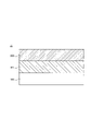
- FIG. 1 is a schematic diagram showing the configuration of a laminated structure according to one embodiment of the present invention.
- a laminated structure 10 includes a substrate 100 and a gallium nitride film 200 .
- a gallium nitride film 200 is formed on the substrate 100 using sputtering.
- the substrate 100 is a support substrate for the gallium nitride film 200 . Since the gallium nitride film 200 of the laminated structure 10 is formed by sputtering, the substrate 100 may have heat resistance of about 600° C., for example. Therefore, for example, an amorphous glass substrate can be used as the substrate 100 .
- a resin substrate such as a polyimide substrate, an acrylic substrate, a siloxane substrate, or a fluororesin substrate can be used as the substrate 100 .
- a resin substrate such as a polyimide substrate, an acrylic substrate, a siloxane substrate, or a fluororesin substrate can be used. Note that an amorphous glass substrate or a resin substrate is a substrate that can have a large area.
- a polycrystalline substrate can also be used as the substrate 100 . Since the polycrystalline substrate is larger than the sapphire substrate used in normal film formation of gallium nitride films, it can be used as a backplane in the same manner as
- the crystal growth of the gallium nitride film 200 on the substrate 100 such as amorphous glass is affected by the surface state of the substrate 100 .
- unevenness on the surface of the substrate 100 is a factor in generating random crystal nuclei.
- crystal growth of gallium nitride occurs in random directions, and adjacent crystals interfere with each other, inhibiting crystal growth. Therefore, the substrate 100 preferably has a smooth surface with few irregularities.
- the arithmetic mean roughness (Ra) of the surface of substrate 100 is preferably less than 0.33 nm.
- the root mean square roughness (Rq) of the surface of the substrate 100 is preferably less than 0.39 nm.
- the crystallinity of the gallium nitride film 200 can be improved even if the substrate 100 is amorphous and is a glass substrate.
- the gallium nitride film 200 having c-axis orientation (orientation with the (0001) plane as the surface) can be formed on the substrate 100 .
- a substrate 100 is placed in a vacuum chamber facing a gallium nitride target.
- the composition ratio of gallium nitride in the gallium nitride target is preferably 0.7 or more and 2 or less of gallium to nitrogen.
- Nitrogen can also be supplied to the vacuum chamber separately from the sputtering gas (such as argon or krypton). In that case, it is preferable that the composition ratio of gallium nitride in the gallium nitride target is more gallium than nitrogen.
- nitrogen can be supplied using a nitrogen radical source.
- the sputtering power supply can be either a DC power supply, an RF power supply, or a pulsed DC power supply.
- the substrate 100 inside the vacuum chamber may be heated.
- the substrate 100 can be heated at 400.degree. C. or more and less than 600.degree.
- This substrate temperature can be applied to an amorphous glass substrate having low heat resistance. Also, this substrate temperature is lower than the deposition temperature in MOCVD or HVPE.
- the sputtering gas is supplied. Also, a voltage is applied between the substrate 100 and the gallium nitride target at a predetermined pressure to generate plasma, and the gallium nitride film 200 is formed. Since the gallium nitride film 200 is formed on the substrate 100 whose surface roughness is controlled, the gallium nitride film 200 has a c-axis orientation.
- the laminated structure 10 includes a gallium nitride film 200 with high crystallinity and c-axis orientation. Moreover, the laminated structure 10 includes a substrate 100 that can have a large area. Therefore, by using the laminated structure 10, it is possible to increase the productivity of LEDs containing gallium nitride, or to manufacture backplanes on which transistors containing gallium nitride are formed.
- FIG. 2 is a schematic diagram showing the configuration of a laminated structure 20 according to one embodiment of the present invention.
- the laminated structure 20 includes a substrate 100 , an alignment layer 300 and a gallium nitride film 200 .
- An alignment layer 300 is provided on the substrate 100 .
- the gallium nitride film 200 is formed on the alignment layer 300 using sputtering.
- the configuration of the laminated structure 20 is the same as the configuration of the laminated structure 10, the explanation may be omitted.
- the orientation layer 300 can improve the crystallinity of the gallium nitride film 200 . That is, the orientation layer 300 can further improve the c-axis orientation of the gallium nitride film 200 .
- the gallium nitride film 200 having a hexagonal close-packed structure is oriented along the c-axis so as to minimize the surface energy even on the smooth substrate 100 .
- the alignment layer 300 can use a material having a hexagonal close-packed structure, a face-centered cubic structure, or a structure conforming thereto.
- the structure conforming to the hexagonal close-packed structure or the face-centered cubic structure includes a crystal structure in which the c-axis is not 90° with respect to the a-axis and the b-axis.
- a material having a hexagonal close-packed structure or a structure equivalent thereto can be oriented in the (0001) direction, that is, in the c-axis direction with respect to the substrate 100 (hereinafter referred to as the (0001) orientation of the hexagonal close-packed structure or the c-axis orientation. called.).
- materials having a face-centered cubic structure or a structure similar thereto can be oriented in the (111) direction with respect to the substrate 100 (hereinafter referred to as (111) orientation of the face-centered cubic structure).
- the gallium nitride film 200 is also easily c-axis oriented.
- the orientation layer 300 include titanium (Ti), titanium nitride (TiN x ), titanium oxide (TiO x ), graphene, zinc oxide (ZnO), magnesium diboride (MgB 2 ), aluminum (Al), and aluminum nitride.
- AlN aluminum oxide
- Al2O3 aluminum oxide
- silver Ag
- calcium Ca
- nickel Ni
- copper Cu
- strontium Sr
- rhodium Rh
- palladium Pd
- cerium Ce
- ytterbium Yb
- iridium Ir
- platinum Pt
- gold Au
- lead Pb
- actinium Au
- Th lithium niobate
- BiLaTiO SrFeO, SrFeO , BiFeO, BaFeO, ZnFeO, PMnN-PZT, or biogenic apatite (BAp)
- the alignment layer 300 it is preferable to use titanium, graphene, zinc oxide, aluminum nitride, or aluminum oxide as the alignment layer 300 .
- the film thickness of the alignment layer 300 is, for example, 50 nm or more. Note that the deposition of the alignment layer 300 is not limited to sputtering.
- the alignment layer 300 can be deposited using any method (apparatus) such as CVD.
- the crystallinity of the gallium nitride film 200 is affected by the surface state of the non-film-forming surface, as described above. That is, in the laminated structure 20 , the gallium nitride film 200 is affected by the surface state of the orientation layer 300 . Therefore, the alignment layer 300 preferably has a smooth surface with few irregularities.
- the surface arithmetic mean roughness (Ra) of the alignment layer 300 is preferably less than 2.3 nm.
- the root-mean-square roughness (Rq) of the surface of the alignment layer 300 is preferably less than 2.9 nm.
- the substrate 100 preferably has a smooth surface with little unevenness.
- the arithmetic mean roughness (Ra) of the surface of substrate 100 is preferably less than 0.33 nm.
- the root mean square roughness (Rq) of the surface of the substrate 100 is preferably less than 0.39 nm.
- the laminated structure 20 includes a gallium nitride film 200 with high crystallinity and c-axis orientation.
- the laminated structure 20 includes a substrate 100 that can have a large area. Therefore, by using the laminated structure 20, it is possible to increase the productivity of LEDs containing gallium nitride or to fabricate backplanes on which transistors containing gallium nitride are formed.
- FIG. 3 is a schematic diagram showing the configuration of a laminated structure 30 according to one embodiment of the present invention.
- the laminated structure 30 includes a substrate 100 , a protective layer 400 , an alignment layer 300 and a gallium nitride film 200 .
- a protective layer 400 is provided on the substrate 100 .
- the alignment layer 300 is provided on the protective layer 400 .
- the gallium nitride film 200 is formed on the alignment layer 300 using sputtering.
- the structure of the laminated structure 30 is the structure similar to the laminated structure 10 or the laminated structure 20, the description may be abbreviate
- the protective layer 400 can prevent impurities from diffusing from the substrate 100 . Therefore, since the orientation layer 300 formed on the protective layer 400 has few impurities, the crystallinity is improved. Silicon oxide (SiO x ) or silicon nitride (SiN x ), for example, can be used as the protective layer 400 .
- the protective layer 400 may be a single film or a laminated film.
- the substrate 100 is an amorphous glass substrate, a laminated film (SiO x /SiN x ) of silicon nitride and silicon oxide can be used.
- a laminated film (SiO x /SiN x /SiO x ) in which silicon nitride is sandwiched between silicon oxides can be used.
- the orientation layer 300 is formed on the protective layer 400 , so the crystallinity of the orientation layer 300 is affected by the surface roughness of the protective layer 400 . Therefore, in the laminated structure 30, the protective layer 400 preferably has a smooth surface with little unevenness.
- the surface arithmetic mean roughness (Ra) of the protective layer 400 is preferably less than 0.51 nm.
- the root-mean-square roughness (Rq) of the surface of the protective layer 400 is preferably less than 0.60 nm.
- the laminated structure 30 includes a gallium nitride film 200 with high crystallinity and c-axis orientation. Moreover, the laminated structure 30 includes a substrate 100 that can be increased in area. Therefore, by using the laminated structure 20, it is possible to increase the productivity of LEDs containing gallium nitride or to fabricate backplanes on which transistors containing gallium nitride are formed.
- FIG. 4 is a schematic diagram showing the configuration of a laminated structure 30A according to one embodiment of the present invention.
- the laminated structure 30A includes a substrate 100, a protective layer 400, a first alignment layer 300A-1, a second alignment layer 300A-2, and a gallium nitride film 200.
- FIG. A first alignment layer 300 A- 1 is provided on the protective layer 400 .
- a second alignment layer 300A-2 is provided on the first alignment layer 300A-1.
- the gallium nitride film 200 is provided on the second orientation layer 300A-2. That is, the second alignment layer 300A-2 is in contact with the gallium nitride film 200.
- FIG. 1 The laminated structure 30A includes a substrate 100, a protective layer 400, a first alignment layer 300A-1, a second alignment layer 300A-2, and a gallium nitride film 200.
- the first alignment layer 300A-1 and the second alignment layer 300A-2 are different in type of alignment layer.
- the first alignment layer 300A-1 and the second alignment layer 300A-2 are insulators and conductors, respectively.
- the first alignment layer 300A-1 and the second alignment layer 300A-2 may be conductors and insulators, respectively.
- the materials of the alignment layer 300 described above can be used in combination.
- a combination of materials for the first alignment layer 300A-1 and the second alignment layer 300A-2 may be appropriately selected in consideration of the device in which the laminated structure 30A is used.
- the second orientation layer 300A-2 with which the gallium nitride film 200 is in contact is preferably made of a material capable of preventing diffusion of impurities from the first orientation layer 300A-1 to the gallium nitride film 200.
- FIG. The combination of materials of the first orientation layer 300A-1 and the second orientation layer 300A-2 is, for example, but not limited to, aluminum nitride and titanium, titanium nitride and titanium, or titanium oxide and titanium. .
- Each of the first alignment layer 300A-1 and the second alignment layer 300A-2 can also be a conductor, depending on the device in which the laminated structure 30A is used. Moreover, although the laminated structure 30A including two alignment layers has been described in this modified example, the laminated structure 30A may include three or more alignment layers.
- FIG. 5 is a schematic diagram showing the configuration of a laminated structure 30B according to one embodiment of the present invention.
- the laminated structure 30B includes a substrate 100, a protective layer 400, an alignment layer 300B, and a gallium nitride film 200.
- the alignment layer 300B is provided on the protective layer 400.
- the gallium nitride film 200 is provided on the orientation layer 300B.
- the alignment layer 300B is patterned into a predetermined pattern. Patterning of the alignment layer 300B can be performed using, for example, photolithography. As shown in FIG. 5, the alignment layer 300B is patterned such that a portion of the protective layer 400 is exposed. Therefore, the gallium nitride film 200 includes a region A contacting the alignment layer 300B and a region B contacting the protective layer 400B. In the region A, the gallium nitride film 200 is formed on the orientation layer 300B, so crystal growth can be performed while the c-axis orientation is controlled. On the other hand, in the region B, since the gallium nitride film 200 is formed on the protective layer 400, the c-axis orientation is not controlled as compared with the region A.
- the laminated structure 30B includes a region A with high crystallinity and a region B with low crystallinity. Therefore, in the laminated structure 30B, the gallium nitride film 200 including regions with different crystallinity can be formed by patterning the orientation layer 300B.
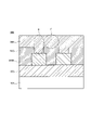
- FIG. 6 is a schematic diagram showing the configuration of a laminated structure 30C according to one embodiment of the present invention.
- the laminated structure 30C includes a substrate 100, a protective layer 400, a first alignment layer 300C-1, a second alignment layer 300C-2, and a gallium nitride film 200.
- FIG. A first alignment layer 300 C- 1 is provided on the protective layer 400 .
- a second alignment layer 300C-2 is provided on the first alignment layer 300C-1.
- the gallium nitride film 200 is provided on the second orientation layer 300C-2.
- the second alignment layer 300C-2 is patterned into a predetermined pattern. Patterning of the second alignment layer 300C-2 can be performed, for example, using photolithography. As shown in FIG. 6, the second alignment layer 300C-2 is patterned to expose a portion of the first alignment layer 300C-1. Therefore, the gallium nitride film 200 includes a region C contacting the first orientation layer 300C-1 and a region D contacting the second orientation layer 300C-2. Since the surface on which the gallium nitride film 200 is formed differs between the region C and the region D, the degree of crystal growth of the gallium nitride film 200 (for example, the ratio of c-axis orientation (degree of orientation)) differs. Therefore, in the laminated structure 30C, the gallium nitride film 200 including regions with different crystallinity can be formed by patterning the second orientation layer 300C-2.
- FIG. 7 is a schematic diagram showing the configuration of a laminated structure 30D according to one embodiment of the present invention.
- the laminated structure 30D includes a substrate 100, a protective layer 400, a first alignment layer 300D-1, a second alignment layer 300D-2, and a gallium nitride film 200.
- FIG. A first alignment layer 300 D- 1 is provided on the protective layer 400 .
- a second alignment layer 300D-2 is provided on the first alignment layer 300D-1.
- the gallium nitride film 200 is provided on the second orientation layer 300D-2.
- the first alignment layer 300D-1 is patterned into a predetermined pattern.
- the patterning of the first alignment layer 300D-1 can be performed using photolithography, for example.
- the first alignment layer 300D-1 is patterned such that a portion of the protective layer 400 is exposed.
- the exposed part of the protective layer 400 is covered by the second alignment layer 300D-2 together with the first alignment layer 300D-1. That is, the second alignment layer 300D-2 includes a region formed on the first alignment layer 300D-1 and a region formed on the protective layer 400.
- FIG. Each region has a different degree of crystal growth
- the second orientation layer 300D-2 includes regions with different c-axis orientation or surface roughness.
- the gallium nitride film 200 formed on such a second orientation layer 300D-2 also includes regions of different crystallinity corresponding to the respective regions of the second orientation layer 300D-2. Become. Therefore, in the laminated structure 30D, the gallium nitride film 200 including regions with different crystallinity can be formed by patterning the first orientation layer 300D-1.
- the laminated structure 30D When using the laminated structure 30D for a backplane, it is possible to provide a backplane in which the crystallinity of the gallium nitride film 200 is controlled. Further, by using the uneven patterns of the first alignment layer 300D-1 and the second alignment layer 300D-2 as shown in FIG. 7, it is possible to control the light from the light emitting element and improve the light extraction efficiency. can.
- FIG. 8 is a schematic diagram showing the configuration of a laminated structure 40 according to one embodiment of the present invention.
- the laminated structure 30 includes a substrate 100 , a protective layer 400 , an orientation layer 300 , a non-orientation layer 500 and a gallium nitride film 200 .
- the alignment layer 300 is provided on the protective layer 400 .
- a non-orientation layer 500 is provided on the orientation layer 300 .
- the gallium nitride film 200 is formed on the non-oriented layer 500 using sputtering.
- the configuration of the laminated structure 40 is the same as that of the laminated structure 10, the laminated structure 20, and the laminated structure 30, the explanation may be omitted.
- the non-oriented layer 500 can reduce the crystallinity of the gallium nitride film 200 . That is, the gallium nitride film 200 formed on the non-oriented layer 500 has low crystallinity.
- the non-orientation layer 500 for example, an amorphous material such as silicon oxide can be used. By making the non-formation surface of the gallium nitride film 200 amorphous, the crystal growth of the gallium nitride film 200 can be inhibited.
- the non-orientation layer 500 is patterned into a predetermined pattern. Patterning of the non-orientation layer 500 can be performed, for example, using photolithography. As shown in FIG. 8, the non-orientation layer 500 is patterned such that a portion of the orientation layer 300 is exposed. Therefore, the gallium nitride film 200 includes a region E contacting the oriented layer 300 and a region F contacting the non-oriented layer 500 . In region E, crystal growth of gallium nitride film 200 is promoted, and in region F, crystal growth of gallium nitride film 200 is inhibited. That is, the gallium nitride film 200 of the laminated structure 40 includes regions E with high crystallinity and regions F with low crystallinity. Therefore, in the laminated structure 40, by providing the non-oriented layer 500 and patterning the non-oriented layer 500, the gallium nitride film 200 including regions with different crystallinity can be formed.
- FIG. 9 is a schematic diagram showing the configuration of a laminated structure 40E according to one embodiment of the present invention.
- the laminated structure 40E includes a substrate 100, a protective layer 400, an orientation layer 300E, a non-orientation layer 500, and a gallium nitride film 200.
- FIG. The alignment layer 300E is provided on the protective layer 400.
- the non-orientation layer 500 is provided on the orientation layer 300E.
- the gallium nitride film 200 is formed on the non-oriented layer 500 using sputtering.
- the gallium nitride film 200 includes a region E in contact with the oriented layer 300 and a region F in contact with the non-oriented layer 500.
- the gallium nitride film 200 of the laminated structure 40E also includes regions E with high crystallinity and regions F with low crystallinity. Therefore, the gallium nitride film 200 including regions with different crystallinity can be formed also in the laminated structure 40E.
- FIG. 10 is a schematic diagram showing a laminated structure 40F according to one embodiment of the invention.
- a laminated structure 40F includes a substrate 100, a protective layer 400, a non-oriented layer 500F, an oriented layer 300F, and a gallium nitride film 200.
- FIG. A non-orientation layer 500F is provided on the protective layer 400 .
- the orientation layer 300F is provided on the non-orientation layer 500F.
- the gallium nitride film 200 is formed on the orientation layer 300F using sputtering.
- a non-oriented layer 500F having a predetermined pattern is covered with an oriented layer 300F. That is, the alignment layer 300F includes a region formed over the non-alignment layer 500F and a region formed over the protective layer 400. FIG. Each region has a different degree of crystal growth, and the orientation layer 300F includes regions with different c-axis orientations or different surface roughnesses. Further, the gallium nitride film 200 formed on such an orientation layer 300F also includes regions with different crystallinity corresponding to the respective regions of the orientation layer 300F. Therefore, in the laminated structure 40F, the gallium nitride film 200 including regions with different crystallinity can be formed by forming the orientation layer 300F so as to cover the patterned non-orientation layer 500F.
- the laminated structure 40F for a backplane, it is possible to provide a backplane in which the crystallinity of the gallium nitride film 200 is controlled. Moreover, by using the uneven pattern of the non-oriented layer 500F and the oriented layer 300F as shown in FIG. 10, the light from the light emitting element can be controlled and the light extraction efficiency can be improved.
- FIG. 11 is a schematic diagram showing the configuration of a light emitting device 1000 using the laminated structure 30 according to one embodiment of the present invention.
- the light emitting device 1000 includes a laminated structure 30, an n-type semiconductor layer 1040, a light emitting layer 1050, a p-type semiconductor layer 1060, an n-type electrode 1070, and a p-type electrode 1080.
- the light emitting element 1000 is a so-called LED (Light Emitting Diode), but is not limited to this.
- a silicon-doped gallium nitride film or the like can be used as the n-type semiconductor layer 1040 .
- the light-emitting layer 1050 a stacked body in which an indium gallium nitride film and a gallium nitride film are alternately stacked can be used.
- the p-type semiconductor layer 1060 a magnesium-doped gallium nitride film or the like can be used.
- a metal such as indium can be used as the n-type electrode 1070 .
- a metal such as palladium or gold can be used as the p-type electrode 1080 .
- the manufacturing method of the light emitting device 1000 is as follows.
- a silicon-doped gallium nitride film is formed on the laminated structure 30 . Further, an indium gallium nitride film and a gallium nitride film are alternately formed on a silicon-doped gallium nitride film to form a laminate. Further, a magnesium-doped gallium nitride film is formed on the laminate.
- the magnesium-doped gallium film, the laminate, and the silicon-doped gallium nitride film are etched using photolithography to form the p-type semiconductor layer 1060, the light-emitting layer 1050, and the n-type semiconductor layer 1040. .
- etching is performed so as to expose a part of the surface of the silicon-doped gallium nitride film.
- An n-type electrode 1070 and a p-type electrode 1080 are formed on the n-type semiconductor layer 1040 and the p-type semiconductor layer 1060, respectively.
- a silicon-doped gallium nitride film, an indium gallium nitride film, and a magnesium-doped gallium nitride film can be deposited using a sputtering ring.
- a silicon-doped gallium nitride film, an indium gallium nitride film, and a magnesium-doped gallium nitride film can be continuously formed by connecting a plurality of vacuum chambers via a substrate transfer section without breaking the vacuum. can do.
- the light-emitting element 1000 can be manufactured using the laminated structure 30 . Since the laminated structure 30 includes the substrate 100 that can have a large area, and the light-emitting element 1000 is manufactured using a large-area substrate, the manufacturing cost of the light-emitting element 1000 can be suppressed.
- FIG. 12 is a schematic diagram showing the configuration of a semiconductor device 2000 using the laminated structure 30 according to one embodiment of the present invention.
- a semiconductor device 2000 includes a laminated structure 30, a first aluminum gallium nitride layer 2050, a second aluminum gallium nitride layer 2060, a third aluminum gallium nitride layer 2070, a source electrode 2080, a drain electrode and a 2090 , a gate electrode 2100 , a first insulating layer 2110 , a second insulating layer 2120 and a shield electrode 2130 .
- the semiconductor element 2000 is a so-called HEMT (High Electron Mobility Transistor), but is not limited to this.
- An aluminum gallium nitride film can be used as the first aluminum gallium nitride layer 2050 .
- As the second aluminum gallium nitride layer 2060 for example, a silicon-doped aluminum gallium nitride film can be used.
- An aluminum gallium nitride film can be used as the third aluminum gallium nitride layer 2070 .
- a metal such as titanium or aluminum can be used for the source electrode 2080 and the drain electrode 2090, for example.
- a metal such as nickel or gold can be used as the gate electrode 2100, for example.
- As the first insulating layer 2110 for example, a silicon nitride film can be used.
- As the second insulating layer 2120 for example, a silicon oxide film can be used.
- As the shield electrode 2130 for example, laminated metal such as aluminum/titanium (Al/Ti) can be used.
- the manufacturing method of the semiconductor device 2000 is as follows.
- a first aluminum gallium nitride layer 2050 is formed on the laminated structure 30 .
- a silicon-doped aluminum gallium nitride film and an aluminum gallium nitride film are formed on the first aluminum gallium nitride layer 2050 .
- the aluminum gallium nitride film and the silicon-doped aluminum gallium nitride film are then etched using photolithography to form a third aluminum gallium nitride layer 2070 and a second aluminum gallium nitride layer 2060 . At this time, etching is performed so as to partially expose the surface of the silicon-doped aluminum gallium nitride film.
- a source electrode 2080 and a drain electrode 2090 are formed over the second aluminum gallium nitride layer 2060 . Also, a gate electrode 2100 is formed on the third aluminum gallium nitride layer 2070 . A silicon nitride film and a silicon oxide film are sequentially formed to cover the source electrode 2080 , the drain electrode 2090 , and the gate electrode 2100 to form a first insulating layer 2110 and a second insulating layer 2120 . A shield electrode 2130 is formed on the second insulating layer 2120 .
- Aluminum gallium nitride films and silicon-doped aluminum gallium nitride films can be deposited using a sputtering ring.
- the semiconductor element 2000 can be manufactured using the laminated structure 30 . Since the laminated structure 30 includes the substrate 100 that can be increased in area, a large-area backplane in which the semiconductor elements 2000 are integrated can be manufactured.
Abstract
This laminated structure comprises a substrate and a gallium nitride film disposed on the substrate. The arithmetic mean roughness (Ra) of the substrate surface is less than 0.33 nm. Alternatively, the laminated structure comprises: a substrate; an alignment layer which is disposed on the substrate and which has a c-axis orientation or a (111) orientation of a face-centered cubic structure; and a gallium nitride film disposed on the alignment layer. The arithmetic mean roughness (Ra) of the substrate surface is less than 0.33 nm. Alternatively, the laminated structure comprises: a substrate; a protective layer disposed on the substrate; an alignment layer which is disposed on the protective layer and which has a c-axis orientation or a (111) orientation of a face-centered cubic structure; and a gallium nitride film disposed on the alignment layer. The arithmetic mean roughness (Ra) of the substrate surface is less than 0.33.
Description
本発明の一実施形態は、基板上に形成された窒化ガリウム膜を含む積層構造体に関する。
One embodiment of the present invention relates to a laminated structure including a gallium nitride film formed on a substrate.
窒化ガリウム(GaN)は、バンドギャップの大きい直接遷移半導体という特徴を有する。この窒化ガリウムの特徴を利用し、窒化ガリウムを用いた発光ダイオード(LED)が既に実用化されている。また、窒化ガリウムは、電子飽和移動度および耐圧が高い特徴も有する。近年では、この窒化ガリウムの特徴を利用し、高周波パワーデバイス用途のトランジスタの開発が進められている。発光ダイオードまたはトランジスタの窒化ガリウム膜は、一般的に、サファイア基板上に、MOCVD(Metal Organic Chemical Vapor Deposition)またはHVPE(Hydride Vapor Phase Epitaxy)を用いて800℃~1000℃という高温で成膜されている。
Gallium nitride (GaN) is characterized as a direct bandgap semiconductor with a large bandgap. Taking advantage of this feature of gallium nitride, light-emitting diodes (LEDs) using gallium nitride have already been put to practical use. In addition, gallium nitride also has the characteristics of high electron saturation mobility and high breakdown voltage. In recent years, utilizing the characteristics of gallium nitride, the development of transistors for high-frequency power devices is underway. Gallium nitride films for light-emitting diodes or transistors are generally formed on sapphire substrates at high temperatures of 800° C. to 1000° C. using MOCVD (Metal Organic Chemical Vapor Deposition) or HVPE (Hydride Vapor Phase Epitaxy). there is
ところで、近年、次世代表示装置として、回路基板の画素内に微小な発光ダイオードチップを実装した、いわゆるマイクロLED表示装置またはミニLED表示装置の開発が進められている。マイクロLED表示装置またはミニLED表示装置は、高効率、高輝度、および高信頼性を有する。このようなマイクロLED表示装置またはミニLED表示装置は、酸化物半導体または低温ポリシリコンなどを用いたトランジスタが形成されたバックプレーンに、LEDチップが転写されることによって製造される(例えば、特許文献1参照)。また、同一基板上に窒化ガリウムを含むトランジスタと発光ダイオードとを形成する方法も検討されている(例えば、特許文献2参照)。
By the way, in recent years, as next-generation display devices, so-called micro-LED display devices or mini-LED display devices, in which minute light-emitting diode chips are mounted in the pixels of a circuit board, have been developed. Micro LED display or mini LED display has high efficiency, high brightness and high reliability. Such a micro-LED display device or mini-LED display device is manufactured by transferring an LED chip to a backplane on which a transistor using an oxide semiconductor or low-temperature polysilicon is formed (see, for example, Patent Documents 1). Further, a method of forming a transistor containing gallium nitride and a light-emitting diode over the same substrate has also been studied (see Patent Document 2, for example).
上述したように、一般的には、窒化ガリウム膜はサファイア基板上に高温で成膜される。非晶質ガラス基板のような大面積基板は耐熱性が低く、低温で成膜した窒化ガリウム膜は結晶性が低いという問題があった。また、大面積のバックプレーンを提供することが難しいという問題もあった。
As described above, gallium nitride films are generally formed on sapphire substrates at high temperatures. A large-area substrate such as an amorphous glass substrate has low heat resistance, and a gallium nitride film formed at a low temperature has a problem of low crystallinity. Another problem is that it is difficult to provide a large-area backplane.
本発明の一実施形態は、上記問題に鑑み、大面積化が可能な基板に結晶性の高い窒化ガリウム膜が形成された積層構造体を提供することを目的の一つとする。
In view of the above problem, one object of an embodiment of the present invention is to provide a laminated structure in which a highly crystalline gallium nitride film is formed on a substrate that can be increased in area.
本発明の一実施形態に係る積層構造体は、基板と、基板上の窒化ガリウム膜と、を含み、基板の表面の算術平均粗さ(Ra)は、0.33nmよりも小さい。
A laminated structure according to one embodiment of the present invention includes a substrate and a gallium nitride film on the substrate, and the surface arithmetic mean roughness (Ra) of the substrate is less than 0.33 nm.
本発明の一実施形態に係る積層構造体は、基板と、基板上のc軸配向または面心立方構造の(111)配向を有する配向層と、配向層上の窒化ガリウム膜と、を含み、基板の表面の算術平均粗さ(Ra)は、0.33nmよりも小さい。
A laminated structure according to one embodiment of the present invention includes a substrate, an orientation layer having c-axis orientation or face-centered cubic (111) orientation on the substrate, and a gallium nitride film on the orientation layer, The surface arithmetic mean roughness (Ra) of the substrate is less than 0.33 nm.
本発明の一実施形態に係る積層構造体は、基板と、基板上の保護層と、保護層上のc軸配向または面心立方構造の(111)配向を有する配向層と、配向層上の窒化ガリウム膜と、を含み、基板の表面の算術平均粗さ(Ra)は、0.33nmよりも小さい。
A laminated structure according to one embodiment of the present invention includes a substrate, a protective layer on the substrate, an orientation layer having c-axis orientation or face-centered cubic (111) orientation on the protective layer, and and a gallium nitride film, and the surface arithmetic mean roughness (Ra) of the substrate is less than 0.33 nm.
以下、本発明に係る各実施形態について、図面を参照しつつ説明する。なお、各実施形態はあくまで一例にすぎず、当業者が、発明の主旨を保ちつつ適宜変更することによって容易に想到し得るものについても、当然に本発明の範囲に含まれる。また、図面は、説明をより明確にするため、実際の態様に比べ、各部の幅、厚さ、または形状などが模式的に表される場合がある。しかし、図示された形状などはあくまで一例であって、本発明の解釈を限定するものではない。
Hereinafter, each embodiment according to the present invention will be described with reference to the drawings. It should be noted that each embodiment is merely an example, and those that can be easily conceived by those skilled in the art by making appropriate modifications while maintaining the gist of the invention are naturally included in the scope of the present invention. Also, in order to make the description clearer, the drawings may schematically represent the width, thickness, shape, etc. of each part compared to the actual mode. However, the illustrated shapes and the like are merely examples, and do not limit the interpretation of the present invention.
本明細書において「αはA、BまたはCを含む」、「αはA、BおよびCのいずれかを含む」、「αはA、BおよびCからなる群から選択される一つを含む」、といった表現は、特に明示が無い限り、αがA~Cの複数の組み合わせを含む場合を排除しない。さらに、これらの表現は、αが他の要素を含む場合も排除しない。
In the present specification, "α includes A, B or C", "α includes any one of A, B and C", "α includes one selected from the group consisting of A, B and C ”, does not exclude the case where α includes a plurality of combinations of A to C, unless otherwise specified. Furthermore, these expressions do not exclude the case where α contains other elements.
本明細書において、説明の便宜上、「上」または「上方」もしくは「下」または「下方」という語句を用いて説明するが、原則として、構造物が形成される基板を基準とし、基板から構造物に向かう方向を「上」または「上方」とする。逆に、構造物から基板に向かう方向を「下」または「下方」とする。したがって、基板上の構造物という表現において、基板と向き合う方向の構造物の面が構造物の下面となり、その反対側の面が構造物の上面となる。また、基板上の構造物という表現においては、基板と構造物との上下関係を説明しているに過ぎず、基板と構造物との間に他の部材が配置されていてもよい。さらに、「上」または「上方」もしくは「下」または「下方」の語句は、複数の層が積層された構造における積層順を意味するものであり、平面視において重畳する位置関係になくてもよい。
In this specification, for convenience of explanation, the terms “upper”, “upper”, “lower”, and “lower” are used, but in principle, the substrate on which the structure is formed is used as a reference, and the structure is formed from the substrate. Let the direction toward an object be "up" or "upper". Conversely, the direction from the structure toward the substrate is defined as "down" or "lower". Therefore, in the expression of the structure on the substrate, the surface of the structure facing the substrate is the lower surface of the structure, and the opposite surface is the upper surface of the structure. In addition, the expression "structure on the substrate" merely describes the vertical relationship between the substrate and the structure, and other members may be arranged between the substrate and the structure. Furthermore, the terms "upper" or "upper" or "lower" or "lower" mean the order of stacking in a structure in which a plurality of layers are stacked, even if they are not in an overlapping positional relationship in plan view. good.
本明細書において、各構成に付記される「第1」、「第2」、または「第3」などの文字は、各構成を区別するために用いられる便宜的な標識であり、特段の説明がない限り、それ以上の意味を有さない。
In this specification, letters such as “first”, “second”, or “third” attached to each configuration are convenient marks used to distinguish each configuration, and has no further meaning unless
本明細書および図面において、同一または類似する複数の構成を総じて表記する際には同一の符号を用い、これらの複数の構成のそれぞれを区別して表記する際には、小文字または大文字のアルファベットを添えて表記する場合がある。また、1つの構成のうちの複数の部分を区別して表記する際には、ハイフンと自然数を用いる場合がある。
In the present specification and drawings, the same reference numerals are used to collectively denote a plurality of configurations that are the same or similar, and lower-case or upper-case letters are added to distinguish between the plurality of configurations. may be written as In addition, hyphens and natural numbers may be used when distinguishing and notating a plurality of parts in one configuration.
以下の各実施形態は、技術的な矛盾を生じない限り、互いに組み合わせることができる。
The following embodiments can be combined with each other as long as there is no technical contradiction.
<第1実施形態>
図1は、本発明の一実施形態に係る積層構造体の構成を示す概略図である。積層構造体10は、基板100および窒化ガリウム膜200を含む。窒化ガリウム膜200は、基板100上にスパッタリングを用いて形成される。 <First Embodiment>
FIG. 1 is a schematic diagram showing the configuration of a laminated structure according to one embodiment of the present invention. A laminatedstructure 10 includes a substrate 100 and a gallium nitride film 200 . A gallium nitride film 200 is formed on the substrate 100 using sputtering.
図1は、本発明の一実施形態に係る積層構造体の構成を示す概略図である。積層構造体10は、基板100および窒化ガリウム膜200を含む。窒化ガリウム膜200は、基板100上にスパッタリングを用いて形成される。 <First Embodiment>
FIG. 1 is a schematic diagram showing the configuration of a laminated structure according to one embodiment of the present invention. A laminated
基板100は、窒化ガリウム膜200の支持基板である。積層構造体10の窒化ガリウム膜200はスパッタリングによって成膜されるため、基板100は、例えば、600℃程度の耐熱性を有すればよい。そのため、基板100として、例えば、非晶質ガラス基板を用いることができる。また、基板100として、ポリイミド基板、アクリル基板、シロキサン基板、またはフッ素樹脂基板などの樹脂基板も用いることができる。なお、非晶質ガラス基板または樹脂基板は、大面積化が可能な基板である。また、基板100として、多結晶基板を用いることもできる。多結晶基板は、窒化ガリウム膜の通常の成膜で用いられるサファイア基板よりも大きいため、ガラス基板または樹脂基板と同様に、バックプレーンとして用いることが可能である。
The substrate 100 is a support substrate for the gallium nitride film 200 . Since the gallium nitride film 200 of the laminated structure 10 is formed by sputtering, the substrate 100 may have heat resistance of about 600° C., for example. Therefore, for example, an amorphous glass substrate can be used as the substrate 100 . Alternatively, as the substrate 100, a resin substrate such as a polyimide substrate, an acrylic substrate, a siloxane substrate, or a fluororesin substrate can be used. Note that an amorphous glass substrate or a resin substrate is a substrate that can have a large area. A polycrystalline substrate can also be used as the substrate 100 . Since the polycrystalline substrate is larger than the sapphire substrate used in normal film formation of gallium nitride films, it can be used as a backplane in the same manner as a glass substrate or a resin substrate.
非晶質ガラスなどの基板100上の窒化ガリウム膜200の結晶成長は、基板100の表面状態の影響を受ける。特に、基板100の表面の凹凸は、ランダムな結晶核を発生させる要因となる。その結果、ランダムな方向への窒化ガリウムの結晶成長が起こり、また、隣接する結晶が互いに干渉し、結晶成長が阻害される。したがって、基板100は、凹凸が少なく、平滑な表面を有することが好ましい。例えば、基板100の表面の算術平均粗さ(Ra)は、0.33nmよりも小さいことが好ましい。また、基板100の表面の二乗平均平方根粗さ(Rq)は、0.39nmよりも小さいことが好ましい。基板100の表面粗さが上記条件である場合、基板100が非晶質でガラス基板であっても、窒化ガリウム膜200の結晶性を向上させることができる。換言すると、基板100上に、c軸配向((0001)面を表面とした配向)を有する窒化ガリウム膜200を形成することができる。
The crystal growth of the gallium nitride film 200 on the substrate 100 such as amorphous glass is affected by the surface state of the substrate 100 . In particular, unevenness on the surface of the substrate 100 is a factor in generating random crystal nuclei. As a result, crystal growth of gallium nitride occurs in random directions, and adjacent crystals interfere with each other, inhibiting crystal growth. Therefore, the substrate 100 preferably has a smooth surface with few irregularities. For example, the arithmetic mean roughness (Ra) of the surface of substrate 100 is preferably less than 0.33 nm. Also, the root mean square roughness (Rq) of the surface of the substrate 100 is preferably less than 0.39 nm. When the surface roughness of the substrate 100 satisfies the above conditions, the crystallinity of the gallium nitride film 200 can be improved even if the substrate 100 is amorphous and is a glass substrate. In other words, the gallium nitride film 200 having c-axis orientation (orientation with the (0001) plane as the surface) can be formed on the substrate 100 .
ここで、スパッタリングを用いた窒化ガリウム膜200の成膜について説明する。
Here, deposition of the gallium nitride film 200 using sputtering will be described.
真空チャンバ内に、窒化ガリウムターゲットと対向して基板100を配置する。窒化ガリウムターゲットにおける窒化ガリウムの組成比は、窒素に対するガリウムが0.7以上2以下であることが好ましい。また、真空チャンバには、スパッタリングガス(アルゴンまたはクリプトンなど)とは別に、窒素を供給することができる。その場合、窒化ガリウムターゲットの窒化ガリウムの組成比は、窒素よりもガリウムが多いことが好ましい。例えば、窒素は、窒素ラジカル供給源を用いて供給することができる。スパッタリング電源は、DC電源、RF電源、またはパルスDC電源のいずれであってもよい。
A substrate 100 is placed in a vacuum chamber facing a gallium nitride target. The composition ratio of gallium nitride in the gallium nitride target is preferably 0.7 or more and 2 or less of gallium to nitrogen. Nitrogen can also be supplied to the vacuum chamber separately from the sputtering gas (such as argon or krypton). In that case, it is preferable that the composition ratio of gallium nitride in the gallium nitride target is more gallium than nitrogen. For example, nitrogen can be supplied using a nitrogen radical source. The sputtering power supply can be either a DC power supply, an RF power supply, or a pulsed DC power supply.
真空チャンバ内の基板100は、加熱されてもよい。例えば、基板100は、400℃以上600℃未満で加熱することができる。この基板温度であれば、耐熱性の低い非晶質ガラス基板に対しても適用することができる。また、この基板温度は、MOCVDまたはHVPEでの成膜温度よりも低い。
The substrate 100 inside the vacuum chamber may be heated. For example, the substrate 100 can be heated at 400.degree. C. or more and less than 600.degree. This substrate temperature can be applied to an amorphous glass substrate having low heat resistance. Also, this substrate temperature is lower than the deposition temperature in MOCVD or HVPE.
真空チャンバ内を十分排気した後、スパッタリングガスを供給する。また、所定の圧力で基板100と窒化ガリウムターゲットとの間に電圧を印加してプラズマを生成し、窒化ガリウム膜200を成膜する。表面粗さが制御された基板100上に窒化ガリウム膜200が形成されているため、窒化ガリウム膜200はc軸配向を有する。
After the vacuum chamber is sufficiently exhausted, the sputtering gas is supplied. Also, a voltage is applied between the substrate 100 and the gallium nitride target at a predetermined pressure to generate plasma, and the gallium nitride film 200 is formed. Since the gallium nitride film 200 is formed on the substrate 100 whose surface roughness is controlled, the gallium nitride film 200 has a c-axis orientation.
本実施形態に係る積層構造体10は、結晶性が高く、c軸配向を有する窒化ガリウム膜200を含む。また、積層構造体10は、大面積化が可能な基板100を含む。そのため、積層構造体10を利用することにより、窒化ガリウムを含むLEDの生産性を高め、または窒化ガリウムを含むトランジスタが形成されたバックプレーンを作製することができる。
The laminated structure 10 according to the present embodiment includes a gallium nitride film 200 with high crystallinity and c-axis orientation. Moreover, the laminated structure 10 includes a substrate 100 that can have a large area. Therefore, by using the laminated structure 10, it is possible to increase the productivity of LEDs containing gallium nitride, or to manufacture backplanes on which transistors containing gallium nitride are formed.
<第2実施形態>
図2は、本発明の一実施形態に係る積層構造体20の構成を示す概略図である。積層構造体20は、基板100、配向層300、および窒化ガリウム膜200を含む。配向層300は、基板100上に設けられている。また、窒化ガリウム膜200は、配向層300上にスパッタリングを用いて形成される。なお、以下では、積層構造体20の構成が、積層構造体10の構成と同様であるときは、その説明を省略することがある。 <Second embodiment>
FIG. 2 is a schematic diagram showing the configuration of alaminated structure 20 according to one embodiment of the present invention. The laminated structure 20 includes a substrate 100 , an alignment layer 300 and a gallium nitride film 200 . An alignment layer 300 is provided on the substrate 100 . Also, the gallium nitride film 200 is formed on the alignment layer 300 using sputtering. In the following, when the configuration of the laminated structure 20 is the same as the configuration of the laminated structure 10, the explanation may be omitted.
図2は、本発明の一実施形態に係る積層構造体20の構成を示す概略図である。積層構造体20は、基板100、配向層300、および窒化ガリウム膜200を含む。配向層300は、基板100上に設けられている。また、窒化ガリウム膜200は、配向層300上にスパッタリングを用いて形成される。なお、以下では、積層構造体20の構成が、積層構造体10の構成と同様であるときは、その説明を省略することがある。 <Second embodiment>
FIG. 2 is a schematic diagram showing the configuration of a
配向層300は、窒化ガリウム膜200の結晶性を向上させることができる。すなわち、配向層300は、窒化ガリウム膜200のc軸配向性をさらに向上させることができる。平滑な基板100上においても、六方最密構造を有する窒化ガリウム膜200は、表面エネルギーを最小化するようにc軸配向するが、基板100上に配向層300を設けることで、窒化ガリウム膜200のc軸配向性を制御することができる。具体的には、配向層300の材料の種類によって窒化ガリウム膜200のc軸配向性を制御する。配向層300は、六方最密構造、面心立方構造、またはそれらに準ずる構造を有する材料を用いることができる。ここで、六方最密構造または面心立方構造に準ずる構造とは、a軸およびb軸に対してc軸が90°とならない結晶構造を含むものである。六方最密構造およびそれに準ずる構造を有する材料では、基板100に対して(0001)方向、すなわち、c軸方向に配向することができる(以下、六方最密構造の(0001)配向またはc軸配向という。)。また、面心立方構造およびそれに準ずる構造を有する材料では、基板100に対して(111)方向に配向することができる(以下、これを面心立方構造の(111)配向という。)。配向層300がc軸配向または面心立方構造の(111)配向を有することにより、窒化ガリウム膜200もc軸配向しやすくなる。配向層300として、例えば、チタン(Ti)、窒化チタン(TiNx)、酸化チタン(TiOx)、グラフェン、酸化亜鉛(ZnO)、二ホウ化マグネシウム(MgB2)、アルミニウム(Al)、窒化アルミニウム(AlN)、酸化アルミニウム(Al2O3)、銀(Ag)、カルシウム(Ca)、ニッケル(Ni)、銅(Cu)、ストロンチウム(Sr)、ロジウム(Rh)、パラジウム(Pd)、セリウム(Ce)、イッテルビウム(Yb)、イリジウム(Ir)、白金(Pt)、金(Au)、鉛(Pb)、アクチニウム(Ac)、トリウム(Th)、ニオブ酸リチウム(LiNbO)、BiLaTiO、SrFeO、SrFeO、BiFeO、BaFeO、ZnFeO、PMnN-PZT、または生体アパタイト(BAp)などを用いることができる。特に、配向層300として、チタン、グラフェン、酸化亜鉛、窒化アルミニウム、または酸化アルミニウムを用いることが好ましい。また、配向層300の膜厚は、例えば、50nm以上である。なお、配向層300の成膜は、スパッタリングに限られない。配向層300は、CVDなど任意の方法(装置)を用いて成膜することができる。
The orientation layer 300 can improve the crystallinity of the gallium nitride film 200 . That is, the orientation layer 300 can further improve the c-axis orientation of the gallium nitride film 200 . The gallium nitride film 200 having a hexagonal close-packed structure is oriented along the c-axis so as to minimize the surface energy even on the smooth substrate 100 . can control the c-axis orientation of Specifically, the c-axis orientation of the gallium nitride film 200 is controlled by the type of material of the orientation layer 300 . The alignment layer 300 can use a material having a hexagonal close-packed structure, a face-centered cubic structure, or a structure conforming thereto. Here, the structure conforming to the hexagonal close-packed structure or the face-centered cubic structure includes a crystal structure in which the c-axis is not 90° with respect to the a-axis and the b-axis. A material having a hexagonal close-packed structure or a structure equivalent thereto can be oriented in the (0001) direction, that is, in the c-axis direction with respect to the substrate 100 (hereinafter referred to as the (0001) orientation of the hexagonal close-packed structure or the c-axis orientation. called.). In addition, materials having a face-centered cubic structure or a structure similar thereto can be oriented in the (111) direction with respect to the substrate 100 (hereinafter referred to as (111) orientation of the face-centered cubic structure). When the orientation layer 300 has the c-axis orientation or the (111) orientation of the face-centered cubic structure, the gallium nitride film 200 is also easily c-axis oriented. Examples of the orientation layer 300 include titanium (Ti), titanium nitride (TiN x ), titanium oxide (TiO x ), graphene, zinc oxide (ZnO), magnesium diboride (MgB 2 ), aluminum (Al), and aluminum nitride. (AlN), aluminum oxide ( Al2O3 ) , silver (Ag), calcium (Ca), nickel (Ni), copper (Cu), strontium (Sr), rhodium (Rh), palladium (Pd), cerium ( Ce), ytterbium (Yb), iridium (Ir), platinum (Pt), gold (Au), lead (Pb), actinium (Ac), thorium (Th), lithium niobate (LiNbO), BiLaTiO, SrFeO, SrFeO , BiFeO, BaFeO, ZnFeO, PMnN-PZT, or biogenic apatite (BAp) can be used. In particular, it is preferable to use titanium, graphene, zinc oxide, aluminum nitride, or aluminum oxide as the alignment layer 300 . Also, the film thickness of the alignment layer 300 is, for example, 50 nm or more. Note that the deposition of the alignment layer 300 is not limited to sputtering. The alignment layer 300 can be deposited using any method (apparatus) such as CVD.
窒化ガリウム膜200の結晶性は、上述したように、非成膜面の表面状態の影響を受ける。すなわち、積層構造体20では、窒化ガリウム膜200は、配向層300の表面状態の影響を受ける。したがって、配向層300は、凹凸が少なく、平滑な表面を有することが好ましい。例えば、配向層300の表面の算術平均粗さ(Ra)は、2.3nmよりも小さいことが好ましい。また、配向層300の表面の二乗平均平方根粗さ(Rq)は、2.9nmよりも小さいことが好ましい。配向層300の表面粗さが上記条件である場合、c軸配向を有する窒化ガリウム膜200を形成することができる。
The crystallinity of the gallium nitride film 200 is affected by the surface state of the non-film-forming surface, as described above. That is, in the laminated structure 20 , the gallium nitride film 200 is affected by the surface state of the orientation layer 300 . Therefore, the alignment layer 300 preferably has a smooth surface with few irregularities. For example, the surface arithmetic mean roughness (Ra) of the alignment layer 300 is preferably less than 2.3 nm. Also, the root-mean-square roughness (Rq) of the surface of the alignment layer 300 is preferably less than 2.9 nm. When the surface roughness of the orientation layer 300 is under the above conditions, the gallium nitride film 200 having c-axis orientation can be formed.
なお、配向層300は、基板100上に形成されるため、配向層300の結晶性は、少なからず基板100の表面粗さの影響を受ける。そのため、積層構造体20においても、基板100は、凹凸が少なく、平滑な表面を有することが好ましい。例えば、基板100の表面の算術平均粗さ(Ra)は、0.33nmよりも小さいことが好ましい。また、基板100の表面の二乗平均平方根粗さ(Rq)は、0.39nmよりも小さいことが好ましい。
Since the orientation layer 300 is formed on the substrate 100, the crystallinity of the orientation layer 300 is affected by the surface roughness of the substrate 100 to some extent. Therefore, also in the laminated structure 20, the substrate 100 preferably has a smooth surface with little unevenness. For example, the arithmetic mean roughness (Ra) of the surface of substrate 100 is preferably less than 0.33 nm. Also, the root mean square roughness (Rq) of the surface of the substrate 100 is preferably less than 0.39 nm.
本実施形態に係る積層構造体20は、結晶性が高く、c軸配向を有する窒化ガリウム膜200を含む。また、積層構造体20は、大面積化が可能な基板100を含む。そのため、積層構造体20を利用することにより、窒化ガリウムを含むLEDの生産性を高め、または窒化ガリウムを含むトランジスタが形成されたバックプレーンを作製することができる。
The laminated structure 20 according to the present embodiment includes a gallium nitride film 200 with high crystallinity and c-axis orientation. In addition, the laminated structure 20 includes a substrate 100 that can have a large area. Therefore, by using the laminated structure 20, it is possible to increase the productivity of LEDs containing gallium nitride or to fabricate backplanes on which transistors containing gallium nitride are formed.
<第3実施形態>
図3は、本発明の一実施形態に係る積層構造体30の構成を示す概略図である。積層構造体30は、基板100、保護層400、配向層300、窒化ガリウム膜200を含む。保護層400は、基板100上に設けられている。配向層300は、保護層400上に設けられている。また、窒化ガリウム膜200は、配向層300上にスパッタリングを用いて形成される。なお、以下では、積層構造体30の構成が、積層構造体10または積層構造体20と同様の構成であるときは、その説明を省略することがある。 <Third Embodiment>
FIG. 3 is a schematic diagram showing the configuration of alaminated structure 30 according to one embodiment of the present invention. The laminated structure 30 includes a substrate 100 , a protective layer 400 , an alignment layer 300 and a gallium nitride film 200 . A protective layer 400 is provided on the substrate 100 . The alignment layer 300 is provided on the protective layer 400 . Also, the gallium nitride film 200 is formed on the alignment layer 300 using sputtering. In addition, below, when the structure of the laminated structure 30 is the structure similar to the laminated structure 10 or the laminated structure 20, the description may be abbreviate|omitted.
図3は、本発明の一実施形態に係る積層構造体30の構成を示す概略図である。積層構造体30は、基板100、保護層400、配向層300、窒化ガリウム膜200を含む。保護層400は、基板100上に設けられている。配向層300は、保護層400上に設けられている。また、窒化ガリウム膜200は、配向層300上にスパッタリングを用いて形成される。なお、以下では、積層構造体30の構成が、積層構造体10または積層構造体20と同様の構成であるときは、その説明を省略することがある。 <Third Embodiment>
FIG. 3 is a schematic diagram showing the configuration of a
保護層400は、基板100からの不純物の拡散を防止することができる。そのため、保護層400上に形成された配向層300は、不純物が少ないため、結晶性が向上する。保護層400として、例えば、酸化シリコン(SiOx)または窒化シリコン(SiNx)などを用いることができる。なお、保護層400は、単膜であってもよく、積層膜であってもよい。例えば、基板100が非晶質ガラス基板であれば、窒化シリコンと酸化シリコンとの積層膜(SiOx/SiNx)を用いることができる。また、基板100が樹脂基板であれば、窒化シリコンを酸化シリコンで挟んだ積層膜(SiOx/SiNx/SiOx)を用いることができる。
The protective layer 400 can prevent impurities from diffusing from the substrate 100 . Therefore, since the orientation layer 300 formed on the protective layer 400 has few impurities, the crystallinity is improved. Silicon oxide (SiO x ) or silicon nitride (SiN x ), for example, can be used as the protective layer 400 . In addition, the protective layer 400 may be a single film or a laminated film. For example, if the substrate 100 is an amorphous glass substrate, a laminated film (SiO x /SiN x ) of silicon nitride and silicon oxide can be used. Further, if the substrate 100 is a resin substrate, a laminated film (SiO x /SiN x /SiO x ) in which silicon nitride is sandwiched between silicon oxides can be used.
積層構造体30では、配向層300は保護層400上に成膜されるため、配向層300の結晶性は、保護層400の表面粗さの影響を受ける。そのため、積層構造体30においては、保護層400が、凹凸が少なく、平滑な表面を有することが好ましい。例えば、保護層400の表面の算術平均粗さ(Ra)は、0.51nmよりも小さいことが好ましい。また、保護層400の表面の二乗平均平方根粗さ(Rq)は、0.60nmよりも小さいことが好ましい。
In the laminated structure 30 , the orientation layer 300 is formed on the protective layer 400 , so the crystallinity of the orientation layer 300 is affected by the surface roughness of the protective layer 400 . Therefore, in the laminated structure 30, the protective layer 400 preferably has a smooth surface with little unevenness. For example, the surface arithmetic mean roughness (Ra) of the protective layer 400 is preferably less than 0.51 nm. Also, the root-mean-square roughness (Rq) of the surface of the protective layer 400 is preferably less than 0.60 nm.
本実施形態に係る積層構造体30は、結晶性が高く、c軸配向を有する窒化ガリウム膜200を含む。また、積層構造体30は、大面積化が可能な基板100を含む。そのため、積層構造体20を利用することにより、窒化ガリウムを含むLEDの生産性を高め、または窒化ガリウムを含むトランジスタが形成されたバックプレーンを作製することができる。
The laminated structure 30 according to the present embodiment includes a gallium nitride film 200 with high crystallinity and c-axis orientation. Moreover, the laminated structure 30 includes a substrate 100 that can be increased in area. Therefore, by using the laminated structure 20, it is possible to increase the productivity of LEDs containing gallium nitride or to fabricate backplanes on which transistors containing gallium nitride are formed.
以下では、本実施形態に係る積層構造体30のいくつかの変形例について説明する。
Several modifications of the laminated structure 30 according to the present embodiment will be described below.
<変形例1>
図4は、本発明の一実施形態に係る積層構造体30Aの構成を示す概略図である。積層構造体30Aは、基板100、保護層400、第1の配向層300A-1、第2の配向層300A-2、および窒化ガリウム膜200を含む。第1の配向層300A-1は、保護層400上に設けられている。第2の配向層300A-2は、第1の配向層300A-1上に設けられている。また、窒化ガリウム膜200は、第2の配向層300A-2上に設けられている。すなわち、第2の配向層300A-2は、窒化ガリウム膜200と接する。 <Modification 1>
FIG. 4 is a schematic diagram showing the configuration of alaminated structure 30A according to one embodiment of the present invention. The laminated structure 30A includes a substrate 100, a protective layer 400, a first alignment layer 300A-1, a second alignment layer 300A-2, and a gallium nitride film 200. FIG. A first alignment layer 300 A- 1 is provided on the protective layer 400 . A second alignment layer 300A-2 is provided on the first alignment layer 300A-1. Also, the gallium nitride film 200 is provided on the second orientation layer 300A-2. That is, the second alignment layer 300A-2 is in contact with the gallium nitride film 200. FIG.
図4は、本発明の一実施形態に係る積層構造体30Aの構成を示す概略図である。積層構造体30Aは、基板100、保護層400、第1の配向層300A-1、第2の配向層300A-2、および窒化ガリウム膜200を含む。第1の配向層300A-1は、保護層400上に設けられている。第2の配向層300A-2は、第1の配向層300A-1上に設けられている。また、窒化ガリウム膜200は、第2の配向層300A-2上に設けられている。すなわち、第2の配向層300A-2は、窒化ガリウム膜200と接する。 <
FIG. 4 is a schematic diagram showing the configuration of a
第1の配向層300A-1と第2の配向層300A-2とは、配向層の種類が異なる。例えば、第1の配向層300A-1および第2の配向層300A-2は、それぞれ、絶縁体および導体である。また、第1の配向層300A-1および第2の配向層300A-2が、それぞれ、導体および絶縁体であってもよい。第1の配向層300A-1および第2の配向層300A-2の各々として、上述した配向層300の材料を組み合わせて用いることができる。第1の配向層300A-1および第2の配向層300A-2の材料の組み合わせは、積層構造体30Aが利用されるデバイスを考慮して適宜選択すればよい。なお、窒化ガリウム膜200が接する第2の配向層300A-2は、第1の配向層300A-1から窒化ガリウム膜200への不純物の拡散を防止することができる材料であることが好ましい。第1の配向層300A-1および第2の配向層300A-2の材料の組み合わせは、例えば、窒化アルミニウムおよびチタン、窒化チタンおよびチタン、または酸化チタンおよびチタンなどであるが、これに限られない。
The first alignment layer 300A-1 and the second alignment layer 300A-2 are different in type of alignment layer. For example, the first alignment layer 300A-1 and the second alignment layer 300A-2 are insulators and conductors, respectively. Also, the first alignment layer 300A-1 and the second alignment layer 300A-2 may be conductors and insulators, respectively. As each of the first alignment layer 300A-1 and the second alignment layer 300A-2, the materials of the alignment layer 300 described above can be used in combination. A combination of materials for the first alignment layer 300A-1 and the second alignment layer 300A-2 may be appropriately selected in consideration of the device in which the laminated structure 30A is used. The second orientation layer 300A-2 with which the gallium nitride film 200 is in contact is preferably made of a material capable of preventing diffusion of impurities from the first orientation layer 300A-1 to the gallium nitride film 200. FIG. The combination of materials of the first orientation layer 300A-1 and the second orientation layer 300A-2 is, for example, but not limited to, aluminum nitride and titanium, titanium nitride and titanium, or titanium oxide and titanium. .
積層構造体30Aが利用されるデバイスによっては、第1の配向層300A-1および第2の配向層300A-2の各々を、導体とすることもできる。また、本変形例では、2層の配向層を含む積層構造体30Aについて説明したが、積層構造体30Aは、3層以上の配向層を含んでいてもよい。
Each of the first alignment layer 300A-1 and the second alignment layer 300A-2 can also be a conductor, depending on the device in which the laminated structure 30A is used. Moreover, although the laminated structure 30A including two alignment layers has been described in this modified example, the laminated structure 30A may include three or more alignment layers.
<変形例2>
図5は、本発明の一実施形態に係る積層構造体30Bの構成を示す概略図である。積層構造体30Bは、基板100、保護層400、配向層300B、および窒化ガリウム膜200を含む。配向層300Bは、保護層400上に設けられている。また、窒化ガリウム膜200は、配向層300B上に設けられている。 <Modification 2>
FIG. 5 is a schematic diagram showing the configuration of alaminated structure 30B according to one embodiment of the present invention. The laminated structure 30B includes a substrate 100, a protective layer 400, an alignment layer 300B, and a gallium nitride film 200. FIG. The alignment layer 300B is provided on the protective layer 400. As shown in FIG. Also, the gallium nitride film 200 is provided on the orientation layer 300B.
図5は、本発明の一実施形態に係る積層構造体30Bの構成を示す概略図である。積層構造体30Bは、基板100、保護層400、配向層300B、および窒化ガリウム膜200を含む。配向層300Bは、保護層400上に設けられている。また、窒化ガリウム膜200は、配向層300B上に設けられている。 <
FIG. 5 is a schematic diagram showing the configuration of a
配向層300Bは、所定のパターンにパターニングされている。配向層300Bのパターニングは、例えば、フォトリソグラフィーを用いて行うことができる。図5に示すように、配向層300Bは、保護層400の一部が露出されるようにパターニングされている。そのため、窒化ガリウム膜200は、配向層300Bと接する領域Aおよび保護層400と接する領域Bを含む。領域Aでは、窒化ガリウム膜200は、配向層300B上に成膜されているため、c軸配向性が制御されながら結晶成長することができる。一方、領域Bでは、窒化ガリウム膜200は、保護層400上に成膜されているため、領域Aと比較してc軸配向性が制御されない。すなわち、積層構造体30Bでは、結晶性の高い領域Aと結晶性の低い領域Bとを含む。したがって、積層構造体30Bでは、配向層300Bをパターニングすることにより、結晶性の異なる領域を含む窒化ガリウム膜200を形成することができる。
The alignment layer 300B is patterned into a predetermined pattern. Patterning of the alignment layer 300B can be performed using, for example, photolithography. As shown in FIG. 5, the alignment layer 300B is patterned such that a portion of the protective layer 400 is exposed. Therefore, the gallium nitride film 200 includes a region A contacting the alignment layer 300B and a region B contacting the protective layer 400B. In the region A, the gallium nitride film 200 is formed on the orientation layer 300B, so crystal growth can be performed while the c-axis orientation is controlled. On the other hand, in the region B, since the gallium nitride film 200 is formed on the protective layer 400, the c-axis orientation is not controlled as compared with the region A. That is, the laminated structure 30B includes a region A with high crystallinity and a region B with low crystallinity. Therefore, in the laminated structure 30B, the gallium nitride film 200 including regions with different crystallinity can be formed by patterning the orientation layer 300B.
積層構造体30Bをバックプレーンに利用する場合、窒化ガリウム膜200の結晶性が制御されたバックプレーンを提供することができる。
When using the laminated structure 30B for a backplane, it is possible to provide a backplane in which the crystallinity of the gallium nitride film 200 is controlled.
<変形例3>
図6は、本発明の一実施形態に係る積層構造体30Cの構成を示す概略図である。積層構造体30Cは、基板100、保護層400、第1の配向層300C-1、第2の配向層300C-2、および窒化ガリウム膜200を含む。第1の配向層300C-1は、保護層400上に設けられている。第2の配向層300C-2は、第1の配向層300C-1上に設けられている。また、窒化ガリウム膜200は、第2の配向層300C-2上に設けられている。 <Modification 3>
FIG. 6 is a schematic diagram showing the configuration of alaminated structure 30C according to one embodiment of the present invention. The laminated structure 30C includes a substrate 100, a protective layer 400, a first alignment layer 300C-1, a second alignment layer 300C-2, and a gallium nitride film 200. FIG. A first alignment layer 300 C- 1 is provided on the protective layer 400 . A second alignment layer 300C-2 is provided on the first alignment layer 300C-1. Also, the gallium nitride film 200 is provided on the second orientation layer 300C-2.
図6は、本発明の一実施形態に係る積層構造体30Cの構成を示す概略図である。積層構造体30Cは、基板100、保護層400、第1の配向層300C-1、第2の配向層300C-2、および窒化ガリウム膜200を含む。第1の配向層300C-1は、保護層400上に設けられている。第2の配向層300C-2は、第1の配向層300C-1上に設けられている。また、窒化ガリウム膜200は、第2の配向層300C-2上に設けられている。 <Modification 3>
FIG. 6 is a schematic diagram showing the configuration of a
第2の配向層300C-2は、所定のパターンにパターニングされている。第2の配向層300C-2のパターニングは、例えば、フォトリソグラフィーを用いて行うことができる。図6に示すように、第2の配向層300C-2は、第1の配向層300C-1の一部が露出されるようにパターニングされている。そのため、窒化ガリウム膜200は、第1の配向層300C-1と接する領域Cおよび第2の配向層300C-2と接する領域Dを含む。領域Cと領域Dとでは、窒化ガリウム膜200の被成膜面が異なるため、窒化ガリウム膜200の結晶成長の程度(例えば、c軸配向の割合(配向度)など)が異なる。したがって、積層構造体30Cでは、第2の配向層300C-2をパターニングすることにより、結晶性の異なる領域を含む窒化ガリウム膜200を形成することができる。
The second alignment layer 300C-2 is patterned into a predetermined pattern. Patterning of the second alignment layer 300C-2 can be performed, for example, using photolithography. As shown in FIG. 6, the second alignment layer 300C-2 is patterned to expose a portion of the first alignment layer 300C-1. Therefore, the gallium nitride film 200 includes a region C contacting the first orientation layer 300C-1 and a region D contacting the second orientation layer 300C-2. Since the surface on which the gallium nitride film 200 is formed differs between the region C and the region D, the degree of crystal growth of the gallium nitride film 200 (for example, the ratio of c-axis orientation (degree of orientation)) differs. Therefore, in the laminated structure 30C, the gallium nitride film 200 including regions with different crystallinity can be formed by patterning the second orientation layer 300C-2.
積層構造体30Cをバックプレーンに利用する場合、窒化ガリウム膜200の結晶性が制御されたバックプレーンを提供することができる。
When using the laminated structure 30C for a backplane, it is possible to provide a backplane in which the crystallinity of the gallium nitride film 200 is controlled.
<変形例4>
図7は、本発明の一実施形態に係る積層構造体30Dの構成を示す概略図である。積層構造体30Dは、基板100、保護層400、第1の配向層300D-1、第2の配向層300D-2、および窒化ガリウム膜200を含む。第1の配向層300D-1は、保護層400上に設けられている。第2の配向層300D-2は、第1の配向層300D-1上に設けられている。また、窒化ガリウム膜200は、第2の配向層300D-2上に設けられている。 <Modification 4>
FIG. 7 is a schematic diagram showing the configuration of alaminated structure 30D according to one embodiment of the present invention. The laminated structure 30D includes a substrate 100, a protective layer 400, a first alignment layer 300D-1, a second alignment layer 300D-2, and a gallium nitride film 200. FIG. A first alignment layer 300 D- 1 is provided on the protective layer 400 . A second alignment layer 300D-2 is provided on the first alignment layer 300D-1. Also, the gallium nitride film 200 is provided on the second orientation layer 300D-2.
図7は、本発明の一実施形態に係る積層構造体30Dの構成を示す概略図である。積層構造体30Dは、基板100、保護層400、第1の配向層300D-1、第2の配向層300D-2、および窒化ガリウム膜200を含む。第1の配向層300D-1は、保護層400上に設けられている。第2の配向層300D-2は、第1の配向層300D-1上に設けられている。また、窒化ガリウム膜200は、第2の配向層300D-2上に設けられている。 <Modification 4>
FIG. 7 is a schematic diagram showing the configuration of a
第1の配向層300D-1は、所定のパターンにパターニングされている。第1の配向層300D-1のパターニングは、例えば、フォトリソグラフィーを用いて行うことができる。図7に示すように、第1の配向層300D-1は、保護層400の一部が露出されるようにパターニングされている。但し、露出された保護層400の一部は、第1の配向層300D-1とともに、第2の配向層300D-2によって覆われている。すなわち、第2の配向層300D-2は、第1の配向層300D-1上に形成される領域および保護層400上に形成される領域を含む。それぞれの領域では結晶成長の程度が異なり、第2の配向層300D-2は、c軸配向性または表面粗さが異なる領域を含む。また、そのような第2の配向層300D-2上に成膜された窒化ガリウム膜200も、第2の配向層300D-2のそれぞれの領域と対応し、結晶性の異なる領域を含むこととなる。したがって、積層構造体30Dでは、第1の配向層300D-1をパターニングすることにより、結晶性の異なる領域を含む窒化ガリウム膜200を形成することができる。
The first alignment layer 300D-1 is patterned into a predetermined pattern. The patterning of the first alignment layer 300D-1 can be performed using photolithography, for example. As shown in FIG. 7, the first alignment layer 300D-1 is patterned such that a portion of the protective layer 400 is exposed. However, the exposed part of the protective layer 400 is covered by the second alignment layer 300D-2 together with the first alignment layer 300D-1. That is, the second alignment layer 300D-2 includes a region formed on the first alignment layer 300D-1 and a region formed on the protective layer 400. FIG. Each region has a different degree of crystal growth, and the second orientation layer 300D-2 includes regions with different c-axis orientation or surface roughness. Further, the gallium nitride film 200 formed on such a second orientation layer 300D-2 also includes regions of different crystallinity corresponding to the respective regions of the second orientation layer 300D-2. Become. Therefore, in the laminated structure 30D, the gallium nitride film 200 including regions with different crystallinity can be formed by patterning the first orientation layer 300D-1.
積層構造体30Dをバックプレーンに利用する場合、窒化ガリウム膜200の結晶性が制御されたバックプレーンを提供することができる。また、図7に示すような第1の配向層300D-1および第2の配向層300D-2の凹凸パターンを利用すれば、発光素子からの光を制御し、光取り出し効率を向上させることができる。
When using the laminated structure 30D for a backplane, it is possible to provide a backplane in which the crystallinity of the gallium nitride film 200 is controlled. Further, by using the uneven patterns of the first alignment layer 300D-1 and the second alignment layer 300D-2 as shown in FIG. 7, it is possible to control the light from the light emitting element and improve the light extraction efficiency. can.
<第4実施形態>
図8は、本発明の一実施形態に係る積層構造体40の構成を示す概略図である。積層構造体30は、基板100、保護層400、配向層300、非配向層500、および窒化ガリウム膜200を含む。配向層300は、保護層400上に設けられている。非配向層500は、配向層300上に設けられている。また、窒化ガリウム膜200は、非配向層500上にスパッタリングを用いて形成される。なお、以下では、積層構造体40の構成が、積層構造体10、積層構造体20、および積層構造体30と同様の構成であるときは、その説明を省略することがある。 <Fourth Embodiment>
FIG. 8 is a schematic diagram showing the configuration of alaminated structure 40 according to one embodiment of the present invention. The laminated structure 30 includes a substrate 100 , a protective layer 400 , an orientation layer 300 , a non-orientation layer 500 and a gallium nitride film 200 . The alignment layer 300 is provided on the protective layer 400 . A non-orientation layer 500 is provided on the orientation layer 300 . Also, the gallium nitride film 200 is formed on the non-oriented layer 500 using sputtering. In the following description, when the configuration of the laminated structure 40 is the same as that of the laminated structure 10, the laminated structure 20, and the laminated structure 30, the explanation may be omitted.
図8は、本発明の一実施形態に係る積層構造体40の構成を示す概略図である。積層構造体30は、基板100、保護層400、配向層300、非配向層500、および窒化ガリウム膜200を含む。配向層300は、保護層400上に設けられている。非配向層500は、配向層300上に設けられている。また、窒化ガリウム膜200は、非配向層500上にスパッタリングを用いて形成される。なお、以下では、積層構造体40の構成が、積層構造体10、積層構造体20、および積層構造体30と同様の構成であるときは、その説明を省略することがある。 <Fourth Embodiment>
FIG. 8 is a schematic diagram showing the configuration of a
非配向層500は、窒化ガリウム膜200の結晶性を低下させることができる。すなわち、非配向層500上に成膜された窒化ガリウム膜200は、結晶性が低くなる。非配向層500として、例えば、酸化シリコンなどの非晶質材料を用いることができる。窒化ガリウム膜200の非成膜面を非晶質とすることにより、窒化ガリウム膜200の結晶成長を阻害することができる。
The non-oriented layer 500 can reduce the crystallinity of the gallium nitride film 200 . That is, the gallium nitride film 200 formed on the non-oriented layer 500 has low crystallinity. As the non-orientation layer 500, for example, an amorphous material such as silicon oxide can be used. By making the non-formation surface of the gallium nitride film 200 amorphous, the crystal growth of the gallium nitride film 200 can be inhibited.
非配向層500は、所定のパターンにパターニングされている。非配向層500のパターニングは、例えば、フォトリソグラフィーを用いて行うことができる。図8に示すように、非配向層500は、配向層300の一部が露出するようにパターニングされている。そのため、窒化ガリウム膜200は、配向層300と接する領域Eおよび非配向層500と接する領域Fを含む。領域Eでは窒化ガリウム膜200の結晶成長が促進され、領域Fでは窒化ガリウム膜200の結晶成長が阻害される。すなわち、積層構造体40の窒化ガリウム膜200は、結晶性の高い領域Eと結晶性の低い領域Fとを含む。したがって、積層構造体40では、非配向層500を設け、非配向層500をパターニングすることにより、結晶性の異なる領域を含む窒化ガリウム膜200を形成することができる。
The non-orientation layer 500 is patterned into a predetermined pattern. Patterning of the non-orientation layer 500 can be performed, for example, using photolithography. As shown in FIG. 8, the non-orientation layer 500 is patterned such that a portion of the orientation layer 300 is exposed. Therefore, the gallium nitride film 200 includes a region E contacting the oriented layer 300 and a region F contacting the non-oriented layer 500 . In region E, crystal growth of gallium nitride film 200 is promoted, and in region F, crystal growth of gallium nitride film 200 is inhibited. That is, the gallium nitride film 200 of the laminated structure 40 includes regions E with high crystallinity and regions F with low crystallinity. Therefore, in the laminated structure 40, by providing the non-oriented layer 500 and patterning the non-oriented layer 500, the gallium nitride film 200 including regions with different crystallinity can be formed.
<変形例5>
図9は、本発明の一実施形態に係る積層構造体40Eの構成を示す概略図である。積層構造体40Eは、基板100、保護層400、配向層300E、非配向層500、および窒化ガリウム膜200を含む。配向層300Eは、保護層400上に設けられている。非配向層500は、配向層300E上に設けられている。また、窒化ガリウム膜200は、非配向層500上にスパッタリングを用いて形成される。 <Modification 5>
FIG. 9 is a schematic diagram showing the configuration of alaminated structure 40E according to one embodiment of the present invention. The laminated structure 40E includes a substrate 100, a protective layer 400, an orientation layer 300E, a non-orientation layer 500, and a gallium nitride film 200. FIG. The alignment layer 300E is provided on the protective layer 400. As shown in FIG. The non-orientation layer 500 is provided on the orientation layer 300E. Also, the gallium nitride film 200 is formed on the non-oriented layer 500 using sputtering.
図9は、本発明の一実施形態に係る積層構造体40Eの構成を示す概略図である。積層構造体40Eは、基板100、保護層400、配向層300E、非配向層500、および窒化ガリウム膜200を含む。配向層300Eは、保護層400上に設けられている。非配向層500は、配向層300E上に設けられている。また、窒化ガリウム膜200は、非配向層500上にスパッタリングを用いて形成される。 <Modification 5>
FIG. 9 is a schematic diagram showing the configuration of a
積層構造体40Eでは、非配向層500だけでなく、配向層300Eも、所定のパターンにパターニングされている。配向層300Eのパターニングは、例えば、フォトリソグラフィーを用いて行うことができる。図9に示すように、配向層300Eは、保護層400の一部が露出されるようにパターニングされている。露出された保護層400の一部は、非配向層500によって覆われている。積層構造体40Eにおいても、窒化ガリウム膜200は、配向層300と接する領域Eおよび非配向層500と接する領域Fを含む。すなわち、積層構造体40Eの窒化ガリウム膜200も、結晶性の高い領域Eと結晶性の低い領域Fとを含む。したがって、積層構造体40Eにおいても、結晶性の異なる領域を含む窒化ガリウム膜200を形成することができる。
In the laminated structure 40E, not only the non-oriented layer 500 but also the oriented layer 300E are patterned in a predetermined pattern. Patterning of the alignment layer 300E can be performed using photolithography, for example. As shown in FIG. 9, the alignment layer 300E is patterned such that a portion of the protective layer 400 is exposed. A portion of the exposed protective layer 400 is covered with a non-orientation layer 500 . In the laminated structure 40E as well, the gallium nitride film 200 includes a region E in contact with the oriented layer 300 and a region F in contact with the non-oriented layer 500. FIG. In other words, the gallium nitride film 200 of the laminated structure 40E also includes regions E with high crystallinity and regions F with low crystallinity. Therefore, the gallium nitride film 200 including regions with different crystallinity can be formed also in the laminated structure 40E.
<変形例6>
図10は、本発明の一実施形態に係る積層構造体40Fを示す概略図である。積層構造体40Fは、基板100、保護層400、非配向層500F、配向層300F、および窒化ガリウム膜200を含む。非配向層500Fは、保護層400上に設けられている。配向層300Fは、非配向層500F上に設けられている。また、窒化ガリウム膜200は、配向層300F上にスパッタリングを用いて形成される。 <Modification 6>
FIG. 10 is a schematic diagram showing alaminated structure 40F according to one embodiment of the invention. A laminated structure 40F includes a substrate 100, a protective layer 400, a non-oriented layer 500F, an oriented layer 300F, and a gallium nitride film 200. FIG. A non-orientation layer 500F is provided on the protective layer 400 . The orientation layer 300F is provided on the non-orientation layer 500F. Also, the gallium nitride film 200 is formed on the orientation layer 300F using sputtering.
図10は、本発明の一実施形態に係る積層構造体40Fを示す概略図である。積層構造体40Fは、基板100、保護層400、非配向層500F、配向層300F、および窒化ガリウム膜200を含む。非配向層500Fは、保護層400上に設けられている。配向層300Fは、非配向層500F上に設けられている。また、窒化ガリウム膜200は、配向層300F上にスパッタリングを用いて形成される。 <Modification 6>
FIG. 10 is a schematic diagram showing a
積層構造体40Fでは、所定のパターンを有する非配向層500Fが、配向層300Fによって覆われている。すなわち、配向層300Fは、非配向層500F上に形成される領域および保護層400上に形成される領域を含む。それぞれの領域では結晶成長の程度が異なり、配向層300Fは、c軸配向性または表面粗さが異なる領域を含む。また、そのような配向層300F上に成膜された窒化ガリウム膜200も、配向層300Fのそれぞれの領域と対応し、結晶性の異なる領域を含むこととなる。したがって、積層構造体40Fでは、パターニングされた非配向層500Fを覆うように配向層300Fを形成することにより、結晶性の異なる領域を含む窒化ガリウム膜200を形成することができる。
In the laminated structure 40F, a non-oriented layer 500F having a predetermined pattern is covered with an oriented layer 300F. That is, the alignment layer 300F includes a region formed over the non-alignment layer 500F and a region formed over the protective layer 400. FIG. Each region has a different degree of crystal growth, and the orientation layer 300F includes regions with different c-axis orientations or different surface roughnesses. Further, the gallium nitride film 200 formed on such an orientation layer 300F also includes regions with different crystallinity corresponding to the respective regions of the orientation layer 300F. Therefore, in the laminated structure 40F, the gallium nitride film 200 including regions with different crystallinity can be formed by forming the orientation layer 300F so as to cover the patterned non-orientation layer 500F.
積層構造体40Fをバックプレーンに利用する場合、窒化ガリウム膜200の結晶性が制御されたバックプレーンを提供することができる。また、図10に示すような非配向層500Fおよび配向層300Fの凹凸パターンを利用すれば、発光素子からの光を制御し、光取り出し効率を向上させることができる。
When using the laminated structure 40F for a backplane, it is possible to provide a backplane in which the crystallinity of the gallium nitride film 200 is controlled. Moreover, by using the uneven pattern of the non-oriented layer 500F and the oriented layer 300F as shown in FIG. 10, the light from the light emitting element can be controlled and the light extraction efficiency can be improved.
<第5実施形態>
図11は、本発明の一実施形態に係る積層構造体30を用いた発光素子1000の構成を示す概略図である。 <Fifth Embodiment>
FIG. 11 is a schematic diagram showing the configuration of alight emitting device 1000 using the laminated structure 30 according to one embodiment of the present invention.
図11は、本発明の一実施形態に係る積層構造体30を用いた発光素子1000の構成を示す概略図である。 <Fifth Embodiment>
FIG. 11 is a schematic diagram showing the configuration of a
図11に示すように、発光素子1000は、積層構造体30、n型半導体層1040、発光層1050、p型半導体層1060、n型電極1070、およびp型電極1080を含む。発光素子1000は、いわゆるLED(Light Emitting Diode)であるが、これに限られない。
As shown in FIG. 11, the light emitting device 1000 includes a laminated structure 30, an n-type semiconductor layer 1040, a light emitting layer 1050, a p-type semiconductor layer 1060, an n-type electrode 1070, and a p-type electrode 1080. The light emitting element 1000 is a so-called LED (Light Emitting Diode), but is not limited to this.
n型半導体層1040として、シリコンをドープした窒化ガリウム膜などを用いることができる。発光層1050として、窒化インジウムガリウム膜と窒化ガリウム膜とが交互に積層された積層体を用いることができる。p型半導体層1060として、マグネシウムをドープした窒化ガリウム膜などを用いることができる。n型電極1070として、インジウムなどの金属を用いることができる。p型電極1080として、パラジウムまたは金などの金属を用いることができる。
A silicon-doped gallium nitride film or the like can be used as the n-type semiconductor layer 1040 . As the light-emitting layer 1050, a stacked body in which an indium gallium nitride film and a gallium nitride film are alternately stacked can be used. As the p-type semiconductor layer 1060, a magnesium-doped gallium nitride film or the like can be used. A metal such as indium can be used as the n-type electrode 1070 . A metal such as palladium or gold can be used as the p-type electrode 1080 .
発光素子1000の製造方法は次のとおりである。積層構造体30上に、シリコンをドープした窒化ガリウム膜を成膜する。また、シリコンをドープした窒化ガリウム膜上に、窒化インジウムガリウム膜と窒化ガリウム膜とを交互に成膜し、積層体を形成する。また、積層体の上に、マグネシウムをドープした窒化ガリウム膜を成膜する。次に、マグネシウムをドープしたガリウム膜、積層体、およびシリコンをドープした窒化ガリウム膜を、フォトリソグラフィーを用いてエッチングし、p型半導体層1060、発光層1050、およびn型半導体層1040を形成する。このとき、シリコンをドープした窒化ガリウム膜の一部の表面を露出させるようにエッチングする。n型半導体層1040およびp型半導体層1060のそれぞれの上に、n型電極1070およびp型電極1080を形成する。
The manufacturing method of the light emitting device 1000 is as follows. A silicon-doped gallium nitride film is formed on the laminated structure 30 . Further, an indium gallium nitride film and a gallium nitride film are alternately formed on a silicon-doped gallium nitride film to form a laminate. Further, a magnesium-doped gallium nitride film is formed on the laminate. Next, the magnesium-doped gallium film, the laminate, and the silicon-doped gallium nitride film are etched using photolithography to form the p-type semiconductor layer 1060, the light-emitting layer 1050, and the n-type semiconductor layer 1040. . At this time, etching is performed so as to expose a part of the surface of the silicon-doped gallium nitride film. An n-type electrode 1070 and a p-type electrode 1080 are formed on the n-type semiconductor layer 1040 and the p-type semiconductor layer 1060, respectively.
シリコンをドープした窒化ガリウム膜、窒化インジウムガリウム膜、およびマグネシウムをドープした窒化ガリウム膜は、スパッタリンリングを用いて成膜することができる。また、シリコンをドープした窒化ガリウム膜、窒化インジウムガリウム膜、およびマグネシウムをドープした窒化ガリウム膜は、複数の真空チャンバを基板搬送部を介して接続し、真空を破ることなく、連続して成膜することができる。
A silicon-doped gallium nitride film, an indium gallium nitride film, and a magnesium-doped gallium nitride film can be deposited using a sputtering ring. In addition, a silicon-doped gallium nitride film, an indium gallium nitride film, and a magnesium-doped gallium nitride film can be continuously formed by connecting a plurality of vacuum chambers via a substrate transfer section without breaking the vacuum. can do.
以上、本実施形態で説明したように、発光素子1000は、積層構造体30を利用して作製することができる。積層構造体30は、大面積化が可能な基板100を含んでおり、発光素子1000は大面積基板で作製されるため、発光素子1000の製造コストを抑制することができる。
As described above in the present embodiment, the light-emitting element 1000 can be manufactured using the laminated structure 30 . Since the laminated structure 30 includes the substrate 100 that can have a large area, and the light-emitting element 1000 is manufactured using a large-area substrate, the manufacturing cost of the light-emitting element 1000 can be suppressed.
<第6実施形態>
図12は、本発明の一実施形態に係る積層構造体30を用いた半導体素子2000の構成を示す概略図である。 <Sixth embodiment>
FIG. 12 is a schematic diagram showing the configuration of asemiconductor device 2000 using the laminated structure 30 according to one embodiment of the present invention.
図12は、本発明の一実施形態に係る積層構造体30を用いた半導体素子2000の構成を示す概略図である。 <Sixth embodiment>
FIG. 12 is a schematic diagram showing the configuration of a
図12に示すように、半導体素子2000は、積層構造体30、第1の窒化アルミニウムガリウム層2050、第2の窒化アルミニウムガリウム層2060、第3の窒化アルミニウムガリウム層2070、ソース電極2080、ドレイン電極2090、ゲート電極2100、第1の絶縁層2110、第2の絶縁層2120、およびシールド電極2130を含む。半導体素子2000は、いわゆるHEMT(High Electron Mobility Transistor)であるが、これに限られない。
As shown in FIG. 12, a semiconductor device 2000 includes a laminated structure 30, a first aluminum gallium nitride layer 2050, a second aluminum gallium nitride layer 2060, a third aluminum gallium nitride layer 2070, a source electrode 2080, a drain electrode and a 2090 , a gate electrode 2100 , a first insulating layer 2110 , a second insulating layer 2120 and a shield electrode 2130 . The semiconductor element 2000 is a so-called HEMT (High Electron Mobility Transistor), but is not limited to this.
第1の窒化アルミニウムガリウム層2050として、窒化アルミニウムガリウム膜を用いることができる。第2の窒化アルミニウムガリウム層2060として、例えば、シリコンをドープした窒化アルミニウムガリウム膜を用いることができる。第3の窒化アルミニウムガリウム層2070として、窒化アルミニウムガリウム膜を用いることができる。ソース電極2080およびドレイン電極2090として、例えば、チタンまたはアルミニウムなどの金属を用いることができる。ゲート電極2100として、例えば、ニッケルまたは金などの金属を用いることができる。第1の絶縁層2110として、例えば、窒化シリコン膜を用いることができる。第2の絶縁層2120として、例えば、酸化シリコン膜を用いることができる。シールド電極2130として、例えば、アルミニウム/チタン(Al/Ti)などの積層金属を用いることができる。
An aluminum gallium nitride film can be used as the first aluminum gallium nitride layer 2050 . As the second aluminum gallium nitride layer 2060, for example, a silicon-doped aluminum gallium nitride film can be used. An aluminum gallium nitride film can be used as the third aluminum gallium nitride layer 2070 . A metal such as titanium or aluminum can be used for the source electrode 2080 and the drain electrode 2090, for example. A metal such as nickel or gold can be used as the gate electrode 2100, for example. As the first insulating layer 2110, for example, a silicon nitride film can be used. As the second insulating layer 2120, for example, a silicon oxide film can be used. As the shield electrode 2130, for example, laminated metal such as aluminum/titanium (Al/Ti) can be used.
半導体素子2000の製造方法は次のとおりである。積層構造体30上に、第1の窒化アルミニウムガリウム層2050を形成する。また、第1の窒化アルミニウムガリウム層2050の上に、シリコンをドープした窒化アルミニウムガリウム膜および窒化アルミニウムガリウム膜を成膜する。次に、窒化アルミニウムガリウム膜およびシリコンをドープした窒化アルミニウムガリウム膜を、フォトリソグラフィーを用いてエッチングし、第3の窒化アルミニウムガリウム層2070および第2の窒化アルミニウムガリウム層2060を形成する。このとき、シリコンをドープした窒化アルミニウムガリウム膜の一部の表面を露出させるようにエッチングする。第2の窒化アルミニウムガリウム層2060の上に、ソース電極2080およびドレイン電極2090を形成する。また、第3の窒化アルミニウムガリウム層2070の上に、ゲート電極2100を形成する。ソース電極2080、ドレイン電極2090、およびゲート電極2100を覆うように、窒化シリコン膜および酸化シリコン膜を順に成膜し、第1の絶縁層2110および第2の絶縁層2120を形成する。第2の絶縁層2120の上に、シールド電極2130を形成する。
The manufacturing method of the semiconductor device 2000 is as follows. A first aluminum gallium nitride layer 2050 is formed on the laminated structure 30 . In addition, a silicon-doped aluminum gallium nitride film and an aluminum gallium nitride film are formed on the first aluminum gallium nitride layer 2050 . The aluminum gallium nitride film and the silicon-doped aluminum gallium nitride film are then etched using photolithography to form a third aluminum gallium nitride layer 2070 and a second aluminum gallium nitride layer 2060 . At this time, etching is performed so as to partially expose the surface of the silicon-doped aluminum gallium nitride film. A source electrode 2080 and a drain electrode 2090 are formed over the second aluminum gallium nitride layer 2060 . Also, a gate electrode 2100 is formed on the third aluminum gallium nitride layer 2070 . A silicon nitride film and a silicon oxide film are sequentially formed to cover the source electrode 2080 , the drain electrode 2090 , and the gate electrode 2100 to form a first insulating layer 2110 and a second insulating layer 2120 . A shield electrode 2130 is formed on the second insulating layer 2120 .
窒化アルミニウムガリウム膜およびシリコンをドープした窒化アルミニウムガリウム膜は、スパッタリンリングを用いて成膜することができる。
Aluminum gallium nitride films and silicon-doped aluminum gallium nitride films can be deposited using a sputtering ring.
以上、本実施形態で説明したように、半導体素子2000は、積層構造体30を利用して作製することができる。積層構造体30は、大面積化が可能な基板100を含んでいるため、半導体素子2000を集積した大面積のバックプレーンを作製することができる。
As described above in the present embodiment, the semiconductor element 2000 can be manufactured using the laminated structure 30 . Since the laminated structure 30 includes the substrate 100 that can be increased in area, a large-area backplane in which the semiconductor elements 2000 are integrated can be manufactured.
本発明の実施形態として上述した各実施形態は、相互に矛盾しない限りにおいて、適宜組み合わせて実施することができる。また、各実施形態を基にして、当業者が適宜構成要素の追加、削除、もしくは設計変更を行ったもの、または、工程の追加、省略、もしくは条件変更を行ったものも、本発明の要旨を備えている限り、本発明の範囲に含まれる。
Each of the embodiments described above as embodiments of the present invention can be implemented in combination as appropriate as long as they do not contradict each other. In addition, based on each embodiment, those skilled in the art appropriately add, delete, or change the design of components, or add, omit, or change the conditions of steps, are also the subject matter of the present invention. is included in the scope of the present invention as long as it has
上述した各実施形態によりもたらされる作用効果とは異なる他の作用効果であっても、本明細書の記載から明らかなもの、または、当業者において容易に予測し得るものについては、当然に本発明によりもたらされるものと解される。
Even if there are other actions and effects different from the actions and effects brought about by each of the above-described embodiments, those that are obvious from the description of the present specification or those that can be easily predicted by those skilled in the art are, of course, the present invention. It is understood that it is brought about by
10、20、30、30A、30B、30C、30D、40、40E、40F:積層構造体、 100:基板、 200:窒化ガリウム膜、 300、300B、300E、300F:配向層、 300A-1、300C-1、300D-1:第1の配向層、 300A-2、300C-2、300D-2:第2の配向層、 400:保護層、 500、500F:非配向層、 1000:発光素子、 1040:n型半導体層、 1050:発光層、 1060:p型半導体層、 1070:n型電極、 1080:p型電極、 2000:半導体素子、 2050:第1の窒化アルミニウムガリウム層、 2060:第2の窒化アルミニウムガリウム層、 2070:第3の窒化アルミニウムガリウム層、 2080:ソース電極、 2090:ドレイン電極、 2100:ゲート電極、 2110:第1の絶縁層、 2120:第2の絶縁層、 2130:シールド電極
10, 20, 30, 30A, 30B, 30C, 30D, 40, 40E, 40F: laminated structure, 100: substrate, 200: gallium nitride film, 300, 300B, 300E, 300F: orientation layer, 300A-1, 300C -1, 300D-1: first alignment layer, 300A-2, 300C-2, 300D-2: second alignment layer, 400: protective layer, 500, 500F: non-alignment layer, 1000: light emitting element, 1040 : n-type semiconductor layer 1050: light emitting layer 1060: p-type semiconductor layer 1070: n-type electrode 1080: p-type electrode 2000: semiconductor element 2050: first aluminum gallium nitride layer 2060: second aluminum gallium nitride layer 2070: third aluminum gallium nitride layer 2080: source electrode 2090: drain electrode 2100: gate electrode 2110: first insulating layer 2120: second insulating layer 2130: shield electrode
10, 20, 30, 30A, 30B, 30C, 30D, 40, 40E, 40F: laminated structure, 100: substrate, 200: gallium nitride film, 300, 300B, 300E, 300F: orientation layer, 300A-1, 300C -1, 300D-1: first alignment layer, 300A-2, 300C-2, 300D-2: second alignment layer, 400: protective layer, 500, 500F: non-alignment layer, 1000: light emitting element, 1040 : n-type semiconductor layer 1050: light emitting layer 1060: p-type semiconductor layer 1070: n-type electrode 1080: p-type electrode 2000: semiconductor element 2050: first aluminum gallium nitride layer 2060: second aluminum gallium nitride layer 2070: third aluminum gallium nitride layer 2080: source electrode 2090: drain electrode 2100: gate electrode 2110: first insulating layer 2120: second insulating layer 2130: shield electrode
Claims (20)
- 基板と、
前記基板上の窒化ガリウム膜と、を含み、
前記基板の表面の算術平均粗さ(Ra)は、0.33nmよりも小さい、積層構造体。 a substrate;
a gallium nitride film on the substrate;
The laminated structure, wherein the surface of the substrate has an arithmetic mean roughness (Ra) of less than 0.33 nm. - 基板と、
前記基板上のc軸配向または面心立方構造の(111)配向を有する配向層と、
前記配向層上の窒化ガリウム膜と、を含み、
前記基板の表面の算術平均粗さ(Ra)は、0.33nmよりも小さい、積層構造体。 a substrate;
an orientation layer having c-axis orientation or face-centered cubic (111) orientation on the substrate;
a gallium nitride film on the alignment layer;
The laminated structure, wherein the surface of the substrate has an arithmetic mean roughness (Ra) of less than 0.33 nm. - 基板と、
前記基板上の保護層と、
前記保護層上のc軸配向または面心立方構造の(111)配向を有する配向層と、
前記配向層上の窒化ガリウム膜と、を含み、
前記基板の表面の算術平均粗さ(Ra)は、0.33nmよりも小さい、積層構造体。 a substrate;
a protective layer on the substrate;
an oriented layer having c-axis orientation or (111) orientation of a face-centered cubic structure on the protective layer;
a gallium nitride film on the alignment layer;
The laminated structure, wherein the surface of the substrate has an arithmetic mean roughness (Ra) of less than 0.33 nm. - 前記保護層の表面の算術平均粗さ(Ra)は、0.51nmよりも小さい、請求項3に記載の積層構造体。 The laminated structure according to claim 3, wherein the surface arithmetic mean roughness (Ra) of the protective layer is smaller than 0.51 nm.
- 前記保護層は、窒化シリコンまたは酸化シリコンを含む、請求項4に記載の積層構造体。 The laminated structure according to claim 4, wherein the protective layer contains silicon nitride or silicon oxide.
- 前記配向層は、所定のパターンにパターニングされている、請求項2に記載の積層構造体。 The laminated structure according to claim 2, wherein the orientation layer is patterned in a predetermined pattern.
- さらに、前記基板と前記窒化ガリウム膜との間に、所定のパターンにパターニングされている非配向層を含む、請求項2に記載の積層構造体。 3. The laminated structure according to claim 2, further comprising a non-orientation layer patterned in a predetermined pattern between said substrate and said gallium nitride film.
- 前記非配向層は、前記配向層の上に設けられている、請求項7に記載の積層構造体。 The laminated structure according to claim 7, wherein the non-oriented layer is provided on the oriented layer.
- 前記非配向層は、前記配向層の下に設けられている、請求項7に記載の積層構造体。 The laminated structure according to claim 7, wherein the non-oriented layer is provided below the oriented layer.
- 前記配向層は、チタン、窒化チタン、酸化チタン、グラフェン、酸化亜鉛、二ホウ化マグネシウム、アルミニウム、窒化アルミニウム、酸化アルミニウム、銀、カルシウム、ニッケル、銅、ストロンチウム、ロジウム、パラジウム、セリウム、イッテルビウム、イリジウム、白金、金、鉛、アクチニウム、トリウム、ニオブ酸リチウム、BiLaTiO、SrFeO、BiFeO、BaFeO、PMnN-PZT、または生体アパタイトを含む、請求項2乃至請求項9のいずれか一項に記載の積層構造体。 Said alignment layer is titanium, titanium nitride, titanium oxide, graphene, zinc oxide, magnesium diboride, aluminum, aluminum nitride, aluminum oxide, silver, calcium, nickel, copper, strontium, rhodium, palladium, cerium, ytterbium, iridium , platinum, gold, lead, actinium, thorium, lithium niobate, BiLaTiO, SrFeO, BiFeO, BaFeO, PMnN-PZT, or bioapatite. body.
- 前記配向層は、第1の配向層および第2の配向層を含む、請求項2乃至請求項9のいずれか一項に記載の積層構造体。 The laminated structure according to any one of claims 2 to 9, wherein the orientation layer includes a first orientation layer and a second orientation layer.
- 前記第1の配向層および前記第2の配向層のうちの少なくとも1つは、所定のパターンにパターニングされている、請求項11に記載の積層構造体。 12. The laminated structure according to claim 11, wherein at least one of said first alignment layer and said second alignment layer is patterned in a predetermined pattern.
- 前記第1の配向層および第2の配向層の各々は、導体である、請求項11に記載の積層構造体。 The laminated structure according to claim 11, wherein each of the first alignment layer and the second alignment layer is a conductor.
- 前記第1の配向層は、導体であり、
前記第2の配向層は、絶縁体である、請求項11に記載の積層構造体。 the first alignment layer is a conductor;
12. The laminated structure of claim 11, wherein said second alignment layer is an insulator. - 前記窒化ガリウム膜は、第1の配向層と接する、請求項14に記載の積層構造体。 15. The laminated structure according to claim 14, wherein the gallium nitride film is in contact with the first orientation layer.
- 前記窒化ガリウム膜は、第2の配向層と接する、請求項14に記載の積層構造体。 15. The laminated structure according to claim 14, wherein said gallium nitride film is in contact with a second orientation layer.
- 前記基板の表面の二乗平均平方根粗さ(Rq)は、0.39nmよりも小さい、請求項1乃至請求項9のいずれか一項に記載の積層構造体。 The laminated structure according to any one of claims 1 to 9, wherein the root mean square roughness (Rq) of the surface of the substrate is smaller than 0.39 nm.
- 前記基板は、非晶質ガラス基板である、請求項1乃至請求項9のいずれか一項に記載の積層構造体。 The laminated structure according to any one of claims 1 to 9, wherein the substrate is an amorphous glass substrate.
- 前記基板は、樹脂基板である、請求項1乃至請求項9のいずれか一項に記載の積層構造体。 The laminated structure according to any one of claims 1 to 9, wherein the substrate is a resin substrate.
- 前記基板は、多結晶基板である、請求項1乃至請求項9のいずれか一項に記載の積層構造体。
10. The laminated structure according to any one of claims 1 to 9, wherein said substrate is a polycrystalline substrate.
Priority Applications (2)
| Application Number | Priority Date | Filing Date | Title |
|---|---|---|---|
| JP2023511189A JPWO2022210401A1 (en) | 2021-03-31 | 2022-03-25 | |
| US18/469,731 US20240030384A1 (en) | 2021-03-31 | 2023-09-19 | Laminated structure |
Applications Claiming Priority (2)
| Application Number | Priority Date | Filing Date | Title |
|---|---|---|---|
| JP2021-059368 | 2021-03-31 | ||
| JP2021059368 | 2021-03-31 |
Related Child Applications (1)
| Application Number | Title | Priority Date | Filing Date |
|---|---|---|---|
| US18/469,731 Continuation US20240030384A1 (en) | 2021-03-31 | 2023-09-19 | Laminated structure |
Publications (1)
| Publication Number | Publication Date |
|---|---|
| WO2022210401A1 true WO2022210401A1 (en) | 2022-10-06 |
Family
ID=83456153
Family Applications (1)
| Application Number | Title | Priority Date | Filing Date |
|---|---|---|---|
| PCT/JP2022/014563 WO2022210401A1 (en) | 2021-03-31 | 2022-03-25 | Laminated structure |
Country Status (3)
| Country | Link |
|---|---|
| US (1) | US20240030384A1 (en) |
| JP (1) | JPWO2022210401A1 (en) |
| WO (1) | WO2022210401A1 (en) |
Citations (7)
| Publication number | Priority date | Publication date | Assignee | Title |
|---|---|---|---|---|
| JPS5710280A (en) * | 1980-06-23 | 1982-01-19 | Futaba Corp | Gan light emitting element |
| JPH11243229A (en) * | 1997-12-02 | 1999-09-07 | Murata Mfg Co Ltd | Semiconductor light-emitting element and manufacture thereof |
| JP2000124140A (en) * | 1998-10-15 | 2000-04-28 | Furukawa Electric Co Ltd:The | Crystal growth method of nitride iii-v compound semiconductor |
| JP2002255694A (en) * | 2001-02-26 | 2002-09-11 | Kyocera Corp | Substrate for semiconductor and producing method thereof |
| JP2006316308A (en) * | 2005-05-11 | 2006-11-24 | Furukawa Co Ltd | Method of forming group iii nitride semiconductor layer, method of manufacturing group iii nitride semiconductor substrate, and group iii nitride semiconductor substrate |
| JP2008540315A (en) * | 2005-05-11 | 2008-11-20 | ノース・キャロライナ・ステイト・ユニヴァーシティ | Polarity controlled group III nitride thin film and method for producing the same |
| WO2009072631A1 (en) * | 2007-12-05 | 2009-06-11 | Rohm Co., Ltd. | Method for manufacturing nitride semiconductor element, and nitride semiconductor element |
-
2022
- 2022-03-25 WO PCT/JP2022/014563 patent/WO2022210401A1/en active Application Filing
- 2022-03-25 JP JP2023511189A patent/JPWO2022210401A1/ja active Pending
-
2023
- 2023-09-19 US US18/469,731 patent/US20240030384A1/en active Pending
Patent Citations (7)
| Publication number | Priority date | Publication date | Assignee | Title |
|---|---|---|---|---|
| JPS5710280A (en) * | 1980-06-23 | 1982-01-19 | Futaba Corp | Gan light emitting element |
| JPH11243229A (en) * | 1997-12-02 | 1999-09-07 | Murata Mfg Co Ltd | Semiconductor light-emitting element and manufacture thereof |
| JP2000124140A (en) * | 1998-10-15 | 2000-04-28 | Furukawa Electric Co Ltd:The | Crystal growth method of nitride iii-v compound semiconductor |
| JP2002255694A (en) * | 2001-02-26 | 2002-09-11 | Kyocera Corp | Substrate for semiconductor and producing method thereof |
| JP2006316308A (en) * | 2005-05-11 | 2006-11-24 | Furukawa Co Ltd | Method of forming group iii nitride semiconductor layer, method of manufacturing group iii nitride semiconductor substrate, and group iii nitride semiconductor substrate |
| JP2008540315A (en) * | 2005-05-11 | 2008-11-20 | ノース・キャロライナ・ステイト・ユニヴァーシティ | Polarity controlled group III nitride thin film and method for producing the same |
| WO2009072631A1 (en) * | 2007-12-05 | 2009-06-11 | Rohm Co., Ltd. | Method for manufacturing nitride semiconductor element, and nitride semiconductor element |
Also Published As
| Publication number | Publication date |
|---|---|
| JPWO2022210401A1 (en) | 2022-10-06 |
| US20240030384A1 (en) | 2024-01-25 |
Similar Documents
| Publication | Publication Date | Title |
|---|---|---|
| KR102625489B1 (en) | Micro led display panel and method of manufacturing the same | |
| EP2043155B1 (en) | AC light emitting diode | |
| US9362456B2 (en) | Optoelectronic semiconductor device | |
| TWI729612B (en) | Active matrix led array precursor | |
| US8692280B2 (en) | Optoelectronic semiconductor device | |
| CN102484177A (en) | Semiconductor light-emitting element manufacturing method, lamp, electronic device, and mechanical apparatus | |
| US20070272943A1 (en) | Structure and manufacturing method for epitaxial layers of gallium nitride-based compound semiconductors | |
| TWI485886B (en) | Surface treatment method of group iii nitride semiconductor, manufacturing method of the group iii nitride semiconductor, group iii nitride semiconductor and group iii nitride semiconductor structure | |
| WO2022210401A1 (en) | Laminated structure | |
| JP7064309B2 (en) | Diodes, transistors, and display devices with these | |
| WO2023145215A1 (en) | Light-emitting device | |
| WO2023058308A1 (en) | Light emitting device and light emitting device-forming substrate | |
| WO2023145217A1 (en) | Light-emitting device, and substrate having light-emitting device formed thereon | |
| WO2024048005A1 (en) | Layered structure, manufacturing method therefor, and semiconductor device | |
| WO2024047995A1 (en) | Semiconductor device and method for manufacturing same | |
| WO2023026796A1 (en) | Light-emitting device and light-emitting device-forming substrate | |
| WO2023074098A1 (en) | Display device and method for producing same | |
| WO2024048004A1 (en) | Laminated structure, semiconductor device, and method for manufacturing same | |
| WO2024029181A1 (en) | Transistor | |
| WO2024048393A1 (en) | Multilayer structure, method for producing multilayer structure and semiconductor device | |
| JPWO2020136848A1 (en) | Micro LED device and its manufacturing method | |
| WO2024048394A1 (en) | Laminated structure, manufacturing method for laminated structure, and semiconductor device | |
| KR102591150B1 (en) | Method of manufacturing a non emitting iii-nitride semiconductor device | |
| KR102591149B1 (en) | Method of manufacturing a non emitting iii-nitride semiconductor stacked structure | |
| WO2023032583A1 (en) | Gallium nitride-based semiconductor device on amorphous substrate |
Legal Events
| Date | Code | Title | Description |
|---|---|---|---|
| 121 | Ep: the epo has been informed by wipo that ep was designated in this application |
Ref document number: 22780614 Country of ref document: EP Kind code of ref document: A1 |
|
| WWE | Wipo information: entry into national phase |
Ref document number: 2023511189 Country of ref document: JP |
|
| NENP | Non-entry into the national phase |
Ref country code: DE |
|
| 122 | Ep: pct application non-entry in european phase |
Ref document number: 22780614 Country of ref document: EP Kind code of ref document: A1 |