WO2022209627A1 - Image sensor drive device and camera module - Google Patents
Image sensor drive device and camera module Download PDFInfo
- Publication number
- WO2022209627A1 WO2022209627A1 PCT/JP2022/009991 JP2022009991W WO2022209627A1 WO 2022209627 A1 WO2022209627 A1 WO 2022209627A1 JP 2022009991 W JP2022009991 W JP 2022009991W WO 2022209627 A1 WO2022209627 A1 WO 2022209627A1
- Authority
- WO
- WIPO (PCT)
- Prior art keywords
- wire
- fixed
- movable
- imaging
- imaging element
- Prior art date
Links
- 229910001285 shape-memory alloy Inorganic materials 0.000 claims abstract description 61
- 238000003384 imaging method Methods 0.000 claims description 172
- 239000002184 metal Substances 0.000 claims description 114
- 229910052751 metal Inorganic materials 0.000 claims description 114
- 239000004020 conductor Substances 0.000 claims description 4
- NJPPVKZQTLUDBO-UHFFFAOYSA-N novaluron Chemical compound C1=C(Cl)C(OC(F)(F)C(OC(F)(F)F)F)=CC=C1NC(=O)NC(=O)C1=C(F)C=CC=C1F NJPPVKZQTLUDBO-UHFFFAOYSA-N 0.000 description 52
- 238000010586 diagram Methods 0.000 description 29
- 239000000853 adhesive Substances 0.000 description 23
- 230000001070 adhesive effect Effects 0.000 description 23
- 239000000758 substrate Substances 0.000 description 23
- 230000007935 neutral effect Effects 0.000 description 15
- 238000003466 welding Methods 0.000 description 14
- 230000008602 contraction Effects 0.000 description 11
- 230000006870 function Effects 0.000 description 9
- 230000000694 effects Effects 0.000 description 8
- 101100522110 Oryza sativa subsp. japonica PHT1-10 gene Proteins 0.000 description 6
- 101100522109 Pinus taeda PT10 gene Proteins 0.000 description 6
- 238000002788 crimping Methods 0.000 description 5
- 230000003287 optical effect Effects 0.000 description 5
- 230000002093 peripheral effect Effects 0.000 description 5
- 238000005476 soldering Methods 0.000 description 5
- 229920000106 Liquid crystal polymer Polymers 0.000 description 4
- 239000004977 Liquid-crystal polymers (LCPs) Substances 0.000 description 4
- 229910000881 Cu alloy Inorganic materials 0.000 description 2
- XEEYBQQBJWHFJM-UHFFFAOYSA-N Iron Chemical compound [Fe] XEEYBQQBJWHFJM-UHFFFAOYSA-N 0.000 description 2
- 229910045601 alloy Inorganic materials 0.000 description 2
- 239000000956 alloy Substances 0.000 description 2
- IUYOGGFTLHZHEG-UHFFFAOYSA-N copper titanium Chemical compound [Ti].[Cu] IUYOGGFTLHZHEG-UHFFFAOYSA-N 0.000 description 2
- 238000001746 injection moulding Methods 0.000 description 2
- 229910000679 solder Inorganic materials 0.000 description 2
- 229920003002 synthetic resin Polymers 0.000 description 2
- 239000000057 synthetic resin Substances 0.000 description 2
- 229910001299 Cm alloy Inorganic materials 0.000 description 1
- RYGMFSIKBFXOCR-UHFFFAOYSA-N Copper Chemical compound [Cu] RYGMFSIKBFXOCR-UHFFFAOYSA-N 0.000 description 1
- 229910000570 Cupronickel Inorganic materials 0.000 description 1
- VRUVRQYVUDCDMT-UHFFFAOYSA-N [Sn].[Ni].[Cu] Chemical compound [Sn].[Ni].[Cu] VRUVRQYVUDCDMT-UHFFFAOYSA-N 0.000 description 1
- 238000005452 bending Methods 0.000 description 1
- 239000013256 coordination polymer Substances 0.000 description 1
- 229910052802 copper Inorganic materials 0.000 description 1
- 239000010949 copper Substances 0.000 description 1
- YOCUPQPZWBBYIX-UHFFFAOYSA-N copper nickel Chemical compound [Ni].[Cu] YOCUPQPZWBBYIX-UHFFFAOYSA-N 0.000 description 1
- 238000001514 detection method Methods 0.000 description 1
- 230000005489 elastic deformation Effects 0.000 description 1
- 229910052742 iron Inorganic materials 0.000 description 1
- 239000000463 material Substances 0.000 description 1
- 238000012986 modification Methods 0.000 description 1
- 230000004048 modification Effects 0.000 description 1
- 238000000465 moulding Methods 0.000 description 1
- 231100000989 no adverse effect Toxicity 0.000 description 1
- 239000004065 semiconductor Substances 0.000 description 1
- 239000013585 weight reducing agent Substances 0.000 description 1
Images


Classifications
-
- G—PHYSICS
- G03—PHOTOGRAPHY; CINEMATOGRAPHY; ANALOGOUS TECHNIQUES USING WAVES OTHER THAN OPTICAL WAVES; ELECTROGRAPHY; HOLOGRAPHY
- G03B—APPARATUS OR ARRANGEMENTS FOR TAKING PHOTOGRAPHS OR FOR PROJECTING OR VIEWING THEM; APPARATUS OR ARRANGEMENTS EMPLOYING ANALOGOUS TECHNIQUES USING WAVES OTHER THAN OPTICAL WAVES; ACCESSORIES THEREFOR
- G03B30/00—Camera modules comprising integrated lens units and imaging units, specially adapted for being embedded in other devices, e.g. mobile phones or vehicles
-
- G—PHYSICS
- G03—PHOTOGRAPHY; CINEMATOGRAPHY; ANALOGOUS TECHNIQUES USING WAVES OTHER THAN OPTICAL WAVES; ELECTROGRAPHY; HOLOGRAPHY
- G03B—APPARATUS OR ARRANGEMENTS FOR TAKING PHOTOGRAPHS OR FOR PROJECTING OR VIEWING THEM; APPARATUS OR ARRANGEMENTS EMPLOYING ANALOGOUS TECHNIQUES USING WAVES OTHER THAN OPTICAL WAVES; ACCESSORIES THEREFOR
- G03B5/00—Adjustment of optical system relative to image or object surface other than for focusing
-
- H—ELECTRICITY
- H04—ELECTRIC COMMUNICATION TECHNIQUE
- H04N—PICTORIAL COMMUNICATION, e.g. TELEVISION
- H04N23/00—Cameras or camera modules comprising electronic image sensors; Control thereof
Landscapes
- Physics & Mathematics (AREA)
- General Physics & Mathematics (AREA)
- Engineering & Computer Science (AREA)
- Multimedia (AREA)
- Signal Processing (AREA)
- Studio Devices (AREA)
Abstract
In the present invention, an image sensor drive device (101) comprises a fixed-side member (FB), an image sensor holder (2) to which an image sensor (IS) is integrally provided, and a drive unit (DM) that causes the image sensor holder (2) to move relative to the fixed-side member (FB). The drive unit (DM) is configured including a shape memory alloy wire (SA) provided between the fixed-side member (FB) and a moveable-side member (MB) that includes the image sensor holder (2). The shape memory alloy wire (SA) includes first through eighth wires (SA1–SA8), and one end of each of the first through eighth wires (SA1–SA8) is fixed to the fixed-side member (FB) and the other end is fixed to the moveable-side member (MB).
Description
本開示は、撮像素子駆動装置及びカメラモジュールに関する。
The present disclosure relates to an imaging device driving device and a camera module.
従来、磁石及びコイルによって画像センサ(撮像素子)を移動させるように構成されたボイスコイルモータが知られている(特許文献1参照。)。
Conventionally, a voice coil motor configured to move an image sensor (imaging element) with a magnet and a coil is known (see Patent Document 1).
しかしながら、このボイスコイルモータは、磁石及びコイルによる駆動のため、サイズが大きくなってしまうおそれがある。
However, since this voice coil motor is driven by magnets and coils, there is a risk that the size will increase.
そこで、より小さいサイズの撮像素子駆動装置を提供することが望まれる。
Therefore, it is desirable to provide a smaller-sized imaging device driving device.
本発明の一実施形態に係る撮像素子駆動装置は、固定側部材と、撮像素子が一体的に設けられる撮像素子保持体と、前記固定側部材に対して前記撮像素子保持体を移動させる駆動部と、を備えた撮像素子駆動装置であって、前記駆動部は、前記撮像素子保持体を含む可動側部材と前記固定側部材との間に設けられた複数の形状記憶合金ワイヤを含んで構成され、複数の前記形状記憶合金ワイヤは、前記撮像素子の撮像面と垂直な方向に沿って見た上面視において、前記撮像素子を挟んで第1の方向に離間して配置される第1ワイヤ及び第5ワイヤ、並びに、前記撮像素子を挟んで前記第1の方向に垂直な第2の方向に離間して配置される第3ワイヤ及び第7ワイヤと、前記第1の方向に沿って見た側面視において、前記第1ワイヤと交差するように配置される第2ワイヤと、前記第2の方向に沿って見た側面視において、前記第3ワイヤと交差するように配置される第4ワイヤと、前記第1の方向に沿って見た側面視において、前記第5ワイヤと交差するように配置される第6ワイヤと、前記第2の方向に沿って見た側面視において、前記第7ワイヤと交差するように配置される第8ワイヤと、を含み、前記第1ワイヤ乃至前記第8ワイヤのそれぞれは、一端が前記固定側部材に固定され、他端が前記可動側部材に固定されている。
An imaging device driving device according to an embodiment of the present invention includes a stationary member, an imaging device holder integrally provided with an imaging device, and a driving unit for moving the imaging device holder with respect to the fixed member. and wherein the drive unit includes a plurality of shape memory alloy wires provided between a movable member including the image pickup device holder and the fixed member. and the plurality of shape memory alloy wires are first wires spaced apart in a first direction with the imaging element interposed therebetween in a top view along a direction perpendicular to an imaging surface of the imaging element. and a fifth wire, and a third wire and a seventh wire spaced apart in a second direction perpendicular to the first direction across the imaging element, and viewed along the first direction A second wire arranged to intersect the first wire in a side view, and a fourth wire arranged to intersect the third wire in a side view along the second direction. a sixth wire arranged to cross the fifth wire in a side view along the first direction; and a sixth wire arranged to intersect the fifth wire in a side view along the first direction and an eighth wire arranged to intersect with the seven wires, wherein one end of each of the first to eighth wires is fixed to the fixed side member and the other end is fixed to the movable side member. It is
上述の撮像素子駆動装置は、ボイスコイルモータを用いた装置よりも小さいサイズを実現できる。
The image pickup device driving device described above can realize a smaller size than a device using a voice coil motor.
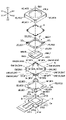
以下、本発明の実施形態に係る撮像素子駆動装置101について図面を参照して説明する。図1A及び図1Bは、撮像素子駆動装置101の斜視図である。具体的には、図1Aは、撮像素子駆動装置101の上方斜視図であり、図1Bは、撮像素子駆動装置101の下方斜視図である。図2は、撮像素子駆動装置101の分解斜視図である。
An imaging device driving device 101 according to an embodiment of the present invention will be described below with reference to the drawings. 1A and 1B are perspective views of the imaging device driving device 101. FIG. Specifically, FIG. 1A is a top perspective view of the imaging device driving device 101, and FIG. 1B is a bottom perspective view of the imaging device driving device 101. FIG. FIG. 2 is an exploded perspective view of the imaging device driving device 101. As shown in FIG.
図1A、図1B、及び図2において、X1は、三次元直交座標系を構成するX軸の一方向を表し、X2は、X軸の他方向を表す。また、Y1は、三次元直交座標系を構成するY軸の一方向を表し、Y2は、Y軸の他方向を表す。同様に、Z1は、三次元直交座標系を構成するZ軸の一方向を表し、Z2は、Z軸の他方向を表す。図1A、図1B、及び図2では、撮像素子駆動装置101のX1側は、撮像素子駆動装置101の前側(正面側)に相当し、撮像素子駆動装置101のX2側は、撮像素子駆動装置101の後側(背面側)に相当する。また、撮像素子駆動装置101のY1側は、撮像素子駆動装置101の左側に相当し、撮像素子駆動装置101のY2側は、撮像素子駆動装置101の右側に相当する。また、撮像素子駆動装置101のZ1側は、撮像素子駆動装置101の上側(被写体側)に相当し、撮像素子駆動装置101のZ2側は、撮像素子駆動装置101の下側(撮像素子側)に相当する。他の図においても同様である。
In Figures 1A, 1B, and 2, X1 represents one direction of the X-axis that constitutes the three-dimensional orthogonal coordinate system, and X2 represents the other direction of the X-axis. Y1 represents one direction of the Y-axis forming the three-dimensional orthogonal coordinate system, and Y2 represents the other direction of the Y-axis. Similarly, Z1 represents one direction of the Z-axis forming the three-dimensional orthogonal coordinate system, and Z2 represents the other direction of the Z-axis. 1A, 1B, and 2, the X1 side of the image pickup device driving device 101 corresponds to the front side (front side) of the image pickup device driving device 101, and the X2 side of the image pickup device driving device 101 corresponds to the image pickup device driving device. It corresponds to the rear side (back side) of 101 . The Y1 side of the imaging device driving device 101 corresponds to the left side of the imaging device driving device 101 , and the Y2 side of the imaging device driving device 101 corresponds to the right side of the imaging device driving device 101 . The Z1 side of the image pickup device driving device 101 corresponds to the upper side (object side) of the image pickup device driving device 101, and the Z2 side of the image pickup device driving device 101 corresponds to the lower side of the image pickup device driving device 101 (image pickup device side). corresponds to The same applies to other drawings.
撮像素子駆動装置101は、図1A、図1B、及び図2に示すように、固定側部材FBの一部であるカバー部材4を含む。
The imaging device driving device 101 includes a cover member 4 that is part of the fixed side member FB, as shown in FIGS. 1A, 1B, and 2 .
カバー部材4は、各部材を覆う筐体HSの一部として機能するように構成されている。本実施形態では、カバー部材4は、非磁性金属で形成されている。但し、カバー部材4は、磁性金属で形成されていてもよい。
The cover member 4 is configured to function as part of the housing HS that covers each member. In this embodiment, the cover member 4 is made of non-magnetic metal. However, the cover member 4 may be made of a magnetic metal.
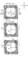
図1A及び図1Bに示す例では、カバー部材4は、矩形筒状の外周壁部4Aと、外周壁部4Aの上端(Z1側の端)と連続するように設けられた矩形環状且つ平板状の天板部4Bと、を有する。天板部4Bの中央には、円形の開口4kが形成されている。外周壁部4Aは、第1側板部4A1~第4側板部4A4を含む。第1側板部4A1と第3側板部4A3とは互いに対向し、第2側板部4A2と第4側板部4A4とは互いに対向している。そして、第1側板部4A1及び第3側板部4A3は、第2側板部4A2及び第4側板部4A4に対して垂直に延びている。
In the example shown in FIGS. 1A and 1B, the cover member 4 includes a rectangular tubular outer peripheral wall portion 4A and a rectangular annular flat plate shape provided so as to be continuous with the upper end (Z1 side end) of the outer peripheral wall portion 4A. and a top plate portion 4B. A circular opening 4k is formed in the center of the top plate portion 4B. The outer peripheral wall portion 4A includes a first side plate portion 4A1 to a fourth side plate portion 4A4. The first side plate portion 4A1 and the third side plate portion 4A3 face each other, and the second side plate portion 4A2 and the fourth side plate portion 4A4 face each other. The first side plate portion 4A1 and the third side plate portion 4A3 extend perpendicularly to the second side plate portion 4A2 and the fourth side plate portion 4A4.
カバー部材4は、図1A及び図1Bに示すように、接着剤によってベース部材8に接合されている。ベース部材8は、カバー部材4とともに筐体HSを構成している。
The cover member 4 is joined to the base member 8 with an adhesive, as shown in FIGS. 1A and 1B. The base member 8 constitutes a housing HS together with the cover member 4 .
筐体HS内には、図2に示すように、駆動部DM、撮像素子IS、撮像素子保持体2、金属部材5、弾性金属部材6、及び回路基板7等が収容されている。また、筐体HSを構成しているベース部材8の下面(Z2側の面)には可撓性基板3が取り付けられている。なお、図1Aでは、明瞭化のため、撮像素子ISにはクロスパターンが付され、可撓性基板3には粗いドットパターンが付され、回路基板7には細かいドットパターンが付されている。
As shown in FIG. 2, the housing HS accommodates the drive section DM, the image sensor IS, the image sensor holder 2, the metal member 5, the elastic metal member 6, the circuit board 7, and the like. A flexible substrate 3 is attached to the lower surface (surface on the Z2 side) of the base member 8 that constitutes the housing HS. In FIG. 1A, for the sake of clarity, the imaging element IS is provided with a cross pattern, the flexible substrate 3 is provided with a coarse dot pattern, and the circuit board 7 is provided with a fine dot pattern.
駆動部DMは、形状記憶アクチュエータの一例である形状記憶合金ワイヤSAを含む。本実施形態では、形状記憶合金ワイヤSAは、略同じ長さと略同じ直径を有する第1ワイヤSA1~第8ワイヤSA8を含む。形状記憶合金ワイヤSAは、電流が流れると温度が上昇し、その温度の上昇に応じて収縮する。駆動部DMは、形状記憶合金ワイヤSAの収縮を利用して撮像素子保持体2を移動させることができる。なお、形状記憶合金ワイヤSAは、第1ワイヤSA1~第8ワイヤSA8のうちの一つ又は複数が収縮すると撮像素子保持体2が移動し、その移動によって別の一つ又は複数が引き延ばされる(伸張される)ように構成されている。
The drive unit DM includes a shape memory alloy wire SA, which is an example of a shape memory actuator. In this embodiment, the shape memory alloy wires SA include first wires SA1 to eighth wires SA8 having substantially the same length and substantially the same diameter. The shape memory alloy wire SA increases in temperature when current flows, and contracts according to the increase in temperature. The drive unit DM can move the imaging element holder 2 using contraction of the shape memory alloy wires SA. As for the shape memory alloy wires SA, when one or more of the first wires SA1 to SA8 contract, the imaging device holder 2 moves, and the movement causes another one or more to be elongated. (decompressed).
本実施形態では、駆動部DMは、可動側部材MBの6自由度の動きを実現できるように構成されている。6自由度の動きは、撮像素子ISの撮像面に垂直な第1回転軸RX1に平行な第1方向(Z軸方向)における並進、第1方向に垂直な第2方向(X軸方向)における並進、第1方向及び第2方向に垂直な第3方向(Y軸方向)における並進、第1方向(Z軸方向)の周りの回転、第2方向(X軸方向)の周りの回転、並びに、第3方向(Y軸方向)の周りの回転を含む。なお、第2方向(X軸方向)は、第2回転軸RX2に平行な方向であり、第3方向(Y軸方向)は、第3回転軸RX3に平行な方向である。撮像素子ISの撮像面は、撮像素子ISの被写体側の面である上面と平行な面である。
In the present embodiment, the driving part DM is configured so that the movable side member MB can move with six degrees of freedom. The movements with six degrees of freedom are translation in a first direction (Z-axis direction) parallel to a first rotation axis RX1 perpendicular to the imaging surface of the image sensor IS, and movement in a second direction (X-axis direction) perpendicular to the first direction. translation, translation in a third direction (Y-axis direction) perpendicular to the first and second directions, rotation about the first direction (Z-axis direction), rotation about a second direction (X-axis direction), and , including rotation about a third direction (the Y-axis direction). The second direction (X-axis direction) is a direction parallel to the second rotation axis RX2, and the third direction (Y-axis direction) is a direction parallel to the third rotation axis RX3. The imaging surface of the imaging device IS is a plane parallel to the upper surface of the imaging device IS on the subject side.
可撓性基板3は、撮像素子駆動装置101と撮像素子駆動装置101の外部にある装置とを接続するための配線パターンが形成された可撓性の基板である。本実施形態では、可撓性基板3は、繰り返し変形させることができるように構成されたフレキシブルプリント回路基板である。
The flexible substrate 3 is a flexible substrate on which a wiring pattern is formed for connecting the imaging device driving device 101 and a device outside the imaging device driving device 101 . In this embodiment, the flexible substrate 3 is a flexible printed circuit board configured to be repeatedly deformable.
回路基板7は、撮像素子ISが搭載される基板である。本実施形態では、回路基板7は、リジット回路基板である。
The circuit board 7 is a board on which the imaging device IS is mounted. In this embodiment, the circuit board 7 is a rigid circuit board.
可動側部材MBは、駆動部DMによって駆動される部材である。本実施形態では、可動側部材MBは、撮像素子ISと、撮像素子ISが搭載される回路基板7と、回路基板7を保持可能な撮像素子保持体2とで構成されている。
The movable side member MB is a member that is driven by the drive section DM. In this embodiment, the movable-side member MB is composed of the image sensor IS, the circuit board 7 on which the image sensor IS is mounted, and the image sensor holder 2 capable of holding the circuit board 7 .
撮像素子保持体2は、液晶ポリマー(LCP)等の合成樹脂を射出成形することで形成されている。具体的には、撮像素子保持体2は、図2に示すように、上面視で略矩形の枠体2Fと、枠体2Fの四つの角部のうちの二つに形成された可動側台座部2Dと、枠体2Fの四つの角部のうちの残りの二つに形成された突設部2Sと、を含む。本実施形態では、回路基板7は、枠体2Fの下面に接着剤で接合されるように構成されている。
The imaging element holder 2 is formed by injection molding synthetic resin such as liquid crystal polymer (LCP). Specifically, as shown in FIG. 2, the imaging element holder 2 includes a frame 2F that is substantially rectangular in top view, and movable side pedestals formed at two of the four corners of the frame 2F. It includes a portion 2D and projecting portions 2S formed at the remaining two of the four corners of the frame 2F. In this embodiment, the circuit board 7 is configured to be bonded to the lower surface of the frame 2F with an adhesive.
可動側台座部2Dは、第1可動側台座部2D1及び第2可動側台座部2D2を含む。第1可動側台座部2D1及び第2可動側台座部2D2は、第1回転軸RX1を挟んで互いに対向するように配置されている。同様に、突設部2Sは、第1突設部2S1及び第2突設部2S2を含む。第1突設部2S1及び第2突設部2S2は、第1回転軸RX1を挟んで互いに対向するように配置されている。具体的には、可動側台座部2D及び突設部2Sは、上面視で略矩形状の外形を有する撮像素子保持体2(枠体2F)の四つの角部に対応するように配置され、且つ、交互に並ぶように配置されている。そして、二つの可動側台座部2Dのそれぞれには、図3に示すように、弾性金属部材6の一部が載置される。
The movable-side pedestal portion 2D includes a first movable-side pedestal portion 2D1 and a second movable-side pedestal portion 2D2. The first movable-side pedestal portion 2D1 and the second movable-side pedestal portion 2D2 are arranged so as to face each other with the first rotation axis RX1 interposed therebetween. Similarly, the projecting portion 2S includes a first projecting portion 2S1 and a second projecting portion 2S2. The first projecting portion 2S1 and the second projecting portion 2S2 are arranged to face each other with the first rotation axis RX1 interposed therebetween. Specifically, the movable-side pedestal portion 2D and the protruding portion 2S are arranged so as to correspond to the four corners of the imaging element holding body 2 (frame body 2F) having a substantially rectangular outer shape when viewed from above. Moreover, they are arranged so as to be alternately arranged. A part of the elastic metal member 6 is placed on each of the two movable-side pedestals 2D, as shown in FIG.
図3は、撮像素子保持体2とベース部材8とに接続された弾性金属部材6の斜視図であり、撮像素子保持体2及びベース部材8のそれぞれと弾性金属部材6との間の位置関係を示している。なお、図3では、明瞭化のため、撮像素子保持体2に細かいドットパターンが付され、ベース部材8に粗いドットパターンが付されている。また、図3では、明瞭化のため、撮像素子保持体2、弾性金属部材6、及びベース部材8以外の部材の図示が省略されている。
FIG. 3 is a perspective view of the elastic metal member 6 connected to the image pickup device holder 2 and the base member 8. The positional relationship between the image pickup device holder 2 and the base member 8 and the elastic metal member 6 is shown in FIG. is shown. In FIG. 3, for clarity, the imaging device holder 2 has a fine dot pattern and the base member 8 has a coarse dot pattern. 3, illustration of members other than the imaging element holder 2, the elastic metal member 6, and the base member 8 is omitted for clarity.
弾性金属部材6は、固定側部材FB(ベース部材8)に対して撮像素子保持体2を移動可能に支持できるように構成されている。本実施形態では、弾性金属部材6は、例えば、銅合金、チタン銅系合金(チタン銅)、又は銅ニッケル合金(ニッケルすず銅)等を主な材料とした導電性の金属板から作製されている。
The elastic metal member 6 is configured to movably support the imaging element holder 2 with respect to the fixed side member FB (base member 8). In this embodiment, the elastic metal member 6 is made of a conductive metal plate mainly made of, for example, a copper alloy, a titanium-copper alloy (titanium-copper), or a copper-nickel alloy (nickel-tin-copper). there is
ベース部材8は、液晶ポリマー(LCP)等の合成樹脂を用いた射出成形によって形成される。本実施形態では、ベース部材8は、図2に示すように、上面視で略矩形状の輪郭を有し、中央に開口8Kを有する。具体的には、ベース部材8は、開口8Kを囲むように配置される四つの辺部8E(第1辺部8E1~第4辺部8E4)を有する。
The base member 8 is formed by injection molding using synthetic resin such as liquid crystal polymer (LCP). In this embodiment, as shown in FIG. 2, the base member 8 has a substantially rectangular outline in top view and has an opening 8K in the center. Specifically, the base member 8 has four side portions 8E (first side portion 8E1 to fourth side portion 8E4) arranged to surround the opening 8K.
具体的には、ベース部材8は、図2に示すように、ベース部材8の四つの角部のうちの二つに形成された固定側台座部8Dを含む。固定側台座部8Dは、ベース部材8の板状の基部から上方(Z1方向)に突出している。そして、固定側台座部8Dは、第1固定側台座部8D1及び第2固定側台座部8D2を含む。第1固定側台座部8D1及び第2固定側台座部8D2は、第1回転軸RX1を挟んで互いに対向するように配置されている。また、図3に示すように、第1固定側台座部8D1は、撮像素子保持体2の第1突設部2S1と対向するように配置され、第2固定側台座部8D2は、撮像素子保持体2の第2突設部2S2と対向するように配置されている。
Specifically, the base member 8 includes fixed side pedestals 8D formed at two of the four corners of the base member 8, as shown in FIG. The fixed-side pedestal portion 8D protrudes upward (in the Z1 direction) from the plate-like base portion of the base member 8 . The fixed side pedestal portion 8D includes a first fixed side pedestal portion 8D1 and a second fixed side pedestal portion 8D2. The first fixed side seat portion 8D1 and the second fixed side seat portion 8D2 are arranged so as to face each other with the first rotation axis RX1 interposed therebetween. Further, as shown in FIG. 3, the first fixed side pedestal portion 8D1 is arranged so as to face the first projecting portion 2S1 of the image pickup element holder 2, and the second fixed side pedestal portion 8D2 is arranged to face the image pickup element holding portion 8D2. It is arranged so as to face the second projecting portion 2S2 of the body 2. As shown in FIG.
弾性金属部材6は、撮像素子保持体2に形成された可動側台座部2Dと、ベース部材8に形成された固定側台座部8Dとを繋ぐように構成されている。具体的には、弾性金属部材6は、図3に示すように、ベース部材8に形成された第1固定側台座部8D1に取り付けられる第1固定部6e1と、撮像素子保持体2に形成された第1可動側台座部2D1に取り付けられる第2固定部6e2と、ベース部材8に形成された第2固定側台座部8D2に取り付けられる第3固定部6e3と、撮像素子保持体2に形成された第2可動側台座部2D2に取り付けられる第4固定部6e4と、を有する。また、弾性金属部材6は、図3に示すように、第1固定部6e1と第2固定部6e2とを繋ぐ弾性変形可能な第1腕部6g1、第2固定部6e2と第3固定部6e3とを繋ぐ弾性変形可能な第2腕部6g2、第3固定部6e3と第4固定部6e4とを繋ぐ弾性変形可能な第3腕部6g3、及び、第4固定部6e4と第1固定部6e1とを繋ぐ弾性変形可能な第4腕部6g4を有する。
The elastic metal member 6 is configured to connect the movable-side pedestal portion 2D formed on the imaging element holder 2 and the fixed-side pedestal portion 8D formed on the base member 8 . Specifically, as shown in FIG. 3, the elastic metal member 6 includes a first fixed portion 6e1 attached to a first fixed-side pedestal portion 8D1 formed on the base member 8, and an elastic metal member 6 formed on the imaging element holder 2. a second fixed portion 6e2 attached to the first movable side pedestal portion 2D1; a third fixed portion 6e3 attached to the second fixed side pedestal portion 8D2 formed on the base member 8; and a fourth fixing portion 6e4 attached to the second movable side pedestal portion 2D2. As shown in FIG. 3, the elastic metal member 6 includes an elastically deformable first arm portion 6g1 connecting the first fixing portion 6e1 and the second fixing portion 6e2, a second fixing portion 6e2 and a third fixing portion 6e3. an elastically deformable second arm portion 6g2 that connects the third fixing portion 6e3 and the fourth fixing portion 6e4, and an elastically deformable third arm portion 6g3 that connects the fourth fixing portion 6e4 and the first fixing portion 6e1 It has an elastically deformable fourth arm portion 6g4 that connects the .
金属部材5は、形状記憶合金ワイヤSAの端部が固定されるように構成されている。本実施形態では、金属部材5は、図2に示すように、固定側金属部材5F及び可動側金属部材5Mを含む。固定側金属部材5Fは、ベース部材8の固定側台座部8Dに固定されるように構成されている。可動側金属部材5Mは、撮像素子保持体2の可動側台座部2Dに固定されるように構成されている。
The metal member 5 is configured so that the end of the shape memory alloy wire SA is fixed. In this embodiment, the metal member 5 includes a fixed side metal member 5F and a movable side metal member 5M, as shown in FIG. The stationary metal member 5</b>F is configured to be fixed to the stationary pedestal portion 8</b>D of the base member 8 . The movable-side metal member 5</b>M is configured to be fixed to the movable-side pedestal portion 2</b>D of the imaging element holder 2 .
より具体的には、固定側金属部材5Fは、固定側ターミナルプレートとも称され、第1固定側ターミナルプレート5F1~第8固定側ターミナルプレート5F8を含む。可動側金属部材5Mは、可動側ターミナルプレートとも称され、第1可動側ターミナルプレート5M1及び第2可動側ターミナルプレート5M2を含む。
More specifically, the fixed-side metal member 5F is also called a fixed-side terminal plate, and includes a first fixed-side terminal plate 5F1 to an eighth fixed-side terminal plate 5F8. The movable-side metal member 5M is also called a movable-side terminal plate, and includes a first movable-side terminal plate 5M1 and a second movable-side terminal plate 5M2.
次に、図4A及び図4Bを参照し、撮像素子保持体2及びベース部材8のそれぞれと金属部材5との間の位置関係について説明する。図4Aは、可動側金属部材5M(可動側ターミナルプレート)が取り付けられた撮像素子保持体2の斜視図である。図4Bは、固定側金属部材5F(固定側ターミナルプレート)が取り付けられたベース部材8の斜視図である。なお、明瞭化のため、図4Aでは、可動側金属部材5Mにドットパターンが付され、図4Bでは、固定側金属部材5Fにドットパターンが付されている。
Next, referring to FIGS. 4A and 4B, the positional relationship between each of the imaging element holder 2 and the base member 8 and the metal member 5 will be described. FIG. 4A is a perspective view of the imaging element holder 2 to which the movable-side metal member 5M (movable-side terminal plate) is attached. FIG. 4B is a perspective view of the base member 8 to which the fixed-side metal member 5F (fixed-side terminal plate) is attached. For clarity, in FIG. 4A, the movable metal member 5M has a dot pattern, and in FIG. 4B, the fixed metal member 5F has a dot pattern.
図4Aに示す例では、第1可動側ターミナルプレート5M1は、第1可動側台座部2D1のX1側の側壁(前側取付面)及びY1側の側壁(左側取付面)に固定されている。具体的には、第1可動側台座部2D1の上面に形成された溝部2G(図2参照。)と第1可動側ターミナルプレート5M1に形成された折り曲げ片BPとがかみ合った状態で、第1可動側ターミナルプレート5M1は、接着剤により第1可動側台座部2D1に固定されている。接着剤は、例えば、光硬化型接着剤である。光硬化型接着剤は、例えば、紫外線硬化型接着剤又は可視光硬化型接着剤等である。同様に、第2可動側ターミナルプレート5M2は、第2可動側台座部2D2のX2側の側壁(後側取付面)及びY2側の側壁(右側取付面)に固定されている。具体的には、第2可動側台座部2D2の上面に形成された溝部2G(図2参照。)と第2可動側ターミナルプレート5M2に形成された折り曲げ片BPとがかみ合った状態で、第2可動側ターミナルプレート5M2は、接着剤により第2可動側台座部2D2に固定されている。
In the example shown in FIG. 4A, the first movable terminal plate 5M1 is fixed to the X1 side wall (front mounting surface) and the Y1 side wall (left mounting surface) of the first movable pedestal portion 2D1. Specifically, in a state in which the groove 2G (see FIG. 2) formed on the upper surface of the first movable-side pedestal portion 2D1 and the bent piece BP formed on the first movable-side terminal plate 5M1 are engaged with each other, the first The movable terminal plate 5M1 is fixed to the first movable pedestal 2D1 with an adhesive. The adhesive is, for example, a photocurable adhesive. The photocurable adhesive is, for example, an ultraviolet curable adhesive or a visible light curable adhesive. Similarly, the second movable terminal plate 5M2 is fixed to the X2 side wall (rear mounting surface) and the Y2 side wall (right mounting surface) of the second movable pedestal portion 2D2. Specifically, in a state in which the groove 2G (see FIG. 2) formed on the upper surface of the second movable-side pedestal portion 2D2 and the bent piece BP formed on the second movable-side terminal plate 5M2 are engaged with each other, the second The movable terminal plate 5M2 is fixed to the second movable pedestal 2D2 with an adhesive.
図4Bに示す例では、第1固定側ターミナルプレート5F1及び第2固定側ターミナルプレート5F2は、ベース部材8の第1辺部8E1に沿って配置された第1固定側台座部8D1のX1側の側壁(前側取付面)に固定されている。具体的には、第1固定側ターミナルプレート5F1及び第2固定側ターミナルプレート5F2は、接着剤により第1固定側台座部8D1に固定されている。接着剤は、例えば、光硬化型接着剤である。光硬化型接着剤は、例えば、紫外線硬化型接着剤又は可視光硬化型接着剤等である。同様に、第3固定側ターミナルプレート5F3及び第4固定側ターミナルプレート5F4(図4Bでは不可視。)は、ベース部材8の第2辺部8E2に沿って配置された第2固定側台座部8D2のY1側の側壁(左側取付面)に固定されている。また、第5固定側ターミナルプレート5F5及び第6固定側ターミナルプレート5F6(図4Bでは不可視。)は、ベース部材8の第3辺部8E3に沿って配置された第2固定側台座部8D2のX2側の側壁(後側取付面)に固定されている。そして、第7固定側ターミナルプレート5F7及び第8固定側ターミナルプレート5F8は、ベース部材8の第4辺部8E4に沿って配置された第1固定側台座部8D1のY2側の側壁(右側取付面)に固定されている。
In the example shown in FIG. 4B, the first stationary terminal plate 5F1 and the second stationary terminal plate 5F2 are located on the X1 side of the first stationary seat 8D1 arranged along the first side 8E1 of the base member 8. It is fixed to the side wall (front mounting surface). Specifically, the first stationary terminal plate 5F1 and the second stationary terminal plate 5F2 are fixed to the first stationary pedestal portion 8D1 with an adhesive. The adhesive is, for example, a photocurable adhesive. The photocurable adhesive is, for example, an ultraviolet curable adhesive or a visible light curable adhesive. Similarly, the third stationary terminal plate 5F3 and the fourth stationary terminal plate 5F4 (not visible in FIG. 4B) are attached to the second stationary pedestal 8D2 arranged along the second side 8E2 of the base member 8 It is fixed to the side wall (left mounting surface) on the Y1 side. Also, the fifth fixed side terminal plate 5F5 and the sixth fixed side terminal plate 5F6 (not visible in FIG. 4B) are arranged along the third side 8E3 of the base member 8 on the X2 side of the second fixed side pedestal portion 8D2. side wall (rear mounting surface). The seventh stationary terminal plate 5F7 and the eighth stationary terminal plate 5F8 are arranged along the fourth side 8E4 of the base member 8 on the Y2 side wall (right mounting surface) of the first stationary pedestal 8D1. ).
形状記憶合金ワイヤSAは、カバー部材4の外周壁部4Aの内面に沿うように延びており、固定側部材FBに対して可動側部材MBを移動可能に支持できるように構成されている。本実施形態では、形状記憶合金ワイヤSAは、図2に示すように、第1ワイヤSA1~第8ワイヤSA8を含み、固定側部材FBとしてのベース部材8に対して、可動側部材MBとしての撮像素子保持体2を移動可能に支持できるように構成されている。具体的には、第1ワイヤSA1~第8ワイヤSA8のそれぞれは、図2に示すように、一端が圧着又は溶接等により固定側金属部材5Fに固着され、且つ、他端が圧着又は溶接等により可動側金属部材5Mに固着されている。
The shape memory alloy wire SA extends along the inner surface of the outer peripheral wall portion 4A of the cover member 4, and is configured to movably support the movable side member MB with respect to the fixed side member FB. In the present embodiment, the shape memory alloy wires SA include first wires SA1 to eighth wires SA8 as shown in FIG. It is configured to movably support the imaging device holder 2 . Specifically, as shown in FIG. 2, each of the first wire SA1 to the eighth wire SA8 has one end fixed to the stationary metal member 5F by crimping or welding, and the other end is crimped or welded. is fixed to the movable-side metal member 5M.
次に、図5A及び図5Bを参照し、形状記憶合金ワイヤSAが取り付けられる金属部材5について説明する。図5Aは、第2可動側ターミナルプレート5M2及び第7固定側ターミナルプレート5F7のそれぞれに取り付けられた第7ワイヤSA7、並びに、第2可動側ターミナルプレート5M2及び第8固定側ターミナルプレート5F8のそれぞれに取り付けられた第8ワイヤSA8をY2側(右側)から見たときの図である。図5Bは、第2可動側ターミナルプレート5M2及び第7固定側ターミナルプレート5F7のそれぞれに取り付けられた第7ワイヤSA7、並びに、第2可動側ターミナルプレート5M2及び第8固定側ターミナルプレート5F8のそれぞれに取り付けられた第8ワイヤSA8をX1側(前側)から見たときの図である。なお、図5A及び図5Bに示す各部材の位置関係は、撮像素子駆動装置101が組み立てられたときの位置関係に対応している。そして、図5A及び図5Bでは、明瞭化のため、他の部材の図示が省略されている。また、図5A及び図5Bを参照する以下の説明は、第7ワイヤSA7及び第8ワイヤSA8の組み合わせに関するが、第1ワイヤSA1及び第2ワイヤSA2の組み合わせ、第3ワイヤSA3及び第4ワイヤSA4の組み合わせ、並びに、第5ワイヤSA5及び第6ワイヤSA6の組み合わせについても同様に適用される。
Next, the metal member 5 to which the shape memory alloy wire SA is attached will be described with reference to FIGS. 5A and 5B. FIG. 5A shows a seventh wire SA7 attached to each of the second movable terminal plate 5M2 and the seventh fixed terminal plate 5F7, and a wire SA7 attached to each of the second movable terminal plate 5M2 and the eighth fixed terminal plate 5F8. It is a figure when the 8th wire SA8 attached is seen from the Y2 side (right side). FIG. 5B shows a seventh wire SA7 attached to each of the second movable side terminal plate 5M2 and the seventh fixed side terminal plate 5F7, and each of the second movable side terminal plate 5M2 and the eighth fixed side terminal plate 5F8. It is a figure when the 8th wire SA8 attached is seen from the X1 side (front side). Note that the positional relationship of each member shown in FIGS. 5A and 5B corresponds to the positional relationship when the imaging device driving device 101 is assembled. 5A and 5B, illustration of other members is omitted for clarity. Also, the following description with reference to FIGS. 5A and 5B relates to the combination of the seventh wire SA7 and the eighth wire SA8, the combination of the first wire SA1 and the second wire SA2, the third wire SA3 and the fourth wire SA4. and the combination of the fifth wire SA5 and the sixth wire SA6.
具体的には、第7ワイヤSA7の一端は、第7固定側ターミナルプレート5F7の保持部J2のところで第7固定側ターミナルプレート5F7に固定され、第7ワイヤSA7の他端は、第2可動側ターミナルプレート5M2の下側の保持部J1のところで第2可動側ターミナルプレート5M2に固定されている。同様に、第8ワイヤSA8の一端は、第8固定側ターミナルプレート5F8の保持部J4のところで第8固定側ターミナルプレート5F8に固定され、第8ワイヤSA8の他端は、第2可動側ターミナルプレート5M2の上側の保持部J3のところで第2可動側ターミナルプレート5M2に固定されている。
Specifically, one end of the seventh wire SA7 is fixed to the seventh fixed terminal plate 5F7 at the holding portion J2 of the seventh fixed terminal plate 5F7, and the other end of the seventh wire SA7 is fixed to the second movable terminal plate 5F7. It is fixed to the second movable side terminal plate 5M2 at the lower holding portion J1 of the terminal plate 5M2. Similarly, one end of the eighth wire SA8 is fixed to the eighth fixed terminal plate 5F8 at the holding portion J4 of the eighth fixed terminal plate 5F8, and the other end of the eighth wire SA8 is fixed to the second movable terminal plate. It is fixed to the second movable side terminal plate 5M2 at the upper holding portion J3 of 5M2.
保持部J1は、第2可動側ターミナルプレート5M2の一部を折り曲げることによって形成されている。具体的には、第2可動側ターミナルプレート5M2の一部は、第7ワイヤSA7の端部(他端)を挟み込んだ状態で折り曲げられることにより保持部J1を形成している。そして、第7ワイヤSA7の端部(他端)は、溶接によって保持部J1に固定されている。保持部J2~保持部J4についても同様である。
The holding portion J1 is formed by bending a portion of the second movable terminal plate 5M2. Specifically, a portion of the second movable terminal plate 5M2 forms a holding portion J1 by being bent while sandwiching the end (the other end) of the seventh wire SA7. An end (the other end) of the seventh wire SA7 is fixed to the holding portion J1 by welding. The same applies to the holding portions J2 to J4.
第7ワイヤSA7及び第8ワイヤSA8は、図5Aに示すように、互いにねじれの位置となるように(Y2側から見たときに立体的に交差するように)配置されている。すなわち、第7ワイヤSA7及び第8ワイヤSA8は、互いに接触しない(非接触となる)ように配置されている。
As shown in FIG. 5A, the seventh wire SA7 and the eighth wire SA8 are arranged so as to be twisted relative to each other (three-dimensionally intersect when viewed from the Y2 side). That is, the seventh wire SA7 and the eighth wire SA8 are arranged so as not to contact each other (become non-contact).
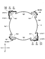
次に、図6を参照し、固定側部材FBの一部であるベース部材8の詳細について説明する。図6は、ベース部材8の斜視図である。具体的には、図6の上図は、導電部材CMが取り除かれた状態のベース部材8の斜視図であり、図6の中央図は、ベース部材8内に埋設されている導電部材CMの斜視図であり、図6の下図は、導電部材CMが埋設された状態のベース部材8の斜視図である。なお、図6の中央図及び図6の下図では、明瞭化のため、導電部材CMにドットパターンが付されている。
Next, with reference to FIG. 6, the details of the base member 8, which is a part of the fixed side member FB, will be described. 6 is a perspective view of the base member 8. FIG. Specifically, the upper view of FIG. 6 is a perspective view of the base member 8 with the conductive member CM removed, and the central view of FIG. 6 is a perspective view of the base member 8 in which the conductive member CM is embedded. In addition, in the central view of FIG. 6 and the lower view of FIG. 6, the conductive member CM is given a dot pattern for clarity.
ベース部材8は、第1ワイヤSA1~第8ワイヤSA8のそれぞれの一端を支持する固定側ワイヤ支持部として機能するように構成されている。また、撮像素子保持体2は、第1ワイヤSA1~第8ワイヤSA8のそれぞれの他端を支持する可動側ワイヤ支持部として機能するように構成されている。この構成により、可動側部材MBは、第1ワイヤSA1~第8ワイヤSA8によって固定側部材FBに対して6自由度で移動可能な状態で支持されている。
The base member 8 is configured to function as a fixed-side wire support section that supports one end of each of the first wire SA1 to the eighth wire SA8. Further, the imaging device holder 2 is configured to function as a movable side wire support section that supports the other ends of the first to eighth wires SA1 to SA8. With this configuration, the movable member MB is supported by the first wire SA1 to the eighth wire SA8 so as to be movable with respect to the fixed member FB with six degrees of freedom.
ベース部材8の被写体側の面(Z1側の面)である上面には、上述のように、固定側台座部8Dが形成されている。固定側台座部8Dは、第1固定側台座部8D1及び第2固定側台座部8D2を含む。第1固定側台座部8D1及び第2固定側台座部8D2は、第1回転軸RX1を挟んで対向するように配置されている。
As described above, the fixed side pedestal portion 8D is formed on the upper surface of the base member 8 on the subject side (Z1 side surface). The fixed side pedestal portion 8D includes a first fixed side pedestal portion 8D1 and a second fixed side pedestal portion 8D2. The first fixed side seat portion 8D1 and the second fixed side seat portion 8D2 are arranged to face each other with the first rotation axis RX1 interposed therebetween.
ベース部材8には、図6の中央図に示すような、銅、鉄、又はそれらを主成分とする合金等の材料を含む金属板から形成された導電部材CMがインサート成形によって埋め込まれている。本実施形態では、導電部材CMは、ベース部材8の下面(Z2側の面)に露出して外方に延びる接続部EDと、ベース部材8の固定側台座部8Dの上面(Z1側の面)に露出する接合面部CPと、を有するように構成されている。
In the base member 8, as shown in the central view of FIG. 6, a conductive member CM formed of a metal plate containing a material such as copper, iron, or an alloy containing them as a main component is embedded by insert molding. . In this embodiment, the conductive member CM includes a connecting portion ED exposed on the lower surface (Z2 side surface) of the base member 8 and extending outward, and an upper surface (Z1 side surface) of the fixed side pedestal portion 8D of the base member 8 (Z1 side surface). ).
具体的には、導電部材CMは、第1導電部材CM1及び第2導電部材CM2を含む。そして、第1導電部材CM1は、第1接続部ED1及び第1接合面部CP1を含み、第2導電部材CM2は、第2接続部ED2及び第2接合面部CP2を含む。
Specifically, the conductive member CM includes a first conductive member CM1 and a second conductive member CM2. The first conductive member CM1 includes a first connection portion ED1 and a first joint surface portion CP1, and the second conductive member CM2 includes a second connection portion ED2 and a second joint surface portion CP2.
次に、図7A及び図7Bを参照し、金属部材5、弾性金属部材6、導電部材CM、及び形状記憶合金ワイヤSAの位置関係について説明する。図7A及び図7Bは、金属部材5、弾性金属部材6、導電部材CM、及び形状記憶合金ワイヤSAの位置関係を示す図である。具体的には、図7Aは、各部材(金属部材5、弾性金属部材6、導電部材CM、及び形状記憶合金ワイヤSA)の斜視図であり、図7Bは、各部材の上面図である。なお、図7A及び図7Bでは、明瞭化のため、可動側金属部材5M及び導電部材CMにドットパターンが付されている。また、図7Bでは、明瞭化のため、形状記憶合金ワイヤSAの図示が省略されている。
Next, the positional relationship among the metal member 5, the elastic metal member 6, the conductive member CM, and the shape memory alloy wire SA will be described with reference to FIGS. 7A and 7B. 7A and 7B are diagrams showing the positional relationship among the metal member 5, the elastic metal member 6, the conductive member CM, and the shape memory alloy wire SA. Specifically, FIG. 7A is a perspective view of each member (metal member 5, elastic metal member 6, conductive member CM, and shape memory alloy wire SA), and FIG. 7B is a top view of each member. In addition, in FIGS. 7A and 7B, dot patterns are given to the movable-side metal member 5M and the conductive member CM for clarity. Also, in FIG. 7B, illustration of the shape memory alloy wire SA is omitted for clarity.
弾性金属部材6は、図3に示すように、ベース部材8の第1固定側台座部8D1(図2参照。)に固定される第1固定部6e1と、撮像素子保持体2の第1可動側台座部2D1(図2参照。)に固定される第2固定部6e2と、ベース部材8の第2固定側台座部8D2(図2参照。)に固定される第3固定部6e3と、撮像素子保持体2の第2可動側台座部2D2(図2参照。)に固定される第4固定部6e4と、第1固定部6e1と第2固定部6e2を繋ぐ第1腕部6g1と、第2固定部6e2と第3固定部6e3を繋ぐ第2腕部6g2と、第3固定部6e3と第4固定部6e4を繋ぐ第3腕部6g3と、第4固定部6e4と第1固定部6e1を繋ぐ第4腕部6g4と、を有する。
As shown in FIG. 3, the elastic metal member 6 includes a first fixed portion 6e1 fixed to the first fixed-side pedestal portion 8D1 (see FIG. 2) of the base member 8, and a first movable portion 6e1 of the imaging element holder 2. A second fixing portion 6e2 fixed to the side pedestal portion 2D1 (see FIG. 2), a third fixing portion 6e3 fixed to the second fixed side pedestal portion 8D2 (see FIG. 2) of the base member 8, and an imaging A fourth fixing portion 6e4 fixed to the second movable side pedestal portion 2D2 (see FIG. 2) of the element holder 2, a first arm portion 6g1 connecting the first fixing portion 6e1 and the second fixing portion 6e2, A second arm portion 6g2 connecting the second fixing portion 6e2 and the third fixing portion 6e3, a third arm portion 6g3 connecting the third fixing portion 6e3 and the fourth fixing portion 6e4, a fourth fixing portion 6e4 and the first fixing portion 6e1. and a fourth arm portion 6g4 that connects the
第1固定部6e1には、第1固定側台座部8D1に形成された上側に突出する円柱状の突出部8T(図4B参照。)が挿通される第1貫通孔6H1及び第2貫通孔6H2と、第1導電部材CM1の第1接合面部CP1(図6の下図参照。)との接合に用いられる第3貫通孔6H3とが形成されている。本実施形態では、弾性金属部材6と突出部8Tとの固定は、突出部8Tに熱かしめ又は冷間かしめを施すことによって実現される。但し、弾性金属部材6と突出部8Tとの固定は、接着剤によって実現されてもよい。また、本実施形態では、弾性金属部材6と第1導電部材CM1との接合は、レーザ溶接等の溶接によって実現される。但し、弾性金属部材6と第1導電部材CM1との接合は、半田又は導電性接着剤等によって実現されてもよい。
The first fixing portion 6e1 has a first through hole 6H1 and a second through hole 6H2 through which the upwardly protruding columnar protrusion 8T (see FIG. 4B) formed on the first fixed side pedestal portion 8D1 is inserted. , and a third through hole 6H3 used for bonding with the first bonding surface portion CP1 (see the lower diagram of FIG. 6) of the first conductive member CM1. In this embodiment, the fixing between the elastic metal member 6 and the projecting portion 8T is achieved by subjecting the projecting portion 8T to hot crimping or cold crimping. However, the fixing between the elastic metal member 6 and the projecting portion 8T may be realized by an adhesive. In addition, in the present embodiment, the elastic metal member 6 and the first conductive member CM1 are joined together by welding such as laser welding. However, the joint between the elastic metal member 6 and the first conductive member CM1 may be realized by solder, a conductive adhesive, or the like.
第2固定部6e2には、第1可動側台座部2D1に形成された上側に突出する円柱状の突出部2T(図4A参照。)が挿通される第4貫通孔6H4及び第5貫通孔6H5と、第1可動側ターミナルプレート5M1の折り曲げ片BP(図4A参照。)の先端との接合に用いられる第6貫通孔6H6とが形成されている。本実施形態では、弾性金属部材6と突出部2Tの固定は、突出部2Tに熱かしめ又は冷間かしめを施すことによって実現される。但し、弾性金属部材6と突出部2Tとの固定は、接着剤によって実現されてもよい。また、本実施形態では、弾性金属部材6と第1可動側ターミナルプレート5M1の折り曲げ片BPとの接合は、レーザ溶接等の溶接によって実現される。但し、弾性金属部材6と折り曲げ片BPとの接合は、半田又は導電性接着剤等によって実現されてもよい。
The second fixing portion 6e2 has a fourth through hole 6H4 and a fifth through hole 6H5 through which the upwardly projecting columnar protrusion 2T (see FIG. 4A) formed on the first movable side pedestal portion 2D1 is inserted. and a sixth through-hole 6H6 used for joining with the tip of the bent piece BP (see FIG. 4A) of the first movable-side terminal plate 5M1. In this embodiment, the fixing of the elastic metal member 6 and the projecting portion 2T is achieved by subjecting the projecting portion 2T to hot crimping or cold crimping. However, the fixing between the elastic metal member 6 and the projecting portion 2T may be realized by an adhesive. In addition, in this embodiment, the elastic metal member 6 and the bent piece BP of the first movable terminal plate 5M1 are joined together by welding such as laser welding. However, the joint between the elastic metal member 6 and the bent piece BP may be realized by solder, a conductive adhesive, or the like.
同様に、第3固定部6e3には、第2固定側台座部8D2に形成された上側に突出する円柱状の突出部8T(図4B参照。)が挿通される第7貫通孔6H7及び第8貫通孔6H8と、第2導電部材CM2の第2接合面部CP2(図6の下図参照。)との接合に用いられる第9貫通孔6H9とが形成されている。
Similarly, in the third fixing portion 6e3, a seventh through-hole 6H7 and an eighth through-hole 6H7 through which an upwardly protruding columnar projection 8T (see FIG. 4B) formed on the second fixed-side pedestal portion 8D2 is inserted. A through hole 6H8 and a ninth through hole 6H9 used for joining with the second joint surface portion CP2 (see the lower diagram of FIG. 6) of the second conductive member CM2 are formed.
また、第4固定部6e4には、第2可動側台座部2D2に形成された上側に突出する円柱状の突出部2T(図4A参照。)が挿通される第10貫通孔6H10及び第11貫通孔6H11と、第2可動側ターミナルプレート5M2の折り曲げ片BP(図4A参照。)の先端との接合に用いられる第12貫通孔6H12とが形成されている。
Further, in the fourth fixing portion 6e4, a tenth through-hole 6H10 and an eleventh through-hole 6H10 through which a cylindrical protrusion 2T (see FIG. 4A) protruding upward formed on the second movable side pedestal portion 2D2 is inserted. A hole 6H11 and a twelfth through hole 6H12 used for joining with the tip of the bent piece BP (see FIG. 4A) of the second movable terminal plate 5M2 are formed.
なお、弾性金属部材6の第1腕部6g1~第4腕部6g4のそれぞれは、四つの湾曲部を有する弾性変形可能な腕部である。そのため、撮像素子保持体2は、ベース部材8(固定側部材FB)に対して、第1回転軸RX1に平行な方向のみならず、第1回転軸RX1と交差する方向にも移動可能となっている。
Each of the first arm portion 6g1 to the fourth arm portion 6g4 of the elastic metal member 6 is an elastically deformable arm portion having four curved portions. Therefore, the imaging element holder 2 can move with respect to the base member 8 (fixed member FB) not only in the direction parallel to the first rotation axis RX1, but also in the direction intersecting the first rotation axis RX1. ing.
図7Bに示すように、弾性金属部材6は、第1回転軸RX1に対して2回回転対称となるように構成されている。そのため、弾性金属部材6は、撮像素子保持体2の重量バランスに悪影響を及ぼすことはほとんどない。また、弾性金属部材6は、八本の形状記憶合金ワイヤSA(第1ワイヤSA1~第8ワイヤSA8)によって支持される可動側部材MBの重量バランスに悪影響を及ぼすこともほとんどない。
As shown in FIG. 7B, the elastic metal member 6 is configured to have two-fold rotational symmetry with respect to the first rotation axis RX1. Therefore, the elastic metal member 6 hardly affects the weight balance of the image pickup device holder 2 . In addition, the elastic metal member 6 has almost no adverse effect on the weight balance of the movable side member MB supported by the eight shape memory alloy wires SA (first wire SA1 to eighth wire SA8).
固定側金属部材5Fは、接続部CT(図5A及び図5B参照。)を有し、接続部CTを介し、可撓性基板3の導電パターンPTに接合されるように構成されている。本実施形態では、接続部CTは、第1接続部CT1~第8接続部CT8を含む。
The fixed-side metal member 5F has a connection portion CT (see FIGS. 5A and 5B) and is configured to be joined to the conductive pattern PT of the flexible substrate 3 via the connection portion CT. In this embodiment, the connecting portion CT includes a first connecting portion CT1 to an eighth connecting portion CT8.
可撓性基板3は、図2に示すように、回路基板7の下面に取り付けられる略矩形状の内側部分3iと、ベース部材8の下面に取り付けられる略矩形環状の外側部分3eと、を含む。外側部分3eには、第1導電パターンPT1~第10導電パターンPT10が形成され、内側部分3iには、撮像素子ISとの接続に用いられる多数の導電パターン(図示せず。)が形成されている。なお、内側部分3iと外側部分3eとの間には、略U字状のスリット(開口)が形成されており、内側部分3iの動きが妨げられないように構成されている。
The flexible board 3 includes, as shown in FIG. 2, a substantially rectangular inner portion 3i attached to the lower surface of the circuit board 7 and a substantially rectangular annular outer portion 3e attached to the lower surface of the base member 8. . A first conductive pattern PT1 to a tenth conductive pattern PT10 are formed in the outer portion 3e, and a large number of conductive patterns (not shown) used for connection with the imaging element IS are formed in the inner portion 3i. there is A substantially U-shaped slit (opening) is formed between the inner portion 3i and the outer portion 3e so that the movement of the inner portion 3i is not hindered.
具体的には、第1固定側ターミナルプレート5F1の第1接続部CT1は、半田付けによって可撓性基板3の第1導電パターンPT1(図2参照。)に接合される。同様に、第2固定側ターミナルプレート5F2の第2接続部CT2は、半田付けによって可撓性基板3の第2導電パターンPT2(図2参照。)に接合され、第3固定側ターミナルプレート5F3の第3接続部CT3は、半田付けによって可撓性基板3の第3導電パターンPT3(図2参照。)に接合され、第4固定側ターミナルプレート5F4の第4接続部CT4は、半田付けによって可撓性基板3の第4導電パターンPT4(図2参照。)に接合され、第5固定側ターミナルプレート5F5の第5接続部CT5は、半田付けによって可撓性基板3の第5導電パターンPT5(図2参照。)に接合され、第6固定側ターミナルプレート5F6の第6接続部CT6は、半田付けによって可撓性基板3の第6導電パターンPT6(図2参照。)に接合され、第7固定側ターミナルプレート5F7の第7接続部CT7は、半田付けによって可撓性基板3の第7導電パターンPT7(図2参照。)に接合され、第8固定側ターミナルプレート5F8の第8接続部CT8は、半田付けによって可撓性基板3の第8導電パターンPT8(図2参照。)に接合される。なお、接続部CTと可撓性基板3の導電パターンPTとの接合は、導電性接着剤によって実現されてもよい。
Specifically, the first connecting portion CT1 of the first fixed-side terminal plate 5F1 is joined to the first conductive pattern PT1 (see FIG. 2) of the flexible substrate 3 by soldering. Similarly, the second connection portion CT2 of the second fixed terminal plate 5F2 is soldered to the second conductive pattern PT2 (see FIG. 2) of the flexible substrate 3, and the third fixed terminal plate 5F3 is The third connection portion CT3 is joined to the third conductive pattern PT3 (see FIG. 2) of the flexible substrate 3 by soldering, and the fourth connection portion CT4 of the fourth fixed terminal plate 5F4 is soldered. It is joined to the fourth conductive pattern PT4 (see FIG. 2) of the flexible substrate 3, and the fifth connecting portion CT5 of the fifth fixed-side terminal plate 5F5 is soldered to the fifth conductive pattern PT5 (see FIG. 2) of the flexible substrate 3. 2), and the sixth connecting portion CT6 of the sixth fixed terminal plate 5F6 is joined to the sixth conductive pattern PT6 (see FIG. 2) of the flexible substrate 3 by soldering, and the seventh The seventh connecting portion CT7 of the fixed terminal plate 5F7 is soldered to the seventh conductive pattern PT7 (see FIG. 2) of the flexible substrate 3, and the eighth connecting portion CT8 of the eighth fixed terminal plate 5F8 is connected. is joined to the eighth conductive pattern PT8 (see FIG. 2) of the flexible substrate 3 by soldering. Note that the connecting portion CT and the conductive pattern PT of the flexible substrate 3 may be joined by a conductive adhesive.
第1導電部材CM1の第1接続部ED1は、半田付けによって可撓性基板3の第9導電パターンPT9(図2参照。)に接合され、第2導電部材CM2の第2接続部ED2は、半田付けによって可撓性基板3の第10導電パターンPT10(図2参照。)に接合される。本実施形態では、第9導電パターンPT9及び第10導電パターンPT10は何れも接地端子(図示せず。)に接続されている。なお、接続部EDと可撓性基板3の導電パターンPTとの接合は、導電性接着剤によって実現されてもよい。
The first connection portion ED1 of the first conductive member CM1 is soldered to the ninth conductive pattern PT9 (see FIG. 2) of the flexible substrate 3, and the second connection portion ED2 of the second conductive member CM2 is It is joined to the tenth conductive pattern PT10 (see FIG. 2) of the flexible substrate 3 by soldering. In this embodiment, both the ninth conductive pattern PT9 and the tenth conductive pattern PT10 are connected to a ground terminal (not shown). Note that the connection portion ED and the conductive pattern PT of the flexible substrate 3 may be joined by a conductive adhesive.
第1可動側ターミナルプレート5M1の折り曲げ片BPは、図7Bに示すように、レーザ溶接等の溶接によって弾性金属部材6の第2固定部6e2に接合される。同様に、第2可動側ターミナルプレート5M2の折り曲げ片BPは、レーザ溶接等の溶接によって弾性金属部材6の第4固定部6e4に接合される。
The bent piece BP of the first movable terminal plate 5M1 is joined to the second fixed portion 6e2 of the elastic metal member 6 by welding such as laser welding, as shown in FIG. 7B. Similarly, the bent piece BP of the second movable side terminal plate 5M2 is joined to the fourth fixed portion 6e4 of the elastic metal member 6 by welding such as laser welding.
第1固定側ターミナルプレート5F1、第2固定側ターミナルプレート5F2、第7固定側ターミナルプレート5F7、及び第8固定側ターミナルプレート5F8は、図7Bに示すように、弾性金属部材6の第1固定部6e1から離間して配置されており、弾性金属部材6の第1固定部6e1には接触していない。一方で、弾性金属部材6の第1固定部6e1は、図7Bに示すように、レーザ溶接等の溶接によって第1導電部材CM1の第1接合面部CP1に接合されている。同様に、第3固定側ターミナルプレート5F3~第6固定側ターミナルプレート5F6は、図7Bに示すように、弾性金属部材6の第3固定部6e3から離間して配置されており、弾性金属部材6の第3固定部6e3には接触していない。一方で、弾性金属部材6の第3固定部6e3は、図7Bに示すように、レーザ溶接等の溶接によって第2導電部材CM2の第2接合面部CP2に接合されている。
The first stationary terminal plate 5F1, the second stationary terminal plate 5F2, the seventh stationary terminal plate 5F7, and the eighth stationary terminal plate 5F8 are the first stationary portion of the elastic metal member 6, as shown in FIG. 7B. 6e1, and is not in contact with the first fixing portion 6e1 of the elastic metal member 6. As shown in FIG. On the other hand, as shown in FIG. 7B, the first fixed portion 6e1 of the elastic metal member 6 is joined to the first joint surface portion CP1 of the first conductive member CM1 by welding such as laser welding. Similarly, the third stationary terminal plate 5F3 to the sixth stationary terminal plate 5F6 are arranged apart from the third stationary portion 6e3 of the elastic metal member 6, as shown in FIG. 7B. is not in contact with the third fixing portion 6e3. On the other hand, as shown in FIG. 7B, the third fixing portion 6e3 of the elastic metal member 6 is joined to the second joint surface portion CP2 of the second conductive member CM2 by welding such as laser welding.
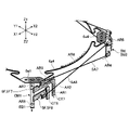
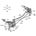
次に、図8A及び図8Bを参照し、形状記憶合金ワイヤSAを流れる電流の経路について説明する。図8A及び図8Bは、図7Aに示す構成の一部の斜視図である。なお、図8A及び図8Bでは、明瞭化のため、第1導電部材CM1及び第2可動側ターミナルプレート5M2には粗いドットパターンが付され、第7固定側ターミナルプレート5F7及び第8固定側ターミナルプレート5F8には細かいドットパターンが付され、弾性金属部材6には更に細かいドットパターンが付されている。
Next, with reference to FIGS. 8A and 8B, the path of current flowing through the shape memory alloy wire SA will be described. 8A and 8B are perspective views of a portion of the arrangement shown in FIG. 7A. In FIGS. 8A and 8B, for clarity, the first conductive member CM1 and the second movable terminal plate 5M2 are given rough dot patterns, and the seventh stationary terminal plate 5F7 and the eighth stationary terminal plate 5F8 has a fine dot pattern, and the elastic metal member 6 has an even finer dot pattern.
具体的には、図8Aは、第7固定側ターミナルプレート5F7の第7接続部CT7が高電位に接続され、且つ、第1導電部材CM1の第1接続部ED1が低電位に接続されたときの電流の経路を示し、図8Bは、第8固定側ターミナルプレート5F8の第8接続部CT8が高電位に接続され、且つ、第1導電部材CM1の第1接続部ED1が低電位に接続されたときの電流の経路を示す。以下の説明は、第7ワイヤSA7又は第8ワイヤSA8を流れる電流の経路に関するが、第1ワイヤSA1又は第2ワイヤSA2を流れる電流の経路、第3ワイヤSA3又は第4ワイヤSA4を流れる電流の経路、及び、第5ワイヤSA5又は第6ワイヤSA6を流れる電流の経路についても同様に適用される。
Specifically, FIG. 8A shows the state when the seventh connection portion CT7 of the seventh stationary terminal plate 5F7 is connected to a high potential and the first connection portion ED1 of the first conductive member CM1 is connected to a low potential. FIG. 8B shows that the eighth connection portion CT8 of the eighth fixed terminal plate 5F8 is connected to a high potential, and the first connection portion ED1 of the first conductive member CM1 is connected to a low potential. shows the path of the current when The following description relates to the path of the current flowing through the seventh wire SA7 or the eighth wire SA8, but the path of the current flowing through the first wire SA1 or the second wire SA2, the current flowing through the third wire SA3 or the fourth wire SA4. The same applies to the path and the path of the current flowing through the fifth wire SA5 or the sixth wire SA6.
第7固定側ターミナルプレート5F7の第7接続部CT7が高電位に接続され、且つ、第1導電部材CM1の第1接続部ED1が低電位に接続されると、電流は、図8Aの矢印AR1で示すように第7接続部CT7を通って第7固定側ターミナルプレート5F7に流れる。その後、電流は、矢印AR2で示すように第7固定側ターミナルプレート5F7を通り、矢印AR3で示すように第7ワイヤSA7を通り、更に、矢印AR4で示すように第2可動側ターミナルプレート5M2を通る。その後、電流は、矢印AR5、矢印AR6、及び矢印AR7で示すように弾性金属部材6の第4固定部6e4、第4腕部6g4、及び第1固定部6e1を通り、そして、矢印AR8で示すように第1導電部材CM1を通って第1接続部ED1に流れる。
When the seventh connecting portion CT7 of the seventh stationary terminal plate 5F7 is connected to a high potential and the first connecting portion ED1 of the first conductive member CM1 is connected to a low potential, the current flows as indicated by the arrow AR1 in FIG. 8A. flows through the seventh connecting portion CT7 to the seventh stationary terminal plate 5F7. After that, the current flows through the seventh fixed terminal plate 5F7 as indicated by arrow AR2, through the seventh wire SA7 as indicated by arrow AR3, and further through the second movable terminal plate 5M2 as indicated by arrow AR4. pass. Thereafter, the current flows through the fourth fixing portion 6e4, the fourth arm portion 6g4 and the first fixing portion 6e1 of the elastic metal member 6 as indicated by arrows AR5, AR6 and AR7, and then through the first fixing portion 6e1 as indicated by arrow AR8. flows through the first conductive member CM1 to the first connecting portion ED1.
なお、本実施形態では、電流は、弾性金属部材6の第4固定部6e4、第3腕部6g3、第3固定部6e3、第2導電部材CM2を通って第2接続部ED2にも流れるように構成されている。第1導電部材CM1の第1接続部ED1と第2導電部材CM2の第2接続部ED2とは何れも接地されているためである。
In this embodiment, the current flows through the fourth fixing portion 6e4 of the elastic metal member 6, the third arm portion 6g3, the third fixing portion 6e3, the second conductive member CM2, and also the second connecting portion ED2. is configured to This is because both the first connection portion ED1 of the first conductive member CM1 and the second connection portion ED2 of the second conductive member CM2 are grounded.
第8固定側ターミナルプレート5F8の第8接続部CT8が高電位に接続され、且つ、第1導電部材CM1の第1接続部ED1が低電位に接続されると、電流は、図8Bの矢印AR11で示すように第8接続部CT8を通って第8固定側ターミナルプレート5F8に流れる。その後、電流は、矢印AR12で示すように第8固定側ターミナルプレート5F8を通り、矢印AR13で示すように第8ワイヤSA8を通り、更に、矢印AR14で示すように第2可動側ターミナルプレート5M2を通る。その後、電流は、矢印AR15、矢印AR16、及び矢印AR17で示すように弾性金属部材6の第4固定部6e4、第4腕部6g4、及び第1固定部6e1を通り、そして、矢印AR18で示すように第1導電部材CM1を通って第1接続部ED1に流れる。
When the eighth connecting portion CT8 of the eighth fixed-side terminal plate 5F8 is connected to a high potential and the first connecting portion ED1 of the first conductive member CM1 is connected to a low potential, the current flows as indicated by the arrow AR11 in FIG. 8B. , flows through the eighth connecting portion CT8 to the eighth stationary terminal plate 5F8. After that, the current flows through the eighth fixed terminal plate 5F8 as indicated by arrow AR12, the eighth wire SA8 as indicated by arrow AR13, and the second movable terminal plate 5M2 as indicated by arrow AR14. pass. After that, the current flows through the fourth fixing portion 6e4, the fourth arm portion 6g4 and the first fixing portion 6e1 of the elastic metal member 6 as indicated by arrows AR15, AR16 and AR17, and then through the first fixing portion 6e1 as indicated by arrow AR18. flows through the first conductive member CM1 to the first connecting portion ED1.
なお、本実施形態では、電流は、弾性金属部材6の第4固定部6e4、第3腕部6g3、第3固定部6e3、第2導電部材CM2を通って第2接続部ED2にも流れるように構成されている。第1導電部材CM1の第1接続部ED1と第2導電部材CM2の第2接続部ED2とは何れも接地されているためである。
In this embodiment, the current flows through the fourth fixing portion 6e4 of the elastic metal member 6, the third arm portion 6g3, the third fixing portion 6e3, the second conductive member CM2, and also the second connecting portion ED2. is configured to This is because both the first connection portion ED1 of the first conductive member CM1 and the second connection portion ED2 of the second conductive member CM2 are grounded.
また、第7固定側ターミナルプレート5F7の第7接続部CT7が高電位に接続された場合、及び、第8固定側ターミナルプレート5F8の第8接続部CT8が高電位に接続された場合の何れにおいても、第2可動側ターミナルプレート5M2を通過した後の電流の経路は同じである。
Also, when the seventh connecting portion CT7 of the seventh fixed terminal plate 5F7 is connected to a high potential, or when the eighth connecting portion CT8 of the eighth fixed side terminal plate 5F8 is connected to a high potential, , the path of the current after passing through the second movable-side terminal plate 5M2 is the same.
上述のような撮像素子駆動装置101の外部にある制御装置は、第1固定側ターミナルプレート5F1~第8固定側ターミナルプレート5F8のそれぞれの接続部CTに印加される電圧を制御することにより、第1ワイヤSA1~第8ワイヤSA8のそれぞれの伸縮を制御できる。或いは、制御装置は、第1固定側ターミナルプレート5F1~第8固定側ターミナルプレート5F8のそれぞれの接続部CTと第1導電部材CM1及び第2導電部材CM2のそれぞれの接続部EDとを介して第1ワイヤSA1~第8ワイヤSA8のそれぞれに供給される電流を制御することにより、第1ワイヤSA1~第8ワイヤSA8のそれぞれの伸縮を制御できる。なお、制御装置は、撮像素子駆動装置101内に配置されていてもよい。また、制御装置は、撮像素子駆動装置101の構成要素であってもよい。
A control device external to the imaging device driving device 101 as described above controls the voltages applied to the respective connection portions CT of the first fixed-side terminal plate 5F1 to the eighth fixed-side terminal plate 5F8, thereby The expansion and contraction of each of the 1st wire SA1 to the 8th wire SA8 can be controlled. Alternatively, the control device controls the first terminal plate 5F1 through the eighth fixed terminal plate 5F8 via the connecting portions CT of the first to eighth stationary terminal plates 5F8 and the connecting portions ED of the first conductive member CM1 and the second conductive member CM2. By controlling the current supplied to each of the first wire SA1 to the eighth wire SA8, the expansion and contraction of each of the first wire SA1 to the eighth wire SA8 can be controlled. Note that the control device may be arranged in the imaging device driving device 101 . Also, the control device may be a component of the imaging device driving device 101 .
略直方体形状を有する撮像素子駆動装置101は、例えば、レンズ体、プリズム、又はミラー等の光学素子(図示せず。)と撮像素子ISとが対向するように、別の基板(図示せず。)の上に取り付けられる。カメラモジュールは、例えば、撮像素子ISと、撮像素子駆動装置101と、撮像素子ISに対向するレンズ体とで構成される。カメラモジュールは、制御装置を含んでいてもよい。また、光学素子としてのレンズ体は、撮像素子駆動装置101に取り付けられていてもよい。例えば、レンズ体は、筐体HSを構成するカバー部材4の開口4kに固定されていてもよい。この場合、レンズ体の光軸は、撮像素子保持体2が中立位置(初期状態)にあるときの第1回転軸RX1と一致している。
The image pickup device driving device 101 having a substantially rectangular parallelepiped shape is mounted on another substrate (not shown) such that an optical device (not shown) such as a lens body, a prism, or a mirror faces the image pickup device IS. ). The camera module includes, for example, an image sensor IS, an image sensor driving device 101, and a lens body facing the image sensor IS. A camera module may include a controller. Also, the lens body as an optical element may be attached to the imaging device driving device 101 . For example, the lens body may be fixed to the opening 4k of the cover member 4 forming the housing HS. In this case, the optical axis of the lens body coincides with the first rotation axis RX1 when the imaging element holder 2 is in the neutral position (initial state).
制御装置は、例えば、駆動部DMとしての形状記憶合金ワイヤSAの収縮による第1回転軸RX1に平行な第1方向(Z軸方向)に沿った駆動力を利用し、レンズ体のZ2側において、第1方向に沿って撮像素子保持体2を移動させてもよい。そして、このように撮像素子保持体2を移動させることにより、制御装置は、レンズ調整機能の一つである自動焦点調整機能を実現してもよい。具体的には、制御装置は、レンズ体から離れる方向に撮像素子保持体2を移動させてマクロ撮影を可能にし、レンズ体に近づく方向に撮像素子保持体2を移動させて無限遠撮影を可能にしてもよい。
The control device utilizes, for example, a driving force along a first direction (Z-axis direction) parallel to the first rotation axis RX1 due to contraction of the shape memory alloy wire SA as the drive unit DM, and on the Z2 side of the lens body , the imaging element holder 2 may be moved along the first direction. By moving the image sensor holder 2 in this manner, the control device may realize an automatic focus adjustment function, which is one of the lens adjustment functions. Specifically, the control device moves the image sensor holder 2 in a direction away from the lens body to enable macro photography, and moves the image sensor holder 2 in a direction to approach the lens body to enable infinity photography. can be
また、制御装置は、複数の形状記憶合金ワイヤSAに流れる電流を制御することによって、第1方向と交差する方向に撮像素子保持体2を移動させてもよい。第1方向と交差する方向は、例えば、第1方向に垂直な第2方向(X軸方向)、又は、第1方向及び第2方向に垂直な第3方向(Y軸方向)であってもよい。また、制御装置は、第1方向(Z軸方向)の周り、第2方向(X軸方向)の周り、又は、第3方向(Y軸方向)の周りで撮像素子保持体2を回転させてもよい。このような撮像素子保持体2の動きにより、制御装置は、手振れ補正機能を実現してもよい。
The control device may also move the imaging element holder 2 in a direction intersecting with the first direction by controlling the currents flowing through the plurality of shape memory alloy wires SA. The direction intersecting the first direction is, for example, the second direction (X-axis direction) perpendicular to the first direction, or the third direction (Y-axis direction) perpendicular to the first direction and the second direction. good. In addition, the control device rotates the imaging element holder 2 around the first direction (Z-axis direction), around the second direction (X-axis direction), or around the third direction (Y-axis direction). good too. By such movement of the image pickup device holder 2, the control device may implement a camera shake correction function.
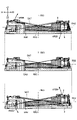
次に、図9~図16を参照し、駆動部DMの詳細について説明する。図9は、撮像素子保持体2の6自由度の動きのそれぞれを実現する際の形状記憶合金ワイヤSAの伸縮状態を示す表である。図10は、形状記憶合金ワイヤSAによって連結された撮像素子保持体2とベース部材8の上面図、正面図、背面図、左側面図、及び右側面図である。図11は、ベース部材8に対してX軸方向に並進する撮像素子保持体2とベース部材8の上面図である。図12は、ベース部材8に対してY軸方向に並進する撮像素子保持体2とベース部材8の上面図である。図13は、ベース部材8に対してZ軸方向に並進する撮像素子保持体2とベース部材8の正面図である。図14は、X軸(第2回転軸RX2)の周りで回転する撮像素子保持体2とベース部材8の正面図である。図15は、Y軸(第3回転軸RX3)の周りで回転する撮像素子保持体2とベース部材8の右側面図である。図16は、Z軸(第1回転軸RX1)の周りで回転する撮像素子保持体2とベース部材8の上面図である。なお、図10~図16では、明瞭化のため、撮像素子保持体2に細かいドットパターンが付され、ベース部材8に粗いドットパターンが付されている。
Next, the details of the drive unit DM will be described with reference to FIGS. 9 to 16. FIG. FIG. 9 is a table showing expansion and contraction states of the shape memory alloy wire SA when realizing each of the six degrees of freedom of movement of the imaging element holder 2 . 10A and 10B are a top view, a front view, a rear view, a left side view, and a right side view of the imaging element holder 2 and the base member 8 which are connected by the shape memory alloy wire SA. FIG. 11 is a top view of the imaging element holder 2 and the base member 8 that translate in the X-axis direction with respect to the base member 8. FIG. FIG. 12 is a top view of the imaging element holder 2 and the base member 8 that translate in the Y-axis direction with respect to the base member 8. FIG. FIG. 13 is a front view of the imaging element holder 2 and the base member 8 that translate in the Z-axis direction with respect to the base member 8. FIG. FIG. 14 is a front view of the imaging element holder 2 and the base member 8 rotating around the X-axis (second rotation axis RX2). FIG. 15 is a right side view of the imaging element holder 2 and the base member 8 rotating around the Y-axis (third rotation axis RX3). FIG. 16 is a top view of the imaging element holder 2 and the base member 8 rotating around the Z-axis (first rotation axis RX1). 10 to 16, for clarity, the imaging element holder 2 has a fine dot pattern and the base member 8 has a coarse dot pattern.
図10は、撮像素子駆動装置101が中立状態(中立位置)にあるときの撮像素子保持体2、ベース部材8、及び形状記憶合金ワイヤSAの状態を示す。なお、撮像素子駆動装置101の中立状態は、固定側部材FBに対して、X軸、Y軸、及びZ軸のそれぞれの方向に沿って並進可能な撮像素子保持体2がX軸方向における移動可能範囲の中間に位置し、Y軸方向における移動可能範囲の中間に位置し、且つ、Z軸方向における移動可能範囲の中間に位置している状態を意味する。典型的には、撮像素子駆動装置101の中立状態では、撮像素子保持体2は、X軸方向、Y軸方向、及びZ軸方向におけるそれぞれの移動可能範囲の中央に位置している状態にある。また、撮像素子駆動装置101の中立状態は、X軸(第2回転軸RX2)の周り、Y軸(第3回転軸RX3)の周り、及び、Z軸(第1回転軸RX1)の周りにそれぞれ回転可能(揺動可能)な撮像素子保持体2がそれぞれの回転軸周りの回転可能範囲(回転可能角度)の中間に位置している状態を意味する。典型的には、撮像素子駆動装置101の中立状態では、撮像素子ISの撮像面は、撮像素子ISに対向配置されるレンズ体の光軸と垂直な状態である。この場合、撮像素子IS(撮像面)の中心軸である第1回転軸RX1は、レンズ体の光軸に一致している。なお、形状記憶合金ワイヤSAに電流が供給されていないときの撮像素子駆動装置101の初期状態を中立状態としてもよい。
FIG. 10 shows the state of the imaging element holder 2, the base member 8, and the shape memory alloy wire SA when the imaging element driving device 101 is in a neutral state (neutral position). Note that the neutral state of the image pickup device driving device 101 means that the image pickup device holder 2, which is translatable along each of the X-axis, Y-axis, and Z-axis directions with respect to the fixed-side member FB, moves in the X-axis direction. It means a state of being positioned in the middle of the possible range, in the middle of the movable range in the Y-axis direction, and in the middle of the movable range in the Z-axis direction. Typically, in the neutral state of the image pickup device driving device 101, the image pickup device holder 2 is positioned at the center of each movable range in the X-axis direction, the Y-axis direction, and the Z-axis direction. . Further, the neutral state of the imaging device driving device 101 is around the X axis (second rotation axis RX2), around the Y axis (third rotation axis RX3), and around the Z axis (first rotation axis RX1). It means a state in which each rotatable (swingable) imaging element holder 2 is positioned in the middle of the rotatable range (rotatable angle) around each rotation axis. Typically, in the neutral state of the image pickup device driving device 101, the image pickup surface of the image pickup device IS is perpendicular to the optical axis of the lens body arranged to face the image pickup device IS. In this case, the first rotation axis RX1, which is the central axis of the imaging element IS (imaging surface), coincides with the optical axis of the lens body. Note that the initial state of the imaging device driving device 101 when no current is supplied to the shape memory alloy wires SA may be the neutral state.
具体的には、撮像素子駆動装置101が中立状態にあるとき、第2ワイヤSA2は、Z1側から見た上面視において、その一端(固定端)がその他端(可動端)よりも所定距離D1だけ外側(前側(X1側))に位置するように配置されている。なお、第2ワイヤSA2の一端(固定端)は、第2固定側ターミナルプレート5F2に固定される端部であり、第2ワイヤSA2の他端(可動端)は、第1可動側ターミナルプレート5M1に固定される端部である。
Specifically, when the image pickup device driving device 101 is in the neutral state, one end (fixed end) of the second wire SA2 is positioned further by a predetermined distance D1 than the other end (movable end) in a top view from the Z1 side. It is arranged so as to be located on the outer side (front side (X1 side)). One end (fixed end) of the second wire SA2 is the end fixed to the second fixed terminal plate 5F2, and the other end (movable end) of the second wire SA2 is the first movable terminal plate 5M1. is the end that is fixed to the
また、上面視において、第4ワイヤSA4は、その一端(固定端)がその他端(可動端)よりも所定距離D2だけ外側(左側(Y1側))に位置するように配置され、第6ワイヤSA6は、その一端(固定端)がその他端(可動端)よりも所定距離D3だけ外側(後側(X2側))に位置するように配置され、第8ワイヤSA8は、その一端(固定端)がその他端(可動端)よりも所定距離D4だけ外側(右側(Y2側))に位置するように配置されている。第1ワイヤSA1、第3ワイヤSA3、第5ワイヤSA5、及び第7ワイヤSA7についても同様である。
In addition, the fourth wire SA4 is arranged such that one end (fixed end) thereof is positioned outside (to the left (Y1 side)) the other end (movable end) of the fourth wire SA4 by a predetermined distance D2 when viewed from the top. One end (fixed end) of SA6 is positioned outside (rear side (X2 side)) a predetermined distance D3 from the other end (movable end). ) is positioned outside (to the right (Y2 side)) of the other end (movable end) by a predetermined distance D4. The same applies to the first wire SA1, the third wire SA3, the fifth wire SA5, and the seventh wire SA7.
すなわち、上面視において、第1ワイヤSA1、第2ワイヤSA2、第5ワイヤSA5、及び第6ワイヤSA6は、Y軸に対して非平行となるように配置され、第3ワイヤSA3、第4ワイヤSA4、第7ワイヤSA7、及び第8ワイヤSA8は、X軸に対して非平行となるように配置されている。
That is, when viewed from above, the first wire SA1, the second wire SA2, the fifth wire SA5, and the sixth wire SA6 are arranged so as to be non-parallel to the Y-axis, and the third wire SA3 and the fourth wire SA3 are arranged to be non-parallel to the Y axis. SA4, seventh wire SA7, and eighth wire SA8 are arranged so as to be non-parallel to the X-axis.
このような配置により、制御装置は、例えば、第1ワイヤSA1~第8ワイヤSA8の一部を収縮させ、且つ、残りを伸張させることにより、撮像素子保持体2をX軸又はY軸に沿って並進させることができる。
With such an arrangement, the control device can move the image sensor holder 2 along the X-axis or the Y-axis, for example, by contracting a part of the first wire SA1 to the eighth wire SA8 and extending the rest. can be translated by
また、撮像素子駆動装置101が中立状態にあるとき、X1側から見た正面視において、第1ワイヤSA1は、その一端(固定端)がその他端(可動端)よりも高い位置となるように配置され、第2ワイヤSA2は、その一端(固定端)がその他端(可動端)よりも低い位置となるように配置され、更に、第1ワイヤSA1と第2ワイヤSA2とは交差するように配置されている。
In addition, when the imaging device driving device 101 is in a neutral state, the first wire SA1 is arranged such that one end (fixed end) thereof is positioned higher than the other end (movable end) in a front view viewed from the X1 side. The second wire SA2 is arranged so that one end (fixed end) is lower than the other end (movable end), and the first wire SA1 and the second wire SA2 are arranged so as to cross each other. are placed.
また、Y1側から見た左側面視において、第3ワイヤSA3は、その一端(固定端)がその他端(可動端)よりも高い位置となるように配置され、第4ワイヤSA4は、その一端(固定端)がその他端(可動端)よりも低い位置となるように配置され、更に、第3ワイヤSA3と第4ワイヤSA4とは交差するように配置されている。
Further, in a left side view from the Y1 side, the third wire SA3 is arranged so that one end (fixed end) thereof is higher than the other end (movable end), and the fourth wire SA4 The (fixed end) is positioned lower than the other end (movable end), and the third wire SA3 and the fourth wire SA4 are arranged to cross each other.
また、X2側から見た背面視において、第5ワイヤSA5は、その一端(固定端)がその他端(可動端)よりも高い位置となるように配置され、第6ワイヤSA6は、その一端(固定端)がその他端(可動端)よりも低い位置となるように配置され、更に、第5ワイヤSA5と第6ワイヤSA6とは交差するように配置されている。
In addition, in rear view from the X2 side, the fifth wire SA5 is arranged so that one end (fixed end) is higher than the other end (movable end), and the sixth wire SA6 is arranged such that one end ( The fixed end) is positioned lower than the other end (movable end), and the fifth wire SA5 and the sixth wire SA6 are arranged to cross each other.
同様に、Y2側から見た右側面視において、第7ワイヤSA7は、その一端(固定端)がその他端(可動端)よりも高い位置となるように配置され、第8ワイヤSA8は、その一端(固定端)がその他端(可動端)よりも低い位置となるように配置され、更に、第7ワイヤSA7と第8ワイヤSA8とは交差するように配置されている。
Similarly, in a right side view from the Y2 side, the seventh wire SA7 is arranged so that one end (fixed end) is higher than the other end (movable end), and the eighth wire SA8 One end (fixed end) is positioned lower than the other end (movable end), and the seventh wire SA7 and the eighth wire SA8 are arranged to cross each other.
すなわち、側面視において、第1ワイヤSA1~第8ワイヤSA8は何れも、X軸及びY軸に対して斜めに(非平行に)延びるように配置されている。
That is, in a side view, the first wire SA1 to the eighth wire SA8 are all arranged so as to extend obliquely (non-parallel) to the X-axis and the Y-axis.
このような配置により、制御装置は、例えば、第1ワイヤSA1~第8ワイヤSA8の一部を収縮させ、且つ、残りを伸張させることにより、撮像素子保持体2をZ軸に沿って並進させることができる。但し、第1ワイヤSA1と第2ワイヤSA2は、正面視において斜めに延びるように配置されていればよく、正面視において互いに交差している必要はない。第3ワイヤSA3と第4ワイヤSA4との関係、第5ワイヤSA5と第6ワイヤSA6との関係、及び、第7ワイヤSA7と第8ワイヤSA8との関係においても同様である。
With such an arrangement, the control device causes, for example, the first wire SA1 to the eighth wire SA8 to contract partly and extend the rest, thereby translating the imaging element holder 2 along the Z axis. be able to. However, the first wire SA1 and the second wire SA2 need only be arranged so as to extend obliquely when viewed from the front, and need not cross each other when viewed from the front. The same applies to the relationship between the third wire SA3 and the fourth wire SA4, the relationship between the fifth wire SA5 and the sixth wire SA6, and the relationship between the seventh wire SA7 and the eighth wire SA8.
具体的には、図11の上図は、ベース部材8に対してX1方向(前方)に並進する撮像素子保持体2とベース部材8の上面図であり、図11の中央図は、中立状態における撮像素子保持体2とベース部材8の上面図であり、図11の下図は、ベース部材8に対してX2方向(後方)に並進する撮像素子保持体2とベース部材8の上面図である。
Specifically, the upper diagram of FIG. 11 is a top view of the imaging element holder 2 and the base member 8 that translate in the X1 direction (forward) with respect to the base member 8, and the middle diagram of FIG. 11 is a neutral state. 11 is a top view of the image pickup element holder 2 and the base member 8 in FIG. 11, and the lower diagram of FIG. .
制御装置は、ベース部材8に対してX1方向(前方)に撮像素子保持体2を並進させる場合、図9の表に示すように、第1ワイヤSA1及び第2ワイヤSA2を比較的小さく収縮させ、第3ワイヤSA3及び第4ワイヤSA4を比較的大きく伸張させ、第5ワイヤSA5及び第6ワイヤSA6を比較的小さく伸張させ、且つ、第7ワイヤSA7及び第8ワイヤSA8を比較的大きく収縮させる。第1ワイヤSA1及び第2ワイヤSA2を比較的小さく収縮させ、且つ、第7ワイヤSA7及び第8ワイヤSA8を比較的大きく収縮させることは、第1ワイヤSA1及び第2ワイヤSA2のそれぞれの収縮量が第7ワイヤSA7及び第8ワイヤSA8のそれぞれの収縮量よりも小さいことを意味する。また、第3ワイヤSA3及び第4ワイヤSA4を比較的大きく伸張させ、且つ、第5ワイヤSA5及び第6ワイヤSA6を比較的小さく伸張させることは、第3ワイヤSA3及び第4ワイヤSA4のそれぞれの伸張量が第5ワイヤSA5及び第6ワイヤSA6のそれぞれの伸張量よりも大きいことを意味する。また、本実施形態では、制御装置は、第1ワイヤSA1及び第2ワイヤSA2を略同じ収縮量で比較的小さく収縮させ、第3ワイヤSA3及び第4ワイヤSA4を略同じ伸張量で比較的大きく伸張させ、第5ワイヤSA5及び第6ワイヤSA6を略同じ伸張量で比較的小さく伸張させ、且つ、第7ワイヤSA7及び第8ワイヤSA8を略同じ収縮量で比較的大きく収縮させている。以下の説明においても同様である。制御装置は、第1ワイヤSA1~第8ワイヤSA8のそれぞれに供給される電流の大きさを個別に調整することによって第1ワイヤSA1~第8ワイヤSA8のそれぞれを上述のように伸縮させる。この制御装置による制御により、駆動部DMは、図11の上図の矢印AR21で示すように、ベース部材8に対してX1方向(前方)に撮像素子保持体2を並進させることができる。
When the image sensor holder 2 is translated in the X1 direction (forward) with respect to the base member 8, the control device contracts the first wire SA1 and the second wire SA2 relatively small as shown in the table of FIG. , the third wire SA3 and the fourth wire SA4 are stretched relatively greatly, the fifth wire SA5 and the sixth wire SA6 are stretched relatively little, and the seventh wire SA7 and the eighth wire SA8 are relatively greatly contracted. . Shrinking the first wire SA1 and the second wire SA2 to a relatively small amount and shrinking the seventh wire SA7 and the eighth wire SA8 to a relatively large amount means that the amount of shrinkage of each of the first wire SA1 and the second wire SA2 is is smaller than the contraction amount of each of the seventh wire SA7 and the eighth wire SA8. In addition, stretching the third wire SA3 and the fourth wire SA4 relatively large and stretching the fifth wire SA5 and the sixth wire SA6 relatively small will cause the third wire SA3 and the fourth wire SA4 to stretch. It means that the amount of extension is greater than the amount of extension of each of the fifth wire SA5 and the sixth wire SA6. In addition, in the present embodiment, the control device causes the first wire SA1 and the second wire SA2 to shrink by substantially the same amount and relatively small, and the third wire SA3 and the fourth wire SA4 to stretch by approximately the same amount and relatively large. The fifth wire SA5 and the sixth wire SA6 are stretched to a relatively small extent by approximately the same amount of stretching, and the seventh wire SA7 and the eighth wire SA8 are shrunk by approximately the same amount to a relatively large extent. The same applies to the following description. The control device expands and contracts each of the first wire SA1 through eighth wire SA8 as described above by individually adjusting the magnitude of the current supplied to each of first wire SA1 through eighth wire SA8. Under the control of this control device, the drive unit DM can translate the imaging element holder 2 in the X1 direction (forward) with respect to the base member 8, as indicated by an arrow AR21 in the upper diagram of FIG.
同様に、制御装置は、ベース部材8に対してX2方向(後方)に撮像素子保持体2を並進させる場合、図9の表に示すように、第1ワイヤSA1及び第2ワイヤSA2を比較的小さく伸張させ、第3ワイヤSA3及び第4ワイヤSA4を比較的大きく収縮させ、第5ワイヤSA5及び第6ワイヤSA6を比較的小さく収縮させ、且つ、第7ワイヤSA7及び第8ワイヤSA8を比較的大きく伸張させる。制御装置は、第1ワイヤSA1~第8ワイヤSA8のそれぞれに供給される電流の大きさを個別に調整することによって第1ワイヤSA1~第8ワイヤSA8のそれぞれを上述のように伸縮させる。この制御装置による制御により、駆動部DMは、図11の下図の矢印AR22で示すように、ベース部材8に対してX2方向(後方)に撮像素子保持体2を並進させることができる。
Similarly, when the control device translates the image pickup element holder 2 in the X2 direction (rearward) with respect to the base member 8, the first wire SA1 and the second wire SA2 are relatively set as shown in the table of FIG. The third wire SA3 and the fourth wire SA4 are contracted relatively large, the fifth wire SA5 and the sixth wire SA6 are contracted relatively small, and the seventh wire SA7 and the eighth wire SA8 are contracted relatively. stretch greatly. The control device expands and contracts each of the first wire SA1 through eighth wire SA8 as described above by individually adjusting the magnitude of the current supplied to each of first wire SA1 through eighth wire SA8. Under the control of this control device, the driving section DM can translate the imaging element holder 2 in the X2 direction (backward) with respect to the base member 8, as indicated by an arrow AR22 in the lower diagram of FIG.
図12の上図は、ベース部材8に対してY1方向(左方)に並進する撮像素子保持体2とベース部材8の上面図であり、図12の中央図は、中立状態における撮像素子保持体2とベース部材8の上面図であり、図12の下図は、ベース部材8に対してY2方向(右方)に並進する撮像素子保持体2とベース部材8の上面図である。
The upper diagram in FIG. 12 is a top view of the imaging element holder 2 and the base member 8 that translate in the Y1 direction (leftward) with respect to the base member 8, and the middle diagram in FIG. 12 is a top view of the body 2 and the base member 8, and the bottom view of FIG.
制御装置は、ベース部材8に対してY1方向(左方)に撮像素子保持体2を並進させる場合、図9の表に示すように、第1ワイヤSA1及び第2ワイヤSA2を比較的大きく伸張させ、第3ワイヤSA3及び第4ワイヤSA4を比較的小さく収縮させ、第5ワイヤSA5及び第6ワイヤSA6を比較的大きく収縮させ、且つ、第7ワイヤSA7及び第8ワイヤSA8を比較的小さく伸張させる。制御装置は、第1ワイヤSA1~第8ワイヤSA8のそれぞれに供給される電流の大きさを個別に調整することによって第1ワイヤSA1~第8ワイヤSA8のそれぞれを上述のように伸縮させる。この制御装置による制御により、駆動部DMは、図12の上図の矢印AR23で示すように、ベース部材8に対してY1方向(左方)に撮像素子保持体2を並進させることができる。
When the control device translates the imaging element holder 2 in the Y1 direction (leftward) with respect to the base member 8, the first wire SA1 and the second wire SA2 are stretched relatively large as shown in the table of FIG. , the third wire SA3 and the fourth wire SA4 are shrunk relatively small, the fifth wire SA5 and the sixth wire SA6 are shrunk relatively large, and the seventh wire SA7 and the eighth wire SA8 are stretched relatively small. Let The control device expands and contracts each of the first wire SA1 through eighth wire SA8 as described above by individually adjusting the magnitude of the current supplied to each of first wire SA1 through eighth wire SA8. Under the control of this control device, the drive unit DM can translate the imaging element holder 2 in the Y1 direction (leftward) with respect to the base member 8, as indicated by an arrow AR23 in the upper diagram of FIG.
同様に、制御装置は、ベース部材8に対してY2方向(右方)に撮像素子保持体2を並進させる場合、図9の表に示すように、第1ワイヤSA1及び第2ワイヤSA2を比較的大きく収縮させ、第3ワイヤSA3及び第4ワイヤSA4を比較的小さく伸張させ、第5ワイヤSA5及び第6ワイヤSA6を比較的大きく伸張させ、且つ、第7ワイヤSA7及び第8ワイヤSA8を比較的小さく収縮させる。制御装置は、第1ワイヤSA1~第8ワイヤSA8のそれぞれに供給される電流の大きさを個別に調整することによって第1ワイヤSA1~第8ワイヤSA8のそれぞれを上述のように伸縮させる。この制御装置による制御により、駆動部DMは、図12の下図の矢印AR24で示すように、ベース部材8に対してY2方向(右方)に撮像素子保持体2を並進させることができる。
Similarly, when the control device translates the imaging element holder 2 in the Y2 direction (rightward) with respect to the base member 8, the first wire SA1 and the second wire SA2 are compared as shown in the table of FIG. The third wire SA3 and the fourth wire SA4 are stretched relatively little, the fifth wire SA5 and the sixth wire SA6 are stretched relatively greatly, and the seventh wire SA7 and the eighth wire SA8 are compared. contract small. The control device expands and contracts each of the first wire SA1 through eighth wire SA8 as described above by individually adjusting the magnitude of the current supplied to each of first wire SA1 through eighth wire SA8. Under the control of this control device, the driving section DM can translate the imaging element holder 2 in the Y2 direction (rightward) with respect to the base member 8, as indicated by the arrow AR24 in the lower diagram of FIG.
図13の上図は、ベース部材8に対してZ1方向(上方)に並進する撮像素子保持体2とベース部材8の正面図であり、図13の中央図は、中立状態における撮像素子保持体2とベース部材8の正面図であり、図13の下図は、ベース部材8に対してZ2方向(下方)に並進する撮像素子保持体2とベース部材8の正面図である。
The upper diagram in FIG. 13 is a front view of the imaging element holder 2 and the base member 8 that translate in the Z1 direction (upward) with respect to the base member 8, and the middle diagram in FIG. 13 is the imaging element holder in a neutral state. 13 is a front view of the image sensor holder 2 and the base member 8, and the lower view of FIG.
制御装置は、ベース部材8に対してZ1方向(上方)に撮像素子保持体2を並進させる場合、図9の表に示すように、第1ワイヤSA1、第3ワイヤSA3、第5ワイヤSA5、及び第7ワイヤSA7を収縮させ、且つ、第2ワイヤSA2、第4ワイヤSA4、第6ワイヤSA6、及び第8ワイヤSA8を伸張させる。制御装置は、第1ワイヤSA1~第8ワイヤSA8のそれぞれに供給される電流の大きさを個別に調整することによって第1ワイヤSA1~第8ワイヤSA8のそれぞれを上述のように伸縮させる。この制御装置による制御により、駆動部DMは、図13の上図の矢印AR25で示すように、ベース部材8に対してZ1方向(上方)に撮像素子保持体2を並進させることができる。
When the control device translates the imaging element holder 2 in the Z1 direction (upward) with respect to the base member 8, as shown in the table of FIG. and the seventh wire SA7 are contracted, and the second wire SA2, the fourth wire SA4, the sixth wire SA6 and the eighth wire SA8 are stretched. The control device expands and contracts each of the first wire SA1 through eighth wire SA8 as described above by individually adjusting the magnitude of the current supplied to each of first wire SA1 through eighth wire SA8. Under the control of this control device, the driving section DM can translate the imaging element holder 2 in the Z1 direction (upward) with respect to the base member 8, as indicated by an arrow AR25 in the upper diagram of FIG.
同様に、制御装置は、ベース部材8に対してZ2方向(下方)に撮像素子保持体2を並進させる場合、図9の表に示すように、第1ワイヤSA1、第3ワイヤSA3、第5ワイヤSA5、及び第7ワイヤSA7を略同じ伸張量で伸張させ、且つ、第2ワイヤSA2、第4ワイヤSA4、第6ワイヤSA6、及び第8ワイヤSA8を略同じ収縮量で収縮させる。制御装置は、第1ワイヤSA1~第8ワイヤSA8のそれぞれに供給される電流の大きさを個別に調整することによって第1ワイヤSA1~第8ワイヤSA8のそれぞれを上述のように伸縮させる。この制御装置による制御により、駆動部DMは、図13の下図の矢印AR26で示すように、ベース部材8に対してZ2方向(下方)に撮像素子保持体2を並進させることができる。
Similarly, when the control device translates the imaging element holder 2 in the Z2 direction (downward) with respect to the base member 8, the first wire SA1, the third wire SA3, the fifth The wire SA5 and the seventh wire SA7 are stretched by approximately the same amount of stretching, and the second wire SA2, the fourth wire SA4, the sixth wire SA6 and the eighth wire SA8 are contracted by approximately the same amount of contraction. The control device expands and contracts each of the first wire SA1 through eighth wire SA8 as described above by individually adjusting the magnitude of the current supplied to each of first wire SA1 through eighth wire SA8. Under the control of this control device, the drive unit DM can translate the imaging element holder 2 in the Z2 direction (downward) with respect to the base member 8, as indicated by an arrow AR26 in the lower diagram of FIG.
図14の上図は、ベース部材8に対してX軸(第2回転軸RX2)の周りに時計回りに回転する撮像素子保持体2とベース部材8の正面図であり、図14の中央図は、中立状態における撮像素子保持体2とベース部材8の正面図であり、図14の下図は、ベース部材8に対してX軸(第2回転軸RX2)の周りに反時計回りに回転する撮像素子保持体2とベース部材8の正面図である。
14 is a front view of the imaging element holder 2 and the base member 8 rotating clockwise about the X-axis (second rotation axis RX2) with respect to the base member 8, and the center view of FIG. 14 is a front view of the imaging element holder 2 and the base member 8 in a neutral state, and the lower view of FIG. 2 is a front view of an imaging device holder 2 and a base member 8; FIG.
制御装置は、正面視においてベース部材8に対してX軸(第2回転軸RX2)の周りに時計回りに撮像素子保持体2を回転させる場合、図9の表に示すように、第1ワイヤSA1~第3ワイヤSA3及び第8ワイヤSA8を略同じ収縮量で収縮させ、且つ、第4ワイヤSA4~第7ワイヤSA7を略同じ伸張量で伸張させる。制御装置は、第1ワイヤSA1~第8ワイヤSA8のそれぞれに供給される電流の大きさを個別に調整することによって第1ワイヤSA1~第8ワイヤSA8のそれぞれを上述のように伸縮させる。この制御装置による制御により、駆動部DMは、図14の上図の矢印AR27で示すように、ベース部材8に対してX軸(第2回転軸RX2)の周りに時計回りに撮像素子保持体2を回転させることができる。
When the control device rotates the imaging element holder 2 clockwise around the X-axis (second rotation axis RX2) with respect to the base member 8 in a front view, the first wire The wires SA1 to the third wire SA3 and the eighth wire SA8 are contracted by approximately the same amount of contraction, and the fourth wire SA4 to the seventh wire SA7 are stretched by approximately the same extension amount. The control device expands and contracts each of the first wire SA1 through eighth wire SA8 as described above by individually adjusting the magnitude of the current supplied to each of first wire SA1 through eighth wire SA8. Under the control of this control device, the drive unit DM rotates the imaging element holder clockwise around the X axis (second rotation axis RX2) with respect to the base member 8, as indicated by an arrow AR27 in the upper diagram of FIG. 2 can be rotated.
同様に、制御装置は、正面視においてベース部材8に対してX軸(第2回転軸RX2)の周りに反時計回りに撮像素子保持体2を回転させる場合、図9の表に示すように、第1ワイヤSA1~第3ワイヤSA3及び第8ワイヤSA8を略同じ伸張量で伸張させ、且つ、第4ワイヤSA4~第7ワイヤSA7を略同じ収縮量で収縮させる。制御装置は、第1ワイヤSA1~第8ワイヤSA8のそれぞれに供給される電流の大きさを個別に調整することによって第1ワイヤSA1~第8ワイヤSA8のそれぞれを上述のように伸縮させる。この制御装置による制御により、駆動部DMは、図14の下図の矢印AR28で示すように、ベース部材8に対してX軸(第2回転軸RX2)の周りに反時計回りに撮像素子保持体2を回転させることができる。
Similarly, when the control device rotates the imaging element holder 2 counterclockwise around the X axis (second rotation axis RX2) with respect to the base member 8 in a front view, as shown in the table of FIG. , the first wire SA1 to the third wire SA3 and the eighth wire SA8 are stretched by approximately the same stretching amount, and the fourth wire SA4 to the seventh wire SA7 are contracted by approximately the same shrinking amount. The control device expands and contracts each of the first wire SA1 through eighth wire SA8 as described above by individually adjusting the magnitude of the current supplied to each of first wire SA1 through eighth wire SA8. Under the control of this control device, the drive unit DM rotates the imaging element holder counterclockwise around the X axis (second rotation axis RX2) with respect to the base member 8, as indicated by an arrow AR28 in the lower diagram of FIG. 2 can be rotated.
図15の上図は、ベース部材8に対してY軸(第3回転軸RX3)の周りに時計回りに回転する撮像素子保持体2とベース部材8の右側面図であり、図15の中央図は、中立状態における撮像素子保持体2とベース部材8の右側面図であり、図15の下図は、ベース部材8に対してY軸(第3回転軸RX3)の周りに反時計回りに回転する撮像素子保持体2とベース部材8の右側面図である。
The upper diagram in FIG. 15 is a right side view of the imaging element holder 2 rotating clockwise around the Y-axis (third rotation axis RX3) with respect to the base member 8 and the base member 8. The figure is a right side view of the imaging element holder 2 and the base member 8 in a neutral state, and the lower figure in FIG. 3 is a right side view of the rotating imaging element holder 2 and the base member 8. FIG.
制御装置は、右側面視においてベース部材8に対してY軸(第3回転軸RX3)の周りに時計回りに撮像素子保持体2を回転させる場合、図9の表に示すように、第1ワイヤSA1、第3ワイヤSA3、第4ワイヤSA4、及び第6ワイヤSA6を略同じ収縮量で収縮させ、且つ、第2ワイヤSA2、第5ワイヤSA5、第7ワイヤSA7、及び第8ワイヤSA8を略同じ伸張量で伸張させる。制御装置は、第1ワイヤSA1~第8ワイヤSA8のそれぞれに供給される電流の大きさを個別に調整することによって第1ワイヤSA1~第8ワイヤSA8のそれぞれを上述のように伸縮させる。この制御装置による制御により、駆動部DMは、図15の上図の矢印AR29で示すように、ベース部材8に対してY軸(第3回転軸RX3)の周りに時計回りに撮像素子保持体2を回転させることができる。
When the control device rotates the imaging element holder 2 clockwise around the Y-axis (third rotation axis RX3) with respect to the base member 8 in the right side view, the first The wire SA1, the third wire SA3, the fourth wire SA4, and the sixth wire SA6 are contracted by approximately the same amount, and the second wire SA2, the fifth wire SA5, the seventh wire SA7, and the eighth wire SA8 are contracted. It is extended by approximately the same amount of extension. The control device expands and contracts each of the first wire SA1 through eighth wire SA8 as described above by individually adjusting the magnitude of the current supplied to each of first wire SA1 through eighth wire SA8. Under the control of this control device, the drive unit DM rotates the imaging element holder clockwise around the Y-axis (third rotation axis RX3) with respect to the base member 8, as indicated by an arrow AR29 in the upper diagram of FIG. 2 can be rotated.
同様に、制御装置は、右側面視においてベース部材8に対してY軸(第3回転軸RX3)の周りに反時計回りに撮像素子保持体2を回転させる場合、図9の表に示すように、第1ワイヤSA1、第3ワイヤSA3、第4ワイヤSA4、及び第6ワイヤSA6を略同じ伸張量で伸張させ、且つ、第2ワイヤSA2、第5ワイヤSA5、第7ワイヤSA7、及び第8ワイヤSA8を略同じ収縮量で収縮させる。制御装置は、第1ワイヤSA1~第8ワイヤSA8のそれぞれに供給される電流の大きさを個別に調整することによって第1ワイヤSA1~第8ワイヤSA8のそれぞれを上述のように伸縮させる。この制御装置による制御により、駆動部DMは、図15の下図の矢印AR30で示すように、ベース部材8に対してY軸(第3回転軸RX3)の周りに反時計回りに撮像素子保持体2を回転させることができる。
Similarly, when the control device rotates the imaging element holder 2 counterclockwise around the Y-axis (third rotation axis RX3) with respect to the base member 8 in the right side view, as shown in the table of FIG. , the first wire SA1, the third wire SA3, the fourth wire SA4, and the sixth wire SA6 are stretched by substantially the same amount of stretching, and the second wire SA2, the fifth wire SA5, the seventh wire SA7, and the The 8-wire SA8 is shrunk by approximately the same amount of shrinkage. The control device expands and contracts each of the first wire SA1 through eighth wire SA8 as described above by individually adjusting the magnitude of the current supplied to each of first wire SA1 through eighth wire SA8. Under the control of this control device, the drive unit DM rotates the imaging element holder counterclockwise around the Y-axis (third rotation axis RX3) with respect to the base member 8, as indicated by an arrow AR30 in the lower diagram of FIG. 2 can be rotated.
図16の上図は、ベース部材8に対してZ軸(第1回転軸RX1)の周りに時計回りに回転する撮像素子保持体2とベース部材8の上面図であり、図16の中央図は、中立状態における撮像素子保持体2とベース部材8の上面図であり、図16の下図は、ベース部材8に対してZ軸(第1回転軸RX1)の周りに反時計回りに回転する撮像素子保持体2とベース部材8の上面図である。
The upper diagram in FIG. 16 is a top view of the imaging element holder 2 rotating clockwise around the Z-axis (first rotation axis RX1) with respect to the base member 8 and the base member 8, and the middle diagram of FIG. 16 is a top view of the imaging element holder 2 and the base member 8 in a neutral state, and the lower view of FIG. 2 is a top view of an imaging device holder 2 and a base member 8; FIG.
制御装置は、上面視においてベース部材8に対してZ軸(第1回転軸RX1)の周りに時計回りに撮像素子保持体2を回転させる場合、図9の表に示すように、第1ワイヤSA1、第2ワイヤSA2、第5ワイヤSA5、及び第6ワイヤSA6を略同じ伸張量で伸張させ、且つ、第3ワイヤSA3、第4ワイヤSA4、第7ワイヤSA7、及び第8ワイヤSA8を略同じ収縮量で収縮させる。制御装置は、第1ワイヤSA1~第8ワイヤSA8のそれぞれに供給される電流の大きさを個別に調整することによって第1ワイヤSA1~第8ワイヤSA8のそれぞれを上述のように伸縮させる。この制御装置による制御により、駆動部DMは、図16の上図の矢印AR31で示すように、ベース部材8に対してZ軸(第1回転軸RX1)の周りに時計回りに撮像素子保持体2を回転させることができる。
When the control device rotates the imaging element holder 2 clockwise around the Z-axis (first rotation axis RX1) with respect to the base member 8 in top view, the first wire The SA1, the second wire SA2, the fifth wire SA5, and the sixth wire SA6 are stretched by substantially the same amount of stretching, and the third wire SA3, the fourth wire SA4, the seventh wire SA7, and the eighth wire SA8 are stretched by approximately the same amount. Shrink with the same amount of shrinkage. The control device expands and contracts each of the first wire SA1 through eighth wire SA8 as described above by individually adjusting the magnitude of the current supplied to each of first wire SA1 through eighth wire SA8. Under the control of this control device, the drive unit DM rotates the imaging element holder clockwise around the Z axis (first rotation axis RX1) with respect to the base member 8, as indicated by an arrow AR31 in the upper diagram of FIG. 2 can be rotated.
同様に、制御装置は、上面視においてベース部材8に対してZ軸(第1回転軸RX1)の周りに反時計回りに撮像素子保持体2を回転させる場合、図9の表に示すように、第1ワイヤSA1、第2ワイヤSA2、第5ワイヤSA5、及び第6ワイヤSA6を略同じ収縮量で収縮させ、且つ、第3ワイヤSA3、第4ワイヤSA4、第7ワイヤSA7、及び第8ワイヤSA8を略同じ伸張量で伸張させる。制御装置は、第1ワイヤSA1~第8ワイヤSA8のそれぞれに供給される電流の大きさを個別に調整することによって第1ワイヤSA1~第8ワイヤSA8のそれぞれを上述のように伸縮させる。この制御装置による制御により、駆動部DMは、図16の下図の矢印AR32で示すように、ベース部材8に対してZ軸(第1回転軸RX1)の周りに反時計回りに撮像素子保持体2を回転させることができる。
Similarly, when the control device rotates the imaging element holder 2 counterclockwise around the Z-axis (first rotation axis RX1) with respect to the base member 8 in top view, as shown in the table of FIG. , the first wire SA1, the second wire SA2, the fifth wire SA5, and the sixth wire SA6 are contracted by substantially the same contraction amount, and the third wire SA3, the fourth wire SA4, the seventh wire SA7, and the eighth wire SA7 are contracted by substantially the same contraction amount. The wire SA8 is stretched by approximately the same stretch amount. The control device expands and contracts each of the first wire SA1 through eighth wire SA8 as described above by individually adjusting the magnitude of the current supplied to each of first wire SA1 through eighth wire SA8. Under the control of this control device, the drive unit DM rotates the imaging element holder counterclockwise around the Z axis (first rotation axis RX1) with respect to the base member 8, as indicated by an arrow AR32 in the lower diagram of FIG. 2 can be rotated.
以上のように、撮像素子保持体2は、6自由度の動きをすることができる。この6自由度の動きのそれぞれは、第1ワイヤSA1~第8ワイヤSA8のそれぞれに供給される電流を個別に調整することによって実現される。撮像素子保持体2の動きは、6自由度の動きのうちの複数を組み合わせて実現されてもよい。なお、本実施形態では、第1ワイヤSA1~第8ワイヤSA8のうちの一つ又は複数に電流を流すことによって、対応する形状記憶合金ワイヤSAが収縮すると撮像素子保持体2が移動する。そして、その移動によって、第1ワイヤSA1~第8ワイヤSA8のうちの別の一つ又は複数が引き延ばされることで、形状記憶合金ワイヤSAの伸張を実現している。
As described above, the imaging device holder 2 can move with 6 degrees of freedom. Each of these six degrees of freedom of movement is realized by individually adjusting the current supplied to each of the first wire SA1 to the eighth wire SA8. The movement of the imaging device holder 2 may be realized by combining a plurality of movements of the six degrees of freedom. In the present embodiment, the imaging element holder 2 moves when the corresponding shape memory alloy wire SA contracts by applying current to one or more of the first wire SA1 to the eighth wire SA8. By this movement, another one or a plurality of the first wire SA1 to the eighth wire SA8 are stretched, thereby realizing the stretching of the shape memory alloy wire SA.
上述のような可動側部材MBの6自由度の動きは、図示しない動作検出部によって検出される。動作検出部は、例えば、撮像素子保持体2等の可動側部材MBに取り付けられる少なくとも三つの磁石と、ベース部材8等の固定側部材FB又は可撓性基板3に取り付けられる少なくとも三つの磁気センサとによって構成される。
The six-degree-of-freedom movement of the movable-side member MB as described above is detected by a motion detector (not shown). The motion detection unit includes, for example, at least three magnets attached to the movable side member MB such as the imaging element holder 2, and at least three magnetic sensors attached to the fixed side member FB such as the base member 8 or the flexible substrate 3. and
磁気センサは、磁石の位置を検出することによって可動側部材MBの位置を検出できるように構成されている。本実施形態では、磁気センサは、ホール素子を利用して可動側部材MBの位置を検出できるように構成されている。但し、磁気センサは、磁石が発生させる磁界を検出可能な巨大磁気抵抗効果(Giant Magneto Resistive effect: GMR)素子、半導体磁気抵抗(Semiconductor Magneto Resistive: SMR)素子、異方性磁気抵抗(Anisotropic Magneto Resistive: AMR)素子、又はトンネル磁気抵抗(Tunnel Magneto Resistive: TMR)素子等の磁気抵抗素子を利用して可動側部材MBの位置を検出できるように構成されていてもよい。
The magnetic sensor is configured to detect the position of the movable side member MB by detecting the position of the magnet. In this embodiment, the magnetic sensor is configured to detect the position of the movable member MB using a Hall element. However, the magnetic sensor is a Giant Magneto Resistive effect (GMR) element that can detect the magnetic field generated by a magnet, a Semiconductor Magneto Resistive (SMR) element, an Anisotropic Magneto Resistive The position of the movable side member MB may be detected using a magnetic resistance element such as an AMR (Tunnel Magneto Resistive: TMR) element or a Tunnel Magneto Resistive (TMR) element.
上述のように、本発明の実施形態に係る撮像素子駆動装置101は、図2に示すように、固定側部材FBと、撮像素子ISが一体的に設けられる撮像素子保持体2と、固定側部材FBに対して撮像素子保持体2を移動させる駆動部DMと、を備えている。駆動部DMは、撮像素子保持体2を含む可動側部材MBと固定側部材FBとの間に設けられた複数の形状記憶合金ワイヤSAを含んで構成されている。複数の形状記憶合金ワイヤSAは、撮像素子ISの撮像面と垂直な方向(第1回転軸RX1の軸線方向)に沿って見た上面視において、撮像素子ISを挟んで第1の方向(X軸方向)に離間して配置される第1ワイヤSA1及び第5ワイヤSA5と、撮像素子ISを挟んで第1の方向(X軸方向)に垂直な第2の方向(Y軸方向)に離間して配置される第3ワイヤSA3及び第7ワイヤSA7と、を含む。また、複数の形状記憶合金ワイヤSAは、第1の方向(X軸方向)に沿って見た側面視(前面視)において第1ワイヤSA1と交差するように配置される第2ワイヤSA2と、第2の方向(Y軸方向)に沿って見た側面視(左側面視)において第3ワイヤSA3と交差するように配置される第4ワイヤSA4と、第1の方向(X軸方向)に沿って見た側面視(後面視)において第5ワイヤSA5と交差するように配置される第6ワイヤSA6と、第2の方向(Y軸方向)に沿って見た側面視(右側面視)において第7ワイヤSA7と交差するように配置される第8ワイヤSA8と、を含む。そして、第1ワイヤSA1乃至第8ワイヤSA8のそれぞれは、一端が固定側部材FB(ベース部材8)に固定され、他端が可動側部材MB(撮像素子保持体2)に固定されている。
As described above, the image pickup device driving device 101 according to the embodiment of the present invention includes, as shown in FIG. and a driving section DM for moving the imaging element holder 2 with respect to the member FB. The drive unit DM includes a plurality of shape memory alloy wires SA provided between a movable member MB including the image pickup device holder 2 and a fixed member FB. The plurality of shape memory alloy wires SA extend in a first direction (X A first wire SA1 and a fifth wire SA5 arranged apart in the axial direction) and separated in a second direction (Y-axis direction) perpendicular to the first direction (X-axis direction) with the imaging element IS interposed therebetween. and a third wire SA3 and a seventh wire SA7 arranged in parallel. Further, the plurality of shape memory alloy wires SA include second wires SA2 arranged to intersect the first wires SA1 in a side view (front view) along the first direction (X-axis direction); A fourth wire SA4 arranged to cross the third wire SA3 in a side view (left side view) along the second direction (Y-axis direction); A sixth wire SA6 arranged to intersect with the fifth wire SA5 in a side view (rear view) along the and an eighth wire SA8 arranged to intersect with the seventh wire SA7 at. One end of each of the first wire SA1 to the eighth wire SA8 is fixed to the fixed side member FB (base member 8), and the other end is fixed to the movable side member MB (image pickup element holder 2).
この構成では、撮像素子保持体2の移動が形状記憶合金ワイヤSAによって行われる。そのため、この構成は、撮像素子駆動装置101の大型化を抑制でき、例えば、撮像素子保持体2の移動のためにボイスコイルモータを用いる装置よりも小さいサイズを実現できる。また、この構成は、撮像素子駆動装置101の軽量化を実現できる。また、この構成は、撮像素子保持体2の移動のためにボイスコイルモータを用いないため、ボイスコイルモータを用いる装置が隣に配置された場合であっても、その装置と撮像素子駆動装置101との間の磁気的な干渉を抑制することができる。
In this configuration, the movement of the imaging element holder 2 is performed by the shape memory alloy wire SA. Therefore, this configuration can suppress an increase in the size of the imaging device driving device 101, and can achieve a size smaller than that of a device using a voice coil motor for moving the imaging device holder 2, for example. In addition, this configuration can reduce the weight of the imaging device driving device 101 . In addition, since this configuration does not use a voice coil motor for moving the image pickup device holder 2, even if a device using a voice coil motor is arranged next to the device, the device and the image pickup device driving device 101 can be connected. can suppress magnetic interference between
また、この構成では、上面視で撮像素子ISを囲む四つの領域のそれぞれで、二本の形状記憶合金ワイヤSAが交差するように配置されている。すなわち、この構成では、全ての形状記憶合金ワイヤSAが撮像面に平行となるように配置されることはない。そのため、この構成は、撮像面に交差する方向に撮像素子保持体2を移動させることができる。
In addition, in this configuration, two shape memory alloy wires SA are arranged so as to intersect in each of the four areas surrounding the imaging element IS in top view. That is, in this configuration, not all shape memory alloy wires SA are arranged parallel to the imaging plane. Therefore, this configuration can move the image pickup device holder 2 in a direction intersecting the image pickup surface.
駆動部DMは、撮像面に垂直な軸線である第1回転軸RX1の軸線の周りに撮像素子保持体2を回転させるように構成されていてもよい。この構成は、撮像素子駆動装置101が搭載されるスマートフォン等の機器の撮影時における、第1回転軸RX1の軸線の周りの回転をもたらす手振れによる画像への影響を抑制することができる。
The driving unit DM may be configured to rotate the imaging element holder 2 around the axis of the first rotation axis RX1, which is the axis perpendicular to the imaging surface. This configuration can suppress the influence of camera shake caused by rotation about the first rotation axis RX1 on an image when a device such as a smartphone on which the image pickup device driving device 101 is mounted is used.
駆動部DMは、撮像素子保持体2を撮像面に交差する方向へ移動させるように構成されていてもよい。この構成は、撮像素子駆動装置101が自動焦点調整機能を実現できるという効果をもたらす。
The drive unit DM may be configured to move the imaging element holder 2 in a direction intersecting the imaging surface. This configuration brings about an effect that the imaging device driving device 101 can realize an automatic focus adjustment function.
固定側部材FBは、八つの第1金属部材(第1固定側ターミナルプレート5F1~第8固定側ターミナルプレート5F8)を有していてもよい。この場合、八本の形状記憶合金ワイヤSA(第1ワイヤSA1~第8ワイヤSA8)のそれぞれの一端は、対応する第1金属部材に個別に接続されていてもよい。上述の実施形態では、図2に示すように、第1ワイヤSA1の一端は第1固定側ターミナルプレート5F1に接続され、第2ワイヤSA2の一端は第2固定側ターミナルプレート5F2に接続され、第3ワイヤSA3の一端は第3固定側ターミナルプレート5F3に接続され、第4ワイヤSA4の一端は第4固定側ターミナルプレート5F4に接続され、第5ワイヤSA5の一端は第5固定側ターミナルプレート5F5に接続され、第6ワイヤSA6の一端は第6固定側ターミナルプレート5F6に接続され、第7ワイヤSA7の一端は第7固定側ターミナルプレート5F7に接続され、第8ワイヤSA8の一端は第8固定側ターミナルプレート5F8に接続されている。この構成は、八本の形状記憶合金ワイヤSAのそれぞれに個別に電流を供給できるようにするための導電路の確保が容易になるという効果をもたらす。
The fixed-side member FB may have eight first metal members (first fixed-side terminal plate 5F1 to eighth fixed-side terminal plate 5F8). In this case, one end of each of the eight shape memory alloy wires SA (first wire SA1 to eighth wire SA8) may be individually connected to the corresponding first metal member. In the above embodiment, as shown in FIG. 2, one end of the first wire SA1 is connected to the first fixed terminal plate 5F1, one end of the second wire SA2 is connected to the second fixed terminal plate 5F2, and the second wire SA1 is connected to the first fixed terminal plate 5F1. One end of the 3-wire SA3 is connected to the third fixed terminal plate 5F3, one end of the fourth wire SA4 is connected to the fourth fixed-side terminal plate 5F4, and one end of the fifth wire SA5 is connected to the fifth fixed-side terminal plate 5F5. One end of the sixth wire SA6 is connected to the sixth fixed side terminal plate 5F6, one end of the seventh wire SA7 is connected to the seventh fixed side terminal plate 5F7, and one end of the eighth wire SA8 is connected to the eighth fixed side terminal plate 5F7. It is connected to the terminal plate 5F8. This configuration has the effect of facilitating the securing of conductive paths for supplying currents individually to the eight shape memory alloy wires SA.
八本の形状記憶合金ワイヤSAのうちの少なくとも四本の形状記憶合金ワイヤSAのそれぞれの他端は、可動側部材MBに設けられた導電体を介して互いに導通していてもよい。この構成では、八本の形状記憶合金ワイヤSAのうちの少なくとも四本の形状記憶合金ワイヤSAのそれぞれの他端が共通の電位に接続される。そのため、この構成は、八本の形状記憶合金ワイヤSAのそれぞれに個別に電流を供給できるようにするための導電路の確保が更に容易になるという効果をもたらす。
The other ends of at least four shape memory alloy wires SA out of the eight shape memory alloy wires SA may be electrically connected to each other via conductors provided on the movable side member MB. In this configuration, the other ends of at least four shape memory alloy wires SA out of eight shape memory alloy wires SA are connected to a common potential. Therefore, this configuration brings about the effect of further facilitating the securing of conductive paths for allowing current to be individually supplied to each of the eight shape memory alloy wires SA.
導電体は、少なくとも四本の形状記憶合金ワイヤSAのそれぞれの他端が接続される第2金属部材(可動側金属部材5M)と、可動側部材MBと固定側部材FBとを連結する弾性変形可能な弾性金属部材6とを含んでいてもよい。この場合、固定側部材FBは、第3金属部材(導電部材CM)が埋設された柱状部(固定側台座部8D)を有していてもよい。そして、図7Aに示すように、第2金属部材(可動側金属部材5M)に弾性金属部材6の固定部(第2固定部6e2及び第4固定部6e4)が接続され、第3金属部材(導電部材CM)に弾性金属部材6の別の固定部(第1固定部6e1及び第3固定部6e3)が接続されていてもよい。なお、弾性金属部材6は、板ばねであってもよい。この構成は、八本の形状記憶合金ワイヤSAのそれぞれに個別に電流を供給できるようにするための導電路の確保が更に容易になるという効果をもたらす。
The conductor is an elastic deformation that connects the second metal member (movable side metal member 5M) to which the other end of each of the at least four shape memory alloy wires SA is connected, and the movable side member MB and the fixed side member FB. A possible elastic metal member 6 may also be included. In this case, the fixed-side member FB may have a columnar portion (fixed-side pedestal portion 8D) in which the third metal member (conductive member CM) is embedded. Then, as shown in FIG. 7A, the fixing portions (the second fixing portion 6e2 and the fourth fixing portion 6e4) of the elastic metal member 6 are connected to the second metal member (the movable side metal member 5M), and the third metal member ( Another fixing portion (the first fixing portion 6e1 and the third fixing portion 6e3) of the elastic metal member 6 may be connected to the conductive member CM). Note that the elastic metal member 6 may be a leaf spring. This configuration brings about an effect that it becomes easier to secure a conductive path for supplying an electric current to each of the eight shape memory alloy wires SA.
上述の実施形態では、八本の形状記憶合金ワイヤSAのそれぞれの他端は、可動側金属部材5M、弾性金属部材6、及び導電部材CMを介して互いに導通するように構成されている。具体的には、図7Aに示すように、第1ワイヤSA1~第4ワイヤSA4のそれぞれの他端は、第1可動側ターミナルプレート5M1及び弾性金属部材6と第1導電部材CM1又は第2導電部材CM2とを介して接地端子に接続されている。また、第5ワイヤSA5~第8ワイヤSA8のそれぞれの他端は、第2可動側ターミナルプレート5M2及び弾性金属部材6と第1導電部材CM1又は第2導電部材CM2とを介して接地端子に接続されている。なお、弾性金属部材6の第1固定部6e1は、第1導電部材CM1の第1接合面部CP1(図6の中央図参照。)に溶接されており、弾性金属部材6の第3固定部6e3は、第2導電部材CM2の第2接合面部CP2(図6の中央図参照。)に溶接されている。また、第1導電部材CM1の第1接続部ED1(図6の中央図参照。)は、可撓性基板3の第9導電パターンPT9(図2参照。)に半田付けされ、第2導電部材CM2の第2接続部ED2(図6の中央図参照。)は、可撓性基板3の第10導電パターンPT10(図2参照。)に半田付けされている。そして、第9導電パターンPT9及び第10導電パターンPT10は何れも接地端子(図示せず。)に接続されている。
In the above-described embodiment, the other ends of the eight shape memory alloy wires SA are configured to conduct with each other via the movable metal member 5M, the elastic metal member 6, and the conductive member CM. Specifically, as shown in FIG. 7A, the other ends of the first to fourth wires SA1 to SA4 are connected to the first movable terminal plate 5M1, the elastic metal member 6, the first conductive member CM1 or the second conductive member CM1. It is connected to the ground terminal via the member CM2. The other end of each of the fifth wire SA5 to the eighth wire SA8 is connected to the ground terminal through the second movable terminal plate 5M2, the elastic metal member 6, and the first conductive member CM1 or the second conductive member CM2. It is The first fixing portion 6e1 of the elastic metal member 6 is welded to the first joint surface portion CP1 (see the central view of FIG. 6) of the first conductive member CM1, and the third fixing portion 6e3 of the elastic metal member 6 are welded to the second joint surface portion CP2 (see the central view of FIG. 6) of the second conductive member CM2. Also, the first connection part ED1 (see the central view of FIG. 6) of the first conductive member CM1 is soldered to the ninth conductive pattern PT9 (see FIG. 2) of the flexible substrate 3, and the second conductive member The second connection part ED2 of CM2 (see the central view of FIG. 6) is soldered to the tenth conductive pattern PT10 of the flexible substrate 3 (see FIG. 2). Both the ninth conductive pattern PT9 and the tenth conductive pattern PT10 are connected to a ground terminal (not shown).
固定側部材FBは、上面視で少なくとも四つの隅部4Cを有する形状(例えば略矩形状)となる筐体HS(カバー部材4)を有していてもよい。この場合、筐体HS(カバー部材4)は、図2に示すように、一方の対角線上に位置する第1隅部4C1及び第3隅部4C3と、他方の対角線上に位置する第2隅部4C2及び第4隅部4C4と、を有していてもよい。そして、八本の形状記憶合金ワイヤSAのそれぞれの一端は、第1隅部4C1又は第3隅部4C3に対向するように配置された固定側部材FBの固定側ワイヤ支持部として機能するベース部材8の固定側台座部8Dに支持され、八本の形状記憶合金ワイヤSAのそれぞれの他端は、第2隅部4C2又は第4隅部4C4に対向するように配置された可動側部材MBの可動側ワイヤ支持部として機能する撮像素子保持体2の可動側台座部2Dに支持されていてもよい。この構成は、撮像素子駆動装置101の大型化を更に抑制できるという効果をもたらす。また、この構成は、撮像素子駆動装置101の更なる軽量化を実現できるという効果をもたらす。なお、筐体HSは、上面視で略六角形状又は略八角形状等の他の形状となるように構成されていてもよい。
The fixed-side member FB may have a housing HS (cover member 4) having a shape (for example, a substantially rectangular shape) having at least four corners 4C when viewed from above. In this case, as shown in FIG. 2, the housing HS (cover member 4) has a first corner 4C1 and a third corner 4C3 located on one diagonal line and a second corner located on the other diagonal line. It may have a portion 4C2 and a fourth corner portion 4C4. One end of each of the eight shape-memory alloy wires SA is a base member that functions as a fixed-side wire support portion for the fixed-side member FB arranged to face the first corner portion 4C1 or the third corner portion 4C3. 8 fixed side pedestal portion 8D, and the other end of each of the eight shape memory alloy wires SA is arranged to face the second corner portion 4C2 or the fourth corner portion 4C4 of the movable side member MB. It may be supported by the movable-side pedestal portion 2D of the imaging element holder 2 that functions as a movable-side wire support portion. This configuration brings about the effect of further suppressing the enlargement of the imaging device driving device 101 . In addition, this configuration brings about an effect that further weight reduction of the imaging device driving device 101 can be realized. Note that the housing HS may be configured to have another shape such as a substantially hexagonal shape or a substantially octagonal shape when viewed from above.
撮像素子ISは、第1プリント配線基板としての回路基板7に搭載されていてもよい。この場合、回路基板7は、撮像素子保持体2に固定され、且つ、可撓性を有する第2プリント配線基板としての可撓性基板3に接続されていてもよい。また、回路基板7は、可撓性基板3よりも厚くなるように構成されていてもよい。この構成は、撮像素子ISを容易に撮像素子保持体2に一体化できるという効果をもたらす。なお、撮像素子ISは、IRカットフィルタを備えたものであってもよい。
The imaging element IS may be mounted on the circuit board 7 as the first printed wiring board. In this case, the circuit board 7 may be fixed to the imaging element holder 2 and connected to the flexible board 3 as a flexible second printed wiring board. Also, the circuit board 7 may be configured to be thicker than the flexible board 3 . This configuration brings about an effect that the imaging element IS can be easily integrated with the imaging element holder 2 . Note that the image pickup device IS may be provided with an IR cut filter.
また、本発明の実施形態に係るカメラモジュールは、上述のような撮像素子駆動装置101と、撮像素子ISと、撮像素子ISに対向するレンズ体(図示せず。)と、を有するように構成されていてもよい。
Further, the camera module according to the embodiment of the present invention is configured to have the above-described imaging device driving device 101, the imaging device IS, and a lens body (not shown) facing the imaging device IS. may have been
以上、本発明の好ましい実施形態について詳説した。しかしながら、本発明は、上述した実施形態に制限されることはない。上述した実施形態は、本発明の範囲を逸脱することなしに、種々の変形及び置換等が適用され得る。また、上述の実施形態を参照して説明された特徴のそれぞれは、技術的に矛盾しない限り、適宜に組み合わされてもよい。
The preferred embodiment of the present invention has been described in detail above. However, the invention is not limited to the embodiments described above. Various modifications and replacements may be applied to the above-described embodiments without departing from the scope of the present invention. Also, each of the features described with reference to the above-described embodiments may be combined as appropriate as long as they are not technically inconsistent.
例えば、上述の実施形態では、弾性金属部材6は、一部品で構成されているが、二部品で構成されていてもよい。例えば、弾性金属部材6は、第1固定部6e1の中央部、及び、第3固定部6e3の中央部のそれぞれにおいて、第1弾性金属部材と第2弾性金属部材とに二分割されていてもよい。この場合、第1弾性金属部材は、第1導電部材CM1に接続され、第2導電部材CM2には接続されないように構成されていてもよい。また、第2弾性金属部材は、第2導電部材CM2に接続され、第1導電部材CM1には接続されないように構成されていてもよい。
For example, in the above-described embodiment, the elastic metal member 6 is composed of one part, but it may be composed of two parts. For example, the elastic metal member 6 may be divided into a first elastic metal member and a second elastic metal member at each of the central portion of the first fixing portion 6e1 and the central portion of the third fixing portion 6e3. good. In this case, the first elastic metal member may be configured to be connected to the first conductive member CM1 and not connected to the second conductive member CM2. Also, the second elastic metal member may be configured to be connected to the second conductive member CM2 and not to be connected to the first conductive member CM1.
また、上述の実施形態では、可動側部材MBの位置は、磁気センサの出力に基づいて検出されるが、形状記憶合金ワイヤSAの抵抗値を検出するセンサの出力に基づいて検出されてもよい。
Further, in the above-described embodiment, the position of the movable-side member MB is detected based on the output of the magnetic sensor, but it may be detected based on the output of a sensor that detects the resistance value of the shape memory alloy wire SA. .
また、上述の実施形態では、固定側金属部材5Fは、接着剤によりベース部材8に固定されているが、ベース部材8に埋設されていてもよく、ベース部材8の表面に形成された導電パターンであってもよい。同様に、可動側金属部材5Mは、接着剤により撮像素子保持体2に固定されているが、撮像素子保持体2に埋設されていてもよく、撮像素子保持体2の表面に形成された導電パターンであってもよい。
Further, in the above-described embodiment, the fixed-side metal member 5F is fixed to the base member 8 with an adhesive, but it may be embedded in the base member 8, and the conductive pattern formed on the surface of the base member 8 may be fixed. may be Similarly, the movable-side metal member 5M is fixed to the image pickup element holder 2 with an adhesive, but it may be embedded in the image pickup element holder 2, and the conductive metal member 5M formed on the surface of the image pickup element holder 2 may be used. It can be a pattern.
本願は、2021年3月31日に出願した日本国特許出願2021-060170号に基づく優先権を主張するものであり、この日本国特許出願の全内容を本願に参照により援用する。
This application claims priority based on Japanese Patent Application No. 2021-060170 filed on March 31, 2021, and the entire contents of this Japanese Patent Application are incorporated herein by reference.
2・・・撮像素子保持体 2D・・・可動側台座部 2D1・・・第1可動側台座部 2D2・・・第2可動側台座部 2F・・・枠体 2G・・・溝部 2S・・・突設部 2S1・・・第1突設部 2S2・・・第2突設部 2T・・・突出部 3・・・可撓性基板 3e・・・外側部分 3i・・・内側部分 4・・・カバー部材 4A・・・外周壁部 4A1・・・第1側板部 4A2・・・第2側板部 4A3・・・第3側板部 4A4・・・第4側板部 4B・・・天板部 4C・・・隅部 4C1・・・第1隅部 4C2・・・第2隅部 4C3・・・第3隅部 4C4・・・第4隅部 4k・・・開口 5・・・金属部材 5F・・・固定側金属部材 5F1・・・第1固定側ターミナルプレート 5F2・・・第2固定側ターミナルプレート 5F3・・・第3固定側ターミナルプレート 5F4・・・第4固定側ターミナルプレート 5F5・・・第5固定側ターミナルプレート 5F6・・・第6固定側ターミナルプレート 5F7・・・第7固定側ターミナルプレート 5F8・・・第8固定側ターミナルプレート 5M・・・可動側金属部材 5M1・・・第1可動側ターミナルプレート 5M2・・・第2可動側ターミナルプレート 6・・・弾性金属部材 6e1・・・第1固定部 6e2・・・第2固定部 6e3・・・第3固定部 6e4・・・第4固定部 6g1・・・第1腕部 6g2・・・第2腕部 6g3・・・第3腕部 6g4・・・第4腕部 6H1・・・第1貫通孔 6H2・・・第2貫通孔 6H3・・・第3貫通孔 6H4・・・第4貫通孔 6H5・・・第5貫通孔 6H6・・・第6貫通孔 6H7・・・第7貫通孔 6H8・・・第8貫通孔 6H9・・・第9貫通孔 6H10・・・第10貫通孔 6H11・・・第11貫通孔 6H12・・・第12貫通孔 7・・・回路基板 8・・・ベース部材 8D・・・固定側台座部 8D1・・・第1固定側台座部 8D2・・・第2固定側台座部 8E・・・辺部 8E1・・・第1辺部 8E2・・・第2辺部 8E3・・・第3辺部 8E4・・・第4辺部 8K・・・開口 8T・・・突出部 101・・・撮像素子駆動装置 BP・・・折り曲げ片 CM・・・導電部材 CM1・・・第1導電部材 CM2・・・第2導電部材 CP・・・接合面部 CP1・・・第1接合面部 CP2・・・第2接合面部 CT・・・接続部 CT1・・・第1接続部 CT2・・・第2接続部 CT3・・・第3接続部 CT4・・・第4接続部 CT5・・・第5接続部 CT6・・・第6接続部 CT7・・・第7接続部 CT8・・・第8接続部 DM・・・駆動部 ED・・・接続部 ED1・・・第1接続部 ED2・・・第2接続部 FB・・・固定側部材 HS・・・筐体 IS・・・撮像素子 J1~J4・・・保持部 MB・・・可動側部材 PT1・・・第1導電パターン PT2・・・第2導電パターン PT3・・・第3導電パターン PT4・・・第4導電パターン PT5・・・第5導電パターン PT6・・・第6導電パターン PT7・・・第7導電パターン PT8・・・第8導電パターン PT9・・・第9導電パターン PT10・・・第10導電パターン RX1・・・第1回転軸 RX2・・・第2回転軸 RX3・・・第3回転軸 SA・・・形状記憶合金ワイヤ SA1・・・第1ワイヤ SA2・・・第2ワイヤ SA3・・・第3ワイヤ SA4・・・第4ワイヤ SA5・・・第5ワイヤ SA6・・・第6ワイヤ SA7・・・第7ワイヤ SA8・・・第8ワイヤ
2... Imaging element holder 2D... Movable side pedestal 2D1... First movable side pedestal 2D2... Second movable side pedestal 2F... Frame 2G... Groove 2S... · Protruding portion 2S1... First protruding portion 2S2... Second protruding portion 2T... Protruding portion 3... Flexible substrate 3e... Outer portion 3i... Inner portion 4- ... Cover member 4A... Peripheral wall part 4A1... First side plate part 4A2... Second side plate part 4A3... Third side plate part 4A4... Fourth side plate part 4B... Top plate part 4C... corner 4C1...first corner 4C2...second corner 4C3...third corner 4C4...fourth corner 4k...opening 5...metal member 5F・・・Fixed-side metal member 5F1・・・First fixed-side terminal plate 5F2・・・Second fixed-side terminal plate 5F3・・・Third fixed-side terminal plate 5F4・・・Fourth fixed-side terminal plate 5F5・・・· 5th fixed side terminal plate 5F6... 6th fixed side terminal plate 5F7... 7th fixed side terminal plate 5F8... 8th fixed side terminal plate 5M... Movable side metal member 5M1... No. 1 movable side terminal plate 5M2... second movable side terminal plate 6... elastic metal member 6e1... first fixed part 6e2... second fixed part 6e3... third fixed part 6e4... Fourth fixing part 6g1... First arm part 6g2... Second arm part 6g3... Third arm part 6g4... Fourth arm part 6H1... First through hole 6H2... Second Through hole 6H3... Third through hole 6H4... Fourth through hole 6H5... Fifth through hole 6H6... Sixth through hole 6H7... Seventh through hole 6H8... Eighth through hole 6H9... 9th through hole 6H10... 10th through hole 6H11... 11th through hole 6H12... 12th through hole 7... circuit board 8... base member 8D... fixed side Pedestal 8D1... First fixed side pedestal 8D2... Second fixed side pedestal 8E... Side 8E1... First side 8E2... Second side 8E3... Third Side portion 8E4... Fourth side portion 8K... Opening 8T... Protruding portion 101... Imaging device driving device BP... Bent piece CM... Conductive member CM1... First conductive member CM2 ... second conductive member CP ... joint surface portion CP1 ... first joint surface portion CP2 ... second 2 Joint surface part CT... Connection part CT1... First connection part CT2... Second connection part CT3... Third connection part CT4... Fourth connection part CT5... Fifth connection part CT6 ... 6th connection part CT7... 7th connection part CT8... 8th connection part DM... Drive part ED... Connection part ED1... 1st connection part ED2... 2nd connection Part FB... Fixed side member HS... Housing IS... Imaging element J1 to J4... Holding part MB... Movable side member PT1... First conductive pattern PT2... Second conductive Pattern PT3... 3rd conductive pattern PT4... 4th conductive pattern PT5... 5th conductive pattern PT6... 6th conductive pattern PT7... 7th conductive pattern PT8... 8th conductive pattern PT9 ... Ninth conductive pattern PT10... Tenth conductive pattern RX1... First rotation axis RX2... Second rotation axis RX3... Third rotation axis SA... Shape memory alloy wire SA1... · 1st wire SA2... 2nd wire SA3... 3rd wire SA4... 4th wire SA5... 5th wire SA6... 6th wire SA7... 7th wire SA8... 8th wire
Claims (9)
- 固定側部材と、
撮像素子が一体的に設けられる撮像素子保持体と、
前記固定側部材に対して前記撮像素子保持体を移動させる駆動部と、を備えた撮像素子駆動装置において、
前記駆動部は、前記撮像素子保持体を含む可動側部材と前記固定側部材との間に設けられた複数の形状記憶合金ワイヤを含んで構成され、
複数の前記形状記憶合金ワイヤは、
前記撮像素子の撮像面と垂直な方向に沿って見た上面視において、前記撮像素子を挟んで第1の方向に離間して配置される第1ワイヤ及び第5ワイヤ、並びに、前記撮像素子を挟んで前記第1の方向に垂直な第2の方向に離間して配置される第3ワイヤ及び第7ワイヤと、
前記第1の方向に沿って見た側面視において、前記第1ワイヤと交差するように配置される第2ワイヤと、
前記第2の方向に沿って見た側面視において、前記第3ワイヤと交差するように配置される第4ワイヤと、
前記第1の方向に沿って見た側面視において、前記第5ワイヤと交差するように配置される第6ワイヤと、
前記第2の方向に沿って見た側面視において、前記第7ワイヤと交差するように配置される第8ワイヤと、を含み、
前記第1ワイヤ乃至前記第8ワイヤのそれぞれは、一端が前記固定側部材に固定され、他端が前記可動側部材に固定されている、
ことを特徴とする撮像素子駆動装置。 a fixed side member;
an imaging element holder integrally provided with an imaging element;
An image pickup device driving device comprising: a driving unit that moves the image pickup device holder with respect to the fixed member,
The driving section includes a plurality of shape memory alloy wires provided between a movable side member including the imaging element holder and the fixed side member,
The plurality of shape memory alloy wires are
A first wire and a fifth wire spaced apart in a first direction with the image pickup device interposed therebetween in a top view along a direction perpendicular to an image pickup surface of the image pickup device, and the image pickup device. a third wire and a seventh wire sandwiched between and spaced apart in a second direction perpendicular to the first direction;
a second wire arranged to cross the first wire in a side view along the first direction;
a fourth wire arranged to cross the third wire in a side view along the second direction;
a sixth wire arranged to cross the fifth wire in a side view along the first direction;
an eighth wire arranged to cross the seventh wire in a side view along the second direction;
Each of the first wire to the eighth wire has one end fixed to the fixed side member and the other end fixed to the movable side member,
An imaging device driving device characterized by: - 前記駆動部は、前記撮像素子保持体を前記撮像面に垂直な軸線の周りに回転させる、
請求項1に記載の撮像素子駆動装置。 The drive unit rotates the imaging device holder around an axis perpendicular to the imaging surface,
The imaging device driving device according to claim 1 . - 前記駆動部は、前記撮像素子保持体を前記撮像面に交差する方向へ移動させる、
請求項1又は請求項2に記載の撮像素子駆動装置。 The drive unit moves the imaging element holder in a direction intersecting the imaging plane,
3. The imaging device driving device according to claim 1. - 前記固定側部材は、八つの第1金属部材を有し、八本の前記形状記憶合金ワイヤのそれぞれの一端は、対応する前記第1金属部材に個別に接続されている、
請求項1乃至請求項3の何れかに記載の撮像素子駆動装置。 The fixed side member has eight first metal members, and one end of each of the eight shape memory alloy wires is individually connected to the corresponding first metal member,
4. The imaging device driving device according to any one of claims 1 to 3. - 八本の前記形状記憶合金ワイヤのうちの少なくとも四本の前記形状記憶合金ワイヤのそれぞれの他端は、前記可動側部材に設けられた導電体を介して互いに導通している、
請求項4に記載の撮像素子駆動装置。 The other ends of at least four of the eight shape memory alloy wires are electrically connected to each other via conductors provided on the movable member,
5. The imaging device driving device according to claim 4. - 前記導電体は、少なくとも四本の前記形状記憶合金ワイヤのそれぞれの他端が接続される第2金属部材と、前記可動側部材と前記固定側部材とを連結する弾性変形可能な弾性金属部材とを含み、
前記固定側部材は、第3金属部材が埋設された柱状部を有し、
前記第3金属部材に、前記弾性金属部材の固定部が接続され、
前記第2金属部材に、前記弾性金属部材の別の固定部が接続されている、
請求項5に記載の撮像素子駆動装置。 The conductor includes a second metal member to which the other end of each of the at least four shape memory alloy wires is connected, and an elastically deformable elastic metal member that connects the movable side member and the fixed side member. including
the fixed-side member has a columnar portion in which a third metal member is embedded;
A fixing portion of the elastic metal member is connected to the third metal member,
Another fixed portion of the elastic metal member is connected to the second metal member,
The imaging device driving device according to claim 5 . - 前記固定側部材は、上面視で少なくとも四つの隅部を有する形状となる筐体を有し、
前記筐体は、一つの対角線上に位置する第1隅部及び第3隅部と、別の一つの対角線上に位置する第2隅部及び第4隅部と、を有し、
八本の前記形状記憶合金ワイヤのそれぞれの一端は、前記第1隅部又は前記第3隅部に対向するように配置された前記固定側部材の固定側ワイヤ支持部に支持され、
八本の前記形状記憶合金ワイヤのそれぞれの他端は、前記第2隅部又は前記第4隅部に対向するように配置された前記可動側部材の可動側ワイヤ支持部に支持されている、
請求項1乃至請求項6の何れかに記載の撮像素子駆動装置。 The stationary member has a housing that has at least four corners when viewed from above,
The housing has a first corner and a third corner located on one diagonal line, and a second corner and a fourth corner located on another diagonal line,
One end of each of the eight shape memory alloy wires is supported by a stationary wire support portion of the stationary member arranged to face the first corner or the third corner,
The other end of each of the eight shape memory alloy wires is supported by a movable-side wire support portion of the movable-side member arranged to face the second corner or the fourth corner,
7. The imaging device driving device according to any one of claims 1 to 6. - 前記撮像素子は、第1プリント配線基板に搭載され、
前記第1プリント配線基板は、
前記撮像素子保持体に固定されており、
可撓性を有する第2プリント配線基板に接続されており、且つ、
前記第2プリント配線基板よりも厚い、
請求項1乃至請求項7の何れかに記載の撮像素子駆動装置。 The imaging element is mounted on a first printed wiring board,
The first printed wiring board,
fixed to the imaging element holder,
connected to a flexible second printed wiring board, and
thicker than the second printed wiring board;
8. The imaging device driving device according to any one of claims 1 to 7. - 請求項1乃至請求項8の何れかに記載の撮像素子駆動装置と、
前記撮像素子と、
前記撮像素子に対向するレンズ体と、を有する、
カメラモジュール。 An imaging device driving device according to any one of claims 1 to 8;
the imaging element;
and a lens body facing the imaging device,
The camera module.
Priority Applications (2)
| Application Number | Priority Date | Filing Date | Title |
|---|---|---|---|
| CN202280025438.8A CN117157570A (en) | 2021-03-31 | 2022-03-08 | Imaging element driving device and camera module |
| JP2023510752A JPWO2022209627A1 (en) | 2021-03-31 | 2022-03-08 |
Applications Claiming Priority (2)
| Application Number | Priority Date | Filing Date | Title |
|---|---|---|---|
| JP2021-060170 | 2021-03-31 | ||
| JP2021060170 | 2021-03-31 |
Publications (1)
| Publication Number | Publication Date |
|---|---|
| WO2022209627A1 true WO2022209627A1 (en) | 2022-10-06 |
Family
ID=83458687
Family Applications (1)
| Application Number | Title | Priority Date | Filing Date |
|---|---|---|---|
| PCT/JP2022/009991 WO2022209627A1 (en) | 2021-03-31 | 2022-03-08 | Image sensor drive device and camera module |
Country Status (3)
| Country | Link |
|---|---|
| JP (1) | JPWO2022209627A1 (en) |
| CN (1) | CN117157570A (en) |
| WO (1) | WO2022209627A1 (en) |
Citations (3)
| Publication number | Priority date | Publication date | Assignee | Title |
|---|---|---|---|---|
| JP2013182138A (en) * | 2012-03-02 | 2013-09-12 | Nidec Sankyo Corp | Optical device |
| JP2017207734A (en) * | 2016-04-01 | 2017-11-24 | 台湾東電化股▲ふん▼有限公司 | Camera module, and method of controlling the same |
| US20180149142A1 (en) * | 2015-05-26 | 2018-05-31 | Cambridge Mechatronics Limited | Assembly method for a shape memory alloy actuator arrangement |
-
2022
- 2022-03-08 WO PCT/JP2022/009991 patent/WO2022209627A1/en active Application Filing
- 2022-03-08 CN CN202280025438.8A patent/CN117157570A/en active Pending
- 2022-03-08 JP JP2023510752A patent/JPWO2022209627A1/ja active Pending
Patent Citations (3)
| Publication number | Priority date | Publication date | Assignee | Title |
|---|---|---|---|---|
| JP2013182138A (en) * | 2012-03-02 | 2013-09-12 | Nidec Sankyo Corp | Optical device |
| US20180149142A1 (en) * | 2015-05-26 | 2018-05-31 | Cambridge Mechatronics Limited | Assembly method for a shape memory alloy actuator arrangement |
| JP2017207734A (en) * | 2016-04-01 | 2017-11-24 | 台湾東電化股▲ふん▼有限公司 | Camera module, and method of controlling the same |
Also Published As
| Publication number | Publication date |
|---|---|
| CN117157570A (en) | 2023-12-01 |
| JPWO2022209627A1 (en) | 2022-10-06 |
Similar Documents
| Publication | Publication Date | Title |
|---|---|---|
| US11650400B2 (en) | Rotational ball-guided voice coil motor | |
| JP6391584B2 (en) | Suspension system for camera lens elements | |
| US20150135703A1 (en) | Shape memory alloy actuation apparatus | |
| JP7096359B2 (en) | Lens drive and camera module | |
| WO2022209627A1 (en) | Image sensor drive device and camera module | |
| WO2022219984A1 (en) | Module driving device and optical device | |
| WO2022209645A1 (en) | Camera module | |
| JP5651303B2 (en) | Lens holding unit | |
| WO2022089649A1 (en) | Lens driving apparatus and camera module | |
| JP7253599B2 (en) | Lens driver and camera module | |
| JP7295921B2 (en) | Lens driver and camera module | |
| WO2023223945A1 (en) | Module driving device and optical device | |
| JP7378287B2 (en) | Lens drive device and camera module | |
| JP2021096366A (en) | Lens drive device, camera module, and manufacturing method for lens drive device | |
| JP7467762B2 (en) | Optical element driving device | |
| WO2023223944A1 (en) | Module driving device and optical device | |
| CN114460789A (en) | Lens driving device and camera module | |
| JP2022163541A (en) | Camera module drive device and imaging apparatus | |
| CN114647127B (en) | Lens driving device and camera module | |
| JP7304946B2 (en) | LENS DRIVING DEVICE, CAMERA MODULE, AND LENS DRIVING DEVICE MANUFACTURING METHOD | |
| WO2023136306A1 (en) | Imaging device, camera module, and control method for imaging device | |
| JP2024034361A (en) | optical equipment | |
| CN115576148A (en) | Optical module driving device | |
| JP6533821B2 (en) | Lens drive | |
| JP2023104347A (en) | Imaging apparatus, camera module, and method for controlling imaging apparatus |
Legal Events
| Date | Code | Title | Description |
|---|---|---|---|
| 121 | Ep: the epo has been informed by wipo that ep was designated in this application |
Ref document number: 22779851 Country of ref document: EP Kind code of ref document: A1 |
|
| ENP | Entry into the national phase |
Ref document number: 2023510752 Country of ref document: JP Kind code of ref document: A |
|
| NENP | Non-entry into the national phase |
Ref country code: DE |
|
| 122 | Ep: pct application non-entry in european phase |
Ref document number: 22779851 Country of ref document: EP Kind code of ref document: A1 |