WO2022209381A1 - 半導体装置 - Google Patents
半導体装置 Download PDFInfo
- Publication number
- WO2022209381A1 WO2022209381A1 PCT/JP2022/006175 JP2022006175W WO2022209381A1 WO 2022209381 A1 WO2022209381 A1 WO 2022209381A1 JP 2022006175 W JP2022006175 W JP 2022006175W WO 2022209381 A1 WO2022209381 A1 WO 2022209381A1
- Authority
- WO
- WIPO (PCT)
- Prior art keywords
- terminal
- main surface
- bolt
- external terminal
- semiconductor device
- Prior art date
Links
- 239000004065 semiconductor Substances 0.000 title claims abstract description 103
- HBMJWWWQQXIZIP-UHFFFAOYSA-N silicon carbide Chemical compound [Si+]#[C-] HBMJWWWQQXIZIP-UHFFFAOYSA-N 0.000 claims description 6
- 229910010271 silicon carbide Inorganic materials 0.000 claims description 6
- 229910002601 GaN Inorganic materials 0.000 claims description 5
- JMASRVWKEDWRBT-UHFFFAOYSA-N Gallium nitride Chemical compound [Ga]#N JMASRVWKEDWRBT-UHFFFAOYSA-N 0.000 claims description 5
- XUIMIQQOPSSXEZ-UHFFFAOYSA-N Silicon Chemical compound [Si] XUIMIQQOPSSXEZ-UHFFFAOYSA-N 0.000 claims description 5
- 229910052710 silicon Inorganic materials 0.000 claims description 5
- 239000010703 silicon Substances 0.000 claims description 5
- 230000000149 penetrating effect Effects 0.000 claims description 3
- 229910052751 metal Inorganic materials 0.000 description 40
- 239000002184 metal Substances 0.000 description 40
- 239000000463 material Substances 0.000 description 21
- 238000005192 partition Methods 0.000 description 20
- 229910000679 solder Inorganic materials 0.000 description 13
- 229910000831 Steel Inorganic materials 0.000 description 9
- 239000010959 steel Substances 0.000 description 9
- 230000000694 effects Effects 0.000 description 8
- 239000011347 resin Substances 0.000 description 7
- 229920005989 resin Polymers 0.000 description 7
- 239000000758 substrate Substances 0.000 description 6
- 238000000034 method Methods 0.000 description 5
- 239000004734 Polyphenylene sulfide Substances 0.000 description 4
- 229920000069 polyphenylene sulfide Polymers 0.000 description 4
- 125000006850 spacer group Chemical group 0.000 description 3
- 239000000919 ceramic Substances 0.000 description 2
- 239000010949 copper Substances 0.000 description 2
- 230000007423 decrease Effects 0.000 description 2
- 238000010586 diagram Methods 0.000 description 2
- 239000012777 electrically insulating material Substances 0.000 description 2
- RYGMFSIKBFXOCR-UHFFFAOYSA-N Copper Chemical compound [Cu] RYGMFSIKBFXOCR-UHFFFAOYSA-N 0.000 description 1
- 229910000881 Cu alloy Inorganic materials 0.000 description 1
- 229910052782 aluminium Inorganic materials 0.000 description 1
- XAGFODPZIPBFFR-UHFFFAOYSA-N aluminium Chemical compound [Al] XAGFODPZIPBFFR-UHFFFAOYSA-N 0.000 description 1
- 239000003990 capacitor Substances 0.000 description 1
- 239000012141 concentrate Substances 0.000 description 1
- 239000000470 constituent Substances 0.000 description 1
- 229910052802 copper Inorganic materials 0.000 description 1
- 230000020169 heat generation Effects 0.000 description 1
- 239000012212 insulator Substances 0.000 description 1
- 238000012986 modification Methods 0.000 description 1
- 230000004048 modification Effects 0.000 description 1
Images


Classifications
-
- H—ELECTRICITY
- H01—ELECTRIC ELEMENTS
- H01L—SEMICONDUCTOR DEVICES NOT COVERED BY CLASS H10
- H01L23/00—Details of semiconductor or other solid state devices
- H01L23/48—Arrangements for conducting electric current to or from the solid state body in operation, e.g. leads, terminal arrangements ; Selection of materials therefor
-
- H—ELECTRICITY
- H01—ELECTRIC ELEMENTS
- H01L—SEMICONDUCTOR DEVICES NOT COVERED BY CLASS H10
- H01L25/00—Assemblies consisting of a plurality of individual semiconductor or other solid state devices ; Multistep manufacturing processes thereof
- H01L25/03—Assemblies consisting of a plurality of individual semiconductor or other solid state devices ; Multistep manufacturing processes thereof all the devices being of a type provided for in the same subgroup of groups H01L27/00 - H01L33/00, or in a single subclass of H10K, H10N, e.g. assemblies of rectifier diodes
- H01L25/04—Assemblies consisting of a plurality of individual semiconductor or other solid state devices ; Multistep manufacturing processes thereof all the devices being of a type provided for in the same subgroup of groups H01L27/00 - H01L33/00, or in a single subclass of H10K, H10N, e.g. assemblies of rectifier diodes the devices not having separate containers
- H01L25/07—Assemblies consisting of a plurality of individual semiconductor or other solid state devices ; Multistep manufacturing processes thereof all the devices being of a type provided for in the same subgroup of groups H01L27/00 - H01L33/00, or in a single subclass of H10K, H10N, e.g. assemblies of rectifier diodes the devices not having separate containers the devices being of a type provided for in group H01L29/00
-
- H—ELECTRICITY
- H01—ELECTRIC ELEMENTS
- H01L—SEMICONDUCTOR DEVICES NOT COVERED BY CLASS H10
- H01L25/00—Assemblies consisting of a plurality of individual semiconductor or other solid state devices ; Multistep manufacturing processes thereof
- H01L25/18—Assemblies consisting of a plurality of individual semiconductor or other solid state devices ; Multistep manufacturing processes thereof the devices being of types provided for in two or more different subgroups of the same main group of groups H01L27/00 - H01L33/00, or in a single subclass of H10K, H10N
Definitions
- the present disclosure relates to semiconductor devices.
- Patent Document 1 A semiconductor device has been proposed for the purpose of reducing the inductance of internal wiring.
- a semiconductor device of the present disclosure has a first main surface and a second main surface opposite to the first main surface, and has first internal terminals to which first external terminals are connected, and a third main surface. and a fourth main surface opposite to the third main surface, a second internal terminal to which the second external terminal is connected, and a connection between the first internal terminal and the second internal terminal.
- the first main surface and the third main surface are parallel, and at least a portion of the first main surface and at least a portion of the third main surface face each other.
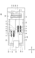
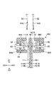
- FIG. 1 is a top view showing the semiconductor device according to the first embodiment.
- FIG. 2 is a front view showing the semiconductor device according to the first embodiment;
- FIG. 3 is a top view showing the relationship between the P terminal and N terminal and the circuit pattern in the semiconductor device according to the first embodiment.
- FIG. 4 is a cross-sectional view showing the relationship between the P terminal and N terminal and the circuit pattern in the semiconductor device according to the first embodiment.
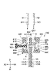
- FIG. 5 is a cross-sectional view (part 1) showing the terminal fixture in the semiconductor device according to the first embodiment.
- FIG. 6 is a cross-sectional view (part 2) showing the terminal fixture in the semiconductor device according to the first embodiment.
- FIG. 7 is a circuit diagram showing the semiconductor device according to the first embodiment.
- FIG. 8 is a cross-sectional view showing a terminal fixture to which first external terminals and second external terminals are fixed in the first embodiment.
- FIG. 9 is a cross-sectional view showing the semiconductor device according to the second embodiment.
- FIG. 10 is a cross-sectional view showing the semiconductor device according to the second embodiment.
- FIG. 11 is a cross-sectional view showing a semiconductor device according to the third embodiment.
- FIG. 12 is a top view showing the semiconductor device according to the fourth embodiment.
- FIG. 13 is a cross-sectional view (part 1) showing a terminal fixture for an O terminal in a semiconductor device according to a fourth embodiment;
- FIG. 14 is a cross-sectional view (part 2) showing the terminal fixture for the O terminal in the semiconductor device according to the fourth embodiment.
- FIG. 15 is a cross-sectional view showing a terminal fixture in a semiconductor device according to the fifth embodiment.
- FIG. 16 is a cross-sectional view showing a terminal fixture to which first external terminals and second external terminals are fixed in the fifth embodiment.
- FIG. 17 is a cross-sectional view showing a terminal fixture in a semiconductor device according to the sixth embodiment.
- FIG. 18 is a cross-sectional view showing a terminal fixture to which first external terminals and second external terminals are fixed in the sixth embodiment.
- FIG. 19 is a cross-sectional view showing a terminal fixture in a semiconductor device according to the seventh embodiment.
- FIG. 20 is a cross-sectional view showing a terminal fixture to which first external terminals and second external terminals are fixed in the seventh embodiment.
- FIG. 21 is a cross-sectional view showing a terminal fixture in a semiconductor device according to the eighth embodiment.
- FIG. 22 is a cross-sectional view showing a terminal fixture to which first external terminals and second external terminals are fixed in
- An object of the present disclosure is to provide a semiconductor device capable of reducing inductance in internal terminals.
- the inductance at the internal terminals can be reduced.
- a semiconductor device has a first main surface and a second main surface opposite to the first main surface, and has a first internal terminal to which a first external terminal is connected. a second internal terminal having a terminal, a third main surface, and a fourth main surface opposite to the third main surface, to which the second external terminal is connected; a semiconductor element connected between two internal terminals; a first pressing member pressing the first external terminal against the second principal surface; and a second pressing member pressing the second external terminal against the fourth principal surface. and a member, wherein the first main surface and the third main surface are parallel, and at least a portion of the first main surface and at least a portion of the third main surface face each other.
- the first main surface and the third main surface are parallel, and at least part of the first main surface and at least part of the third main surface face each other. Therefore, the current flowing through the flat plate portion of the first internal terminal and the current flowing through the flat plate portion of the second internal terminal flow in directions opposite to each other. The magnetic field around the flat plate portion of the internal terminal cancels each other out. Therefore, the difference in inductance between the P terminal and the N terminal is almost eliminated, and the inductance at the internal terminals can be reduced.
- the second main surface and the fourth main surface may be parallel to each other.
- the first external terminals and the second external terminals can be pressed from opposite directions, the first external terminals can be easily pressed against the second main surface and the second external terminals can be easily pressed against the fourth main surface.
- a circuit pattern provided with the semiconductor element is provided, and the first principal surface, the second principal surface, the third principal surface and the fourth principal surface are the It may be perpendicular to the circuit pattern. In this case, it is easy to bring the first external terminal and the second external terminal into contact with the first internal terminal and the second internal terminal from a direction perpendicular to the circuit pattern.
- a circuit pattern provided with the semiconductor element is provided, and the first principal surface, the second principal surface, the third principal surface and the fourth principal surface are the It may be parallel to the circuit pattern. In this case, it is easy to bring the first external terminal and the second external terminal into contact with the first internal terminal and the second internal terminal from a direction parallel to the circuit pattern.
- the first pressing member has a first bolt that presses the first external terminal against the second principal surface
- the second pressing member has the fourth
- a second bolt for pressing the second external terminal may be provided on the main surface. In this case, by tightening the first bolt and the second bolt, the first external terminal can be pressed against the second principal surface and the second external terminal can be pressed against the fourth principal surface.
- the first pressing member has a first cushioning member sandwiched between the first bolt and the first external terminal, and the second pressing member includes the second bolt and the second external terminal.
- the pressure applied from the first bolt to the first external terminal is dispersed by the first cushioning member
- the pressure applied from the second bolt to the second external terminal is dispersed by the second cushioning member.
- the first cushioning member has a first detent on the surface facing the second main surface
- the second cushioning member has a surface facing the fourth main surface. It may have a second detent.
- the adhesion strength between the first cushioning member and the second main surface and the adhesion strength between the second cushioning member and the fourth main surface can be improved.
- the first internal terminal has a first concave portion on the second main surface
- the second internal terminal has a second concave portion on the fourth main surface
- the first cushioning member may have a first projection that fits into the first recess
- the second cushioning member may have a second projection that fits into the second recess.
- the first protrusion fits into the first recess and the second protrusion fits into the second recess, whereby the first external terminal and the second external terminal are separated from the first internal terminal and the second internal terminal, respectively. It can be done easily.
- an insulating member is provided between the first internal terminal and the second internal terminal, and the first bolt penetrates the first internal terminal.
- a through hole may be formed, and a hole into which the first bolt passing through the through hole is fitted may be formed in the insulating member.
- the first bolt penetrates the through hole and fits into the hole of the insulating member, thereby making it difficult for the first external terminal to come off from the first internal terminal.
- a first through hole is formed in the first internal terminal
- a second through hole is formed in the second internal terminal
- the first pressing member A through hole and a bolt passing through the second through hole may be provided, and the second pressing member may have a nut fitted to the bolt.
- the bolt passes through the first through hole and the second through hole, and the nut is fitted to the bolt, so that the first external terminal and the second external terminal are not easily separated from the first internal terminal and the second internal terminal, respectively. can.
- the first pressing member may have a first leaf spring
- the second pressing member may have a second leaf spring.
- the first external terminal and the second external terminal can be connected to the semiconductor device by simple work.
- a third internal terminal having a fifth main surface and a sixth main surface opposite to the fifth main surface, to which a third external terminal is connected; and a third pressing member that presses the third external terminal on the sixth main surface, and the plurality of semiconductor elements are connected in series between the first internal terminal and the second internal terminal.
- the third internal terminal may be connected between two semiconductor elements of the plurality of semiconductor elements.
- the configuration around the third internal terminal becomes similar to the configuration around the first internal terminal and the second internal terminal, which facilitates the work of connecting the third external terminal to the third internal terminal.
- the semiconductor element may contain silicon, silicon carbide, or gallium nitride.
- a power module or the like can be configured by using a semiconductor element containing silicon, silicon carbide, or gallium nitride.
- a plane including the X1-X2 direction and the Y1-Y2 direction is the XY plane
- a plane including the Y1-Y2 direction and the Z1-Z2 direction is the YZ plane
- a plane including the Z1-Z2 direction and the X1-X2 direction is the ZX plane.
- the Z1 direction is defined as the upward direction
- the Z2 direction is defined as the downward direction.
- planar viewing means viewing an object from the Z1 side.
- FIG. 1 is a top view showing the semiconductor device according to the first embodiment.
- FIG. 2 is a front view showing the semiconductor device according to the first embodiment;
- FIG. 1 is a top view showing the semiconductor device according to the first embodiment.
- a semiconductor device 100 mainly has a P terminal 110, an N terminal 120, an O terminal 130, a base plate 140, a case 150, and a terminal fixture 160.
- the P terminal 110 is a positive power supply terminal
- the N terminal 120 is a negative power supply terminal
- the O terminal 130 is an output terminal.
- P terminal 110 , N terminal 120 , and O terminal 130 are attached to case 150 .
- the P terminal 110 is an example of a first internal terminal
- the N terminal 120 is an example of a second internal terminal
- the O terminal is an example of a third internal terminal.
- the X1-X2 direction is the direction along the long sides of the rectangular base plate 140 and the case 150 in plan view
- the Y1-Y2 direction is the direction along the short sides of the base plate 140 and the case 150
- the Z1-Z2 direction is the direction along the normal to the base plate 140 and the case 150 .
- the base plate 140 is, for example, a plate-like body that is rectangular in plan view and has a uniform thickness.
- the base plate 140 has a major surface 141 .
- the material of the base plate 140 is a metal having high thermal conductivity, such as copper (Cu), copper alloy, aluminum (Al), or the like.
- the base plate 140 is fixed to a cooler or the like using a thermal interface material (TIM) or the like.
- the case 150 is, for example, frame-shaped in plan view.
- the material of the case 150 is an insulator such as resin.
- the case 150 has a pair of side wall portions 151 and 152 facing each other, and a pair of end wall portions 153 and 154 connecting both ends of the side wall portions 151 and 152 .
- the side wall portions 151 and 152 are arranged parallel to the ZX plane, and the end wall portions 153 and 154 are arranged parallel to the YZ plane.
- the side wall portion 152 is arranged on the Y2 side of the side wall portion 151
- the end wall portion 154 is arranged on the X2 side of the end wall portion 153 .
- An insulating substrate 170 is arranged on the Z1 side of the base plate 140 . That is, the insulating substrate 170 is arranged on the main surface 141 of the base plate 140 .
- the insulating substrate 170 has a first circuit pattern 171, a second circuit pattern 172 and a third circuit pattern 173 on the Z1 side surface, and a conductive layer 179 on the Z2 side surface (see FIGS. 4 and 6).
- the first circuit pattern 171, the second circuit pattern 172 and the third circuit pattern 173 are parallel to the XY plane.
- a conductive layer 179 is bonded to the base plate 140 with a bonding material such as solder.
- a plurality of first transistors 11 and a plurality of first diodes 21 are mounted on the first circuit pattern 171 .
- a plurality of second transistors 12 and a plurality of second diodes 22 are mounted on the second circuit pattern 172 .
- the first transistor 11, the first diode 21, the second transistor 12 and the second diode 22 are examples of semiconductor elements.
- the first transistor 11 has a first gate electrode, a first source electrode and a first drain electrode.
- the first gate electrode and the first source electrode are arranged on the main surface of the first transistor 11 on the Z1 side, and the first drain electrode is arranged on the main surface on the Z2 side of the first transistor 11 .
- the first drain electrode is bonded to the first circuit pattern 171 with a bonding material such as solder.
- the first diode 21 has a first anode electrode and a first cathode electrode.
- the first anode electrode is arranged on the main surface of the first diode 21 on the Z1 side, and the first cathode electrode is arranged on the main surface on the Z2 side of the first diode 21 .
- the first cathode electrode is joined to the first circuit pattern 171 with a joining material such as solder.
- the second transistor 12 has a second gate electrode, a second source electrode and a second drain electrode.
- the second gate electrode and the second source electrode are arranged on the main surface of the second transistor 12 on the Z1 side, and the second drain electrode is arranged on the main surface on the Z2 side of the second transistor 12 .
- a second drain electrode is joined to the second circuit pattern 172 by a joining material such as solder.
- the second diode 22 has a second anode electrode and a second cathode electrode.
- the second anode electrode is arranged on the main surface of the second diode 22 on the Z1 side, and the second cathode electrode is arranged on the main surface on the Z2 side of the second diode 22 .
- a second cathode electrode is joined to the second circuit pattern 172 with a joining material such as solder.
- the semiconductor device 100 has multiple wires 31 , multiple wires 32 , multiple wires 41 , and multiple wires 42 .
- a wire 31 connects the first source electrode of the first transistor 11 and the second circuit pattern 172 .
- a wire 32 connects the first source electrode of the first transistor 11 and the first anode electrode of the first diode 21 .
- a wire 41 connects the second source electrode of the second transistor 12 and the third circuit pattern 173 .
- a wire 42 connects the second source electrode of the second transistor 12 and the second anode electrode of the second diode 22 .
- the semiconductor device 100 includes gate terminals, auxiliary source terminals, gate wires, auxiliary source wires, circuit patterns connecting the gate wires, circuit patterns connecting the auxiliary source wires, etc., but descriptions thereof will be omitted for convenience.
- illustration of the gate electrode is omitted in FIG. 1 and the like.
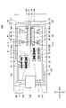
- FIG. 3 is a top view showing the relationship between the P terminal 110 and the N terminal 120 and the first circuit pattern 171 and the third circuit pattern 173 in the semiconductor device according to the first embodiment.
- FIG. 4 is a cross-sectional view showing the relationship between the P terminal 110 and N terminal 120 and the first circuit pattern 171 and third circuit pattern 173 in the semiconductor device according to the first embodiment.
- FIG. 4 corresponds to a cross-sectional view taken along line IV-IV in FIG. 3 and 4, the case 150 is omitted.
- the P terminal 110 has a flat plate portion 111 and a contact portion 112 .
- the flat plate portion 111 has a first principal surface 111A and a second principal surface 111B opposite to the first principal surface 111A.
- the first main surface 111A and the second main surface 111B are surfaces parallel to the YZ plane and perpendicular to the X1-X2 direction.
- the first main surface 111A and the second main surface 111B are surfaces perpendicular to the first circuit pattern 171, the second circuit pattern 172, and the third circuit pattern 173, respectively.
- the first main surface 111A is on the X1 side of the second main surface 111B.
- the flat plate portion 111 is separated from the first circuit pattern 171 and the third circuit pattern 173 on the Z1 side.
- the contact portion 112 extends from the Z2 side end of the flat plate portion 111 and is bent toward the X2 side.
- the contact portion 112 is connected to the first circuit pattern 171 via a bonding material such
- the N terminal 120 has a flat plate portion 121 and a contact portion 122 .
- the flat plate portion 121 has a third principal surface 121A and a fourth principal surface 121B opposite to the third principal surface 121A.
- the third main surface 121A and the fourth main surface 121B are surfaces parallel to the YZ plane and perpendicular to the X1-X2 direction.
- the third main surface 121A and the fourth main surface 121B are surfaces perpendicular to the first circuit pattern 171, the second circuit pattern 172, and the third circuit pattern 173, respectively.
- the third main surface 121A is on the X2 side of the fourth main surface 121B.
- the flat plate portion 121 is separated from the first circuit pattern 171 and the third circuit pattern 173 on the Z1 side.
- the contact portion 122 extends from the Z2 side end portion of the flat plate portion 121 and is bent toward the X2 side.
- the contact portion 122 is connected to the third circuit pattern 173 via a bonding material
- the flat plate portion 111 of the P terminal 110 is on the X2 side of the flat plate portion 121 of the N terminal 120 .
- 111 A of 1st main surfaces and 121 A of 3rd main surfaces are parallel, and 111 A of 1st main surfaces and 121 A of 3rd main surfaces mutually oppose.
- the flat plate portion 111 and the flat plate portion 121 overlap each other on the Z1 side of the insulating substrate 170 when viewed from the X1-X2 direction.
- the distance between the first major surface 111A and the third major surface 121A is preferably 5 mm or less, more preferably 3 mm or less.
- the O terminal 130 is connected to the second circuit pattern 172 via a bonding material such as solder.
- the O terminal 130 extends to the X2 side of the case 150 through the Z1 side of the end wall portion 154, for example.
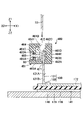
- FIG. 5 and 6 are cross-sectional views showing the terminal fixture 160 in the semiconductor device according to the first embodiment.
- FIG. 5 corresponds to a cross-sectional view taken along line V-V in FIG.
- FIG. 6 corresponds to a cross-sectional view taken along line VI-VI in FIG.
- the case 150 is omitted.
- the terminal fixture 160 mainly has a housing 61 , a partition wall 62 , a first bolt 63 , a first pressing terminal 64 , a second bolt 65 and a second pressing terminal 66 .
- the housing 61 is fixed to the case 150, for example.
- the housing 61 is in contact with, for example, the side wall portion 151 , the side wall portion 152 and the end wall portion 153 and is separated from the end wall portion 154 .
- the housing 61 has a rectangular parallelepiped external shape including a lower wall portion 61A, an upper wall portion 61B, a side wall portion 61C, a side wall portion 61D, a side wall portion 61E, and a side wall portion 61F.
- the lower wall portion 61A and upper wall portion 61B are parallel to the XY plane
- the side wall portions 61C and 61D are parallel to the YZ plane
- the side wall portions 61E and 61F are parallel to the ZX plane.
- the upper wall portion 61B is located on the Z1 side of the lower wall portion 61A.
- the side wall portion 61C is located on the X2 side of the side wall portion 61D.
- the side wall portion 61E is on the Y2 side of the side wall portion 61F.
- An opening 71 is formed in the center of the lower wall portion 61A in the X1-X2 direction.
- a flat plate portion 111 of the P terminal 110 and a flat plate portion 121 of the N terminal 120 extend through the opening 71 into the housing 61 .
- Partition wall 62 is provided between flat plate portion 111 and flat plate portion 121 .
- the partition wall 62 is connected to the side wall portion 61E and the side wall portion 61F.
- a metal plate 62A is provided on the surface of the partition wall 62 facing the upper end of the flat plate portion 111, and a metal plate 62B is provided on the surface of the partition wall 62 facing the upper end of the flat plate portion 121. As shown in FIG.
- the metal plate 62A and the metal plate 62B are made of metal having high buckling strength such as steel.
- a surface 62C of the metal plate 62A facing the first main surface 111A of the flat plate portion 111 may be subjected to anti-rotation processing such as knurling.
- a surface 62D of the metal plate 62B facing the third main surface 121A of the flat plate portion 121 may be subjected to anti-rotation processing such as knurling.
- An opening 72 is formed in the center of the upper wall portion 61B in the X1-X2 direction.
- a first external terminal 51 connected to the P terminal 110 and a second external terminal 52 connected to the N terminal 120 are inserted into the housing 61 through the opening 72 .
- the shape of the first external terminal 51 and the second external terminal 52 is, for example, a plate shape.
- a first bolt hole 81A is formed in the side wall portion 61C, and a first female screw 82A is provided in the first bolt hole 81A.
- the first female screw 82A is made of a metal having high buckling strength such as steel.
- the first bolt 63 is fitted into the first female thread 82A so that the head of the first bolt 63 is located on the X2 side of the side wall portion 61C.
- a tip surface 63X of the first bolt 63 faces the second main surface 111B of the flat plate portion 111. As shown in FIG.
- the metal plate 62A is provided so as to overlap the tip surface 63X of the first bolt 63 when viewed from the X1-X2 direction.
- the first bolt 63 is, for example, a hexagon socket bolt.
- a first pressing terminal 64 is arranged between the tip surface 63X of the first bolt 63 and the second main surface 111B of the flat plate portion 111 .
- the first pressing terminal 64 is provided so as to be movable in the X1-X2 direction as the first bolt 63 is tightened and loosened.
- the first pressing terminal 64 is sandwiched between the first bolt 63 and the first external terminal 51 when the first external terminal 51 is inserted into the housing 61 .
- the first pressing terminal 64 is made of a metal having high buckling strength, such as steel.
- the first pressing terminal 64 is made of, for example, a metal plate.
- the surface 64X of the first pressing terminal 64 facing the second main surface 111B of the flat plate portion 111 may be subjected to anti-rotation processing such as knurling.
- the first pressing terminal 64 may have a first detent 91 on the surface 64X.
- the first pressing terminal 64 is provided at the end on the Z1 side so as to guide the tip of the first external terminal 51 between the tip end surface 63X of the first bolt 63 and the second main surface 111B of the flat plate portion 111 . You may have the inclined surface 64Y inclined from the main surface 111B.
- the first pressing terminal 64 is an example of a first cushioning member.
- a first pressing member 67 includes a first bolt 63 and a first pressing terminal 64 .
- a plurality of sets, for example two sets, of the first bolt 63, the first bolt hole 81A and the first female screw 82A may be provided.
- a plurality of first pressing terminals 64 may be provided so as to correspond to each of the plurality of sets, or only one may be provided in common to the plurality of sets.
- a second bolt hole 81B is formed in the side wall portion 61D, and a second female screw 82B is provided in the second bolt hole 81B.
- the second female screw 82B is made of a metal having high buckling strength such as steel.
- the second bolt 65 is fitted into the second female thread 82B so that the head of the second bolt 65 is positioned on the X1 side of the side wall portion 61D.
- a tip surface 65X of the second bolt 65 faces the fourth main surface 121B of the flat plate portion 121.
- the metal plate 62B is provided so as to overlap the tip surface 65X of the second bolt 65 when viewed from the X1-X2 direction.
- the second bolt 65 is, for example, a hexagon socket bolt.
- An opening (not shown) for tightening and loosening the second bolt 65 is formed in the end wall portion 153 .
- a second pressing terminal 66 is arranged between the tip end surface 65X of the second bolt 65 and the fourth main surface 121B of the flat plate portion 121 .
- the second pressing terminal 66 is provided so as to be movable in the X1-X2 direction as the second bolt 65 is tightened and loosened.
- the second pressing terminal 66 is sandwiched between the second bolt 65 and the second external terminal 52 when the second external terminal 52 is inserted into the housing 61 .
- the second pressing terminal 66 is made of metal such as steel having high buckling strength.
- the second pressing terminal 66 is made of, for example, a metal plate.
- the surface 66X of the second pressing terminal 66 facing the fourth main surface 121B of the flat plate portion 121 may be subjected to anti-rotation processing such as knurling.
- the second push terminal 66 may have a second detent 92 on the surface 66X.
- the second pressing terminal 66 is provided at the end on the Z1 side so as to guide the tip of the second external terminal 52 between the tip surface 65X of the second bolt 65 and the fourth main surface 121B of the flat plate portion 121. You may have the inclined surface 66Y inclined from the main surface 121B.
- the second pressing terminal 66 is an example of a second cushioning member.
- a second bolt 65 and a second pressing terminal 66 are included in the second pressing member 68 .
- a plurality of sets, for example two sets, of the second bolt 65, the second bolt hole 81B and the second female screw 82B may be provided.
- a plurality of second pressing terminals 66 may be provided so as to correspond to each of the plurality of sets, or only one second pressing terminal 66 may be provided in common to the plurality of sets.
- the housing 61 and the partition wall 62 are made of resin such as polyphenylene sulfide (PPS), and may be resin molded products.
- the metal plate 62A and the metal plate 62B may be insert-molded in the partition wall 62 .
- FIG. 7 is a circuit diagram showing the semiconductor device according to the first embodiment.
- the first drain electrode of the first transistor 11 and the first cathode electrode of the first diode 21 are connected to the P terminal 110 via the first circuit pattern 171 .
- the source electrode of the first transistor 11 is connected to the O terminal 130 via the second circuit pattern 172 and the wire 31 , and the first anode electrode of the first diode 21 is connected via the wire 32 .
- the first drain electrode of the first transistor 11 and the first cathode electrode of the first diode 21 are commonly connected to the P terminal 110, and the first source electrode of the first transistor 11 and the first cathode electrode of the first diode 21 are connected in common.
- 1 anode electrode is commonly connected to the O terminal 130 . That is, the first transistor 11 and the first diode 21 are connected in parallel between the P terminal 110 and the O terminal 130 .
- a second drain electrode of the second transistor 12 and a second cathode electrode of the second diode 22 are connected to the O terminal 130 via the second circuit pattern 172 .
- the source electrode of the second transistor 12 is connected to the N terminal 120 via the third circuit pattern 173 and the wire 41
- the second anode electrode of the second diode 22 is connected via the wire 42 .
- the second drain electrode of the second transistor 12 and the second cathode electrode of the second diode 22 are commonly connected to the O terminal 130
- the second source electrode of the second transistor 12 and the second cathode electrode of the second diode 22 are connected in common.
- 2 anode electrodes are commonly connected to the N terminal 120 . That is, the second transistor 12 and the second diode 22 are connected in parallel between the O terminal 130 and the N terminal 120 .
- the upper arm 1 includes a first transistor 11 and a first diode 21.
- Lower arm 2 includes second transistor 12 and second diode 22 .
- Upper arm 1 and lower arm 2 are connected in series between P terminal 110 and N terminal 120 .
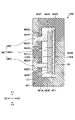
- FIG. 8 is a cross-sectional view showing the terminal fixture 160 to which the first external terminal 51 and the second external terminal 52 are fixed in the first embodiment.
- the first bolt 63 is loosened, and a gap between the surface 64X of the first pressing terminal 64 and the second main surface 111B is secured. , form a gap larger than the thickness of the first external terminal 51 .
- the second bolt 65 is loosened to form a gap larger than the thickness of the second external terminal 52 between the surface 66X of the second pressing terminal 66 and the fourth main surface 121B.
- the first bolt 63 is inserted between the surface 64X of the first pressing terminal 64 and the second main surface 111B of the flat plate portion 111 while the first external terminal 51 is aligned along the inclined surface 64Y of the first pressing terminal 64. is inserted up to the Z2 side of the tip end surface 63X.
- the second bolt 65 is inserted between the surface 66X of the second pressing terminal 66 and the fourth main surface 121B of the flat plate portion 121 while the second external terminal 52 is aligned along the inclined surface 66Y of the second pressing terminal 66. is inserted up to the Z2 side of the tip end surface 65X.
- the first external terminal 51 is pressed against the flat plate portion 111 via the first pressing terminal 64 .
- the second external terminal 52 is pressed against the flat plate portion 121 via the second pressing terminal 66 .
- the first external terminal 51 is fixed to the P terminal 110
- the second external terminal 52 is fixed to the N terminal 120
- the first external terminal 51 and the second external terminal 52 can be connected to the semiconductor device 100.
- the current flowing through the flat plate portion 111 of the P terminal 110 and the current flowing through the flat plate portion 121 of the N terminal 120 flow in opposite directions. Therefore, the magnetic field around the flat plate portion 111 and the magnetic field around the flat plate portion 121 cancel each other out. Therefore, according to the present embodiment, the magnetic fields cancel each other over a wide range of the P terminal 110 and the N terminal 120, and the inductance at the P terminal 110 and the N terminal 120 can be reduced.
- first main surface 111A, the second main surface 111B, the third main surface 121A and the fourth main surface 121B are perpendicular to the first circuit pattern 171 and the third circuit pattern 173, they are perpendicular to the main surface 141 of the base plate 140.
- the first external terminal 51 and the second external terminal 52 can be inserted into the terminal fixture 160 from any direction. Therefore, it is easy to bring the first external terminal 51 and the second external terminal 52 into contact with the P terminal 110 and the N terminal 120, respectively.
- the first pressing member 67 includes the first bolt 63 and the second pressing member 68 includes the second bolt 65
- the second main surface 111B is provided with the first external force.
- the terminal 51 can be firmly pressed, and the second external terminal 52 can be firmly pressed against the fourth main surface 121B.
- the second main surface 111B and the fourth main surface 121B are parallel to each other, the first external terminal 51 and the second external terminal 52 can be pressed from opposite directions. Therefore, the first external terminal 51 can be easily pressed against the second main surface 111B, and the second external terminal 52 can be easily pressed against the fourth main surface 121B.
- the first pressing terminal 64 is sandwiched between the first bolt 63 and the first external terminal 51
- the second pressing terminal 66 is sandwiched between the second bolt 65 and the second external terminal 52 . Therefore, the pressure applied from the first bolt 63 to the first external terminal 51 is dispersed by the first pressing terminal 64
- the pressure applied from the second bolt 65 to the second external terminal 52 is dispersed by the second pressing terminal 66 .
- the current tends to concentrate in areas where the contact pressure is strong, but by dispersing the pressure by the first pressing terminals 64 and the second pressing terminals 66, the concentration of the current can be alleviated and the heat generated due to the concentration of the current can be suppressed.
- the adhesion strength between the first pressing terminal 64 and the second main surface 111B can be improved.
- the adhesion strength between the second pressing terminal 66 and the fourth main surface 121B can be improved.
- FIG. 9 is a cross-sectional view showing the semiconductor device according to the second embodiment.
- FIG. 10 is a cross-sectional view showing the semiconductor device according to the second embodiment.
- FIG. 9 corresponds to a cross-sectional view at a position in the Z1-Z2 direction similar to FIG.
- FIG. 10 corresponds to a cross-sectional view taken along line XX in FIG.
- the housing 61, the partition wall 62, the metal plate 62A and the metal plate 62B are omitted.
- the case 150 is omitted.
- the first main surface 111A and the second main surface 111B of the P terminal 110 are surfaces parallel to the ZX plane and perpendicular to the Y1-Y2 direction.
- the first main surface 111A and the second main surface 111B are surfaces perpendicular to the first circuit pattern 171, the second circuit pattern 172, and the third circuit pattern 173, respectively.
- the first main surface 111A is on the Y2 side of the second main surface 111B.
- the flat plate portion 111 is separated from the first circuit pattern 171 on the Z1 side.
- the contact portion 112 extends from the Z2 side end portion of the flat plate portion 111 and is bent toward the Y1 side.
- the contact portion 112 is connected to the first circuit pattern 171 via a bonding material such as solder.
- the third main surface 121A and the fourth main surface 121B of the N terminal 120 are surfaces parallel to the ZX plane and perpendicular to the Y1-Y2 direction.
- the third main surface 121A and the fourth main surface 121B are surfaces perpendicular to the first circuit pattern 171, the second circuit pattern 172, and the third circuit pattern 173, respectively.
- the third main surface 121A is on the Y1 side of the fourth main surface 121B.
- the flat plate portion 121 is separated from the third circuit pattern 173 on the Z1 side.
- the contact portion 122 extends from the Z2 side end of the flat plate portion 121 and is bent toward the Y2 side.
- the contact portion 122 is connected to the third circuit pattern 173 via a bonding material such as solder.
- the flat plate portion 111 of the P terminal 110 is on the Y1 side of the flat plate portion 121 of the N terminal 120 .
- 111 A of 1st main surfaces and 121 A of 3rd main surfaces are parallel, and 111 A of 1st main surfaces and 121 A of 3rd main surfaces mutually oppose.
- the flat plate portion 111 and the flat plate portion 121 overlap each other on the Z1 side of the insulating substrate 170 when viewed from the Y1-Y2 direction.
- the flat plate portion 111 and the flat plate portion 121 are arranged in the X1-X2 direction, whereas in the second embodiment, the flat plate portion 111 and the flat plate portion 121 are arranged in the Y1-Y2 direction. I'm in. Along with this, the orientation of the terminal fixture 160 is rotated by 90° within the XY plane from that of the first embodiment.
- FIG. 11 is a cross-sectional view showing a semiconductor device according to the third embodiment.
- FIG. 11, like FIG. 5, corresponds to a cross-sectional view taken along line VV in FIG. In FIG. 10, the case 150 is omitted.
- a semiconductor device 300 according to the third embodiment has a P terminal 310 instead of the P terminal 110 and an N terminal 320 instead of the N terminal 120 .
- the P terminal 310 has a flat plate portion 311 , a contact portion 312 and a connecting portion 313 .
- the flat plate portion 311 has a first principal surface 311A and a second principal surface 311B opposite to the first principal surface 311A.
- the first main surface 311A and the second main surface 311B are surfaces parallel to the XY plane and perpendicular to the Z1-Z2 direction.
- the first main surface 311A and the second main surface 311B are surfaces parallel to the first circuit pattern 171 , the second circuit pattern 172 and the third circuit pattern 173 .
- the first main surface 311A is on the Z2 side of the second main surface 311B.
- the flat plate portion 311 is separated from the first circuit pattern 171 and the third circuit pattern 173 on the Z1 side.
- the contact portion 312 is connected to the first circuit pattern 171 via a bonding material such as solder.
- the connecting portion 313 extends from the X2 side end of the flat plate portion 311 to the Z2 side, and extends from the X1 side end of the contact portion 312 to the Z1 side.
- the connecting portion 313 connects the flat plate portion 311 and the contact portion 312 .
- the N terminal 320 has a flat plate portion 321 , a contact portion 322 and a connecting portion 323 .
- the flat plate portion 321 has a third principal surface 321A and a fourth principal surface 321B opposite to the third principal surface 321A.
- the third main surface 321A and the fourth main surface 321B are surfaces parallel to the XY plane and perpendicular to the Z1-Z2 direction.
- the third main surface 321A and the fourth main surface 321B are surfaces parallel to the first circuit pattern 171, the second circuit pattern 172 and the third circuit pattern 173. As shown in FIG.
- the third main surface 321A is on the Z1 side of the fourth main surface 321B.
- the flat plate portion 321 is separated from the first circuit pattern 171 and the third circuit pattern 173 on the Z1 side.
- the contact portion 322 is connected to the third circuit pattern 173 via a bonding material such as solder.
- the connecting portion 323 extends from the X2 side end of the flat plate portion 321 to the Z2 side, and extends from the X1 side end of the contact portion 322 to the Z1 side.
- the connecting portion 323 connects the flat plate portion 321 and the contact portion 322 .
- the flat plate portion 111 and the flat plate portion 121 are arranged in the X1-X2 direction, whereas in the third embodiment, the flat plate portion 111 and the flat plate portion 121 are arranged in the Z1-Z2 direction. I'm in. Along with this, the orientation of the terminal fixture 160 is rotated by 90° within the ZX plane from that of the first embodiment.
- the same effect as the first embodiment can be obtained by the third embodiment.
- the first principal surface 111A, the second principal surface 111B, the third principal surface 121A and the fourth principal surface 121B are parallel to the first circuit pattern 171 and the third circuit pattern 173, the principal surface 141 of the base plate 140
- the first external terminal 51 and the second external terminal 52 can be inserted into the terminal fixture 160 from a direction parallel to . Therefore, it is easy to bring the first external terminal 51 and the second external terminal 52 into contact with the P terminal 110 and the N terminal 120, respectively.
- FIG. 12 is a top view showing the semiconductor device according to the fourth embodiment.
- 13 and 14 are cross-sectional views showing a terminal fixture for an O terminal in a semiconductor device according to the fourth embodiment.
- FIG. 13 corresponds to a cross-sectional view taken along line VV in FIG.
- FIG. 14 corresponds to a cross-sectional view at a position in the Z1-Z2 direction similar to FIG. In FIG. 13, the case 150 is omitted.
- a semiconductor device 400 according to the fourth embodiment mainly has a P terminal 110, an N terminal 120, an O terminal 130, a base plate 140, a case 150, a terminal fixture 160, and a terminal fixture 460. .
- the O terminal 130 has a flat plate portion 131 and a contact portion 132 .
- the flat plate portion 131 has a fifth main surface 131A and a sixth main surface 131B opposite to the fifth main surface 131A.
- the fifth main surface 131A and the sixth main surface 131B are surfaces parallel to the YZ plane and perpendicular to the X1-X2 direction.
- the fifth main surface 131A and the sixth main surface 131B are surfaces perpendicular to the first circuit pattern 171, the second circuit pattern 172, and the third circuit pattern 173, respectively.
- the fifth main surface 131A is on the X1 side of the sixth main surface 131B.
- the flat plate portion 131 is separated from the second circuit pattern 172 on the Z1 side.
- the contact portion 132 extends from the Z2 side end of the flat plate portion 131 and is bent toward the X1 side.
- the contact portion 132 is connected to the second circuit pattern 172 via a bonding material such as solder.
- the terminal fixture 460 mainly has a housing 461 , a third bolt 463 and a third pressing terminal 464 .
- the housing 461 is fixed to the case 150, for example.
- the housing 461 is in contact with, for example, the side wall portion 151 , the side wall portion 152 , and the end wall portion 154 and is separated from the end wall portion 153 .
- the housing 461 has a rectangular parallelepiped external shape including a lower wall portion 461A, an upper wall portion 461B, a side wall portion 461C, a side wall portion 461D, a side wall portion 461E, and a side wall portion 461F.
- the lower wall portion 461A and the upper wall portion 461B are parallel to the XY plane, the side wall portions 461C and 461D are parallel to the YZ plane, and the side wall portions 461E and 461F are parallel to the ZX plane.
- the upper wall portion 461B is located on the Z1 side of the lower wall portion 461A.
- the side wall portion 461C is on the X2 side of the side wall portion 461D.
- the side wall portion 461E is on the Y2 side of the side wall portion 461F.
- An opening 471 is formed in the lower wall portion 461A.
- a flat plate portion 131 of the O terminal 130 extends to the inside of the housing 461 through the opening 471 .
- a metal plate 462A is provided on a surface of the side wall portion 461D that faces the upper end of the flat plate portion 131 .
- the metal plate 462A is made of a metal having high buckling strength such as steel.
- a surface 462C of the metal plate 462A facing the fifth main surface 131A of the flat plate portion 131 may be subjected to anti-rotation processing such as knurling.
- An opening 472 is formed in the upper wall portion 461B.
- a third external terminal 53 connected to the O terminal 130 is inserted into the housing 461 through the opening 472 .
- the shape of the third external terminal 53 is, for example, a plate shape.
- a third bolt hole 481A is formed in the side wall portion 461C, and a third female screw 482A is provided in the third bolt hole 481A.
- the third female screw 482A is made of a metal having high buckling strength such as steel.
- the third bolt 463 is fitted into the third female screw 482A so that the head of the third bolt 463 is positioned on the X2 side of the side wall portion 461C.
- a tip surface 463X of the third bolt 463 faces the sixth main surface 131B of the flat plate portion 131 .
- the metal plate 462A is provided so as to overlap the tip surface 463X of the third bolt 463 when viewed from the X1-X2 direction.
- the third bolt 463 is, for example, a hexagon socket bolt. An opening (not shown) for tightening and loosening the third bolt 463 is formed in the end wall portion 154 .
- a third pressing terminal 464 is arranged between the tip surface 463X of the third bolt 463 and the sixth main surface 131B of the flat plate portion 131 .
- the third pressing terminal 464 is provided so as to be movable in the X1-X2 direction as the third bolt 463 is tightened and loosened.
- the third pressing terminal 464 is sandwiched between the third bolt 463 and the third external terminal 53 when the third external terminal 53 is inserted into the housing 61 .
- the third pressing terminal 464 is made of metal such as steel having high buckling strength.
- the third pressing terminal 464 is made of, for example, a metal plate.
- a surface 464X of the third pressing terminal 464 facing the sixth main surface 131B of the flat plate portion 131 may be subjected to anti-rotation processing such as knurling.
- the third push terminal 464 may have a third detent 93 on the surface 464X.
- the third pressing terminal 464 is provided at the end on the Z1 side so as to guide the tip of the third external terminal 53 between the tip surface 463X of the third bolt 463 and the sixth main surface 131B of the flat plate portion 131 . It may have an inclined surface 464Y inclined from the main surface 131B.
- the third pressing terminal 464 is an example of a third cushioning member.
- a third bolt 463 and a third pressing terminal 464 are included in the third pressing member 467 .
- a plurality of sets, for example two sets, of the third bolt 463, the third bolt hole 481A and the third female screw 482A may be provided.
- a plurality of third pressing terminals 464 may be provided so as to correspond to each of the plurality of sets, or only one third pressing terminal 464 may be provided in common to the plurality of sets.
- the housing 461 is made of resin such as polyphenylene sulfide (PPS), and may be a resin molded product.
- the metal plate 462A may be insert-molded into the side wall portion 461D.
- the third bolt 463 is tightened between the surface 464X of the third pressing terminal 464 and the sixth main surface 131B of the flat plate portion 131. is pushed to the Z2 side of the tip surface 463X.
- the third external terminal 53 can be fixed to the O terminal 130 and connected to the semiconductor device 100 .
- the configuration around the O terminal 130 becomes similar to the configuration around the P terminal 110 and the N terminal 120, so that the work of connecting the third external terminal 53 to the O terminal 130 can be facilitated.
- FIG. 15 is a cross-sectional view showing a terminal fixture in a semiconductor device according to the fifth embodiment.
- the first pressing terminal 64 has a columnar first protrusion 64Z that protrudes from the surface 64X toward the X1 side.
- the second pressing terminal 66 has a columnar second protrusion 66Z that protrudes from the surface 66X toward the X2 side.
- the flat plate portion 111 is formed with a first concave portion 111X into which the first convex portion 64Z is fitted, and the first external terminal 51 is formed with a through hole 51X through which the first convex portion 64Z penetrates.
- the flat plate portion 131 is formed with a second concave portion 121X into which the second convex portion 66Z is fitted, and the second external terminal 52 is formed with a through hole 52X through which the second convex portion 66Z penetrates.
- the length of the first protrusion 64Z that is, the dimension in the X1-X2 direction is approximately the same as the sum of the thickness of the first external terminal 51 and the depth of the first recess 111X.
- the length of the second protrusion 66Z that is, the dimension in the X1-X2 direction is approximately the same as the sum of the thickness of the second external terminal 52 and the depth of the second recess 121X.
- the metal plate 62A and the metal plate 62B may not be provided on the partition wall 62.
- FIG. 16 is a cross-sectional view showing the terminal fixture 160 to which the first external terminals 51 and the second external terminals 52 are fixed in the fifth embodiment.
- the first bolt 63 is loosened, and the first protrusion 64Z of the first pressing terminal 64 and the second main surface 111B are aligned. A gap larger than the thickness of the first external terminal 51 is formed between them.
- the second bolt 65 is loosened to form a gap larger than the thickness of the second external terminal 52 between the second projection 66Z of the second pressing terminal 66 and the fourth main surface 121B.
- the first external terminal 51 is inserted between the first projection 64Z and the second main surface 111B of the flat plate portion 111 so that the through hole 51X is aligned with the first recess 111X in the X1-X2 direction.
- the second external terminal 52 is inserted between the second convex portion 66Z and the fourth main surface 121B of the flat plate portion 121 so that the through hole 52X is aligned with the second concave portion 121X in the X1-X2 direction.
- Alignment portions such as spacers may be provided in the housing 61 so that the through holes 51X are aligned with the first recesses 111X and the through holes 52X are aligned with the second recesses 121X in a self-aligning manner.
- the first protrusion 64Z is inserted into the through-hole 51X and fitted into the first recess 111X. Press to 111.
- the second protrusion 66Z is inserted into the through hole 52X, and while being fitted into the second recess 121X, the second external terminal 52 is attached to the flat plate portion via the second pressing terminal 66. Press 121.
- the first external terminal 51 is fixed to the P terminal 110
- the second external terminal 52 is fixed to the N terminal 120
- the first external terminal 51 and the second external terminal 52 can be connected to the semiconductor device 100.
- the same effect as the first embodiment can be obtained by the fifth embodiment. Further, since the movement of the first external terminal 51 and the second external terminal 52 in the Z1-Z2 direction is restrained, the first external terminal 51 and the second external terminal 52 are removed from the P terminal 110 and the N terminal 120, respectively. It can be done easily.
- first recess 111X may be a through hole penetrating the flat plate portion 111
- second recess 121X may be a through hole penetrating the flat plate portion 121.
- FIG. 17 is a cross-sectional view showing a terminal fixture in a semiconductor device according to the sixth embodiment.
- a through hole 61X having a size through which the head of the first bolt 63 can pass is formed in the side wall portion 61C instead of the first bolt hole 81A, and the first female screw 82A is provided.
- a through hole 64 ⁇ /b>A through which the shaft portion of the first bolt 63 passes is formed in the first pressing terminal 64 .
- a through hole 111Y through which the shaft portion of the first bolt 63 passes is formed in the flat plate portion 111, and a through hole 51Y through which the shaft portion of the first bolt 63 passes is formed in the first external terminal 51.
- a bolt hole 62X is formed in the partition wall 62, and a female screw 62Y is provided in the bolt hole 62X.
- the internal thread 32Y is made of a metal having high buckling strength such as steel.
- An insulating paper 69 is arranged between the bolt hole 62X and the female screw 62Y and the flat plate portion 121.
- the partition wall 62 is not provided with the metal plate 62A and the metal plate 62B.
- the partition wall 62 is an example of an insulating member
- the bolt hole 62X is an example of a hole into which a first bolt is fitted.
- FIG. 18 is a cross-sectional view showing the terminal fixture 160 to which the first external terminals 51 and the second external terminals 52 are fixed in the sixth embodiment.
- the first bolt 63 is removed from the female screw 62Y, and the surface 64X of the first pressing terminal 64 and the second pressing terminal 64 are separated from each other.
- a gap larger than the thickness of the first external terminal 51 is formed between the principal surface 111B.
- the second bolt 65 is loosened to form a gap larger than the thickness of the second external terminal 52 between the surface 66X of the second pressing terminal 66 and the fourth main surface 121B.
- the X1-X2 direction is inserted so that the through hole 51Y is aligned with the through hole 111Y.
- the second external terminal 52 is aligned with the inclined surface 66Y of the second pressing terminal 66
- the second bolt 65 is inserted between the surface 66X of the second pressing terminal 66 and the fourth main surface 121B of the flat plate portion 121. Insert up to the Z2 side of the tip surface 65X.
- a positioning portion such as a spacer may be provided in the housing 61 so that the through hole 51Y is aligned with the through hole 111Y in a self-aligning manner.
- the first bolt 63 is inserted into the through hole 64A, the through hole 51Y, and the through hole 111Y.
- the first external terminal 51 is pressed against the flat plate portion 111 .
- the second external terminal 52 is pressed against the flat plate portion 121 via the second pressing terminal 66 .
- the first external terminal 51 is fixed to the P terminal 110
- the second external terminal 52 is fixed to the N terminal 120
- the first external terminal 51 and the second external terminal 52 can be connected to the semiconductor device 100.
- the insulating paper 69 is provided, the first bolt 63 is electrically insulated from the N terminal 120 .
- an electrically insulating material such as resin or ceramic may be used as the material of the first bolt 63 while keeping the female screw 62Y from contacting the flat plate portion 121 .
- the insulating paper 69 may not be provided.
- the configuration on the P terminal 110 side and the configuration on the N terminal 120 side may be interchanged.
- the second external terminal 52 can be made difficult to come off from the N terminal 120 .
- FIG. 19 is a cross-sectional view showing a terminal fixture in a semiconductor device according to the seventh embodiment.
- a through hole 61X having a size through which the head of the first bolt 63 can pass is formed in the side wall portion 61C instead of the first bolt hole 81A, and the first female screw 82A is provided.
- a through hole 64A through which the shaft portion of the first bolt 63 passes is formed in the first pressing terminal 64.
- a through hole 111Y through which the shaft portion of the first bolt 63 passes is formed in the flat plate portion 111, and a through hole 51Y through which the shaft portion of the first bolt 63 passes is formed in the first external terminal 51.
- FIG. A through hole 62Z through which the shaft portion of the first bolt 63 passes is formed in the partition wall 62 .
- a through hole 121Y through which the shaft of the first bolt 63 passes is formed in the flat plate portion 121, and a through hole 52Y through which the shaft of the first bolt 63 passes is formed in the second external terminal 52.
- a through hole 66A through which the shaft portion of the first bolt 63 passes is formed in the second pressing terminal 66.
- the partition wall 62 is not provided with the metal plate 62A and the metal plate 62B.
- the through-hole 111Y is an example of a first through-hole
- the through-hole 121Y is an example of a second through-hole.
- a nut 75 into which the first bolt 63 is fitted is arranged on the X1 side of the second pressing terminal 66 .
- the side wall portion 61D is formed with a through hole 61Y having a size through which the nut 75 can pass, and the second female screw 82B is not provided.
- the nut 75 is an example of a second pressing member.
- the material of the first bolt 63 is an electrically insulating material such as resin or ceramic.
- the material of the nut 75 may be the same material as the material of the first bolt 63 .
- FIG. 20 is a cross-sectional view showing the terminal fixture 160 to which the first external terminals 51 and the second external terminals 52 are fixed in the seventh embodiment.
- the first bolt 63 is removed from the nut 75, and the surface 64X of the first pressing terminal 64 and the second A gap larger than the thickness of the first external terminal 51 is formed between the main surface 111B and a gap larger than the thickness of the second external terminal 52 between the surface 66X of the second pressing terminal 66 and the fourth main surface 121B. form a large gap.
- the X1-X2 direction is inserted so that the through hole 51Y is aligned with the through hole 111Y.
- the second external terminal 52 is aligned with the inclined surface 66Y of the second pressing terminal 66
- a contact is placed between the surface 66X of the second pressing terminal 66 and the fourth main surface 121B of the flat plate portion 121 in the X1-X2 direction.
- the through hole 52Y is inserted so as to line up with the through hole 121Y.
- Alignment portions such as spacers may be provided in the housing 61 so that the through holes 51Y are aligned with the through holes 111Y and the through holes 52Y are aligned with the through holes 121Y in a self-aligning manner.
- the first bolt 63 is inserted into the through hole 64A, the through hole 51Y, the through hole 111Y, the through hole 62Z, the through hole 121Y, and the through hole 66A, and the first bolt 63 and the nut 75 are screwed together.
- the first external terminal 51 is pressed against the flat plate portion 111 via the first pressing terminal 64
- the second external terminal 52 is pressed against the flat plate portion 121 via the second pressing terminal 66 .
- the first external terminal 51 is fixed to the P terminal 110
- the second external terminal 52 is fixed to the N terminal 120
- the first external terminal 51 and the second external terminal 52 can be connected to the semiconductor device 100.
- the seventh embodiment also provides the same effects as the first embodiment. Further, since the movement of the first external terminal 51 and the second external terminal 52 in the Z1-Z2 direction is restrained, the first external terminal 51 and the second external terminal 52 are removed from the P terminal 110 and the N terminal 120, respectively. It can be done easily.
- FIG. 21 is a cross-sectional view showing a terminal fixture in a semiconductor device according to the eighth embodiment.
- openings 871 and 873 are formed in the lower wall portion 61A instead of the opening 71.
- Flat plate portion 111 of P terminal 110 extends into housing 61 through opening 871
- flat plate portion 121 of N terminal 120 extends into housing 61 through opening 873 .
- An opening 872 and an opening 874 are formed instead of the opening 72 in the upper wall portion 61B. In the Z1-Z2 direction, the openings 871 and 872 overlap, and the openings 873 and 874 overlap.
- the partition wall 62 is not provided with the metal plate 62A and the metal plate 62B. Also, the first bolt 63, the first pressing terminal 64, the first bolt hole 81A, the first female screw 82A, the second bolt 65, the second pressing terminal 66, the second bolt hole 81B and the second female screw 82B are not provided. .
- a leaf spring 801, a leaf spring 802, a leaf spring 803, and a leaf spring 804 are arranged between the partition wall 62 and the side wall portion 61C.
- Leaf springs 801 and 802 extend from the lower wall portion 61A toward the Z1 side.
- the leaf springs 803 and 804 extend from the upper wall portion 61B to the Z2 side.
- the leaf springs 801 and 803 are arranged closer to the partition wall 62 than the openings 871 and 872, contact the first main surface 111A of the flat plate portion 111, and bias the flat plate portion 111 toward the X2 side.
- the leaf springs 802 and 804 are arranged closer to the side wall portion 61C than the openings 871 and 872, and the distance between the leaf springs 802 and 804 and the second main surface 111B of the flat plate portion 111 in a natural state is It is smaller than the thickness of the first external terminal 51 .
- Leaf springs 801 to 804 are examples of first leaf springs.
- a leaf spring 805, a leaf spring 806, a leaf spring 807, and a leaf spring 808 are arranged between the partition wall 62 and the side wall portion 61D.
- Leaf springs 805 and 806 extend from the lower wall portion 61A to the Z1 side.
- Leaf springs 807 and 808 extend from the upper wall portion 61B toward the Z2 side.
- the plate springs 805 and 807 are arranged closer to the partition wall 62 than the openings 873 and 874, contact the third main surface 121A of the flat plate portion 121, and bias the flat plate portion 121 toward the X1 side.
- the leaf springs 806 and 807 are arranged closer to the side wall portion 61D than the openings 873 and 874, and in a natural state, the distance between the leaf springs 806 and 808 and the fourth main surface 121B of the flat plate portion 121 is It is smaller than the thickness of the second external terminal 52 .
- Leaf springs 805 to 808 are examples of second leaf springs.
- FIG. 22 is a cross-sectional view showing the terminal fixture 160 to which the first external terminals 51 and the second external terminals 52 are fixed in the eighth embodiment.
- the first external terminal 51 is connected to the leaf springs 804 and 802 and the second main surface 111B of the flat plate portion 111 through the opening 872. insert between Similarly, the second external terminal 52 is inserted through the opening 874 between the plate spring 804 and between the plate spring 802 and the fourth main surface 121B of the flat plate portion 121 .
- the plate spring 804 and the plate spring 802 are deformed toward the X2 side and bias the first external terminal 51 toward the X1 side. That is, leaf springs 801 to 804 press first external terminal 51 against flat plate portion 111 .
- the leaf springs 808 and 806 are deformed toward the X1 side and bias the second external terminal 52 toward the X2 side. That is, leaf springs 805 to 808 press second external terminal 52 against flat plate portion 121 .
- the first external terminal 51 is fixed to the P terminal 110
- the second external terminal 52 is fixed to the N terminal 120
- the first external terminal 51 and the second external terminal 52 can be connected to the semiconductor device 100.
- the first external terminal 51 and the second external terminal 52 can be connected to the semiconductor device 100 by a simple operation.
- semiconductor elements include, for example, silicon, silicon carbide, or gallium nitride.
- a power module or the like can be configured by using a semiconductor element containing silicon, silicon carbide, or gallium nitride.
- semiconductor devices containing silicon carbide are suitable for high withstand voltage power modules.
Abstract
半導体装置は、第1主面と、前記第1主面とは反対側の第2主面とを有し、第1外部端子が接続される第1内部端子と、第3主面と、前記第3主面とは反対側の第4主面とを有し、第2外部端子が接続される第2内部端子と、前記第1内部端子及び前記第2内部端子の間に接続された半導体素子と、前記第2主面に前記第1外部端子を押圧する第1押圧部材と、前記第4主面に前記第2外部端子を押圧する第2押圧部材と、を有し、前記第1主面と前記第3主面とが平行であり、前記第1主面の少なくとも一部と、前記第3主面の少なくとも一部とが互いに対向する。
Description
本開示は、半導体装置に関する。
本出願は、2021年4月1日出願の日本出願第2021-062726号に基づく優先権を主張し、前記日本出願に記載された全ての記載内容を援用するものである。
内部配線のインダクタンスの低減を目的とした半導体装置が提案されている(特許文献1)。
本開示の半導体装置は、第1主面と、前記第1主面とは反対側の第2主面とを有し、第1外部端子が接続される第1内部端子と、第3主面と、前記第3主面とは反対側の第4主面とを有し、第2外部端子が接続される第2内部端子と、前記第1内部端子及び前記第2内部端子の間に接続された半導体素子と、前記第2主面に前記第1外部端子を押圧する第1押圧部材と、前記第4主面に前記第2外部端子を押圧する第2押圧部材と、を有し、前記第1主面と前記第3主面とが平行であり、前記第1主面の少なくとも一部と、前記第3主面の少なくとも一部とが互いに対向する。
[本開示が解決しようとする課題]
従来の半導体装置によっても、内部端子におけるインダクタンスを十分に低減することは困難である。
従来の半導体装置によっても、内部端子におけるインダクタンスを十分に低減することは困難である。
本開示は、内部端子におけるインダクタンスを低減できる半導体装置を提供することを目的とする。
[本開示の効果]
本開示によれば、内部端子におけるインダクタンスを低減できる。
本開示によれば、内部端子におけるインダクタンスを低減できる。
実施するための形態について、以下に説明する。
[本開示の実施形態の説明]
最初に本開示の実施態様を列記して説明する。以下の説明では、同一または対応する要素には同一の符号を付し、それらについて同じ説明は繰り返さない。
最初に本開示の実施態様を列記して説明する。以下の説明では、同一または対応する要素には同一の符号を付し、それらについて同じ説明は繰り返さない。
〔1〕 本開示の一態様に係る半導体装置は、第1主面と、前記第1主面とは反対側の第2主面とを有し、第1外部端子が接続される第1内部端子と、第3主面と、前記第3主面とは反対側の第4主面とを有し、第2外部端子が接続される第2内部端子と、前記第1内部端子及び前記第2内部端子の間に接続された半導体素子と、前記第2主面に前記第1外部端子を押圧する第1押圧部材と、前記第4主面に前記第2外部端子を押圧する第2押圧部材と、を有し、前記第1主面と前記第3主面とが平行であり、前記第1主面の少なくとも一部と、前記第3主面の少なくとも一部とが互いに対向する。
第1主面と第3主面とが平行であり、第1主面の少なくとも一部と、第3主面の少なくとも一部とが互いに対向している。このため、第1内部端子の平板部を流れる電流と、第2内部端子の平板部を流れる電流とは、互いに逆方向に流れることとなり、第1内部端子の平板部の周囲の磁界と第2内部端子の平板部の周囲の磁界とが互いに相殺される。従って、P端子とN端子との間のインダクタンスの差がほとんどなくなり、内部端子におけるインダクタンスを低減できる。
〔2〕 〔1〕において、前記第2主面と前記第4主面とが互いに平行であってもよい。この場合、互いに逆方向から第1外部端子及び第2外部端子を押圧できるため、第2主面に第1外部端子を押圧しやすく、第4主面に第2外部端子を押圧しやすくできる。
〔3〕 〔1〕又は〔2〕において、前記半導体素子が設けられた回路パターンを有し、前記第1主面、前記第2主面、前記第3主面及び前記第4主面が前記回路パターンに垂直であってもよい。この場合、第1外部端子及び第2外部端子を回路パターンに垂直な方向から第1内部端子及び第2内部端子に接触させやすい。
〔4〕 〔1〕又は〔2〕において、前記半導体素子が設けられた回路パターンを有し、前記第1主面、前記第2主面、前記第3主面及び前記第4主面が前記回路パターンに平行であってもよい。この場合、第1外部端子及び第2外部端子を回路パターンに平行な方向から第1内部端子及び第2内部端子に接触させやすい。
〔5〕 〔1〕~〔4〕において、前記第1押圧部材は、前記第2主面に前記第1外部端子を押圧する第1ボルトを有し、前記第2押圧部材は、前記第4主面に前記第2外部端子を押圧する第2ボルトを有してもよい。この場合、第1ボルト及び第2ボルトを締めることで、第2主面に第1外部端子を押圧し、第4主面に第2外部端子を押圧できる。
〔6〕 〔5〕において、前記第1押圧部材は、前記第1ボルトと前記第1外部端子との間に挟まれる第1緩衝部材を有し、前記第2押圧部材は、前記第2ボルトと前記第2外部端子との間に挟まれる第2緩衝部材を有してもよい。この場合、第1ボルトから第1外部端子にかかる圧力が第1緩衝部材により分散され、第2ボルトから第2外部端子にかかる圧力が第2緩衝部材により分散される。このため、圧力の集中に伴う電流の集中が緩和され、電流の集中に伴う発熱を抑制できる。
〔7〕 〔6〕において、前記第1緩衝部材は、前記第2主面に対向する面に第1回り止めを有し、前記第2緩衝部材は、前記第4主面に対向する面に第2回り止めを有してもよい。この場合、第1緩衝部材と第2主面との間の密着強度及び第2緩衝部材と第4主面との間の密着強度を向上できる。
〔8〕 〔6〕又は〔7〕において、前記第1内部端子が前記第2主面に第1凹部を有し、前記第2内部端子が前記第4主面に第2凹部を有し、前記第1緩衝部材が前記第1凹部に嵌る第1凸部を有し、前記第2緩衝部材が前記第2凹部に嵌る第2凸部を有してもよい。この場合、第1凸部が第1凹部に嵌り、第2凸部が第2凹部に嵌ることで、第1外部端子及び第2外部端子を、それぞれ第1内部端子及び第2内部端子から外れにくくできる。
〔9〕 〔5〕~〔8〕において、前記第1内部端子と前記第2内部端子との間に設けられた絶縁部材を有し、前記第1内部端子に、前記第1ボルトが貫通する貫通孔が形成され、前記絶縁部材に、前記貫通孔を貫通した前記第1ボルトが嵌る孔が形成されていてもよい。この場合、第1ボルトが貫通孔を貫通して絶縁部材の孔に嵌ることで、第1外部端子を第1内部端子から外れにくくできる。
〔10〕 〔1〕~〔4〕において、前記第1内部端子に第1貫通孔が形成され、前記第2内部端子に第2貫通孔が形成され、前記第1押圧部材は、前記第1貫通孔及び前記第2貫通孔を貫通するボルトを有し、前記第2押圧部材は、前記ボルトに嵌るナットを有してもよい。この場合、ボルトが第1貫通孔及び第2貫通孔を貫通し、ナットがボルトに嵌ることで、第1外部端子及び第2外部端子を、それぞれ第1内部端子及び第2内部端子から外れにくくできる。
〔11〕 〔1〕~〔4〕において、前記第1押圧部材は、第1板ばねを有し、前記第2押圧部材は、第2板ばねを有してもよい。この場合、簡易な作業によって第1外部端子及び第2外部端子を半導体装置に接続できる。
〔12〕 〔1〕~〔11〕において、第5主面と、前記第5主面とは反対側の第6主面とを有し、第3外部端子が接続される第3内部端子と、前記第6主面に第3外部端子を押圧する第3押圧部材と、を有し、前記第1内部端子と前記第2内部端子との間に、複数の前記半導体素子が直列に接続され、前記第3内部端子は、複数の前記半導体素子のうちの2つの半導体素子の間に接続されてもよい。この場合、第3内部端子の周囲の構成が第1内部端子及び第2内部端子の周囲の構成と同様になり、第3外部端子を第3内部端子に接続する作業を行いやすくできる。
〔13〕 〔1〕~〔12〕において、前記半導体素子は、シリコン、炭化珪素又は窒化ガリウムを含んでもよい。シリコン、炭化珪素又は窒化ガリウムを含む半導体素子を用いることでパワーモジュール等を構成できる。
[本開示の実施形態の詳細]
以下、本開示の実施形態について詳細に説明するが、本実施形態はこれらに限定されるものではない。なお、本明細書及び図面において、実質的に同一の機能構成を有する構成要素については、同一の符号を付することにより重複した説明を省くことがある。本明細書及び図面において、X1-X2方向、Y1-Y2方向、Z1-Z2方向を相互に直交する方向とする。X1-X2方向及びY1-Y2方向を含む面をXY面とし、Y1-Y2方向及びZ1-Z2方向を含む面をYZ面とし、Z1-Z2方向及びX1-X2方向を含む面をZX面とする。便宜上、Z1方向を上方向、Z2方向を下方向とする。また、本開示において平面視とは、Z1側から対象物を視ることをいう。
以下、本開示の実施形態について詳細に説明するが、本実施形態はこれらに限定されるものではない。なお、本明細書及び図面において、実質的に同一の機能構成を有する構成要素については、同一の符号を付することにより重複した説明を省くことがある。本明細書及び図面において、X1-X2方向、Y1-Y2方向、Z1-Z2方向を相互に直交する方向とする。X1-X2方向及びY1-Y2方向を含む面をXY面とし、Y1-Y2方向及びZ1-Z2方向を含む面をYZ面とし、Z1-Z2方向及びX1-X2方向を含む面をZX面とする。便宜上、Z1方向を上方向、Z2方向を下方向とする。また、本開示において平面視とは、Z1側から対象物を視ることをいう。
(第1実施形態)
まず、第1実施形態について説明する。図1は、第1実施形態に係る半導体装置を示す上面図である。図2は、第1実施形態に係る半導体装置を示す正面図である。
まず、第1実施形態について説明する。図1は、第1実施形態に係る半導体装置を示す上面図である。図2は、第1実施形態に係る半導体装置を示す正面図である。
第1実施形態に係る半導体装置100は、主として、P端子110と、N端子120と、O端子130と、ベース板140と、ケース150と、端子固定具160とを有する。P端子110は正極側の電源端子であり、N端子120は負極側の電源端子であり、O端子130は出力端子である。P端子110、N端子120、O端子130はケース150に組み付けられている。P端子110は第1内部端子の一例であり、N端子120は第2内部端子の一例であり、O端子は第3内部端子の一例である。X1-X2方向は平面視で矩形状のベース板140及びケース150の長辺に沿う方向であり、Y1-Y2方向はベース板140及びケース150の短辺に沿う方向であり、Z1-Z2方向はベース板140及びケース150の法線に沿う方向である。
ベース板140は、例えば平面視で矩形状の厚さが一様の板状体である。ベース板140は、主面141を備える。ベース板140の材料は、熱伝導率の高い素材である金属、例えば銅(Cu)、銅合金、アルミニウム(Al)等である。ベース板140は、熱界面材料(thermal interface material:TIM)等を用いて冷却器等に固定される。
ケース150は、例えば平面視において枠状に形成されている。ケース150の材料は樹脂等の絶縁体である。ケース150は、互いに対向する一対の側壁部151及び側壁部152と、側壁部151及び側壁部152の両端をつなぐ一対の端壁部153及び端壁部154とを有する。側壁部151及び側壁部152はZX平面に平行に配置され、端壁部153及び端壁部154はYZ平面に平行に配置されている。側壁部152は側壁部151のY2側に配置され、端壁部154は端壁部153のX2側に配置されている。
ベース板140のZ1側に、絶縁基板170が配置されている。つまり、ベース板140の主面141に絶縁基板170が配置されている。絶縁基板170は、Z1側の面に第1回路パターン171、第2回路パターン172及び第3回路パターン173を有し、Z2側の面に導電層179を有する(図4及び図6参照)。第1回路パターン171、第2回路パターン172及び第3回路パターン173は、XY平面に平行である。導電層179が、はんだ等の接合材によりベース板140に接合されている。
第1回路パターン171の上に複数の第1トランジスタ11及び複数の第1ダイオード21が実装されている。第2回路パターン172の上に複数の第2トランジスタ12及び複数の第2ダイオード22が実装されている。第1トランジスタ11、第1ダイオード21、第2トランジスタ12及び第2ダイオード22は半導体素子の一例である。
第1トランジスタ11は、第1ゲート電極と、第1ソース電極と、第1ドレイン電極とを有する。第1ゲート電極及び第1ソース電極は第1トランジスタ11のZ1側の主面に配置され、第1ドレイン電極は第1トランジスタ11のZ2側の主面に配置されている。第1ドレイン電極がはんだ等の接合材により第1回路パターン171に接合されている。
第1ダイオード21は、第1アノード電極と、第1カソード電極とを有する。第1アノード電極は第1ダイオード21のZ1側の主面に配置され、第1カソード電極は第1ダイオード21のZ2側の主面に配置されている。第1カソード電極がはんだ等の接合材により第1回路パターン171に接合されている。
第2トランジスタ12は、第2ゲート電極と、第2ソース電極と、第2ドレイン電極とを有する。第2ゲート電極及び第2ソース電極は第2トランジスタ12のZ1側の主面に配置され、第2ドレイン電極は第2トランジスタ12のZ2側の主面に配置されている。第2ドレイン電極がはんだ等の接合材により第2回路パターン172に接合されている。
第2ダイオード22は、第2アノード電極と、第2カソード電極とを有する。第2アノード電極は第2ダイオード22のZ1側の主面に配置され、第2カソード電極は第2ダイオード22のZ2側の主面に配置されている。第2カソード電極がはんだ等の接合材により第2回路パターン172に接合されている。
半導体装置100は、複数のワイヤ31と、複数のワイヤ32と、複数のワイヤ41と、複数のワイヤ42とを有する。ワイヤ31は、第1トランジスタ11の第1ソース電極と第2回路パターン172とを接続する。ワイヤ32は、第1トランジスタ11の第1ソース電極と第1ダイオード21の第1アノード電極とを接続する。ワイヤ41は、第2トランジスタ12の第2ソース電極と第3回路パターン173とを接続する。ワイヤ42は、第2トランジスタ12の第2ソース電極と第2ダイオード22の第2アノード電極とを接続する。
なお、半導体装置100は、ゲート端子、補助ソース端子、ゲートワイヤ、補助ソースワイヤ、ゲートワイヤを繋ぐ回路パターン、補助ソースワイヤを繋ぐ回路パターン等も含むが、便宜上、それらについての説明を省略する。また、図1等では、ゲート電極の図示を省略している。
ここで、P端子110及びN端子120について詳細に説明する。図3は、第1実施形態に係る半導体装置におけるP端子110及びN端子120と第1回路パターン171及び第3回路パターン173との関係を示す上面図である。図4は、第1実施形態に係る半導体装置におけるP端子110及びN端子120と第1回路パターン171及び第3回路パターン173との関係を示す断面図である。図4は、図3中のIV-IV線に沿った断面図に相当する。図3及び図4では、ケース150を省略している。
P端子110は、平板部111と、コンタクト部112とを有する。平板部111は、第1主面111Aと、第1主面111Aとは反対側の第2主面111Bとを有する。第1主面111A及び第2主面111Bは、YZ平面に平行、かつX1-X2方向に垂直な面である。第1主面111A及び第2主面111Bは、第1回路パターン171、第2回路パターン172及び第3回路パターン173に垂直な面である。第1主面111Aが第2主面111BのX1側にある。平板部111は、第1回路パターン171及び第3回路パターン173からZ1側に離れている。コンタクト部112は、平板部111のZ2側の端部から延び、X2側に屈曲されている。コンタクト部112は、はんだ等の接合材を介して第1回路パターン171に接続されている。
N端子120は、平板部121と、コンタクト部122とを有する。平板部121は、第3主面121Aと、第3主面121Aとは反対側の第4主面121Bとを有する。第3主面121A及び第4主面121Bは、YZ平面に平行、かつX1-X2方向に垂直な面である。第3主面121A及び第4主面121Bは、第1回路パターン171、第2回路パターン172及び第3回路パターン173に垂直な面である。第3主面121Aが第4主面121BのX2側にある。平板部121は、第1回路パターン171及び第3回路パターン173からZ1側に離れている。コンタクト部122は、平板部121のZ2側の端部から延び、X2側に屈曲されている。コンタクト部122は、はんだ等の接合材を介して第3回路パターン173に接続されている。
P端子110の平板部111はN端子120の平板部121のX2側にある。第1主面111Aと第3主面121Aとが平行であり、第1主面111Aと第3主面121Aとが互いに対向する。X1-X2方向から見たときに、絶縁基板170のZ1側において、平板部111と平板部121とが重なり合っている。第1主面111Aと第3主面121Aとの間の距離は、好ましくは5mm以下であり、より好ましくは3mm以下である。
O端子130は、はんだ等の接合材を介して第2回路パターン172に接続されている。O端子130は、例えば端壁部154のZ1側を通じてケース150のX2側に延びる。
ここで、端子固定具160について詳細に説明する。図5及び図6は、第1実施形態に係る半導体装置における端子固定具160を示す断面図である。図5は、図1中のV-V線に沿った断面図に相当する。図6は、図2中のVI-VI線に沿った断面図に相当する。図5では、ケース150を省略している。
端子固定具160は、主として、筐体61と、隔壁62と、第1ボルト63と、第1押圧端子64と、第2ボルト65と、第2押圧端子66とを有する。
筐体61は、例えばケース150に固定されている。筐体61は、例えば側壁部151と、側壁部152と、端壁部153とに接し、端壁部154から離れている。筐体61は、下壁部61Aと、上壁部61Bと、側壁部61Cと、側壁部61Dと、側壁部61Eと、側壁部61Fとを備えた直方体状の外形を有する。下壁部61A及び上壁部61BはXY平面に平行であり、側壁部61C及び側壁部61DはYZ平面に平行であり、側壁部61E及び側壁部61FはZX平面に平行である。上壁部61Bは下壁部61AのZ1側にある。側壁部61Cは側壁部61DのX2側にある。側壁部61Eは側壁部61FのY2側にある。
下壁部61AのX1-X2方向の中央に開口71が形成されている。P端子110の平板部111及びN端子120の平板部121が開口71を通じて筐体61の内部まで延びている。隔壁62は、平板部111と平板部121との間に設けられている。隔壁62は側壁部61E及び側壁部61Fに連結されている。隔壁62の平板部111の上端に対向する面に金属板62Aが設けられ、隔壁62の平板部121の上端に対向する面に金属板62Bが設けられている。金属板62A及び金属板62Bは、例えば鉄鋼等の座屈強度が高い金属製である。金属板62Aの平板部111の第1主面111Aに対向する面62Cにローレット加工等の回り止め加工が施されていてもよい。金属板62Bの平板部121の第3主面121Aに対向する面62Dにローレット加工等の回り止め加工が施されていてもよい。
上壁部61BのX1-X2方向の中央に開口72が形成されている。開口72を通じて、P端子110に接続される第1外部端子51と、N端子120に接続される第2外部端子52とが筐体61内に挿入される。第1外部端子51及び第2外部端子52の形状は、例えば板状である。Z2側から筐体61を見たときに、平板部111の第2主面111Bと開口72のX2側の縁との間の距離は第1外部端子51の厚さより大きく、平板部121の第4主面121Bと開口72のX1側の縁との間の距離は第2外部端子52の厚さより大きい。
側壁部61Cに、第1ボルト孔81Aが形成され、第1ボルト孔81A内に第1雌ねじ82Aが設けられている。第1雌ねじ82Aは、例えば鉄鋼等の座屈強度が高い金属製である。第1ボルト63は、第1ボルト63の頭部が側壁部61CのX2側に位置するようにして第1雌ねじ82Aに嵌まっている。第1ボルト63の先端面63Xが平板部111の第2主面111Bに対向する。金属板62Aは、X1-X2方向から見たときに、第1ボルト63の先端面63Xと重なるように設けられている。第1ボルト63は、例えば六角穴付きボルトである。
第1ボルト63の先端面63Xと平板部111の第2主面111Bとの間に第1押圧端子64が配置されている。第1押圧端子64は、第1ボルト63の締め及び緩めに付随してX1-X2方向に移動可能に設けられている。第1押圧端子64は、第1外部端子51が筐体61内に挿入された時に、第1ボルト63と第1外部端子51との間に挟まれる。第1押圧端子64は、例えば鉄鋼等の座屈強度が高い金属製である。第1押圧端子64は、例えば、金属板から構成される。第1押圧端子64の平板部111の第2主面111Bに対向する面64Xに、ローレット加工等の回り止め加工が施されていてもよい。例えば、第1押圧端子64は面64Xに第1回り止め91を有してもよい。第1押圧端子64は、第1ボルト63の先端面63Xと平板部111の第2主面111Bとの間に第1外部端子51の先端を案内するように、Z1側の端部に第2主面111Bから傾斜した傾斜面64Yを有してもよい。第1押圧端子64は第1緩衝部材の一例である。第1ボルト63及び第1押圧端子64が第1押圧部材67に含まれる。
第1ボルト63、第1ボルト孔81A及び第1雌ねじ82Aの組は複数組、例えば2組設けられていてもよい。第1押圧端子64は、これら複数組のそれぞれに対応するように複数個設けられていてもよく、これら複数組に対して共通に1個のみ設けられていてもよい。
側壁部61Dに、第2ボルト孔81Bが形成され、第2ボルト孔81B内に第2雌ねじ82Bが設けられている。第2雌ねじ82Bは、例えば鉄鋼等の座屈強度が高い金属製である。第2ボルト65は、第2ボルト65の頭部が側壁部61DのX1側に位置するようにして第2雌ねじ82Bに嵌まっている。第2ボルト65の先端面65Xが平板部121の第4主面121Bに対向する。金属板62Bは、X1-X2方向から見たときに、第2ボルト65の先端面65Xと重なるように設けられている。第2ボルト65は、例えば六角穴付きボルトである。端壁部153に、第2ボルト65の締め及び緩めを行うための開口(図示せず)が形成されている。
第2ボルト65の先端面65Xと平板部121の第4主面121Bとの間に第2押圧端子66が配置されている。第2押圧端子66は、第2ボルト65の締め及び緩めに付随してX1-X2方向に移動可能に設けられている。第2押圧端子66は、第2外部端子52が筐体61内に挿入された時に、第2ボルト65と第2外部端子52との間に挟まれる。第2押圧端子66は、例えば鉄鋼等の座屈強度が高い金属製である。第2押圧端子66は、例えば、金属板から構成される。第2押圧端子66の平板部121の第4主面121Bに対向する面66Xに、ローレット加工等の回り止め加工が施されていてもよい。例えば、第2押圧端子66は面66Xに第2回り止め92を有してもよい。第2押圧端子66は、第2ボルト65の先端面65Xと平板部121の第4主面121Bとの間に第2外部端子52の先端を案内するように、Z1側の端部に第4主面121Bから傾斜した傾斜面66Yを有してもよい。第2押圧端子66は第2緩衝部材の一例である。第2ボルト65及び第2押圧端子66が第2押圧部材68に含まれる。
第2ボルト65、第2ボルト孔81B及び第2雌ねじ82Bの組は複数組、例えば2組設けられていてもよい。第2押圧端子66は、これら複数組のそれぞれに対応するように複数個設けられていてもよく、これら複数組に対して共通に1個のみ設けられていてもよい。
筐体61及び隔壁62は、例えばポリフェニレンサルファイド(PPS)等の樹脂から構成され、樹脂成型品であってもよい。金属板62A及び金属板62Bは隔壁62にインサート成形されていてもよい。
次に、第1実施形態に係る半導体装置100の回路構成について説明する。図7は、第1実施形態に係る半導体装置を示す回路図である。
P端子110に、第1回路パターン171を介して第1トランジスタ11の第1ドレイン電極及び第1ダイオード21の第1カソード電極が接続される。O端子130に、第2回路パターン172と、ワイヤ31とを介して第1トランジスタ11のソース電極が接続され、更にワイヤ32を介して第1ダイオード21の第1アノード電極が接続される。このように、第1トランジスタ11の第1ドレイン電極と第1ダイオード21の第1カソード電極とがP端子110に共通に接続され、第1トランジスタ11の第1ソース電極と第1ダイオード21の第1アノード電極とがO端子130に共通に接続される。つまり、第1トランジスタ11及び第1ダイオード21はP端子110とO端子130との間に並列に接続される。
O端子130に、第2回路パターン172を介して第2トランジスタ12の第2ドレイン電極及び第2ダイオード22の第2カソード電極が接続される。N端子120に、第3回路パターン173と、ワイヤ41とを介して第2トランジスタ12のソース電極が接続され、更にワイヤ42を介して第2ダイオード22の第2アノード電極が接続される。このように、第2トランジスタ12の第2ドレイン電極と第2ダイオード22の第2カソード電極とがO端子130に共通に接続され、第2トランジスタ12の第2ソース電極と第2ダイオード22の第2アノード電極とがN端子120に共通に接続される。つまり、第2トランジスタ12及び第2ダイオード22はO端子130とN端子120との間に並列に接続される。
上アーム1は、第1トランジスタ11と、第1ダイオード21とを含む。下アーム2は、第2トランジスタ12と、第2ダイオード22とを含む。P端子110とN端子120との間に上アーム1と下アーム2とが直列に接続されている。
ここで、第1外部端子51及び第2外部端子52を端子固定具160に固定する方法について説明する。図8は、第1実施形態において第1外部端子51及び第2外部端子52が固定された端子固定具160を示す断面図である。
第1外部端子51及び第2外部端子52を端子固定具160に固定する際には、まず、第1ボルト63を緩め、第1押圧端子64の面64Xと第2主面111Bとの間に、第1外部端子51の厚さよりも大きい隙間を形成する。同様に、第2ボルト65を緩め、第2押圧端子66の面66Xと第4主面121Bとの間に、第2外部端子52の厚さよりも大きい隙間を形成する。
次に、第1外部端子51を第1押圧端子64の傾斜面64Yに沿わせながら、第1押圧端子64の面64Xと平板部111の第2主面111Bとの間に、第1ボルト63の先端面63XよりもZ2側まで挿入する。同様に、第2外部端子52を第2押圧端子66の傾斜面66Yに沿わせながら、第2押圧端子66の面66Xと平板部121の第4主面121Bとの間に、第2ボルト65の先端面65XよりもZ2側まで挿入する。
次に、第1ボルト63を締めることで、第1押圧端子64を介して第1外部端子51を平板部111に押圧する。同様に、第2ボルト65を締めることで、第2押圧端子66を介して第2外部端子52を平板部121に押圧する。
このようにして、第1外部端子51をP端子110に固定し、第2外部端子52をN端子120に固定し、第1外部端子51及び第2外部端子52を半導体装置100に接続できる。
ここで、半導体装置100の動作について説明する。
半導体装置100では、上アーム1の第1トランジスタ11がターンオフに転じると、電流は下アーム2の第2ダイオード22に転流し、電流が減少する。また、下アーム2の第2トランジスタ12がターンオフに転じると、電流は上アーム1の第1ダイオード21に転流し、電流が減少する。そのため、P端子110からN端子120に至り、P端子110とN端子120との間に接続されたコンデンサ(図示せず)へと戻る経路における単位時間当たりの電流の変化(di/dt)は大きなものとなる。P端子110からN端子120に至る経路のインダクタンスが大きい場合、ΔV=L・di/dtで表されるサージ電圧が大きくなる。ここで、ΔVはサージ電圧、Lはインダクタンス、iは電流、tは時間である。
本実施形態では、P端子110の平板部111を流れる電流と、N端子120の平板部121を流れる電流との間では、流れる方向が逆方向である。このため、平板部111の周囲の磁界と平板部121の周囲の磁界とが互いに相殺される。従って、本実施形態によれば、P端子110及びN端子120の広範囲にわたって、磁界が打ち消し合い、P端子110及びN端子120におけるインダクタンスを低減できる。
第1主面111A、第2主面111B、第3主面121A及び第4主面121Bが第1回路パターン171及び第3回路パターン173に垂直であるため、ベース板140の主面141に垂直な方向から第1外部端子51及び第2外部端子52を端子固定具160に挿入できる。このため、第1外部端子51及び第2外部端子52を、それぞれP端子110及びN端子120に接触させやすい。
第1押圧部材67が第1ボルト63を含み、第2押圧部材68が第2ボルト65を含むため、第1ボルト63及び第2ボルト65を締めることで、第2主面111Bに第1外部端子51を強固に押圧し、第4主面121Bに第2外部端子52を強固に押圧できる。また、第2主面111Bと第4主面121Bとが互いに平行であるため、互いに逆方向から第1外部端子51及び第2外部端子52を押圧できる。このため、第2主面111Bに第1外部端子51を押圧しやすく、第4主面121Bに第2外部端子52を押圧しやすくできる。
第1押圧端子64が第1ボルト63と第1外部端子51との間に挟まれ、第2押圧端子66が第2ボルト65と第2外部端子52との間に挟まれる。このため、第1ボルト63から第1外部端子51にかかる圧力が第1押圧端子64により分散され、第2ボルト65から第2外部端子52にかかる圧力が第2押圧端子66により分散される。電流は、接触圧力が強い領域に集中しやすいが、第1押圧端子64及び第2押圧端子66による圧力の分散により電流の集中を緩和し、電流の集中に伴う発熱を抑制できる。
第1押圧端子64の面64Xにローレット加工等の回り止め加工が施されていると、第1押圧端子64と第2主面111Bとの間の密着強度を向上できる。同様に、第2押圧端子66の面66Xにローレット加工等の回り止め加工が施されていると、第2押圧端子66と第4主面121Bとの間の密着強度を向上できる。
(第2実施形態)
次に、第2実施形態について説明する。図9は、第2実施形態に係る半導体装置を示す断面図である。図10は、第2実施形態に係る半導体装置を示す断面図である。図9は、図6と同様のZ1-Z2方向の位置での断面図に相当する。図10は、図9中のX-X線に沿った断面図に相当する。図9では、筐体61、隔壁62、金属板62A及び金属板62Bを省略している。図10では、ケース150を省略している。
次に、第2実施形態について説明する。図9は、第2実施形態に係る半導体装置を示す断面図である。図10は、第2実施形態に係る半導体装置を示す断面図である。図9は、図6と同様のZ1-Z2方向の位置での断面図に相当する。図10は、図9中のX-X線に沿った断面図に相当する。図9では、筐体61、隔壁62、金属板62A及び金属板62Bを省略している。図10では、ケース150を省略している。
第2実施形態に係る半導体装置200では、P端子110の第1主面111A及び第2主面111Bは、ZX平面に平行、かつY1-Y2方向に垂直な面である。第1主面111A及び第2主面111Bは、第1回路パターン171、第2回路パターン172及び第3回路パターン173に垂直な面である。第1主面111Aが第2主面111BのY2側にある。平板部111は、第1回路パターン171からZ1側に離れている。コンタクト部112は、平板部111のZ2側の端部から延び、Y1側に屈曲されている。コンタクト部112は、はんだ等の接合材を介して第1回路パターン171に接続されている。
また、N端子120の第3主面121A及び第4主面121Bは、ZX平面に平行、かつY1-Y2方向に垂直な面である。第3主面121A及び第4主面121Bは、第1回路パターン171、第2回路パターン172及び第3回路パターン173に垂直な面である。第3主面121Aが第4主面121BのY1側にある。平板部121は、第3回路パターン173からZ1側に離れている。コンタクト部122は、平板部121のZ2側の端部から延び、Y2側に屈曲されている。コンタクト部122は、はんだ等の接合材を介して第3回路パターン173に接続されている。
P端子110の平板部111はN端子120の平板部121のY1側にある。第1主面111Aと第3主面121Aとが平行であり、第1主面111Aと第3主面121Aとが互いに対向する。Y1-Y2方向から見たときに、絶縁基板170のZ1側において、平板部111と平板部121とが重なり合っている。
このように、第1実施形態では、平板部111及び平板部121がX1-X2方向に並んでいるのに対し、第2実施形態では、平板部111及び平板部121がY1-Y2方向に並んでいる。また、これに伴って、端子固定具160の向きが第1実施形態からXY平面内で90°回転した向きとなっている。
他の構成は第1実施形態と同様である。
第2実施形態によっても第1実施形態と同様の効果が得られる。
(第3実施形態)
次に、第3実施形態について説明する。図11は、第3実施形態に係る半導体装置を示す断面図である。図11は、図5と同様に、図1中のV-V線に沿った断面図に相当する。図10では、ケース150を省略している。
次に、第3実施形態について説明する。図11は、第3実施形態に係る半導体装置を示す断面図である。図11は、図5と同様に、図1中のV-V線に沿った断面図に相当する。図10では、ケース150を省略している。
第3実施形態に係る半導体装置300は、P端子110に代えてP端子310を有し、N端子120に代えてN端子320を有する。
P端子310は、平板部311と、コンタクト部312と、連結部313とを有する。平板部311は、第1主面311Aと、第1主面311Aとは反対側の第2主面311Bとを有する。第1主面311A及び第2主面311Bは、XY平面に平行、かつZ1-Z2方向に垂直な面である。第1主面311A及び第2主面311Bは、第1回路パターン171、第2回路パターン172及び第3回路パターン173に平行な面である。第1主面311Aが第2主面311BのZ2側にある。平板部311は、第1回路パターン171及び第3回路パターン173からZ1側に離れている。コンタクト部312は、はんだ等の接合材を介して第1回路パターン171に接続されている。連結部313は、平板部311のX2側の端部からZ2側に延び、かつコンタクト部312のX1側の端部からZ1側に延びる。連結部313は、平板部311とコンタクト部312とを連結する。
N端子320は、平板部321と、コンタクト部322と、連結部323とを有する。平板部321は、第3主面321Aと、第3主面321Aとは反対側の第4主面321Bとを有する。第3主面321A及び第4主面321Bは、XY平面に平行、かつZ1-Z2方向に垂直な面である。第3主面321A及び第4主面321Bは、第1回路パターン171、第2回路パターン172及び第3回路パターン173に平行な面である。第3主面321Aが第4主面321BのZ1側にある。平板部321は、第1回路パターン171及び第3回路パターン173からZ1側に離れている。コンタクト部322は、はんだ等の接合材を介して第3回路パターン173に接続されている。連結部323は、平板部321のX2側の端部からZ2側に延び、かつコンタクト部322のX1側の端部からZ1側に延びる。連結部323は、平板部321とコンタクト部322とを連結する。
このように、第1実施形態では、平板部111及び平板部121がX1-X2方向に並んでいるのに対し、第3実施形態では、平板部111及び平板部121がZ1-Z2方向に並んでいる。また、これに伴って、端子固定具160の向きが第1実施形態からZX平面内で90°回転した向きとなっている。
他の構成は第1実施形態と同様である。
第3実施形態によっても第1実施形態と同様の効果が得られる。また、第1主面111A、第2主面111B、第3主面121A及び第4主面121Bが第1回路パターン171及び第3回路パターン173に平行であるため、ベース板140の主面141に平行な方向から第1外部端子51及び第2外部端子52を端子固定具160に挿入できる。このため、第1外部端子51及び第2外部端子52を、それぞれP端子110及びN端子120に接触させやすい。
(第4実施形態)
次に、第4実施形態について説明する。図12は、第4実施形態に係る半導体装置を示す上面図である。図13及び図14は、第4実施形態に係る半導体装置におけるO端子用の端子固定具を示す断面図である。図13は、図12中のV-V線に沿った断面図に相当する。図14は、図6と同様のZ1-Z2方向の位置での断面図に相当する。図13では、ケース150を省略している。
次に、第4実施形態について説明する。図12は、第4実施形態に係る半導体装置を示す上面図である。図13及び図14は、第4実施形態に係る半導体装置におけるO端子用の端子固定具を示す断面図である。図13は、図12中のV-V線に沿った断面図に相当する。図14は、図6と同様のZ1-Z2方向の位置での断面図に相当する。図13では、ケース150を省略している。
第4実施形態に係る半導体装置400は、主として、P端子110と、N端子120と、O端子130と、ベース板140と、ケース150と、端子固定具160と、端子固定具460とを有する。
半導体装置400においては、O端子130が平板部131と、コンタクト部132とを有する。平板部131は、第5主面131Aと、第5主面131Aとは反対側の第6主面131Bとを有する。第5主面131A及び第6主面131Bは、YZ平面に平行、かつX1-X2方向に垂直な面である。第5主面131A及び第6主面131Bは、第1回路パターン171、第2回路パターン172及び第3回路パターン173に垂直な面である。第5主面131Aが第6主面131BのX1側にある。平板部131は、第2回路パターン172からZ1側に離れている。コンタクト部132は、平板部131のZ2側の端部から延び、X1側に屈曲されている。コンタクト部132は、はんだ等の接合材を介して第2回路パターン172に接続されている。
ここで、端子固定具460について詳細に説明する。端子固定具460は、主として、筐体461と、第3ボルト463と、第3押圧端子464とを有する。
筐体461は、例えばケース150に固定されている。筐体461は、例えば側壁部151と、側壁部152と、端壁部154に接し、端壁部153から離れている。筐体461は、下壁部461Aと、上壁部461Bと、側壁部461Cと、側壁部461Dと、側壁部461Eと、側壁部461Fとを備えた直方体状の外形を有する。下壁部461A及び上壁部461BはXY平面に平行であり、側壁部461C及び側壁部461DはYZ平面に平行であり、側壁部461E及び側壁部461FはZX平面に平行である。上壁部461Bは下壁部461AのZ1側にある。側壁部461Cは側壁部461DのX2側にある。側壁部461Eは側壁部461FのY2側にある。
下壁部461Aに開口471が形成されている。O端子130の平板部131が開口471を通じて筐体461の内部まで延びている。側壁部461Dの平板部131の上端に対向する面に金属板462Aが設けられている。金属板462Aは、例えば鉄鋼等の座屈強度が高い金属製である。金属板462Aの平板部131の第5主面131Aに対向する面462Cにローレット加工等の回り止め加工が施されていてもよい。
上壁部461Bに開口472が形成されている。開口472を通じて、O端子130に接続される第3外部端子53が筐体461内に挿入される。第3外部端子53の形状は、例えば板状である。Z2側から筐体461を見たときに、平板部131の第6主面131Bと開口472のX2側の縁との間の距離は第3外部端子53の厚さより大きい。
側壁部461Cに、第3ボルト孔481Aが形成され、第3ボルト孔481A内に第3雌ねじ482Aが設けられている。第3雌ねじ482Aは、例えば鉄鋼等の座屈強度が高い金属製である。第3ボルト463は、第3ボルト463の頭部が側壁部461CのX2側に位置するようにして第3雌ねじ482Aに嵌まっている。第3ボルト463の先端面463Xが平板部131の第6主面131Bに対向する。金属板462Aは、X1-X2方向から見たときに、第3ボルト463の先端面463Xと重なるように設けられている。第3ボルト463は、例えば六角穴付きボルトである。端壁部154に、第3ボルト463の締め及び緩めを行うための開口(図示せず)が形成されている。
第3ボルト463の先端面463Xと平板部131の第6主面131Bとの間に第3押圧端子464が配置されている。第3押圧端子464は、第3ボルト463の締め及び緩めに付随してX1-X2方向に移動可能に設けられている。第3押圧端子464は、第3外部端子53が筐体61内に挿入された時に、第3ボルト463と第3外部端子53との間に挟まれる。第3押圧端子464は、例えば鉄鋼等の座屈強度が高い金属製である。第3押圧端子464は、例えば、金属板から構成される。第3押圧端子464の平板部131の第6主面131Bに対向する面464Xに、ローレット加工等の回り止め加工が施されていてもよい。例えば、第3押圧端子464は面464Xに第3回り止め93を有してもよい。第3押圧端子464は、第3ボルト463の先端面463Xと平板部131の第6主面131Bとの間に第3外部端子53の先端を案内するように、Z1側の端部に第6主面131Bから傾斜した傾斜面464Yを有してもよい。第3押圧端子464は第3緩衝部材の一例である。第3ボルト463及び第3押圧端子464が第3押圧部材467に含まれる。
第3ボルト463、第3ボルト孔481A及び第3雌ねじ482Aの組は複数組、例えば2組設けられていてもよい。第3押圧端子464は、これら複数組のそれぞれに対応するように複数個設けられていてもよく、これら複数組に対して共通に1個のみ設けられていてもよい。
筐体461は、例えばポリフェニレンサルファイド(PPS)等の樹脂から構成され、樹脂成型品であってもよい。金属板462Aは側壁部461Dにインサート成形されていてもよい。
他の構成は第1実施形態と同様である。
第3外部端子53を端子固定具460に固定する際には、まず、第3ボルト463を緩め、第3押圧端子464の面464Xと第6主面131Bとの間に、第3外部端子53の厚さよりも大きい隙間を形成する。
次に、第3外部端子53を第3押圧端子464の傾斜面464Yに沿わせながら、第3押圧端子464の面464Xと平板部131の第6主面131Bとの間で、第3ボルト463の先端面463XよりもZ2側まで押し込む。
次に、第3ボルト463を締めることで、第3押圧端子464を介して第3外部端子53を平板部131に押圧する。
このようにして、第3外部端子53をO端子130に固定し、第3外部端子53を半導体装置100に接続できる。
第4実施形態によっても第1実施形態と同様の効果が得られる。また、O端子130の周囲の構成がP端子110及びN端子120の周囲の構成と同様になり、第3外部端子53をO端子130に接続する作業を行いやすくできる。
(第5実施形態)
次に、第5実施形態について説明する。図15は、第5実施形態に係る半導体装置における端子固定具を示す断面図である。
次に、第5実施形態について説明する。図15は、第5実施形態に係る半導体装置における端子固定具を示す断面図である。
第5実施形態に係る半導体装置では、第1押圧端子64が、面64XからX1側に突出する柱状の第1凸部64Zを有する。第2押圧端子66が、面66XからX2側に突出する柱状の第2凸部66Zを有する。
平板部111に、第1凸部64Zが嵌る第1凹部111Xが形成され、第1外部端子51に、第1凸部64Zが貫通する貫通孔51Xが形成されている。平板部131に、第2凸部66Zが嵌る第2凹部121Xが形成され、第2外部端子52に、第2凸部66Zが貫通する貫通孔52Xが形成されている。
第1凸部64Zの長さ、すなわちX1-X2方向の寸法は、第1外部端子51の厚さと第1凹部111Xの深さとの和と同程度である。第2凸部66Zの長さ、すなわちX1-X2方向の寸法は、第2外部端子52の厚さと第2凹部121Xの深さとの和と同程度である。
隔壁62に金属板62A及び金属板62Bが設けられていなくてよい。
他の構成は第1実施形態と同様である。
ここで、第1外部端子51及び第2外部端子52を端子固定具160に固定する方法について説明する。図16は、第5実施形態において第1外部端子51及び第2外部端子52が固定された端子固定具160を示す断面図である。
第1外部端子51及び第2外部端子52を端子固定具160に固定する際には、まず、第1ボルト63を緩め、第1押圧端子64の第1凸部64Zと第2主面111Bとの間に、第1外部端子51の厚さよりも大きい隙間を形成する。同様に、第2ボルト65を緩め、第2押圧端子66の第2凸部66Zと第4主面121Bとの間に、第2外部端子52の厚さよりも大きい隙間を形成する。
次に、X1-X2方向で貫通孔51Xが第1凹部111Xに並ぶように、第1外部端子51を第1凸部64Zと平板部111の第2主面111Bとの間に挿入する。同様に、X1-X2方向で貫通孔52Xが第2凹部121Xに並ぶように、第2外部端子52を第2凸部66Zと平板部121の第4主面121Bとの間に挿入する。自己整合的に、貫通孔51Xが第1凹部111Xに並び、貫通孔52Xが第2凹部121Xに並ぶように、筐体61内にスペーサ等の位置合わせ部を設けておいてもよい。
次に、第1ボルト63を締めることで、第1凸部64Zを貫通孔51X内に挿入し、第1凹部111Xに嵌めながら、第1押圧端子64を介して第1外部端子51を平板部111に押圧する。同様に、第2ボルト65を締めることで、第2凸部66Zを貫通孔52X内に挿入し、第2凹部121Xに嵌めながら、第2押圧端子66を介して第2外部端子52を平板部121に押圧する。
このようにして、第1外部端子51をP端子110に固定し、第2外部端子52をN端子120に固定し、第1外部端子51及び第2外部端子52を半導体装置100に接続できる。
第5実施形態によっても第1実施形態と同様の効果が得られる。また、第1外部端子51及び第2外部端子52のZ1-Z2方向での移動が拘束されるため、第1外部端子51及び第2外部端子52を、それぞれP端子110及びN端子120から外れにくくできる。
なお、第1凹部111Xが平板部111を貫通する貫通孔であってもよく、第2凹部121Xが平板部121を貫通する貫通孔であってもよい。
(第6実施形態)
次に、第6実施形態について説明する。図17は、第6実施形態に係る半導体装置における端子固定具を示す断面図である。
次に、第6実施形態について説明する。図17は、第6実施形態に係る半導体装置における端子固定具を示す断面図である。
第6実施形態に係る半導体装置では、側壁部61Cに、第1ボルト孔81Aに代えて第1ボルト63の頭部が通過できる大きさの貫通孔61Xが形成され、第1雌ねじ82Aが設けられていない。第1押圧端子64に第1ボルト63の軸部が貫通する貫通孔64Aが形成されている。また、平板部111に第1ボルト63の軸部が貫通する貫通孔111Yが形成され、第1外部端子51に第1ボルト63の軸部が貫通する貫通孔51Yが形成されている。隔壁62にボルト孔62Xが形成され、ボルト孔62X内に雌ねじ62Yが設けられている。雌ねじ32Yは、例えば鉄鋼等の座屈強度が高い金属製である。また、ボルト孔62X及び雌ねじ62Yと平板部121との間に絶縁紙69が配置されている。隔壁62に金属板62A及び金属板62Bが設けられていない。本実施形態において、隔壁62は絶縁部材の一例であり、ボルト孔62Xは第1ボルトが嵌る孔の一例である。
他の構成は第1実施形態と同様である。
ここで、第1外部端子51及び第2外部端子52を端子固定具160に固定する方法について説明する。図18は、第6実施形態において第1外部端子51及び第2外部端子52が固定された端子固定具160を示す断面図である。
第1外部端子51及び第2外部端子52を端子固定具160に固定する際には、まず、第1ボルト63が雌ねじ62Yから外された状態で、第1押圧端子64の面64Xと第2主面111Bとの間に、第1外部端子51の厚さよりも大きい隙間を形成する。また、第2ボルト65を緩め、第2押圧端子66の面66Xと第4主面121Bとの間に、第2外部端子52の厚さよりも大きい隙間を形成する。
次に、第1外部端子51を第1押圧端子64の傾斜面64Yに沿わせながら、第1押圧端子64の面64Xと平板部111の第2主面111Bとの間に、X1-X2方向で貫通孔51Yが貫通孔111Yに並ぶように挿入する。また、第2外部端子52を第2押圧端子66の傾斜面66Yに沿わせながら、第2押圧端子66の面66Xと平板部121の第4主面121Bとの間に、第2ボルト65の先端面65XよりもZ2側まで挿入する。自己整合的に、貫通孔51Yが貫通孔111Yに並ぶように、筐体61内にスペーサ等の位置合わせ部を設けておいてもよい。
次に、第1ボルト63を貫通孔64A、貫通孔51Y及び貫通孔111Y内に挿入し、ボルト孔62X内の雌ねじ62Yに第1ボルト63を螺合しながら、第1押圧端子64を介して第1外部端子51を平板部111に押圧する。また、第2ボルト65を締めることで、第2押圧端子66を介して第2外部端子52を平板部121に押圧する。
このようにして、第1外部端子51をP端子110に固定し、第2外部端子52をN端子120に固定し、第1外部端子51及び第2外部端子52を半導体装置100に接続できる。なお、絶縁紙69が設けられているため、第1ボルト63は電気的にN端子120から絶縁される。
第6実施形態によっても第1実施形態と同様の効果が得られる。また、第1外部端子51のZ1-Z2方向での移動が拘束されるため、第1外部端子51をP端子110から外れにくくできる。
なお、雌ねじ62Yを平板部121に接触しないようにしながら、第1ボルト63の材料として樹脂、セラミック等の電気的に絶縁体を用いてもよい。この場合、絶縁紙69が設けられていなくてもよい。
また、P端子110側の構成とN端子120側の構成とが入れ替わっていてもよい。この場合、第2外部端子52をN端子120から外れにくくできる。
(第7実施形態)
次に、第7実施形態について説明する。図19は、第7実施形態に係る半導体装置における端子固定具を示す断面図である。
次に、第7実施形態について説明する。図19は、第7実施形態に係る半導体装置における端子固定具を示す断面図である。
第7実施形態に係る半導体装置では、側壁部61Cに、第1ボルト孔81Aに代えて第1ボルト63の頭部が通過できる大きさの貫通孔61Xが形成され、第1雌ねじ82Aが設けられていない。
第1押圧端子64に第1ボルト63の軸部が貫通する貫通孔64Aが形成されている。また、平板部111に第1ボルト63の軸部が貫通する貫通孔111Yが形成され、第1外部端子51に第1ボルト63の軸部が貫通する貫通孔51Yが形成されている。隔壁62に第1ボルト63の軸部が貫通する貫通孔62Zが形成されている。また、平板部121に、第1ボルト63の軸部が貫通する貫通孔121Yが形成され、第2外部端子52に、第1ボルト63の軸部が貫通する貫通孔52Yが形成されている。更に、第2押圧端子66に第1ボルト63の軸部が貫通する貫通孔66Aが形成されている。隔壁62に金属板62A及び金属板62Bが設けられていない。本実施形態において、貫通孔111Yは第1貫通孔の一例であり、貫通孔121Yは第2貫通孔の一例である。
第2押圧端子66のX1側に第1ボルト63が嵌るナット75が配置されている。側壁部61Dに、第2ボルト孔81Bに代えてナット75が通過できる大きさの貫通孔61Yが形成され、第2雌ねじ82Bが設けられていない。ナット75は第2押圧部材の一例である。
第1ボルト63の材料は樹脂、セラミック等の電気的に絶縁体である。ナット75の材料は、第1ボルト63の材料と同じ材料であってもよい。
他の構成は第1実施形態と同様である。
ここで、第1外部端子51及び第2外部端子52を端子固定具160に固定する方法について説明する。図20は、第7実施形態において第1外部端子51及び第2外部端子52が固定された端子固定具160を示す断面図である。
第1外部端子51及び第2外部端子52を端子固定具160に固定する際には、まず、第1ボルト63がナット75から外された状態で、第1押圧端子64の面64Xと第2主面111Bとの間に、第1外部端子51の厚さよりも大きい隙間を形成し、第2押圧端子66の面66Xと第4主面121Bとの間に、第2外部端子52の厚さよりも大きい隙間を形成する。
次に、第1外部端子51を第1押圧端子64の傾斜面64Yに沿わせながら、第1押圧端子64の面64Xと平板部111の第2主面111Bとの間に、X1-X2方向で貫通孔51Yが貫通孔111Yに並ぶように挿入する。また、第2外部端子52を第2押圧端子66の傾斜面66Yに沿わせながら、第2押圧端子66の面66Xと平板部121の第4主面121Bとの間に、X1-X2方向で貫通孔52Yが貫通孔121Yに並ぶように挿入する。自己整合的に、貫通孔51Yが貫通孔111Yに並び、貫通孔52Yが貫通孔121Yに並ぶように、筐体61内にスペーサ等の位置合わせ部を設けておいてもよい。
次に、第1ボルト63を貫通孔64A、貫通孔51Y、貫通孔111Y、貫通孔62Z、貫通孔121Y及び貫通孔66A内に挿入し、第1ボルト63とナット75とを螺合しながら、第1押圧端子64を介して第1外部端子51を平板部111に押圧し、第2押圧端子66を介して第2外部端子52を平板部121に押圧する。
このようにして、第1外部端子51をP端子110に固定し、第2外部端子52をN端子120に固定し、第1外部端子51及び第2外部端子52を半導体装置100に接続できる。
第7実施形態によっても第1実施形態と同様の効果が得られる。また、第1外部端子51及び第2外部端子52のZ1-Z2方向での移動が拘束されるため、第1外部端子51及び第2外部端子52を、それぞれP端子110及びN端子120から外れにくくできる。
(第8実施形態)
次に、第8実施形態について説明する。図21は、第8実施形態に係る半導体装置における端子固定具を示す断面図である。
次に、第8実施形態について説明する。図21は、第8実施形態に係る半導体装置における端子固定具を示す断面図である。
第8実施形態に係る半導体装置では、下壁部61Aに、開口71に代えて開口871及び開口873が形成されている。P端子110の平板部111が開口871を通じて筐体61の内部まで延びており、N端子120の平板部121が開口873を通じて筐体61の内部まで延びている。上壁部61Bに、開口72に代えて開口872及び開口874が形成されている。Z1-Z2方向において、開口871と開口872とが重なり、開口873と開口874とが重なる。
隔壁62に金属板62A及び金属板62Bが設けられていない。また、第1ボルト63、第1押圧端子64、第1ボルト孔81A、第1雌ねじ82A、第2ボルト65、第2押圧端子66、第2ボルト孔81B及び第2雌ねじ82Bも設けられていない。
隔壁62と側壁部61Cとの間に、板ばね801と、板ばね802と、板ばね803と、板ばね804とが配置されている。板ばね801及び板ばね802は下壁部61AからZ1側に延びる。板ばね803及び板ばね804は上壁部61BからZ2側に延びる。板ばね801及び板ばね803は開口871及び開口872よりも隔壁62側に配置され、平板部111の第1主面111Aに接触して、平板部111をX2側に付勢する。板ばね802及び板ばね804は開口871及び開口872よりも側壁部61C側に配置され、自然状態で、板ばね802及び板ばね804と平板部111の第2主面111Bとの間の距離が第1外部端子51の厚さよりも小さい。板ばね801~804は第1板ばねの一例である。
隔壁62と側壁部61Dとの間に、板ばね805と、板ばね806と、板ばね807と、板ばね808とが配置されている。板ばね805及び板ばね806は下壁部61AからZ1側に延びる。板ばね807及び板ばね808は上壁部61BからZ2側に延びる。板ばね805及び板ばね807は開口873及び開口874よりも隔壁62側に配置され、平板部121の第3主面121Aに接触して、平板部121をX1側に付勢する。板ばね806及び板ばね807は開口873及び開口874よりも側壁部61D側に配置され、自然状態で、板ばね806及び板ばね808と平板部121の第4主面121Bとの間の距離が第2外部端子52の厚さよりも小さい。板ばね805~808は第2板ばねの一例である。
他の構成は第1実施形態と同様である。
ここで、第1外部端子51及び第2外部端子52を端子固定具160に固定する方法について説明する。図22は、第8実施形態において第1外部端子51及び第2外部端子52が固定された端子固定具160を示す断面図である。
第1外部端子51及び第2外部端子52を端子固定具160に固定する際には、開口872を通じて第1外部端子51を板ばね804及び板ばね802と平板部111の第2主面111Bとの間に挿入する。同様に、開口874を通じて第2外部端子52を板ばね804及び板ばね802と平板部121の第4主面121Bとの間に挿入する。
第1外部端子51の挿入により、板ばね804及び板ばね802がX2側に変形し、第1外部端子51をX1側に付勢するようになる。つまり、板ばね801~804が第1外部端子51を平板部111に押圧するようになる。同様に、第2外部端子52の挿入により、板ばね808及び板ばね806がX1側に変形し、第2外部端子52をX2側に付勢するようになる。つまり、板ばね805~808が第2外部端子52を平板部121に押圧するようになる。
このようにして、第1外部端子51をP端子110に固定し、第2外部端子52をN端子120に固定し、第1外部端子51及び第2外部端子52を半導体装置100に接続できる。
第8実施形態によっても第1実施形態と同様の効果が得られる。また、簡易な作業によって第1外部端子51及び第2外部端子52を半導体装置100に接続できる。
本開示において、半導体素子は、例えば、シリコン、炭化珪素又は窒化ガリウムを含む。シリコン、炭化珪素又は窒化ガリウムを含む半導体素子を用いることでパワーモジュール等を構成できる。特に炭化珪素を含む半導体装置は、高耐圧のパワーモジュールに好適である。
以上、実施形態について詳述したが、特定の実施形態に限定されるものではなく、請求の範囲に記載された範囲内において、種々の変形及び変更が可能である。
1:上アーム
2:下アーム
11:第1トランジスタ(半導体素子)
12:第2トランジスタ(半導体素子)
21:第1ダイオード(半導体素子)
22:第2ダイオード(半導体素子)
31、32、41、42:ワイヤ
51:第1外部端子
51X、51Y:貫通孔
52:第2外部端子
52X、52Y:貫通孔
53:第3外部端子
61:筐体
61A:下壁部
61B:上壁部
61C、61D、61E、61F:側壁部
61X、61Y:貫通孔
62:隔壁(絶縁部材)
62A、62B:金属板
62C、62D:面
62X:ボルト孔
62Y:雌ねじ
62Z:貫通孔
63:第1ボルト
63X:先端面
64:第1押圧端子(第1緩衝部材)
64A:貫通孔
64X:面
64Y:傾斜面
64Z:第1凸部
65:第2ボルト
65X:先端面
66:第2押圧端子(第2緩衝部材)
66A:貫通孔
66X:面
66Y:傾斜面
66Z:第2凸部
67:第1押圧部材
68:第2押圧部材
69:絶縁紙
71、72:開口
75:ナット
81A:第1ボルト孔
81B:第2ボルト孔
82A:第1雌ねじ
82B:第2雌ねじ
91:第1回り止め
92:第2回り止め
93:第3回り止め
100:半導体装置
110:P端子(第1内部端子)
111:平板部
111A:第1主面
111B:第2主面
111X:第1凹部
111Y:貫通孔
112:コンタクト部
120:N端子(第2内部端子)
121:平板部
121A:第3主面
121B:第4主面
121X:第2凹部
121Y:貫通孔
122:コンタクト部
130:O端子(第3内部端子)
131:平板部
131A:第5主面
131B:第6主面
132:コンタクト部
140:ベース板
141:主面
150:ケース
151、152:側壁部
153、154:端壁部
160:端子固定具
170:絶縁基板
171:第1回路パターン
172:第2回路パターン
173:第3回路パターン
179:導電層
200、半導体装置
300:半導体装置
310:P端子(第1内部端子)
311:平板部
311A:第1主面
311B:第2主面
312:コンタクト部
313:連結部
320:N端子(第2内部端子)
321:平板部
321A:第3主面
321B:第4主面
322:コンタクト部
323:連結部
400:半導体装置
460:端子固定具
461:筐体
461A:下壁部
461B:上壁部
461C、461D、461E、461F:側壁部
462A:金属板
462C:面
463:第3ボルト
463X:先端面
464:第3押圧端子
464X:面
464Y:傾斜面
467:第3押圧部材
471、472:開口
481A:第3ボルト孔
482A:第3雌ねじ
801、802、803、804:板ばね(第1板ばね)
805、806、807、808:板ばね(第2板ばね)
871、872、873、874:開口
Claims (13)
- 第1主面と、前記第1主面とは反対側の第2主面とを有し、第1外部端子が接続される第1内部端子と、
第3主面と、前記第3主面とは反対側の第4主面とを有し、第2外部端子が接続される第2内部端子と、
前記第1内部端子及び前記第2内部端子の間に接続された半導体素子と、
前記第2主面に前記第1外部端子を押圧する第1押圧部材と、
前記第4主面に前記第2外部端子を押圧する第2押圧部材と、
を有し、
前記第1主面と前記第3主面とが平行であり、
前記第1主面の少なくとも一部と、前記第3主面の少なくとも一部とが互いに対向する半導体装置。 - 前記第2主面と前記第4主面とが互いに平行である請求項1に記載の半導体装置。
- 前記半導体素子が設けられた回路パターンを有し、
前記第1主面、前記第2主面、前記第3主面及び前記第4主面が前記回路パターンに垂直である請求項1または請求項2に記載の半導体装置。 - 前記半導体素子が設けられた回路パターンを有し、
前記第1主面、前記第2主面、前記第3主面及び前記第4主面が前記回路パターンに平行である請求項1または請求項2に記載の半導体装置。 - 前記第1押圧部材は、前記第2主面に前記第1外部端子を押圧する第1ボルトを有し、
前記第2押圧部材は、前記第4主面に前記第2外部端子を押圧する第2ボルトを有する請求項1から請求項4のいずれか1項に記載の半導体装置。 - 前記第1押圧部材は、前記第1ボルトと前記第1外部端子との間に挟まれる第1緩衝部材を有し、
前記第2押圧部材は、前記第2ボルトと前記第2外部端子との間に挟まれる第2緩衝部材を有する請求項5に記載の半導体装置。 - 前記第1緩衝部材は、前記第2主面に対向する面に第1回り止めを有し、
前記第2緩衝部材は、前記第4主面に対向する面に第2回り止めを有する請求項6に記載の半導体装置。 - 前記第1内部端子が前記第2主面に第1凹部を有し、
前記第2内部端子が前記第4主面に第2凹部を有し、
前記第1緩衝部材が前記第1凹部に嵌る第1凸部を有し、
前記第2緩衝部材が前記第2凹部に嵌る第2凸部を有する請求項6または請求項7に記載の半導体装置。 - 前記第1内部端子と前記第2内部端子との間に設けられた絶縁部材を有し、
前記第1内部端子に、前記第1ボルトが貫通する貫通孔が形成され、
前記絶縁部材に、前記貫通孔を貫通した前記第1ボルトが嵌る孔が形成されている請求項5から請求項8のいずれか1項に記載の半導体装置。 - 前記第1内部端子に第1貫通孔が形成され、
前記第2内部端子に第2貫通孔が形成され、
前記第1押圧部材は、前記第1貫通孔及び前記第2貫通孔を貫通するボルトを有し、
前記第2押圧部材は、前記ボルトに嵌るナットを有する請求項1から請求項4のいずれか1項に記載の半導体装置。 - 前記第1押圧部材は、第1板ばねを有し、
前記第2押圧部材は、第2板ばねを有する請求項1から請求項4のいずれか1項に記載の半導体装置。 - 第5主面と、前記第5主面とは反対側の第6主面とを有し、第3外部端子が接続される第3内部端子と、
前記第6主面に第3外部端子を押圧する第3押圧部材と、
を有し、
前記第1内部端子と前記第2内部端子との間に、複数の前記半導体素子が直列に接続され、
前記第3内部端子は、複数の前記半導体素子のうちの2つの半導体素子の間に接続される請求項1から請求項11のいずれか1項に記載の半導体装置。 - 前記半導体素子は、シリコン、炭化珪素又は窒化ガリウムを含む請求項1から請求項12のいずれか1項に記載の半導体装置。
Priority Applications (1)
| Application Number | Priority Date | Filing Date | Title |
|---|---|---|---|
| JP2023510626A JPWO2022209381A1 (ja) | 2021-04-01 | 2022-02-16 |
Applications Claiming Priority (2)
| Application Number | Priority Date | Filing Date | Title |
|---|---|---|---|
| JP2021062726 | 2021-04-01 | ||
| JP2021-062726 | 2021-04-01 |
Publications (1)
| Publication Number | Publication Date |
|---|---|
| WO2022209381A1 true WO2022209381A1 (ja) | 2022-10-06 |
Family
ID=83458808
Family Applications (1)
| Application Number | Title | Priority Date | Filing Date |
|---|---|---|---|
| PCT/JP2022/006175 WO2022209381A1 (ja) | 2021-04-01 | 2022-02-16 | 半導体装置 |
Country Status (2)
| Country | Link |
|---|---|
| JP (1) | JPWO2022209381A1 (ja) |
| WO (1) | WO2022209381A1 (ja) |
Citations (3)
| Publication number | Priority date | Publication date | Assignee | Title |
|---|---|---|---|---|
| JPS59111052U (ja) * | 1983-01-14 | 1984-07-26 | 日本電気アイシ−マイコンシステム株式会社 | 混成集積回路装置 |
| JP2002124602A (ja) * | 2000-10-16 | 2002-04-26 | Mitsubishi Electric Corp | 半導体装置 |
| JP2007299781A (ja) * | 2006-04-27 | 2007-11-15 | Hitachi Ltd | 電気回路装置及び電気回路モジュール並びに電力変換装置 |
-
2022
- 2022-02-16 JP JP2023510626A patent/JPWO2022209381A1/ja active Pending
- 2022-02-16 WO PCT/JP2022/006175 patent/WO2022209381A1/ja active Application Filing
Patent Citations (3)
| Publication number | Priority date | Publication date | Assignee | Title |
|---|---|---|---|---|
| JPS59111052U (ja) * | 1983-01-14 | 1984-07-26 | 日本電気アイシ−マイコンシステム株式会社 | 混成集積回路装置 |
| JP2002124602A (ja) * | 2000-10-16 | 2002-04-26 | Mitsubishi Electric Corp | 半導体装置 |
| JP2007299781A (ja) * | 2006-04-27 | 2007-11-15 | Hitachi Ltd | 電気回路装置及び電気回路モジュール並びに電力変換装置 |
Also Published As
| Publication number | Publication date |
|---|---|
| JPWO2022209381A1 (ja) | 2022-10-06 |
Similar Documents
| Publication | Publication Date | Title |
|---|---|---|
| US10270358B2 (en) | Power electronics submodule having DC and AC voltage terminal elements, and assembly hereof | |
| US10090774B1 (en) | Power electronic arrangement with DC voltage connection element | |
| US10903130B2 (en) | Semiconductor apparatus and manufacturing method of semiconductor apparatus | |
| US6587344B1 (en) | Mounting system for high-voltage semiconductor device | |
| KR101477378B1 (ko) | 하우징 및 이를 구비하는 전력 모듈 | |
| WO2021002166A1 (ja) | 半導体装置 | |
| KR20140134628A (ko) | 전력 반도체 스위칭 장치 및 이를 포함하는 장치 | |
| US11596077B2 (en) | Method for producing a semiconductor module arrangement | |
| US10164026B2 (en) | Power electronic switching device, arrangement herewith and methods for producing the switching device | |
| CN103872036A (zh) | 半导体模块及其制造方法 | |
| US20160005670A1 (en) | Semiconductor device | |
| JP2015153888A (ja) | 電子部品の固定構造および固定方法 | |
| WO2022209381A1 (ja) | 半導体装置 | |
| US10658343B2 (en) | Semiconductor module including pressure contact adjustment screws | |
| US20180374817A1 (en) | Semiconductor apparatus | |
| US7567438B1 (en) | Heat sink with precompressed bias member | |
| JP2015198216A (ja) | 半導体装置 | |
| US20220254758A1 (en) | Semiconductor device | |
| JP7183609B2 (ja) | 半導体装置 | |
| WO2019082333A1 (ja) | 電子部品 | |
| JP2015133368A (ja) | 電力接続端子および電力用半導体装置 | |
| CN215869456U (zh) | 一种热电分离的深紫外模组 | |
| JP7179213B1 (ja) | 無線モジュール | |
| JP2005020147A (ja) | 高周波半導体装置 | |
| US20040079519A1 (en) | Mechanical highly compliant thermal interface pad |
Legal Events
| Date | Code | Title | Description |
|---|---|---|---|
| 121 | Ep: the epo has been informed by wipo that ep was designated in this application |
Ref document number: 22779608 Country of ref document: EP Kind code of ref document: A1 |
|
| WWE | Wipo information: entry into national phase |
Ref document number: 2023510626 Country of ref document: JP |
|
| NENP | Non-entry into the national phase |
Ref country code: DE |
|
| 122 | Ep: pct application non-entry in european phase |
Ref document number: 22779608 Country of ref document: EP Kind code of ref document: A1 |