WO2022209381A1 - 半導体装置 - Google Patents
半導体装置 Download PDFInfo
- Publication number
- WO2022209381A1 WO2022209381A1 PCT/JP2022/006175 JP2022006175W WO2022209381A1 WO 2022209381 A1 WO2022209381 A1 WO 2022209381A1 JP 2022006175 W JP2022006175 W JP 2022006175W WO 2022209381 A1 WO2022209381 A1 WO 2022209381A1
- Authority
- WO
- WIPO (PCT)
- Prior art keywords
- terminal
- main surface
- bolt
- external terminal
- semiconductor device
- Prior art date
- Legal status (The legal status is an assumption and is not a legal conclusion. Google has not performed a legal analysis and makes no representation as to the accuracy of the status listed.)
- Ceased
Links
Images


Classifications
-
- H—ELECTRICITY
- H10—SEMICONDUCTOR DEVICES; ELECTRIC SOLID-STATE DEVICES NOT OTHERWISE PROVIDED FOR
- H10W—GENERIC PACKAGES, INTERCONNECTIONS, CONNECTORS OR OTHER CONSTRUCTIONAL DETAILS OF DEVICES COVERED BY CLASS H10
- H10W72/00—Interconnections or connectors in packages
-
- H—ELECTRICITY
- H10—SEMICONDUCTOR DEVICES; ELECTRIC SOLID-STATE DEVICES NOT OTHERWISE PROVIDED FOR
- H10W—GENERIC PACKAGES, INTERCONNECTIONS, CONNECTORS OR OTHER CONSTRUCTIONAL DETAILS OF DEVICES COVERED BY CLASS H10
- H10W90/00—Package configurations
Definitions
- the present disclosure relates to semiconductor devices.
- Patent Document 1 A semiconductor device has been proposed for the purpose of reducing the inductance of internal wiring.
- a semiconductor device of the present disclosure has a first main surface and a second main surface opposite to the first main surface, and has first internal terminals to which first external terminals are connected, and a third main surface. and a fourth main surface opposite to the third main surface, a second internal terminal to which the second external terminal is connected, and a connection between the first internal terminal and the second internal terminal.
- the first main surface and the third main surface are parallel, and at least a portion of the first main surface and at least a portion of the third main surface face each other.
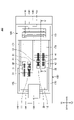
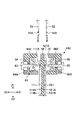
- FIG. 1 is a top view showing the semiconductor device according to the first embodiment.
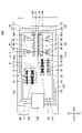
- FIG. 2 is a front view showing the semiconductor device according to the first embodiment;
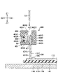
- FIG. 3 is a top view showing the relationship between the P terminal and N terminal and the circuit pattern in the semiconductor device according to the first embodiment.
- FIG. 4 is a cross-sectional view showing the relationship between the P terminal and N terminal and the circuit pattern in the semiconductor device according to the first embodiment.
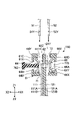
- FIG. 5 is a cross-sectional view (part 1) showing the terminal fixture in the semiconductor device according to the first embodiment.
- FIG. 6 is a cross-sectional view (part 2) showing the terminal fixture in the semiconductor device according to the first embodiment.
- FIG. 7 is a circuit diagram showing the semiconductor device according to the first embodiment.
- FIG. 8 is a cross-sectional view showing a terminal fixture to which first external terminals and second external terminals are fixed in the first embodiment.
- FIG. 9 is a cross-sectional view showing the semiconductor device according to the second embodiment.
- FIG. 10 is a cross-sectional view showing the semiconductor device according to the second embodiment.
- FIG. 11 is a cross-sectional view showing a semiconductor device according to the third embodiment.
- FIG. 12 is a top view showing the semiconductor device according to the fourth embodiment.
- FIG. 13 is a cross-sectional view (part 1) showing a terminal fixture for an O terminal in a semiconductor device according to a fourth embodiment;
- FIG. 14 is a cross-sectional view (part 2) showing the terminal fixture for the O terminal in the semiconductor device according to the fourth embodiment.
- FIG. 15 is a cross-sectional view showing a terminal fixture in a semiconductor device according to the fifth embodiment.
- FIG. 16 is a cross-sectional view showing a terminal fixture to which first external terminals and second external terminals are fixed in the fifth embodiment.
- FIG. 17 is a cross-sectional view showing a terminal fixture in a semiconductor device according to the sixth embodiment.
- FIG. 18 is a cross-sectional view showing a terminal fixture to which first external terminals and second external terminals are fixed in the sixth embodiment.
- FIG. 19 is a cross-sectional view showing a terminal fixture in a semiconductor device according to the seventh embodiment.
- FIG. 20 is a cross-sectional view showing a terminal fixture to which first external terminals and second external terminals are fixed in the seventh embodiment.
- FIG. 21 is a cross-sectional view showing a terminal fixture in a semiconductor device according to the eighth embodiment.
- FIG. 22 is a cross-sectional view showing a terminal fixture to which first external terminals and second external terminals are fixed in
- An object of the present disclosure is to provide a semiconductor device capable of reducing inductance in internal terminals.
- the inductance at the internal terminals can be reduced.
- a semiconductor device has a first main surface and a second main surface opposite to the first main surface, and has a first internal terminal to which a first external terminal is connected. a second internal terminal having a terminal, a third main surface, and a fourth main surface opposite to the third main surface, to which the second external terminal is connected; a semiconductor element connected between two internal terminals; a first pressing member pressing the first external terminal against the second principal surface; and a second pressing member pressing the second external terminal against the fourth principal surface. and a member, wherein the first main surface and the third main surface are parallel, and at least a portion of the first main surface and at least a portion of the third main surface face each other.
- the first main surface and the third main surface are parallel, and at least part of the first main surface and at least part of the third main surface face each other. Therefore, the current flowing through the flat plate portion of the first internal terminal and the current flowing through the flat plate portion of the second internal terminal flow in directions opposite to each other. The magnetic field around the flat plate portion of the internal terminal cancels each other out. Therefore, the difference in inductance between the P terminal and the N terminal is almost eliminated, and the inductance at the internal terminals can be reduced.
- the second main surface and the fourth main surface may be parallel to each other.
- the first external terminals and the second external terminals can be pressed from opposite directions, the first external terminals can be easily pressed against the second main surface and the second external terminals can be easily pressed against the fourth main surface.
- a circuit pattern provided with the semiconductor element is provided, and the first principal surface, the second principal surface, the third principal surface and the fourth principal surface are the It may be perpendicular to the circuit pattern. In this case, it is easy to bring the first external terminal and the second external terminal into contact with the first internal terminal and the second internal terminal from a direction perpendicular to the circuit pattern.
- a circuit pattern provided with the semiconductor element is provided, and the first principal surface, the second principal surface, the third principal surface and the fourth principal surface are the It may be parallel to the circuit pattern. In this case, it is easy to bring the first external terminal and the second external terminal into contact with the first internal terminal and the second internal terminal from a direction parallel to the circuit pattern.
- the first pressing member has a first bolt that presses the first external terminal against the second principal surface
- the second pressing member has the fourth
- a second bolt for pressing the second external terminal may be provided on the main surface. In this case, by tightening the first bolt and the second bolt, the first external terminal can be pressed against the second principal surface and the second external terminal can be pressed against the fourth principal surface.
- the first pressing member has a first cushioning member sandwiched between the first bolt and the first external terminal, and the second pressing member includes the second bolt and the second external terminal.
- the pressure applied from the first bolt to the first external terminal is dispersed by the first cushioning member
- the pressure applied from the second bolt to the second external terminal is dispersed by the second cushioning member.
- the first cushioning member has a first detent on the surface facing the second main surface
- the second cushioning member has a surface facing the fourth main surface. It may have a second detent.
- the adhesion strength between the first cushioning member and the second main surface and the adhesion strength between the second cushioning member and the fourth main surface can be improved.
- the first internal terminal has a first concave portion on the second main surface
- the second internal terminal has a second concave portion on the fourth main surface
- the first cushioning member may have a first projection that fits into the first recess
- the second cushioning member may have a second projection that fits into the second recess.
- the first protrusion fits into the first recess and the second protrusion fits into the second recess, whereby the first external terminal and the second external terminal are separated from the first internal terminal and the second internal terminal, respectively. It can be done easily.
- an insulating member is provided between the first internal terminal and the second internal terminal, and the first bolt penetrates the first internal terminal.
- a through hole may be formed, and a hole into which the first bolt passing through the through hole is fitted may be formed in the insulating member.
- the first bolt penetrates the through hole and fits into the hole of the insulating member, thereby making it difficult for the first external terminal to come off from the first internal terminal.
- a first through hole is formed in the first internal terminal
- a second through hole is formed in the second internal terminal
- the first pressing member A through hole and a bolt passing through the second through hole may be provided, and the second pressing member may have a nut fitted to the bolt.
- the bolt passes through the first through hole and the second through hole, and the nut is fitted to the bolt, so that the first external terminal and the second external terminal are not easily separated from the first internal terminal and the second internal terminal, respectively. can.
- the first pressing member may have a first leaf spring
- the second pressing member may have a second leaf spring.
- the first external terminal and the second external terminal can be connected to the semiconductor device by simple work.
- a third internal terminal having a fifth main surface and a sixth main surface opposite to the fifth main surface, to which a third external terminal is connected; and a third pressing member that presses the third external terminal on the sixth main surface, and the plurality of semiconductor elements are connected in series between the first internal terminal and the second internal terminal.
- the third internal terminal may be connected between two semiconductor elements of the plurality of semiconductor elements.
- the configuration around the third internal terminal becomes similar to the configuration around the first internal terminal and the second internal terminal, which facilitates the work of connecting the third external terminal to the third internal terminal.
- the semiconductor element may contain silicon, silicon carbide, or gallium nitride.
- a power module or the like can be configured by using a semiconductor element containing silicon, silicon carbide, or gallium nitride.
- a plane including the X1-X2 direction and the Y1-Y2 direction is the XY plane
- a plane including the Y1-Y2 direction and the Z1-Z2 direction is the YZ plane
- a plane including the Z1-Z2 direction and the X1-X2 direction is the ZX plane.
- the Z1 direction is defined as the upward direction
- the Z2 direction is defined as the downward direction.
- planar viewing means viewing an object from the Z1 side.
- FIG. 1 is a top view showing the semiconductor device according to the first embodiment.
- FIG. 2 is a front view showing the semiconductor device according to the first embodiment;
- FIG. 1 is a top view showing the semiconductor device according to the first embodiment.
- a semiconductor device 100 mainly has a P terminal 110, an N terminal 120, an O terminal 130, a base plate 140, a case 150, and a terminal fixture 160.
- the P terminal 110 is a positive power supply terminal
- the N terminal 120 is a negative power supply terminal
- the O terminal 130 is an output terminal.
- P terminal 110 , N terminal 120 , and O terminal 130 are attached to case 150 .
- the P terminal 110 is an example of a first internal terminal
- the N terminal 120 is an example of a second internal terminal
- the O terminal is an example of a third internal terminal.
- the X1-X2 direction is the direction along the long sides of the rectangular base plate 140 and the case 150 in plan view
- the Y1-Y2 direction is the direction along the short sides of the base plate 140 and the case 150
- the Z1-Z2 direction is the direction along the normal to the base plate 140 and the case 150 .
- the base plate 140 is, for example, a plate-like body that is rectangular in plan view and has a uniform thickness.
- the base plate 140 has a major surface 141 .
- the material of the base plate 140 is a metal having high thermal conductivity, such as copper (Cu), copper alloy, aluminum (Al), or the like.
- the base plate 140 is fixed to a cooler or the like using a thermal interface material (TIM) or the like.
- the case 150 is, for example, frame-shaped in plan view.
- the material of the case 150 is an insulator such as resin.
- the case 150 has a pair of side wall portions 151 and 152 facing each other, and a pair of end wall portions 153 and 154 connecting both ends of the side wall portions 151 and 152 .
- the side wall portions 151 and 152 are arranged parallel to the ZX plane, and the end wall portions 153 and 154 are arranged parallel to the YZ plane.
- the side wall portion 152 is arranged on the Y2 side of the side wall portion 151
- the end wall portion 154 is arranged on the X2 side of the end wall portion 153 .
- An insulating substrate 170 is arranged on the Z1 side of the base plate 140 . That is, the insulating substrate 170 is arranged on the main surface 141 of the base plate 140 .
- the insulating substrate 170 has a first circuit pattern 171, a second circuit pattern 172 and a third circuit pattern 173 on the Z1 side surface, and a conductive layer 179 on the Z2 side surface (see FIGS. 4 and 6).
- the first circuit pattern 171, the second circuit pattern 172 and the third circuit pattern 173 are parallel to the XY plane.
- a conductive layer 179 is bonded to the base plate 140 with a bonding material such as solder.
- a plurality of first transistors 11 and a plurality of first diodes 21 are mounted on the first circuit pattern 171 .
- a plurality of second transistors 12 and a plurality of second diodes 22 are mounted on the second circuit pattern 172 .
- the first transistor 11, the first diode 21, the second transistor 12 and the second diode 22 are examples of semiconductor elements.
- the first transistor 11 has a first gate electrode, a first source electrode and a first drain electrode.
- the first gate electrode and the first source electrode are arranged on the main surface of the first transistor 11 on the Z1 side, and the first drain electrode is arranged on the main surface on the Z2 side of the first transistor 11 .
- the first drain electrode is bonded to the first circuit pattern 171 with a bonding material such as solder.
- the first diode 21 has a first anode electrode and a first cathode electrode.
- the first anode electrode is arranged on the main surface of the first diode 21 on the Z1 side, and the first cathode electrode is arranged on the main surface on the Z2 side of the first diode 21 .
- the first cathode electrode is joined to the first circuit pattern 171 with a joining material such as solder.
- the second transistor 12 has a second gate electrode, a second source electrode and a second drain electrode.
- the second gate electrode and the second source electrode are arranged on the main surface of the second transistor 12 on the Z1 side, and the second drain electrode is arranged on the main surface on the Z2 side of the second transistor 12 .
- a second drain electrode is joined to the second circuit pattern 172 by a joining material such as solder.
- the second diode 22 has a second anode electrode and a second cathode electrode.
- the second anode electrode is arranged on the main surface of the second diode 22 on the Z1 side, and the second cathode electrode is arranged on the main surface on the Z2 side of the second diode 22 .
- a second cathode electrode is joined to the second circuit pattern 172 with a joining material such as solder.
- the semiconductor device 100 has multiple wires 31 , multiple wires 32 , multiple wires 41 , and multiple wires 42 .
- a wire 31 connects the first source electrode of the first transistor 11 and the second circuit pattern 172 .
- a wire 32 connects the first source electrode of the first transistor 11 and the first anode electrode of the first diode 21 .
- a wire 41 connects the second source electrode of the second transistor 12 and the third circuit pattern 173 .
- a wire 42 connects the second source electrode of the second transistor 12 and the second anode electrode of the second diode 22 .
- the semiconductor device 100 includes gate terminals, auxiliary source terminals, gate wires, auxiliary source wires, circuit patterns connecting the gate wires, circuit patterns connecting the auxiliary source wires, etc., but descriptions thereof will be omitted for convenience.
- illustration of the gate electrode is omitted in FIG. 1 and the like.
- FIG. 3 is a top view showing the relationship between the P terminal 110 and the N terminal 120 and the first circuit pattern 171 and the third circuit pattern 173 in the semiconductor device according to the first embodiment.
- FIG. 4 is a cross-sectional view showing the relationship between the P terminal 110 and N terminal 120 and the first circuit pattern 171 and third circuit pattern 173 in the semiconductor device according to the first embodiment.
- FIG. 4 corresponds to a cross-sectional view taken along line IV-IV in FIG. 3 and 4, the case 150 is omitted.
- the P terminal 110 has a flat plate portion 111 and a contact portion 112 .
- the flat plate portion 111 has a first principal surface 111A and a second principal surface 111B opposite to the first principal surface 111A.
- the first main surface 111A and the second main surface 111B are surfaces parallel to the YZ plane and perpendicular to the X1-X2 direction.
- the first main surface 111A and the second main surface 111B are surfaces perpendicular to the first circuit pattern 171, the second circuit pattern 172, and the third circuit pattern 173, respectively.
- the first main surface 111A is on the X1 side of the second main surface 111B.
- the flat plate portion 111 is separated from the first circuit pattern 171 and the third circuit pattern 173 on the Z1 side.
- the contact portion 112 extends from the Z2 side end of the flat plate portion 111 and is bent toward the X2 side.
- the contact portion 112 is connected to the first circuit pattern 171 via a bonding material such
- the N terminal 120 has a flat plate portion 121 and a contact portion 122 .
- the flat plate portion 121 has a third principal surface 121A and a fourth principal surface 121B opposite to the third principal surface 121A.
- the third main surface 121A and the fourth main surface 121B are surfaces parallel to the YZ plane and perpendicular to the X1-X2 direction.
- the third main surface 121A and the fourth main surface 121B are surfaces perpendicular to the first circuit pattern 171, the second circuit pattern 172, and the third circuit pattern 173, respectively.
- the third main surface 121A is on the X2 side of the fourth main surface 121B.
- the flat plate portion 121 is separated from the first circuit pattern 171 and the third circuit pattern 173 on the Z1 side.
- the contact portion 122 extends from the Z2 side end portion of the flat plate portion 121 and is bent toward the X2 side.
- the contact portion 122 is connected to the third circuit pattern 173 via a bonding material
- the flat plate portion 111 of the P terminal 110 is on the X2 side of the flat plate portion 121 of the N terminal 120 .
- 111 A of 1st main surfaces and 121 A of 3rd main surfaces are parallel, and 111 A of 1st main surfaces and 121 A of 3rd main surfaces mutually oppose.
- the flat plate portion 111 and the flat plate portion 121 overlap each other on the Z1 side of the insulating substrate 170 when viewed from the X1-X2 direction.
- the distance between the first major surface 111A and the third major surface 121A is preferably 5 mm or less, more preferably 3 mm or less.
- the O terminal 130 is connected to the second circuit pattern 172 via a bonding material such as solder.
- the O terminal 130 extends to the X2 side of the case 150 through the Z1 side of the end wall portion 154, for example.
- FIG. 5 and 6 are cross-sectional views showing the terminal fixture 160 in the semiconductor device according to the first embodiment.
- FIG. 5 corresponds to a cross-sectional view taken along line V-V in FIG.
- FIG. 6 corresponds to a cross-sectional view taken along line VI-VI in FIG.
- the case 150 is omitted.
- the terminal fixture 160 mainly has a housing 61 , a partition wall 62 , a first bolt 63 , a first pressing terminal 64 , a second bolt 65 and a second pressing terminal 66 .
- the housing 61 is fixed to the case 150, for example.
- the housing 61 is in contact with, for example, the side wall portion 151 , the side wall portion 152 and the end wall portion 153 and is separated from the end wall portion 154 .
- the housing 61 has a rectangular parallelepiped external shape including a lower wall portion 61A, an upper wall portion 61B, a side wall portion 61C, a side wall portion 61D, a side wall portion 61E, and a side wall portion 61F.
- the lower wall portion 61A and upper wall portion 61B are parallel to the XY plane
- the side wall portions 61C and 61D are parallel to the YZ plane
- the side wall portions 61E and 61F are parallel to the ZX plane.
- the upper wall portion 61B is located on the Z1 side of the lower wall portion 61A.
- the side wall portion 61C is located on the X2 side of the side wall portion 61D.
- the side wall portion 61E is on the Y2 side of the side wall portion 61F.
- An opening 71 is formed in the center of the lower wall portion 61A in the X1-X2 direction.
- a flat plate portion 111 of the P terminal 110 and a flat plate portion 121 of the N terminal 120 extend through the opening 71 into the housing 61 .
- Partition wall 62 is provided between flat plate portion 111 and flat plate portion 121 .
- the partition wall 62 is connected to the side wall portion 61E and the side wall portion 61F.
- a metal plate 62A is provided on the surface of the partition wall 62 facing the upper end of the flat plate portion 111, and a metal plate 62B is provided on the surface of the partition wall 62 facing the upper end of the flat plate portion 121. As shown in FIG.
- the metal plate 62A and the metal plate 62B are made of metal having high buckling strength such as steel.
- a surface 62C of the metal plate 62A facing the first main surface 111A of the flat plate portion 111 may be subjected to anti-rotation processing such as knurling.
- a surface 62D of the metal plate 62B facing the third main surface 121A of the flat plate portion 121 may be subjected to anti-rotation processing such as knurling.
- An opening 72 is formed in the center of the upper wall portion 61B in the X1-X2 direction.
- a first external terminal 51 connected to the P terminal 110 and a second external terminal 52 connected to the N terminal 120 are inserted into the housing 61 through the opening 72 .
- the shape of the first external terminal 51 and the second external terminal 52 is, for example, a plate shape.
- a first bolt hole 81A is formed in the side wall portion 61C, and a first female screw 82A is provided in the first bolt hole 81A.
- the first female screw 82A is made of a metal having high buckling strength such as steel.
- the first bolt 63 is fitted into the first female thread 82A so that the head of the first bolt 63 is located on the X2 side of the side wall portion 61C.
- a tip surface 63X of the first bolt 63 faces the second main surface 111B of the flat plate portion 111. As shown in FIG.
- the metal plate 62A is provided so as to overlap the tip surface 63X of the first bolt 63 when viewed from the X1-X2 direction.
- the first bolt 63 is, for example, a hexagon socket bolt.
- a first pressing terminal 64 is arranged between the tip surface 63X of the first bolt 63 and the second main surface 111B of the flat plate portion 111 .
- the first pressing terminal 64 is provided so as to be movable in the X1-X2 direction as the first bolt 63 is tightened and loosened.
- the first pressing terminal 64 is sandwiched between the first bolt 63 and the first external terminal 51 when the first external terminal 51 is inserted into the housing 61 .
- the first pressing terminal 64 is made of a metal having high buckling strength, such as steel.
- the first pressing terminal 64 is made of, for example, a metal plate.
- the surface 64X of the first pressing terminal 64 facing the second main surface 111B of the flat plate portion 111 may be subjected to anti-rotation processing such as knurling.
- the first pressing terminal 64 may have a first detent 91 on the surface 64X.
- the first pressing terminal 64 is provided at the end on the Z1 side so as to guide the tip of the first external terminal 51 between the tip end surface 63X of the first bolt 63 and the second main surface 111B of the flat plate portion 111 . You may have the inclined surface 64Y inclined from the main surface 111B.
- the first pressing terminal 64 is an example of a first cushioning member.
- a first pressing member 67 includes a first bolt 63 and a first pressing terminal 64 .
- a plurality of sets, for example two sets, of the first bolt 63, the first bolt hole 81A and the first female screw 82A may be provided.
- a plurality of first pressing terminals 64 may be provided so as to correspond to each of the plurality of sets, or only one may be provided in common to the plurality of sets.
- a second bolt hole 81B is formed in the side wall portion 61D, and a second female screw 82B is provided in the second bolt hole 81B.
- the second female screw 82B is made of a metal having high buckling strength such as steel.
- the second bolt 65 is fitted into the second female thread 82B so that the head of the second bolt 65 is positioned on the X1 side of the side wall portion 61D.
- a tip surface 65X of the second bolt 65 faces the fourth main surface 121B of the flat plate portion 121.
- the metal plate 62B is provided so as to overlap the tip surface 65X of the second bolt 65 when viewed from the X1-X2 direction.
- the second bolt 65 is, for example, a hexagon socket bolt.
- An opening (not shown) for tightening and loosening the second bolt 65 is formed in the end wall portion 153 .
- a second pressing terminal 66 is arranged between the tip end surface 65X of the second bolt 65 and the fourth main surface 121B of the flat plate portion 121 .
- the second pressing terminal 66 is provided so as to be movable in the X1-X2 direction as the second bolt 65 is tightened and loosened.
- the second pressing terminal 66 is sandwiched between the second bolt 65 and the second external terminal 52 when the second external terminal 52 is inserted into the housing 61 .
- the second pressing terminal 66 is made of metal such as steel having high buckling strength.
- the second pressing terminal 66 is made of, for example, a metal plate.
- the surface 66X of the second pressing terminal 66 facing the fourth main surface 121B of the flat plate portion 121 may be subjected to anti-rotation processing such as knurling.
- the second push terminal 66 may have a second detent 92 on the surface 66X.
- the second pressing terminal 66 is provided at the end on the Z1 side so as to guide the tip of the second external terminal 52 between the tip surface 65X of the second bolt 65 and the fourth main surface 121B of the flat plate portion 121. You may have the inclined surface 66Y inclined from the main surface 121B.
- the second pressing terminal 66 is an example of a second cushioning member.
- a second bolt 65 and a second pressing terminal 66 are included in the second pressing member 68 .
- a plurality of sets, for example two sets, of the second bolt 65, the second bolt hole 81B and the second female screw 82B may be provided.
- a plurality of second pressing terminals 66 may be provided so as to correspond to each of the plurality of sets, or only one second pressing terminal 66 may be provided in common to the plurality of sets.
- the housing 61 and the partition wall 62 are made of resin such as polyphenylene sulfide (PPS), and may be resin molded products.
- the metal plate 62A and the metal plate 62B may be insert-molded in the partition wall 62 .
- FIG. 7 is a circuit diagram showing the semiconductor device according to the first embodiment.
- the first drain electrode of the first transistor 11 and the first cathode electrode of the first diode 21 are connected to the P terminal 110 via the first circuit pattern 171 .
- the source electrode of the first transistor 11 is connected to the O terminal 130 via the second circuit pattern 172 and the wire 31 , and the first anode electrode of the first diode 21 is connected via the wire 32 .
- the first drain electrode of the first transistor 11 and the first cathode electrode of the first diode 21 are commonly connected to the P terminal 110, and the first source electrode of the first transistor 11 and the first cathode electrode of the first diode 21 are connected in common.
- 1 anode electrode is commonly connected to the O terminal 130 . That is, the first transistor 11 and the first diode 21 are connected in parallel between the P terminal 110 and the O terminal 130 .
- a second drain electrode of the second transistor 12 and a second cathode electrode of the second diode 22 are connected to the O terminal 130 via the second circuit pattern 172 .
- the source electrode of the second transistor 12 is connected to the N terminal 120 via the third circuit pattern 173 and the wire 41
- the second anode electrode of the second diode 22 is connected via the wire 42 .
- the second drain electrode of the second transistor 12 and the second cathode electrode of the second diode 22 are commonly connected to the O terminal 130
- the second source electrode of the second transistor 12 and the second cathode electrode of the second diode 22 are connected in common.
- 2 anode electrodes are commonly connected to the N terminal 120 . That is, the second transistor 12 and the second diode 22 are connected in parallel between the O terminal 130 and the N terminal 120 .
- the upper arm 1 includes a first transistor 11 and a first diode 21.
- Lower arm 2 includes second transistor 12 and second diode 22 .
- Upper arm 1 and lower arm 2 are connected in series between P terminal 110 and N terminal 120 .
- FIG. 8 is a cross-sectional view showing the terminal fixture 160 to which the first external terminal 51 and the second external terminal 52 are fixed in the first embodiment.
- the first bolt 63 is loosened, and a gap between the surface 64X of the first pressing terminal 64 and the second main surface 111B is secured. , form a gap larger than the thickness of the first external terminal 51 .
- the second bolt 65 is loosened to form a gap larger than the thickness of the second external terminal 52 between the surface 66X of the second pressing terminal 66 and the fourth main surface 121B.
- the first bolt 63 is inserted between the surface 64X of the first pressing terminal 64 and the second main surface 111B of the flat plate portion 111 while the first external terminal 51 is aligned along the inclined surface 64Y of the first pressing terminal 64. is inserted up to the Z2 side of the tip end surface 63X.
- the second bolt 65 is inserted between the surface 66X of the second pressing terminal 66 and the fourth main surface 121B of the flat plate portion 121 while the second external terminal 52 is aligned along the inclined surface 66Y of the second pressing terminal 66. is inserted up to the Z2 side of the tip end surface 65X.
- the first external terminal 51 is pressed against the flat plate portion 111 via the first pressing terminal 64 .
- the second external terminal 52 is pressed against the flat plate portion 121 via the second pressing terminal 66 .
- the first external terminal 51 is fixed to the P terminal 110
- the second external terminal 52 is fixed to the N terminal 120
- the first external terminal 51 and the second external terminal 52 can be connected to the semiconductor device 100.
- the current flowing through the flat plate portion 111 of the P terminal 110 and the current flowing through the flat plate portion 121 of the N terminal 120 flow in opposite directions. Therefore, the magnetic field around the flat plate portion 111 and the magnetic field around the flat plate portion 121 cancel each other out. Therefore, according to the present embodiment, the magnetic fields cancel each other over a wide range of the P terminal 110 and the N terminal 120, and the inductance at the P terminal 110 and the N terminal 120 can be reduced.
- first main surface 111A, the second main surface 111B, the third main surface 121A and the fourth main surface 121B are perpendicular to the first circuit pattern 171 and the third circuit pattern 173, they are perpendicular to the main surface 141 of the base plate 140.
- the first external terminal 51 and the second external terminal 52 can be inserted into the terminal fixture 160 from any direction. Therefore, it is easy to bring the first external terminal 51 and the second external terminal 52 into contact with the P terminal 110 and the N terminal 120, respectively.
- the first pressing member 67 includes the first bolt 63 and the second pressing member 68 includes the second bolt 65
- the second main surface 111B is provided with the first external force.
- the terminal 51 can be firmly pressed, and the second external terminal 52 can be firmly pressed against the fourth main surface 121B.
- the second main surface 111B and the fourth main surface 121B are parallel to each other, the first external terminal 51 and the second external terminal 52 can be pressed from opposite directions. Therefore, the first external terminal 51 can be easily pressed against the second main surface 111B, and the second external terminal 52 can be easily pressed against the fourth main surface 121B.
- the first pressing terminal 64 is sandwiched between the first bolt 63 and the first external terminal 51
- the second pressing terminal 66 is sandwiched between the second bolt 65 and the second external terminal 52 . Therefore, the pressure applied from the first bolt 63 to the first external terminal 51 is dispersed by the first pressing terminal 64
- the pressure applied from the second bolt 65 to the second external terminal 52 is dispersed by the second pressing terminal 66 .
- the current tends to concentrate in areas where the contact pressure is strong, but by dispersing the pressure by the first pressing terminals 64 and the second pressing terminals 66, the concentration of the current can be alleviated and the heat generated due to the concentration of the current can be suppressed.
- the adhesion strength between the first pressing terminal 64 and the second main surface 111B can be improved.
- the adhesion strength between the second pressing terminal 66 and the fourth main surface 121B can be improved.
- FIG. 9 is a cross-sectional view showing the semiconductor device according to the second embodiment.
- FIG. 10 is a cross-sectional view showing the semiconductor device according to the second embodiment.
- FIG. 9 corresponds to a cross-sectional view at a position in the Z1-Z2 direction similar to FIG.
- FIG. 10 corresponds to a cross-sectional view taken along line XX in FIG.
- the housing 61, the partition wall 62, the metal plate 62A and the metal plate 62B are omitted.
- the case 150 is omitted.
- the first main surface 111A and the second main surface 111B of the P terminal 110 are surfaces parallel to the ZX plane and perpendicular to the Y1-Y2 direction.
- the first main surface 111A and the second main surface 111B are surfaces perpendicular to the first circuit pattern 171, the second circuit pattern 172, and the third circuit pattern 173, respectively.
- the first main surface 111A is on the Y2 side of the second main surface 111B.
- the flat plate portion 111 is separated from the first circuit pattern 171 on the Z1 side.
- the contact portion 112 extends from the Z2 side end portion of the flat plate portion 111 and is bent toward the Y1 side.
- the contact portion 112 is connected to the first circuit pattern 171 via a bonding material such as solder.
- the third main surface 121A and the fourth main surface 121B of the N terminal 120 are surfaces parallel to the ZX plane and perpendicular to the Y1-Y2 direction.
- the third main surface 121A and the fourth main surface 121B are surfaces perpendicular to the first circuit pattern 171, the second circuit pattern 172, and the third circuit pattern 173, respectively.
- the third main surface 121A is on the Y1 side of the fourth main surface 121B.
- the flat plate portion 121 is separated from the third circuit pattern 173 on the Z1 side.
- the contact portion 122 extends from the Z2 side end of the flat plate portion 121 and is bent toward the Y2 side.
- the contact portion 122 is connected to the third circuit pattern 173 via a bonding material such as solder.
- the flat plate portion 111 of the P terminal 110 is on the Y1 side of the flat plate portion 121 of the N terminal 120 .
- 111 A of 1st main surfaces and 121 A of 3rd main surfaces are parallel, and 111 A of 1st main surfaces and 121 A of 3rd main surfaces mutually oppose.
- the flat plate portion 111 and the flat plate portion 121 overlap each other on the Z1 side of the insulating substrate 170 when viewed from the Y1-Y2 direction.
- the flat plate portion 111 and the flat plate portion 121 are arranged in the X1-X2 direction, whereas in the second embodiment, the flat plate portion 111 and the flat plate portion 121 are arranged in the Y1-Y2 direction. I'm in. Along with this, the orientation of the terminal fixture 160 is rotated by 90° within the XY plane from that of the first embodiment.
- FIG. 11 is a cross-sectional view showing a semiconductor device according to the third embodiment.
- FIG. 11, like FIG. 5, corresponds to a cross-sectional view taken along line VV in FIG. In FIG. 10, the case 150 is omitted.
- a semiconductor device 300 according to the third embodiment has a P terminal 310 instead of the P terminal 110 and an N terminal 320 instead of the N terminal 120 .
- the P terminal 310 has a flat plate portion 311 , a contact portion 312 and a connecting portion 313 .
- the flat plate portion 311 has a first principal surface 311A and a second principal surface 311B opposite to the first principal surface 311A.
- the first main surface 311A and the second main surface 311B are surfaces parallel to the XY plane and perpendicular to the Z1-Z2 direction.
- the first main surface 311A and the second main surface 311B are surfaces parallel to the first circuit pattern 171 , the second circuit pattern 172 and the third circuit pattern 173 .
- the first main surface 311A is on the Z2 side of the second main surface 311B.
- the flat plate portion 311 is separated from the first circuit pattern 171 and the third circuit pattern 173 on the Z1 side.
- the contact portion 312 is connected to the first circuit pattern 171 via a bonding material such as solder.
- the connecting portion 313 extends from the X2 side end of the flat plate portion 311 to the Z2 side, and extends from the X1 side end of the contact portion 312 to the Z1 side.
- the connecting portion 313 connects the flat plate portion 311 and the contact portion 312 .
- the N terminal 320 has a flat plate portion 321 , a contact portion 322 and a connecting portion 323 .
- the flat plate portion 321 has a third principal surface 321A and a fourth principal surface 321B opposite to the third principal surface 321A.
- the third main surface 321A and the fourth main surface 321B are surfaces parallel to the XY plane and perpendicular to the Z1-Z2 direction.
- the third main surface 321A and the fourth main surface 321B are surfaces parallel to the first circuit pattern 171, the second circuit pattern 172 and the third circuit pattern 173. As shown in FIG.
- the third main surface 321A is on the Z1 side of the fourth main surface 321B.
- the flat plate portion 321 is separated from the first circuit pattern 171 and the third circuit pattern 173 on the Z1 side.
- the contact portion 322 is connected to the third circuit pattern 173 via a bonding material such as solder.
- the connecting portion 323 extends from the X2 side end of the flat plate portion 321 to the Z2 side, and extends from the X1 side end of the contact portion 322 to the Z1 side.
- the connecting portion 323 connects the flat plate portion 321 and the contact portion 322 .
- the flat plate portion 111 and the flat plate portion 121 are arranged in the X1-X2 direction, whereas in the third embodiment, the flat plate portion 111 and the flat plate portion 121 are arranged in the Z1-Z2 direction. I'm in. Along with this, the orientation of the terminal fixture 160 is rotated by 90° within the ZX plane from that of the first embodiment.
- the same effect as the first embodiment can be obtained by the third embodiment.
- the first principal surface 111A, the second principal surface 111B, the third principal surface 121A and the fourth principal surface 121B are parallel to the first circuit pattern 171 and the third circuit pattern 173, the principal surface 141 of the base plate 140
- the first external terminal 51 and the second external terminal 52 can be inserted into the terminal fixture 160 from a direction parallel to . Therefore, it is easy to bring the first external terminal 51 and the second external terminal 52 into contact with the P terminal 110 and the N terminal 120, respectively.
- FIG. 12 is a top view showing the semiconductor device according to the fourth embodiment.
- 13 and 14 are cross-sectional views showing a terminal fixture for an O terminal in a semiconductor device according to the fourth embodiment.
- FIG. 13 corresponds to a cross-sectional view taken along line VV in FIG.
- FIG. 14 corresponds to a cross-sectional view at a position in the Z1-Z2 direction similar to FIG. In FIG. 13, the case 150 is omitted.
- a semiconductor device 400 according to the fourth embodiment mainly has a P terminal 110, an N terminal 120, an O terminal 130, a base plate 140, a case 150, a terminal fixture 160, and a terminal fixture 460. .
- the O terminal 130 has a flat plate portion 131 and a contact portion 132 .
- the flat plate portion 131 has a fifth main surface 131A and a sixth main surface 131B opposite to the fifth main surface 131A.
- the fifth main surface 131A and the sixth main surface 131B are surfaces parallel to the YZ plane and perpendicular to the X1-X2 direction.
- the fifth main surface 131A and the sixth main surface 131B are surfaces perpendicular to the first circuit pattern 171, the second circuit pattern 172, and the third circuit pattern 173, respectively.
- the fifth main surface 131A is on the X1 side of the sixth main surface 131B.
- the flat plate portion 131 is separated from the second circuit pattern 172 on the Z1 side.
- the contact portion 132 extends from the Z2 side end of the flat plate portion 131 and is bent toward the X1 side.
- the contact portion 132 is connected to the second circuit pattern 172 via a bonding material such as solder.
- the terminal fixture 460 mainly has a housing 461 , a third bolt 463 and a third pressing terminal 464 .
- the housing 461 is fixed to the case 150, for example.
- the housing 461 is in contact with, for example, the side wall portion 151 , the side wall portion 152 , and the end wall portion 154 and is separated from the end wall portion 153 .
- the housing 461 has a rectangular parallelepiped external shape including a lower wall portion 461A, an upper wall portion 461B, a side wall portion 461C, a side wall portion 461D, a side wall portion 461E, and a side wall portion 461F.
- the lower wall portion 461A and the upper wall portion 461B are parallel to the XY plane, the side wall portions 461C and 461D are parallel to the YZ plane, and the side wall portions 461E and 461F are parallel to the ZX plane.
- the upper wall portion 461B is located on the Z1 side of the lower wall portion 461A.
- the side wall portion 461C is on the X2 side of the side wall portion 461D.
- the side wall portion 461E is on the Y2 side of the side wall portion 461F.
- An opening 471 is formed in the lower wall portion 461A.
- a flat plate portion 131 of the O terminal 130 extends to the inside of the housing 461 through the opening 471 .
- a metal plate 462A is provided on a surface of the side wall portion 461D that faces the upper end of the flat plate portion 131 .
- the metal plate 462A is made of a metal having high buckling strength such as steel.
- a surface 462C of the metal plate 462A facing the fifth main surface 131A of the flat plate portion 131 may be subjected to anti-rotation processing such as knurling.
- An opening 472 is formed in the upper wall portion 461B.
- a third external terminal 53 connected to the O terminal 130 is inserted into the housing 461 through the opening 472 .
- the shape of the third external terminal 53 is, for example, a plate shape.
- a third bolt hole 481A is formed in the side wall portion 461C, and a third female screw 482A is provided in the third bolt hole 481A.
- the third female screw 482A is made of a metal having high buckling strength such as steel.
- the third bolt 463 is fitted into the third female screw 482A so that the head of the third bolt 463 is positioned on the X2 side of the side wall portion 461C.
- a tip surface 463X of the third bolt 463 faces the sixth main surface 131B of the flat plate portion 131 .
- the metal plate 462A is provided so as to overlap the tip surface 463X of the third bolt 463 when viewed from the X1-X2 direction.
- the third bolt 463 is, for example, a hexagon socket bolt. An opening (not shown) for tightening and loosening the third bolt 463 is formed in the end wall portion 154 .
- a third pressing terminal 464 is arranged between the tip surface 463X of the third bolt 463 and the sixth main surface 131B of the flat plate portion 131 .
- the third pressing terminal 464 is provided so as to be movable in the X1-X2 direction as the third bolt 463 is tightened and loosened.
- the third pressing terminal 464 is sandwiched between the third bolt 463 and the third external terminal 53 when the third external terminal 53 is inserted into the housing 61 .
- the third pressing terminal 464 is made of metal such as steel having high buckling strength.
- the third pressing terminal 464 is made of, for example, a metal plate.
- a surface 464X of the third pressing terminal 464 facing the sixth main surface 131B of the flat plate portion 131 may be subjected to anti-rotation processing such as knurling.
- the third push terminal 464 may have a third detent 93 on the surface 464X.
- the third pressing terminal 464 is provided at the end on the Z1 side so as to guide the tip of the third external terminal 53 between the tip surface 463X of the third bolt 463 and the sixth main surface 131B of the flat plate portion 131 . It may have an inclined surface 464Y inclined from the main surface 131B.
- the third pressing terminal 464 is an example of a third cushioning member.
- a third bolt 463 and a third pressing terminal 464 are included in the third pressing member 467 .
- a plurality of sets, for example two sets, of the third bolt 463, the third bolt hole 481A and the third female screw 482A may be provided.
- a plurality of third pressing terminals 464 may be provided so as to correspond to each of the plurality of sets, or only one third pressing terminal 464 may be provided in common to the plurality of sets.
- the housing 461 is made of resin such as polyphenylene sulfide (PPS), and may be a resin molded product.
- the metal plate 462A may be insert-molded into the side wall portion 461D.
- the third bolt 463 is tightened between the surface 464X of the third pressing terminal 464 and the sixth main surface 131B of the flat plate portion 131. is pushed to the Z2 side of the tip surface 463X.
- the third external terminal 53 can be fixed to the O terminal 130 and connected to the semiconductor device 100 .
- the configuration around the O terminal 130 becomes similar to the configuration around the P terminal 110 and the N terminal 120, so that the work of connecting the third external terminal 53 to the O terminal 130 can be facilitated.
- FIG. 15 is a cross-sectional view showing a terminal fixture in a semiconductor device according to the fifth embodiment.
- the first pressing terminal 64 has a columnar first protrusion 64Z that protrudes from the surface 64X toward the X1 side.
- the second pressing terminal 66 has a columnar second protrusion 66Z that protrudes from the surface 66X toward the X2 side.
- the flat plate portion 111 is formed with a first concave portion 111X into which the first convex portion 64Z is fitted, and the first external terminal 51 is formed with a through hole 51X through which the first convex portion 64Z penetrates.
- the flat plate portion 131 is formed with a second concave portion 121X into which the second convex portion 66Z is fitted, and the second external terminal 52 is formed with a through hole 52X through which the second convex portion 66Z penetrates.
- the length of the first protrusion 64Z that is, the dimension in the X1-X2 direction is approximately the same as the sum of the thickness of the first external terminal 51 and the depth of the first recess 111X.
- the length of the second protrusion 66Z that is, the dimension in the X1-X2 direction is approximately the same as the sum of the thickness of the second external terminal 52 and the depth of the second recess 121X.
- the metal plate 62A and the metal plate 62B may not be provided on the partition wall 62.
- FIG. 16 is a cross-sectional view showing the terminal fixture 160 to which the first external terminals 51 and the second external terminals 52 are fixed in the fifth embodiment.
- the first bolt 63 is loosened, and the first protrusion 64Z of the first pressing terminal 64 and the second main surface 111B are aligned. A gap larger than the thickness of the first external terminal 51 is formed between them.
- the second bolt 65 is loosened to form a gap larger than the thickness of the second external terminal 52 between the second projection 66Z of the second pressing terminal 66 and the fourth main surface 121B.
- the first external terminal 51 is inserted between the first projection 64Z and the second main surface 111B of the flat plate portion 111 so that the through hole 51X is aligned with the first recess 111X in the X1-X2 direction.
- the second external terminal 52 is inserted between the second convex portion 66Z and the fourth main surface 121B of the flat plate portion 121 so that the through hole 52X is aligned with the second concave portion 121X in the X1-X2 direction.
- Alignment portions such as spacers may be provided in the housing 61 so that the through holes 51X are aligned with the first recesses 111X and the through holes 52X are aligned with the second recesses 121X in a self-aligning manner.
- the first protrusion 64Z is inserted into the through-hole 51X and fitted into the first recess 111X. Press to 111.
- the second protrusion 66Z is inserted into the through hole 52X, and while being fitted into the second recess 121X, the second external terminal 52 is attached to the flat plate portion via the second pressing terminal 66. Press 121.
- the first external terminal 51 is fixed to the P terminal 110
- the second external terminal 52 is fixed to the N terminal 120
- the first external terminal 51 and the second external terminal 52 can be connected to the semiconductor device 100.
- the same effect as the first embodiment can be obtained by the fifth embodiment. Further, since the movement of the first external terminal 51 and the second external terminal 52 in the Z1-Z2 direction is restrained, the first external terminal 51 and the second external terminal 52 are removed from the P terminal 110 and the N terminal 120, respectively. It can be done easily.
- first recess 111X may be a through hole penetrating the flat plate portion 111
- second recess 121X may be a through hole penetrating the flat plate portion 121.
- FIG. 17 is a cross-sectional view showing a terminal fixture in a semiconductor device according to the sixth embodiment.
- a through hole 61X having a size through which the head of the first bolt 63 can pass is formed in the side wall portion 61C instead of the first bolt hole 81A, and the first female screw 82A is provided.
- a through hole 64 ⁇ /b>A through which the shaft portion of the first bolt 63 passes is formed in the first pressing terminal 64 .
- a through hole 111Y through which the shaft portion of the first bolt 63 passes is formed in the flat plate portion 111, and a through hole 51Y through which the shaft portion of the first bolt 63 passes is formed in the first external terminal 51.
- a bolt hole 62X is formed in the partition wall 62, and a female screw 62Y is provided in the bolt hole 62X.
- the internal thread 32Y is made of a metal having high buckling strength such as steel.
- An insulating paper 69 is arranged between the bolt hole 62X and the female screw 62Y and the flat plate portion 121.
- the partition wall 62 is not provided with the metal plate 62A and the metal plate 62B.
- the partition wall 62 is an example of an insulating member
- the bolt hole 62X is an example of a hole into which a first bolt is fitted.
- FIG. 18 is a cross-sectional view showing the terminal fixture 160 to which the first external terminals 51 and the second external terminals 52 are fixed in the sixth embodiment.
- the first bolt 63 is removed from the female screw 62Y, and the surface 64X of the first pressing terminal 64 and the second pressing terminal 64 are separated from each other.
- a gap larger than the thickness of the first external terminal 51 is formed between the principal surface 111B.
- the second bolt 65 is loosened to form a gap larger than the thickness of the second external terminal 52 between the surface 66X of the second pressing terminal 66 and the fourth main surface 121B.
- the X1-X2 direction is inserted so that the through hole 51Y is aligned with the through hole 111Y.
- the second external terminal 52 is aligned with the inclined surface 66Y of the second pressing terminal 66
- the second bolt 65 is inserted between the surface 66X of the second pressing terminal 66 and the fourth main surface 121B of the flat plate portion 121. Insert up to the Z2 side of the tip surface 65X.
- a positioning portion such as a spacer may be provided in the housing 61 so that the through hole 51Y is aligned with the through hole 111Y in a self-aligning manner.
- the first bolt 63 is inserted into the through hole 64A, the through hole 51Y, and the through hole 111Y.
- the first external terminal 51 is pressed against the flat plate portion 111 .
- the second external terminal 52 is pressed against the flat plate portion 121 via the second pressing terminal 66 .
- the first external terminal 51 is fixed to the P terminal 110
- the second external terminal 52 is fixed to the N terminal 120
- the first external terminal 51 and the second external terminal 52 can be connected to the semiconductor device 100.
- the insulating paper 69 is provided, the first bolt 63 is electrically insulated from the N terminal 120 .
- an electrically insulating material such as resin or ceramic may be used as the material of the first bolt 63 while keeping the female screw 62Y from contacting the flat plate portion 121 .
- the insulating paper 69 may not be provided.
- the configuration on the P terminal 110 side and the configuration on the N terminal 120 side may be interchanged.
- the second external terminal 52 can be made difficult to come off from the N terminal 120 .
- FIG. 19 is a cross-sectional view showing a terminal fixture in a semiconductor device according to the seventh embodiment.
- a through hole 61X having a size through which the head of the first bolt 63 can pass is formed in the side wall portion 61C instead of the first bolt hole 81A, and the first female screw 82A is provided.
- a through hole 64A through which the shaft portion of the first bolt 63 passes is formed in the first pressing terminal 64.
- a through hole 111Y through which the shaft portion of the first bolt 63 passes is formed in the flat plate portion 111, and a through hole 51Y through which the shaft portion of the first bolt 63 passes is formed in the first external terminal 51.
- FIG. A through hole 62Z through which the shaft portion of the first bolt 63 passes is formed in the partition wall 62 .
- a through hole 121Y through which the shaft of the first bolt 63 passes is formed in the flat plate portion 121, and a through hole 52Y through which the shaft of the first bolt 63 passes is formed in the second external terminal 52.
- a through hole 66A through which the shaft portion of the first bolt 63 passes is formed in the second pressing terminal 66.
- the partition wall 62 is not provided with the metal plate 62A and the metal plate 62B.
- the through-hole 111Y is an example of a first through-hole
- the through-hole 121Y is an example of a second through-hole.
- a nut 75 into which the first bolt 63 is fitted is arranged on the X1 side of the second pressing terminal 66 .
- the side wall portion 61D is formed with a through hole 61Y having a size through which the nut 75 can pass, and the second female screw 82B is not provided.
- the nut 75 is an example of a second pressing member.
- the material of the first bolt 63 is an electrically insulating material such as resin or ceramic.
- the material of the nut 75 may be the same material as the material of the first bolt 63 .
- FIG. 20 is a cross-sectional view showing the terminal fixture 160 to which the first external terminals 51 and the second external terminals 52 are fixed in the seventh embodiment.
- the first bolt 63 is removed from the nut 75, and the surface 64X of the first pressing terminal 64 and the second A gap larger than the thickness of the first external terminal 51 is formed between the main surface 111B and a gap larger than the thickness of the second external terminal 52 between the surface 66X of the second pressing terminal 66 and the fourth main surface 121B. form a large gap.
- the X1-X2 direction is inserted so that the through hole 51Y is aligned with the through hole 111Y.
- the second external terminal 52 is aligned with the inclined surface 66Y of the second pressing terminal 66
- a contact is placed between the surface 66X of the second pressing terminal 66 and the fourth main surface 121B of the flat plate portion 121 in the X1-X2 direction.
- the through hole 52Y is inserted so as to line up with the through hole 121Y.
- Alignment portions such as spacers may be provided in the housing 61 so that the through holes 51Y are aligned with the through holes 111Y and the through holes 52Y are aligned with the through holes 121Y in a self-aligning manner.
- the first bolt 63 is inserted into the through hole 64A, the through hole 51Y, the through hole 111Y, the through hole 62Z, the through hole 121Y, and the through hole 66A, and the first bolt 63 and the nut 75 are screwed together.
- the first external terminal 51 is pressed against the flat plate portion 111 via the first pressing terminal 64
- the second external terminal 52 is pressed against the flat plate portion 121 via the second pressing terminal 66 .
- the first external terminal 51 is fixed to the P terminal 110
- the second external terminal 52 is fixed to the N terminal 120
- the first external terminal 51 and the second external terminal 52 can be connected to the semiconductor device 100.
- the seventh embodiment also provides the same effects as the first embodiment. Further, since the movement of the first external terminal 51 and the second external terminal 52 in the Z1-Z2 direction is restrained, the first external terminal 51 and the second external terminal 52 are removed from the P terminal 110 and the N terminal 120, respectively. It can be done easily.
- FIG. 21 is a cross-sectional view showing a terminal fixture in a semiconductor device according to the eighth embodiment.
- openings 871 and 873 are formed in the lower wall portion 61A instead of the opening 71.
- Flat plate portion 111 of P terminal 110 extends into housing 61 through opening 871
- flat plate portion 121 of N terminal 120 extends into housing 61 through opening 873 .
- An opening 872 and an opening 874 are formed instead of the opening 72 in the upper wall portion 61B. In the Z1-Z2 direction, the openings 871 and 872 overlap, and the openings 873 and 874 overlap.
- the partition wall 62 is not provided with the metal plate 62A and the metal plate 62B. Also, the first bolt 63, the first pressing terminal 64, the first bolt hole 81A, the first female screw 82A, the second bolt 65, the second pressing terminal 66, the second bolt hole 81B and the second female screw 82B are not provided. .
- a leaf spring 801, a leaf spring 802, a leaf spring 803, and a leaf spring 804 are arranged between the partition wall 62 and the side wall portion 61C.
- Leaf springs 801 and 802 extend from the lower wall portion 61A toward the Z1 side.
- the leaf springs 803 and 804 extend from the upper wall portion 61B to the Z2 side.
- the leaf springs 801 and 803 are arranged closer to the partition wall 62 than the openings 871 and 872, contact the first main surface 111A of the flat plate portion 111, and bias the flat plate portion 111 toward the X2 side.
- the leaf springs 802 and 804 are arranged closer to the side wall portion 61C than the openings 871 and 872, and the distance between the leaf springs 802 and 804 and the second main surface 111B of the flat plate portion 111 in a natural state is It is smaller than the thickness of the first external terminal 51 .
- Leaf springs 801 to 804 are examples of first leaf springs.
- a leaf spring 805, a leaf spring 806, a leaf spring 807, and a leaf spring 808 are arranged between the partition wall 62 and the side wall portion 61D.
- Leaf springs 805 and 806 extend from the lower wall portion 61A to the Z1 side.
- Leaf springs 807 and 808 extend from the upper wall portion 61B toward the Z2 side.
- the plate springs 805 and 807 are arranged closer to the partition wall 62 than the openings 873 and 874, contact the third main surface 121A of the flat plate portion 121, and bias the flat plate portion 121 toward the X1 side.
- the leaf springs 806 and 807 are arranged closer to the side wall portion 61D than the openings 873 and 874, and in a natural state, the distance between the leaf springs 806 and 808 and the fourth main surface 121B of the flat plate portion 121 is It is smaller than the thickness of the second external terminal 52 .
- Leaf springs 805 to 808 are examples of second leaf springs.
- FIG. 22 is a cross-sectional view showing the terminal fixture 160 to which the first external terminals 51 and the second external terminals 52 are fixed in the eighth embodiment.
- the first external terminal 51 is connected to the leaf springs 804 and 802 and the second main surface 111B of the flat plate portion 111 through the opening 872. insert between Similarly, the second external terminal 52 is inserted through the opening 874 between the plate spring 804 and between the plate spring 802 and the fourth main surface 121B of the flat plate portion 121 .
- the plate spring 804 and the plate spring 802 are deformed toward the X2 side and bias the first external terminal 51 toward the X1 side. That is, leaf springs 801 to 804 press first external terminal 51 against flat plate portion 111 .
- the leaf springs 808 and 806 are deformed toward the X1 side and bias the second external terminal 52 toward the X2 side. That is, leaf springs 805 to 808 press second external terminal 52 against flat plate portion 121 .
- the first external terminal 51 is fixed to the P terminal 110
- the second external terminal 52 is fixed to the N terminal 120
- the first external terminal 51 and the second external terminal 52 can be connected to the semiconductor device 100.
- the first external terminal 51 and the second external terminal 52 can be connected to the semiconductor device 100 by a simple operation.
- semiconductor elements include, for example, silicon, silicon carbide, or gallium nitride.
- a power module or the like can be configured by using a semiconductor element containing silicon, silicon carbide, or gallium nitride.
- semiconductor devices containing silicon carbide are suitable for high withstand voltage power modules.
Landscapes
- Lead Frames For Integrated Circuits (AREA)
Priority Applications (1)
| Application Number | Priority Date | Filing Date | Title |
|---|---|---|---|
| JP2023510626A JPWO2022209381A1 (https=) | 2021-04-01 | 2022-02-16 |
Applications Claiming Priority (2)
| Application Number | Priority Date | Filing Date | Title |
|---|---|---|---|
| JP2021062726 | 2021-04-01 | ||
| JP2021-062726 | 2021-04-01 |
Publications (1)
| Publication Number | Publication Date |
|---|---|
| WO2022209381A1 true WO2022209381A1 (ja) | 2022-10-06 |
Family
ID=83458808
Family Applications (1)
| Application Number | Title | Priority Date | Filing Date |
|---|---|---|---|
| PCT/JP2022/006175 Ceased WO2022209381A1 (ja) | 2021-04-01 | 2022-02-16 | 半導体装置 |
Country Status (2)
| Country | Link |
|---|---|
| JP (1) | JPWO2022209381A1 (https=) |
| WO (1) | WO2022209381A1 (https=) |
Citations (3)
| Publication number | Priority date | Publication date | Assignee | Title |
|---|---|---|---|---|
| JPS59111052U (ja) * | 1983-01-14 | 1984-07-26 | 日本電気アイシ−マイコンシステム株式会社 | 混成集積回路装置 |
| JP2002124602A (ja) * | 2000-10-16 | 2002-04-26 | Mitsubishi Electric Corp | 半導体装置 |
| JP2007299781A (ja) * | 2006-04-27 | 2007-11-15 | Hitachi Ltd | 電気回路装置及び電気回路モジュール並びに電力変換装置 |
Family Cites Families (3)
| Publication number | Priority date | Publication date | Assignee | Title |
|---|---|---|---|---|
| JP2011014498A (ja) * | 2009-07-06 | 2011-01-20 | Autonetworks Technologies Ltd | コネクタ |
| US8076696B2 (en) * | 2009-10-30 | 2011-12-13 | General Electric Company | Power module assembly with reduced inductance |
| US10396057B2 (en) * | 2015-02-13 | 2019-08-27 | Nissan Arc, Ltd. | Half-bridge power semiconductor module and method for manufacturing same |
-
2022
- 2022-02-16 WO PCT/JP2022/006175 patent/WO2022209381A1/ja not_active Ceased
- 2022-02-16 JP JP2023510626A patent/JPWO2022209381A1/ja active Pending
Patent Citations (3)
| Publication number | Priority date | Publication date | Assignee | Title |
|---|---|---|---|---|
| JPS59111052U (ja) * | 1983-01-14 | 1984-07-26 | 日本電気アイシ−マイコンシステム株式会社 | 混成集積回路装置 |
| JP2002124602A (ja) * | 2000-10-16 | 2002-04-26 | Mitsubishi Electric Corp | 半導体装置 |
| JP2007299781A (ja) * | 2006-04-27 | 2007-11-15 | Hitachi Ltd | 電気回路装置及び電気回路モジュール並びに電力変換装置 |
Also Published As
| Publication number | Publication date |
|---|---|
| JPWO2022209381A1 (https=) | 2022-10-06 |
Similar Documents
| Publication | Publication Date | Title |
|---|---|---|
| US10270358B2 (en) | Power electronics submodule having DC and AC voltage terminal elements, and assembly hereof | |
| US10903130B2 (en) | Semiconductor apparatus and manufacturing method of semiconductor apparatus | |
| US10090774B1 (en) | Power electronic arrangement with DC voltage connection element | |
| KR101477378B1 (ko) | 하우징 및 이를 구비하는 전력 모듈 | |
| US11596077B2 (en) | Method for producing a semiconductor module arrangement | |
| US10164026B2 (en) | Power electronic switching device, arrangement herewith and methods for producing the switching device | |
| WO2021002166A1 (ja) | 半導体装置 | |
| US20220254758A1 (en) | Semiconductor device | |
| US9842786B2 (en) | Semiconductor device | |
| WO2022059272A1 (ja) | 半導体装置 | |
| US10438865B2 (en) | Semiconductor device | |
| CN110476232A (zh) | 双向开关和包括该开关的双向开关装置 | |
| WO2022209381A1 (ja) | 半導体装置 | |
| WO2019082333A1 (ja) | 電子部品 | |
| JP6160542B2 (ja) | 半導体装置 | |
| US20230197561A1 (en) | Power semiconductor module comprising a substrate, power semiconductor components and comprising a pressure body | |
| US11800644B2 (en) | Power electronic switching device, power semiconductor module therewith and method for production | |
| WO2023008344A1 (ja) | パワー半導体モジュール、半導体装置 | |
| US20250087575A1 (en) | Semiconductor device | |
| JP7183609B2 (ja) | 半導体装置 | |
| JP7179213B1 (ja) | 無線モジュール | |
| JP2005020147A (ja) | 高周波半導体装置 | |
| US20250259935A1 (en) | Electronic module | |
| US20230116532A1 (en) | Connector packages for fastenerless circuit coupling | |
| EP4362619A1 (en) | Electric power converter |
Legal Events
| Date | Code | Title | Description |
|---|---|---|---|
| 121 | Ep: the epo has been informed by wipo that ep was designated in this application |
Ref document number: 22779608 Country of ref document: EP Kind code of ref document: A1 |
|
| WWE | Wipo information: entry into national phase |
Ref document number: 2023510626 Country of ref document: JP |
|
| NENP | Non-entry into the national phase |
Ref country code: DE |
|
| 122 | Ep: pct application non-entry in european phase |
Ref document number: 22779608 Country of ref document: EP Kind code of ref document: A1 |