WO2022209207A1 - 撮像素子及び撮像装置 - Google Patents
撮像素子及び撮像装置 Download PDFInfo
- Publication number
- WO2022209207A1 WO2022209207A1 PCT/JP2022/002343 JP2022002343W WO2022209207A1 WO 2022209207 A1 WO2022209207 A1 WO 2022209207A1 JP 2022002343 W JP2022002343 W JP 2022002343W WO 2022209207 A1 WO2022209207 A1 WO 2022209207A1
- Authority
- WO
- WIPO (PCT)
- Prior art keywords
- image signal
- charge
- unit
- pixel
- charge holding
- Prior art date
- Legal status (The legal status is an assumption and is not a legal conclusion. Google has not performed a legal analysis and makes no representation as to the accuracy of the status listed.)
- Ceased
Links
Images







Classifications
-
- H—ELECTRICITY
- H04—ELECTRIC COMMUNICATION TECHNIQUE
- H04N—PICTORIAL COMMUNICATION, e.g. TELEVISION
- H04N25/00—Circuitry of solid-state image sensors [SSIS]; Control thereof
- H04N25/50—Control of the SSIS exposure
- H04N25/57—Control of the dynamic range
-
- H—ELECTRICITY
- H04—ELECTRIC COMMUNICATION TECHNIQUE
- H04N—PICTORIAL COMMUNICATION, e.g. TELEVISION
- H04N25/00—Circuitry of solid-state image sensors [SSIS]; Control thereof
- H04N25/70—SSIS architectures; Circuits associated therewith
- H04N25/76—Addressed sensors, e.g. MOS or CMOS sensors
- H04N25/77—Pixel circuitry, e.g. memories, A/D converters, pixel amplifiers, shared circuits or shared components
-
- H—ELECTRICITY
- H10—SEMICONDUCTOR DEVICES; ELECTRIC SOLID-STATE DEVICES NOT OTHERWISE PROVIDED FOR
- H10F—INORGANIC SEMICONDUCTOR DEVICES SENSITIVE TO INFRARED RADIATION, LIGHT, ELECTROMAGNETIC RADIATION OF SHORTER WAVELENGTH OR CORPUSCULAR RADIATION
- H10F39/00—Integrated devices, or assemblies of multiple devices, comprising at least one element covered by group H10F30/00, e.g. radiation detectors comprising photodiode arrays
- H10F39/10—Integrated devices
- H10F39/12—Image sensors
Definitions
- the present disclosure relates to imaging elements and imaging devices.
- pixels that generate a phase difference signal for detecting the image plane phase difference of a subject image are arranged.
- a pixel in which a plurality of photoelectric conversion units are arranged in one pixel generates a plurality of image signals based on charges respectively generated by photoelectric conversion of the plurality of photoelectric conversion units.
- the image signal for each photoelectric conversion unit is used as a phase difference signal.
- this pixel can also output an image signal based on charges obtained by adding charges generated by a plurality of photoelectric conversion units. An image signal based on this added charge can be used as an image signal representing an image of a subject.
- An imaging device in which such pixels are arranged over the entire light-receiving surface is used.
- an imaging device has been proposed that generates an image signal for each pixel set that includes color filters of the same color and a plurality of pixels (see, for example, Patent Document 1).
- the dynamic range is adjusted by adjusting the number of photoelectric conversion units used for generating image signals with respect to the plurality of photoelectric conversion units included in the pixel set.
- the present disclosure proposes an imaging device and an imaging device that adjust the dynamic range for each pixel.
- the imaging device of the present disclosure has a pixel array section, an image signal generation section, a plurality of charge transfer section signal lines, an image signal line, and a second charge holding section.
- the pixel array section includes a plurality of pixels including a photoelectric conversion section, a charge transfer section for transferring charge generated by the photoelectric conversion section, and a first charge holding section for holding the charge transferred by the charge transfer section.
- a plurality of pixel groups each having a plurality are arranged in a two-dimensional matrix.
- the image signal generator is arranged for each pixel group and generates an image signal based on the held charge.
- a plurality of charge transfer unit signal lines are arranged for each row in the two-dimensional matrix, transmit control signals for the charge transfer units of the pixel groups respectively, and are common to the plurality of pixel groups arranged in the rows. Connected.
- the image signal lines commonly output the image signals generated by the image signal generators respectively arranged in the pixel groups arranged in adjacent rows in the two-dimensional matrix.
- a second charge holding portion is commonly connected to the first charge holding portion of the pixel groups arranged in adjacent rows in the two-dimensional matrix.
- FIG. 3 is a diagram showing a configuration example of a pixel group according to the first embodiment of the present disclosure
- FIG. 2 is a diagram showing an example of a circuit configuration of a pixel group according to the first embodiment of the present disclosure
- FIG. FIG. 2 is a diagram showing an arrangement example of pixel groups according to the first embodiment of the present disclosure
- FIG. FIG. 4 is a diagram illustrating an example of image signal generation according to an embodiment of the present disclosure
- FIG. 4 is a diagram showing another example of arrangement of pixel groups according to the first embodiment of the present disclosure
- FIG. 4 is a diagram showing another example of arrangement of pixel groups according to the first embodiment of the present disclosure
- FIG. 3 is a diagram showing a configuration example of a pixel group according to the first embodiment of the present disclosure
- FIG. 2 is a diagram showing an example of a circuit configuration of a pixel group according to the first embodiment of the present disclosure
- FIG. FIG. 2 is a diagram showing an arrangement example of pixel groups according to the first embodiment of
- FIG. 7 is a diagram showing an example of a circuit configuration of a pixel group according to the second embodiment of the present disclosure
- FIG. FIG. 7 is a diagram showing an arrangement example of pixel groups according to the second embodiment of the present disclosure
- FIG. 11 is a diagram showing a configuration example of a pixel group according to the third embodiment of the present disclosure
- FIG. FIG. 11 is a diagram illustrating an example of a circuit configuration of a pixel group according to a third embodiment of the present disclosure
- FIG. 1 is a diagram illustrating a configuration example of an imaging device to which technology according to the present disclosure may be applied;
- FIG. 1 is a diagram showing a configuration example of an imaging device according to an embodiment of the present disclosure. This figure is a block diagram showing a configuration example of the imaging element 1 .
- a semiconductor device according to an embodiment of the present disclosure will be described by taking this imaging device 1 as an example.
- the imaging device 1 is a semiconductor device that generates image data of a subject.
- the imaging device 1 includes a pixel array section 10 , a vertical driving section 20 , a column signal processing section 30 and a control section 40 .
- the pixel array section 10 is configured by arranging a plurality of pixel groups 200 .
- the pixel array section 10 has a plurality of pixel groups 200 arranged in a two-dimensional matrix.
- the pixel group 200 includes a plurality of pixels each having a photoelectric conversion unit that photoelectrically converts incident light, and a charge holding unit (first charge holding unit 230 to be described later) that holds charges generated by the photoelectric conversion. It is provided and configured.
- an image signal generator an image signal generator 220 to be described later
- This image signal generation section 220 generates an image signal based on the charges held in the first charge holding section 230 of the pixel group 200 .
- a photodiode for example, can be used for the photoelectric conversion unit.
- a signal line 11 is wired to each pixel group 200 and image signal generation unit 220 .
- the pixel group 200 and the image signal generator 220 are controlled by control signals transmitted through the signal line 11 .
- the signal line 12 is wired to the image signal generation unit 220 .
- An image signal is output from the image signal generator 220 to the signal line 12 .
- the signal line 11 is arranged for each row of the two-dimensional matrix and is commonly wired to the plurality of pixel groups 200 arranged in one row and the image signal generator 220 .
- the signal lines 12 are arranged in the column direction of the two-dimensional matrix.
- the vertical driving section 20 generates control signals for the pixel group 200 described above.
- a vertical drive unit 20 in FIG. 1 generates a control signal for each row of the two-dimensional matrix of the pixel array unit 10 and sequentially outputs the control signal via the signal line 11 .
- the column signal processing unit 30 processes image signals generated by the pixel group 200 .
- a column signal processing unit 30 shown in the figure simultaneously processes image signals from a plurality of pixel groups 200 arranged in one row of the pixel array unit 10 and transmitted through the signal line 12 .
- this processing for example, analog-to-digital conversion that converts the analog image signal generated by the pixel group 200 into a digital image signal and correlated double sampling (CDS: Correlated Double Sampling) that removes the offset error of the image signal are performed. be able to.
- the processed image signal is output to a circuit or the like outside the imaging device 1 .
- the control unit 40 controls the vertical driving unit 20 and the column signal processing unit 30.
- a control unit 40 shown in the figure outputs control signals through signal lines 41 and 42 to control the vertical driving unit 20 and the column signal processing unit 30 .
- the imaging device 1 in the figure is an example of the semiconductor device described in the claims.
- the column signal processing unit 30 is an example of a processing circuit described in claims.
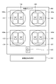
- FIG. 2 is a diagram illustrating a configuration example of pixel groups according to the first embodiment of the present disclosure.
- This figure is a block diagram showing a configuration example of the pixel group 200.
- a pixel group 200 includes a plurality of pixels 100 and a first charge storage portion 230 .
- a pixel group 200 in the figure represents an example including four pixels 100, pixels 100a, 100b, 100c and 100d.
- an image signal generator 220 is arranged for each pixel group 200 .
- a photoelectric conversion unit and a charge transfer unit are arranged in the pixel 100 .
- Photoelectric conversion units 101 and 102 are arranged in a pixel 100a in FIG.
- Photoelectric conversion units 103 and 104 are arranged in a pixel 100b in the figure.
- Photoelectric conversion units 105 and 106 are arranged in a pixel 100c in FIG.
- Photoelectric conversion units 107 and 108 are arranged in a pixel 100d in the figure.
- the photoelectric conversion unit 101 and the like perform photoelectric conversion of incident light. Further, the photoelectric conversion unit 101 and the like hold charges generated by photoelectric conversion.
- the charge transfer unit is arranged for each photoelectric conversion unit 101 and the like, and transfers charges generated and held by the photoelectric conversion unit 101 and the like to the first charge holding unit 230 .
- the charge transfer section can be composed of MOS transistors.
- the pixel 100 is provided with an on-chip lens that collects incident light from a subject.
- a circle drawn in a pixel 100 in the figure represents an on-chip lens.
- a color filter can also be arranged in the pixel 100 .
- This color filter is an optical filter that transmits incident light of a predetermined wavelength out of incident light. Three types of color filters that transmit red light, green light and blue light can be used as this color filter.
- the first charge holding unit 230 holds charges generated by the photoelectric conversion unit 101 and the like.
- the first charge holding portion 230 can be composed of a relatively high impurity concentration semiconductor region formed on the semiconductor substrate on which the pixels 100 are formed. Such a semiconductor region is called a floating diffusion region (FD).
- FD floating diffusion region
- FIG. 3 is a diagram illustrating an example of a circuit configuration of a pixel group according to the first embodiment of the present disclosure; This figure is a circuit diagram showing a configuration example of the pixel group 200 .
- Charge transfer sections 111 and 112, charge transfer sections 113 and 114, charge transfer sections 115 and 116, and charge transfer sections 117 and 118 are arranged in pixels 100a, 100b, 100c and 100d in the figure, respectively.
- These charge transfer units 111 to 118 can be configured by n-channel MOS transistors.
- the image signal generator 220 also includes a reset transistor 221 , an amplification transistor 222 and a selection transistor 223 . These can be composed of n-channel MOS transistors. "RST”, “AMP” and “SEL” in the figure represent a reset transistor, an amplification transistor and a selection transistor, respectively.
- a second charge holding portion 231 and a charge holding portion connecting portion 232 are also shown in the figure.
- the second charge holding unit 231 is connected in parallel to the first charge holding unit 230 and holds charges generated by the photoelectric conversion unit 101 and the like.
- the second charge holding unit 231 can be composed of, for example, a capacitor.
- the charge holding portion connecting portion 232 connects the second charge holding portion 231 to the first charge holding portion 230 .
- the charge holding portion connecting portion 232 can be configured by an n-channel MOS transistor. "FD”, "C” and “FDG” in the figure represent the first charge holding portion, the second charge holding portion and the charge holding portion connecting portion, respectively.
- the signal lines 11 and 12 are wired to the pixel group 200 and the image signal generator 220 .
- Signal lines 11 in FIG. Line FDG is included.
- the signal line 12 also includes a signal line VSL.
- the image signal generator 220 is wired with a power line Vdd.
- the power supply line Vdd is a wiring that supplies power to the image signal generator 220 .
- the signal line 12 is an example of the charge transfer portion signal line described in the claims.
- the signal line VSL is an example of the image signal line described in the claims.
- the anode of photoelectric conversion unit 101 is grounded, and the cathode is connected to the source of charge transfer unit 111 .
- the photoelectric conversion unit 102 has an anode grounded and a cathode connected to the source of the charge transfer unit 112 .
- the photoelectric conversion unit 103 has an anode grounded and a cathode connected to the source of the charge transfer unit 113 .
- the photoelectric conversion unit 104 has an anode grounded and a cathode connected to the source of the charge transfer unit 114 .
- the photoelectric conversion unit 105 has an anode grounded and a cathode connected to the source of the charge transfer unit 115 .
- the anode of photoelectric conversion unit 106 is grounded, and the cathode is connected to the source of charge transfer unit 116 .
- the photoelectric conversion unit 107 has an anode grounded and a cathode connected to the source of the charge transfer unit 117 .
- the anode of photoelectric conversion unit 108 is grounded, and the cathode is connected to the source of charge transfer unit 118 .
- Each drain of the charge transfer portion 111, the charge transfer portion 112, the charge transfer portion 113, the charge transfer portion 114, the charge transfer portion 115, the charge transfer portion 116, the charge transfer portion 117, and the charge transfer portion 118 is connected to the first charge holding portion. It is commonly connected to one end of the portion 230 . Further, the gate of the amplification transistor 222, the source of the reset transistor 221, and the drain of the charge holding section connection section 232 are further connected to one end of the first charge holding section 230. FIG. Another end of the first charge holding unit 230 is grounded. The drain of the reset transistor 221 and the drain of the amplification transistor 222 are connected to the power supply line Vdd. The source of the amplification transistor 222 is connected to the drain of the selection transistor 223, and the source of the selection transistor 223 is connected to the signal line VSL.
- a gate of the charge transfer unit 111 is connected to the signal line TRG0.
- a gate of the charge transfer unit 112 is connected to the signal line TRG1.
- a gate of the charge transfer unit 113 is connected to the signal line TRG2.
- a gate of the charge transfer unit 114 is connected to the signal line TRG3.
- a gate of the charge transfer unit 115 is connected to the signal line TRG4.
- a gate of the charge transfer unit 116 is connected to the signal line TRG5.
- a gate of the charge transfer unit 117 is connected to the signal line TRG6.
- a gate of the charge transfer unit 118 is connected to the signal line TRG7.
- a gate of the reset transistor 221 is connected to the signal line RST.
- a gate of the charge holding unit connection unit 232 is connected to the signal line FDG.
- One end of the second charge holding portion 231 is grounded, and the other end is connected to the source of the charge holding portion connecting portion 232 .
- the other end of the second charge holding portion 231 is further connected to the source of the second charge holding portion 232 ′ of the adjacent pixel group 200 .
- the reset transistor 221 resets the first charge holding section 230 . This reset can be performed by conducting between the first charge holding portion 230 and the power supply line Vdd to discharge the charge of the first charge holding portion 230 . A control signal for the reset transistor 221 is transmitted through a signal line RST.
- the amplification transistor 222 amplifies the voltage of the first charge holding section 230 .
- a gate of the amplification transistor 222 is connected to the first charge holding unit 230 . Therefore, an image signal is generated at the source of the amplification transistor 222 with a voltage corresponding to the charge held in the first charge holding unit 230 .
- the selection transistor 223 By turning on the selection transistor 223, the image signal can be output to the signal line VO.
- a control signal for the select transistor 223 is transmitted by a signal line SEL.
- the charge transfer units 111-118, the reset transistor 221, the selection transistor 223, and the charge holding unit connection unit 232 can be configured by n-channel MOS transistors.
- the drain-source can be made conductive by applying a voltage exceeding the threshold of the gate-source voltage Vgs to the gate.
- a voltage exceeding the threshold of the gate-source voltage Vgs is hereinafter referred to as an on-voltage.
- a control signal including this on-voltage is transmitted by a signal line TRG0 or the like.
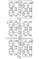
- FIG. 4 is a diagram illustrating an arrangement example of pixel groups according to the first embodiment of the present disclosure.
- This figure is a diagram showing an arrangement example of the pixel group 200 and the image signal generator 220 .
- the figure also shows a plurality of pixel groups 200 arranged in a two-dimensional matrix in the pixel array unit 10.
- the arrangement of the pixel groups 200 in the horizontal direction (x direction) in the figure represents a row.
- the arrangement of pixel groups 200 in the vertical direction (y direction) represents a column.
- This figure shows an example of a plurality of pixel groups 200 arranged in two rows and three columns.
- the pixel group 200 and the image signal generator 220 shown in FIG. 3 are shown in a simplified form.
- the signal lines 11 (not shown) arranged for each row are wired extending in the row direction (horizontal direction) and the pixel groups 200 arranged in the same row. are wired in common to On the other hand, the signal lines VSL can be wired in the column direction (vertical direction).
- An image signal generating section 220a, a first charge holding section 230a, and a charge holding section connection section 232a are arranged adjacent to the pixel group 200a in the middle of the upper row in the figure on the lower side of the drawing.
- an image signal generation section 220b, a first charge holding section 230b, and a charge holding section connection section 232b are arranged adjacent to each other on the upper side of the figure. .
- the image signal generation section 220c, the first charge holding section 230c, and the charge holding section connecting section 232c are arranged adjacent to each other on the upper side of the figure. .
- the image signal generator 220a and the image signal generator 220b are connected to the same signal line VSL and commonly output the generated image signal.
- Pixel groups 200a and pixel groups 200b corresponding to the image signal generators 220a and 220b, respectively, are arranged in adjacent rows. That is, pixel group 200a and pixel group 200b are arranged in different rows. Accordingly, the pixel group 200a and the image signal generation unit 220a and the pixel group 200b and the image signal generation unit 220b can generate image signals at different timings.
- the image signal generating section 220a and the image signal generating section 220c are connected to the same second charge holding section 231 via the charge holding section connection section 232a and the charge holding section connection section 232c, respectively.
- 231 is shared.
- Pixel groups 200a and pixel groups 200c corresponding to the image signal generators 220a and 220c, respectively, are arranged in adjacent rows. Accordingly, the pixel group 200a and the pixel group 200c can connect the second charge holding portion 231 to their own first charge holding portion 230 at different timings.
- the signal line VSL is shared between the image signal generators 220a and 220b corresponding to the pixel groups 200a and 200b arranged in different rows.
- the pixel group 200a and the pixel group 200c arranged in different rows share the second charge holding unit 231.
- the signal line 11 can be commonly wired to the pixel groups 200 arranged in the same row, and the same control signal can be simultaneously transmitted to the pixel groups 200 arranged in the same row.
- the pixel group 200a and the pixel group 200b are arranged in adjacent rows and adjacent columns. Therefore, the image signal generators 220a and 220b arranged in the pixel group 200a and the pixel group 200b can be arranged adjacent to each other.
- the selection transistors 223 of the image signal generation unit 220a and the image signal generation unit 220b can be arranged close to each other and arranged at positions facing each other with the signal line VSL interposed therebetween. Thereby, the wiring between the image signal generator 220a and the image signal generator 220b and the signal line VSL can be shortened.
- the pixel group 200a and the pixel group 200c are also arranged in adjacent rows and adjacent columns. It is possible to arrange the charge holding portion connecting portion 232a and the charge holding portion connecting portion 232c close to each other and to face each other with the second charge holding portion 231 interposed therebetween. Accordingly, wiring between the pixel groups 200a and 200c and the second charge holding portion 231 via the charge holding portion connecting portion 232 can be shortened. Thereby, the wiring configuration of the pixel array section 10 can be simplified.
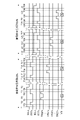
- FIG. 5 is a diagram illustrating an example of image signal generation according to an embodiment of the present disclosure.
- This figure is a timing chart showing an example of image signal generation in the pixel group 200 and the image signal generator 220 . Also, this figure shows the generation of the image signal by the image signal generator 220b and the image signal generator 220b in FIG.
- "SEL", “RST”, “TRG0” and “TRG7” in the figure represent signals on the signal line SEL, the signal line RST, the signal line TRG0 and the signal line TRG7, respectively.
- “a” and “b” are symbols indicating control signals for the rows of the image signal generator 220a and the image signal generator 220b.
- VSL represents an image signal output to the signal line VSL.
- this figure shows an example in which 0 V is applied as the voltage for turning off the MOS transistor to be controlled in the control signal.
- a configuration in which another voltage is applied as the voltage (off voltage) for turning off the MOS transistor can also be adopted.
- a negative voltage such as -1.2 V can be applied as an off-voltage to the signal line SEL and the signal line TRG (signal line TRG0a, etc.).
- the first half (T1 to T18) of the figure represents the generation of image signals in the image signal generator 220a and the pixel group 200a
- the latter half (T19 to T36) represents the generation of image signals in the image signal generator 220b and the pixel group 200b.
- 0V is applied to the signal line SELa, the signal line RSTa, the signal line SELb, the signal line RSTb, the signal line TRG0a, the signal line TRG7a, the signal line TRG0b, and the signal line TRG7b.
- an ON voltage is applied to the signal line SELa.
- Application of the ON voltage to the signal line SELa continues until T9.
- an ON voltage is applied to the signal line RSTa. This resets the first charge holding unit 230 .
- the application of the ON voltage to the signal line RSTa is stopped.
- an ON voltage is applied to the signal line TRG0a.
- the charge transfer unit 111 of the pixel group 200a becomes conductive, and the charge of the photoelectric conversion unit 101 is transferred to the first charge holding unit 230 and held.
- the exposure period in the photoelectric conversion unit 101 ends at T4.
- the image signal generation unit 220a generates an image signal “0a” based on the charges held in the first charge holding unit 230, and outputs the image signal “0a” to the signal line VSL until the next period T6.
- an ON signal is applied to the signal line RSTa and the signal line TRG0a, and the reset transistor 221 and the charge transfer section 111 become conductive. Thereby, the first charge holding unit 230 and the photoelectric conversion unit 101 are reset. The application of the ON voltage to the signal line RSTa continues until T8.
- the application of the ON voltage to the signal line TRG0a is stopped.
- the application of the ON voltage to the signal line RSTa is stopped. Thereby, the exposure period of the next cycle in the photoelectric conversion unit 101 is started.
- the application of the ON voltage to the signal line SELa is stopped.
- the signal lines TRG1a to TRG6a are reset and image signals are generated in the same manner as T1 to T9.
- an ON voltage is applied to the signal line SELa.
- the application of the ON voltage to the signal line SELa continues until T18.
- an ON voltage is applied to the signal line RSTa, and the first charge holding unit 230 is reset.
- the application of the ON voltage to the signal line RSTa is stopped.
- an ON voltage is applied to the signal line TRG7a.
- the charge transfer unit 118 of the pixel group 200a becomes conductive, and the charge of the photoelectric conversion unit 108 is transferred to and held in the first charge holding unit 230.
- FIG. The exposure period in the photoelectric conversion unit 108 ends at T13.
- the image signal generation unit 220a generates the image signal “7a” based on the charges held in the first charge holding unit 230, and outputs the image signal “7a” to the signal line VSL until the next T15.
- an ON signal is applied to the signal line RSTa and the signal line TRG7a, and the reset transistor 221 and the charge transfer section 118 become conductive. Thereby, the first charge holding unit 230 and the photoelectric conversion unit 108 are reset. The application of the ON voltage to the signal line RSTa continues until T17.
- the application of the ON voltage to the signal line TRG7a is stopped.
- the application of the ON voltage to the signal line RSTa is stopped.
- the exposure period of the next cycle in the photoelectric conversion unit 108 is started.
- the application of the ON voltage to the signal line SELa is stopped.
- An image signal can be generated in the image signal generation unit 220a by the procedures from T1 to T18 described above.
- an ON voltage is applied to the signal line SELb.
- Application of the ON voltage to the signal line SELb continues until T27.
- an ON voltage is applied to the signal line RSTb, and the first charge holding unit 230 is reset.
- the application of the ON voltage to the signal line RSTb is stopped.
- an ON voltage is applied to the signal line TRG0b.
- the charge transfer unit 111 becomes conductive, and the charge in the photoelectric conversion unit 101 is transferred to and held in the first charge holding unit 230 .
- the exposure period in the photoelectric conversion unit 101 at T22 ends.
- the image signal generation unit 220b generates the image signal “0b” based on the charges held in the first charge holding unit 230, and outputs the image signal “0b” to the signal line VSL until the next T24.
- an ON signal is applied to the signal line RSTb and the signal line TRG0b, and the reset transistor 221 and the charge transfer section 111 become conductive. Thereby, the first charge holding unit 230 and the photoelectric conversion unit 101 are reset. The application of the ON voltage to the signal line RSTa continues until T26.
- the signal lines TRG1b to TRG6b are reset and image signals are generated in the same manner as T19 to T27.
- an ON voltage is applied to the signal line SELb.
- Application of the ON voltage to the signal line SELb continues until T36.
- an ON voltage is applied to the signal line RSTb, and the first charge holding unit 230 is reset.
- the application of the ON voltage to the signal line RSTb is stopped.
- an ON voltage is applied to the signal line TRG7b.
- the charge transfer unit 118 of the pixel group 200b becomes conductive, and the charge of the photoelectric conversion unit 108 is transferred to the first charge holding unit 230 and held.
- the exposure period in the photoelectric conversion unit 108 ends at T31.
- the image signal generation unit 220b generates the image signal “7b” based on the charges held in the first charge holding unit 230, and outputs the image signal “7b” to the signal line VSL until the next T33.
- an ON signal is applied to the signal line RSTb and the signal line TRG7b, and the reset transistor 221 and the charge transfer section 118 become conductive. Thereby, the first charge holding unit 230 and the photoelectric conversion unit 108 are reset. The application of the ON voltage to the signal line RSTb continues until T35.
- An image signal can be generated in the image signal generator 220b according to the procedure from T28 to T32 described above.
- the procedure for generating the image signal in the image signal generation unit 220 is not limited to this example.
- resetting of the first charge holding unit 230 after generation of the image signal can be omitted.
- the reset processing from T6 to T8 in FIG. 5 can be omitted.
- the output of the image signal (“0a” in FIG. 6) to the signal line VSL is continued until the next reset (T11) of the first charge holding unit 230 .
- FIG. 6 and 7 are diagrams showing other examples of pixel group arrangement according to the first embodiment of the present disclosure. 6 and 7 are diagrams showing examples of arrangement of the pixel group 200 and the image signal generator 220, similar to FIG.
- the image signal generator 220a is divided into portions each having a selection transistor 223, an amplification transistor 222, and a reset transistor 221, which are arranged above and below the pixel group 200a, respectively.
- portions including the selection transistor 223, the amplification transistor 222, and the reset transistor 221 are arranged below and above the pixel group 200a, respectively.
- portions each including the selection transistor 223, the amplification transistor 222, and the reset transistor 221 are arranged below and above the pixel group 200a.
- Signal lines 11 (not shown) are wired extending in the row direction (horizontal direction).
- the signal lines VSL can be wired in the column direction (vertical direction).
- the pixel group 200a and the pixel group 200b are arranged in adjacent rows.
- the image signal generator 220a and the image signal generator 220b are commonly connected to the signal line VSL.
- the image signal generator 220 a and the pixel group 200 c are arranged in adjacent rows and columns, and the image signal generator 220 a and the image signal generator 220 c share the second charge holding unit 231 .
- the pixel group 200a and the image signal generation section 220a in the figure are configured in a shape obtained by rotating the pixel group 200a and the image signal generation section 220a in FIG. 4 by 90 degrees.
- the pixel group 200a, the pixel group 200b, and the pixel group 200c are arranged in different rows. Also, the pixel group 200a, the pixel group 200b, and the pixel group 200c are arranged in the same column.
- signal lines 11 (not shown) are wired extending in the row direction (horizontal direction). Also, the signal lines VSL can be wired in the column direction (vertical direction).
- the pixel group 200a and the pixel group 200b are arranged in adjacent rows, and the image signal generator 220a and the image signal generator 220b are commonly connected to the signal line VSL.
- the image signal generator 220 a and the pixel group 200 c are arranged in adjacent rows, and the image signal generator 220 a and the image signal generator 220 c share the second charge holding unit 231 .
- the imaging device 1 connects the second charge holding unit 231 to each pixel of the pixel group 200 to adjust the dynamic range. Therefore, it is possible to prevent a decrease in resolution. Further, by arranging the two pixel groups 200 sharing the signal line VSL for outputting the image signal in different rows, the two pixel groups 200 can be driven at different timings. A control signal line can be wired in common to the pixel groups 200 arranged in the same row, and the configuration of the pixel array section 10 can be simplified.
- the imaging device 1 of the first embodiment described above uses the second charge holding unit 231 .
- the imaging device 1 of the second embodiment of the present disclosure differs from the above-described first embodiment in that the second charge holding unit 231 is omitted.
- FIG. 8 is a diagram illustrating a configuration example of an imaging device according to the second embodiment of the present disclosure. This figure, like FIG. 1, is a block diagram showing a configuration example of the imaging element 1. As shown in FIG. The imaging device 1 in FIG. 8 differs from the imaging device 1 in FIG. 1 in that the second charge holding unit 231 is omitted.
- FIG. 8 is a diagram illustrating an example of a circuit configuration of a pixel group according to the second embodiment of the present disclosure.
- This figure, like FIG. 3, is a circuit diagram showing a configuration example of the pixel group 200.
- the pixel group 200 in FIG. 3 differs from the pixel group 200 in FIG. 3 in that the second charge holding portion 231 is omitted.
- the drain of the charge holding portion connecting portion 232 is directly connected to the first charge holding portion 230 of the adjacent pixel group 200 .
- the first charge holding portion 230 of the adjacent pixel group 200 is used as the second charge holding portion 231 .
- FIG. 9 is a diagram illustrating an arrangement example of pixel groups according to the second embodiment of the present disclosure.
- This figure like FIG. 4, is a diagram showing an arrangement example of the pixel group 200 and the image signal generator 220. In FIG. It differs from the pixel group 200 in FIG. 4 in that the second charge holding portion 231 is omitted.
- the image signal generation unit 220a and the image signal generation unit 220c in the figure share the charge holding unit connection unit 232a.
- the configuration of the imaging device 1 other than this is the same as the configuration of the imaging device 1 in the first embodiment of the present disclosure, the description is omitted.
- the imaging device 1 of the second embodiment of the present disclosure can simplify the configuration of the pixel array section 10 by omitting the second charge holding section 231 .
- the imaging device 1 of the first embodiment described above a plurality of photoelectric conversion units are arranged in the pixels 100 .
- the imaging device 1 of the third embodiment of the present disclosure differs from the first embodiment described above in that one photoelectric conversion unit is arranged in the pixel 100 .
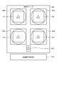
- FIG. 10 is a diagram illustrating a configuration example of pixel groups according to the third embodiment of the present disclosure.
- This figure like FIG. 2, is a block diagram showing a configuration example of a pixel group 200.
- a pixel 100a shown in FIG. A pixel 100 b in FIG. 1 includes a photoelectric conversion unit 103 .
- a pixel 100 c in the figure includes a photoelectric conversion unit 105 .
- one photoelectric conversion unit 101 or the like is arranged in the pixel 100 in FIG.
- a pixel group 200 in the figure generates a normal image signal.
- FIG. 11 is a diagram illustrating an example of a circuit configuration of a pixel group according to the third embodiment of the present disclosure; This figure, like FIG. 3, is a circuit diagram showing a configuration example of the pixel group 200. As shown in FIG. The pixel group 200 in FIG. 3 differs from the pixel group 200 in FIG. 3 in that the photoelectric conversion units 102, 104, 106 and 108 and the charge transfer units 112, 114, 116 and 118 are omitted.
- two pixel groups 200 sharing the signal line VSL for outputting image signals can be arranged in different rows.
- the configuration of the imaging device 1 other than this is the same as the configuration of the imaging device 1 in the first embodiment of the present disclosure, the description is omitted.
- the two pixel groups 200 that share the signal line VSL that outputs the image signals are arranged in different rows. Deploy. As a result, these two pixel groups 200 can be driven at different timings, and control signal lines can be commonly wired to the pixel groups 200 arranged in the same row.
- the technology according to the present disclosure can be applied to various products.
- the technology according to the present disclosure can be applied to imaging devices such as cameras.
- FIG. 12 is a diagram showing a configuration example of an imaging device to which the technology according to the present disclosure can be applied.
- An imaging apparatus 1000 shown in FIG. 12 is a diagram showing a configuration example of an imaging device to which the technology according to the present disclosure can be applied.
- a photographing lens 1006 is a lens that collects light from a subject.
- the photographing lens 1006 forms an image of the subject on the light receiving surface of the image sensor 1001 .
- An imaging device 1001 is a device that takes an image of a subject.
- a plurality of pixels each having a photoelectric conversion unit for performing photoelectric conversion of light from an object are arranged on the light receiving surface of the image sensor 1001 . These pixels each generate an image signal based on charges generated by photoelectric conversion.
- the image sensor 1001 converts image signals generated by pixels into digital image signals and outputs the digital image signals to the image processing unit 1003 .
- An image signal for one screen is called a frame.
- the imaging device 1001 can also output an image signal on a frame-by-frame basis.
- the control unit 1002 controls the image pickup device 1001 and the image processing unit 1003 .
- the control unit 1002 can be configured by an electronic circuit using a microcomputer or the like, for example.
- the image processing unit 1003 processes the image signal from the imaging device 1001 .
- the image signal processing in the image processing unit 1003 corresponds to, for example, demosaic processing for generating image signals of insufficient colors when generating a color image, and noise reduction processing for removing noise from image signals.
- the image processing unit 1003 can be configured by, for example, an electronic circuit using a microcomputer or the like.
- the display unit 1004 displays an image based on the image signal processed by the image processing unit 1003 .
- the display unit 1004 can be configured by, for example, a liquid crystal monitor.
- a recording unit 1005 records an image (frame) based on the image signal processed by the image processing unit 1003 .
- the recording unit 1005 can be composed of, for example, a hard disk or a semiconductor memory.
- the imaging device to which the present disclosure can be applied has been described above.
- the present technology can be applied to the imaging device 1001 among the above components.
- the image sensor 1 described with reference to FIG. 1 can be applied to the image sensor 1001 .
- the image processing unit 1003 is an example of a processing circuit described in claims.
- the imaging device 1000 is an example of the imaging device described in the claims.
- a plurality of charge transfer unit signals arranged for each row in the two-dimensional matrix, transmitting control signals of the charge transfer units of the pixel groups, respectively, and commonly connected to the plurality of pixel groups arranged in the row.
- an image signal line for commonly outputting the image signals generated by the image signal generators respectively arranged in the pixel groups arranged in adjacent rows in the two-dimensional matrix; and a second charge storage unit commonly connected to the charge storage units of the pixel groups arranged in adjacent rows in the two-dimensional matrix.
- a pixel array unit in which the groups are arranged in a two-dimensional matrix; an image signal generating unit arranged for each pixel group and generating an image signal based on the held charges; A plurality of charge transfer unit signals arranged for each row in the two-dimensional matrix, transmitting control signals of the charge transfer units of the pixel groups, respectively, and commonly connected to the plurality of pixel groups arranged in the row. Lines and, an image signal line for commonly outputting the image signals generated by the image signal generators respectively arranged in the pixel groups arranged in adjacent rows in the two-dimensional matrix; a second charge storage unit commonly connected to the charge storage units of the pixel groups arranged in adjacent rows in the two-dimensional matrix; and a processing circuit for processing the output image signal.
- Reference Signs List 1 1001 image sensor 12 signal line 10 pixel array section 30 column signal processing section 100 pixels 100a, 100b, 100c, 100d pixels 101 to 108 photoelectric conversion sections 111 to 118 charge transfer sections 200, 200a, 200b, 200c pixel group 220, 220a, 220b, 220c image signal generating section 230, 230a, 230b, 230c first charge holding section 231 second charge holding section 232, 232a, 232b, 232c charge holding section connection section 1000 imaging device 1003 image processing section
Landscapes
- Engineering & Computer Science (AREA)
- Multimedia (AREA)
- Signal Processing (AREA)
- Solid State Image Pick-Up Elements (AREA)
- Transforming Light Signals Into Electric Signals (AREA)
Abstract
画素毎にダイナミックレンジを調整する。画素アレイ部は、光電変換部及び光電変換部により生成される電荷を転送する電荷転送部を備える複数の画素と電荷転送部により転送される電荷を保持する第1の電荷保持部とをそれぞれ有する複数の画素グループが2次元行列に配置される。画像信号生成部は、画素グループ毎に配置されて保持された電荷に基づいて画像信号を生成する。複数の電荷転送部信号線は、2次元行列における行毎に配置されて画素グループの電荷転送部の制御信号をそれぞれ伝達するとともに行に配置される複数の画素グループに共通に接続される。画像信号線は、2次元行列における隣接する行に配置される画素グループにそれぞれ配置される画像信号生成部により生成される画像信号が共通に出力される。第2の電荷保持部は、2次元行列における隣接する行に配置される画素グループの電荷保持部に共通に接続される。
Description
本開示は、撮像素子及び撮像装置に関する。
撮像レンズの焦点位置を検出してオートフォーカスを行う撮像素子では、被写体像の像面位相差を検出するための位相差信号を生成する画素が配置される。この画素のうち複数の光電変換部が1つの画素に配置される画素は、複数の光電変換部の光電変換によりそれぞれ生成される電荷に基づいて複数の画像信号を生成する。この光電変換部毎の画像信号が位相差信号として使用される。また、この画素においては、複数の光電変換部により生成される電荷を加算した電荷に基づく画像信号を出力することもできる。この加算した電荷に基づく画像信号は、被写体の画像を表す画像信号として使用することができる。このような画素が受光面の全面に配置された撮像素子が使用されている。
例えば、同色のカラーフィルタ及び複数の画素を備える画素セット毎に画像信号を生成する撮像素子が提案されている(例えば、特許文献1参照)。この撮像素子では、画素セットに含まれる複数の光電変換部に対して画像信号の生成に使用する光電変換部の個数を調整することによりダイナミックレンジを調整する。
しかしながら、上記の従来技術では、画素セット単位にてダイナミックレンジの調整を行うため、解像度が低下するという問題がある。
そこで、本開示では、画素毎にダイナミックレンジを調整する撮像素子及び撮像装置を提案する。
本開示の撮像素子は、画素アレイ部と、画像信号生成部と、複数の電荷転送部信号線と、画像信号線と、第2の電荷保持部とを有する。画素アレイ部は、光電変換部及び上記光電変換部により生成される電荷を転送する電荷転送部を備える複数の画素と上記電荷転送部により転送される電荷を保持する第1の電荷保持部とをそれぞれ有する複数の画素グループが2次元行列に配置される。画像信号生成部は、上記画素グループ毎に配置されて上記保持された電荷に基づいて画像信号を生成する。複数の電荷転送部信号線は、上記2次元行列における行毎に配置されて上記画素グループの上記電荷転送部の制御信号をそれぞれ伝達するとともに上記行に配置される複数の上記画素グループに共通に接続される。画像信号線は、上記2次元行列における隣接する行に配置される上記画素グループにそれぞれ配置される上記画像信号生成部により生成される上記画像信号が共通に出力される。第2の電荷保持部は、上記2次元行列における隣接する行に配置される上記画素グループの上記第1の電荷保持部に共通に接続される。
以下に、本開示の実施形態について図面に基づいて詳細に説明する。説明は、以下の順に行う。なお、以下の各実施形態において、同一の部位には同一の符号を付することにより重複する説明を省略する。
1.第1の実施形態
2.第2の実施形態
3.第3の実施形態
4.撮像装置の構成
1.第1の実施形態
2.第2の実施形態
3.第3の実施形態
4.撮像装置の構成
(1.第1の実施形態)
[撮像素子の構成]
図1は、本開示の実施形態に係る撮像素子の構成例を示す図である。同図は、撮像素子1の構成例を表すブロック図である。この撮像素子1を例に挙げて本開示の実施形態に係る半導体素子を説明する。撮像素子1は、被写体の画像データを生成する半導体素子である。撮像素子1は、画素アレイ部10と、垂直駆動部20と、カラム信号処理部30と、制御部40とを備える。
[撮像素子の構成]
図1は、本開示の実施形態に係る撮像素子の構成例を示す図である。同図は、撮像素子1の構成例を表すブロック図である。この撮像素子1を例に挙げて本開示の実施形態に係る半導体素子を説明する。撮像素子1は、被写体の画像データを生成する半導体素子である。撮像素子1は、画素アレイ部10と、垂直駆動部20と、カラム信号処理部30と、制御部40とを備える。
画素アレイ部10は、複数の画素グループ200が配置されて構成されたものである。この画素アレイ部10は、複数の画素グループ200が2次元行列の形状に配置される。ここで、画素グループ200は、入射光の光電変換を行う光電変換部を有する複数の画素と光電変換により生成される電荷を保持する電荷保持部(後述する第1の電荷保持部230)とを備えて構成されるものである。また、画素グループ200毎に画像信号生成部(後述する画像信号生成部220)が配置される。この画像信号生成部220は、画素グループ200の第1の電荷保持部230に保持された電荷に基づいて画像信号を生成する。その光電変換部には、例えば、フォトダイオードを使用することができる。
それぞれの画素グループ200及び画像信号生成部220には、信号線11が配線される。画素グループ200及び画像信号生成部220は、信号線11により伝達される制御信号により制御される。また、画像信号生成部220には、信号線12が配線される。この信号線12には、画像信号生成部220から画像信号が出力される。なお、信号線11は、2次元行列の形状の行毎に配置され、1行に配置された複数の画素グループ200及び画像信号生成部220に共通に配線される。信号線12は、2次元行列の列方向に配置される。
垂直駆動部20は、上述の画素グループ200の制御信号を生成するものである。同図の垂直駆動部20は、画素アレイ部10の2次元行列の行毎に制御信号を生成し、信号線11を介して順次出力する。
カラム信号処理部30は、画素グループ200により生成された画像信号の処理を行うものである。同図のカラム信号処理部30は、信号線12を介して伝達される画素アレイ部10の1行に配置された複数の画素グループ200からの画像信号の処理を同時に行う。この処理として、例えば、画素グループ200により生成されたアナログの画像信号をデジタルの画像信号に変換するアナログデジタル変換や画像信号のオフセット誤差を除去する相関二重サンプリング(CDS:Correlated Double Sampling)を行うことができる。処理後の画像信号は、撮像素子1の外部の回路等に対して出力される。
制御部40は、垂直駆動部20及びカラム信号処理部30を制御するものである。同図の制御部40は、信号線41及び42を介して制御信号をそれぞれ出力して垂直駆動部20及びカラム信号処理部30を制御する。なお、同図の撮像素子1は、請求の範囲に記載の半導体素子の一例である。カラム信号処理部30は、請求の範囲に記載の処理回路の一例である。
[画素グループの構成]
図2は、本開示の第1の実施形態に係る画素グループの構成例を示す図である。同図は、画素グループ200の構成例を表すブロック図である。画素グループ200は、複数の画素100と、第1の電荷保持部230とを備える。同図の画素グループ200は、画素100a、100b、100c及び100dの4つの画素100を備える例を表したものである。また、画素グループ200毎に画像信号生成部220が配置される。
図2は、本開示の第1の実施形態に係る画素グループの構成例を示す図である。同図は、画素グループ200の構成例を表すブロック図である。画素グループ200は、複数の画素100と、第1の電荷保持部230とを備える。同図の画素グループ200は、画素100a、100b、100c及び100dの4つの画素100を備える例を表したものである。また、画素グループ200毎に画像信号生成部220が配置される。
画素100には、光電変換部と、電荷転送部(不図示)とが配置される。同図の画素100aには、光電変換部101及び102が配置される。同図の画素100bには、光電変換部103及び104が配置される。同図の画素100cには、光電変換部105及び106が配置される。同図の画素100dには、光電変換部107及び108が配置される。前述のように光電変換部101等は、入射光の光電変換を行う。また、光電変換部101等は、光電変換により生成した電荷を保持する。
電荷転送部は、光電変換部101等毎に配置され、光電変換部101等により生成されて保持された電荷を第1の電荷保持部230に転送するものである。後述するように、電荷転送部は、MOSトランジスタにより構成することができる。
また、画素100には、被写体からの入射光を集光するオンチップレンズが配置される。同図の画素100に記載した円は、オンチップレンズを表す。なお、画素100には、カラーフィルタを配置することもできる。このカラーフィルタは、入射光のうちの所定の波長の入射光を透過する光学的なフィルタである。このカラーフィルタとして赤色光、緑色光及び青色光を透過する3種類のカラーフィルタを使用することができる。
第1の電荷保持部230は、光電変換部101等により生成される電荷を保持するものである。この第1の電荷保持部230は、画素100が形成される半導体基板に形成される比較的高い不純物濃度の半導体領域により構成することができる。このような半導体領域は、浮遊拡散領域(FD:Floating Diffusion)と称される。
[画素グループの回路構成]
図3は、本開示の第1の実施形態に係る画素グループの回路構成の一例を示す図である。同図は、画素グループ200の構成例を表す回路図である。同図の画素100a、100b、100c及び100dには、それぞれ電荷転送部111及び112、電荷転送部113及び114、電荷転送部115及び116並びに電荷転送部117及び118が配置される。これら電荷転送部111-118は、nチャネルMOSトランジスタにより構成することができる。
図3は、本開示の第1の実施形態に係る画素グループの回路構成の一例を示す図である。同図は、画素グループ200の構成例を表す回路図である。同図の画素100a、100b、100c及び100dには、それぞれ電荷転送部111及び112、電荷転送部113及び114、電荷転送部115及び116並びに電荷転送部117及び118が配置される。これら電荷転送部111-118は、nチャネルMOSトランジスタにより構成することができる。
また、画像信号生成部220は、リセットトランジスタ221、増幅トランジスタ222及び選択トランジスタ223を備える。これらは、nチャネルMOSトランジスタにより構成することができる。同図の「RST」、「AMP」及び「SEL」は、それぞれリセットトランジスタ、増幅トランジスタ及び選択トランジスタを表す。
また、同図には、第2の電荷保持部231と電荷保持部接続部232を更に記載した。第2の電荷保持部231は、第1の電荷保持部230に並列に接続されて光電変換部101等により生成される電荷を保持するものである。第2の電荷保持部231は、例えば、キャパシタにより構成することができる。第2の電荷保持部231を接続することにより第1の電荷保持部230の電荷保持容量を増加させることができる。これにより、画素グループ200の電荷保持部の電荷保持容量を変更することができ、ダイナミックレンジを調整することができる。電荷保持部接続部232は、第2の電荷保持部231を第1の電荷保持部230に接続するものである。電荷保持部接続部232は、nチャネルMOSトランジスタにより構成することができる。同図の「FD」、「C」及び「FDG」は、それぞれ第1の電荷保持部、第2の電荷保持部及び電荷保持部接続部を表す。
前述のように、画素グループ200及び画像信号生成部220には、信号線11及び12が配線される。同図の信号線11には、信号線TRG0、信号線TRG1、信号線TRG2、信号線TRG3、信号線TRG4、信号線TRG5、信号線TRG6、信号線TRG7、信号線RST、信号線SEL及び信号線FDGが含まれる。また、信号線12には、信号線VSLが含まれる。この他、画像信号生成部220は、電源線Vddが配線される。この電源線Vddは、画像信号生成部220に電源を供給する配線である。なお、信号線12は、請求の範囲に記載の電荷転送部信号線の一例である。信号線VSLは、請求の範囲に記載の画像信号線の一例である。
光電変換部101のアノードは接地され、カソードは電荷転送部111のソースに接続される。光電変換部102のアノードは接地され、カソードは電荷転送部112のソースに接続される。光電変換部103のアノードは接地され、カソードは電荷転送部113のソースに接続される。光電変換部104のアノードは接地され、カソードは電荷転送部114のソースに接続される。光電変換部105のアノードは接地され、カソードは電荷転送部115のソースに接続される。光電変換部106のアノードは接地され、カソードは電荷転送部116のソースに接続される。光電変換部107のアノードは接地され、カソードは電荷転送部117のソースに接続される。光電変換部108のアノードは接地され、カソードは電荷転送部118のソースに接続される。
電荷転送部111、電荷転送部112、電荷転送部113、電荷転送部114、電荷転送部115、電荷転送部116、電荷転送部117及び電荷転送部118のそれぞれのドレインは、第1の電荷保持部230の一端に共通に接続される。また、この第1の電荷保持部230の一端には、増幅トランジスタ222のゲート、リセットトランジスタ221のソース及び電荷保持部接続部232のドレインが更に接続される。第1の電荷保持部230の他の一端は、接地される。リセットトランジスタ221のドレイン及び増幅トランジスタ222のドレインは、電源線Vddに接続される。増幅トランジスタ222のソースは選択トランジスタ223のドレインに接続され、選択トランジスタ223のソースは信号線VSLに接続される。
電荷転送部111のゲートは、信号線TRG0に接続される。電荷転送部112のゲートは、信号線TRG1に接続される。電荷転送部113のゲートは、信号線TRG2に接続される。電荷転送部114のゲートは、信号線TRG3に接続される。電荷転送部115のゲートは、信号線TRG4に接続される。電荷転送部116のゲートは、信号線TRG5に接続される。電荷転送部117のゲートは、信号線TRG6に接続される。電荷転送部118のゲートは、信号線TRG7に接続される。リセットトランジスタ221のゲートは信号線RSTに接続される。電荷保持部接続部232のゲートは、信号線FDGに接続される。第2の電荷保持部231の一端は接地され、他の一端は電荷保持部接続部232のソースに接続される。なお、この第2の電荷保持部231の他の一端は、隣接する画素グループ200の第2の電荷保持部232’のソースに更に接続される。
リセットトランジスタ221は、第1の電荷保持部230をリセットするものである。このリセットは、第1の電荷保持部230と電源線Vddとの間を導通して第1の電荷保持部230の電荷を排出することにより行うことができる。リセットトランジスタ221の制御信号は、信号線RSTにより伝達される。
増幅トランジスタ222は、第1の電荷保持部230の電圧を増幅するものである。増幅トランジスタ222のゲートは、第1の電荷保持部230に接続されている。このため、増幅トランジスタ222のソースには、第1の電荷保持部230に保持された電荷に応じた電圧の画像信号が生成される。また、選択トランジスタ223を導通させることにより、この画像信号を信号線VOに出力させることができる。選択トランジスタ223の制御信号は、信号線SELにより伝達される。
前述のように、電荷転送部111-118、リセットトランジスタ221、選択トランジスタ223及び電荷保持部接続部232は、nチャネルMOSトランジスタにより構成することができる。このnチャネルMOSトランジスタでは、ゲート-ソース間電圧Vgsの閾値を超える電圧をゲートに印加することにより、ドレイン-ソース間を導通させることができる。以下、このゲート-ソース間電圧Vgsの閾値を超える電圧をオン電圧と称する。このオン電圧を含む制御信号は、信号線TRG0等により伝達される。
[画素グループの配置]
図4は、本開示の第1の実施形態に係る画素グループの配置例を示す図である。同図は、画素グループ200及び画像信号生成部220の配置例を表す図である。また、同図は、画素アレイ部10において2次元行列に配置される複数の画素グループ200を表したものであり、同図の横方向(x方向)の画素グループ200の並びが行を表し、縦方向(y方向)の画素グループ200の並びが列を表す。同図は、2行3列に配置される複数の画素グループ200の例を表したものである。同図においては、図3に記載した画素グループ200や画像信号生成部220を簡略化して記載した。同図の「RST」、「AMP」、「SEL」、「C」及び「FDG」は、図3と同様にリセットトランジスタ等を表す。なお、図1において説明したように、行毎に配置される信号線11(不図示)は、行の方向(横方向)に伸長して配線されるとともに同一の行に配置される画素グループ200に共通に配線される。一方、信号線VSLは、列の方向(縦方向)に配線することができる。
図4は、本開示の第1の実施形態に係る画素グループの配置例を示す図である。同図は、画素グループ200及び画像信号生成部220の配置例を表す図である。また、同図は、画素アレイ部10において2次元行列に配置される複数の画素グループ200を表したものであり、同図の横方向(x方向)の画素グループ200の並びが行を表し、縦方向(y方向)の画素グループ200の並びが列を表す。同図は、2行3列に配置される複数の画素グループ200の例を表したものである。同図においては、図3に記載した画素グループ200や画像信号生成部220を簡略化して記載した。同図の「RST」、「AMP」、「SEL」、「C」及び「FDG」は、図3と同様にリセットトランジスタ等を表す。なお、図1において説明したように、行毎に配置される信号線11(不図示)は、行の方向(横方向)に伸長して配線されるとともに同一の行に配置される画素グループ200に共通に配線される。一方、信号線VSLは、列の方向(縦方向)に配線することができる。
同図の上側の行の中央の画素グループ200aには、同図の下側に画像信号生成部220a、第1の電荷保持部230a及び電荷保持部接続部232aが隣接して配置される。また、同図の下側の行の右側の画素グループ200bには、同図の上側に画像信号生成部220b、第1の電荷保持部230b及び電荷保持部接続部232bが隣接して配置される。また、同図の下側の行の左の画素グループ200cには、同図の上側に画像信号生成部220c、第1の電荷保持部230c及び電荷保持部接続部232cが隣接して配置される。
画像信号生成部220a及び画像信号生成部220bは、同一の信号線VSLに接続され、生成した画像信号を共通に出力する。これら画像信号生成部220a及び画像信号生成部220bにそれぞれ対応する画素グループ200a及び画素グループ200bは、隣接する行に配置される。すなわち、画素グループ200a及び画素グループ200bは、異なる行に配置される。これにより、画素グループ200a及び画像信号生成部220aと画素グループ200b及び画像信号生成部220bとは、異なるタイミングにおいて画像信号を生成することができる。
また、画像信号生成部220a及び画像信号生成部220cは、電荷保持部接続部232a及び電荷保持部接続部232cをそれぞれ介して同一の第2の電荷保持部231に接続され、第2の電荷保持部231を共有する。これら画像信号生成部220a及び画像信号生成部220cにそれぞれ対応する画素グループ200a及び画素グループ200cは、隣接する行に配置される。これにより、画素グループ200aと画素グループ200cとは、異なるタイミングにおいて第2の電荷保持部231を自身の第1の電荷保持部230に接続することができる。
このように、異なる行に配置される画素グループ200a及び画素グループ200bにそれぞれ対応する画像信号生成部220a及び画像信号生成部220bにおいて信号線VSLを共有する。同様に、異なる行に配置される画素グループ200a及び画素グループ200cにおいて第2の電荷保持部231を共有する。これにより、上述の信号線11を同一の行に配置される画素グループ200に共通に配線することができ、同じ制御信号を同一の行に配置される画素グループ200に同時に伝達することができる。
これに対し、信号線VSLを共有する画像信号生成部220にそれぞれ対応する2つの画素グループ200を同一の行に配置する場合には、それぞれの画素グループ200毎に信号線TRG0等を配線する必要が生じる。このため、信号線11の本数が増加することとなる。上述のように画像信号生成部220を介して信号線VSLを共有する画素グループ200a及び画素グループ200bを異なる行に配置することにより、画素アレイ部10の構成を簡略化することができる。
また、画素グループ200a及び画素グループ200bは、隣接する行に配置されるとともに隣接する列に配置される。このため、これら画素グループ200a及び画素グループ200bにそれぞれ配置される画像信号生成部220a及び画像信号生成部220bを隣接して配置することができる。画像信号生成部220a及び画像信号生成部220bのそれぞれの選択トランジスタ223を近接して配置するとともに信号線VSLを挟んで向かい合う位置に配置することが可能となる。これにより、画像信号生成部220a及び画像信号生成部220bと信号線VSLとの配線を短縮することができる。
画素グループ200a及び画素グループ200cにおいても、隣接する行に配置されるとともに隣接する列に配置される。電荷保持部接続部232a及び電荷保持部接続部232cを近接して配置するとともに第2の電荷保持部231を挟んで向かい合う位置に配置することが可能となる。これにより、電荷保持部接続部232を介する画素グループ200a及び画素グループ200cと第2の電荷保持部231との配線を短縮することができる。これにより画素アレイ部10の配線の構成を簡略化することができる。
[画像信号の生成]
図5は、本開示の実施形態に係る画像信号の生成の一例を示す図である。同図は、画素グループ200及び画像信号生成部220における画像信号の生成の一例を表すタイミング図である。また、同図は、図4における画像信号生成部220b及び画像信号生成部220bの画像信号の生成を表したものである。同図の「SEL」、「RST」、「TRG0」及び「TRG7」は、それぞれ信号線SEL、信号線RST、信号線TRG0及び信号線TRG7の信号を表す。なお、「a」及び「b」は、画像信号生成部220a及び画像信号生成部220bの行の制御信号を示す符号である。これらは、2値化された制御信号の波形を表し、値「1」の部分がオン信号の伝達される領域を表す。値「0」の部分は、例えば、0Vの印加電圧を表す。また、「VSL」は、信号線VSLに出力される画像信号を表す。
図5は、本開示の実施形態に係る画像信号の生成の一例を示す図である。同図は、画素グループ200及び画像信号生成部220における画像信号の生成の一例を表すタイミング図である。また、同図は、図4における画像信号生成部220b及び画像信号生成部220bの画像信号の生成を表したものである。同図の「SEL」、「RST」、「TRG0」及び「TRG7」は、それぞれ信号線SEL、信号線RST、信号線TRG0及び信号線TRG7の信号を表す。なお、「a」及び「b」は、画像信号生成部220a及び画像信号生成部220bの行の制御信号を示す符号である。これらは、2値化された制御信号の波形を表し、値「1」の部分がオン信号の伝達される領域を表す。値「0」の部分は、例えば、0Vの印加電圧を表す。また、「VSL」は、信号線VSLに出力される画像信号を表す。
なお、同図は、制御信号における制御対象のMOSトランジスタをオフ状態にする電圧として0Vを適用する例を表したものである。このMOSトランジスタをオフ状態にする電圧(オフ電圧)として、他の電圧を印加する構成を採ることもできる。例えば、信号線SEL及び信号線TRG(信号線TRG0a等)のオフ電圧として負極性の電圧、例えば、-1.2Vの電圧を印加することもできる。
同図の前半(T1乃至T18)が画像信号生成部220a及び画素グループ200aにおける画像信号の生成を表し、後半(T19乃至T36)が画像信号生成部220b及び画素グループ200bにおける画像信号の生成を表す。
初期状態において、信号線SELa、信号線RSTa、信号線SELb、信号線RSTb、信号線TRG0a、信号線TRG7a、信号線TRG0b及び信号線TRG7bに0Vが印加される。
T1において、信号線SELaにオン電圧が印加される。この信号線SELaへのオン電圧の印加は、T9まで継続する。
T2において、信号線RSTaにオン電圧が印加される。これにより、第1の電荷保持部230がリセットされる。次に、T3において、信号線RSTaへのオン電圧の印加が停止される。
T4において、信号線TRG0aにオン電圧が印加される。これにより、画素グループ200aの電荷転送部111が導通し、光電変換部101の電荷が第1の電荷保持部230に転送されて保持される。T4において光電変換部101における露光期間が終了する。
T5において、信号線TRG0aへのオン電圧の印加が停止される。画像信号生成部220aは、第1の電荷保持部230に保持された電荷に基づいて画像信号「0a」を生成し、次のT6までの期間に信号線VSLに出力する。
T6において、信号線RSTa及び信号線TRG0aにオン信号が印加され、リセットトランジスタ221及び電荷転送部111が導通する。これにより、第1の電荷保持部230及び光電変換部101がリセットされる。なお、信号線RSTaへのオン電圧の印加は、T8まで継続する。
T7において、信号線TRG0aへのオン電圧の印加が停止される。次に、T8において信号線RSTaへのオン電圧の印加が停止される。これにより、光電変換部101における次のサイクルの露光期間が開始される。次に、T9において信号線SELaへのオン電圧の印加が停止される。
信号線TRG1a乃至TRG6aに対してT1乃至T9と同様のリセット及び画像信号の生成を行う。
T10において、信号線SELaにオン電圧が印加される。この信号線SELaへのオン電圧の印加は、T18まで継続する。
T11において、信号線RSTaにオン電圧が印加され、第1の電荷保持部230がリセットされる。次に、T12において、信号線RSTaへのオン電圧の印加が停止される。
T13において、信号線TRG7aにオン電圧が印加される。これにより、画素グループ200aの電荷転送部118が導通し、光電変換部108の電荷が第1の電荷保持部230に転送されて保持される。T13において光電変換部108における露光期間が終了する。
T14において、信号線TRG7aへのオン電圧の印加が停止される。画像信号生成部220aは、第1の電荷保持部230に保持された電荷に基づいて画像信号「7a」を生成し、次のT15までの期間に信号線VSLに出力する。
T15において、信号線RSTa及び信号線TRG7aにオン信号が印加され、リセットトランジスタ221及び電荷転送部118が導通する。これにより、第1の電荷保持部230及び光電変換部108がリセットされる。なお、信号線RSTaへのオン電圧の印加は、T17まで継続する。
T16において、信号線TRG7aへのオン電圧の印加が停止される。次に、T17において信号線RSTaへのオン電圧の印加が停止される。これにより、光電変換部108における次のサイクルの露光期間が開始される。次に、T18において信号線SELaへのオン電圧の印加が停止される。
以上説明したT1乃至T18の手順により、画像信号生成部220aにおける画像信号の生成を行うことができる。
T19において、信号線SELbにオン電圧が印加される。この信号線SELbへのオン電圧の印加は、T27まで継続する。
T20において、信号線RSTbにオン電圧が印加され、第1の電荷保持部230がリセットされる。次に、T21において、信号線RSTbへのオン電圧の印加が停止される。
T22において、信号線TRG0bにオン電圧が印加される。これにより、電荷転送部111が導通し、光電変換部101の電荷が第1の電荷保持部230に転送されて保持される。T22においての光電変換部101における露光期間が終了する。
T23において、信号線TRG0bへのオン電圧の印加が停止される。画像信号生成部220bは、第1の電荷保持部230に保持された電荷に基づいて画像信号「0b」を生成し、次のT24までの期間に信号線VSLに出力する。
T24において、信号線RSTb及び信号線TRG0bにオン信号が印加され、リセットトランジスタ221及び電荷転送部111が導通する。これにより、第1の電荷保持部230及び光電変換部101がリセットされる。なお、信号線RSTaへのオン電圧の印加は、T26まで継続する。
T25において、信号線TRG0bへのオン電圧の印加が停止される。次に、T26において信号線RSTbへのオン電圧の印加が停止される。これにより、光電変換部101における次のサイクルの露光期間が開始される。次に、T27において信号線SELbへのオン電圧の印加が停止される。
信号線TRG1b乃至TRG6bに対してT19乃至T27と同様のリセット及び画像信号の生成を行う。
T28において、信号線SELbにオン電圧が印加される。この信号線SELbへのオン電圧の印加は、T36まで継続する。
T29において、信号線RSTbにオン電圧が印加され、第1の電荷保持部230がリセットされる。次に、T30において、信号線RSTbへのオン電圧の印加が停止される。
T31において、信号線TRG7bにオン電圧が印加される。これにより、画素グループ200bの電荷転送部118が導通し、光電変換部108の電荷が第1の電荷保持部230に転送されて保持される。T31において光電変換部108における露光期間が終了する。
T32において、信号線TRG7bへのオン電圧の印加が停止される。画像信号生成部220bは、第1の電荷保持部230に保持された電荷に基づいて画像信号「7b」を生成し、次のT33までの期間に信号線VSLに出力する。
T33において、信号線RSTb及び信号線TRG7bにオン信号が印加され、リセットトランジスタ221及び電荷転送部118が導通する。これにより、第1の電荷保持部230及び光電変換部108がリセットされる。なお、信号線RSTbへのオン電圧の印加は、T35まで継続する。
T34において、信号線TRG7bへのオン電圧の印加が停止される。次に、T35において信号線RSTbへのオン電圧の印加が停止される。これにより、光電変換部108における次のサイクルの露光期間が開始される。次に、T36において信号線SELbへのオン電圧の印加が停止される。
以上説明したT28乃至T32の手順により、画像信号生成部220bにおける画像信号の生成を行うことができる。
なお、画像信号生成部220における画像信号の生成の手順は、この例に限定されない。例えば、画像信号の生成の後の第1の電荷保持部230のリセットを省略することもできる。具体的には、図5におけるT6乃至T8のリセット処理を省略することもできる。この場合、次回の第1の電荷保持部230のリセット(T11)まで、信号線VSLへの画像信号(図6の「0a」)の出力が継続されることとなる。
[画素グループの他の配置]
図6及び7は、本開示の第1の実施形態に係る画素グループの配置の他の例を示す図である。図6及び7は、図4と同様に、画素グループ200及び画像信号生成部220の配置例を表す図である。
図6及び7は、本開示の第1の実施形態に係る画素グループの配置の他の例を示す図である。図6及び7は、図4と同様に、画素グループ200及び画像信号生成部220の配置例を表す図である。
図6において、画像信号生成部220aは、選択トランジスタ223及び増幅トランジスタ222とリセットトランジスタ221とをそれぞれ備える部分に分割され、それぞれ画素グループ200aの上側及び下側に配置される。また、画素グループ200bにおいては、選択トランジスタ223及び増幅トランジスタ222とリセットトランジスタ221とをそれぞれ備える部分が画素グループ200aの下側及び上側にそれぞれ配置される。また、画素グループ200cにおいても、選択トランジスタ223及び増幅トランジスタ222とリセットトランジスタ221とをそれぞれ備える部分が画素グループ200aの下側及び上側にそれぞれ配置される。また、信号線11(不図示)は、行の方向(横方向)に伸長して配線される。信号線VSLは、列の方向(縦方向)に配線することができる。
画素グループ200a及び画素グループ200bは、隣接する行に配置される。画像信号生成部220a及び画像信号生成部220bが信号線VSLに共通に接続される。
また、画像信号生成部220a及び画素グループ200cは、隣接する行及び列に配置され、画像信号生成部220a及び画像信号生成部220cが第2の電荷保持部231を共有する。
図7において、同図の画素グループ200a及び画像信号生成部220aは、図4の画素グループ200a及び画像信号生成部220aを90度回転させた形状に構成される。同図の画素グループ200b及び画像信号生成部220b並びに同図の画素グループ200c及び画像信号生成部220cも同様である。このため、画像信号生成部220a、画像信号生成部220b及び画像信号生成部220cは、それぞれ画素グループ200a及び画素グループ200b及び画素グループ200cに対して列方向にずれて配置される。
画素グループ200a、画素グループ200b及び画素グループ200cは、それぞれ異なる行に配置される。また、画素グループ200a、画素グループ200b及び画素グループ200cは、同じ列に配置される。同図においても、信号線11(不図示)は、行の方向(横方向)に伸長して配線される。また、信号線VSLは、列の方向(縦方向)に配線することができる。
図7においても、画素グループ200a及び画素グループ200bは、隣接する行に配置され、画像信号生成部220a及び画像信号生成部220bが信号線VSLに共通に接続される。また、画像信号生成部220a及び画素グループ200cは、隣接する行に配置され画像信号生成部220a及び画像信号生成部220cが第2の電荷保持部231を共有する。
このように、本開示の第1の実施形態の撮像素子1は、画素グループ200の画素毎に第2の電荷保持部231を接続してダイナミックレンジを調整する。このため、解像度の低下を防ぐことができる。また、画像信号を出力する信号線VSLを共有する2つの画素グループ200を異なる行に配置することにより、これら2つの画素グループ200を異なるタイミングにおいて駆動することができる。同一の行に配置される画素グループ200に共通に制御信号線を配線することができ、画素アレイ部10の構成を簡略化することができる。
(2.第2の実施形態)
上述の第1の実施形態の撮像素子1は、第2の電荷保持部231を使用していた。これに対し、本開示の第2の実施形態の撮像素子1は、第2の電荷保持部231を省略する点で、上述の第1の実施形態と異なる。
上述の第1の実施形態の撮像素子1は、第2の電荷保持部231を使用していた。これに対し、本開示の第2の実施形態の撮像素子1は、第2の電荷保持部231を省略する点で、上述の第1の実施形態と異なる。
[撮像装置の構成]
図8は、本開示の第2の実施形態に係る撮像装置の構成例を示す図である。同図は、図1と同様に、撮像素子1の構成例を表すブロック図である。図8の撮像素子1は、第2の電荷保持部231が省略される点で、図1の撮像素子1と異なる。
図8は、本開示の第2の実施形態に係る撮像装置の構成例を示す図である。同図は、図1と同様に、撮像素子1の構成例を表すブロック図である。図8の撮像素子1は、第2の電荷保持部231が省略される点で、図1の撮像素子1と異なる。
[画素グループの回路構成]
図8は、本開示の第2の実施形態に係る画素グループの回路構成の一例を示す図である。同図は、図3と同様に、画素グループ200の構成例を表す回路図である。同図の画素グループ200は、第2の電荷保持部231が省略される点で、図3の画素グループ200と異なる。
図8は、本開示の第2の実施形態に係る画素グループの回路構成の一例を示す図である。同図は、図3と同様に、画素グループ200の構成例を表す回路図である。同図の画素グループ200は、第2の電荷保持部231が省略される点で、図3の画素グループ200と異なる。
同図において、電荷保持部接続部232のドレインは、隣接する画素グループ200の第1の電荷保持部230に直接接続される。同図の画素グループ200では、隣接する画素グループ200の第1の電荷保持部230を第2の電荷保持部231として使用する。
[画素グループの配置]
図9は、本開示の第2の実施形態に係る画素グループの配置例を示す図である。同図は、図4と同様に、画素グループ200及び画像信号生成部220の配置例を表す図である。第2の電荷保持部231が省略される点で、図4の画素グループ200と異なる。同図の画像信号生成部220a及び画像信号生成部220cは、電荷保持部接続部232aを共有する。
図9は、本開示の第2の実施形態に係る画素グループの配置例を示す図である。同図は、図4と同様に、画素グループ200及び画像信号生成部220の配置例を表す図である。第2の電荷保持部231が省略される点で、図4の画素グループ200と異なる。同図の画像信号生成部220a及び画像信号生成部220cは、電荷保持部接続部232aを共有する。
これ以外の撮像素子1の構成は本開示の第1の実施形態における撮像素子1の構成と同様であるため、説明を省略する。
このように、本開示の第2の実施形態の撮像素子1は、第2の電荷保持部231を省略することにより、画素アレイ部10の構成を簡略化することができる。
(3.第3の実施形態)
上述の第1の実施形態の撮像素子1は、画素100に複数の光電変換部が配置されていた。これに対し、本開示の第3の実施形態の撮像素子1は、1つの光電変換部が画素100に配置される点で、上述の第1の実施形態と異なる。
上述の第1の実施形態の撮像素子1は、画素100に複数の光電変換部が配置されていた。これに対し、本開示の第3の実施形態の撮像素子1は、1つの光電変換部が画素100に配置される点で、上述の第1の実施形態と異なる。
[画素グループの構成]
図10は、本開示の第3の実施形態に係る画素グループの構成例を示す図である。同図は、図2と同様に、画素グループ200の構成例を表すブロック図である。同図の画素100aは、光電変換部101を備える。同図の画素100bは、光電変換部103を備える。同図の画素100cは、光電変換部105を備える。同図の画素100dは、光電変換部107を備える。このように、同図の画素100には、1つの光電変換部101等が配置される。同図の画素グループ200は、通常の画像信号を生成する。
図10は、本開示の第3の実施形態に係る画素グループの構成例を示す図である。同図は、図2と同様に、画素グループ200の構成例を表すブロック図である。同図の画素100aは、光電変換部101を備える。同図の画素100bは、光電変換部103を備える。同図の画素100cは、光電変換部105を備える。同図の画素100dは、光電変換部107を備える。このように、同図の画素100には、1つの光電変換部101等が配置される。同図の画素グループ200は、通常の画像信号を生成する。
[画素グループの回路構成]
図11は、本開示の第3の実施形態に係る画素グループの回路構成の一例を示す図である。同図は、図3と同様に、画素グループ200の構成例を表す回路図である。同図の画素グループ200は、光電変換部102、104、106及び108並びに電荷転送部112、114、116及び118が省略される点で、図3の画素グループ200と異なる。
図11は、本開示の第3の実施形態に係る画素グループの回路構成の一例を示す図である。同図は、図3と同様に、画素グループ200の構成例を表す回路図である。同図の画素グループ200は、光電変換部102、104、106及び108並びに電荷転送部112、114、116及び118が省略される点で、図3の画素グループ200と異なる。
同図の画素グループ200においても、図4の画素グループ200と同様に、画像信号を出力する信号線VSLを共有する2つの画素グループ200を異なる行に配置することができる。
これ以外の撮像素子1の構成は本開示の第1の実施形態における撮像素子1の構成と同様であるため、説明を省略する。
このように、本開示の第3の実施形態の撮像素子1は、通常の画像信号を生成する画素グループ200において、画像信号を出力する信号線VSLを共有する2つの画素グループ200を異なる行に配置する。これにより、これら2つの画素グループ200を異なるタイミングにおいて駆動することができ、同一の行に配置される画素グループ200に共通に制御信号線を配線することができる。
(4.撮像装置の構成)
本開示に係る技術は、様々な製品へ応用することができる。例えば、本開示に係る技術は、カメラ等の撮像装置に適用することができる。
本開示に係る技術は、様々な製品へ応用することができる。例えば、本開示に係る技術は、カメラ等の撮像装置に適用することができる。
図12は、本開示に係る技術が適用され得る撮像装置の構成例を示す図である。同図の撮像装置1000は、撮像素子1001と、制御部1002と、画像処理部1003と、表示部1004と、記録部1005と、撮影レンズ1006とを備える。
撮影レンズ1006は、被写体からの光を集光するレンズである。この撮影レンズ1006により、被写体が撮像素子1001の受光面に結像される。
撮像素子1001は、被写体の撮像を行う素子である。この撮像素子1001の受光面には、被写体からの光の光電変換を行う光電変換部を有する複数の画素が配置される。これら複数の画素は、光電変換により生成された電荷に基づく画像信号をそれぞれ生成する。撮像素子1001は、画素により生成された画像信号をデジタルの画像信号に変換して画像処理部1003に対して出力する。なお、1画面分の画像信号はフレームと称される。撮像素子1001は、フレーム単位で画像信号を出力することもできる。
制御部1002は、撮像素子1001および画像処理部1003を制御するものである。制御部1002は、例えば、マイコン等を使用した電子回路により構成することができる。
画像処理部1003は、撮像素子1001からの画像信号を処理するものである。画像処理部1003における画像信号の処理には、例えば、カラーの画像を生成する際に不足する色の画像信号を生成するデモザイク処理や画像信号のノイズを除去するノイズリダクション処理が該当する。画像処理部1003は、例えば、マイコン等を使用した電子回路により構成することができる。
表示部1004は、画像処理部1003により処理された画像信号に基づいて、画像を表示するものである。表示部1004は、例えば、液晶モニタにより構成することができる。
記録部1005は、画像処理部1003により処理された画像信号に基づく画像(フレーム)を記録するものである。記録部1005は、例えば、ハードディスクや半導体メモリにより構成することができる。
以上、本開示が適用され得る撮像装置について説明した。本技術は上述の構成要素のうちの撮像素子1001に適用することができる。具体的には、図1において説明した撮像素子1は、撮像素子1001に適用することができる。なお、画像処理部1003は、請求の範囲に記載の処理回路の一例である。撮像装置1000は、請求の範囲に記載の撮像装置の一例である。
なお、本明細書に記載された効果はあくまで例示であって限定されるものでは無く、また他の効果があってもよい。
なお、本技術は以下のような構成も取ることができる。
(1)
光電変換部及び前記光電変換部により生成される電荷を転送する電荷転送部を備える複数の画素と前記電荷転送部により転送される電荷を保持する第1の電荷保持部とをそれぞれ有する複数の画素グループが2次元行列に配置される画素アレイ部と、
前記画素グループ毎に配置されて前記保持された電荷に基づいて画像信号を生成する画像信号生成部と、
前記2次元行列における行毎に配置されて前記画素グループの前記電荷転送部の制御信号をそれぞれ伝達するとともに前記行に配置される複数の前記画素グループに共通に接続される複数の電荷転送部信号線と、
前記2次元行列における隣接する行に配置される前記画素グループにそれぞれ配置される前記画像信号生成部により生成される前記画像信号が共通に出力される画像信号線と、
前記2次元行列における隣接する行に配置される前記画素グループの前記電荷保持部に共通に接続される第2の電荷保持部と
を有する撮像素子。
(2)
前記画像信号線に共通に画像信号を出力する前記画像信号生成部毎の前記画素グループは、前記2次元行列における隣接する列に配置される(1)に記載の撮像素子。
(3)
前記画像信号線に共通に画像信号を出力する前記画像信号生成部同士は隣接して配置される(1)又は(2)に記載の撮像素子。
(4)
前記第2の電荷保持部に共通に接続される前記電荷保持部を有する前記画素グループは、前記2次元行列における隣接する列に配置される(1)から(3)の何れかに記載の撮像素子。
(5)
前記第2の電荷保持部を前記電荷保持部に接続する電荷保持部接続部を更に有する(1)から(4)の何れかに記載の撮像素子。
(6)
前記画素は、複数の前記光電変換部及び複数の前記電荷転送部を備える(1)から(5)の何れかに記載の撮像素子。
(7)
光電変換部及び前記光電変換部により生成される電荷を転送する電荷転送部を備える複数の画素と前記電荷転送部により転送される電荷を保持する第1の電荷保持部とをそれぞれ有する複数の画素グループが2次元行列に配置される画素アレイ部と、
前記画素グループ毎に配置されて前記保持された電荷に基づいて画像信号を生成する画像信号生成部と、
前記2次元行列における行毎に配置されて前記画素グループの前記電荷転送部の制御信号をそれぞれ伝達するとともに前記行に配置される複数の前記画素グループに共通に接続される複数の電荷転送部信号線と、
前記2次元行列における隣接する行に配置される前記画素グループにそれぞれ配置される前記画像信号生成部により生成される前記画像信号が共通に出力される画像信号線と、
前記2次元行列における隣接する行に配置される前記画素グループの前記電荷保持部に共通に接続される第2の電荷保持部と、
前記出力された画像信号を処理する処理回路と
を有する撮像装置。
(1)
光電変換部及び前記光電変換部により生成される電荷を転送する電荷転送部を備える複数の画素と前記電荷転送部により転送される電荷を保持する第1の電荷保持部とをそれぞれ有する複数の画素グループが2次元行列に配置される画素アレイ部と、
前記画素グループ毎に配置されて前記保持された電荷に基づいて画像信号を生成する画像信号生成部と、
前記2次元行列における行毎に配置されて前記画素グループの前記電荷転送部の制御信号をそれぞれ伝達するとともに前記行に配置される複数の前記画素グループに共通に接続される複数の電荷転送部信号線と、
前記2次元行列における隣接する行に配置される前記画素グループにそれぞれ配置される前記画像信号生成部により生成される前記画像信号が共通に出力される画像信号線と、
前記2次元行列における隣接する行に配置される前記画素グループの前記電荷保持部に共通に接続される第2の電荷保持部と
を有する撮像素子。
(2)
前記画像信号線に共通に画像信号を出力する前記画像信号生成部毎の前記画素グループは、前記2次元行列における隣接する列に配置される(1)に記載の撮像素子。
(3)
前記画像信号線に共通に画像信号を出力する前記画像信号生成部同士は隣接して配置される(1)又は(2)に記載の撮像素子。
(4)
前記第2の電荷保持部に共通に接続される前記電荷保持部を有する前記画素グループは、前記2次元行列における隣接する列に配置される(1)から(3)の何れかに記載の撮像素子。
(5)
前記第2の電荷保持部を前記電荷保持部に接続する電荷保持部接続部を更に有する(1)から(4)の何れかに記載の撮像素子。
(6)
前記画素は、複数の前記光電変換部及び複数の前記電荷転送部を備える(1)から(5)の何れかに記載の撮像素子。
(7)
光電変換部及び前記光電変換部により生成される電荷を転送する電荷転送部を備える複数の画素と前記電荷転送部により転送される電荷を保持する第1の電荷保持部とをそれぞれ有する複数の画素グループが2次元行列に配置される画素アレイ部と、
前記画素グループ毎に配置されて前記保持された電荷に基づいて画像信号を生成する画像信号生成部と、
前記2次元行列における行毎に配置されて前記画素グループの前記電荷転送部の制御信号をそれぞれ伝達するとともに前記行に配置される複数の前記画素グループに共通に接続される複数の電荷転送部信号線と、
前記2次元行列における隣接する行に配置される前記画素グループにそれぞれ配置される前記画像信号生成部により生成される前記画像信号が共通に出力される画像信号線と、
前記2次元行列における隣接する行に配置される前記画素グループの前記電荷保持部に共通に接続される第2の電荷保持部と、
前記出力された画像信号を処理する処理回路と
を有する撮像装置。
1、1001 撮像素子
12 信号線
10 画素アレイ部
30 カラム信号処理部
100 画素
100a、100b、100c、100d 画素
101~108 光電変換部
111~118 電荷転送部
200、200a、200b、200c 画素グループ
220、220a、220b、220c 画像信号生成部
230、230a、230b、230c 第1の電荷保持部
231 第2の電荷保持部
232、232a、232b、232c 電荷保持部接続部
1000 撮像装置
1003 画像処理部
12 信号線
10 画素アレイ部
30 カラム信号処理部
100 画素
100a、100b、100c、100d 画素
101~108 光電変換部
111~118 電荷転送部
200、200a、200b、200c 画素グループ
220、220a、220b、220c 画像信号生成部
230、230a、230b、230c 第1の電荷保持部
231 第2の電荷保持部
232、232a、232b、232c 電荷保持部接続部
1000 撮像装置
1003 画像処理部
Claims (7)
- 光電変換部及び前記光電変換部により生成される電荷を転送する電荷転送部を備える複数の画素と前記電荷転送部により転送される電荷を保持する第1の電荷保持部とをそれぞれ有する複数の画素グループが2次元行列に配置される画素アレイ部と、
前記画素グループ毎に配置されて前記保持された電荷に基づいて画像信号を生成する画像信号生成部と、
前記2次元行列における行毎に配置されて前記画素グループの前記電荷転送部の制御信号をそれぞれ伝達するとともに前記行に配置される複数の前記画素グループに共通に接続される複数の電荷転送部信号線と、
前記2次元行列における隣接する行に配置される前記画素グループにそれぞれ配置される前記画像信号生成部により生成される前記画像信号が共通に出力される画像信号線と、
前記2次元行列における隣接する行に配置される前記画素グループの前記第1の電荷保持部に共通に接続される第2の電荷保持部と
を有する撮像素子。 - 前記画像信号線に共通に画像信号を出力する前記画像信号生成部毎の前記画素グループは、前記2次元行列における隣接する列に配置される請求項1に記載の撮像素子。
- 前記画像信号線に共通に画像信号を出力する前記画像信号生成部同士は隣接して配置される請求項1に記載の撮像素子。
- 前記第2の電荷保持部に共通に接続される前記第1の電荷保持部を有する前記画素グループは、前記2次元行列における隣接する列に配置される請求項1に記載の撮像素子。
- 前記第2の電荷保持部を前記第1の電荷保持部に接続する電荷保持部接続部を更に有する請求項1に記載の撮像素子。
- 前記画素は、複数の前記光電変換部及び複数の前記電荷転送部を備える請求項1に記載の撮像素子。
- 光電変換部及び前記光電変換部により生成される電荷を転送する電荷転送部を備える複数の画素と前記電荷転送部により転送される電荷を保持する第1の電荷保持部とをそれぞれ有する複数の画素グループが2次元行列に配置される画素アレイ部と、
前記画素グループ毎に配置されて前記保持された電荷に基づいて画像信号を生成する画像信号生成部と、
前記2次元行列における行毎に配置されて前記画素グループの前記電荷転送部の制御信号をそれぞれ伝達するとともに前記行に配置される複数の前記画素グループに共通に接続される複数の電荷転送部信号線と、
前記2次元行列における隣接する行に配置される前記画素グループにそれぞれ配置される前記画像信号生成部により生成される前記画像信号が共通に出力される画像信号線と、
前記2次元行列における隣接する行に配置される前記画素グループの前記第1の電荷保持部に共通に接続される第2の電荷保持部と、
前記出力された画像信号を処理する処理回路と
を有する撮像装置。
Applications Claiming Priority (2)
| Application Number | Priority Date | Filing Date | Title |
|---|---|---|---|
| JP2021-060431 | 2021-03-31 | ||
| JP2021060431A JP2022156633A (ja) | 2021-03-31 | 2021-03-31 | 撮像素子及び撮像装置 |
Publications (1)
| Publication Number | Publication Date |
|---|---|
| WO2022209207A1 true WO2022209207A1 (ja) | 2022-10-06 |
Family
ID=83458650
Family Applications (1)
| Application Number | Title | Priority Date | Filing Date |
|---|---|---|---|
| PCT/JP2022/002343 Ceased WO2022209207A1 (ja) | 2021-03-31 | 2022-01-24 | 撮像素子及び撮像装置 |
Country Status (2)
| Country | Link |
|---|---|
| JP (1) | JP2022156633A (ja) |
| WO (1) | WO2022209207A1 (ja) |
Citations (3)
| Publication number | Priority date | Publication date | Assignee | Title |
|---|---|---|---|---|
| JP2010212769A (ja) * | 2009-03-06 | 2010-09-24 | Renesas Electronics Corp | 撮像装置 |
| WO2015072575A1 (ja) * | 2013-11-18 | 2015-05-21 | 株式会社ニコン | 固体撮像素子および撮像装置 |
| WO2019102887A1 (ja) * | 2017-11-22 | 2019-05-31 | ソニーセミコンダクタソリューションズ株式会社 | 固体撮像素子および電子機器 |
-
2021
- 2021-03-31 JP JP2021060431A patent/JP2022156633A/ja active Pending
-
2022
- 2022-01-24 WO PCT/JP2022/002343 patent/WO2022209207A1/ja not_active Ceased
Patent Citations (3)
| Publication number | Priority date | Publication date | Assignee | Title |
|---|---|---|---|---|
| JP2010212769A (ja) * | 2009-03-06 | 2010-09-24 | Renesas Electronics Corp | 撮像装置 |
| WO2015072575A1 (ja) * | 2013-11-18 | 2015-05-21 | 株式会社ニコン | 固体撮像素子および撮像装置 |
| WO2019102887A1 (ja) * | 2017-11-22 | 2019-05-31 | ソニーセミコンダクタソリューションズ株式会社 | 固体撮像素子および電子機器 |
Also Published As
| Publication number | Publication date |
|---|---|
| JP2022156633A (ja) | 2022-10-14 |
Similar Documents
| Publication | Publication Date | Title |
|---|---|---|
| US9059056B2 (en) | Solid-state imaging device and imaging device | |
| US8115159B2 (en) | Solid-state image pickup device including a common phase feedback circuit, a method of driving the same, a signal processing method for the same, and image pickup apparatus | |
| US9628737B2 (en) | Solid-state imaging device, and imaging device | |
| US9906746B2 (en) | Solid-state image pickup device and image pickup apparatus | |
| US20080259177A1 (en) | Solid-state imaging device, signal processing method for the same, and imaging apparatus | |
| US8830368B2 (en) | Solid-state imaging device | |
| CN104349087A (zh) | 图像传感器、控制方法以及电子设备 | |
| WO2023002643A1 (ja) | 撮像素子及び撮像装置 | |
| JP2016092595A (ja) | 光電変換装置、撮像システム、及び光電変換装置の駆動方法 | |
| US8766160B2 (en) | Solid-state imaging device and imaging device | |
| US12176360B2 (en) | Image sensor | |
| US20210314513A1 (en) | Image pickup element, its control method, and image pickup apparatus | |
| CN114650374A (zh) | 具有黑电平校正的图像传感器 | |
| US9036066B2 (en) | Solid-state image pickup device, method of controlling solid-state image pickup device, and image pickup device | |
| US10531018B2 (en) | Image sensor for suppressing readout time of image signal and focus detection signal, control method therefor, and image capturing apparatus | |
| WO2014178179A1 (ja) | 固体撮像素子および撮像装置 | |
| WO2022209207A1 (ja) | 撮像素子及び撮像装置 | |
| TWI860456B (zh) | 攝像裝置及其控制方法 | |
| WO2023166793A1 (ja) | 撮像素子及び電子機器 | |
| CN110557587B (zh) | 图像传感器和操作该图像传感器的方法 | |
| US20250280213A1 (en) | Photoelectric conversion device and apparatus | |
| JP2013168720A (ja) | 固体撮像装置および撮像装置 | |
| WO2023037600A1 (ja) | 撮像素子及び撮像装置 | |
| US20220377272A1 (en) | Imaging circuit and imaging apparatus | |
| WO2019229835A1 (ja) | 固体撮像装置および撮像システム |
Legal Events
| Date | Code | Title | Description |
|---|---|---|---|
| 121 | Ep: the epo has been informed by wipo that ep was designated in this application |
Ref document number: 22779437 Country of ref document: EP Kind code of ref document: A1 |
|
| NENP | Non-entry into the national phase |
Ref country code: DE |
|
| 122 | Ep: pct application non-entry in european phase |
Ref document number: 22779437 Country of ref document: EP Kind code of ref document: A1 |