WO2022202547A1 - Wiring body, mounting substrate, method for manufacturing wiring body, and method for manufacturing mounting substrate - Google Patents
Wiring body, mounting substrate, method for manufacturing wiring body, and method for manufacturing mounting substrate Download PDFInfo
- Publication number
- WO2022202547A1 WO2022202547A1 PCT/JP2022/011943 JP2022011943W WO2022202547A1 WO 2022202547 A1 WO2022202547 A1 WO 2022202547A1 JP 2022011943 W JP2022011943 W JP 2022011943W WO 2022202547 A1 WO2022202547 A1 WO 2022202547A1
- Authority
- WO
- WIPO (PCT)
- Prior art keywords
- wiring
- layer
- wiring body
- substrate
- film
- Prior art date
Links
- 239000000758 substrate Substances 0.000 title claims abstract description 165
- 238000004519 manufacturing process Methods 0.000 title claims description 61
- 238000000034 method Methods 0.000 title claims description 59
- 239000004020 conductor Substances 0.000 claims abstract description 86
- 239000000463 material Substances 0.000 claims abstract description 68
- 238000012546 transfer Methods 0.000 claims description 98
- 239000010949 copper Substances 0.000 claims description 51
- RYGMFSIKBFXOCR-UHFFFAOYSA-N Copper Chemical compound [Cu] RYGMFSIKBFXOCR-UHFFFAOYSA-N 0.000 claims description 38
- 229910052802 copper Inorganic materials 0.000 claims description 37
- 229910052751 metal Inorganic materials 0.000 claims description 32
- 239000002184 metal Substances 0.000 claims description 32
- 238000009713 electroplating Methods 0.000 claims description 9
- 239000013078 crystal Substances 0.000 claims description 8
- 150000002739 metals Chemical class 0.000 claims description 5
- 239000010410 layer Substances 0.000 description 528
- 239000010408 film Substances 0.000 description 193
- 238000007747 plating Methods 0.000 description 55
- 239000004065 semiconductor Substances 0.000 description 36
- 229920005989 resin Polymers 0.000 description 31
- 239000011347 resin Substances 0.000 description 31
- 238000005530 etching Methods 0.000 description 25
- PXHVJJICTQNCMI-UHFFFAOYSA-N Nickel Chemical compound [Ni] PXHVJJICTQNCMI-UHFFFAOYSA-N 0.000 description 22
- XUIMIQQOPSSXEZ-UHFFFAOYSA-N Silicon Chemical compound [Si] XUIMIQQOPSSXEZ-UHFFFAOYSA-N 0.000 description 19
- 239000011229 interlayer Substances 0.000 description 19
- 229910052710 silicon Inorganic materials 0.000 description 19
- 239000010703 silicon Substances 0.000 description 19
- 238000010586 diagram Methods 0.000 description 18
- 238000007772 electroless plating Methods 0.000 description 14
- 239000011810 insulating material Substances 0.000 description 14
- KDLHZDBZIXYQEI-UHFFFAOYSA-N Palladium Chemical compound [Pd] KDLHZDBZIXYQEI-UHFFFAOYSA-N 0.000 description 11
- 230000004048 modification Effects 0.000 description 11
- 238000012986 modification Methods 0.000 description 11
- BASFCYQUMIYNBI-UHFFFAOYSA-N platinum Chemical compound [Pt] BASFCYQUMIYNBI-UHFFFAOYSA-N 0.000 description 11
- 230000008569 process Effects 0.000 description 9
- QPLDLSVMHZLSFG-UHFFFAOYSA-N Copper oxide Chemical compound [Cu]=O QPLDLSVMHZLSFG-UHFFFAOYSA-N 0.000 description 6
- 239000005751 Copper oxide Substances 0.000 description 6
- 229910000431 copper oxide Inorganic materials 0.000 description 6
- 239000007788 liquid Substances 0.000 description 6
- 229910052759 nickel Inorganic materials 0.000 description 6
- 239000002344 surface layer Substances 0.000 description 6
- BQCADISMDOOEFD-UHFFFAOYSA-N Silver Chemical compound [Ag] BQCADISMDOOEFD-UHFFFAOYSA-N 0.000 description 5
- 239000000470 constituent Substances 0.000 description 5
- 239000011241 protective layer Substances 0.000 description 5
- 229910052709 silver Inorganic materials 0.000 description 5
- 239000004332 silver Substances 0.000 description 5
- VYPSYNLAJGMNEJ-UHFFFAOYSA-N Silicium dioxide Chemical compound O=[Si]=O VYPSYNLAJGMNEJ-UHFFFAOYSA-N 0.000 description 3
- 239000000654 additive Substances 0.000 description 3
- 230000000694 effects Effects 0.000 description 3
- 239000011521 glass Substances 0.000 description 3
- 238000009413 insulation Methods 0.000 description 3
- 238000012536 packaging technology Methods 0.000 description 3
- 229910052763 palladium Inorganic materials 0.000 description 3
- 229910052697 platinum Inorganic materials 0.000 description 3
- 230000009467 reduction Effects 0.000 description 3
- 238000007788 roughening Methods 0.000 description 3
- 229920001187 thermosetting polymer Polymers 0.000 description 3
- 239000003054 catalyst Substances 0.000 description 2
- 238000006555 catalytic reaction Methods 0.000 description 2
- 230000008859 change Effects 0.000 description 2
- 239000011651 chromium Substances 0.000 description 2
- 238000005516 engineering process Methods 0.000 description 2
- 230000002708 enhancing effect Effects 0.000 description 2
- 150000002500 ions Chemical class 0.000 description 2
- 230000005389 magnetism Effects 0.000 description 2
- 239000007769 metal material Substances 0.000 description 2
- 230000005012 migration Effects 0.000 description 2
- 238000013508 migration Methods 0.000 description 2
- 230000003647 oxidation Effects 0.000 description 2
- 238000007254 oxidation reaction Methods 0.000 description 2
- 238000000059 patterning Methods 0.000 description 2
- 229920002120 photoresistant polymer Polymers 0.000 description 2
- 238000005498 polishing Methods 0.000 description 2
- 238000012545 processing Methods 0.000 description 2
- 238000004544 sputter deposition Methods 0.000 description 2
- 239000000126 substance Substances 0.000 description 2
- 239000010409 thin film Substances 0.000 description 2
- ZOXJGFHDIHLPTG-UHFFFAOYSA-N Boron Chemical compound [B] ZOXJGFHDIHLPTG-UHFFFAOYSA-N 0.000 description 1
- VYZAMTAEIAYCRO-UHFFFAOYSA-N Chromium Chemical compound [Cr] VYZAMTAEIAYCRO-UHFFFAOYSA-N 0.000 description 1
- XEEYBQQBJWHFJM-UHFFFAOYSA-N Iron Chemical compound [Fe] XEEYBQQBJWHFJM-UHFFFAOYSA-N 0.000 description 1
- OAICVXFJPJFONN-UHFFFAOYSA-N Phosphorus Chemical compound [P] OAICVXFJPJFONN-UHFFFAOYSA-N 0.000 description 1
- 229910052581 Si3N4 Inorganic materials 0.000 description 1
- 229910004298 SiO 2 Inorganic materials 0.000 description 1
- 239000002253 acid Substances 0.000 description 1
- 239000012790 adhesive layer Substances 0.000 description 1
- 230000004888 barrier function Effects 0.000 description 1
- 230000005540 biological transmission Effects 0.000 description 1
- 229910052796 boron Inorganic materials 0.000 description 1
- 239000003990 capacitor Substances 0.000 description 1
- 229910052804 chromium Inorganic materials 0.000 description 1
- 229910052681 coesite Inorganic materials 0.000 description 1
- 238000007796 conventional method Methods 0.000 description 1
- 239000011889 copper foil Substances 0.000 description 1
- 229910052906 cristobalite Inorganic materials 0.000 description 1
- 230000003247 decreasing effect Effects 0.000 description 1
- 230000007547 defect Effects 0.000 description 1
- 230000000593 degrading effect Effects 0.000 description 1
- 238000009826 distribution Methods 0.000 description 1
- 238000001035 drying Methods 0.000 description 1
- 239000012530 fluid Substances 0.000 description 1
- 238000010438 heat treatment Methods 0.000 description 1
- 239000012535 impurity Substances 0.000 description 1
- 229910010272 inorganic material Inorganic materials 0.000 description 1
- 239000011147 inorganic material Substances 0.000 description 1
- 230000010354 integration Effects 0.000 description 1
- 230000001678 irradiating effect Effects 0.000 description 1
- 230000000149 penetrating effect Effects 0.000 description 1
- 229910052698 phosphorus Inorganic materials 0.000 description 1
- 239000011574 phosphorus Substances 0.000 description 1
- 238000000206 photolithography Methods 0.000 description 1
- 238000001020 plasma etching Methods 0.000 description 1
- 239000000377 silicon dioxide Substances 0.000 description 1
- 235000012239 silicon dioxide Nutrition 0.000 description 1
- HQVNEWCFYHHQES-UHFFFAOYSA-N silicon nitride Chemical compound N12[Si]34N5[Si]62N3[Si]51N64 HQVNEWCFYHHQES-UHFFFAOYSA-N 0.000 description 1
- 229910052814 silicon oxide Inorganic materials 0.000 description 1
- 239000002356 single layer Substances 0.000 description 1
- 229910052682 stishovite Inorganic materials 0.000 description 1
- 229920005992 thermoplastic resin Polymers 0.000 description 1
- 229910052905 tridymite Inorganic materials 0.000 description 1
- 230000003313 weakening effect Effects 0.000 description 1
Images


Classifications
-
- H—ELECTRICITY
- H01—ELECTRIC ELEMENTS
- H01L—SEMICONDUCTOR DEVICES NOT COVERED BY CLASS H10
- H01L23/00—Details of semiconductor or other solid state devices
- H01L23/48—Arrangements for conducting electric current to or from the solid state body in operation, e.g. leads, terminal arrangements ; Selection of materials therefor
- H01L23/488—Arrangements for conducting electric current to or from the solid state body in operation, e.g. leads, terminal arrangements ; Selection of materials therefor consisting of soldered or bonded constructions
- H01L23/498—Leads, i.e. metallisations or lead-frames on insulating substrates, e.g. chip carriers
- H01L23/49822—Multilayer substrates
-
- H—ELECTRICITY
- H01—ELECTRIC ELEMENTS
- H01L—SEMICONDUCTOR DEVICES NOT COVERED BY CLASS H10
- H01L21/00—Processes or apparatus adapted for the manufacture or treatment of semiconductor or solid state devices or of parts thereof
- H01L21/70—Manufacture or treatment of devices consisting of a plurality of solid state components formed in or on a common substrate or of parts thereof; Manufacture of integrated circuit devices or of parts thereof
- H01L21/71—Manufacture of specific parts of devices defined in group H01L21/70
- H01L21/768—Applying interconnections to be used for carrying current between separate components within a device comprising conductors and dielectrics
-
- H—ELECTRICITY
- H01—ELECTRIC ELEMENTS
- H01L—SEMICONDUCTOR DEVICES NOT COVERED BY CLASS H10
- H01L23/00—Details of semiconductor or other solid state devices
- H01L23/52—Arrangements for conducting electric current within the device in operation from one component to another, i.e. interconnections, e.g. wires, lead frames
- H01L23/522—Arrangements for conducting electric current within the device in operation from one component to another, i.e. interconnections, e.g. wires, lead frames including external interconnections consisting of a multilayer structure of conductive and insulating layers inseparably formed on the semiconductor body
-
- H—ELECTRICITY
- H05—ELECTRIC TECHNIQUES NOT OTHERWISE PROVIDED FOR
- H05K—PRINTED CIRCUITS; CASINGS OR CONSTRUCTIONAL DETAILS OF ELECTRIC APPARATUS; MANUFACTURE OF ASSEMBLAGES OF ELECTRICAL COMPONENTS
- H05K1/00—Printed circuits
- H05K1/02—Details
- H05K1/09—Use of materials for the conductive, e.g. metallic pattern
-
- H—ELECTRICITY
- H05—ELECTRIC TECHNIQUES NOT OTHERWISE PROVIDED FOR
- H05K—PRINTED CIRCUITS; CASINGS OR CONSTRUCTIONAL DETAILS OF ELECTRIC APPARATUS; MANUFACTURE OF ASSEMBLAGES OF ELECTRICAL COMPONENTS
- H05K3/00—Apparatus or processes for manufacturing printed circuits
- H05K3/10—Apparatus or processes for manufacturing printed circuits in which conductive material is applied to the insulating support in such a manner as to form the desired conductive pattern
- H05K3/108—Apparatus or processes for manufacturing printed circuits in which conductive material is applied to the insulating support in such a manner as to form the desired conductive pattern by semi-additive methods; masks therefor
-
- H—ELECTRICITY
- H05—ELECTRIC TECHNIQUES NOT OTHERWISE PROVIDED FOR
- H05K—PRINTED CIRCUITS; CASINGS OR CONSTRUCTIONAL DETAILS OF ELECTRIC APPARATUS; MANUFACTURE OF ASSEMBLAGES OF ELECTRICAL COMPONENTS
- H05K3/00—Apparatus or processes for manufacturing printed circuits
- H05K3/10—Apparatus or processes for manufacturing printed circuits in which conductive material is applied to the insulating support in such a manner as to form the desired conductive pattern
- H05K3/18—Apparatus or processes for manufacturing printed circuits in which conductive material is applied to the insulating support in such a manner as to form the desired conductive pattern using precipitation techniques to apply the conductive material
-
- H—ELECTRICITY
- H05—ELECTRIC TECHNIQUES NOT OTHERWISE PROVIDED FOR
- H05K—PRINTED CIRCUITS; CASINGS OR CONSTRUCTIONAL DETAILS OF ELECTRIC APPARATUS; MANUFACTURE OF ASSEMBLAGES OF ELECTRICAL COMPONENTS
- H05K3/00—Apparatus or processes for manufacturing printed circuits
- H05K3/10—Apparatus or processes for manufacturing printed circuits in which conductive material is applied to the insulating support in such a manner as to form the desired conductive pattern
- H05K3/20—Apparatus or processes for manufacturing printed circuits in which conductive material is applied to the insulating support in such a manner as to form the desired conductive pattern by affixing prefabricated conductor pattern
-
- H—ELECTRICITY
- H05—ELECTRIC TECHNIQUES NOT OTHERWISE PROVIDED FOR
- H05K—PRINTED CIRCUITS; CASINGS OR CONSTRUCTIONAL DETAILS OF ELECTRIC APPARATUS; MANUFACTURE OF ASSEMBLAGES OF ELECTRICAL COMPONENTS
- H05K3/00—Apparatus or processes for manufacturing printed circuits
- H05K3/46—Manufacturing multilayer circuits
-
- H—ELECTRICITY
- H01—ELECTRIC ELEMENTS
- H01L—SEMICONDUCTOR DEVICES NOT COVERED BY CLASS H10
- H01L23/00—Details of semiconductor or other solid state devices
- H01L23/48—Arrangements for conducting electric current to or from the solid state body in operation, e.g. leads, terminal arrangements ; Selection of materials therefor
- H01L23/488—Arrangements for conducting electric current to or from the solid state body in operation, e.g. leads, terminal arrangements ; Selection of materials therefor consisting of soldered or bonded constructions
- H01L23/498—Leads, i.e. metallisations or lead-frames on insulating substrates, e.g. chip carriers
- H01L23/49833—Leads, i.e. metallisations or lead-frames on insulating substrates, e.g. chip carriers the chip support structure consisting of a plurality of insulating substrates
-
- H—ELECTRICITY
- H01—ELECTRIC ELEMENTS
- H01L—SEMICONDUCTOR DEVICES NOT COVERED BY CLASS H10
- H01L23/00—Details of semiconductor or other solid state devices
- H01L23/48—Arrangements for conducting electric current to or from the solid state body in operation, e.g. leads, terminal arrangements ; Selection of materials therefor
- H01L23/488—Arrangements for conducting electric current to or from the solid state body in operation, e.g. leads, terminal arrangements ; Selection of materials therefor consisting of soldered or bonded constructions
- H01L23/498—Leads, i.e. metallisations or lead-frames on insulating substrates, e.g. chip carriers
- H01L23/49838—Geometry or layout
Definitions
- the present disclosure relates to a wiring body, a mounting substrate, a wiring body manufacturing method, and a mounting substrate manufacturing method, and in particular, as a wiring layer or redistribution layer (RDL; Re Distribution Layer) of a mounting substrate such as a semiconductor package substrate.
- RDL redistribution layer
- the present invention relates to wiring bodies and the like that can be used.
- a silicon interposer is composed of a silicon wafer.
- a fine multilayer wiring layer is formed by a semiconductor process on the surface of the silicon wafer on which the semiconductor device is mounted, and connection terminals and electric circuits connected to the semiconductor package substrate are formed on the back surface of the silicon wafer. , and the front and back circuits are electrically connected by TSV (Through Silicon Via) penetrating the silicon wafer.
- silicon interposers which require a wafer-level manufacturing process, have the problem of high manufacturing costs. Therefore, the application of silicon interposers is often limited to servers, high-end PCs, high-end graphics, and the like, which require performance rather than cost, which is an obstacle to their widespread use.
- silicon is a semiconductor
- forming a wiring layer directly on a silicon wafer has the problem of degrading electrical characteristics.
- the transmission distance from the semiconductor package substrate becomes longer by the amount of the silicon interposer than when the semiconductor device is directly mounted on the semiconductor package substrate. There is a problem that noise becomes easy to ride.
- thin fine wiring can be formed such that at least L/S is 2/2 ⁇ m to 5/5 ⁇ m and the wiring layer thickness per layer is 3 to 10 ⁇ m. requested.
- one layer of wiring on the outermost surface of the semiconductor element mounting surface of a semiconductor package substrate manufactured by a normal process is polished by CMP (Chemical Mechanical Polishing).
- CMP Chemical Mechanical Polishing
- SAP semi-additive process
- MSAP modified semi-additive process
- the line width of the wiring is reduced to 2 to 5 ⁇ m, it is necessary to reduce the thickness of the interlayer insulation layer from the viewpoint of impedance and manufacturing.
- the thickness of the interlayer insulating layer has been studied to use a liquid insulating resin instead of a film-like insulating resin as an insulating material for the interlayer insulating layer.
- the thickness of the inter-layer insulation layer after curing depends on the irregularities of the via electrodes and wiring, so it is difficult to make the thickness of the inter-layer insulation layer constant.
- one aspect of the wiring body according to the present disclosure is a wiring body arranged on a substrate having a conductor, the wiring body comprising a via hole formed in an insulating layer positioned on the substrate. a via electrode provided in the via hole and connected to the conductor through the via hole; and wiring provided above the substrate through the insulating layer, wherein a lower layer of the via electrode and the wiring
- the lower layer in is composed of a different material or structure.
- one aspect of the mounting substrate according to the present disclosure includes a substrate having a conductor, and the above-described wiring body located on the substrate.
- one aspect of the method for manufacturing a wiring body according to the present disclosure is a method for manufacturing a wiring body arranged on a substrate having a conductor, wherein wiring is arranged on the substrate with an insulating layer interposed therebetween. and then forming a via hole in the insulating layer such that the conductor is exposed by removing a portion of the insulating layer, and then forming a seed to cover the exposed conductor and the wiring. forming a film; then selectively forming a resist on the seed layer covering the wiring such that the portion of the seed film covering the conductor is exposed; forming a via electrode body layer on a seed film; and then removing the seed film from a portion covering the wiring after removing the resist.
- one aspect of the method for manufacturing a mounted board according to the present disclosure is a method for manufacturing a mounted board in which a wiring body is arranged on the board, the method including a step of arranging the wiring body on the board, The wiring body is manufactured by the wiring body manufacturing method described above.
- the wiring can be miniaturized and the pitch can be narrowed.
- FIG. 1 is a plan view showing an example of a wiring pattern of one wiring layer in a wiring body of a mounting substrate according to Embodiment 1.
- FIG. FIG. 2 is a cross-sectional view of the inter-via wiring portion of the mounting substrate taken along line II-II of FIG.
- FIG. 3 is a cross-sectional view of the interlayer connection portion of the mounting board taken along line III-III in FIG.
- FIG. 4 is a diagram for explaining a method of manufacturing a wiring transfer plate with wiring used when manufacturing the wiring body and the mounting substrate 1 according to the first embodiment.
- FIG. 5 is a diagram for explaining a method of manufacturing a wiring transfer plate.
- FIG. 6A is a cross-sectional view showing a modification of the wiring transfer plate.
- FIG. 6B is a cross-sectional view of an inter-via wiring portion of the mounting board according to the modification.
- FIG. 6C is a cross-sectional view of an interlayer connection portion of a mounting substrate according to a modification.
- FIG. 7 is a diagram showing a configuration when the wiring transfer plate with wiring produced in FIG. 4 is cut along another cross section.
- FIG. 8 is a diagram (cross-sectional view of a portion corresponding to the inter-via wiring portion in FIG. 2) for explaining the wiring body manufacturing method and the mounting substrate manufacturing method according to the first embodiment.
- FIG. 9 is a diagram (a cross-sectional view of a portion corresponding to the interlayer connection portion in FIG. 3) for explaining the wiring body manufacturing method and the mounting substrate manufacturing method according to the first embodiment.
- FIG. 10 is a diagram for explaining a method of manufacturing a conventional mounting substrate having via electrodes and wiring.
- FIG. 11 is a cross-sectional view of a mounting substrate showing a first application example of the wiring body according to the first embodiment.
- FIG. 12 is a cross-sectional view of a mounting board showing a second application example of the wiring body according to the first embodiment.
- FIG. 13 is a cross-sectional view of a mounting substrate showing a third application example of the wiring body according to the first embodiment.
- 14 is a cross-sectional view of a mounting substrate according to Embodiment 2.
- FIG. 15A and 15B are diagrams for explaining the wiring body manufacturing method and the mounting board manufacturing method according to the second embodiment.
- FIG. 15A and 15B are diagrams for explaining the wiring body manufacturing method and the mounting board manufacturing method according to the second embodiment.
- FIG. 16 is a cross-sectional view of a mounting substrate according to Embodiment 3.
- FIG. 17A and 17B are diagrams for explaining a wiring body manufacturing method and a mounting substrate manufacturing method according to the third embodiment.
- 18 is a cross-sectional view of a mounting substrate according to Embodiment 4.
- FIG. 19 is a diagram for explaining a modification of the wiring body manufacturing method and the mounting substrate manufacturing method.
- FIG. 20 is a diagram for explaining another example of the wiring transfer plate manufacturing method.
- each figure is a schematic diagram and is not necessarily strictly illustrated. Therefore, scales and the like are not always the same in each drawing. Moreover, in each figure, the same code
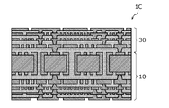
- FIG. 1 is a plan view showing an example of a wiring pattern of one wiring layer in a wiring body 30 of a mounting substrate 1 according to Embodiment 1.
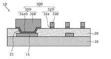
- FIG. FIG. 2 is a cross-sectional view of the inter-via wiring portion of the mounting substrate 1 along line II-II of FIG. 3 is a cross-sectional view of the interlayer connection portion of the mounting board 1 taken along line III--III in FIG.
- the mounting board 1 is, for example, a semiconductor package board, and has a plurality of wiring layers on which wiring is formed. Therefore, as shown in FIG. 1, the mounting substrate 1 includes, as the wiring bodies 30, via electrodes 31 for electrically connecting wiring between wiring layers, and wiring 32 which is wiring in one of the wiring layers. .
- the wiring 32 is connected to the via electrode 31 .
- the via electrode 31 is formed, for example, at the end of the portion where the wiring 32 extends, but it is not limited to this.
- the via electrode 31 may be formed in the middle of the wiring 32 .
- each wiring layer a plurality of via electrodes 31 and wirings 32 are formed.
- the mounting board 1 is a small ultra-high-density mounting board on which wirings 32 are mounted at high density.
- the mounting substrate 1 includes a substrate 10 and an insulating layer 20 and a wiring body 30 located on the substrate 10 .
- the wiring body 30 includes at least via electrodes 31 and wirings 32 as conductive members.
- the insulating layer 20 may be a part of the wiring body 30 .
- the substrate 10 has conductors 11 .
- the conductor 11 is, for example, a wiring or an electrode formed in a wiring layer different from the wiring 32 .
- the substrate 10 is a wiring board that is a board with wiring having wiring formed of copper foil or the like, and is, for example, a buildup board, a multilayer wiring board, a double-sided wiring board, or a single-sided wiring board. . Therefore, the substrate 10 is provided with a plurality of wirings or the like as the conductors 11 over a single layer or a plurality of layers. 2 and 3 schematically show only the conductors 11 formed on the outermost surface layer of the conductors 11 of the substrate 10. As shown in FIG.
- the mounting board 1 is an ultra-high-density mounting board
- the board 10 is a build-up board.
- the substrate 10 is not limited to a wiring substrate such as a build-up substrate, and may be an IC package substrate or an IC chip itself as long as it has wiring or electrodes as the conductor 11. good too.
- the insulating layer 20 is formed on the substrate 10 . Specifically, the insulating layer 20 covers the entire substrate 10 so as to cover the conductors 11 in the surface layer of the substrate 10 .
- the insulating layer 20 is arranged between the conductor 11 of the substrate 10 and the wiring 32 . Therefore, the insulating layer 20 is an interlayer insulating layer.
- the wiring layer in which the wiring that is the conductor 11 on the surface layer of the substrate 10 is formed is defined as the first wiring layer WL1, and the wiring 32 of the wiring body 30 is formed.
- the insulating layer 20 is an interlayer insulating layer between the first wiring layer WL1 and the second wiring layer WL2.
- a via hole 21 is formed in the insulating layer 20 .
- the via hole 21 is a through hole formed on the conductor 11 of the substrate 10 .
- a via electrode 31 is formed in the via hole 21 .
- the via hole 21 has a truncated cone shape with an inclined inner surface (tapered surface). Therefore, the opening shape (top view shape) of via hole 21 is circular, and the cross-sectional shape of via hole 21 is trapezoidal.
- the shape of the via hole 21 may be a truncated pyramid shape such as a quadrangular truncated pyramid shape, or may be a columnar shape or a prismatic shape.
- the insulating layer 20 is made of an insulating material.
- the insulating material forming the insulating layer 20 is, for example, an insulating resin.
- the insulating resin material for forming the insulating layer 20 may be a liquid insulating resin material having fluidity, which is composed of a photocurable resin such as an ultraviolet curable resin or a thermosetting resin.
- a prepreg made of a film-like insulating resin made of a thermosetting resin or a thermoplastic resin may also be used.
- An insulating resin sheet can be used as the film-like insulating resin. In this case, the insulating resin sheet preferably has adhesiveness.
- the insulating material forming the insulating layer 20 is not limited to an organic insulating material such as an insulating resin, and may be an inorganic insulating material such as a silicon oxide film or a silicon nitride film.
- the wiring body 30 is arranged on the substrate 10 having the conductor 11 .
- the via electrode 31 of the wiring body 30 is arranged on the conductor 11 of the substrate 10
- the wiring 32 of the wiring body 30 is arranged above the substrate 10 with the insulating layer 20 interposed therebetween.
- the wiring 32 is arranged on the insulating layer 20 . As shown in FIG. 2, the wiring 32 is arranged above the conductor 11 as the wiring of the substrate 10 with the insulating layer 20 interposed therebetween, but it is not limited to this.
- the wiring 32 is formed on the insulating layer 20 by a transfer method using a wiring transfer plate. It should be noted that the wiring 32 may not be entirely located on the main surface of the insulating layer 20 , and the lower portion of the wiring 32 may be located within the insulating layer 20 .
- the via electrode 31 is connected to the conductor 11 of the substrate 10 through the via hole 21 of the insulating layer 20 .
- the via electrode 31 is a plug that connects upper and lower wirings sandwiching the insulating layer 20 .
- the via electrodes 31 are composed of wirings (conductors 11) of the first wiring layer WL1 located directly below the insulating layer 20 and wirings (wirings 32) of the second wiring layer WL2 located directly above the insulating layer 20. connected to.
- At least a part of the via electrode 31 is provided inside the via hole 21 .
- the via electrode 31 is embedded in the via hole 21 without gaps.
- the via electrode 31 is formed not only inside the via hole 21 but also protruding from the main surface of the insulating layer 20 .
- the height of the via electrode 31 from the main surface of the insulating layer 20 is higher than the height of the wiring 32 from the main surface of the insulating layer 20 .
- the via electrode 31 is formed over the conductor 11 of the substrate 10 and over the insulating layer 20 .
- the via electrode 31 is formed so as to run over the main surface of the insulating layer 20 from inside the via hole 21 of the insulating layer 20 . Therefore, the planar view area of the portion of the via electrode 31 protruding from the insulating layer 20 is larger than the maximum diameter area of the portion of the via electrode 31 embedded in the via hole 21 .
- the shape of the portion of the via electrode 31 embedded in the via hole 21 is the same as the shape of the via hole 21 . Therefore, in the present embodiment, the portion of the via electrode 31 embedded in the via hole 21 has a truncated cone shape with an inclined side surface (tapered surface). The minimum diameter of the portion of the via electrode 31 embedded in the via hole 21 is larger than the width of the wiring 32 .
- the via electrode 31 has a seed layer 31a provided as a lower layer of the via electrode 31, and a via electrode body layer 31b provided on the seed layer 31a.
- seed layer 31 a is the bottom layer of via electrode 31 .
- the seed layer 31 a is formed on the conductor 11 of the substrate 10 within the via hole 21 . Specifically, seed layer 31 a is formed on the upper surface of conductor 11 so as to be in contact with conductor 11 . The seed layer 31 a is formed along the inner surface of the insulating layer 20 from above the conductor 11 within the via hole 21 .
- the seed layer 31a is formed up to the main surface of the insulating layer 20 . That is, it is formed over the conductor 11 of the substrate 10 and over the main surface of the insulating layer 20 .
- the film thickness of the seed layer 31a is constant. Therefore, the seed layer 31 a is formed so as to extend over the main surface of the insulating layer 20 from the conductor 11 in the via hole 21 .
- the seed layer 31a is a seed electrode made of a conductive material for forming the via electrode body layer 31b by plating or sputtering. Therefore, the seed layer 31a is preferably made of a conductive material with low electrical resistance.
- the seed layer 31a is a metal film made of a metal material containing copper, which is a low-resistance material, for example. In this case, the seed layer 31a may not be made of copper only, but may contain copper and other metal such as nickel. Note that the seed layer 31a may be a single film composed of only one metal film, or may be a laminated film in which a plurality of metal films are stacked.
- the via electrode body layer 31b is a plated film laminated on the seed layer 31a.
- via electrode body layer 31b is an electrolytic plated film formed by an electrolytic plating method.
- the via electrode body layer 31b is an electrolytic Cu-plated film made of copper.
- the via electrode body layer 31b is positioned on the seed layer 31a and is formed so as to fill the inside of the via hole 21 .
- the via electrode body layer 31 b is formed up to the insulating layer 20 .
- the via electrode body layer 31b is formed over the conductor 11 and the insulating layer 20 on the seed layer 31a.
- the via electrode body layer 31b is formed so as to run over the main surface of the insulating layer 20 from inside the via hole 21 of the insulating layer 20 .
- the via electrode body layer 31b constitutes most of the via electrode 31. In the present embodiment, via electrode body layer 31b occupies 90% or more of via electrode 31 in the cross-sectional view of FIG.
- the wiring 32 has an adhesion layer 32a provided as a lower layer of the wiring 32, and a wiring body layer 32b provided on the adhesion layer 32a.
- the adhesion layer 32 a is the bottom layer of the wiring 32 . Note that the adhesion layer 32 a is located within the insulating layer 20 , but may be provided on the main surface of the insulating layer 20 .
- the wiring 32 further has a conductive layer 32c provided on the wiring body layer 32b. That is, the wiring 32 has a laminated structure in which the adhesion layer 32a, the wiring body layer 32b, and the conductive layer 32c are laminated in this order in the direction away from the insulating layer 20. FIG. That is, the wiring body layer 32b is sandwiched between the adhesion layer 32a and the conductive layer 32c. The lower portion of the wiring body layer 32b and the adhesion layer 32a have the same line width.
- the adhesion layer 32a is provided to facilitate adhesion between the wiring 32 and the insulating layer 20.
- the adhesion layer 32 a has a function or structure for enhancing adhesion between the wiring 32 and the insulating layer 20 .
- the adhesion layer 32 a has a fine uneven structure as a structure for enhancing the adhesion between the wiring 32 and the insulating layer 20 .
- the adhesion layer 32a has a fine uneven structure as a whole layer, but it is not limited to this. 20 side. By providing the adhesion layer 32a having the fine uneven structure in this way, the adhesion layer 32a can be easily adhered to the insulating layer 20 by the anchor effect.
- Such a fine concavo-convex structure of the adhesion layer 32a is, for example, a needle-like concavo-convex shape with a height of 500 nm or less.
- the adhesion layer 32a is made of a metal film containing copper.
- the fine concavo-convex structure of the adhesion layer 32a is made of copper and/or copper oxide.
- a fine concave-convex structure can be formed by forming copper oxide having needle-like crystals on the copper surface and roughening the copper surface.
- the micro unevenness structure may be formed by slightly etching the copper surface by micro-roughening etching to roughen the surface.
- the adhesion layer 32a may be composed of a metal element other than copper.
- the wiring body layer 32b is a plated film laminated under the conductive layer 32c.
- the wiring body layer 32b is an electroless plated film formed by an electroless plating method.
- the wiring body layer 32b is an electroless Cu plating film made of copper.
- the wiring body layer 32b of the wiring 32 and the via electrode body layer 31b of the via electrode 31 are both Cu-plated films, but the wiring body layer 32b is an electroless Cu-plated film, and the via electrode body layer 31b is an electroless Cu-plated film.
- 31b is an electrolytic Cu plating film. Therefore, the via electrode main layer 31b and the wiring main layer 32b contain copper with different crystal grain sizes. Specifically, the average crystal grain size of copper forming the via electrode main layer 31b, which is an electrolytic Cu-plated film, is larger than the average crystal grain size of copper forming the wiring main body layer 32b, which is an electroless plated film. In other words, the average crystal grain size of copper forming the wiring body layer 32b, which is an electroless plated film, is smaller than the average crystal grain size of copper forming the via electrode body layer 31b, which is an electrolytic Cu plated film.
- Both the wiring body layer 32b of the wiring 32 and the via electrode body layer 31b of the via electrode 31 are plated films, but the wiring 32 does not have a seed layer as a lower layer. That is, the via electrode 31 has the seed layer 31a as its lower layer, but the wiring 32 does not have the seed layer as its lower layer.
- the wiring body layer 32b of the wiring 32 constitutes most of the wiring 32. In this embodiment, the wiring body layer 32b occupies 90% or more of the wiring 32 in the cross-sectional view of FIG.
- the conductive layer 32c formed on the wiring body layer 32b functions as a part of the conductor of the wiring 32 and also functions as a protective layer that protects the wiring body layer 32b. That is, when the seed layer 31a of the via electrode 31 is formed by etching and patterning the seed film, the conductive layer 32c can prevent the wiring body layer 32b from being etched and reduced. That is, when etching the seed film, the wiring body layer 32b can be protected by the conductive layer 32c. Thus, the conductive layer 32c functions as a protective layer that protects the wiring body layer 32b during etching.
- the conductive layer 32c is an electroless plated film like the wiring body layer 32b.
- the conductive layer 32c is made of a conductive material different from that of the wiring body layer 32b.
- the conductive layer 32c is made of a conductive material other than copper.
- the conductive layer 32c is made of a material containing any one of nickel (Ni), palladium (Pd), platinum (Pt), and silver (Ag). That is, the conductive layer 32c is an electroless plated film containing any of these materials.
- FIG. 4A and 4B are diagrams for explaining a method of manufacturing the wiring transfer plate 200 with wiring used when manufacturing the wiring body 30 and the mounting substrate 1 according to the first embodiment.
- 5A and 5B are diagrams for explaining a method of manufacturing the wiring transfer plate 100.
- FIG. FIG. 6A is a cross-sectional view showing a modification of the wiring transfer plate.
- FIG. 6B is a cross-sectional view of an inter-via wiring portion of the mounting board according to the modification.
- FIG. 6C is a cross-sectional view of an interlayer connection portion of a mounting substrate according to a modification.
- FIG. 7 is a diagram showing a configuration when the wiring transfer plate 200 with wiring produced in FIG. 4 is cut along another cross section.
- 8 and 9 are diagrams for explaining the method for manufacturing the wiring body 30 and the method for manufacturing the mounting board 1 according to the first embodiment.
- 8 shows a method of manufacturing a portion corresponding to the inter-via wiring portion of FIG. 2
- FIG. 9 shows a method of manufacturing a portion corresponding to the interlayer connection portion of FIG.
- the wiring body 30 and the mounting substrate 1 are produced using the wiring transfer plate 100.
- the wiring transfer plate 100 is a wiring pattern plate for forming wiring (transfer wiring) to be transferred to another member (transfer target member) in a predetermined pattern.
- the wiring transfer plate 100 in the present embodiment is a plating pattern plate for forming an electroless plating film as transfer wiring.
- the electroless plated film formed by the wiring transfer plate 100 becomes at least part of the wiring to be transferred to another member.
- a method of manufacturing the wiring body 30 and the mounting board 1 using the wiring transfer plate 100 will be described below.
- a wiring transfer plate 200 with wiring is prepared in advance.
- the wiring transfer plate 200 with wiring is obtained by forming transfer wiring on the wiring transfer plate 100 .
- the wiring transfer plate 200 with wiring is the wiring transfer plate 100 on which the transfer wiring is formed.
- wirings 32 for transferring to members constituting the mounting board 1 are formed as wirings for transfer.
- a wiring transfer plate 100 is prepared.
- the wiring transfer plate 100 is prepared in advance as shown in FIG.
- a substrate with a plating base material is received, in which a plating base material layer 130 is formed on a base material 110 serving as a support substrate.
- a highly rigid substrate such as a glass substrate or a metal substrate is preferably used.
- a metal substrate made of SUS is used as base material 110 .
- the plating base material layer 130 is a catalyst base material layer for forming an electroless plating film.
- the plating base material constituting the plating base material layer 130 one or a plurality of materials selected from nickel (Ni), palladium (Pd), platinum (Pt), chromium (Cr), iron (Fe), etc. can be used.
- the plating base material layer 130 is a nickel film.
- an insulating layer 120 that will become a transfer plate insulating layer is formed on the plating base material layer 130 .
- the insulating layer 120 for example, a photoresist can be used.
- the insulating layer 120 which is a photoresist, is exposed and developed to form a plurality of openings 121 in the insulating layer 120, and the plating base material layer 130 is formed. expose the That is, the insulating layer 120 covers the base material 110 so as to have the opening 121 on the plating base material layer 130 .
- the plating base material layer 130 functions as a release layer. good too. Giving releasability to the plating base material layer 130 means weakening the catalytic reaction effect of the plating base material layer 130 .
- the plating base material layer 130 can be provided with releasability.
- the release treatment for the plating base material layer 130 is not limited to the oxidation treatment.
- the plating base material layer 130 is a continuous film in FIG. 5, it is not limited to this.
- the plating base material layer 130 may be patterned and separated to form the plating base material layer 130A for each opening 121.
- FIG. 5 is a continuous film in FIG. 5, it is not limited to this.
- the plating base material layer 130 may be patterned and separated to form the plating base material layer 130A for each opening 121.
- the wiring 32 that will be the wiring for transfer is formed on the wiring transfer plate 100 .
- an electroless plating film (electroless plating layer) is formed on the plating base material layer 130 by an electroless plating method.
- a metal is deposited and grown by a catalytic reaction caused by the catalyst of the plating base material layer 130 , thereby forming an electroless plating film on the plating base material layer 130 .
- a conductive layer 32c and a wiring body layer 32b made of different materials are laminated as electroless plating films.
- the plating base material layer 130 is a nickel film
- a conductive layer 32c made of an electrolytic Pd-plated film is formed, and a wiring body layer 32b made of an electroless Cu-plated film is laminated on the conductive layer 32c.
- the conductive layer 32c is preferably an electroless plated film.
- the conductive layer 32c can be formed thin and with a uniform film thickness.
- the conductive layer 32c may be an electroplated film instead of an electroless plated film.
- the electroless Ni film or the electroless silver-plated film is removed without corroding Cu when forming a wiring body in a later step. Therefore, the wiring body can be easily made of only Cu. If the electroless Ni film remains, there is a concern that the wiring resistance of the wiring body will increase because the electroless Ni film generally contains substances such as boron and phosphorus and thus has high resistance. In addition, the electroless Ni film has magnetism, and there is a concern that the high-frequency characteristics and the like may be degraded. In addition, since silver is a metal that easily causes ion migration, there is a concern that reliability characteristics may deteriorate.
- FIG. 6B shows a cross-sectional view of the inter-via wiring portion of the mounting board corresponding to line II-II in FIG.
- FIG. 6C shows a cross-sectional view of the interlayer connection portion of the mounting board corresponding to line III-III in FIG.
- the conductive layer 32c remains at the connecting portion between the via electrode 31A and the wiring 32A. Good connection characteristics can be obtained as the seed layer 31a that forms the electrolytic Ni film or the electroless silver plating film and the electroless Cu film.
- the conductive layer 32c is an electroless Pd film or an electroless Pt film
- the electroless Pd film or the electroless Pt film generally contains almost no impurities, the surface resistance of the wiring can be kept low.
- it does not have magnetism, it is also advantageous in terms of high-frequency characteristics.
- Pd or Pt forming the electroless Pd film or the electroless Pt film is a metal that is more stable than Cu, it can function as a barrier layer that suppresses ion migration.
- the conductive layer 32c is preferably an electroless plated film.
- the film thickness of the conductive layer 32c can be formed to be uniform.
- the conductive layer 32c may be an electroplated film instead of an electroless plated film.
- an adhesion process is performed to impart adhesion to the surface layer of the wiring body layer 32b exposed from the insulating layer 120. Then, as shown in FIG.
- the surface layer of the wiring body layer 32b becomes the adhesion layer 32a.
- the surface layer of the wiring body layer 32b can be made into the adhesion layer 32a having a fine uneven structure.
- a wiring transfer plate 200 having wirings 32 formed on the wiring transfer plate 100 is completed. In the interlayer connection portion, the wiring transfer plate 200 with wiring has a structure as shown in FIG.
- the wiring transfer plate 200 with wiring thus manufactured can transfer the wiring 32 to another member. That is, the conductive layer 32c and the wiring body layer 32b, which are electroless plated films, and the adhesion layer 32a constitute the wiring 32, which is a transfer wiring to be transferred to another member.
- the wiring transfer plate 100 after transferring the wiring 32 of the wiring transfer plate 200 with wiring to another member returns to the state of (a) in FIG. 4 and can be used repeatedly. That is, the wiring transfer plate 100 can be reused. Specifically, as shown in (b) to (d) of FIG. 4, an electroless plating film is formed on the wiring transfer plate 100 to form the wiring 32 again, and the wiring 32 is transferred to another member. can do.
- the wiring body 30 and the mounting board 1 are manufactured by using the wiring transfer plate 200 with wiring. 8 showing the cross section of the inter-via wiring portion of the mounting board 1 and FIG. 9 showing the cross section of the interlayer connecting portion of the mounting board 1.
- FIG. 8 showing the cross section of the inter-via wiring portion of the mounting board 1
- FIG. 9 showing the cross section of the interlayer connecting portion of the mounting board 1.
- the wiring 32 is arranged on the substrate 10 with the insulating layer 20 interposed therebetween.
- the wiring 32 is formed by a transfer method using a wiring transfer plate 200 with wiring prepared in advance.
- a substrate 10 having conductors 11 is prepared.
- a build-up substrate is prepared in which wirings, electrodes, etc. are formed as conductors 11 on the uppermost layer.
- an insulating material is placed between the substrate 10 having the conductor 11 and the wiring transfer plate 200 with wiring, thereby separating the substrate 10 and the wiring.
- An insulating layer 20 is formed between the attached wiring transfer plate 200 and the wiring transfer plate 200 .
- an insulating material to be the insulating layer 20 is placed on the substrate 10 having the conductors 11, and the wiring transfer plate 200 with wires is placed on the insulating material. That is, the insulating material of the insulating layer 20 is inserted between the substrate 10 and the wiring transfer plate 200 with wiring. At this time, the wiring transfer plate 200 with wiring is arranged so that the exposed wiring 32 faces the insulating layer 20 side.
- the liquid insulating resin material is used as the insulating material for the insulating layer 20
- the liquid insulating resin material is applied onto the substrate 10 having the conductors 11, and the wiring transfer plate 200 with wiring is applied thereon. to cure the liquid insulating resin material.
- the liquid insulating resin material is a thermosetting resin
- it is cured by heating or drying
- the liquid insulating resin material is a photocurable resin
- it is cured by light irradiation.
- the insulating layer 20 can be formed between the substrate 10 and the wiring transfer plate 200 with wiring.
- the film-like insulating resin sheet is placed on the substrate 10 having the conductors 11, and the wiring transfer plate 200 with wires is placed thereon. and heat-compress. At this time, the wiring transfer plate 200 with wiring is pressed toward the substrate 10 . Thereby, the insulating layer 20 can be formed between the substrate 10 and the wiring transfer plate 200 with wiring.
- the wiring transfer plate 100 included in the wiring transfer plate 200 with wiring is separated from the insulating layer 20 . That is, the wiring transfer plate 100 and the insulating layer 20 are separated. As a result, the wiring 32 of the wiring transfer plate 200 with wiring is separated from the plating base material layer 130 (release layer) and transferred to the substrate 10 side. Specifically, the wiring 32 of the wiring transfer plate 200 with wiring is transferred to the insulating layer 20 and the wiring 32 is formed on the insulating layer 20 . In this embodiment, the conductive layer 32c, the wiring body layer 32b, and the adhesion layer 32a are transferred to the insulating layer 20. As shown in FIG.
- the wiring 32 can be easily separated from the plating base material layer 130, and the wiring 32 can be easily separated from the plating base material layer 130 by adhesion processing. Since the adhesion layer 32a is formed on the insulating layer 20, the adhesion layer 32a easily adheres to the insulating layer 20. As shown in FIG. Thereby, the wiring 32 can be easily transferred to the insulating layer 20 .
- the insulating resin sheet when a film-shaped insulating resin sheet is used as the insulating material for the insulating layer 20, the insulating resin sheet preferably has adhesiveness. This makes it easier for the adhesion layer 32a of the wiring 32 to adhere to the insulating layer 20, so that the wiring 32 can be transferred to the insulating layer 20 more easily.
- a via hole 21 is formed in the insulating layer 20 so that the conductor 11 is exposed by partially removing the insulating layer 20 .
- a via hole 21 can be formed by partially removing the insulating layer 20 by irradiating a laser from above the conductor 11 .
- the conductor 11 of the substrate 10 is exposed.
- a seed film 35 is formed to cover the exposed conductors 11 and wirings 32 .
- the seed film 35 is also laminated on the exposed insulating layer 20 .
- the seed film 35 covering the conductor 11 is a seed electrode for forming the via electrode body layer 31b of the via electrode 31 by electroplating.
- the wiring 32 can be protected by the seed film 35 until the seed film 35 is removed in subsequent steps.
- the seed film 35 covers not only the upper portion of the wiring 32 but also the side portion of the wiring 32 . Therefore, a small amount of the seed film 35 component (Pd, etc.) is present on the upper and side portions of the wiring 32 .
- the seed film 35 is formed over the entire upper surface of the substrate 10 by electroless plating or sputtering. Therefore, the seed film 35 is formed not only on the exposed surfaces of the conductors 11 and the wirings 32 but also on the exposed surfaces of the insulating layer 20 .
- the seed film 35 is a metal film made of a metal material containing copper.
- the seed film 35 may consist of only copper, or may contain copper and other metals such as nickel.
- a portion of the seed film 35 covering the wiring 32 is selected so that the portion of the seed film 35 covering the conductor 11 is exposed.
- a resist 40 is subsequently formed. Specifically, an opening 41 is formed in the resist 40 above the conductor 11 .
- a dry film resist (DFR), for example, can be used as the resist 40 .
- the via electrode body layer 31b is formed on the exposed seed film 35. Then, as shown in FIG. Specifically, the via electrode body layer 31b is formed so as to fill the inside of the opening 41 of the resist 40 .
- an electrolytic plated film is formed on the seed film 35 in the opening 41 by an electrolytic plating method as the via electrode main body layer 31b.
- the via electrode body layer 31b is an electrolytic Cu plating film.
- part of the via electrode body layer 31b is formed to run over the end of the wiring 32 in the interlayer connection. Specifically, part of the via electrode body layer 31 b is formed on the seed film 35 laminated on the wiring 32 .
- the resist 40 is removed. Specifically, the resist 40, which is a dry film resist, is removed. As a result, the portion of the seed film 35 covered with the resist 40 is exposed.
- the portion of the seed film 35 covering the wiring 32 is removed. Specifically, the exposed seed film 35 is removed by etching using an etchant. At this time, since the seed film 35 and the conductive layer 32c of the wiring 32 are made of different conductive materials, the seed film 35 can be selectively etched without etching the conductive layer 32c. By etching the seed film 35 in this way, only the seed film 35 under the via electrode body layer 31b remains, and this seed film 35 becomes the seed layer 31a, and the seed layer 31a and the via electrode body layer 31b are laminated.
- the via electrode 31 can be formed with a layered structure.
- the wiring bodies 30 having the via electrodes 31 and the wirings 32 are formed, and the mounting substrate 1 having the wiring bodies 30 can be manufactured. That is, the wiring body 30 can be manufactured on the substrate 10 having the conductor 11 , and the mounting substrate 1 with the wiring body 30 arranged on the substrate 10 can be manufactured.
- FIG. 10 is a diagram for explaining a conventional method for manufacturing a mounting substrate 1X having via electrodes 31X and wirings 32X, and shows a general semi-additive method (SAP method).
- a via hole 21 is formed above the conductor 11 by removing a portion of the insulating layer 20 with a laser, exposing the conductor 11 .
- a seed film 35X made of an electroless plated film is formed over the entire upper surface of the substrate 10 by electroless plating, as shown in FIG. 10(c). Thereby, a seed film 35X is formed on the exposed conductor 11. Next, as shown in FIG. 10(c).
- a resist 40X having openings 41X and 42X is formed.
- the opening 41X is formed in a portion corresponding to the via electrode 31X, and the opening 42X is formed in a portion corresponding to the wiring 32X.
- a dry film resist can be used as the resist 40X.
- an electrolytic plated film is formed on the seed film 35X in the openings 41X and 42X by an electrolytic plating method.
- an electroplated film to be the via electrode body layer 31b is formed on the seed film 35X covering the conductor 11 in the opening 41X, and a wiring body layer 32b is formed on the seed film 35X in the opening 42X.
- An electrolytic plated film is formed. That is, the via electrode body layer 31b and the wiring body layer 32b are formed at the same time.
- the via electrode body layer 31b and the wiring body layer 32b are electrolytic Cu plating films made of copper, for example.
- the resist 40X is removed to expose the seed film 35X.
- the exposed seed film 35X is removed by etching.
- the seed film 35X under the via electrode body layer 31b remains and becomes the seed layer 31a, forming the via electrode 31X.
- the seed film 35X under the wiring body layer 32b remains and becomes the seed layer 35a, thereby forming the wiring 32X.
- the lower layer of the wiring 32X is undercut due to overetching. That is, when the seed film 35X is etched, the line width of the lower layer of the wiring 32X is reduced. Specifically, the seed layer 35a of the wiring 32X is undercut to reduce the wiring width. As a result, a wiring defect may occur in the wiring 32X. For this reason, it is difficult to miniaturize the wiring 32X with the conventional manufacturing method of the mounting substrate 1 . In this case, the film thickness of the seed film 35X may be reduced so that the lower portion of the wiring 32X is not undercut. It is not possible.
- the lower layer of the via electrode 31 and the lower layer of the wiring 32 are made of different materials or structures.
- the lower layer of the via electrode 31 is the seed layer 31a
- the lower layer of the wiring 32 is the adhesion layer 32a
- the seed layer 31a and the adhesion layer 32a are made of different materials or structures.
- the seed layer 31a and the adhesion layer 32a both contain copper, but are made of different materials or structures.
- the seed layer 31a and the adhesion layer 32a are metal films containing copper as the same metal element, but at least one of the seed layer 31a and the adhesion layer 32a includes a metal film containing a metal element other than copper.
- the copper surface is formed to have a fine uneven structure, and the seed layer 31a and the adhesion layer 32a are made of different materials or structures.
- the lower layer of the wiring 32 is the adhesion layer 32a, and unlike the via electrode 31, the wiring 32 does not have a seed layer as a lower layer.
- the adhesion layer does not exist in the lower layer of the via electrode 31 .
- the wiring body 30 and the mounting board 1 according to the present embodiment even if the via electrodes 31 are provided, the wirings 32 can be miniaturized and narrowed in pitch.
- the method of manufacturing the wiring body 30 and the method of manufacturing the mounting board 1 include the steps of disposing the wiring 32 on the substrate 10 with the insulating layer 20 interposed therebetween, and then removing a part of the insulating layer 20. a step of forming a via hole 21 in the insulating layer 20 so that the conductor 11 of the substrate 10 is exposed by removal, and then a step of forming a seed film 35 so as to cover the exposed conductor 11 and the wiring 32.
- the wiring 32 can be protected by the seed film 35 to form the via electrode body layer 31b.
- the fine and narrow-pitch wiring 32 and the via electrodes 31 can be formed in the same wiring layer.
- the wiring 32 has an adhesion layer 32a provided as a lower layer of the wiring 32 and having a fine uneven structure, and a wiring body layer 32b provided on the adhesion layer 32a.
- the adhesion layer 32a on the wiring 32, the adhesion between the wiring 32 and the insulating layer 20 can be sufficiently ensured.
- the wiring 32 further has a conductive layer 32c provided on the wiring body layer 32b, and the conductive layer 32c is made of a conductive material different from that of the wiring body layer 32b. ing.
- the wiring body layer 32b can be protected by the conductive layer 32c. That is, selective etching using the difference in etching rate between the seed film 35 and the wiring body layer 32b becomes possible. As a result, it is possible to suppress a change in the line width of the wiring 32 due to film reduction when the seed film 35 is etched.
- the wiring 32 is formed by a transfer method. Specifically, the wiring 32 is formed using the wiring transfer plate 100 .
- the fine wiring 32 can be formed with high accuracy.
- the wiring is formed by the photolithography method, if the surface of the portion where the wiring is formed has unevenness, the focus is shifted and the fine wiring cannot be formed with high precision.
- the unevenness can be absorbed. 32 can be formed with high accuracy.
- the wiring 32 can be formed with high positioning accuracy.
- the via electrode body layer 31b and the wiring body layer 32b contain copper with different crystal grain sizes.
- the via electrode body layer 31b and the wiring body layer 32b can be formed by different manufacturing methods depending on the properties required other than low resistance.
- the via electrode body layer 31b and the wiring body layer 32b can be formed by different plating methods.
- the via electrode body layer 31b of the via electrode 31 is an electrolytic plated film formed by an electrolytic plating method, and occupies 90% or more of the via electrode 31 in a cross-sectional view.
- the via electrode body layer 31b as a relatively low-stress electrolytic plated film, it is possible to suppress the occurrence of plating peeling and cracks in the via electrode 31 due to internal stress.
- the wiring body layer 32b of the wiring 32 is an electroless plated film formed by an electroless plating method, and occupies 90% or more of the wiring 32 in a cross-sectional view.
- the line width of the wiring 32 in the present embodiment is preferably 5 ⁇ m or less, more preferably 2 ⁇ m or less.
- the wiring 32 is preferably 5 ⁇ m or less, more preferably 2 ⁇ m or less.
- the wiring body 30 manufactured in this manner can be used as a wiring layer or a redistribution layer (RDL) in a semiconductor package substrate.
- RDL redistribution layer
- the wiring body 30 can be used as a rewiring layer in the mounting board 1A, which is a 2.1D semiconductor package substrate (organic interposer).
- the mounting substrate 1B which is a 2.3D semiconductor package substrate (organic interposer).
- the substrate 10 is a buildup substrate.
- the wiring body 30 can be used as a rewiring layer in the mounting substrate 1C, which is a 2.5D semiconductor package substrate (Si or Glass interposer).
- the wiring body 30 can also be used as a rewiring layer in a mounting board that is an FO-WLP (Fan Out-Wafer Level Package).
- FO-WLP Full Out-Wafer Level Package
- mounting substrates 1A, 1B, and 1C shown in FIGS. 11 to 13 can also be applied to the following second and third embodiments.
- the wiring body 30 can also be applied to the buildup layer (wiring layer) itself of a general buildup board instead of the rewiring layer.
- the wiring body 30 can be applied to the wiring layer of the board 10, which is a buildup board shown in FIGS. 11 to 13. FIG.
- the wiring distance from the electronic component formed in the core such as an inductor or capacitor to the semiconductor is shortened, so the electrical characteristics are improved, and an interposer or rewiring layer is not required. Therefore, an inexpensive semiconductor package can be obtained.
- FIG. 14 is a cross-sectional view of a mounting board 1D according to the second embodiment.
- the wiring 32 in the first embodiment has the conductive layer 32c formed on the wiring body layer 32b, as shown in FIG. 2, the conductive layer 32c is not formed on the wiring body layer 32b. Specifically, the wiring 32D is composed only of the adhesion layer 32a and the wiring body layer 32b.
- the seed layer 31a of the via electrode 31 and the wiring body layer 32b of the wiring 32 contain the same metal.
- seed layer 31aD of via electrode 31D and wiring body layer 32b of wiring 32D contain different kinds of metals.
- both the seed layer 31a and the wiring body layer 32b are metal films containing copper, but in the present embodiment, the wiring body layer 32b is composed only of copper.
- the seed layer 31aD is a metal film containing a metal other than copper. That is, in the present embodiment, the wiring body layer 32b of the wiring 32D is the same as that of the first embodiment, but the seed layer 31aD of the via electrode 31D is different from that of the first embodiment and is made of a metal other than copper. contains.
- the wiring body 30D and the mounting structure according to the present embodiment are the same.
- the substrate 1D is the same as the wiring body 30 and the mounting substrate 1 according to the first embodiment.
- the wiring body 30D and the mounting board 1D configured in this way are manufactured by the method shown in FIG. 15A and 15B are diagrams for explaining a method for manufacturing the wiring body 30D and a method for manufacturing the mounting board 1D according to the second embodiment.
- a wiring transfer plate 200D with wiring is used in which a wiring 32D is formed on the wiring transfer plate 100.
- the wiring 32D is formed by the transfer method using the wiring transfer plate 200D with the wiring prepared in advance.
- the wiring 32D does not have the conductive layer 32c.
- the wiring 32D is composed of a wiring body layer 32b and an adhesion layer 32a.
- the wiring 32D is arranged on the substrate 10 with the insulating layer 20 interposed therebetween. Also in this embodiment, the wiring 32D is formed by the transfer method.
- a substrate 10 having conductors 11 is prepared in the same manner as in the step of FIG. 8(a).
- an insulating material is placed between the substrate 10 having the conductors 11 and the wiring transfer plate 200D with wiring, similarly to the step of FIG. 8(b).
- the insulating layer 20 is formed between the substrate 10 and the wiring transfer plate 200D.
- the wiring transfer plate 100 included in the wiring transfer plate 200D with wiring is separated from the insulating layer 20 in the same manner as in the step of FIG. 8(c).
- the wiring 32D of the wiring transfer plate 200D with wiring is separated from the plating base material layer 130 and transferred to the substrate 10 side.
- the wiring 32 ⁇ /b>D of the wiring transfer plate 200 ⁇ /b>D with wiring is transferred to the insulating layer 20 and formed on the insulating layer 20 .
- the wiring body layer 32b and the adhesion layer 32a are transferred to the insulating layer 20. As shown in FIG.
- via holes 21 are formed in the insulating layer 20 by a laser to expose the conductors 11 of the substrate 10 in the same manner as in the step of FIG. 8(d).
- a seed film 35D is formed to cover the exposed conductors 11 and wirings 32D, similarly to the step of (e) of FIG.
- the seed film 35D contains a different kind of metal than the wiring body layer 32b.
- the wiring body layer 32b is composed only of copper, but the seed film 35D contains a metal other than copper.
- the seed film 35D covering the wiring 32D is exposed so that the portion of the seed film 35D covering the conductor 11 is exposed.
- a resist 40 is selectively formed at .
- the via electrode body layer 31b is formed on the exposed seed film 35D in the same manner as in the step of FIG. 8(g). Specifically, the via electrode body layer 31b is formed so as to fill the inside of the opening 41 of the resist 40 .
- the via electrode body layer 31b is an electroplated film laminated on the seed film 35D of the opening 41 by electroplating. Specifically, the via electrode body layer 31b is an electrolytic Cu plating film.
- the resist 40 is removed in the same manner as in the step (h) of FIG. As a result, the portion of the seed film 35D covered with the resist 40 is exposed.
- the portion of the seed film 35D covering the wiring 32D is removed in the same manner as in the step (i) of FIG. Specifically, the exposed seed film 35D is removed by etching using an etchant.
- the seed film 35D can be selectively etched without etching the wiring body layer 32b. can.
- the seed film 35D By etching the seed film 35D in this way, only the seed film 35D under the via-electrode body layer 31b remains, and this seed film 35D becomes the seed layer 31aD.
- the via electrode 31D in which the seed layer 31aD and the via electrode body layer 31b are laminated can be formed.
- the wiring body 30D having the via electrode 31D and the wiring 32D is formed, and the mounting substrate 1D having the wiring body 30D can be produced. That is, the wiring body 30D can be manufactured on the substrate 10 having the conductor 11, and the mounting board 1D having the wiring body 30D arranged on the substrate 10 can be manufactured.
- the lower layer of the via electrode 31D and the lower layer of the wiring 32D are made of different conductive materials.
- the seed layer 31aD, which is the lower layer of the via electrode 31D, and the adhesion layer 32a, which is the lower layer of the wiring 32D are made of different conductive materials.
- the lower layer of the wiring 32D is the adhesion layer 32a, and the wiring 32D does not have a seed layer as a lower layer. Further, no adhesion layer exists in the lower layer of the via electrode 31D.
- the seed layer 31aD which is the lower layer of the via electrode 31D
- the seed film 35D it is possible to suppress undercutting of the lower layer of the wiring 32D due to the etching. It is possible to suppress the reduction in the line width of the lower layer of the wiring 32D.
- the wiring 32D can be miniaturized and narrowed in pitch.
- the wiring 32D does not have the conductive layer 32c, and the wiring body layer 32b is not protected by the conductive layer 32c when the seed film 35D is etched. Since the layer 32b is made of a different kind of metal, selective etching using the difference in etching rate between the seed film 35D and the wiring body layer 32b is possible. In other words, although the conductive layer 32c is not formed on the wiring body layer 32b, it is possible to prevent the wiring body layer 32b from being removed by the etchant when the seed layer 31aD is etched with the etchant. As a result, it is possible to suppress a change in the line width of the wiring 32D due to film reduction during etching of the seed film 35D.
- the wiring 32D does not have the conductive layer 32c in the present embodiment, the wiring 32D may have the conductive layer 32c.
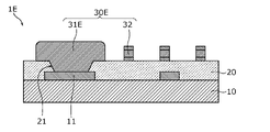
- FIG. 16 is a cross-sectional view of a mounting board 1E according to the third embodiment.
- the via electrode 31 is composed of the seed layer 31a and the via electrode body layer 31b, which is an electrolytic plated film laminated on the seed layer 31a, but is not limited to this.
- the via electrode 31E is composed of only one metal body.
- the via electrodes 31E are made of conductive paste such as silver paste.
- the wiring body 30E and the mounting board 1E according to the present embodiment are the same as the wiring body 30 and the mounting board 1 according to the first embodiment except for the configuration of the via electrodes 31E.
- the wiring body 30E and mounting substrate 1E configured in this manner are manufactured by the method shown in FIG. 17A and 17B are diagrams for explaining the method for manufacturing the wiring body 30E and the method for manufacturing the mounting substrate 1E according to the third embodiment.
- the wiring transfer plate 200 with wiring, in which the wiring 32 is formed on the wiring transfer plate 100 is used. That is, also in the present embodiment, the wiring 32 is formed by the transfer method using the wiring transfer plate 200 with wiring prepared in advance.
- the wiring 32 is arranged on the substrate 10 with the insulating layer 20 interposed therebetween.
- the steps of (a) to (c) of FIG. 17 are the same as the steps of (a) to (c) of FIG.
- via holes 21 are formed in the insulating layer 20 by a laser to expose the conductors 11 of the substrate 10, as in the process of FIG. 8(d).
- a via electrode 31E is formed to cover the exposed conductor 11. Then, as shown in (e) of FIG. 17, a via electrode 31E is formed to cover the exposed conductor 11. Then, as shown in FIG. Specifically, the via electrodes 31E are formed by applying a conductive paste.
- the wiring body 30E having the via electrode 31E and the wiring 32 is formed, and the mounting substrate 1E having the wiring body 30E can be produced. That is, the wiring body 30E can be manufactured on the substrate 10 having the conductor 11, and the mounting board 1E with the wiring body 30E arranged on the substrate 10 can be manufactured.
- the lower layer of the via electrode 31E and the lower layer of the wiring 32 are made of different conductive materials, similarly to the wiring body 30 of the above-described embodiment.
- the lower layer of the via electrode 31E is a part of the via electrode 31E made of a conductive paste, and has a different conductivity from the adhesion layer 32a that is the lower layer of the wiring 32. made up of materials.
- the via electrode 31E does not have a seed layer, it is not necessary to etch the seed layer when forming the via electrode 31E. Therefore, since the layer under the wiring 32 is not undercut when the seed layer is etched, the line width of the layer under the wiring 32 is not reduced.
- the wiring 32 can be miniaturized and the pitch can be narrowed.
- FIG. 18 is a cross-sectional view of a mounting board 1F according to the fourth embodiment.
- the wiring 32 includes an adhesion layer 32a having a fine uneven structure, a wiring body layer 32b that is an electroless Cu film, and a conductive layer 32c (protective layer) that is an electroless Cu film. Although it was configured by and, it is not limited to this.
- the wiring 32F does not have the conductive layer 32c that is the protective layer, and the adhesion layer 32aF and the wiring The main body layer 32bF.
- the adhesion layer 32aF is not formed with a micro uneven structure by copper oxide treatment or the like, but is formed by forming an organic thin film by organic adhesion treatment.
- the adhesive layer 32aF is chemically bonded to the resin forming the insulating layer 20. It is possible to form an organic thin film composed of an organic component and an organic component chemically bonded to copper constituting the wiring body layer 32bF. If the adhesion layer 32a is formed by the copper oxide treatment, the wiring 32 may be peeled off during etching because the copper oxide is vulnerable to acid. By forming, it is possible to suppress the occurrence of such a problem.
- the wiring body layer 32bF is not an electroless plated film but an electroplated film. Specifically, the wiring body layer 32bF is an electroplating film made of copper.
- another layer made of an electroless plated film may be inserted between the adhesion layer 32aF and the wiring body layer 32bF.
- the electroplated film and the electroless plated film have etching selectivity, the conductive layer 32c as a protective layer becomes unnecessary.
- the wiring body 30F and the mounting board 1F according to the present embodiment are the same as the wiring body 30 and the mounting board 1 according to the first embodiment except for the configuration of the wiring 32F. Moreover, the present embodiment can be applied not only to the first embodiment, but also to the second and third embodiments.
- the seed layer 31a of the via electrode 31 when the seed layer 31a of the via electrode 31 is formed, the seed layer 31a is formed by etching the seed film 35 covering the wiring 32 with an etchant, but the method is not limited to this. Specifically, the seed layer 31a of the via electrode 31 may be formed by a lift-off method. This method will be described with reference to FIG.
- steps (a) to (c) of FIG. 19 are the same as steps (a) to (c) of FIG.
- via holes 21 are formed in the insulating layer 20 by laser to expose the conductors 11 of the substrate 10 in the same manner as in the step (d) of FIG.
- a resist 40A is formed so as to have an opening 41A above the exposed conductor 11, and the wiring 32 is covered with the resist 40A.
- a seed film 35 is formed over the entire upper surface of the substrate 10 .
- the seed film 35 is formed separately on the conductor 11 and on the resist 40A.
- the resist 40A is removed.
- the seed film 35 on the resist 40A is removed by lift-off, leaving the seed film 35 only on the conductor 11.
- the remaining seed film 35 becomes the seed layer 31 a of the via electrode 31 .
- a via electrode body layer 31b is formed on the seed layer 31a.
- the via electrode body layer 31b made of an electrolytic plated film is formed by an electrolytic plating method.
- the via electrode body layer 31b is an electrolytic Cu plating film.
- the wiring bodies 30 having the via electrodes 31 and the wirings 32 are formed, and the mounting substrate 1 having the wiring bodies 30 can be produced. That is, the wiring body 30 can be manufactured on the substrate 10 having the conductor 11 , and the mounting substrate 1 with the wiring body 30 arranged on the substrate 10 can be manufactured. This modification can also be applied to the second embodiment.
- the insulating layer 120 which is the transfer plate insulating layer in the wiring transfer plate 100, is a resist, but the present invention is not limited to this.
- the insulating layer 120 may be an insulating resin material made of an inorganic material such as SiO2 .
- the wiring transfer plate 100B having the insulating layer 120B can be produced by the method shown in FIG.
- a substrate with a plating base material is received, which is a base material 110 serving as a support substrate and a plating base material layer 130 formed thereon.
- an insulating layer 120B (transfer plate insulating layer) made of SiO 2 is formed on the plating base material layer 130 .
- a resist 140 is formed on the insulating layer 120 .
- the resist 140 is patterned by exposing and developing the resist 140 to form an opening 141 in the resist 140 and expose the insulating layer 120 .
- plasma etching is performed using the resist 140 having the opening 141 as a mask to form the opening 121 in the insulating layer 120 and expose the plating base material layer 130 . . After that, as shown in FIG. 20(f), the resist 140 is removed. Thus, the wiring transfer plate 100B is completed.
- the electroless plated film may be an electroplated film, and the electroplated film may be an electrolytic plated film.
- the electroless plated film and the electroplated film may be plated films without distinction.
- a wiring body according to the present disclosure is useful as a wiring layer or the like in a mounting substrate such as a semiconductor package substrate.
Abstract
Description
まず、実施の形態1に係る配線体30及び実装基板1の構成について、図1~図3を用いて説明する。図1は、実施の形態1に係る実装基板1の配線体30における1つの配線層の配線パターンの一例を示す平面図である。図2は、図1のII-II線における同実装基板1のビア間配線部の断面図である。また、図3は、図1のIII-III線における同実装基板1の層間接続部の断面図である。 (Embodiment 1)
First, the configuration of the
次に、実施の形態2に係る配線体30D及び実装基板1Dについて、図14を用いて説明する。図14は、実施の形態2に係る実装基板1Dの断面図である。 (Embodiment 2)
Next, a
次に、実施の形態3に係る配線体30E及び実装基板1Eについて、図16を用いて説明する。図16は、実施の形態3に係る実装基板1Eの断面図である。 (Embodiment 3)
Next, a
次に、実施の形態4に係る配線体30F及び実装基板1Fについて、図18を用いて説明する。図18は、実施の形態4に係る実装基板1Fの断面図である。 (Embodiment 4)
Next, a
以上、本開示に係る配線体及び実装基板等について、実施の形態に基づいて説明したが、本開示は、上記実施の形態1~3に限定されるものではない。 (Modification)
As described above, the wiring body, the mounting board, and the like according to the present disclosure have been described based on the embodiments, but the present disclosure is not limited to the first to third embodiments.
10 基板
11 導電体
20 絶縁層
21 ビアホール
30、30A、30D、30E、30F 配線体
31、31A、31D、31E ビア電極
31a、31aD シード層
31b ビア電極本体層
32、32A、32D、32F 配線
32a、32aF 密着層
32b、32bF 配線本体層
32c 導電層
35、35D シード膜
40、40A レジスト
41、41A 開口部
100、100A、100B 配線転写版
110 基材
120、120B 絶縁層
121 開口部
130、130A めっき母材層
140 レジスト
141 開口部
200、200D 配線付き配線転写版 1, 1A, 1B, 1C, 1D, 1E,
Claims (14)
- 導電体を有する基板の上に配置される配線体であって、
前記基板の上に位置する絶縁層に形成されたビアホール内に設けられ、前記ビアホールを介して前記導電体に接続されたビア電極と、
前記絶縁層を介して前記基板の上方に設けられた配線と、を備え、
前記ビア電極における下部層と前記配線における下部層とは、異なる材料又は構造によって構成されている、
配線体。 A wiring body arranged on a substrate having a conductor,
a via electrode provided in a via hole formed in an insulating layer located on the substrate and connected to the conductor through the via hole;
and wiring provided above the substrate via the insulating layer,
the lower layer of the via electrode and the lower layer of the wiring are made of different materials or structures,
wiring body. - 前記ビア電極は、前記ビア電極における前記下部層として設けられたシード層と、前記シード層の上に設けられたビア電極本体層とを有する、
請求項1に記載の配線体。 The via electrode has a seed layer provided as the lower layer in the via electrode, and a via electrode body layer provided on the seed layer,
The wiring body according to claim 1. - 前記配線は、前記配線における前記下部層として設けられ、微細凹凸構造を有する密着層と、前記密着層の上に設けられた配線本体層とを有する、
請求項2に記載の配線体。 The wiring is provided as the lower layer in the wiring and has an adhesion layer having a fine uneven structure and a wiring body layer provided on the adhesion layer,
The wiring body according to claim 2. - 前記配線は、さらに、前記配線本体層の上に設けられ、前記配線本体層とは異なる材料又は構造によって構成された導電層を有する、
請求項3に記載の配線体。 The wiring further has a conductive layer provided on the wiring body layer and made of a material or structure different from that of the wiring body layer.
The wiring body according to claim 3. - 前記配線本体層と前記シード層とは、異なる種類の金属を含む、
請求項3又は4に記載の配線体。 wherein the wiring body layer and the seed layer comprise different types of metals;
The wiring body according to claim 3 or 4. - 前記ビア電極本体層と前記配線本体層とは、結晶粒径が異なる銅を含む、
請求項3~5のいずれか1項に記載の配線体。 the via electrode body layer and the wiring body layer contain copper with different crystal grain sizes,
The wiring body according to any one of claims 3 to 5. - 前記配線本体層は、無電解めっき膜であり、断面視において前記配線の90%以上を占めている、
請求項3~6のいずれか1項に記載の配線体。 The wiring body layer is an electroless plated film, and occupies 90% or more of the wiring in a cross-sectional view.
The wiring body according to any one of claims 3 to 6. - 前記ビア電極本体層は、電解めっき膜であり、断面視において前記ビア電極の90%以上を占めている、
請求項2~7のいずれか1項に記載の配線体。 The via electrode body layer is an electrolytic plating film, and occupies 90% or more of the via electrode in a cross-sectional view.
The wiring body according to any one of claims 2 to 7. - 導電体を有する基板と、
前記基板の上に位置し、請求項1~8のいずれか1項に記載の配線体と、を備える、
実装基板。 a substrate having a conductor;
A wiring body according to any one of claims 1 to 8, located on the substrate,
mounting board. - 導電体を有する基板の上に配置される配線体の製造方法であって、
前記基板の上に絶縁層を介して配線を配置する工程と、
次いで、前記絶縁層の一部を除去することで前記導電体が露出するように前記絶縁層にビアホールを形成する工程と、
次いで、露出した前記導電体及び前記配線を覆うようにシード膜を形成する工程と、
次いで、前記導電体を覆う部分の前記シード膜が露出するように前記配線を覆う前記シード膜の上に選択的にレジストを形成する工程と、
次いで、露出させた前記シード膜の上にビア電極本体層を形成する工程と、
次いで、前記レジストを除去した後に、前記配線を覆う部分の前記シード膜を除去する工程と、を含む、
配線体の製造方法。 A method for manufacturing a wiring body arranged on a substrate having a conductor, comprising:
arranging wiring on the substrate via an insulating layer;
then forming a via hole in the insulating layer to expose the conductor by removing a portion of the insulating layer;
forming a seed film to cover the exposed conductor and the wiring;
Next, a step of selectively forming a resist on the seed film covering the wiring so that the portion of the seed film covering the conductor is exposed;
then forming a via electrode body layer on the exposed seed film;
Then, after removing the resist, removing the seed film from the portion covering the wiring,
A wiring body manufacturing method. - 前記配線を配置する工程において、前記配線は、転写法によって形成される、
請求項10に記載の配線体の製造方法。 In the step of arranging the wiring, the wiring is formed by a transfer method,
The method for manufacturing the wiring body according to claim 10. - 前記配線は、配線本体層と、前記配線本体層の上に設けられ、前記配線本体層とは異なる材料又は構造からなる導電層とを有する、
請求項10又は11に記載の配線体の製造方法。 The wiring has a wiring body layer and a conductive layer provided on the wiring body layer and made of a material or structure different from that of the wiring body layer,
The method for manufacturing the wiring body according to claim 10 or 11. - 前記配線本体層と前記シード膜とは、異なる種類の金属を含む、
請求項10~12のいずれか1項に記載の配線体の製造方法。 wherein the wiring body layer and the seed film contain different types of metals,
A method for manufacturing a wiring body according to any one of claims 10 to 12. - 基板の上に配線体が配置された実装基板の製造方法であって、
前記基板の上に配線体を配置する工程を含み、
前記配線体は、請求項10~13のいずれか1項に記載の配線体の製造方法により製造される、
実装基板の製造方法。 A method for manufacturing a mounting board in which a wiring body is arranged on the board, comprising:
including a step of arranging a wiring body on the substrate;
The wiring body is manufactured by the wiring body manufacturing method according to any one of claims 10 to 13,
A method for manufacturing a mounting substrate.
Priority Applications (2)
| Application Number | Priority Date | Filing Date | Title |
|---|---|---|---|
| JP2023509070A JPWO2022202547A1 (en) | 2021-03-22 | 2022-03-16 | |
| EP22775335.7A EP4318566A1 (en) | 2021-03-22 | 2022-03-16 | Wiring body, mounting substrate, method for manufacturing wiring body, and method for manufacturing mounting substrate |
Applications Claiming Priority (2)
| Application Number | Priority Date | Filing Date | Title |
|---|---|---|---|
| JP2021-047323 | 2021-03-22 | ||
| JP2021047323 | 2021-03-22 |
Publications (1)
| Publication Number | Publication Date |
|---|---|
| WO2022202547A1 true WO2022202547A1 (en) | 2022-09-29 |
Family
ID=83397219
Family Applications (1)
| Application Number | Title | Priority Date | Filing Date |
|---|---|---|---|
| PCT/JP2022/011943 WO2022202547A1 (en) | 2021-03-22 | 2022-03-16 | Wiring body, mounting substrate, method for manufacturing wiring body, and method for manufacturing mounting substrate |
Country Status (3)
| Country | Link |
|---|---|
| EP (1) | EP4318566A1 (en) |
| JP (1) | JPWO2022202547A1 (en) |
| WO (1) | WO2022202547A1 (en) |
Citations (7)
| Publication number | Priority date | Publication date | Assignee | Title |
|---|---|---|---|---|
| JPH02113591A (en) * | 1988-10-22 | 1990-04-25 | Matsushita Electric Works Ltd | Manufacture of printed-wiring board |
| JP2006245213A (en) * | 2005-03-02 | 2006-09-14 | Shinko Electric Ind Co Ltd | Manufacturing method of wiring circuit board |
| US20080052905A1 (en) * | 2006-09-06 | 2008-03-06 | Samsung Electro-Mechanics Co., Ltd. | Fabricating method for printed circuit board |
| WO2010038559A1 (en) * | 2008-09-30 | 2010-04-08 | イビデン株式会社 | Method for manufacturing printed wiring board and printed wiring board |
| JP2013062546A (en) * | 2007-04-30 | 2013-04-04 | Samsung Electro-Mechanics Co Ltd | Carrier member for transmitting circuit, coreless printed circuit board using the same, and method of manufacturing the same |
| JP2014067941A (en) * | 2012-09-27 | 2014-04-17 | Shinko Electric Ind Co Ltd | Wiring board and manufacturing method of the same |
| JP2020107681A (en) | 2018-12-26 | 2020-07-09 | 新光電気工業株式会社 | Wiring board, semiconductor device and manufacturing method for wiring board |
-
2022
- 2022-03-16 JP JP2023509070A patent/JPWO2022202547A1/ja active Pending
- 2022-03-16 EP EP22775335.7A patent/EP4318566A1/en active Pending
- 2022-03-16 WO PCT/JP2022/011943 patent/WO2022202547A1/en active Application Filing
Patent Citations (7)
| Publication number | Priority date | Publication date | Assignee | Title |
|---|---|---|---|---|
| JPH02113591A (en) * | 1988-10-22 | 1990-04-25 | Matsushita Electric Works Ltd | Manufacture of printed-wiring board |
| JP2006245213A (en) * | 2005-03-02 | 2006-09-14 | Shinko Electric Ind Co Ltd | Manufacturing method of wiring circuit board |
| US20080052905A1 (en) * | 2006-09-06 | 2008-03-06 | Samsung Electro-Mechanics Co., Ltd. | Fabricating method for printed circuit board |
| JP2013062546A (en) * | 2007-04-30 | 2013-04-04 | Samsung Electro-Mechanics Co Ltd | Carrier member for transmitting circuit, coreless printed circuit board using the same, and method of manufacturing the same |
| WO2010038559A1 (en) * | 2008-09-30 | 2010-04-08 | イビデン株式会社 | Method for manufacturing printed wiring board and printed wiring board |
| JP2014067941A (en) * | 2012-09-27 | 2014-04-17 | Shinko Electric Ind Co Ltd | Wiring board and manufacturing method of the same |
| JP2020107681A (en) | 2018-12-26 | 2020-07-09 | 新光電気工業株式会社 | Wiring board, semiconductor device and manufacturing method for wiring board |
Also Published As
| Publication number | Publication date |
|---|---|
| JPWO2022202547A1 (en) | 2022-09-29 |
| EP4318566A1 (en) | 2024-02-07 |
Similar Documents
| Publication | Publication Date | Title |
|---|---|---|
| US7937833B2 (en) | Method of manufacturing circuit board | |
| JP5300558B2 (en) | Manufacturing method of semiconductor device | |
| TW200921876A (en) | Method for making copper-core layer multi-layer encapsulation substrate | |
| WO2011089936A1 (en) | Substrate with built-in functional element, and wiring substrate | |
| US20120279630A1 (en) | Manufacturing method of circuit substrate | |
| US7839650B2 (en) | Circuit board structure having embedded capacitor and fabrication method thereof | |
| JP2007324559A (en) | Multilayer circuit board with fine pitch and fabricating method thereof | |
| JP4758869B2 (en) | Manufacturing method of semiconductor device | |
| TW202027247A (en) | Substrate structure with high-density wiring and manufacturing method thereof | |
| JPH0536756A (en) | Tape carrier for semiconductor device and its manufacture | |
| US10874018B2 (en) | Printed wiring board having embedded pads and method for manufacturing the same | |
| TW202046840A (en) | Circuit carrier board and manufacturing method thereof | |
| WO2022202547A1 (en) | Wiring body, mounting substrate, method for manufacturing wiring body, and method for manufacturing mounting substrate | |
| WO2022202548A1 (en) | Wiring body, mounting substrate, wiring transfer plate with wiring, intermediate material for wiring body, manufacturing method for wiring body, and manufacturing method for mounting substrate | |
| US10777495B2 (en) | Printed circuit board and semiconductor package including the same | |
| WO2022202552A1 (en) | Wiring transfer plate, wiring-equipped wiring transfer plate, intermediate material for wiring body, and method for manufacturing wiring body | |
| US10897823B2 (en) | Circuit board, package structure and method of manufacturing the same | |
| WO2022202553A1 (en) | Wiring body, mounting substrate, wiring transfer board with wiring, intermediate material for wiring body, and manufacturing method for wiring body | |
| KR101272664B1 (en) | Multilayer printed circuit board including metal pattern including a seed layer and a plating layer, and method for manufacturing the same | |
| KR100925669B1 (en) | Method of fabricating a solder on pad for coreless package substrate technology | |
| KR101574019B1 (en) | Method of manufacturing Printed Circuit Board | |
| JP4445778B2 (en) | Wiring board manufacturing method | |
| KR100919632B1 (en) | Package Substrate and the Manufacturing Method Thereof | |
| KR100907721B1 (en) | Circuit board and manufacturing method thereof | |
| TWI743994B (en) | Multilayer substrate and manufacturing method thereof |
Legal Events
| Date | Code | Title | Description |
|---|---|---|---|
| 121 | Ep: the epo has been informed by wipo that ep was designated in this application |
Ref document number: 22775335 Country of ref document: EP Kind code of ref document: A1 |
|
| WWE | Wipo information: entry into national phase |
Ref document number: 2023509070 Country of ref document: JP |
|
| WWE | Wipo information: entry into national phase |
Ref document number: 18549782 Country of ref document: US |
|
| WWE | Wipo information: entry into national phase |
Ref document number: 2022775335 Country of ref document: EP |
|
| NENP | Non-entry into the national phase |
Ref country code: DE |
|
| ENP | Entry into the national phase |
Ref document number: 2022775335 Country of ref document: EP Effective date: 20231023 |