WO2022196477A1 - 画像データ処理装置、画像データ処理方法、画像データ処理プログラム及び撮像システム - Google Patents
画像データ処理装置、画像データ処理方法、画像データ処理プログラム及び撮像システム Download PDFInfo
- Publication number
- WO2022196477A1 WO2022196477A1 PCT/JP2022/010196 JP2022010196W WO2022196477A1 WO 2022196477 A1 WO2022196477 A1 WO 2022196477A1 JP 2022010196 W JP2022010196 W JP 2022010196W WO 2022196477 A1 WO2022196477 A1 WO 2022196477A1
- Authority
- WO
- WIPO (PCT)
- Prior art keywords
- pixel
- pixels
- image data
- abnormal
- data processing
- Prior art date
- Legal status (The legal status is an assumption and is not a legal conclusion. Google has not performed a legal analysis and makes no representation as to the accuracy of the status listed.)
- Ceased
Links
Images


Classifications
-
- G—PHYSICS
- G06—COMPUTING OR CALCULATING; COUNTING
- G06T—IMAGE DATA PROCESSING OR GENERATION, IN GENERAL
- G06T5/00—Image enhancement or restoration
- G06T5/77—Retouching; Inpainting; Scratch removal
-
- G—PHYSICS
- G02—OPTICS
- G02B—OPTICAL ELEMENTS, SYSTEMS OR APPARATUS
- G02B5/00—Optical elements other than lenses
- G02B5/30—Polarising elements
- G02B5/3025—Polarisers, i.e. arrangements capable of producing a definite output polarisation state from an unpolarised input state
-
- G—PHYSICS
- G06—COMPUTING OR CALCULATING; COUNTING
- G06T—IMAGE DATA PROCESSING OR GENERATION, IN GENERAL
- G06T5/00—Image enhancement or restoration
- G06T5/20—Image enhancement or restoration using local operators
-
- G—PHYSICS
- G06—COMPUTING OR CALCULATING; COUNTING
- G06T—IMAGE DATA PROCESSING OR GENERATION, IN GENERAL
- G06T5/00—Image enhancement or restoration
- G06T5/70—Denoising; Smoothing
-
- G—PHYSICS
- G06—COMPUTING OR CALCULATING; COUNTING
- G06V—IMAGE OR VIDEO RECOGNITION OR UNDERSTANDING
- G06V10/00—Arrangements for image or video recognition or understanding
- G06V10/40—Extraction of image or video features
- G06V10/60—Extraction of image or video features relating to illumination properties, e.g. using a reflectance or lighting model
-
- G—PHYSICS
- G06—COMPUTING OR CALCULATING; COUNTING
- G06V—IMAGE OR VIDEO RECOGNITION OR UNDERSTANDING
- G06V10/00—Arrangements for image or video recognition or understanding
- G06V10/70—Arrangements for image or video recognition or understanding using pattern recognition or machine learning
- G06V10/74—Image or video pattern matching; Proximity measures in feature spaces
- G06V10/75—Organisation of the matching processes, e.g. simultaneous or sequential comparisons of image or video features; Coarse-fine approaches, e.g. multi-scale approaches; using context analysis; Selection of dictionaries
- G06V10/751—Comparing pixel values or logical combinations thereof, or feature values having positional relevance, e.g. template matching
-
- G—PHYSICS
- G06—COMPUTING OR CALCULATING; COUNTING
- G06V—IMAGE OR VIDEO RECOGNITION OR UNDERSTANDING
- G06V10/00—Arrangements for image or video recognition or understanding
- G06V10/98—Detection or correction of errors, e.g. by rescanning the pattern or by human intervention; Evaluation of the quality of the acquired patterns
-
- H—ELECTRICITY
- H04—ELECTRIC COMMUNICATION TECHNIQUE
- H04N—PICTORIAL COMMUNICATION, e.g. TELEVISION
- H04N23/00—Cameras or camera modules comprising electronic image sensors; Control thereof
- H04N23/60—Control of cameras or camera modules
-
- H—ELECTRICITY
- H04—ELECTRIC COMMUNICATION TECHNIQUE
- H04N—PICTORIAL COMMUNICATION, e.g. TELEVISION
- H04N23/00—Cameras or camera modules comprising electronic image sensors; Control thereof
- H04N23/95—Computational photography systems, e.g. light-field imaging systems
-
- H—ELECTRICITY
- H04—ELECTRIC COMMUNICATION TECHNIQUE
- H04N—PICTORIAL COMMUNICATION, e.g. TELEVISION
- H04N25/00—Circuitry of solid-state image sensors [SSIS]; Control thereof
- H04N25/60—Noise processing, e.g. detecting, correcting, reducing or removing noise
- H04N25/68—Noise processing, e.g. detecting, correcting, reducing or removing noise applied to defects
-
- G—PHYSICS
- G06—COMPUTING OR CALCULATING; COUNTING
- G06T—IMAGE DATA PROCESSING OR GENERATION, IN GENERAL
- G06T2207/00—Indexing scheme for image analysis or image enhancement
- G06T2207/10—Image acquisition modality
- G06T2207/10024—Color image
Definitions
- the present invention relates to an image data processing device, an image data processing method, an image data processing program, and an imaging system, and more particularly to an image data processing device, an image data processing method, an image data processing program, and an imaging system that generate a multispectral image. .
- each optical system of the imaging lens describes a technique for capturing images corresponding to .
- an image corresponding to each optical system is generated by performing predetermined interference removal processing on image data output from an imaging device.
- the content of interference removal processing is changed depending on the presence or absence of saturated pixels.
- Patent Document 2 describes a technique for processing image data captured by a so-called polarization imaging device to detect defective pixels.
- An embodiment according to the technology of the present disclosure provides an image data processing device, an image data processing method, an image data processing program, and an imaging system capable of generating a high-quality multispectral image.
- an image data processing device for processing image data captured by an imaging device comprising: a processor, the processor performing processing for acquiring image data and pixel values from the acquired image data; A process of detecting a pixel out of a predetermined range as an abnormal pixel, a process of correcting the pixel value of the abnormal pixel based on the pixel values of surrounding pixels when the abnormal pixel is detected, and a process of correcting the pixel value of the abnormal pixel based on the pixel values of the surrounding pixels when the abnormal pixel is detected. and generating an image of spectrally separated wavelengths from image data after correcting the pixel values of the abnormal pixels.
- the processor does not correct the pixel value of the abnormal pixel, and generates an image of the spectral wavelength from the image data excluding the abnormal pixel.
- the process of detecting an abnormal pixel includes a process of detecting a set of pixels including the abnormal pixel and a process of identifying the abnormal pixel from the set of detected pixels; Any one image data processing device.
- the process of detecting a set of pixels including an abnormal pixel is the sum of the pixel values of the pixels that make up the set of pixels, or the sum of the pixel values of the pixels that make up the set of pixels multiplied by a specific coefficient.
- the image data processing device wherein the sum is calculated, and a set of pixels whose calculated sum is equal to or greater than a first threshold value is detected as a set of pixels including an abnormal pixel.
- the process of identifying an abnormal pixel extracts a pixel whose pixel value is equal to or less than the second threshold and/or a pixel whose pixel value is a saturated value from a set of pixels including the abnormal pixel, and identifies the abnormal pixel.
- the image data processing device according to (5) or (6).
- the process of identifying an abnormal pixel includes a process of detecting a set of pixels containing an abnormal pixel from among sets of pixels surrounding the set of pixels containing an abnormal pixel, and a process of detecting a set of pixels containing an abnormal pixel.
- the image data processing device of (8) comprising a process of identifying an abnormal pixel from within a set of pixels containing the abnormal pixel based on the above.
- the process of identifying an abnormal pixel includes a process of estimating the pixel value of a pixel from the pixel values of surrounding pixels, and a process of identifying a pixel whose difference from the estimated pixel value is equal to or greater than a third threshold as an abnormal pixel.
- the image data processing device of (8) comprising:
- An optical system that splits incident light into a plurality of wavelengths, polarizes the split wavelengths of light in a specific direction, and multiple sets of pixels equipped with different types of polarizers.
- An image data processing method for processing image data captured by an imaging device including an imaging device comprising: a process of acquiring image data; is detected as an abnormal pixel; if an abnormal pixel is detected, the pixel value of the abnormal pixel is corrected based on the pixel values of surrounding pixels; and generating an image of spectrally divided wavelengths from the image data after correcting the pixel values.
- An optical system that splits incident light into a plurality of wavelengths, polarizes the split wavelengths of light in a specific direction, and multiple sets of pixels that are equipped with different types of polarizers.
- An image data processing program for processing image data captured by an imaging device comprising an imaging device comprising: a function of acquiring image data; A function of detecting an abnormal pixel, a function of correcting the pixel value of the abnormal pixel based on the pixel values of the surrounding pixels when the abnormal pixel is detected, and a function of correcting the pixel value of the abnormal pixel when the abnormal pixel is detected.
- An image data processing program that causes a computer to realize a function of generating an image of spectral wavelengths from image data whose values have been corrected.
- An optical system that splits incident light into a plurality of wavelengths, polarizes the split wavelengths of light in a specific direction, and multiple sets of pixels that are equipped with different types of polarizers. and an image data processing device according to any one of (1) to (12) for processing image data captured by the imaging device.
- FIG. 1 is a diagram showing a schematic configuration of a multispectral camera system to which the present invention is applied;
- FIG. Exploded view showing the schematic configuration of the filter unit
- Block diagram of the functions realized by the image data processing device Flowchart showing a processing procedure for detecting an abnormal pixel
- Flowchart showing image data processing procedure Flowchart showing procedure of processing for detecting and correcting abnormal pixels
- a diagram showing an outline of processing when performing interference removal processing using a conventional method A diagram showing an outline of processing when interference removal processing is performed by the technique of the first embodiment.
- Block diagram of the functions realized by the image data processing device A diagram showing an outline of the processing when the interference removal processing is performed by the second method.
- 4 is a flow chart showing a procedure for processing image data by an image data processing device;
- Conceptual diagram of a method for identifying abnormal pixels using a set of surrounding pixels A diagram showing a set of 8 surrounding pixels
- Conceptual diagram for identifying abnormal pixels by expanding the range of reference pixel sets A diagram showing a set of 8 surrounding pixels
- FIG. 1 is a diagram showing a schematic configuration of a multispectral camera system to which the present invention is applied.
- the multispectral camera system is a system that simultaneously captures images that are split into multiple wavelengths.
- the captured image is called a multispectral image.
- the multispectral camera system 1 shown in FIG. 1 is a so-called polarized multispectral camera system, and shows an example of capturing an image split into three wavelengths.
- a polarization method is a multispectral camera system that uses polarized light.
- the multispectral camera system 1 of the present embodiment is mainly composed of a multispectral camera 10 and an image data processing device 300.
- the multispectral camera system 1 is an example of an imaging system.
- a multispectral camera 10 according to the present embodiment is mainly composed of a lens device 100 and a camera body 200 .
- Multispectral camera 10 is an example of an imaging device.
- the lens device 100 splits incident light into a plurality of wavelengths, polarizes the split wavelengths of light in a specific direction, and emits the polarized light. In this embodiment, incident light is split into three wavelengths.
- Lens device 100 is an example of an optical system.
- the lens device 100 includes a plurality of lens groups 110A and 110B and a filter unit 120.
- the lens groups 110A and 110B are composed of at least one lens. In FIG. 1, only two lens groups 110A and 110B are shown for convenience.
- the lens group 110A arranged on the front side of the filter unit 120 is defined as the first lens group
- the lens group 110B arranged on the rear side of the filter unit 120 is defined as the second lens group. , 110B.
- the "front side” means the "object side”
- the "back side” means the "image side”.
- the filter unit 120 is arranged in the optical path. More specifically, the filter unit 120 is arranged at or near the pupil position in the lens apparatus 100 .
- the vicinity of the pupil position refers to an area that satisfies the following formula.
- FIG. 2 is an exploded view showing a schematic configuration of the filter unit.
- the filter unit 120 is composed of a filter frame 122 having a plurality of windows (openings) and a plurality of filters (optical elements) attached to each window of the filter frame 122 .
- the filter frame 122 of this embodiment has a disk-like shape and has three windows 122A, 122B, and 122C.
- the three windows 122A, 122B, 122C are circular openings arranged at equal intervals along the circumferential direction.
- the window portion indicated by reference numeral 122A is referred to as a first window portion
- the window portion indicated by reference numeral 122B is referred to as a second window portion
- the window portion indicated by reference numeral 122C is referred to as a third window portion.
- 122B, 122C is referred to as a third window portion.
- the two filters are attached to each of the three windows 122A, 122B, and 122C.
- the two filters are composed of band-pass filters (BPF) 123A, 123B and 123C and polarized light filters (PLF) 124A, 124B and 124C.
- BPF band-pass filters
- PPF polarized light filters
- Bandpass filters 123A, 123B, and 123C which transmit light in different wavelength ranges, are attached to the three windows 122A, 122B, and 122C.
- the transmission wavelength ranges of the bandpass filters 123A, 123B, and 123C attached to the three windows 122A, 122B, and 122C are the wavelength ranges of the three images to be picked up. That is, it becomes the wavelength range of the multispectral image to be captured.
- a bandpass filter 123A that transmits light in the first wavelength band ⁇ 1 is attached to the first window portion 122A.
- the bandpass filter 123A attached to the first window portion 122A will be referred to as the first bandpass filter 123A to distinguish it from other bandpass filters, as required.
- a bandpass filter 123B that transmits light in the second wavelength region ⁇ 2 is attached to the second window portion 122B.
- the bandpass filter 123B attached to the second window portion 122B will be referred to as a second bandpass filter 123B to distinguish it from other bandpass filters, as required.
- a bandpass filter 123C that transmits light in the third wavelength band ⁇ 3 is attached to the third window portion 122C.
- the bandpass filter 123C attached to the third window portion 122C will be referred to as a third bandpass filter 123C to distinguish it from other bandpass filters, as required.
- bandpass filters 123A, 123B, and 123C are preferable to use reflective filters for the bandpass filters 123A, 123B, and 123C from the viewpoint of a high degree of freedom in spectral transmission characteristics.
- Polarizing filters 124A, 124B, and 124C having different transmission axis angles (transmission axis directions) are attached to the three windows 122A, 122B, and 122C, respectively.
- a polarizing filter 124A whose transmission axis is set at a first angle ⁇ 1 (first direction) is attached to the first window portion 122A.
- a polarizing filter 124A with a transmission axis set at 0° is attached.
- the polarizing filter 124A attached to the first window portion 122A will be referred to as a first polarizing filter 124A to distinguish it from other polarizing filters, as required.
- a polarizing filter 124B whose transmission axis is set at a second angle ⁇ 2 (second direction) is attached to the second window portion 122B.
- a polarizing filter 124B with a transmission axis set at 60° is attached.
- the polarizing filter 124B attached to the second window portion 122B will be referred to as a second polarizing filter 124B as needed to distinguish it from other polarizing filters.
- a polarizing filter 124C whose transmission axis is set at a third angle ⁇ 3 (third direction) is attached to the third window portion 122C.
- a polarizing filter 124A with a transmission axis set at 120° is attached.
- the polarizing filter 124C attached to the third window portion 122C will be referred to as a third polarizing filter 124C as needed to distinguish it from other polarizing filters.
- the angle of the transmission axis is 0° when it is parallel to the X axis, and the counterclockwise direction as viewed from the object side (front side) is the plus (+) direction. Therefore, when the transmission axis is 60°, it means that the transmission axis is inclined 60° counterclockwise with respect to the X axis. Also, the transmission axis of 120° means that the transmission axis is tilted counterclockwise by 120° with respect to the X-axis.
- the X-axis is an axis set on a plane orthogonal to the optical axis Z.
- the axis perpendicular to the X axis is the Y axis.
- the imaging element provided in the camera body 200 is arranged such that the upper and lower sides of its light receiving surface are parallel to the X-axis. Also, the left and right sides are arranged parallel to the Y-axis.
- the polarizing filters 124A, 124B, and 124C are preferably of the absorption type from the viewpoint of ghost suppression.
- the light incident on the lens device 100 is split into three wavelengths in the process of passing through the filter unit 120, and the light is polarized in a specific vibration direction for each wavelength and emitted. Specifically, light in a first wavelength band ⁇ 1 polarized in a first direction, light in a second wavelength band ⁇ 2 polarized in a second direction, and a third wavelength polarized in a third direction The light in the region ⁇ 3 and the light in the region ⁇ 3 are emitted separately.
- the camera body 200 has an imaging device 210 as shown in FIG.
- the imaging device 210 is arranged on the optical axis of the lens device 100 and receives light that has passed through the lens device 100 .
- This imaging device 210 is configured by a so-called polarization imaging device.
- a polarization imaging device is an imaging device equipped with a polarizer, and a polarizer is provided for each pixel.
- a polarizer is provided, for example, between the microlens and the photodiode.
- this type of polarization imaging device is publicly known, a detailed description thereof will be omitted (see, for example, International Publication No. 2020/071253).
- the type of polarizer (angle of transmission axis) mounted on the imaging device 210 is selected according to the number of wavelengths to be imaged.
- a polarizing imaging device having polarizers in at least three directions is used.
- a polarizing imaging device having polarizers in four directions is used.
- FIG. 3 is a diagram showing an example of arrangement of pixels and polarizers in an imaging device.
- a polarizer with a transmission axis angle of ⁇ 1 is a first polarizer
- a polarizer with a transmission axis angle of ⁇ 2 is a second polarizer
- a polarizer with a transmission axis angle of ⁇ 3 is a third polarizer
- a transmission axis is A polarizer having an angle of ⁇ 4 is referred to as a fourth polarizer.
- the angle ⁇ 1 of the transmission axis of the first polarizer is 0°
- the angle ⁇ 2 of the transmission axis of the second polarizer is 45°
- the angle ⁇ 3 of the transmission axis of the third polarizer is is set to 90°
- the angle ⁇ 4 of the transmission axis of the fourth polarizer is set to 135°.
- the pixel P1 with the first polarizer is the first pixel
- the pixel P2 with the second polarizer is the second pixel
- the pixel P3 with the third polarizer is the third pixel
- the fourth polarizer. is the fourth pixel. 2 ⁇ 2 pixels consisting of the first pixel P1, the second pixel P2, the third pixel P3, and the fourth pixel P4 constitute one pixel set SP, and this pixel set SP is repeatedly arranged along the X-axis and the Y-axis. be done.
- an imaging device equipped with polarizers in four directions can capture polarized images in four directions in one shot.
- the imaging device 210 is configured, for example, as a CMOS (Complementary Metal Oxide Semiconductor) type that includes a drive section, an ADC (Analog to Digital Converter), a signal processing section, and the like.
- the imaging element 210 operates by being driven by a built-in driving unit.
- the signal of each pixel is converted into a digital signal by the built-in ADC and output.
- the signal of each pixel is output after undergoing correlated double sampling processing, gain processing, correction processing, etc. by the built-in signal processing unit.
- the signal processing may be performed after conversion into a digital signal, or may be performed before conversion into a digital signal.
- the output Vout (signal value of each pixel) of the imaging device 210 is, for example, as shown in the following formula.
- Vout (Vin - Vth) x Gain
- Vin is a voltage generated by incident light
- Vth is a threshold voltage
- Gain is a gain
- the range of Vout is 0-255. Therefore, if the incident light is too strong, saturated pixels will occur. For example, in the case of 8 bits, even if the output voltage is 255 or more, it is expressed as 255. Further, the output of the defective pixel is 0 or a value close to 0 only for that pixel.
- the camera body 200 includes an output unit (not shown) that outputs image data captured by the image sensor 210, a camera control unit (not shown) that controls the overall operation of the camera body 200, and the like.
- the camera control section is composed of, for example, a micro processing unit (MPU) having a processor and memory.
- the microprocessing unit functions as a camera control section by executing a predetermined control program.
- the image data output from the camera body 200 is so-called RAW image data. That is, unprocessed image data.
- This RAW image data is processed by the image data processing device 300 to generate an image spectrally divided into a plurality of wavelengths.
- the image data processing device 300 processes image data (RAW image data) output from the camera body 200 of the multispectral camera 10 to generate an image spectrally divided into a plurality of wavelengths. Specifically, the wavelengths corresponding to the transmission wavelength ranges ⁇ 1, ⁇ 2, and ⁇ 3 of the bandpass filters 123A, 123B, and 123C attached to the window portions 122A, 122B, and 122C of the filter unit 120 built in the lens device 100 are Generate an image.
- image data RAW image data
- FIG. 4 is a diagram showing an example of the hardware configuration of the image data processing device.
- the image data processing device 300 includes a CPU (Central Processing Unit) 311, a ROM (Read Only Memory) 312, a RAM (Random Access Memory) 313, an auxiliary storage device 314, an input device 315, and an output device 316. and an input/output interface (I/F) 317 and the like.
- a CPU Central Processing Unit
- ROM Read Only Memory
- RAM Random Access Memory
- I/F input/output interface
- Such an image data processing device 300 is configured by, for example, a general-purpose computer such as a personal computer.
- the image data processing device 300 functions as an image data processing device when the CPU 311, which is a processor, executes a predetermined program (image data processing program). Programs executed by the CPU 311 are stored in the ROM 312 or the auxiliary storage device 314 .
- the auxiliary storage device 314 constitutes a storage unit of the image data processing device 300 .
- the auxiliary storage device 314 is composed of, for example, an HDD (Hard Disk Drive), an SSD (Solid State Drive), or the like.
- the input device 315 constitutes an operation unit of the image data processing device 300 .
- the input device 315 is composed of, for example, a keyboard, mouse, touch panel, and the like.
- the output device 316 constitutes the display section of the image data processing device 300 .
- the output device 316 is configured by, for example, a display such as a liquid crystal display (Liquid Crystal Display) or an organic EL display (Organic Light Emitting Diode display).
- the input/output interface 317 constitutes a connection section of the image data processing device 300 .
- the image data processing device 300 is connected to the camera body 200 of the multispectral camera 10 via the input/output interface 317 .
- FIG. 5 is a block diagram of functions realized by the image data processing device.
- the image data processing device 300 functions as an image data acquisition unit 320, an abnormal pixel detection unit 321, a pixel value correction unit 322, an image generation unit 323, an output control unit 324, and a recording control unit 325. come true. These functions are realized by the CPU 311 executing a predetermined program (image data processing program).
- the image data acquisition unit 320 acquires image data obtained by imaging from the multispectral camera 10 .
- the image data obtained from the multispectral camera 10 is RAW image data.
- Image data is obtained through the input/output interface 317 .
- the abnormal pixel detection unit 321 analyzes the acquired image data and performs processing for detecting abnormal pixels.
- an abnormal pixel is a pixel whose pixel value is out of a predetermined range, that is, a pixel with an inappropriate luminance value.
- Abnormal pixels include defective pixels and saturated pixels.
- a defective pixel is a pixel whose pixel value is out of a predetermined range due to a failure.
- a saturated pixel is a pixel whose pixel value is out of a predetermined range due to saturation.
- a faulty pixel has a pixel value of 0 or close to 0.
- a saturated pixel has a saturated pixel value. For example, in the case of 8 bits, it is 255.
- the image data processing apparatus 300 of the present embodiment detects abnormal pixels in captured image data, corrects them, and generates an image of each wavelength.
- Abnormal pixels are detected in units of pixel sets SP.
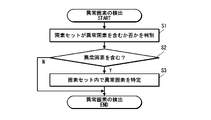
- FIG. 6 is a flow chart showing the processing procedure for detecting an abnormal pixel.
- step S1 a process of determining whether or not the target pixel set SP includes an abnormal pixel is performed (step S2).
- step S2 it is determined whether or not the target pixel set SP includes an abnormal pixel (step S2). If it is determined that the target pixel set SP does not contain an abnormal pixel, the abnormal pixel detection processing for the pixel set ends.
- step S3 a process of specifying an abnormal pixel in the target pixel set SP is performed (step S3).
- the process of determining whether or not the target pixel set SP includes an abnormal pixel is performed based on the signal values (pixel values) of the four pixels P1, P2, P3, and P4 that make up the pixel set SP.
- the imaging device 210 used in the multispectral camera 10 of this embodiment is a polarization imaging device.
- the outputs of pixels in each pixel set have a certain relationship. That is, based on the setting of the angle of the transmission axis of the polarizer mounted on each pixel, a certain relationship is established between the output signals.
- one pixel set SP is composed of four pixels P1 to P4, each having polarizers of 0°, 45°, 90°, and 135°. The relationship of formula (1) holds. However, it is assumed that the same amount of light is incident on each of the pixels P1 to P4.
- x1+x3 x2+x4 (1)
- x1 is the pixel value of the first pixel P1, that is, the pixel value of the pixel where the angle of the transmission axis of the polarizer is 0°.
- x2 is the pixel value of the second pixel P2, that is, the pixel value of the pixel in which the angle of the transmission axis of the polarizer is 45°.
- x3 is the pixel value of the third pixel P3, that is, the pixel value of the pixel in which the angle of the transmission axis of the polarizer is 90°.
- x4 is the pixel value of the fourth pixel P4, that is, the pixel value of the pixel in which the angle of the transmission axis of the polarizer is 135°.
- the image data processing apparatus 300 of the present embodiment uses the relationship represented by the above equation (1) to determine whether or not the target pixel set SP includes an abnormal pixel.
- E is calculated by the following formula (2), and when E is equal to or greater than the threshold value Th1, it is determined that the target pixel set SP includes an abnormal pixel.
- the process of identifying the abnormal pixel in the pixel set SP is performed as follows. That is, pixels whose pixel values are equal to or less than the threshold value Th2 and pixels whose pixel values are saturated are extracted from the target pixel set SP, and the extracted pixels are specified as abnormal pixels.
- the process of extracting pixels whose pixel values are equal to or less than the threshold Th2 is the process of extracting faulty pixels.
- a faulty pixel has an output of 0 or close to 0. Therefore, pixels with pixel values of 0 or close to 0 are extracted to specify faulty pixels. Therefore, the threshold Th2 is set to 0 or a value close to 0.
- the threshold Th2 is an example of a second threshold.
- the process of extracting pixels whose pixel values are saturated is the process of extracting saturated pixels.
- a saturated pixel has a saturated pixel value. Therefore, a saturated pixel is specified by extracting a pixel having a saturated pixel value.
- the saturation value is 255 when the output of the image sensor 210 is 8 bits.
- the pixel value correction unit 322 When an abnormal pixel is detected, the pixel value correction unit 322 performs processing for correcting the pixel value of the abnormal pixel.
- the pixel value correction unit 322 corrects the pixel value of the abnormal pixel based on the pixel values of the pixels surrounding the abnormal pixel.
- the pixel value of the abnormal pixel is corrected based on the pixel values of other pixels in the pixel set in which the abnormal pixel is detected. That is, since the pixel values of pixels in the same pixel set have the relationship of the above equation (1), the pixel values of the abnormal pixels are estimated and corrected using the relationship of the above equation (1).
- the pixel value x1 of the first pixel P1 is 180
- the pixel value x2 of the second pixel P2 is 158.0385
- the pixel value x3 of the third pixel P3 is 240
- the pixel value x4 of the fourth pixel P4 is 255. do.
- the fourth pixel P4 is an abnormal pixel.
- the image generation unit 323 performs processing for generating images of a plurality of wavelengths by performing predetermined signal processing on image data obtained by imaging. At this time, when processing for correcting pixel values is performed, predetermined signal processing is performed on the corrected image data to generate images of a plurality of wavelengths.
- the images of multiple wavelengths are images of wavelengths separated by the lens device 100 of the multispectral camera 10 . Specifically, it is an image of the transmission wavelength range of the band-pass filters 123A, 123B, and 123C attached to the windows 122A, 122B, and 122C of the filter unit 120.
- an image of the first wavelength range ⁇ 1 (first image), an image of the second wavelength range ⁇ 2 (second image), and an image of the third wavelength range ⁇ 3 (third image) to generate
- the image generation unit 323 performs processing (interference removal processing) to remove interference in units of pixel sets from the image data acquired by the image data acquisition unit 320, and generates images in the respective wavelength ranges ⁇ 1, ⁇ 2, and ⁇ 3. do. This process will be outlined below.
- an imaging device equipped with polarizers in four directions can capture polarized images in four directions in one shot.
- the image components of the respective wavelength regions ⁇ 1, ⁇ 2, and ⁇ 3 are included in the four-direction polarized images at a predetermined ratio (interference rate).
- the interference rate is determined by the angles ⁇ 1, ⁇ 2, and ⁇ 3 of the transmission axes of the polarizing filters 124A, 124B, and 124C attached to the windows 122A, 122B, and 122C of the filter unit 120, and the pixels P1, P2, and P3 of the image sensor 210. , and the angle of the transmission axis of the polarizer provided at P4.
- the angles ⁇ 1, ⁇ 2, and ⁇ 3 of the transmission axes of the polarizing filters 124A, 124B, and 124C attached to the windows 122A, 122B, and 122C, and the polarizers provided to the pixels P1, P2, P3, and P4 is obtained by the square of the cosine (cos) of the angular differences between the transmission axis angles ⁇ 1, ⁇ 2, ⁇ 3, and ⁇ 4 of . Therefore, for example, the ratio (interference rate) of light passing through the first window portion 122A (light passing through the first polarizing filter 124A) received by the first pixel P1 is cos 2 (
- the interference rate is known, and by using this known interference rate information, images for each wavelength can be generated. Specifically, an image of each wavelength is generated as follows.
- x1 be the pixel value of the first pixel P1
- x2 be the pixel value of the second pixel P2
- x3 be the pixel value of the third pixel P3
- x4 be the pixel value of the fourth pixel P4 in the image captured by the imaging device 210.
- X1 be the pixel value of the corresponding pixel of the generated first image
- X2 be the pixel value of the corresponding pixel of the second image
- X3 be the pixel value of the corresponding pixel of the third image.
- b11 is the rate at which light in the first wavelength range ⁇ 1 is received by the first pixel P1
- b12 is the rate at which the light in the second wavelength range ⁇ 2 is received by the first pixel P1
- light in the third wavelength range ⁇ 3. is received by the first pixel P1 is b13
- the following relationship holds between X1, X2, X3 and x1.
- b11*X1+b12*X2+b13*X3 x1 (3-1)
- b21 is the rate at which the light in the first wavelength range ⁇ 1 is received by the second pixel P2
- b22 is the rate at which the second pixel P2 receives light in the second wavelength range ⁇ 2
- b22 is the rate at which the light in the second wavelength range ⁇ 2 is received by the second pixel P2
- light received by the second pixel P2 is b23, the following relationship holds between X1, X2, X3 and x2.
- b21*X1+b22*X2+b23*X3 x2 (3-2)
- b31 is the rate at which light in the first wavelength range ⁇ 1 is received by the third pixel P3
- b32 is the rate at which the third pixel P3 receives light in the second wavelength range ⁇ 2
- b32 is the rate at which the light in the second wavelength range ⁇ 2 is received by the third pixel P3.
- light received by the third pixel P3 is b33, the following relationship holds between X1, X2, X3 and x3.
- b31*X1+b32*X2+b33*X3 x3 (3-3)
- b41 is the rate at which the light in the first wavelength range ⁇ 1 is received by the fourth pixel P
- b42 is the rate at which the fourth pixel P4 receives light in the second wavelength range ⁇ 2, and the third wavelength range ⁇ 3.
- light received by the fourth pixel P4 is b43, the following relationship holds between X1, X2, X3 and x4.
- b41*X1+b42*X2+b43*X3 x4 (3-4)
- matrix A be the inverse matrix B ⁇ 1 of matrix B.
- X1, X2, and X3 can be calculated by multiplying both sides of the above formula (4) by matrix A. That is, it can be calculated by the following formula (5).
- Matrix A is an interference cancellation matrix.
- the image data processing device 300 holds each element (a11, a12, . . . ) of the interference cancellation matrix A as a coefficient group.
- the coefficient group information is stored, for example, in the auxiliary storage device 314 .
- the image generation unit 323 acquires information on the coefficient group from the auxiliary storage device 314, performs interference elimination processing, and generates an image of each wavelength.
- the output control unit 324 controls the output of the images of each wavelength (first image, second image and third image) generated by the image generation unit 323 .
- output to the display which is the output device 316, is controlled.
- the recording control unit 325 controls recording of images of each wavelength generated by the image generation unit 323 in accordance with instructions from the user.
- the generated image of each wavelength is recorded in the auxiliary storage device 314 .
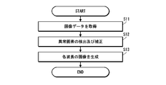
- FIG. 7 is a flow chart showing the procedure for processing image data.
- step S11 a process of acquiring image data from the multispectral camera 10 is performed.
- step S12 processing for detecting and correcting abnormal pixels from the acquired image data is performed.
- step S13 a process of generating an image of each wavelength is performed.
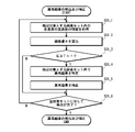
- FIG. 8 is a flowchart showing the procedure of processing for detecting and correcting abnormal pixels.
- the process of detecting abnormal pixels is performed in units of pixel sets.
- information on the pixel values x1 to x4 of the pixels P1 to P4 in the pixel set to be detected is obtained (step S21_1).
- the calculated strength value E is compared with the threshold value Th1, and it is determined whether the strength value E is equal to or greater than the threshold value Th1 (step S21_3).
- the case where the intensity value E is equal to or greater than the threshold Th1 means that the target pixel set includes an abnormal pixel.
- the intensity value E is less than the threshold Th1, the target pixel set does not include any abnormal pixels.
- processing for identifying an abnormal pixel is performed (step S21_4). This processing is performed by extracting pixels whose pixel values are equal to or less than the threshold value Th2 and pixels whose pixel values are saturation values from the target pixel set.
- the abnormal pixel processing for the target pixel set ends. After that, it is determined whether detection of abnormal pixels has been completed for all pixel sets (step S21_6). If the detection of abnormal pixels has not been completed for all pixel sets, the pixel value information of the next pixel set is obtained (step S21_1), and the detection of abnormal pixels is performed in the same manner. When the detection of abnormal pixels is completed for all pixel sets, the process of detecting and correcting abnormal pixels ends.
- an image for each wavelength is generated based on the corrected image data.
- the image data processing apparatus 300 of the present embodiment when an image data captured contains an abnormal pixel, the pixel value is corrected, so that a high-quality image can be generated. . That is, if interference removal processing is performed while including an abnormal pixel, the generated image may be corrupted. Since removal processing is performed, a high-quality image can be generated.
- Example The following shows a comparison of the effect with interference cancellation processing using a conventional method.
- FIG. 9 is a diagram showing an outline of processing when performing interference removal processing using a conventional method.
- FIG. 10 is a diagram showing an outline of processing when interference elimination processing is performed by the technique of the above embodiment.
- the conventional method is a method of performing interference removal processing as it is without performing any processing, even if an abnormal pixel is included.
- FIGS. 9 and 10 show examples when light of each wavelength is incident on a certain pixel set with the following intensity. That is, an example in which the light in the first wavelength range ⁇ 1 is 100, the light in the second wavelength range ⁇ 2 is 100, and the light in the third wavelength range ⁇ 3 is 220 is shown.
- FIGS. 9 and 10 show examples when light is incident on each pixel P1 to P4 in the pixel set with the following intensity. That is, the first pixel P1 is 180, the second pixel is 158.0385, the third pixel P3 is 240, and the fourth pixel P4 is 261.9615.
- FIGS. 9 and 10 show examples when the output of the imaging device is 8 bits.
- the signal value (pixel value) of each pixel actually output from the image sensor is as follows. That is, the first pixel P1 is 180, the second pixel is 158.0385, the third pixel P3 is 240, and the fourth pixel P4 is 255. That is, the pixel value of the fourth pixel P4 is output as the saturated value (255).
- an image of each wavelength can be generated even if abnormal pixels are removed.
- the number of pixels required to generate an image of each wavelength is three.
- one pixel set may consist of three pixels (pixels with polarizers in three directions). Therefore, if one pixel set consists of four pixels (pixels with polarizers in four directions), there is redundancy, and even if one pixel is omitted, an image of each wavelength can be generated. . That is, interference can be eliminated.
- an image for each wavelength is generated by changing the interference cancellation matrix. That is, interference cancellation processing is performed by changing the interference cancellation matrix.
- a pixel that has become an abnormal pixel due to a failure outputs an abnormal signal value each time. That is, the same pixel becomes an abnormal pixel each time. If the same pixel becomes an abnormal pixel every time, since the position of the abnormal pixel is known, a method of generating an image of each wavelength from the image data excluding the abnormal pixel can simplify the processing, which is preferable. That is, since the interference elimination matrix can be prepared in advance, the processing can be simplified by the amount that correction processing is not performed.
- pixels that have become abnormal pixels due to saturation may not become abnormal by changing the scene and settings. Therefore, for saturated pixels, the method of the first embodiment, that is, the method of performing normal interference removal processing after correction, is preferable.
- the processing method for removing interference is changed according to the cause of the abnormality, and an image of each wavelength is generated.
- FIG. 11 is a block diagram of functions realized by the image data processing device.
- the image data processing apparatus 300 of the present embodiment has a function as a processing method determination unit 326 in addition to the functions realized by the image data processing apparatus 300 of the first embodiment.
- the processing method determining unit 326 determines the method of image processing by the image generating unit 323 based on the abnormal pixel detection result by the abnormal pixel detecting unit 321 . That is, the method of interference removal processing is determined according to the cause of the abnormality. Specifically, when the abnormality is due to saturation, interference removal processing is performed using the first technique. On the other hand, if the abnormality is caused by a failure, the second technique is used to eliminate interference.
- a first method is to correct the pixel values of the abnormal pixels and generate an image for each wavelength. In this case, normal interference removal processing is performed. That is, interference cancellation processing is performed using a normal interference cancellation matrix.
- a second technique is to generate an image of each wavelength by excluding abnormal pixels. In this case, interference cancellation processing is performed by changing the interference cancellation matrix.
- the cause of the abnormality is determined based on the pixel value of the abnormal pixel. Specifically, when the pixel value is a saturated value, it is determined that there is an abnormality due to saturation. For example, in the case of 8-bit, when the pixel value is 255, it is determined that there is an abnormality due to saturation. Further, when the pixel value is equal to or smaller than the threshold Th2, it is determined that there is an abnormality due to a failure.
- the processing technique is determined per pixel set.
- the image generation unit 323 processes the image data according to the processing method determined by the processing method determination unit 326, and generates an image of each wavelength. Processing is performed in units of pixel sets.
- x2 be the pixel value of the second pixel P2
- x3 be the pixel value of the third pixel P3
- x4 be the pixel value of the fourth pixel P4.
- X1, X2, and X3 be the pixel values of the corresponding pixels of the generated three-wavelength images, respectively.
- the ratio of light in the first wavelength region ⁇ 1 received by the second pixel P2 is d21
- the ratio of light in the second wavelength region ⁇ 2 received by the second pixel P2 is d22
- the light in the third wavelength region ⁇ 3 is received by the second pixel P2 is d23
- d21*X1+d22*X2+d23*X3 x2 (6-1)
- d31 is the rate at which light in the first wavelength range ⁇ 1 is received by the third pixel P3
- d32 is the rate at which light in the second wavelength range ⁇ 2 is received by the third pixel P3
- d32 is the rate at which the light in the second wavelength range ⁇ 2 is received by the third pixel P3.
- light received by the third pixel P3 is d33, the following relationship holds between X1, X2, X3 and x3.
- d31*X1+d32*X2+d33*X3 x3 (6-2)
- d41 is the rate at which the light in the first wavelength range ⁇ 1 is received by the fourth pixel P
- d42 is the rate at which the light in the second wavelength range ⁇ 2 is received by the fourth pixel P4
- d42 is the rate at which the light in the second wavelength range ⁇ 2 is received by the fourth pixel P4
- light received by the fourth pixel P4 is d43, the following relationship holds between X1, X2, X3 and x4.
- d41*X1+d42*X2+d43*X3 x4 (6-3)
- Matrix C is the interference cancellation matrix.
- X1, X2, and X3 can be calculated by multiplying both sides of the above equation (7) by the interference cancellation matrix C. That is, it can be calculated by the following formula (8).
- the pixel values X1, X2, and X3 of the corresponding pixels in the image of each wavelength can be obtained from the pixel value information of the remaining pixels in the pixel set.
- the above is the processing method when the first pixel P1 is determined to be an abnormal pixel. Even when pixels other than the first pixel are determined to be abnormal pixels, the pixel values X1, X2, and X3 of the corresponding pixels can be obtained by the same method.
- the auxiliary storage device 314 stores information of the interference elimination matrix when the interference elimination process is performed while excluding the first pixel P1, information of the interference elimination matrix when the interference elimination process is performed while excluding the second pixel P2, The information of the interference elimination matrix when performing the interference elimination process excluding the 3rd pixel P3 and the information of the interference elimination matrix when performing the interference elimination process excluding the 4th pixel P4 are stored.
- the information of the interference cancellation matrix is information in which each element of the interference cancellation matrix is a coefficient group.
- the image generation unit 323 acquires information on the coefficient group from the auxiliary storage device 314, performs interference removal processing, and generates an image for each wavelength.
- FIG. 12 is a diagram showing an outline of processing when performing interference removal processing using the second method.
- the figure shows an example when light of each wavelength is incident on a certain pixel set with the following intensity. That is, an example in which the light in the first wavelength range ⁇ 1 is 100, the light in the second wavelength range ⁇ 2 is 100, and the light in the third wavelength range ⁇ 3 is 220 is shown.
- the figure also shows an example in which light with the following intensity is incident on each of the pixels P1 to P4 in the pixel set. That is, the first pixel P1 is 180, the second pixel is 158.0385, the third pixel P3 is 240, and the fourth pixel P4 is 0.1. That is, an example in which the fourth pixel P4 is a defective pixel is shown.
- interference removal processing is performed on three pixels excluding the abnormal pixel. That is, interference elimination processing is performed on three pixels, the first pixel P1, the second pixel P2, and the third pixel P3. As a result, the correct value of each wavelength can be calculated by eliminating the influence of the abnormal pixels.
- FIG. 13 is a flow chart showing a procedure for processing image data by the image data processing device.
- image data is acquired from the multispectral camera 10 (step S31).
- abnormal pixels are detected from the acquired image data (step S32).
- the presence or absence of an abnormal pixel is determined based on the detection result of the abnormal pixel (step S33).
- normal interference removal processing is performed to generate an image for each wavelength (step S37).
- a processing method for image generation is determined based on the cause of the abnormality (step S34). If the cause of the anomaly is saturation, the first method is selected as the image generation processing method. As described above, the first technique is to correct the pixel values of the abnormal pixels and generate an image for each wavelength. If the cause of the abnormality is a failure, the second method is selected as the image generation processing method. As described above, the second method is a method of generating an image of each wavelength except for abnormal pixels.
- step S35 After the image generation processing method is determined, it is determined whether or not the determined processing method is the first method (step S35).
- step S36 When the image generation processing method is the first method, that is, when the abnormality is due to saturation, processing is performed to correct the pixel value of the abnormal pixel (step S36). After that, as in the case where there is no abnormal pixel, normal interference elimination processing is performed to generate an image of each wavelength (step S37).
- interference removal processing is performed except for abnormal pixels, and an image of each wavelength is generated (step S37). . More specifically, in a pixel set that includes an abnormal pixel, interference removal processing is performed with the abnormal pixel removed. A normal interference removal process is performed on a pixel set that does not include an abnormal pixel. In a pixel set including an abnormal pixel, the interference removal matrix is switched according to the position of the abnormal pixel, and interference removal processing is performed.
- the above processing may be performed in units of pixel sets or may be performed in units of image data.
- the interference removal processing method can be changed according to the presence or absence of an abnormality and its cause, so that a high-quality image can be efficiently generated.
- FIG. 14 is a conceptual diagram of a method of identifying an abnormal pixel using a set of surrounding pixels.
- Each hatched square represents one pixel. Numbers in squares are numbers for distinguishing each pixel.
- hatching in the square indicates the transmission axis direction (angle of the transmission axis of the polarizer) of each pixel.
- the transmission axis azimuth of the pixel P11 is 0°
- the transmission axis azimuth of the pixel P12 is 45°
- the transmission axis azimuth of the pixel P22 is 90°
- the transmission axis azimuth of the pixel P21 is 135°.
- a pixel set (a pixel set surrounded by a frame indicated by a thick line) composed of pixels P33, P34, P44 and P43 is a pixel set to be detected. It is also assumed that the pixel P33 is an abnormal pixel.
- the intensity value E is calculated for eight pixel sets around it.
- FIG. 15 is a diagram showing eight surrounding pixel sets.
- the surrounding eight pixel sets are: (a) a pixel set SP1 composed of pixels P22, P23, P33 and P32; (b) pixels P23, P24, P34 and (c) pixel set SP3 consisting of pixel P24, pixel P25, pixel P35 and pixel P34; (d) pixel set SP3 consisting of pixel P34, pixel P35, pixel P45 and pixel P44.
- pixel set SP5 consisting of pixel P44, pixel P45, pixel P55 and pixel P54
- pixel set SP6 consisting of pixel P43, pixel P44, pixel P54 and pixel P53
- a pixel set SP8 consisting of pixels P32, P33, P43 and P44
- a pixel set whose intensity value E is equal to or greater than the threshold Th1 is extracted from the surrounding eight pixel sets.
- the intensity value E is equal to or greater than the threshold Th1 in a pixel set that includes an abnormal pixel. Therefore, by calculating the intensity value E, a pixel set containing an abnormal pixel can be detected from among the eight surrounding pixel sets.
- the intensity value E is equal to or greater than the threshold Th1 in the pixel set including the pixel P33.
- the intensity value E is equal to or greater than the threshold Th1.
- duplicate pixels are extracted from the extracted pixel set.
- overlapping pixels are extracted from pixel sets including abnormal pixels.
- overlapping pixels are extracted in pixel set SP1, pixel set SP2, and pixel set SP8.
- Pixel P33 is the only overlapping pixel in pixel set SP1, pixel set SP2, and pixel set SP8.
- the extracted pixel (pixel P33) is specified as an abnormal pixel.
- the cause of the abnormality is identified and determined from the pixel value of the abnormal pixel. For example, when the pixel value of the specified abnormal pixel is close to 0, it is determined that the abnormality is due to a failure. Further, when the pixel value of the identified abnormal pixel is the saturated value, it is determined that the abnormality is due to saturation.
- the abnormal pixel can be identified from the information on the intensity value E.
- the range of pixel sets to be referred to can be further expanded. For example, 16 surrounding pixel sets can be added as the range of pixel sets to be referred to. By widening the range of the pixel set to be referred to, the abnormal pixels can be identified with higher accuracy.
- FIG. 16 is a conceptual diagram when specifying an abnormal pixel by expanding the range of the pixel set to be referred to.
- the figure shows an example of specifying an abnormal pixel by referring to a set of 16 pixels in the surrounding area.
- a pixel set (a pixel set surrounded by a frame indicated by a thick line) composed of pixels P33, P34, P44 and P43 is a pixel set to be detected. It is also assumed that the pixel P33 is an abnormal pixel.
- the intensity value E is calculated for eight pixel sets surrounding the pixel set to be detected.
- FIG. 17 is a diagram showing eight surrounding pixel sets.
- the surrounding eight pixel sets are: (a) a pixel set SP1 composed of pixels P22, P23, P33 and P32; (b) pixels P23, P24, P34 and (c) pixel set SP3 consisting of pixel P24, pixel P25, pixel P35 and pixel P34; (d) pixel set SP3 consisting of pixel P34, pixel P35, pixel P45 and pixel P44.
- pixel set SP5 consisting of pixel P44, pixel P45, pixel P55 and pixel P54
- pixel set SP6 consisting of pixel P43, pixel P44, pixel P54 and pixel P53
- a pixel set SP8 consisting of pixels P32, P33, P43 and P44
- an abnormal pixel is identified based on the calculated intensity value E of the set of eight surrounding pixels.
- the pixel P33 and the pixel P35 are the abnormal pixels.
- the pixel P34 which should be a normal pixel, is also determined to be an abnormal pixel. Therefore, when abnormal pixels are identified at two locations, a process of identifying a truly abnormal pixel is performed by referring to a set of 16 surrounding pixels.
- FIG. 18 is a diagram showing further surrounding 16 pixel sets.
- the further peripheral 16 pixel sets are (i) a pixel set SP9 composed of pixels P11, P12, P22 and P21; (j) pixels P12, P13 and P23; and pixel P22, (k) pixel set SP11 consisting of pixel P13, pixel P14, pixel P24 and pixel P23, (l) pixel set SP11 consisting of pixel P14, pixel P15, pixel P25 and pixel P24.
- the intensity value E of the surrounding 16 pixel set is calculated.
- the intensity value E is calculated for the pixel sets SP9-SP24. This makes it possible to detect a pixel set containing an abnormal pixel in the surrounding 16 pixel sets. In this example, no pixel set including an abnormal pixel is detected in the pixel set around the pixel P33. On the other hand, a pixel set including an abnormal pixel is detected in the pixel set around the pixel P35. Accordingly, it can be determined that the pixel P33 is truly an abnormal pixel. On the other hand, it cannot be determined whether the pixel P34 is truly an abnormal pixel.
- the intensity value E is calculated again for the pixel set to be detected.
- the pixel set to be detected does not include an abnormal pixel, so it can be determined that the pixel P34 is not an abnormal pixel.
- the abnormal pixels can be detected with high accuracy.
- pixels with abnormal outputs pixels that output values that deviate from the original output
- the range of pixel sets to be referred to is preferably set according to, for example, the resolution of the lens device, the required resolution, and so on.
- the resolution of the lens device refers to the resolution of the lens device used in the imaging situation. Since it is the resolution in the imaging situation, for example, when the aperture value (F number) changes, the resolution of the lens device also changes. Also, the resolution of the lens system changes depending on the object distance.
- the required resolution refers to the resolution of the imaging device that can satisfactorily depict the size of the area of interest of the subject captured on the imaging device when the subject is imaged.
- the region of interest is, for example, a defect in imaging for defect detection, and the object itself in imaging for object discrimination.
- a defect for example, consider the case of detecting a defect of 100 [mm].
- the required resolution is the number of pixels (pixel size) that satisfactorily renders the size of 1 [mm].
- the resolution of the lens device is low, it is preferable to widen the range of the pixel set to be referred to, and narrow it if it is high. Similarly, if the required resolution is low, it is preferable to widen the range of the pixel set to be referenced, and if it is high, narrow it.
- the surrounding 16 pixel sets are also referenced to detect abnormal pixels. Perform the specified processing.
- the process of identifying an abnormal pixel is performed using only eight peripheral pixel sets.
- the required resolution when the required resolution is low (when the required resolution is equal to or lower than the threshold value), in addition to the surrounding 8 pixel sets, the surrounding 16 pixel sets are referred to, and the abnormal pixel is detected. Perform the specified processing. On the other hand, if the required resolution is high (if the required resolution exceeds the threshold), the process of identifying abnormal pixels is performed using only eight peripheral pixel sets.
- the range of pixel sets to be referred to can also be set by the number of abnormal pixels in addition to the resolution of the lens device and the required resolution. For example, only when the number of abnormal pixels is large (when the number of abnormal pixels is equal to or greater than a threshold value), the range of the pixel set to be referred to is widened and the process of identifying the abnormal pixels is performed.
- the surrounding 16 pixel sets are referred to, and the abnormal pixel Perform processing to identify the
- the process of identifying the abnormal pixels is performed only with eight surrounding pixel sets.
- a pixel whose pixel value deviates from the value (estimated value) estimated from the pixel values of the surrounding pixels of the same type is estimated as an abnormal pixel.
- the estimated value can be obtained using a known method such as the bilinear method or the bicubic method.
- a known method such as the bilinear method or the bicubic method.
- an estimated value is calculated for the pixel P33 based on the pixel values of the pixel P31 and the pixel P35. Specifically, the average value of the pixel values of the pixel P31 and the pixel P35 is calculated.
- an estimated value is calculated based on the pixel values of the pixel P32 and the pixel P36.
- an estimated value is calculated based on the pixel values of the pixel P42 and the pixel P46.
- the pixel P43 an estimated value is calculated based on the pixel values of the pixel P41 and the pixel P45.
- an estimated value is calculated based on the pixel values of two pixels of the same type arranged at positions sandwiching the target pixel. Therefore, for example, for the pixel P33, an estimated value may be calculated based on the pixel values of the pixels P13 and P53, the pixel values of the pixels P11 and P55, or the pixel values of the pixels P15 and P51. can. The same applies to other pixels.
- An estimated value is calculated for each pixel in the pixel block to be detected, and pixels whose pixel values deviate from the estimated values are estimated as abnormal pixels. Specifically, for each pixel, the difference between the pixel value and the estimated value is obtained, and the obtained difference is compared with the threshold value Th3. A difference is calculated as the absolute value of the difference between the pixel value and the estimated value. A pixel whose difference is equal to or greater than the threshold Th3 is estimated as an abnormal pixel.
- the threshold Th3 is an example of a third threshold.
- an abnormal pixel can be identified by referring to the pixel values of surrounding pixels of the same type.
- Abnormal pixels can be identified by combining a plurality of methods including the method of the above embodiment (method of identifying from pixel values). For example, it is possible to adopt a method of identifying an abnormal pixel by combining a method of identifying from a pixel value and a method of using a set of surrounding pixels. Alternatively, it is possible to adopt a method of identifying an abnormal pixel by combining a method of identifying from a pixel value and a method of referring to the pixel values of surrounding pixels of the same type. In this way, by specifying an abnormal pixel by combining a plurality of methods, it becomes possible to detect an abnormal pixel with high accuracy.
- the pixel value of the abnormal pixel is estimated and corrected using the relationship of formula (1).
- the method is not limited to this.
- the pixel values of surrounding pixels of the same type may be used to estimate and correct the pixel values of the abnormal pixels.
- the pixel value of the pixel P33 can be estimated and corrected based on the pixel values of the pixel P31 and the pixel P35. In this case, specifically, the average value of the pixel values of the pixel P31 and the pixel P35 is calculated to estimate and correct the pixel value.
- one pixel set is composed of four pixels, and the transmission axis orientation of each pixel (the angle of the transmission axis of the mounted polarizer) is 0°, 60°, 90°, 120°, and 0 Examples in the case of degrees, 45 degrees, 60 degrees, and 120 degrees will be described.
- I 0 is the pixel value of a pixel with a transmission axis orientation of 0°.
- I 60 is the pixel value of a pixel with a transmission axis azimuth of 60°.
- I90 is the pixel value of a pixel with a transmission axis azimuth of 90 °.
- I 120 is the pixel value of a pixel with a transmission axis direction of 135°.
- I 0 is the pixel value of a pixel with a transmission axis orientation of 0°.
- I 45 is the pixel value of a pixel with a transmission axis azimuth of 45°.
- I 60 is the pixel value of a pixel with a transmission axis azimuth of 60°.
- I 120 is the pixel value of a pixel whose transmission axis direction is 120°.
- the relational expression of the pixel values between the pixels is obtained, and the calculation formula of the intensity value E is set.
- the obtained relational expression of pixel values between pixels can also be used to correct pixel values of abnormal pixels.
- color filters are arranged in units of pixel sets. That is, each pixel in the same pixel set is equipped with a color filter of the same color.
- a known arrangement such as Bayer is adopted.
- the process of identifying abnormal pixels is performed in units of color. For example, in the method of identifying an abnormal pixel by referring to the pixel values of surrounding pixels of the same type, the abnormal pixel is identified by referring to the pixel values of pixels provided with the same polarizer and the same color filter.
- a multispectral camera has a lens device and a camera body configured according to the number of wavelengths to be imaged simultaneously. For example, when capturing a multispectral image of two wavelengths, the lens device is configured to split the incident light into two wavelengths, and to polarize and emit the split light of each wavelength in a specific direction. .
- a polarizing imaging device having polarizers in at least two directions is used as the imaging device of the camera body.
- the filter unit be detachable from the lens barrel and freely exchangeable. As a result, images of various wavelengths can be captured simply by replacing the filter unit.
- the filter unit also has a configuration in which the filters (band-pass filter and polarizing filter) attached to each window can be attached/detached or replaced.
- the filters band-pass filter and polarizing filter
- the number and combination of wavelengths to be dispersed can be freely changed.
- one window can be light-shielded and used when capturing an image of three wavelengths.
- the band-pass filter and the polarizing filter to be attached to each window may be individually attached to the window, or may be integrated (joined) and attached.
- the configuration can be such that an air layer is not included between the filters.
- each filter can be joined and integrated by optical contact.
- each window provided in the filter unit is not particularly limited, and various shapes can be adopted.
- it may have a fan-like shape equally divided in the circumferential direction.
- the multispectral camera and the image data processing device are configured separately, but the camera body of the multispectral camera may have the function of the image data processing device.
- processors are general-purpose processors that run programs and function as various processing units, such as CPUs and/or GPUs (Graphic Processing Units) and FPGAs (Field Programmable Gate Arrays).
- Programmable Logic Device PLD
- ASIC Application Specific Integrated Circuit
- a dedicated electric circuit which is a processor with a circuit configuration specially designed to execute specific processing, etc. included.
- a program is synonymous with software.
- a single processing unit may be composed of one of these various processors, or may be composed of two or more processors of the same type or different types.
- one processing unit may be composed of a plurality of FPGAs or a combination of a CPU and an FPGA.
- a plurality of processing units may be configured by one processor.
- a single processor is configured with a combination of one or more CPUs and software, as typified by computers used for clients and servers. , in which the processor functions as a plurality of processing units.
- SoC System on Chip
Landscapes
- Engineering & Computer Science (AREA)
- Physics & Mathematics (AREA)
- Theoretical Computer Science (AREA)
- General Physics & Mathematics (AREA)
- Multimedia (AREA)
- Signal Processing (AREA)
- Computing Systems (AREA)
- Computer Vision & Pattern Recognition (AREA)
- Optics & Photonics (AREA)
- Software Systems (AREA)
- Artificial Intelligence (AREA)
- Databases & Information Systems (AREA)
- Evolutionary Computation (AREA)
- General Health & Medical Sciences (AREA)
- Medical Informatics (AREA)
- Health & Medical Sciences (AREA)
- Quality & Reliability (AREA)
- Investigating Or Analysing Materials By Optical Means (AREA)
- Studio Devices (AREA)
- Color Television Image Signal Generators (AREA)
Priority Applications (3)
| Application Number | Priority Date | Filing Date | Title |
|---|---|---|---|
| JP2023507016A JP7764464B2 (ja) | 2021-03-19 | 2022-03-09 | 画像データ処理装置、画像データ処理方法、画像データ処理プログラム及び撮像システム |
| CN202280019357.7A CN117063481A (zh) | 2021-03-19 | 2022-03-09 | 图像数据处理装置、图像数据处理方法、图像数据处理程序及摄像系统 |
| US18/465,989 US20230419458A1 (en) | 2021-03-19 | 2023-09-13 | Image data processing device, image data processing method, image data processing program, and imaging system |
Applications Claiming Priority (2)
| Application Number | Priority Date | Filing Date | Title |
|---|---|---|---|
| JP2021-046580 | 2021-03-19 | ||
| JP2021046580 | 2021-03-19 |
Related Child Applications (1)
| Application Number | Title | Priority Date | Filing Date |
|---|---|---|---|
| US18/465,989 Continuation US20230419458A1 (en) | 2021-03-19 | 2023-09-13 | Image data processing device, image data processing method, image data processing program, and imaging system |
Publications (1)
| Publication Number | Publication Date |
|---|---|
| WO2022196477A1 true WO2022196477A1 (ja) | 2022-09-22 |
Family
ID=83320547
Family Applications (1)
| Application Number | Title | Priority Date | Filing Date |
|---|---|---|---|
| PCT/JP2022/010196 Ceased WO2022196477A1 (ja) | 2021-03-19 | 2022-03-09 | 画像データ処理装置、画像データ処理方法、画像データ処理プログラム及び撮像システム |
Country Status (4)
| Country | Link |
|---|---|
| US (1) | US20230419458A1 (https=) |
| JP (1) | JP7764464B2 (https=) |
| CN (1) | CN117063481A (https=) |
| WO (1) | WO2022196477A1 (https=) |
Cited By (2)
| Publication number | Priority date | Publication date | Assignee | Title |
|---|---|---|---|---|
| CN116205858A (zh) * | 2023-01-17 | 2023-06-02 | 中国科学院空天信息创新研究院 | 高光谱图像异常检测方法、装置、设备及存储介质 |
| WO2024101113A1 (ja) * | 2022-11-09 | 2024-05-16 | ソニーセミコンダクタソリューションズ株式会社 | 画像処理装置、画像処理方法、プログラム |
Citations (5)
| Publication number | Priority date | Publication date | Assignee | Title |
|---|---|---|---|---|
| JP2000209506A (ja) * | 1999-01-14 | 2000-07-28 | Toshiba Corp | 撮像装置および撮像方法 |
| JP2005210269A (ja) * | 2004-01-21 | 2005-08-04 | Victor Co Of Japan Ltd | 撮像装置 |
| WO2018074064A1 (ja) * | 2016-10-17 | 2018-04-26 | ソニー株式会社 | 画像処理装置と画像処理方法および撮像装置 |
| JP2019080223A (ja) * | 2017-10-26 | 2019-05-23 | 株式会社ソニー・インタラクティブエンタテインメント | カメラシステム |
| WO2020250774A1 (ja) * | 2019-06-11 | 2020-12-17 | 富士フイルム株式会社 | 撮像装置 |
Family Cites Families (3)
| Publication number | Priority date | Publication date | Assignee | Title |
|---|---|---|---|---|
| JP5995140B2 (ja) * | 2012-01-19 | 2016-09-21 | 株式会社リコー | 撮像装置及びこれを備えた車両システム並びに画像処理方法 |
| CN109644241B (zh) * | 2016-08-31 | 2021-10-22 | 索尼公司 | 图像处理设备和图像处理方法 |
| US12165552B2 (en) * | 2020-01-22 | 2024-12-10 | Sony Semiconductor Solutions Corporation | Electronic apparatus |
-
2022
- 2022-03-09 CN CN202280019357.7A patent/CN117063481A/zh active Pending
- 2022-03-09 JP JP2023507016A patent/JP7764464B2/ja active Active
- 2022-03-09 WO PCT/JP2022/010196 patent/WO2022196477A1/ja not_active Ceased
-
2023
- 2023-09-13 US US18/465,989 patent/US20230419458A1/en active Pending
Patent Citations (5)
| Publication number | Priority date | Publication date | Assignee | Title |
|---|---|---|---|---|
| JP2000209506A (ja) * | 1999-01-14 | 2000-07-28 | Toshiba Corp | 撮像装置および撮像方法 |
| JP2005210269A (ja) * | 2004-01-21 | 2005-08-04 | Victor Co Of Japan Ltd | 撮像装置 |
| WO2018074064A1 (ja) * | 2016-10-17 | 2018-04-26 | ソニー株式会社 | 画像処理装置と画像処理方法および撮像装置 |
| JP2019080223A (ja) * | 2017-10-26 | 2019-05-23 | 株式会社ソニー・インタラクティブエンタテインメント | カメラシステム |
| WO2020250774A1 (ja) * | 2019-06-11 | 2020-12-17 | 富士フイルム株式会社 | 撮像装置 |
Cited By (2)
| Publication number | Priority date | Publication date | Assignee | Title |
|---|---|---|---|---|
| WO2024101113A1 (ja) * | 2022-11-09 | 2024-05-16 | ソニーセミコンダクタソリューションズ株式会社 | 画像処理装置、画像処理方法、プログラム |
| CN116205858A (zh) * | 2023-01-17 | 2023-06-02 | 中国科学院空天信息创新研究院 | 高光谱图像异常检测方法、装置、设备及存储介质 |
Also Published As
| Publication number | Publication date |
|---|---|
| US20230419458A1 (en) | 2023-12-28 |
| JP7764464B2 (ja) | 2025-11-05 |
| JPWO2022196477A1 (https=) | 2022-09-22 |
| CN117063481A (zh) | 2023-11-14 |
Similar Documents
| Publication | Publication Date | Title |
|---|---|---|
| US11805333B2 (en) | Noise aware edge enhancement | |
| JP7687790B2 (ja) | 映像復元装置及び方法 | |
| JP7764464B2 (ja) | 画像データ処理装置、画像データ処理方法、画像データ処理プログラム及び撮像システム | |
| JP2019071609A (ja) | パルスカラー撮像システムにおける超解像度及び色運動アーチファクト補正 | |
| JP7528929B2 (ja) | 撮像装置と画像処理装置および画像処理方法 | |
| US20090268045A1 (en) | Apparatus and methods for configuration and optimization of image sensors for gaze tracking applications | |
| CN115152205B (zh) | 摄像装置及方法 | |
| JP2019530261A (ja) | 改良されたカメラ較正システム、標的、およびプロセス | |
| JP7520531B2 (ja) | 撮像装置及びその制御方法 | |
| JPWO2021090469A5 (https=) | ||
| WO2022163671A1 (ja) | データ処理装置、方法及びプログラム並びに光学素子、撮影光学系及び撮影装置 | |
| US20250354867A1 (en) | Characterizing optical system performance with a color camera | |
| JPWO2022196477A5 (https=) | ||
| JPWO2023171058A5 (https=) | ||
| CN110689486A (zh) | 图像的处理方法、装置、设备及计算机可存储介质 | |
| KR102552683B1 (ko) | 적외선 영상에 관한 블러 커널 생성 방법 및 장치 | |
| US12523527B2 (en) | Lens device, filter unit, and imaging apparatus | |
| CN112241640B (zh) | 一种图形码确定方法、装置和工业相机 | |
| WO2016003655A1 (en) | Compressive sense imaging | |
| US20250156998A1 (en) | Image processing device | |
| JP2025114476A (ja) | 撮像装置及び撮像方法 | |
| US20240134100A1 (en) | Lens device, imaging apparatus, and filter unit | |
| US20230352503A1 (en) | Under-display camera system and operating method thereof | |
| CN117981337A (zh) | 图像数据处理装置及方法 | |
| WO2025079431A1 (ja) | 画像処理装置 |
Legal Events
| Date | Code | Title | Description |
|---|---|---|---|
| 121 | Ep: the epo has been informed by wipo that ep was designated in this application |
Ref document number: 22769552 Country of ref document: EP Kind code of ref document: A1 |
|
| WWE | Wipo information: entry into national phase |
Ref document number: 202280019357.7 Country of ref document: CN |
|
| WWE | Wipo information: entry into national phase |
Ref document number: 2023507016 Country of ref document: JP |
|
| NENP | Non-entry into the national phase |
Ref country code: DE |
|
| 122 | Ep: pct application non-entry in european phase |
Ref document number: 22769552 Country of ref document: EP Kind code of ref document: A1 |