WO2022196374A1 - 発光素子 - Google Patents
発光素子 Download PDFInfo
- Publication number
- WO2022196374A1 WO2022196374A1 PCT/JP2022/009141 JP2022009141W WO2022196374A1 WO 2022196374 A1 WO2022196374 A1 WO 2022196374A1 JP 2022009141 W JP2022009141 W JP 2022009141W WO 2022196374 A1 WO2022196374 A1 WO 2022196374A1
- Authority
- WO
- WIPO (PCT)
- Prior art keywords
- layer
- semiconductor layer
- side semiconductor
- type impurity
- impurity concentration
- Prior art date
Links
- 239000004065 semiconductor Substances 0.000 claims abstract description 192
- 239000012535 impurity Substances 0.000 claims abstract description 123
- 150000004767 nitrides Chemical class 0.000 claims abstract description 15
- 238000003475 lamination Methods 0.000 claims description 16
- 239000007789 gas Substances 0.000 description 27
- 238000000034 method Methods 0.000 description 17
- 239000002994 raw material Substances 0.000 description 14
- 239000000758 substrate Substances 0.000 description 14
- 239000011777 magnesium Substances 0.000 description 10
- 230000004888 barrier function Effects 0.000 description 8
- 230000000052 comparative effect Effects 0.000 description 8
- 238000004519 manufacturing process Methods 0.000 description 8
- 239000012159 carrier gas Substances 0.000 description 7
- 229910002704 AlGaN Inorganic materials 0.000 description 6
- 238000009792 diffusion process Methods 0.000 description 4
- 238000010030 laminating Methods 0.000 description 4
- 239000000463 material Substances 0.000 description 4
- 238000012986 modification Methods 0.000 description 4
- 230000004048 modification Effects 0.000 description 4
- XUIMIQQOPSSXEZ-UHFFFAOYSA-N Silicon Chemical compound [Si] XUIMIQQOPSSXEZ-UHFFFAOYSA-N 0.000 description 3
- 238000010586 diagram Methods 0.000 description 3
- 229910052594 sapphire Inorganic materials 0.000 description 3
- 239000010980 sapphire Substances 0.000 description 3
- 229910052710 silicon Inorganic materials 0.000 description 3
- 239000010703 silicon Substances 0.000 description 3
- QGZKDVFQNNGYKY-UHFFFAOYSA-N Ammonia Chemical compound N QGZKDVFQNNGYKY-UHFFFAOYSA-N 0.000 description 2
- FYYHWMGAXLPEAU-UHFFFAOYSA-N Magnesium Chemical compound [Mg] FYYHWMGAXLPEAU-UHFFFAOYSA-N 0.000 description 2
- 229910052782 aluminium Inorganic materials 0.000 description 2
- XAGFODPZIPBFFR-UHFFFAOYSA-N aluminium Chemical compound [Al] XAGFODPZIPBFFR-UHFFFAOYSA-N 0.000 description 2
- 230000000694 effects Effects 0.000 description 2
- 229910052732 germanium Inorganic materials 0.000 description 2
- GNPVGFCGXDBREM-UHFFFAOYSA-N germanium atom Chemical compound [Ge] GNPVGFCGXDBREM-UHFFFAOYSA-N 0.000 description 2
- 229910052738 indium Inorganic materials 0.000 description 2
- APFVFJFRJDLVQX-UHFFFAOYSA-N indium atom Chemical compound [In] APFVFJFRJDLVQX-UHFFFAOYSA-N 0.000 description 2
- 229910052749 magnesium Inorganic materials 0.000 description 2
- 239000000203 mixture Substances 0.000 description 2
- RGGPNXQUMRMPRA-UHFFFAOYSA-N triethylgallium Chemical compound CC[Ga](CC)CC RGGPNXQUMRMPRA-UHFFFAOYSA-N 0.000 description 2
- JLTRXTDYQLMHGR-UHFFFAOYSA-N trimethylaluminium Chemical compound C[Al](C)C JLTRXTDYQLMHGR-UHFFFAOYSA-N 0.000 description 2
- XCZXGTMEAKBVPV-UHFFFAOYSA-N trimethylgallium Chemical compound C[Ga](C)C XCZXGTMEAKBVPV-UHFFFAOYSA-N 0.000 description 2
- IBEFSUTVZWZJEL-UHFFFAOYSA-N trimethylindium Chemical compound C[In](C)C IBEFSUTVZWZJEL-UHFFFAOYSA-N 0.000 description 2
- IJGRMHOSHXDMSA-UHFFFAOYSA-N Atomic nitrogen Chemical compound N#N IJGRMHOSHXDMSA-UHFFFAOYSA-N 0.000 description 1
- 229910002601 GaN Inorganic materials 0.000 description 1
- BLRPTPMANUNPDV-UHFFFAOYSA-N Silane Chemical compound [SiH4] BLRPTPMANUNPDV-UHFFFAOYSA-N 0.000 description 1
- 229910021529 ammonia Inorganic materials 0.000 description 1
- 238000004458 analytical method Methods 0.000 description 1
- 239000000969 carrier Substances 0.000 description 1
- 238000006243 chemical reaction Methods 0.000 description 1
- 238000005229 chemical vapour deposition Methods 0.000 description 1
- 238000001514 detection method Methods 0.000 description 1
- 238000011156 evaluation Methods 0.000 description 1
- 239000001257 hydrogen Substances 0.000 description 1
- 229910052739 hydrogen Inorganic materials 0.000 description 1
- 125000004435 hydrogen atom Chemical class [H]* 0.000 description 1
- QBJCZLXULXFYCK-UHFFFAOYSA-N magnesium;cyclopenta-1,3-diene Chemical compound [Mg+2].C1C=CC=[C-]1.C1C=CC=[C-]1 QBJCZLXULXFYCK-UHFFFAOYSA-N 0.000 description 1
- 229910052751 metal Inorganic materials 0.000 description 1
- 239000002184 metal Substances 0.000 description 1
- 229910003465 moissanite Inorganic materials 0.000 description 1
- 238000001004 secondary ion mass spectrometry Methods 0.000 description 1
- 229910010271 silicon carbide Inorganic materials 0.000 description 1
- 238000004544 sputter deposition Methods 0.000 description 1
- 239000000126 substance Substances 0.000 description 1
- 230000005641 tunneling Effects 0.000 description 1
- 238000007740 vapor deposition Methods 0.000 description 1
Images


Classifications
-
- H—ELECTRICITY
- H01—ELECTRIC ELEMENTS
- H01L—SEMICONDUCTOR DEVICES NOT COVERED BY CLASS H10
- H01L33/00—Semiconductor devices with at least one potential-jump barrier or surface barrier specially adapted for light emission; Processes or apparatus specially adapted for the manufacture or treatment thereof or of parts thereof; Details thereof
- H01L33/36—Semiconductor devices with at least one potential-jump barrier or surface barrier specially adapted for light emission; Processes or apparatus specially adapted for the manufacture or treatment thereof or of parts thereof; Details thereof characterised by the electrodes
- H01L33/38—Semiconductor devices with at least one potential-jump barrier or surface barrier specially adapted for light emission; Processes or apparatus specially adapted for the manufacture or treatment thereof or of parts thereof; Details thereof characterised by the electrodes with a particular shape
- H01L33/382—Semiconductor devices with at least one potential-jump barrier or surface barrier specially adapted for light emission; Processes or apparatus specially adapted for the manufacture or treatment thereof or of parts thereof; Details thereof characterised by the electrodes with a particular shape the electrode extending partially in or entirely through the semiconductor body
-
- H—ELECTRICITY
- H01—ELECTRIC ELEMENTS
- H01L—SEMICONDUCTOR DEVICES NOT COVERED BY CLASS H10
- H01L33/00—Semiconductor devices with at least one potential-jump barrier or surface barrier specially adapted for light emission; Processes or apparatus specially adapted for the manufacture or treatment thereof or of parts thereof; Details thereof
- H01L33/02—Semiconductor devices with at least one potential-jump barrier or surface barrier specially adapted for light emission; Processes or apparatus specially adapted for the manufacture or treatment thereof or of parts thereof; Details thereof characterised by the semiconductor bodies
- H01L33/08—Semiconductor devices with at least one potential-jump barrier or surface barrier specially adapted for light emission; Processes or apparatus specially adapted for the manufacture or treatment thereof or of parts thereof; Details thereof characterised by the semiconductor bodies with a plurality of light emitting regions, e.g. laterally discontinuous light emitting layer or photoluminescent region integrated within the semiconductor body
-
- H—ELECTRICITY
- H01—ELECTRIC ELEMENTS
- H01L—SEMICONDUCTOR DEVICES NOT COVERED BY CLASS H10
- H01L33/00—Semiconductor devices with at least one potential-jump barrier or surface barrier specially adapted for light emission; Processes or apparatus specially adapted for the manufacture or treatment thereof or of parts thereof; Details thereof
- H01L33/02—Semiconductor devices with at least one potential-jump barrier or surface barrier specially adapted for light emission; Processes or apparatus specially adapted for the manufacture or treatment thereof or of parts thereof; Details thereof characterised by the semiconductor bodies
- H01L33/025—Physical imperfections, e.g. particular concentration or distribution of impurities
-
- H—ELECTRICITY
- H01—ELECTRIC ELEMENTS
- H01L—SEMICONDUCTOR DEVICES NOT COVERED BY CLASS H10
- H01L33/00—Semiconductor devices with at least one potential-jump barrier or surface barrier specially adapted for light emission; Processes or apparatus specially adapted for the manufacture or treatment thereof or of parts thereof; Details thereof
- H01L33/02—Semiconductor devices with at least one potential-jump barrier or surface barrier specially adapted for light emission; Processes or apparatus specially adapted for the manufacture or treatment thereof or of parts thereof; Details thereof characterised by the semiconductor bodies
- H01L33/04—Semiconductor devices with at least one potential-jump barrier or surface barrier specially adapted for light emission; Processes or apparatus specially adapted for the manufacture or treatment thereof or of parts thereof; Details thereof characterised by the semiconductor bodies with a quantum effect structure or superlattice, e.g. tunnel junction
-
- H—ELECTRICITY
- H01—ELECTRIC ELEMENTS
- H01L—SEMICONDUCTOR DEVICES NOT COVERED BY CLASS H10
- H01L33/00—Semiconductor devices with at least one potential-jump barrier or surface barrier specially adapted for light emission; Processes or apparatus specially adapted for the manufacture or treatment thereof or of parts thereof; Details thereof
- H01L33/02—Semiconductor devices with at least one potential-jump barrier or surface barrier specially adapted for light emission; Processes or apparatus specially adapted for the manufacture or treatment thereof or of parts thereof; Details thereof characterised by the semiconductor bodies
- H01L33/26—Materials of the light emitting region
- H01L33/30—Materials of the light emitting region containing only elements of group III and group V of the periodic system
- H01L33/32—Materials of the light emitting region containing only elements of group III and group V of the periodic system containing nitrogen
-
- H—ELECTRICITY
- H01—ELECTRIC ELEMENTS
- H01L—SEMICONDUCTOR DEVICES NOT COVERED BY CLASS H10
- H01L33/00—Semiconductor devices with at least one potential-jump barrier or surface barrier specially adapted for light emission; Processes or apparatus specially adapted for the manufacture or treatment thereof or of parts thereof; Details thereof
- H01L33/36—Semiconductor devices with at least one potential-jump barrier or surface barrier specially adapted for light emission; Processes or apparatus specially adapted for the manufacture or treatment thereof or of parts thereof; Details thereof characterised by the electrodes
- H01L33/38—Semiconductor devices with at least one potential-jump barrier or surface barrier specially adapted for light emission; Processes or apparatus specially adapted for the manufacture or treatment thereof or of parts thereof; Details thereof characterised by the electrodes with a particular shape
-
- H—ELECTRICITY
- H01—ELECTRIC ELEMENTS
- H01L—SEMICONDUCTOR DEVICES NOT COVERED BY CLASS H10
- H01L33/00—Semiconductor devices with at least one potential-jump barrier or surface barrier specially adapted for light emission; Processes or apparatus specially adapted for the manufacture or treatment thereof or of parts thereof; Details thereof
- H01L33/48—Semiconductor devices with at least one potential-jump barrier or surface barrier specially adapted for light emission; Processes or apparatus specially adapted for the manufacture or treatment thereof or of parts thereof; Details thereof characterised by the semiconductor body packages
- H01L33/62—Arrangements for conducting electric current to or from the semiconductor body, e.g. lead-frames, wire-bonds or solder balls
Definitions
- Embodiments of the present invention relate to light-emitting devices.
- Patent Document 1 discloses, for example, a light emitting device including a nitride semiconductor layer having a tunnel junction layer.
- An object of the embodiments of the present invention is to provide a light emitting device capable of reducing forward voltage.
- a light emitting device comprises a first n-side semiconductor layer, a first p-side semiconductor layer, and a first active layer provided between the first n-side semiconductor layer and the first p-side semiconductor layer.
- the first n-side semiconductor layer includes a first stacked portion having a first n-type impurity concentration and having a multilayer structure in which first layers and second layers having a lattice constant different from that of the first layers are alternately stacked.
- the second n-side semiconductor layer has a multilayer structure in which a third layer and a fourth layer having a lattice constant different from that of the third layer are alternately stacked, and a second stacked portion having a second n-type impurity concentration wherein the second n-type impurity concentration is higher than the first n-type impurity concentration.
- the light emitting element According to the light emitting element according to one embodiment of the present invention, it is possible to provide a light emitting element capable of reducing forward voltage.
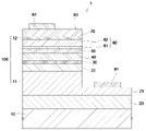
- FIG. 1 is a schematic cross-sectional view showing the configuration of a light emitting device according to one embodiment of the present invention.
- FIG. 2 is a flow chart showing the flow of the method for manufacturing a light emitting device according to one embodiment of the present invention.
- FIG. 3A is a schematic diagram showing a method for manufacturing a light emitting device according to one embodiment of the present invention.
- FIG. 3B is a schematic diagram showing a method for manufacturing a light emitting device according to one embodiment of the present invention.
- FIG. 3C is a schematic diagram showing a method for manufacturing a light emitting device according to one embodiment of the present invention;
- FIG. 1 is a schematic cross-sectional view of a light-emitting device 1 according to one embodiment of the present invention.
- the light emitting device 1 of this embodiment includes a first n-side semiconductor layer 20, a first p-side semiconductor layer 40, and a first active layer 30 provided between the first n-side semiconductor layer 20 and the first p-side semiconductor layer 40.
- the light emitting device 1 has an n-side electrode 91 electrically connected to the first n-side semiconductor layer 20 and a p-side electrode 92 electrically connected to the second p-side semiconductor layer 80 .
- the material of the substrate 10 is, for example, sapphire, silicon, SiC, GaN, or the like.
- a buffer layer may be provided between the substrate 10 and the first light emitting section 11 .
- As the buffer layer for example, a layer made of AlGaN or AlN can be used.
- the semiconductor laminate 100 is a laminate in which a plurality of semiconductor layers made of nitride semiconductors are laminated.
- the nitride semiconductor has a chemical formula of In x Al y Ga 1-x-y N (0 ⁇ x ⁇ 1, 0 ⁇ y ⁇ 1, x+y ⁇ 1), and the composition ratios x and y are varied within respective ranges. can include semiconductors of all compositions.
- the first light emitting section 11, the tunnel junction layer 50, and the second light emitting section 12 are arranged in this order from the substrate 10 side.
- the first light emitting unit 11 includes a first n-side semiconductor layer 20, a first p-side semiconductor layer 40, a first active layer 30 provided between the first n-side semiconductor layer 20 and the first p-side semiconductor layer 40, including.
- the first light emitting unit 11 is made of a nitride semiconductor.
- the first n-side semiconductor layer 20 includes an n-contact layer 21 , a first laminated portion 22 and an underlying layer 23 .
- the first n-side semiconductor layer 20 includes one or more n-type semiconductor layers.
- n-type semiconductor layers include semiconductor layers containing n-type impurities such as silicon (Si) and germanium (Ge).
- the n-type semiconductor layer is, for example, GaN, and may contain indium (In) and aluminum (Al).
- the n-type semiconductor layer containing Si as an n-type impurity has an n-type impurity concentration of 1 ⁇ 10 18 /cm 3 or more and 2 ⁇ 10 19 /cm 3 or less.
- the first n-side semiconductor layer 20 may include an undoped layer.
- An undoped layer is a layer that is not intentionally doped with n-type impurities or p-type impurities.
- the concentration of the n-type impurity and p-type impurity in the undoped layer is, for example, a concentration that does not exceed the detection limit in the analysis results of secondary ion mass spectrometry (SIMS) or the like.
- SIMS secondary ion mass spectrometry
- the undoped layer may contain n-type impurities and/or p-type impurities due to diffusion from the adjacent layers. May contain impurities.
- the n-contact layer 21 is provided between the underlying layer 23 and the first stacked portion 22 .
- the n-contact layer 21 is a semiconductor layer containing n-type impurities.
- the n-type impurity concentration of the n-contact layer 21 can be 1 ⁇ 10 18 /cm 3 or more and 1 ⁇ 10 19 /cm 3 or less.
- the thickness of the n-contact layer 21 can be 0.5 ⁇ m or more and 3 ⁇ m or less.
- the n-contact layer 21 has an upper surface on which no other semiconductor layer is provided.
- An n-side electrode 91 which will be described later, is provided on the surface of the n-contact layer 21 on which no other semiconductor layer is provided.
- the first laminated portion 22 is provided between the n-contact layer 21 and the first active layer 30 .
- the first laminated portion 22 has a multilayer structure in which first layers and second layers having a lattice constant different from that of the first layers are alternately laminated.
- the first laminated portion 22 is a superlattice layer including a plurality of first layers and a plurality of second layers.
- the first layer and the second layer are, for example, undoped layers.
- the first layer is, for example, an undoped GaN layer.
- the second layer is, for example, an undoped InGaN layer.
- the first laminated portion 22 includes, for example, 15 or more and 25 or less pairs of the first layer and the second layer.
- the thickness of the first layer can be 0.5 nm or more and 3 nm or less.
- the thickness of the second layer can be 0.5 nm or more and 3 nm or less.
- the thickness of the first laminated portion 22 can be, for example, 30 nm or more and 150 nm or less.
- the first n-type impurity concentration of the first stacked portion 22 can be, for example, 1 ⁇ 10 17 /cm 3 or more and 1 ⁇ 10 19 /cm 3 or less.
- the p-type impurity concentration of the first stacked portion 22 can be, for example, 1 ⁇ 10 17 /cm 3 or more and 1 ⁇ 10 18 /cm 3 or less.
- the first n-type impurity concentration of the first stacked portion 22 is the highest n-type impurity concentration among the n-type impurity concentrations in the first stacked portion 22 .
- the p-type impurity concentration of the first stacked portion 22 is the highest p-type impurity concentration among the p-type impurity concentrations in the first stacked portion 22 .
- the n-type impurity and the p-type impurity contained in the first stacked portion 22 are contained by being diffused from adjacent layers, the n-type impurity or the p-type impurity is added to the first layer and/or the second layer. Including cases where it is included by doping.
- the underlying layer 23 is provided between the substrate 10 and the n-contact layer 21 .
- the underlying layer 23 is, for example, an undoped GaN layer.
- the thickness of the underlying layer 23 can be, for example, 5 ⁇ m or more and 10 ⁇ m or less.
- the first active layer 30 is provided between the first n-side semiconductor layer 20 and the first p-side semiconductor layer 40 .
- the first active layer 30 has, for example, a multiple quantum well structure including multiple well layers and multiple barrier layers.
- InGaN for example, is used for the plurality of well layers.
- GaN is used for the plurality of barrier layers.
- the well layers and barrier layers included in the first active layer 30 are, for example, undoped layers. At least part of the well layers and barrier layers included in the first active layer 30 may contain n-type impurities and/or p-type impurities.
- the light emitted by the first active layer 30 is, for example, ultraviolet light or visible light.
- the first active layer 30 can emit blue light or green light, for example.
- the emission peak wavelength of blue light is 430 nm or more and 490 nm or less.
- the emission peak wavelength of green light is 500 nm or more and 540 nm or less.
- the first p-side semiconductor layer 40 is provided between the first active layer 30 and the tunnel junction layer 50 .
- the first p-side semiconductor layer 40 includes one or more p-type semiconductor layers.
- the p-type semiconductor layer include semiconductor layers containing p-type impurities such as magnesium (Mg).
- the p-type semiconductor layer is, for example, GaN and may contain In and/or Al.
- the p-type impurity concentration of the p-type semiconductor layer containing Mg as the p-type impurity is 1 ⁇ 10 19 /cm 3 or more and 5 ⁇ 10 20 /cm 3 or less.
- the first p-side semiconductor layer 40 may include an undoped layer.
- the thickness of the first p-side semiconductor layer 40 can be 30 nm or more and 200 nm or less.
- the tunnel junction layer 50 is provided between the first p-side semiconductor layer 40 and the second n-side semiconductor layer 60 .
- the tunnel junction layer 50 contains n-type impurities and/or p-type impurities.
- the tunnel junction layer 50 is at least one of a p-type semiconductor layer having a p-type impurity concentration higher than that of the first p-side semiconductor layer 40 and an n-type semiconductor layer having an n-type impurity concentration higher than that of the second n-side semiconductor layer 60. contains one semiconductor layer.
- the tunnel junction layer 50 includes, for example, a semiconductor layer with a third n-type impurity concentration higher than the second n-type impurity concentration of the second n-side semiconductor layer 60 .
- the width of a depletion layer formed by a pn junction can be made narrower.
- a p-type GaN layer containing Mg as a p-type impurity or an n-type GaN layer containing Si as an n-type impurity can be used.
- the p-type semiconductor layer containing Mg as a p-type impurity has a p-type impurity concentration of 1 ⁇ 10 20 /cm 3 or more and 5 ⁇ 10 21 /cm 3 or less.
- the n-type semiconductor layer containing Si as an n-type impurity has an n-type impurity concentration of 2 ⁇ 10 20 /cm 3 or more and 1 ⁇ 10 21 /cm 3 or less.
- Nitride semiconductors forming the tunnel junction layer 50 include, for example, GaN, InGaN, and AlGaN.
- the impurity concentration and thickness of the tunnel junction layer 50 can be changed as appropriate.
- the thickness of the tunnel junction layer 50 can be, for example, 1 nm or more and 6 ⁇ m or less.
- the second n-side semiconductor layer 60 includes an intermediate layer 61 and a second lamination portion 62 .
- the second n-side semiconductor layer 60 includes one or more n-type semiconductor layers.
- n-type semiconductor layers include semiconductor layers containing n-type impurities such as silicon (Si) and germanium (Ge).
- the n-type semiconductor layer is, for example, GaN, and may contain indium (In) and aluminum (Al).
- the n-type semiconductor layer containing Si as an n-type impurity has an n-type impurity concentration of 1 ⁇ 10 18 /cm 3 or more and 2 ⁇ 10 19 /cm 3 or less.
- the second n-side semiconductor layer 60 may include an undoped layer.
- the intermediate layer 61 is provided between the tunnel junction layer 50 and the second laminated section 62 .
- Intermediate layer 61 includes an n-type semiconductor layer containing n-type impurities.
- the intermediate layer 61 is formed by laminating a first n-type semiconductor layer and a second n-type semiconductor layer having a lower n-type impurity concentration than the first n-type semiconductor layer in this order from the tunnel junction layer 50 side. It can be a multi-layer structure.
- the n-type impurity concentration of the n-type semiconductor layer included in the intermediate layer 61 can be made lower than that of the n-type semiconductor layer included in the tunnel junction layer 50 .
- the surface condition of the semiconductor layers forming the second stacked portion 62 can be improved compared to the surface condition of the tunnel junction layer 50, so that the second stacked portion 62 can be formed with better crystallinity.
- the thickness of the intermediate layer 61 can be, for example, 100 nm or more and 200 ⁇ m or less.
- the thickness of the first n-type semiconductor layer can be set to 15 nm or more and 60 nm or less
- the thickness of the second n-type semiconductor layer can be set to 40 nm or more and 180 nm or less.
- the second lamination part 62 is provided between the intermediate layer 61 and the second active layer 70 .
- the second laminated portion 62 has a multilayer structure in which third layers and fourth layers having a lattice constant different from that of the third layers are alternately laminated.
- the second laminated portion 62 is a superlattice layer including a plurality of third layers and a plurality of fourth layers.
- the third layer and the fourth layer are layers doped with n-type impurities, for example.
- the third layer is, for example, an n-type GaN layer containing n-type impurities.
- the fourth layer is, for example, an n-type InGaN layer containing n-type impurities.
- the second laminated portion 62 includes, for example, 15 or more and 25 or less sets of the third layer and the fourth layer.
- the n-type impurity may be contained in either the third layer or the fourth layer.
- the third layer can be a layer doped with an n-type impurity
- the fourth layer can be an undoped layer.
- the thickness of the second laminated portion 62 can be made thinner than the thickness of the first laminated portion 22 . As a result, the expansion of the V pit formed on the upper surface of the second lamination portion 62 is suppressed more than that of the first lamination portion 22, and the crystallinity of the second active layer 70 formed on the second lamination portion 62 is improved. can do.
- the thickness of the third layer can be 0.5 nm or more and 3 nm or less.
- the thickness of the fourth layer can be 0.5 nm or more and 3 nm or less.
- the thickness of the second laminated portion 62 can be, for example, 30 nm or more and 150 nm or less.
- the thickness of the second lamination part 62 is thinner than that of the first lamination part 22, for example, the thickness of the first lamination part 22 is 50 nm or more and 70 nm or less, and the thickness of the second lamination part 62 is 30 nm or more and 50 nm or less.
- the second stacked portion 62 includes a semiconductor layer doped with n-type impurities.
- the second n-type impurity concentration of the second stacked portion 62 is higher than the first n-type impurity concentration of the first stacked portion 22 .
- diffusion of p-type impurities from the first p-side semiconductor layer 40 and the tunnel junction layer 50 into the semiconductor layer formed on the second stacked portion 62 can be suppressed.
- the second n-side semiconductor layer 60 contains a p-type impurity, there is a possibility that conversion to p-type is likely to be promoted.
- the semiconductor layer is less likely to become p-type due to the diffusion of such p-type impurities, and carriers can be efficiently supplied to the tunnel junction layer 50, so that the forward voltage Vf can be reduced.
- the second n-type impurity concentration of the second stacked portion 62 is, for example, preferably 3 ⁇ 10 17 /cm 3 or more and 1 ⁇ 10 20 /cm 3 or less, and 1 ⁇ 10 18 /cm 3 or more and 1 ⁇ 10 20 /cm 3 or more. cm 3 or less is more preferable.
- the p-type impurity concentration of the second stacked portion 62 is higher than the p-type impurity concentration of the first stacked portion 22 .
- the p-type impurity concentration of the second stacked portion 62 can be, for example, 3 ⁇ 10 17 /cm 3 or more and 5 ⁇ 10 18 /cm 3 or less.
- the second n-type impurity concentration of the second stacked portion 62 is the highest n-type impurity concentration among the n-type impurity concentrations in the second stacked portion 62 .
- the p-type impurity concentration of the second stacked portion 62 is the highest p-type impurity concentration among the p-type impurity concentrations in the second stacked portion 62 .
- the second n-type impurity concentration of the second stacked portion 62 is higher than the p-type impurity concentration of the second stacked portion 62 . Thereby, the second stacked portion 62 can be prevented from becoming p-type. For example, even if the p-type impurity concentration of the second stacked portion 62 is higher than the p-type impurity concentration of the first stacked portion 22, the second stacked portion 62 can be prevented from becoming p-type.
- the second active layer 70 is provided between the second laminated portion 62 and the second p-side semiconductor layer 80 .
- the second active layer 70 has, for example, a multiple quantum well structure including multiple well layers and multiple barrier layers.
- InGaN for example, is used for the plurality of well layers.
- GaN is used for the plurality of barrier layers.
- the well layers and barrier layers included in the second active layer 70 are, for example, undoped layers. At least part of the well layers and barrier layers included in the second active layer 70 may contain n-type impurities and/or p-type impurities.
- the light emitted by the second active layer 70 is, for example, ultraviolet light or visible light.
- the light emitted by the first active layer 30 and the second active layer 70 can be blue light, for example.
- the emission peak wavelength of the first active layer 30 and the emission peak wavelength of the second active layer 70 may be different.
- the light emitted by the first active layer 30 can be blue light
- the light emitted by the second active layer 70 can be green light.
- a second p-side semiconductor layer 80 is provided on the second active layer 70 .
- the second p-side semiconductor layer 80 includes one or more p-type semiconductor layers.
- the p-type semiconductor layer include semiconductor layers containing p-type impurities such as magnesium (Mg).
- the p-type semiconductor layer is, for example, GaN and may contain In and/or Al.
- the p-type impurity concentration of the p-type semiconductor layer containing Mg as the p-type impurity is 1 ⁇ 10 19 /cm 3 or more and 5 ⁇ 10 20 /cm 3 or less.
- the second p-side semiconductor layer 80 may include an undoped layer.
- the thickness of the second p-side semiconductor layer 80 can be 30 nm or more and 200 nm or less.
- the n-side electrode 91 is provided on the first n-side semiconductor layer 20 and electrically connected to the first n-side semiconductor layer.
- the n-side electrode 91 is provided on the upper surface of the n-contact layer 21 .
- the p-side electrode 92 is provided on the second p-side semiconductor layer 80 and electrically connected to the second p-side semiconductor layer 80 .
- a forward voltage is applied between the n-side electrode 91 and the p-side electrode 92 .
- a forward voltage is applied between the second p-side semiconductor layer 80 and the n-contact layer 21, and holes and electrons are supplied to the first active layer 30 and the second active layer 70, whereby the first The active layer 30 and the second active layer 70 emit light.
- the tunnel junction layer 50 is composed of a p-type semiconductor layer having a p-type impurity concentration higher than that of the first p-side semiconductor layer 40 and an n-type impurity concentration higher than that of the second n-side semiconductor layer 60. At least one of the n-type semiconductor layers is formed. A pn junction is formed by such a tunnel junction layer 50 .
- a pn junction is formed by the first p-side semiconductor layer 40 and the tunnel junction layer 50 using an n-type semiconductor layer heavily doped with n-type impurities.
- a pn junction is formed by the tunnel junction layer 50 using a p-type semiconductor layer heavily doped with p-type impurities and the second n-side semiconductor layer 60 .
- the tunnel junction layer 50 by forming the tunnel junction layer 50 into a stacked structure including an n-type semiconductor layer heavily doped with an n-type impurity and a p-type semiconductor layer heavily doped with a p-type impurity, a pn junction is formed. Form. The higher the concentration of each conductivity type impurity contained in the first p-side semiconductor layer 40, the tunnel junction layer 50, and the second n-side semiconductor layer 60, the narrower the width of the depletion layer formed by the above-described pn junction. .
- the light emitting device of the present embodiment diffusion of the p-type impurity into the second stacked portion 62 and the semiconductor layer formed on the second stacked portion 62 is suppressed, and the forward voltage Vf is reduced. can be reduced. Moreover, by laminating the second active layer 70 on the first active layer 30, the output per unit area can be increased compared to a light emitting device having one active layer.
- FIG. 2 is a flow chart showing the method for manufacturing the light emitting device of this embodiment.
- the method for manufacturing a light-emitting element of this embodiment includes a first light-emitting portion forming step S11, a tunnel junction layer forming step S12, and a second light-emitting portion forming step S13.
- 3A to 3C are schematic cross-sectional views showing the method for manufacturing the light emitting device 1 of this embodiment.
- Each nitride semiconductor layer included in the semiconductor laminate 100 is formed by MOCVD (metal organic chemical vapor deposition) in a furnace in which pressure and temperature can be adjusted. Each nitride semiconductor layer is epitaxially grown on the substrate 10, for example.
- Each nitride semiconductor layer can be formed by introducing a carrier gas and a source gas into a furnace. Hydrogen (H 2 ) gas or nitrogen (N 2 ) gas can be used as the carrier gas. Ammonia (NH 3 ) gas can be used as the raw material gas for the N source.
- As a material gas for the Ga source trimethylgallium (TMG) gas or triethylgallium (TEG) gas can be used.
- Trimethylindium (TMI) gas can be used as the material gas for the In source.
- Trimethylaluminum (TMA) gas can be used as the raw material gas for the Al source.
- Monosilane (SiH 4 ) gas can be used as the raw material gas for the Si source.
- Biscyclopentadienylmagnesium (Cp 2 Mg) gas can be used as the raw material gas for the Mg source.
- the first light emitting portion forming step S11 includes a step of forming the first n-side semiconductor layer 20 on the substrate 10, a step of forming the first active layer 30 on the first n-side semiconductor layer 20, and a step of forming the first active layer 30 on the first n-side semiconductor layer 20. and forming a first p-side semiconductor layer 40 thereon.
- the step of forming the first n-side semiconductor layer 20 the underlying layer 23, the n-contact layer 21, and the first stacked portion 22 are formed on the substrate 10 in this order. As shown in FIG.
- the first light emitting portion including the first n-side semiconductor layer 20, the first active layer 30, and the first p-side semiconductor layer 40 is formed on the substrate 10 by the first light emitting portion forming step S11. 11 is formed.
- a buffer layer may be formed on the surface of the substrate 10 before forming the underlying layer 23 on the substrate 10 .
- GaN or AlGaN can be used as the buffer layer.
- the first laminated portion 22 is formed, for example, by alternately performing a first layer forming process and a second layer forming process.
- a carrier gas and a raw material gas containing a Ga source and an N source are introduced into a furnace to form a first layer made of an undoped GaN layer.
- a carrier gas and a raw material gas containing a Ga source, an N source, and an In source are introduced into a furnace to form a second layer made of undoped InGaN.
- the first stacked portion 22 is formed so that the first n-type impurity concentration is, for example, 1 ⁇ 10 17 /cm 3 or more and 1 ⁇ 10 19 /cm 3 or less.
- a tunnel junction layer forming step S12 is performed.
- a tunnel junction layer 50 is formed on the first light emitting section 11, as shown in FIG. 3B.
- a tunnel junction made of a GaN layer having a third n-type impurity concentration is formed by introducing a carrier gas and a raw material gas containing a Ga source, an N source, and a Si source into a furnace.
- a layer 50 is formed.
- the tunnel junction layer 50 is adjusted such that the third n-type impurity concentration is 2 ⁇ 10 20 /cm 3 or more and 1 ⁇ 10 21 /cm 3 or less.
- the flow ratio of the Si raw material gas is set higher than the flow ratio of the Si raw material gas in the third layer forming process and the fourth layer forming process, which will be described later.
- the second light emitting portion forming step S13 is performed.
- the second light emitting portion 12 is formed on the tunnel junction layer 50, as shown in FIG. 3C.
- the second light emitting portion forming step S13 includes a step of forming the second n-side semiconductor layer 60 on the tunnel junction layer 50, a step of forming the second active layer 70 on the second n-side semiconductor layer 60, and a step of forming the second active layer 70 on the second n-side semiconductor layer 60. and forming a second p-side semiconductor layer 80 on 70 .
- the intermediate layer 61 and the second lamination portion 62 are formed on the tunnel junction layer 50 in this order.
- the intermediate layer 61 is formed in contact with the tunnel junction layer 50, for example.
- the second laminated portion 62 is formed, for example, by alternately performing a third layer forming process and a fourth layer forming process.
- a carrier gas and a material gas containing a Ga source, an N source, and a Si source are introduced into a furnace to form a GaN layer doped with n-type impurities.
- a carrier gas and a raw material gas containing a Ga source, an N source, an In source, and a Si source are introduced into the furnace to form a fourth layer of InGaN doped with n-type impurities.
- Form 4 layers for example, a carrier gas and a material gas containing a Ga source, an N source, an In source, and a Si source are introduced into the furnace to form a fourth layer of InGaN doped with n-type impurities.
- the second stacked portion 62 is adjusted so that the concentration of the second n-type impurity in the second stacked portion 62 becomes It is formed so as to be higher than the first n-type impurity concentration in the first stacked portion 22 .
- the second stacked portion 62 is formed so that the second n-type impurity concentration is, for example, 3 ⁇ 10 17 /cm 3 or more and 1 ⁇ 10 20 /cm 3 or less.
- part of the semiconductor stack 100 is removed to expose part of the n-contact layer 21 .
- an n-side electrode 91 is formed on the n-contact layer 21 and a p-side electrode 92 is formed on the second p-side semiconductor layer 80 .
- the n-side electrode 91 and the p-side electrode 92 can be formed by, for example, a sputtering method or a vapor deposition method. Through these steps, the light emitting device 1 shown in FIG. 1 can be obtained.
- the light-emitting element of the example and the light-emitting element of the comparative example were produced as follows, and the values of the forward voltage Vf and the output Po of the light-emitting element of the example and the light-emitting element of the comparative example were evaluated.
- a sapphire substrate was used as the substrate 10 .
- a buffer layer composed of an undoped AlGaN layer was formed on the sapphire substrate.
- an underlayer 23 of undoped GaN layer having a thickness of about 7 ⁇ m was formed on the buffer layer.
- An Si-doped n-contact layer 21 having a thickness of about 1.8 ⁇ m was formed on the underlying layer 23 .
- the n-type impurity concentration of the n-contact layer 21 is approximately 1 ⁇ 10 19 /cm 3 .
- a first laminated portion 22 was formed by alternately laminating a first layer made of an undoped GaN layer and a second layer made of an undoped InGaN layer.
- the thickness of the first layer was about 2 nm, and the thickness of the second layer was about 1 nm.
- the first laminated portion 22 includes 20 pairs of the first layer and the second layer.
- the n-type impurity concentration in the first stacked portion 22 is approximately 3 ⁇ 10 17 /cm 3 .
- Undoped InGaN layers and undoped GaN layers were alternately laminated as the first active layer 30 on the first lamination portion 22 to form seven sets of undoped InGaN layers and undoped GaN layers.
- An Mg-doped AlGaN layer, an undoped GaN layer, and an Mg-doped GaN layer were sequentially formed on the first active layer 30 as the first p-side semiconductor layer 40 .
- the p-type impurity concentration of the Mg-doped GaN layer in the first p-side semiconductor layer 40 is approximately 3 ⁇ 10 20 /cm 3 .
- a Si-doped GaN layer was formed as the tunnel junction layer 50 on the first p-side semiconductor layer 40 .
- the n-type impurity concentration of the tunnel junction layer 50 is approximately 8 ⁇ 10 20 /cm 3 .
- the thickness of the tunnel junction layer 50 was set to approximately 2 nm.
- a Si-doped GaN layer was formed as an intermediate layer 61 on the tunnel junction layer 50 .
- the n-type impurity concentration of the intermediate layer 61 is approximately 8 ⁇ 10 20 /cm 3 .
- the thickness of the intermediate layer 61 was set to approximately 145 nm.
- a second laminated portion 62 was formed on the intermediate layer 61 as a second laminated portion 62 by alternately laminating a third layer made of a Si-doped GaN layer and a fourth layer made of a Si-doped InGaN layer.
- the film thickness of the third layer was about 2 nm, and the film thickness of the fourth layer was about 1 nm.
- the second laminated portion 62 includes 20 pairs of the third layer and the fourth layer.
- the n-type impurity concentration in the second stacked portion 62 is approximately 2 ⁇ 10 19 /cm 3 .
- Undoped InGaN layers and undoped GaN layers were alternately laminated as the second active layer 70 on the second lamination portion 62 to form seven sets of undoped InGaN layers and undoped GaN layers.
- An Mg-doped AlGaN layer, an undoped GaN layer, and an Mg-doped GaN layer were sequentially formed on the second active layer 70 as the second p-side semiconductor layer 80 .
- the p-type impurity concentration of the Mg-doped GaN layer in the second p-side semiconductor layer 80 is approximately 3 ⁇ 10 20 /cm 3 .
- a light-emitting device having such a semiconductor laminate 100 was produced as an example.
- the light-emitting device of the comparative example has the same structure as the light-emitting device of the example except that the structure of the second lamination portion 62 is different.
- the second laminated portion 62 has a structure in which 20 sets of third layers made of undoped InGaN layers and fourth layers made of undoped GaN layers are alternately laminated. That is, the third layer and the fourth layer of the second lamination part 62 in the light emitting device of the comparative example were formed without doping the n-type impurity.
- the forward voltage Vf of the light emitting element of Example was 0.13 V lower than the forward voltage Vf of the light emitting element of Comparative Example. Moreover, the output Po of the light emitting element of the example was substantially the same as the output Po of the light emitting element of the comparative example. Note that the value of the forward voltage Vf is the value when a current of 500 mA is applied to the light emitting element. From these evaluation results, it was confirmed that the light emitting device of the example can reduce the forward voltage Vf more than the light emitting device of the comparative example while maintaining the output Po.
Abstract
Description
基板10にはサファイア基板を用いた。そのサファイア基板上に、アンドープのAlGaN層からなるバッファ層を形成した。バッファ層上に、アンドープのGaN層からなる厚さ約7μmの下地層23を形成した。下地層23上に、Siをドープした厚さ約1.8μmのnコンタクト層21を形成した。nコンタクト層21のn型不純物濃度は、1×10¹⁹/cm3程度である。nコンタクト層21上に、アンドープのGaN層からなる第1層と、アンドープのInGaN層からなる第2層を交互に積層した第1積層部22を形成した。第1層の膜厚は約2nmとし、第2層の膜厚は約1nmとした。第1積層部22は、第1層と第2層の組を20組含む。第1積層部22におけるn型不純物濃度は、3×1017/cm3程度である。第1積層部22上に、第1活性層30として、アンドープのInGaN層とアンドープのGaN層とを交互に積層し、アンドープのInGaN層とアンドープのGaN層との組を7組形成した。第1活性層30上に、第1p側半導体層40として、MgをドープしたAlGaN層、アンドープのGaN層、およびMgをドープしたGaN層を順に形成した。第1p側半導体層40におけるMgをドープしたGaN層のp型不純物濃度は、3×1020/cm3程度である。
トンネル接合層50の厚さは、約2nmとした。
比較例の発光素子は、第2積層部62の構造が異なっている以外は実施例の発光素子と同じ構造である。具体的には、第2積層部62を、アンドープのInGaN層からなる第3層と、アンドープのGaN層からなる第4層とを交互に20組積層した構造とした。つまり、比較例の発光素子における第2積層部62の第3層及び第4層は、n型不純物をドープせずに形成した。
10 基板
11 第1発光部
12 第2発光部
20 第1n側半導体層
21 nコンタクト層
22 第1積層部
23 下地層
30 第1活性層
40 第1p側半導体層
50 トンネル接合層
60 第2n側半導体層
61 中間層
62 第2積層部
70 第2活性層
80 第2p側半導体層
91 n側電極
92 p側電極
100 半導体積層体
Claims (7)
- 第1n側半導体層と、第1p側半導体層と、前記第1n側半導体層と前記第1p側半導体層との間に設けられた第1活性層と、を含む窒化物半導体からなる第1発光部と、第1発光部上に位置し、第2n側半導体層と、第2p側半導体層と、前記第2n側半導体層と前記第2p側半導体層との間に設けられた第2活性層と、を含む窒化物半導体からなる第2発光部と、前記第1p側半導体層と前記第2n側半導体層との間に設けられたトンネル接合層と、を有する半導体積層体と、
前記第1n側半導体層に電気的に接続されたn側電極と、
前記第2p側半導体層に電気的に接続されたp側電極と、を有し、
前記第1n側半導体層は、第1層と、前記第1層とは異なる格子定数である第2層と、が交互に積層された多層構造を有する第1n型不純物濃度の第1積層部を含み、
前記第2n側半導体層は、第3層と、前記第3層とは異なる格子定数である第4層と、が交互に積層された多層構造を有する第2n型不純物濃度の第2積層部を含み、
前記第2n型不純物濃度は、前記第1n型不純物濃度よりも高い発光素子。 - 前記第2積層部の厚さは、前記第1積層部の厚さよりも薄い請求項1に記載の発光素子。
- 前記第1層及び前記第2層は、アンドープの層である請求項1又は2に記載の発光素子。
- 前記第3層及び前記第4層は、n型不純物がドープされた層である請求項1から3のいずれか一項に記載の発光素子。
- 前記トンネル接合層は、前記第2n型不純物濃度よりも高い第3n型不純物濃度の半導体層を含む請求項1から4のいずれか一項に記載の発光素子。
- 前記第2n型不純物濃度は、前記第2積層部のp型不純物濃度よりも高い請求項1から5のいずれか一項に記載の発光素子。
- 前記第2積層部のp型不純物濃度は、前記第1積層部のp型不純物濃度よりも高い請求項1から6のいずれか一項に記載の発光素子。
Priority Applications (5)
| Application Number | Priority Date | Filing Date | Title |
|---|---|---|---|
| US18/261,439 US20240072209A1 (en) | 2021-03-18 | 2022-03-03 | Light-emitting element |
| KR1020237029378A KR20230157953A (ko) | 2021-03-18 | 2022-03-03 | 발광 소자 |
| EP22771128.0A EP4310926A1 (en) | 2021-03-18 | 2022-03-03 | Light-emitting element |
| JP2023506960A JPWO2022196374A1 (ja) | 2021-03-18 | 2022-03-03 | |
| CN202280021530.7A CN117015860A (zh) | 2021-03-18 | 2022-03-03 | 发光元件 |
Applications Claiming Priority (2)
| Application Number | Priority Date | Filing Date | Title |
|---|---|---|---|
| JP2021045210 | 2021-03-18 | ||
| JP2021-045210 | 2021-03-18 |
Publications (1)
| Publication Number | Publication Date |
|---|---|
| WO2022196374A1 true WO2022196374A1 (ja) | 2022-09-22 |
Family
ID=83322280
Family Applications (1)
| Application Number | Title | Priority Date | Filing Date |
|---|---|---|---|
| PCT/JP2022/009141 WO2022196374A1 (ja) | 2021-03-18 | 2022-03-03 | 発光素子 |
Country Status (6)
| Country | Link |
|---|---|
| US (1) | US20240072209A1 (ja) |
| EP (1) | EP4310926A1 (ja) |
| JP (1) | JPWO2022196374A1 (ja) |
| KR (1) | KR20230157953A (ja) |
| CN (1) | CN117015860A (ja) |
| WO (1) | WO2022196374A1 (ja) |
Citations (6)
| Publication number | Priority date | Publication date | Assignee | Title |
|---|---|---|---|---|
| JP2010016079A (ja) * | 2008-07-02 | 2010-01-21 | Toyoda Gosei Co Ltd | 発光素子、および発光素子の製造方法 |
| JP2010539731A (ja) * | 2007-09-19 | 2010-12-16 | ザ リージェンツ オブ ザ ユニバーシティ オブ カリフォルニア | パターン化した基板上の(Al,In,Ga,B)N装置 |
| US20150060877A1 (en) * | 2013-08-30 | 2015-03-05 | Epistar Corporation | Optoelectronic semiconductor device with barrier layer |
| JP2017157667A (ja) | 2016-03-01 | 2017-09-07 | 学校法人 名城大学 | 窒化物半導体発光素子 |
| JP2018201009A (ja) * | 2017-05-25 | 2018-12-20 | 昭和電工株式会社 | 発光ダイオードおよびトンネル接合層の製造方法 |
| JP2019517144A (ja) * | 2016-05-20 | 2019-06-20 | ルミレッズ リミテッド ライアビリティ カンパニー | 発光デバイスのp型層を形成する方法 |
-
2022
- 2022-03-03 JP JP2023506960A patent/JPWO2022196374A1/ja active Pending
- 2022-03-03 US US18/261,439 patent/US20240072209A1/en active Pending
- 2022-03-03 CN CN202280021530.7A patent/CN117015860A/zh active Pending
- 2022-03-03 KR KR1020237029378A patent/KR20230157953A/ko unknown
- 2022-03-03 EP EP22771128.0A patent/EP4310926A1/en active Pending
- 2022-03-03 WO PCT/JP2022/009141 patent/WO2022196374A1/ja active Application Filing
Patent Citations (6)
| Publication number | Priority date | Publication date | Assignee | Title |
|---|---|---|---|---|
| JP2010539731A (ja) * | 2007-09-19 | 2010-12-16 | ザ リージェンツ オブ ザ ユニバーシティ オブ カリフォルニア | パターン化した基板上の(Al,In,Ga,B)N装置 |
| JP2010016079A (ja) * | 2008-07-02 | 2010-01-21 | Toyoda Gosei Co Ltd | 発光素子、および発光素子の製造方法 |
| US20150060877A1 (en) * | 2013-08-30 | 2015-03-05 | Epistar Corporation | Optoelectronic semiconductor device with barrier layer |
| JP2017157667A (ja) | 2016-03-01 | 2017-09-07 | 学校法人 名城大学 | 窒化物半導体発光素子 |
| JP2019517144A (ja) * | 2016-05-20 | 2019-06-20 | ルミレッズ リミテッド ライアビリティ カンパニー | 発光デバイスのp型層を形成する方法 |
| JP2018201009A (ja) * | 2017-05-25 | 2018-12-20 | 昭和電工株式会社 | 発光ダイオードおよびトンネル接合層の製造方法 |
Also Published As
| Publication number | Publication date |
|---|---|
| EP4310926A1 (en) | 2024-01-24 |
| CN117015860A (zh) | 2023-11-07 |
| US20240072209A1 (en) | 2024-02-29 |
| KR20230157953A (ko) | 2023-11-17 |
| JPWO2022196374A1 (ja) | 2022-09-22 |
Similar Documents
| Publication | Publication Date | Title |
|---|---|---|
| JP5737111B2 (ja) | Iii族窒化物半導体発光素子 | |
| WO2016125492A1 (ja) | Iii族窒化物半導体発光素子およびその製造方法 | |
| US7759694B2 (en) | Nitride semiconductor light-emitting device | |
| US11569413B2 (en) | Method for manufacturing light-emitting element | |
| KR100784065B1 (ko) | 질화물 반도체 발광소자 및 그 제조방법 | |
| JP2007088270A (ja) | 半導体発光素子およびそれを用いる照明装置ならびに半導体発光素子の製造方法 | |
| JP2007150066A (ja) | 窒化物半導体発光素子 | |
| TWI416760B (zh) | 三族氮化物系化合物半導體發光元件及其製造方法 | |
| JP2007088269A (ja) | 半導体発光素子およびそれを用いる照明装置ならびに半導体発光素子の製造方法 | |
| US8659041B2 (en) | Nitride semiconductor light emitting diode | |
| JP2007299848A (ja) | 半導体発光素子 | |
| US20210305451A1 (en) | Method of manufacturing nitride semiconductor device | |
| US20090078961A1 (en) | Nitride-based light emitting device | |
| WO2022196374A1 (ja) | 発光素子 | |
| JP7149486B2 (ja) | 発光素子の製造方法 | |
| JP7344434B2 (ja) | 発光素子の製造方法 | |
| JP7385138B2 (ja) | 発光素子の製造方法 | |
| JP7432844B2 (ja) | 窒化物半導体発光素子 | |
| US20230170435A1 (en) | Light-emitting element and method for manufacturing the light-emitting element | |
| US20150243845A1 (en) | Light-emitting device | |
| JP2023091443A (ja) | 発光素子 | |
| JP4104686B2 (ja) | 半導体発光素子 | |
| JP2023091442A (ja) | 発光素子 | |
| JP2023080013A (ja) | 発光素子および発光素子の製造方法 | |
| JP2023184145A (ja) | 窒化物半導体発光素子 |
Legal Events
| Date | Code | Title | Description |
|---|---|---|---|
| 121 | Ep: the epo has been informed by wipo that ep was designated in this application |
Ref document number: 22771128 Country of ref document: EP Kind code of ref document: A1 |
|
| ENP | Entry into the national phase |
Ref document number: 2023506960 Country of ref document: JP Kind code of ref document: A |
|
| WWE | Wipo information: entry into national phase |
Ref document number: 18261439 Country of ref document: US |
|
| WWE | Wipo information: entry into national phase |
Ref document number: 202280021530.7 Country of ref document: CN |
|
| WWE | Wipo information: entry into national phase |
Ref document number: 2022771128 Country of ref document: EP |
|
| NENP | Non-entry into the national phase |
Ref country code: DE |
|
| ENP | Entry into the national phase |
Ref document number: 2022771128 Country of ref document: EP Effective date: 20231018 |