WO2022196262A1 - 電子部品内蔵基板及びその製造方法 - Google Patents
電子部品内蔵基板及びその製造方法 Download PDFInfo
- Publication number
- WO2022196262A1 WO2022196262A1 PCT/JP2022/007194 JP2022007194W WO2022196262A1 WO 2022196262 A1 WO2022196262 A1 WO 2022196262A1 JP 2022007194 W JP2022007194 W JP 2022007194W WO 2022196262 A1 WO2022196262 A1 WO 2022196262A1
- Authority
- WO
- WIPO (PCT)
- Prior art keywords
- conductor
- electronic component
- layers
- layer
- conductor layer
- Prior art date
- Legal status (The legal status is an assumption and is not a legal conclusion. Google has not performed a legal analysis and makes no representation as to the accuracy of the status listed.)
- Ceased
Links
Images








Classifications
-
- H—ELECTRICITY
- H05—ELECTRIC TECHNIQUES NOT OTHERWISE PROVIDED FOR
- H05K—PRINTED CIRCUITS; CASINGS OR CONSTRUCTIONAL DETAILS OF ELECTRIC APPARATUS; MANUFACTURE OF ASSEMBLAGES OF ELECTRICAL COMPONENTS
- H05K1/00—Printed circuits
- H05K1/02—Details
- H05K1/03—Use of materials for the substrate
-
- H—ELECTRICITY
- H05—ELECTRIC TECHNIQUES NOT OTHERWISE PROVIDED FOR
- H05K—PRINTED CIRCUITS; CASINGS OR CONSTRUCTIONAL DETAILS OF ELECTRIC APPARATUS; MANUFACTURE OF ASSEMBLAGES OF ELECTRICAL COMPONENTS
- H05K1/00—Printed circuits
- H05K1/18—Printed circuits structurally associated with non-printed electric components
- H05K1/182—Printed circuits structurally associated with non-printed electric components associated with components mounted in printed circuit boards [PCB], e.g. insert-mounted components [IMC]
- H05K1/185—Printed circuits structurally associated with non-printed electric components associated with components mounted in printed circuit boards [PCB], e.g. insert-mounted components [IMC] associated with components encapsulated in the insulating substrate of the PCBs; associated with components incorporated in internal layers of multilayer circuit boards
- H05K1/186—Printed circuits structurally associated with non-printed electric components associated with components mounted in printed circuit boards [PCB], e.g. insert-mounted components [IMC] associated with components encapsulated in the insulating substrate of the PCBs; associated with components incorporated in internal layers of multilayer circuit boards manufactured by mounting on or connecting to patterned circuits before or during embedding
-
- H—ELECTRICITY
- H05—ELECTRIC TECHNIQUES NOT OTHERWISE PROVIDED FOR
- H05K—PRINTED CIRCUITS; CASINGS OR CONSTRUCTIONAL DETAILS OF ELECTRIC APPARATUS; MANUFACTURE OF ASSEMBLAGES OF ELECTRICAL COMPONENTS
- H05K1/00—Printed circuits
- H05K1/02—Details
- H05K1/0296—Conductive pattern lay-out details not covered by sub groups H05K1/02 - H05K1/0295
- H05K1/0298—Multilayer circuits
-
- H—ELECTRICITY
- H05—ELECTRIC TECHNIQUES NOT OTHERWISE PROVIDED FOR
- H05K—PRINTED CIRCUITS; CASINGS OR CONSTRUCTIONAL DETAILS OF ELECTRIC APPARATUS; MANUFACTURE OF ASSEMBLAGES OF ELECTRICAL COMPONENTS
- H05K1/00—Printed circuits
- H05K1/18—Printed circuits structurally associated with non-printed electric components
- H05K1/182—Printed circuits structurally associated with non-printed electric components associated with components mounted in printed circuit boards [PCB], e.g. insert-mounted components [IMC]
-
- H—ELECTRICITY
- H05—ELECTRIC TECHNIQUES NOT OTHERWISE PROVIDED FOR
- H05K—PRINTED CIRCUITS; CASINGS OR CONSTRUCTIONAL DETAILS OF ELECTRIC APPARATUS; MANUFACTURE OF ASSEMBLAGES OF ELECTRICAL COMPONENTS
- H05K1/00—Printed circuits
- H05K1/18—Printed circuits structurally associated with non-printed electric components
- H05K1/182—Printed circuits structurally associated with non-printed electric components associated with components mounted in printed circuit boards [PCB], e.g. insert-mounted components [IMC]
- H05K1/185—Printed circuits structurally associated with non-printed electric components associated with components mounted in printed circuit boards [PCB], e.g. insert-mounted components [IMC] associated with components encapsulated in the insulating substrate of the PCBs; associated with components incorporated in internal layers of multilayer circuit boards
-
- H—ELECTRICITY
- H05—ELECTRIC TECHNIQUES NOT OTHERWISE PROVIDED FOR
- H05K—PRINTED CIRCUITS; CASINGS OR CONSTRUCTIONAL DETAILS OF ELECTRIC APPARATUS; MANUFACTURE OF ASSEMBLAGES OF ELECTRICAL COMPONENTS
- H05K1/00—Printed circuits
- H05K1/02—Details
- H05K1/03—Use of materials for the substrate
- H05K1/0313—Organic insulating material
- H05K1/0353—Organic insulating material consisting of two or more materials, e.g. two or more polymers, polymer + filler, + reinforcement
- H05K1/0366—Organic insulating material consisting of two or more materials, e.g. two or more polymers, polymer + filler, + reinforcement reinforced, e.g. by fibres, fabrics
-
- H—ELECTRICITY
- H05—ELECTRIC TECHNIQUES NOT OTHERWISE PROVIDED FOR
- H05K—PRINTED CIRCUITS; CASINGS OR CONSTRUCTIONAL DETAILS OF ELECTRIC APPARATUS; MANUFACTURE OF ASSEMBLAGES OF ELECTRICAL COMPONENTS
- H05K2201/00—Indexing scheme relating to printed circuits covered by H05K1/00
- H05K2201/02—Fillers; Particles; Fibers; Reinforcement materials
- H05K2201/0275—Fibers and reinforcement materials
- H05K2201/029—Woven fibrous reinforcement or textile
-
- H—ELECTRICITY
- H05—ELECTRIC TECHNIQUES NOT OTHERWISE PROVIDED FOR
- H05K—PRINTED CIRCUITS; CASINGS OR CONSTRUCTIONAL DETAILS OF ELECTRIC APPARATUS; MANUFACTURE OF ASSEMBLAGES OF ELECTRICAL COMPONENTS
- H05K3/00—Apparatus or processes for manufacturing printed circuits
- H05K3/46—Manufacturing multilayer circuits
- H05K3/4644—Manufacturing multilayer circuits by building the multilayer layer by layer, i.e. build-up multilayer circuits
Definitions
- the present invention relates to an electronic component embedded substrate and its manufacturing method, and more particularly to an electronic component embedded substrate having a multilayer wiring structure and its manufacturing method.
- Patent Document 1 discloses an electronic component built-in board having a multilayer wiring structure.
- the electronic component-embedded substrate disclosed in Patent Document 1 includes an insulating layer in which electronic components are embedded, a two-layer wiring layer provided on one surface side of the insulating layer in which electronic components are embedded, and electronic components. and two wiring layers provided on the other surface side of the buried insulating layer.
- the insulating layer positioned between the two wiring layers uses a core material such as glass cloth impregnated with a resin material, thereby ensuring the mechanical strength of the entire substrate.
- an object of the present invention is to provide an electronic component built-in board and a method of manufacturing the same in which the degree of freedom in designing the outermost conductor layer including terminal electrodes is increased.
- An electronic component-embedded substrate includes a plurality of conductor layers and a plurality of insulating layers positioned between two adjacent conductor layers among the plurality of conductor layers in a stacking direction, and the plurality of insulating layers are provided with an electronic component.
- the plurality of conductor layers comprising first, second and third conductor layers stacked on one surface side of the first insulating layer; It includes fourth, fifth and sixth conductor layers laminated on the other surface side, and the plurality of insulation layers includes a second insulation layer positioned between the first conductor layer and the second conductor layer, and a second insulation layer positioned between the first conductor layer and the second conductor layer.
- a third insulating layer positioned between the second conductor layer and the third conductor layer; a fourth insulating layer positioned between the fourth conductor layer and the fifth conductor layer; a fifth insulating layer positioned between the conductor layers, the first conductor layer including a plurality of terminal electrodes exposed on one surface side, and the sixth conductor layer including a plurality of terminal electrodes exposed on the other surface side;
- the third and fourth insulating layers are made of a core material impregnated with a resin material, and at least one of the second and fifth insulating layers is made of a resin material that does not contain a core material. It is characterized by
- the second and fifth insulating layers is made of a resin material that does not contain a core material, the diameter of via conductors formed in at least one of the second and fifth insulating layers is reduced. can do. As a result, even when a plurality of terminal electrodes with a narrow pitch are formed on the first or sixth conductor layer, it is possible to suppress the routing of wiring.
- both the second and fifth insulating layers may be made of a resin material that does not contain a core material. According to this, since the diameter of the via conductors formed in the second and fifth insulating layers can be reduced, even when a plurality of terminal electrodes with a narrow pitch are formed in the first and sixth conductive layers, It is possible to suppress the routing of wiring.
- the second and third conductor layers include a plurality of signal wiring patterns connected to electronic components
- the third insulating layer locally includes a non-core region that does not contain a core material.
- the material region overlaps the electronic component in plan view, and the plurality of signal wiring patterns included in the second conductor layer and the plurality of signal wiring patterns included in the third conductor layer pass through the coreless material region. They may be connected to each other through a plurality of via conductors. According to this, it is possible to reduce the diameter of a plurality of via conductors penetrating through the coreless material region.
- the first and third conductor layers include a plurality of signal wiring patterns connected to electronic components
- the third insulating layer has openings, and the openings overlap the electronic components in plan view.
- the plurality of signal wiring patterns included in the first conductor layer and the plurality of signal wiring patterns included in the third conductor layer are connected to each other through a plurality of via conductors penetrating through the openings. It doesn't matter if it's something. According to this, it is possible to reduce the diameter of the plurality of via conductors passing through the opening.
- a method of manufacturing an electronic component built-in substrate includes: a first insulating layer in which an electronic component is embedded; first and second conductor layers laminated on one surface side of the first insulating layer; third and fourth conductor layers laminated on the other surface side of one insulating layer; and a third insulating layer positioned between the third conductor layer and the fourth conductor layer and made of a core material in which the core material is impregnated with a resin material. and forming fifth and sixth conductor layers on the surfaces of the first and fourth conductor layers via the fourth and fifth insulation layers, respectively, and forming the fourth and fifth insulation layers At least one is made of a resin material that does not contain a core material.
- the fourth and fifth insulating layers is made of a resin material that does not contain a core material, the diameter of via conductors formed in at least one of the fourth and fifth insulating layers is reduced. can do. As a result, even when a plurality of terminal electrodes with a narrow pitch are formed on the fifth or sixth conductor layer, it is possible to suppress the routing of wiring.
- both the fourth and fifth insulating layers may be made of a resin material that does not contain a core material. According to this, since the diameter of the via conductors formed in the fourth and fifth insulating layers can be reduced, even when a plurality of terminal electrodes with a narrow pitch are formed in the fifth and sixth conductor layers, It is possible to suppress the routing of wiring.
- a method of manufacturing a substrate with built-in electronic components provides a method of manufacturing a plurality of signal wiring patterns contained in a first conductor layer and a plurality of signal wiring patterns contained in a second conductor layer in a second insulating layer.
- a step of connecting to each other through a plurality of via conductors penetrating through core-free regions that do not essentially contain a core may be provided. According to this, it is possible to reduce the diameter of a plurality of via conductors penetrating through the coreless material region.
- a plurality of signal wiring patterns included in the fifth conductor layer and a plurality of signal wiring patterns included in the second conductor layer are provided on the second insulating layer.
- the method may further include a step of connecting to each other through a plurality of via conductors penetrating through the openings. According to this, it is possible to reduce the diameter of the plurality of via conductors passing through the opening.
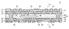
- FIG. 1 is a schematic cross-sectional view for explaining the structure of an electronic component built-in board 1 according to a first embodiment of the present invention.
- FIG. 2 is a process diagram for explaining the method of manufacturing the electronic component built-in substrate 1.
- FIG. 3 is a process chart for explaining the method of manufacturing the electronic component built-in substrate 1.
- FIG. 4 is a process chart for explaining the method of manufacturing the electronic component built-in substrate 1.
- FIG. 5 is a process diagram for explaining the method of manufacturing the electronic component built-in substrate 1.
- FIG. FIG. 6 is a process diagram for explaining the method of manufacturing the electronic component built-in substrate 1.
- FIG. FIG. FIG. 1 is a schematic cross-sectional view for explaining the structure of an electronic component built-in board 1 according to a first embodiment of the present invention.
- FIG. 2 is a process diagram for explaining the method of manufacturing the electronic component built-in substrate 1.
- FIG. 3 is a process chart for explaining the method of manufacturing the electronic component built-in substrate 1.
- FIG. 4 is
- FIG. 7 is a process diagram for explaining the method of manufacturing the electronic component built-in substrate 1.
- FIG. 8 is a process diagram for explaining the method of manufacturing the electronic component built-in substrate 1.
- FIG. 9 is a process diagram for explaining the method of manufacturing the electronic component built-in substrate 1.
- FIG. 10A to 10D are process diagrams for explaining the method of manufacturing the electronic component built-in substrate 1.
- FIG. 11 is a schematic cross-sectional view for explaining the structure of the electronic component built-in board 2 according to the second embodiment of the present invention.
- FIG. 12 is a schematic cross-sectional view for explaining the structure of the electronic component built-in board 3 according to the third embodiment of the present invention.
- FIG. 13A to 13D are process diagrams for explaining the method of manufacturing the electronic component built-in substrate 3.
- FIG. 14A to 14D are process diagrams for explaining a method of manufacturing the electronic component built-in board 3.
- FIG. 15A and 15B are process diagrams for explaining the method of manufacturing the electronic component built-in substrate 3.
- FIG. 16A to 16D are process diagrams for explaining the method of manufacturing the electronic component built-in board 3.
- FIG. 17 is a schematic cross-sectional view for explaining the structure of the electronic component built-in board 4 according to the fourth embodiment of the present invention.
- 18A to 18D are process diagrams for explaining the method of manufacturing the electronic component built-in board 4.
- FIG. 19A to 19D are process diagrams for explaining the method of manufacturing the electronic component built-in board 4.
- FIG. 20A to 20D are process diagrams for explaining the method of manufacturing the electronic component built-in board 4.
- FIG. 20A to 20D are process diagrams for explaining the method of manufacturing the electronic component built-in board 4.
- FIG. 1 is a schematic cross-sectional view for explaining the structure of an electronic component built-in board 1 according to a first embodiment of the present invention.
- the electronic component built-in substrate 1 includes six conductor layers L1 to L6 and insulating layers 11 to 15 respectively positioned between two adjacent conductor layers in the stacking direction.
- the insulating layer 11 is positioned between the conductor layers L1 and L2
- the insulating layer 12 is positioned between the conductive layers L2 and L3
- the insulating layer 13 is positioned between the conductive layers L3 and L4
- the insulating layer 14 is positioned between the conductor layers L3 and L4.
- Located between layers L4 and L5, insulating layer 15 is located between conductor layers L5 and L6.
- the insulating layers 11 to 15 are all interlayer films having conductor layers on the front and back surfaces, and in that sense the solder resists 21 and 22 do not correspond to insulating layers.
- the conductor layer L1 is located on the uppermost layer, and part of it is covered with a solder resist 21.
- the exposed portion of the conductor layer L1 that is not covered with the solder resist 21 constitutes the terminal electrode E1 located on the one surface 1a side of the substrate 1 with built-in electronic component.
- the conductor layer L6 is located at the bottom layer and is partially covered with the solder resist 22.
- the exposed portion of the conductor layer L6 that is not covered with the solder resist 22 constitutes the terminal electrode E2 located on the other surface 1b side of the electronic component built-in board 1.
- Electronic components such as a semiconductor IC and passive components (not shown) are mounted on the front surface 1a of the electronic component built-in substrate 1 .
- the surface 1b of the electronic component built-in substrate 1 is used as a mounting surface for another circuit board (not shown), or electronic components such as a semiconductor IC and passive components (not shown) are mounted.
- the insulating layers 12, 14, and 15 are made of a core material in which a core material such as glass fiber is impregnated with a resin material such as epoxy. Since the core material has high strength, the mechanical strength of electronic component built-in board 1 is mainly ensured by insulating layers 12 , 14 , 15 .
- the insulating layers 11 and 13 are made of a resin material that does not contain a core material such as glass cloth. A resin material that does not contain a core material, such as a glass cloth, is superior in workability compared to a core material, and can form small-diameter via holes at a narrow pitch.
- the insulating layer 13 is composed of two insulating layers 13a and 13b, and an electronic component 40 such as a semiconductor IC is embedded in the interface between the two layers.
- the electronic component 40 is mounted on the surface of the insulating layer 13a in a face-up manner so that the main surface 41 provided with the electrode pads faces the surface 1a.
- the thickness of the chip may be reduced to 200 ⁇ m or less, for example, about 50 to 100 ⁇ m.
- two conductor layers adjacent in the stacking direction are connected to each other by via conductors.
- the conductor layers L1 and L2 are connected through a via conductor 31 provided through the insulating layer 11, and the conductor layers L2 and L3 are connected through a via conductor 32 provided through the insulating layer 12.
- the conductor layers L3 and L4 are connected through via conductors 33 provided through the insulating layer 13, and the conductor layers L4 and L5 are connected through via conductors 34 provided through the insulating layer 14.
- the conductor layers L5 and L6 are connected through via conductors 35 provided through the insulating layer 15 .
- conductor layer L3 and electronic component 40 are connected through via conductors 36 provided through insulating layer 13b.
- the insulating layers 12, 14, 15 made of the core material and the insulating layers 11, 13 made of a resin material that does not contain a core material such as glass cloth are greatly different in workability. That is, since the insulating layers 11 and 13 made of a resin material are excellent in workability, small-diameter via holes can be easily formed, while the insulating layers 12, 14, and 15 made of a core material are made of a core material such as glass cloth. , it is difficult to form a small via hole. Therefore, via conductors 32 , 34 , 35 penetrating insulating layers 12 , 14 , 15 inevitably have larger diameters than via conductors 31 , 33 penetrating insulating layers 11 , 13 . As described above, it is difficult to form the via conductors 32 , 34 , 35 at a narrower pitch than the via conductors 31 , 33 .
- the uppermost conductor layer L1 is formed on the surface of the insulating layer 11 made of a resin material that does not contain a core material such as glass cloth, the small-diameter via conductors 31 can be formed narrowly. A large number of pitches can be formed. Therefore, even if the electrode pitch of the electronic components mounted on the one surface 1a is narrow, the routing of the wiring formed on the conductor layer L1 can be shortened, facilitating the layout design.
- the electronic component built-in substrate 1 has six conductor layers L1 to L6, so that more complicated wiring can be formed. Moreover, since the outermost insulating layer 11 located on the one surface 1a side is made of a resin material that does not contain a core material such as glass cloth, an electronic component with a narrow terminal pitch is mounted on the one surface 1a side. Layout design becomes easier even when This effect is due to the fact that the surface layer located on the circuit surface side of the built-in electronic component 40, that is, if the built-in electronic component 40 is of the face-up type, on the surface 1a side, there is an electronic device having wire bonding pads that require many terminals. It becomes conspicuous when parts are mounted.
- the insulating layers 12, 14 and 15 are made of a core material impregnated with a resin material, the mechanical strength of the electronic component built-in board 1 can be sufficiently ensured.
- the electronic component built-in substrate 1 may warp.
- the insulating layer 11 does not contain a core material and thus has a larger thermal expansion coefficient than the insulating layer 15 containing a core material.
- a resin material should be selected so that the coefficient of thermal expansion of the insulating layer 12 is smaller than the coefficient of thermal expansion of the insulating layers 14 and 15 .
- the insulating layer 12 may be thinner than the insulating layers 14 and 15 . As a result, the symmetry of the coefficient of thermal expansion in the stacking direction is enhanced, so that the electronic component built-in substrate 1 is less likely to warp.
- 2 to 10 are process diagrams for explaining the method of manufacturing the electronic component built-in substrate 1 according to this embodiment.
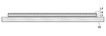
- a base material having conductor layers L4 and L5 made of Cu foil or the like formed on both sides of an insulating layer 14 made of a core material is prepared and fixed to a support 50.
- the conductor layer L4 having a desired pattern shape is completed by patterning the conductor layer L4 using a known technique such as photolithography.
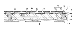
- an uncured (B-stage) resin sheet or the like is laminated on the surface of the insulating layer 14 by vacuum pressure bonding or the like so as to embed the patterned conductor layer L4. 13a.
- the electronic component 40 is placed on the surface of the insulating layer 13a. The electronic component 40 is mounted face-up so that the main surface 41 where the electrode pads are exposed faces upward.
- the insulating layer 13b and the conductor layer L3 are formed so as to cover the electronic component 40.
- the insulating layer 13b is formed, for example, by applying an uncured or semi-cured thermosetting resin, heating it to semi-cur it in the case of an uncured resin, and then using a pressing means to form the insulating layer 13b together with the conductor layer L3. Curing molding is preferred.
- the material used for the insulating layer 13b may be the same as that for the insulating layer 13a.
- the pad size of the embedded electronic component 40 is smaller than that of the terminal electrodes E1 and E2, and the pad pitch is required to be designed to be narrow. need to form small diameter vias. Considering this point, it is desirable to use a resin material that does not contain a core material, such as glass cloth, as the insulating layer 13b.
- via holes are formed in the insulating layer 13
- via conductors 33 and 36 are formed to fill the via holes
- the conductor layer L3 is patterned using a known technique such as photolithography.
- a conductor layer L3 having a desired pattern shape is completed.
- a portion of the conductor layer L3 is connected to the conductor layer L4 via the via conductors 33, and another portion of the conductor layer L3 is connected to the electronic component 40 via the via conductors .
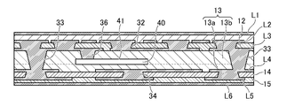
- the sheet in which the insulating layer 12 and the conductor layer L2 are laminated is vacuum hot pressed so as to embed the conductor layer L3.
- the material and thickness used for the insulating layer 12 may be the same as those for the insulating layer 14 .
- the support 50 is peeled off as shown in FIG.
- via conductors 32 and 34 are formed to fill the via holes.
- Conductive layers L2 and L5 having desired pattern shapes are completed by patterning L5.
- a portion of the conductor layer L2 is connected to the conductor layer L3 through the via conductors 32
- a portion of the conductor layer L5 is connected to the conductor layer L4 through the via conductors .
- the via holes are formed in the insulating layers 12 and 14, the diameter of the via holes is inevitably large because the core material existing at the positions must be removed. Accordingly, the diameters of the via conductors 32 and 34 also increase.
- a precursor of an electronic component built-in substrate having four conductor layers L2 to L5 is completed.
- a sheet in which the insulating layer 11 and the conductor layer L1 are laminated and a sheet in which the insulating layer 15 and the conductor layer L6 are laminated are prepared. are sandwiched and vacuum heat pressed. After forming via holes in the insulating layers 11 and 15, via conductors 31 and 35 are formed to fill the via holes. , 22, the electronic component built-in substrate 1 shown in FIG. 1 is completed.
- the insulating layer 11 does not contain a core material such as a glass cloth, in the step of forming via holes in the insulating layer 11, small-diameter via holes are formed at a narrow pitch by laser processing or blast processing. can be done. As a result, compared with the case where the core material is used as the material of the insulating layer 11, the degree of freedom in designing the layout of the conductor layer L1 is improved.
- FIG. 11 is a schematic cross-sectional view for explaining the structure of the electronic component built-in board 2 according to the second embodiment of the present invention.
- the insulation layer 15 located on the lowermost layer side is made of a resin material such as glass cloth that does not contain a core material, which is different from the first embodiment. It is different from the electronic component built-in board 1 according to the form. Since other basic configurations are the same as those of the electronic component built-in substrate 1 according to the first embodiment, the same elements are denoted by the same reference numerals, and overlapping descriptions are omitted.
- the conductor layer L6 located at the bottom layer is formed on the surface of the insulating layer 15 made of a resin material that does not contain a core material such as a glass cloth, the small-diameter via conductors 35 are arranged at a narrow pitch. Many can be formed. Therefore, layout design of the conductor layer L6 is facilitated even when the electrode pitch of the electronic components mounted not only on the one surface 1a side but also on the other surface 1b side is narrow.
- FIG. 12 is a schematic cross-sectional view for explaining the structure of the electronic component built-in board 3 according to the third embodiment of the present invention.
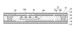
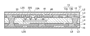
- the electronic component built-in substrate 3 according to the third embodiment is different from the second embodiment in that the non-core material region 12A that does not contain the core material is locally provided in the insulating layer 12. It is different from the electronic component built-in board 2 by . Since other basic configurations are the same as those of the electronic component built-in board 2 according to the second embodiment, the same elements are denoted by the same reference numerals, and overlapping descriptions are omitted.
- the non-core material region 12A is provided at a position overlapping the electronic component 40 in plan view, and the signal terminals of the electronic component 40 are included in the conductor layer L3 via the via conductors 36.
- the signal wiring pattern S3 of the conductor layer L3 is connected to the plurality of signal wiring patterns S2 included in the conductor layer L2 via the via conductors 32S.
- the signal wiring patterns S2 and S3 are connected to each other through a plurality of via conductors 32S penetrating through the coreless material region 12A.
- the diameter and pitch of the via conductors 32S formed in the coreless region 12A are different from those formed in other regions of the insulating layer 12. It can be made smaller than the diameter and pitch of the via conductors 32 .
- 13 to 16 are process diagrams for explaining the method of manufacturing the electronic component built-in substrate 3 according to this embodiment.
- a sheet in which the insulating layer 12 having the non-core material region 12A and the conductor layer L2 are laminated is vacuum hot pressed.
- the coreless material region 12A is positioned so as to overlap the signal wiring pattern S3 included in the conductor layer L3.
- the support 50 is peeled off.
- the non-core region 12A of the insulating layer 12 may be formed by punching with a mold press or by drilling, laser processing, or the like in an uncured state before vacuum hot pressing.
- via conductors 32 and 34 are formed to fill the via holes.
- Conductive layers L2 and L5 having desired pattern shapes are completed by patterning L5.
- the signal wiring pattern S3 included in the conductor layer L2 is connected to the signal wiring pattern S3 of the conductor layer L3 through the via conductors 32S.
- the precursor is sandwiched between a sheet in which the insulating layer 11 and the conductor layer L1 are laminated and a sheet in which the insulating layer 15 and the conductor layer L6 are laminated, and is vacuum hot pressed.
- the insulating layer 12 is provided with the non-core material region 12A that does not contain a core material such as a glass cloth, the mechanical strength of the insulating layer 12 is ensured while the via conductor 32S diameter and pitch can be reduced.
- FIG. 17 is a schematic cross-sectional view for explaining the structure of the electronic component built-in board 4 according to the fourth embodiment of the present invention.
- the electronic component built-in board 4 according to the fourth embodiment differs from the electronic component built-in board 2 according to the second embodiment in that the insulating layer 12 is provided with an opening 12B. Since other basic configurations are the same as those of the electronic component built-in board 2 according to the second embodiment, the same elements are denoted by the same reference numerals, and overlapping descriptions are omitted.
- an opening 12B is provided at a position overlapping the electronic component 40 in plan view.
- the opening 12B is a region where the insulating layer 12 is not present (removed), and the inside of the opening 12B is filled with the insulating layer 11 .
- the signal terminals of the electronic component 40 are connected to the plurality of signal wiring patterns S3 included in the conductor layer L3 through the via conductors 36, and the signal wiring patterns S3 of the conductor layer L3 are connected through the via conductors 31S. It is connected to a plurality of signal wiring patterns S1 included in the conductor layer L1.
- the signal wiring patterns S1 and S3 are connected to each other through a plurality of via conductors 31S penetrating through the opening 12B.
- the insulating layer 12 does not exist in the openings 12B, and the openings 12B are filled with the insulating layer 11. Therefore, the diameter and pitch of the via conductors 31S formed in the openings 12B are equal to those formed in the insulating layer 12. The diameter and pitch of the via conductors 32 can be reduced.
- the signal wiring patterns S2 and S3 are not detoured and are connected to the conductor layer L1 at the shortest distance. It becomes possible to Moreover, since the via conductor 31S directly connects the signal wiring patterns S1 and S3, the wiring distance between the electronic component 40 and the terminal electrode E1 is further shortened.
- 18 to 20 are process diagrams for explaining the method of manufacturing the electronic component built-in board 4 according to this embodiment.
- the conductor layers L2 and L5 having desired pattern shapes are completed by patterning the conductor layers L2 and L5 as shown in FIG.
- the conductor layer L2 on the insulating layer 12 is completely removed in the region where the opening 12B is to be formed.
- openings 12B are formed by partially removing the insulating layer 12 by well-known techniques such as drilling and laser processing.
- the precursor is sandwiched between a sheet in which the insulating layer 11 and the conductor layer L1 are laminated and a sheet in which the insulating layer 15 and the conductor layer L6 are laminated, and is vacuum hot pressed.
- the insulating layer 12 is provided with the openings 12B, it is possible to reduce the diameter and pitch of the via conductors 31S while ensuring the mechanical strength of the insulating layer 12. becomes.
- Electronic component built-in substrate 1a One surface 1b of electronic component built-in substrate The other surface 11-15, 13a, 13b of electronic component built-in substrate Insulating layer 12A Coreless material region 12B Openings 21, 22 Solder resists 31-36 , 31S, 32S via conductors 40 electronic component 41 main surface 50 of electronic component supports E1, E2 terminal electrodes L1 to L6 conductor layers S1 to S3 signal wiring pattern
Landscapes
- Engineering & Computer Science (AREA)
- Microelectronics & Electronic Packaging (AREA)
- Manufacturing & Machinery (AREA)
- Production Of Multi-Layered Print Wiring Board (AREA)
- Structure Of Printed Boards (AREA)
Abstract
Description
図1は、本発明の第1の実施形態による電子部品内蔵基板1の構造を説明するための模式的な断面図である。
図11は、本発明の第2の実施形態による電子部品内蔵基板2の構造を説明するための模式的な断面図である。
図12は、本発明の第3の実施形態による電子部品内蔵基板3の構造を説明するための模式的な断面図である。
図17は、本発明の第4の実施形態による電子部品内蔵基板4の構造を説明するための模式的な断面図である。
1a 電子部品内蔵基板の一方の表面
1b 電子部品内蔵基板の他方の表面
11~15,13a,13b 絶縁層
12A 無芯材領域
12B 開口部
21,22 ソルダーレジスト
31~36,31S,32S ビア導体
40 電子部品
41 電子部品の主面
50 支持体
E1,E2 端子電極
L1~L6 導体層
S1~S3 信号配線パターン
Claims (8)
- 複数の導体層と、
前記複数の導体層のうち積層方向に隣接する2つの導体層間にそれぞれ位置する複数の絶縁層と、を備え、
前記複数の絶縁層は、電子部品が埋め込まれた第1の絶縁層を含み、
前記複数の導体層は、前記第1の絶縁層の一方の表面側に積層された第1、第2及び第3の導体層と、前記第1の絶縁層の他方の表面側に積層された第4、第5及び第6の導体層を含み、
前記複数の絶縁層は、前記第1の導体層と前記第2の導体層間に位置する第2の絶縁層と、前記第2の導体層と前記第3の導体層間に位置する第3の絶縁層と、前記第4の導体層と前記第5の導体層間に位置する第4の絶縁層と、前記第5の導体層と前記第6の導体層間に位置する第5の絶縁層とをさらに含み、
前記第1の導体層は、一方の表面側に露出する複数の端子電極を含み、
前記第6の導体層は、他方の表面側に露出する複数の端子電極を含み、
前記第3及び第4の絶縁層は、芯材に樹脂材料を含浸させたコア材料からなり、
前記第2及び第5の絶縁層の少なくとも一方は、芯材を含まない樹脂材料からなることを特徴とする電子部品内蔵基板。 - 前記第2及び第5の絶縁層の両方が芯材を含まない樹脂材料からなることを特徴とする請求項1に記載の電子部品内蔵基板。
- 前記第2及び第3の導体層は、前記電子部品に接続される複数の信号配線パターンを含み、
前記第3の絶縁層は、局所的に前記芯材を含まない無芯材領域を含み、
前記無芯材領域は、平面視で前記電子部品と重なりを有し、
前記第2の導体層に含まれる前記複数の信号配線パターンと、前記第3の導体層に含まれる前記複数の信号配線パターンは、前記無芯材領域を貫通する複数のビア導体を介して互いに接続されることを特徴とする請求項1又2に記載の電子部品内蔵基板。 - 前記第1及び第3の導体層は、前記電子部品に接続される複数の信号配線パターンを含み、
前記第3の絶縁層は、開口部を有し、
前記開口部は、平面視で前記電子部品と重なりを有し、
前記第1の導体層に含まれる前記複数の信号配線パターンと、前記第3の導体層に含まれる前記複数の信号配線パターンは、前記開口部を貫通する複数のビア導体を介して互いに接続されることを特徴とする請求項1又2に記載の電子部品内蔵基板。 - 電子部品が埋め込まれた第1の絶縁層と、前記第1の絶縁層の一方の表面側に積層された第1及び第2の導体層と、前記第1の絶縁層の他方の表面側に積層された第3及び第4の導体層と、前記第1の導体層と前記第2の導体層間に位置し、芯材に樹脂材料を含浸させたコア材料からなる第2の絶縁層と、前記第3の導体層と前記第4の導体層間に位置し、芯材に樹脂材料を含浸させたコア材料からなる第3の絶縁層とを含む前駆体を作製する工程と、
前記第1及び第4の導体層の表面にそれぞれ第4及び第5の絶縁層を介して第5及び第6の導体層を形成する工程と、を備え、
前記第4及び第5の絶縁層の少なくとも一方は、芯材を含まない樹脂材料からなることを特徴とする電子部品内蔵基板の製造方法。 - 前記第4及び第5の絶縁層の両方が芯材を含まない樹脂材料からなることを特徴とする請求項5に記載の電子部品内蔵基板の製造方法。
- 前記第1の導体層に含まれる複数の信号配線パターンと、前記第2の導体層に含まれる複数の信号配線パターンを、前記第2の絶縁層のうち局所的に前記芯材を含まない無芯材領域を貫通する複数のビア導体を介して互いに接続する工程をさらに備えることを特徴とする請求項5又は6に記載の電子部品内蔵基板の製造方法。
- 前記第5の導体層に含まれる複数の信号配線パターンと、前記第2の導体層に含まれる複数の信号配線パターンを、前記第2の絶縁層に設けられた開口部を貫通する複数のビア導体を介して互いに接続する工程をさらに備えることを特徴とする請求項5又は6に記載の電子部品内蔵基板の製造方法。
Priority Applications (2)
| Application Number | Priority Date | Filing Date | Title |
|---|---|---|---|
| CN202280022713.0A CN116998228A (zh) | 2021-03-19 | 2022-02-22 | 电子部件内置基板及其制造方法 |
| US18/549,263 US20240155765A1 (en) | 2021-03-19 | 2022-02-22 | Electronic component embedded substrate and manufacturing method therefor |
Applications Claiming Priority (2)
| Application Number | Priority Date | Filing Date | Title |
|---|---|---|---|
| JP2021046032A JP7627584B2 (ja) | 2021-03-19 | 2021-03-19 | 電子部品内蔵基板及びその製造方法 |
| JP2021-046032 | 2021-03-19 |
Publications (1)
| Publication Number | Publication Date |
|---|---|
| WO2022196262A1 true WO2022196262A1 (ja) | 2022-09-22 |
Family
ID=83321257
Family Applications (1)
| Application Number | Title | Priority Date | Filing Date |
|---|---|---|---|
| PCT/JP2022/007194 Ceased WO2022196262A1 (ja) | 2021-03-19 | 2022-02-22 | 電子部品内蔵基板及びその製造方法 |
Country Status (4)
| Country | Link |
|---|---|
| US (1) | US20240155765A1 (ja) |
| JP (1) | JP7627584B2 (ja) |
| CN (1) | CN116998228A (ja) |
| WO (1) | WO2022196262A1 (ja) |
Citations (4)
| Publication number | Priority date | Publication date | Assignee | Title |
|---|---|---|---|---|
| JP2012033949A (ja) * | 2000-04-05 | 2012-02-16 | Ibiden Co Ltd | プリント配線板及びプリント配線板の製造方法 |
| JP2014131017A (ja) * | 2012-12-31 | 2014-07-10 | Samsung Electro-Mechanics Co Ltd | 多層基板 |
| JP2016207940A (ja) * | 2015-04-27 | 2016-12-08 | イビデン株式会社 | 電子部品内蔵配線板及びその製造方法 |
| JP2021022614A (ja) * | 2019-07-25 | 2021-02-18 | イビデン株式会社 | プリント配線板 |
Family Cites Families (5)
| Publication number | Priority date | Publication date | Assignee | Title |
|---|---|---|---|---|
| JP5013973B2 (ja) * | 2007-05-31 | 2012-08-29 | 株式会社メイコー | プリント配線板及びその製造方法、並びに、このプリント配線板を用いた電子部品収容基板及びその製造方法 |
| US20200146192A1 (en) * | 2014-03-07 | 2020-05-07 | Bridge Semiconductor Corp. | Semiconductor assembly having dual wiring structures and warp balancer |
| US10424541B2 (en) * | 2014-12-16 | 2019-09-24 | At&S Austria Technologie & Systemtechnik Aktiengesellschaft | Component carrier and method for manufacturing the same |
| JP2018018936A (ja) * | 2016-07-27 | 2018-02-01 | イビデン株式会社 | 配線基板 |
| JP2022119655A (ja) * | 2021-02-04 | 2022-08-17 | イビデン株式会社 | 配線基板 |
-
2021
- 2021-03-19 JP JP2021046032A patent/JP7627584B2/ja active Active
-
2022
- 2022-02-22 CN CN202280022713.0A patent/CN116998228A/zh active Pending
- 2022-02-22 WO PCT/JP2022/007194 patent/WO2022196262A1/ja not_active Ceased
- 2022-02-22 US US18/549,263 patent/US20240155765A1/en active Pending
Patent Citations (4)
| Publication number | Priority date | Publication date | Assignee | Title |
|---|---|---|---|---|
| JP2012033949A (ja) * | 2000-04-05 | 2012-02-16 | Ibiden Co Ltd | プリント配線板及びプリント配線板の製造方法 |
| JP2014131017A (ja) * | 2012-12-31 | 2014-07-10 | Samsung Electro-Mechanics Co Ltd | 多層基板 |
| JP2016207940A (ja) * | 2015-04-27 | 2016-12-08 | イビデン株式会社 | 電子部品内蔵配線板及びその製造方法 |
| JP2021022614A (ja) * | 2019-07-25 | 2021-02-18 | イビデン株式会社 | プリント配線板 |
Also Published As
| Publication number | Publication date |
|---|---|
| US20240155765A1 (en) | 2024-05-09 |
| JP2022144847A (ja) | 2022-10-03 |
| CN116998228A (zh) | 2023-11-03 |
| JP7627584B2 (ja) | 2025-02-06 |
Similar Documents
| Publication | Publication Date | Title |
|---|---|---|
| JP5097827B2 (ja) | フレックスリジッド配線板及び電子デバイス | |
| US9029713B2 (en) | Printed wiring board and method for manufacturing the same | |
| US9793219B2 (en) | Semiconductor element built-in wiring board and method for manufacturing the same | |
| US7849591B2 (en) | Method of manufacturing a printed wiring board | |
| CN103167727B (zh) | 电路板及其制造方法 | |
| KR101208379B1 (ko) | 배선판과 그 제조 방법 | |
| US8178191B2 (en) | Multilayer wiring board and method of making the same | |
| KR101103301B1 (ko) | 다층인쇄회로기판 및 그 제조방법 | |
| JP2024541421A5 (ja) | ||
| US9480173B2 (en) | Flex-rigid wiring board and method for manufacturing flex-rigid wiring board | |
| TW201005892A (en) | Embedded chip substrate and fabrication method thereof | |
| US20150114690A1 (en) | Flex-rigid wiring board and method for manufacturing flex-rigid wiring board | |
| TWI479972B (zh) | Multi - layer flexible printed wiring board and manufacturing method thereof | |
| CN109922600B (zh) | 线路板结构及其制作方法 | |
| TW201448692A (zh) | 埋入式高密度互連印刷電路板及其製作方法 | |
| US20230137841A1 (en) | Circuit carrier and manufacturing method thereof and package structure | |
| CN104219878A (zh) | 布线基板 | |
| CN101310575A (zh) | 刚挠性线路板及其制造方法 | |
| KR100972431B1 (ko) | 임베디드 인쇄회로기판 및 그 제조방법 | |
| US20220248530A1 (en) | Wiring substrate | |
| JP7601709B2 (ja) | 電子部品内蔵基板 | |
| JP7627584B2 (ja) | 電子部品内蔵基板及びその製造方法 | |
| JP3230727B2 (ja) | 多層プリント配線板及びその製造方法 | |
| CN112566390B (zh) | 多层柔性线路板及其制备方法 | |
| CN101299905B (zh) | 电路板及其制作方法 |
Legal Events
| Date | Code | Title | Description |
|---|---|---|---|
| 121 | Ep: the epo has been informed by wipo that ep was designated in this application |
Ref document number: 22771021 Country of ref document: EP Kind code of ref document: A1 |
|
| WWE | Wipo information: entry into national phase |
Ref document number: 18549263 Country of ref document: US |
|
| WWE | Wipo information: entry into national phase |
Ref document number: 202280022713.0 Country of ref document: CN |
|
| NENP | Non-entry into the national phase |
Ref country code: DE |
|
| 122 | Ep: pct application non-entry in european phase |
Ref document number: 22771021 Country of ref document: EP Kind code of ref document: A1 |