WO2022190688A1 - 透明ディスプレイ装置 - Google Patents
透明ディスプレイ装置 Download PDFInfo
- Publication number
- WO2022190688A1 WO2022190688A1 PCT/JP2022/002954 JP2022002954W WO2022190688A1 WO 2022190688 A1 WO2022190688 A1 WO 2022190688A1 JP 2022002954 W JP2022002954 W JP 2022002954W WO 2022190688 A1 WO2022190688 A1 WO 2022190688A1
- Authority
- WO
- WIPO (PCT)
- Prior art keywords
- light
- display device
- transparent display
- electrode
- substrate
- Prior art date
- Legal status (The legal status is an assumption and is not a legal conclusion. Google has not performed a legal analysis and makes no representation as to the accuracy of the status listed.)
- Ceased
Links
Images









Classifications
-
- H—ELECTRICITY
- H10—SEMICONDUCTOR DEVICES; ELECTRIC SOLID-STATE DEVICES NOT OTHERWISE PROVIDED FOR
- H10K—ORGANIC ELECTRIC SOLID-STATE DEVICES
- H10K59/00—Integrated devices, or assemblies of multiple devices, comprising at least one organic light-emitting element covered by group H10K50/00
- H10K59/50—OLEDs integrated with light modulating elements, e.g. with electrochromic elements, photochromic elements or liquid crystal elements
-
- G—PHYSICS
- G02—OPTICS
- G02F—OPTICAL DEVICES OR ARRANGEMENTS FOR THE CONTROL OF LIGHT BY MODIFICATION OF THE OPTICAL PROPERTIES OF THE MEDIA OF THE ELEMENTS INVOLVED THEREIN; NON-LINEAR OPTICS; FREQUENCY-CHANGING OF LIGHT; OPTICAL LOGIC ELEMENTS; OPTICAL ANALOGUE/DIGITAL CONVERTERS
- G02F1/00—Devices or arrangements for the control of the intensity, colour, phase, polarisation or direction of light arriving from an independent light source, e.g. switching, gating or modulating; Non-linear optics
- G02F1/01—Devices or arrangements for the control of the intensity, colour, phase, polarisation or direction of light arriving from an independent light source, e.g. switching, gating or modulating; Non-linear optics for the control of the intensity, phase, polarisation or colour
- G02F1/13—Devices or arrangements for the control of the intensity, colour, phase, polarisation or direction of light arriving from an independent light source, e.g. switching, gating or modulating; Non-linear optics for the control of the intensity, phase, polarisation or colour based on liquid crystals, e.g. single liquid crystal display cells
- G02F1/137—Devices or arrangements for the control of the intensity, colour, phase, polarisation or direction of light arriving from an independent light source, e.g. switching, gating or modulating; Non-linear optics for the control of the intensity, phase, polarisation or colour based on liquid crystals, e.g. single liquid crystal display cells characterised by the electro-optical or magneto-optical effect, e.g. field-induced phase transition, orientation effect, guest-host interaction or dynamic scattering
-
- G—PHYSICS
- G02—OPTICS
- G02F—OPTICAL DEVICES OR ARRANGEMENTS FOR THE CONTROL OF LIGHT BY MODIFICATION OF THE OPTICAL PROPERTIES OF THE MEDIA OF THE ELEMENTS INVOLVED THEREIN; NON-LINEAR OPTICS; FREQUENCY-CHANGING OF LIGHT; OPTICAL LOGIC ELEMENTS; OPTICAL ANALOGUE/DIGITAL CONVERTERS
- G02F1/00—Devices or arrangements for the control of the intensity, colour, phase, polarisation or direction of light arriving from an independent light source, e.g. switching, gating or modulating; Non-linear optics
- G02F1/01—Devices or arrangements for the control of the intensity, colour, phase, polarisation or direction of light arriving from an independent light source, e.g. switching, gating or modulating; Non-linear optics for the control of the intensity, phase, polarisation or colour
- G02F1/13—Devices or arrangements for the control of the intensity, colour, phase, polarisation or direction of light arriving from an independent light source, e.g. switching, gating or modulating; Non-linear optics for the control of the intensity, phase, polarisation or colour based on liquid crystals, e.g. single liquid crystal display cells
- G02F1/137—Devices or arrangements for the control of the intensity, colour, phase, polarisation or direction of light arriving from an independent light source, e.g. switching, gating or modulating; Non-linear optics for the control of the intensity, phase, polarisation or colour based on liquid crystals, e.g. single liquid crystal display cells characterised by the electro-optical or magneto-optical effect, e.g. field-induced phase transition, orientation effect, guest-host interaction or dynamic scattering
- G02F1/139—Devices or arrangements for the control of the intensity, colour, phase, polarisation or direction of light arriving from an independent light source, e.g. switching, gating or modulating; Non-linear optics for the control of the intensity, phase, polarisation or colour based on liquid crystals, e.g. single liquid crystal display cells characterised by the electro-optical or magneto-optical effect, e.g. field-induced phase transition, orientation effect, guest-host interaction or dynamic scattering based on orientation effects in which the liquid crystal remains transparent
-
- G—PHYSICS
- G09—EDUCATION; CRYPTOGRAPHY; DISPLAY; ADVERTISING; SEALS
- G09F—DISPLAYING; ADVERTISING; SIGNS; LABELS OR NAME-PLATES; SEALS
- G09F9/00—Indicating arrangements for variable information in which the information is built-up on a support by selection or combination of individual elements
- G09F9/30—Indicating arrangements for variable information in which the information is built-up on a support by selection or combination of individual elements in which the desired character or characters are formed by combining individual elements
-
- G—PHYSICS
- G09—EDUCATION; CRYPTOGRAPHY; DISPLAY; ADVERTISING; SEALS
- G09F—DISPLAYING; ADVERTISING; SIGNS; LABELS OR NAME-PLATES; SEALS
- G09F9/00—Indicating arrangements for variable information in which the information is built-up on a support by selection or combination of individual elements
- G09F9/30—Indicating arrangements for variable information in which the information is built-up on a support by selection or combination of individual elements in which the desired character or characters are formed by combining individual elements
- G09F9/302—Indicating arrangements for variable information in which the information is built-up on a support by selection or combination of individual elements in which the desired character or characters are formed by combining individual elements characterised by the form or geometrical disposition of the individual elements
-
- G—PHYSICS
- G09—EDUCATION; CRYPTOGRAPHY; DISPLAY; ADVERTISING; SEALS
- G09F—DISPLAYING; ADVERTISING; SIGNS; LABELS OR NAME-PLATES; SEALS
- G09F9/00—Indicating arrangements for variable information in which the information is built-up on a support by selection or combination of individual elements
- G09F9/46—Indicating arrangements for variable information in which the information is built-up on a support by selection or combination of individual elements in which the desired character is selected from a number of characters arranged one behind the other
-
- H—ELECTRICITY
- H05—ELECTRIC TECHNIQUES NOT OTHERWISE PROVIDED FOR
- H05B—ELECTRIC HEATING; ELECTRIC LIGHT SOURCES NOT OTHERWISE PROVIDED FOR; CIRCUIT ARRANGEMENTS FOR ELECTRIC LIGHT SOURCES, IN GENERAL
- H05B33/00—Electroluminescent light sources
- H05B33/02—Details
-
- H—ELECTRICITY
- H10—SEMICONDUCTOR DEVICES; ELECTRIC SOLID-STATE DEVICES NOT OTHERWISE PROVIDED FOR
- H10K—ORGANIC ELECTRIC SOLID-STATE DEVICES
- H10K59/00—Integrated devices, or assemblies of multiple devices, comprising at least one organic light-emitting element covered by group H10K50/00
- H10K59/80—Constructional details
- H10K59/805—Electrodes
- H10K59/8051—Anodes
- H10K59/80518—Reflective anodes, e.g. ITO combined with thick metallic layers
-
- H—ELECTRICITY
- H10—SEMICONDUCTOR DEVICES; ELECTRIC SOLID-STATE DEVICES NOT OTHERWISE PROVIDED FOR
- H10K—ORGANIC ELECTRIC SOLID-STATE DEVICES
- H10K59/00—Integrated devices, or assemblies of multiple devices, comprising at least one organic light-emitting element covered by group H10K50/00
- H10K59/80—Constructional details
- H10K59/8791—Arrangements for improving contrast, e.g. preventing reflection of ambient light
-
- G—PHYSICS
- G02—OPTICS
- G02F—OPTICAL DEVICES OR ARRANGEMENTS FOR THE CONTROL OF LIGHT BY MODIFICATION OF THE OPTICAL PROPERTIES OF THE MEDIA OF THE ELEMENTS INVOLVED THEREIN; NON-LINEAR OPTICS; FREQUENCY-CHANGING OF LIGHT; OPTICAL LOGIC ELEMENTS; OPTICAL ANALOGUE/DIGITAL CONVERTERS
- G02F2201/00—Constructional arrangements not provided for in groups G02F1/00 - G02F7/00
- G02F2201/44—Arrangements combining different electro-active layers, e.g. electrochromic, liquid crystal or electroluminescent layers
-
- H—ELECTRICITY
- H10—SEMICONDUCTOR DEVICES; ELECTRIC SOLID-STATE DEVICES NOT OTHERWISE PROVIDED FOR
- H10K—ORGANIC ELECTRIC SOLID-STATE DEVICES
- H10K2102/00—Constructional details relating to the organic devices covered by this subclass
- H10K2102/301—Details of OLEDs
- H10K2102/302—Details of OLEDs of OLED structures
- H10K2102/3023—Direction of light emission
- H10K2102/3026—Top emission
-
- H—ELECTRICITY
- H10—SEMICONDUCTOR DEVICES; ELECTRIC SOLID-STATE DEVICES NOT OTHERWISE PROVIDED FOR
- H10K—ORGANIC ELECTRIC SOLID-STATE DEVICES
- H10K59/00—Integrated devices, or assemblies of multiple devices, comprising at least one organic light-emitting element covered by group H10K50/00
- H10K59/10—OLED displays
- H10K59/12—Active-matrix OLED [AMOLED] displays
Definitions
- the present disclosure relates to transparent display devices.
- a transparent display device comprises a first substrate, an inner layer, and a second substrate.
- the first substrate can transmit visible light.
- the internal layer includes a plurality of light-emitting pixels provided on the main surface of the first substrate, each of which is configured to be capable of emitting light independently, and a plurality of light-emitting pixels each of which independently changes its transmittance with respect to visible light.
- the optical pixels are arranged at different positions in plan view.
- the second substrate is provided on the side of the inner layer opposite to the first substrate, and is capable of transmitting visible light.
- the present disclosure can provide a transparent display device that can achieve further improvements.
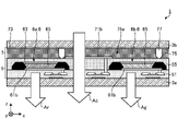
- FIG. 1 is a cross-sectional view schematically showing an example of the configuration of the transparent display device according to the first embodiment.
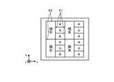
- FIG. 2 is a plan view schematically showing an example of the configuration of the transparent display device according to the first embodiment.
- FIG. 3 is a plan view schematically showing another example of the configuration of the transparent display device according to the first embodiment.
- FIG. 4 is a cross-sectional view schematically showing an example of the configuration of the transparent display device according to the first embodiment in a transmissive mode.
- FIG. 5 is a cross-sectional view schematically showing an example of the configuration in the dimming mode of the transparent display device according to the first embodiment.
- FIG. 6 is a cross-sectional view schematically showing an example of the configuration in the transmission mode of the transparent display device according to the second embodiment.
- FIG. 7 is a cross-sectional view schematically showing an example of the configuration in the dimming mode of the transparent display device according to the second embodiment.
- FIG. 8 is a cross-sectional view schematically showing an example of the configuration in the transmission mode of the transparent display device according to the third embodiment.
- FIG. 9 is a cross-sectional view schematically showing an example of the configuration in the dimming mode of the transparent display device according to the third embodiment.
- FIG. 10 is a cross-sectional view schematically showing an example of the configuration in the transmission mode of the transparent display device according to the fourth embodiment.
- FIG. 11 is a cross-sectional view schematically showing an example of the configuration in the dimming mode of the transparent display device according to the fourth embodiment.
- FIG. 12 is a cross-sectional view schematically showing an example of the configuration in the transmission mode of the transparent display device according to the fifth embodiment.
- FIG. 13 is a cross-sectional view schematically showing an example of the configuration in the dimming mode of the transparent display device according to the fifth embodiment.
- FIG. 14 is a cross-sectional view schematically showing an example of the configuration in the transmission mode of the transparent display device according to the sixth embodiment.
- FIG. 15 is a cross-sectional view schematically showing an example of the configuration in the dimming mode of the transparent display device according to the sixth embodiment.
- FIG. 16 is a cross-sectional view schematically showing an example of the configuration in the transmission mode of the transparent display device according to the seventh embodiment.
- FIG. 17 is a cross-sectional view schematically showing an example of the configuration in the dimming mode of the transparent display device according to the seventh embodiment.
- FIG. 18 is a cross-sectional view schematically showing an example of the configuration in the transmission mode of the transparent display device according to the eighth embodiment.
- FIG. 19 is a cross-sectional view schematically showing an example of the configuration in the dimming mode of the transparent display device according to the eighth embodiment.
- FIG. 20 is a cross-sectional view schematically showing an example of the configuration in the transmissive mode of the transparent display device according to the ninth embodiment.
- FIG. 21 is a cross-sectional view schematically showing an example of the configuration in the dimming mode of the transparent display device according to the ninth embodiment.
- 22 is a cross-sectional view schematically showing an example of the circuit configuration of the transparent display device according to the embodiment;
- FIG. 23 is a signal waveform diagram schematically showing an example of dimming control of the transparent display device according to the embodiment.
- a transparent display device used as a video reproducing device, a navigation device, or the like mounted on an automobile is exemplified.
- the configuration of the transparent display device according to each embodiment described below is an example, and is not limited to the following description.
- “transparent” includes the concept of “having transparency or translucency”. In other words, being “transparent” includes not only the fact that transmitted light is not absorbed, but also the fact that the degree of absorption of transmitted light is small.
- “opaque” includes the concept of "opaque or low translucency”. In other words, the term “opaque” includes not only the fact that light is not transmitted, that is, the fact that light is blocked, but also that the degree of absorption of transmitted light is large.
- “transmittance” refers to the ratio of the brightness (light amount) of visible light passing through the panel to the brightness (light amount) of visible light incident on the panel. In other words, “transmittance” is the transmittance for visible light.
- the front and back surfaces of the transparent display device are assumed to be planes parallel to the xy plane. It is also assumed that the direction from the rear surface to the rear surface of the transparent display device is the z+ direction. That is, in the following description, the surface side means the z+ side. Similarly, the back side refers to the z-side.
- FIG. 1 is a cross-sectional view schematically showing an example of the configuration of a transparent display device 1 according to the first embodiment. It is assumed that the transparent display device 1 according to this embodiment is an organic EL display (OLED). Further, it is assumed that the transparent display device 1 according to this embodiment is a bottom emission type transparent display. That is, the display surface of the transparent display device 1 according to this embodiment is provided on the back side.
- OLED organic EL display
- the transparent display device 1 has a pair of glass substrates 3a and 3b. A pair of the glass substrate 3a and the glass substrate 3b are spaced apart substantially in parallel. A TFT (Thin Film Transistor) substrate 5 and a light control layer 7 are provided between a pair of glass substrates 3a and 3b.
- TFT Thin Film Transistor
- the glass substrate 3 a is provided on the back side of the transparent display device 1 .
- the glass substrate 3 b is provided on the front side of the transparent display device 1 .
- Each of the glass substrates 3a and 3b is transparent to visible light.
- Each of the glass substrate 3a and the glass substrate 3b has, for example, a rectangular plate-like shape.
- the glass substrate 3a is an example of the first substrate.
- the glass substrate 3b is an example of a second substrate.
- the TFT substrate 5 is provided on the front side of the glass substrate 3a on the back side.
- a-Si, LTPS, IGZO, or the like can be appropriately used.
- the TFT substrate 5 is formed of, for example, a plate-like member, but may be formed of a film-like member.
- a plurality of TFTs 102 (see FIG. 22) are arranged in a matrix on the TFT substrate 5 .
- Each of the plurality of TFTs 102 has a gate electrode 53a and source-drain electrodes 53b.
- the source/drain electrodes 53b are provided on the surface side at positions corresponding to the gate electrodes 53a.
- each of the plurality of TFTs 102 is covered with an insulating member 51 .
- the insulating member 51 may be made of a material that is transparent to visible light and has electrical insulation. Silicon nitride (SiN), for example, can be used as the insulating member 51 .
- a plurality of light-emitting portions 6 are provided on the TFT substrate 5 .
- Each of the multiple light-emitting units 6 corresponds to each of the multiple light-emitting pixels 100 (see FIG. 22) of the transparent display device 1 .
- Each of the plurality of light emitting units 6 is configured to emit light independently of each other.
- Each of the plurality of light emitting portions 6 is electrically connected to the source-drain electrode 53b of the TFT 102 via a transparent electrode 61a extending inside the insulating member 51 in the z-direction.
- the transparent electrode 61a is an electrode transparent to visible light.
- Each of the plurality of light emitting units 6 is separated from the TFT 102 by an insulating member 51, for example.
- Each of the plurality of light emitting units 6 has a transparent electrode 61b, a reflective electrode 63 and a light emitting layer 65. As shown in FIG. The transparent electrode 61b and the reflective electrode 63 are arranged substantially parallel to each other. A light-emitting layer 65 is provided between the transparent electrode 61 b and the reflective electrode 63 .
- the TFT substrate 5 is an example of the first internal layer.
- the transparent electrode 61b is provided on the rear surface side of each of the plurality of light emitting units 6.
- the transparent electrode 61b is electrically connected to the transparent electrode 61a.
- the transparent electrode 61b is transparent to visible light.
- the transparent electrode 61b has, for example, a rectangular plate-like shape.
- the reflective electrode 63 is provided on the surface side of each of the plurality of light emitting parts 6 .
- the reflective electrode 63 is provided at a position facing the transparent electrode 61b.
- the reflective electrode 63 has, for example, the same shape as the transparent electrode 61b.
- the reflective electrode 63 is opaque to visible light.
- the reflective electrode 63 is made of metal, for example.
- the reflective electrode 63 is formed of glass, resin, or the like having a metal layer on its surface.
- the light emitting layer 65 is a light emitting diode (LED) made of an organic compound.
- the light-emitting layer 65 emits light when a voltage exceeding the threshold voltage is applied between the transparent electrode 61b and the reflective electrode 63.
- FIG. 1 A light emitting diode (LED) made of an organic compound.
- the light-emitting layer 65 emits light when a voltage exceeding the threshold voltage is applied between the transparent electrode 61b and the reflective electrode 63.
- the insulating member 55 may be made of a material that is transparent to visible light and has electrical insulating properties. Silicon nitride (SiN), for example, can be used as the insulating member 55 .
- a dimming layer 7 is provided on the surface side of the TFT substrate 5 .
- the light modulating layer 7 has a transparent electrode 71 a , a transparent electrode 71 b , a transparent electrode 73 , a light modulating member 75 and a spacer 77 .
- the light modulating layer 7 is an example of the second internal layer.
- the transparent electrode 71 b is provided on the surface side of the insulating member 55 .
- the transparent electrode 71b is electrically connected to the source-drain electrode 53b of the TFT 102 via the transparent electrode 71a extending in the z-direction inside the insulating members 51 and 55. As shown in FIG.
- the transparent electrode 71b is transparent to visible light.
- the transparent electrode 71b has, for example, a rectangular plate-like shape.
- the transparent electrode 73 is provided on the surface side of the insulating member 55 via the spacer 77 .
- the transparent electrode 73 is spaced apart from the transparent electrode 71b by the length of the spacer 77 in the z direction and provided substantially parallel to the transparent electrode 71b.
- a glass substrate 3 a is provided on the surface side of the transparent electrode 73 .
- the transparent electrode 73 is transparent to visible light.
- the transparent electrode 73 has, for example, a rectangular plate-like shape.
- a light control member 75 is filled between the transparent electrode 71b and the transparent electrode 73 . That is, the spacer 77 is a member for forming a gap between the transparent electrode 71b and the transparent electrode 73 to be filled with the light control member 75. As shown in FIG.
- the light control member 75 is transparent to visible light when no voltage is applied between the transparent electrode 71b and the transparent electrode 73. As shown in FIG. Hereinafter, a state in which the light control member 75 is transparent to visible light is referred to as a transmission mode.
- the dimming member 75 is opaque to visible light between the transparent electrodes 71b and 73 when a voltage exceeding the threshold voltage is applied between the transparent electrodes 71b and 73 .
- a state in which the light control member 75 is opaque to visible light is referred to as a light control mode.
- Guest-host liquid crystal, PNLC (Polymer Dispersed Liquid Crystal), SPD (Suspended Particles), electrochromic material, or the like can be appropriately used as the light control member 75 .
- the light control member 75 may be appropriately selected according to, for example, characteristics such as operating voltage and response speed. For example, the light control member 75 transitions between the transmission mode and the light control mode according to the voltage applied between the transparent electrode 71b and the transparent electrode 73 by the TFT substrate 5.
- the light modulating member 75 changes its transmittance with respect to visible light according to the voltage applied between the transparent electrode 71b and the transparent electrode 73 by the TFT substrate 5 . Therefore, it is preferable that the light control member 75 has a low operating voltage required for mode transition to the extent that it can be driven by the TFT substrate 5 .
- a structure in which the light control member 75 is sandwiched between the transparent electrodes 71b and the transparent electrodes 73 is sometimes referred to as a light control pixel.
- FIG. 2 is a plan view schematically showing an example of the configuration of the transparent display device 1 according to the first embodiment.
- FIG. 3 is a plan view schematically showing another example of the configuration of the transparent display device 1 according to the first embodiment.
- the transparent display device 1 as shown in FIGS. 2 and 3, has a light emitting area R1 and a dimming area R2. As shown in FIGS. 2 and 3, the light emitting region R1 and the dimming region R2 are regions different from each other in plan view.
- the light emitting region R1 is a region of the TFT substrate 5 where each pixel is arranged. That is, the light emitting region R1 is a region in which the light emitting section 6 is provided.
- FIG. 2 illustrates a case where R pixels, G pixels, and B pixels are provided in the light emitting region R1.
- R pixels, G pixels, B pixels, and W pixels may be provided in the light emitting region R1.
- the light control region R2 is a region corresponding to a portion of the light control layer 7 located between the transparent electrode 71b and the transparent electrode 73. That is, the light control region R2 is a region corresponding to a portion of the light control layer 7 where the transparent electrode 71b is provided.
- the light control region R2 is also a region in which light control pixels are provided.
- the dimming region R2 is provided at least in a transparent region provided between pixels of the TFT substrate 5 in plan view. More specifically, in the example shown in FIG. 1, the light emitting section 6 and the transparent electrode 71b are regions different from each other in a plan view.
- the light emitting unit 6a corresponds to the R pixel and emits red light. It is also assumed that the light emitting unit 6b emits green light.
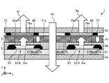
- FIG. 4 is a cross-sectional view schematically showing an example of the configuration of the transparent display device 1 according to the first embodiment in the transmission mode.
- the light-emitting portion 6a emits red light from the light-emitting layer 65 to the back side as indicated by an arrow Ar in FIG.
- the light-emitting portion 6b emits green light from the light-emitting layer 65 to the back side, as indicated by an arrow Ag in FIG.
- the light control member 75 is transparent to visible light. Therefore, external light Ac entering the transparent display device 1 from the front side is transmitted through the transmission mode light control member 75a and emitted from the back side.
- the external light incident on the transparent display device 1 from the back side passes through the transmissive mode light control member 75a and is emitted from the front side.
- FIG. 5 is a cross-sectional view schematically showing an example of the configuration in the dimming mode of the transparent display device 1 according to the first embodiment.
- the light-emitting portions 6a and 6b emit visible light to the back side in the same manner as in the transmissive mode.
- the light control member 75 is opaque to visible light between the transparent electrode 71b and the transparent electrode 73. . Therefore, external light Ac entering the transparent display device 1 from the surface side is blocked by the dimming member 75b in the dimming mode. It should be noted that external light entering the transparent display device 1 from the back side is also blocked by the dimming member 75b in the dimming mode.
- the transparent display device 1 can display an image superimposed on the background scenery, for example.
- a technique in which a dimming device for changing the transmittance of visible light is attached to the back side of the self-luminous transparent display.
- a dimming device for changing the transmittance of visible light is attached to the back side of the self-luminous transparent display.
- the transmittance of visible light is changed in the entire display area, the area other than the displayed image is also dimmed.
- the lattice pattern of the transparent display is a pattern based on the structure between the pixels of the transparent display or between the light-emitting region and the transparent region.
- the lattice pattern of the light control device is a pattern based on the structure between the pixels of the light control device.
- the transmittance varies greatly depending on the viewing angle due to the distance of several millimeters between the transparent display and the light control device.
- the transparent electrode 71b of the light control layer 7 overlaps the area between the pixels of the TFT substrate 5, that is, the area through which external light can pass in plan view. It is provided in the area where A transparent electrode 73 is provided on the side of the glass substrate 3b facing the transparent electrode 71b. A liquid crystal material is sealed between the transparent electrodes 71b and 73 to change the transmittance. According to this configuration, by applying a voltage exceeding the threshold voltage between the transparent electrode 71b and the transparent electrode 73, in the region overlapping the region through which external light can be transmitted in plan view, the liquid crystal transmits visible light. You can change the rate.
- the transparent display device 1 of the first embodiment further improvements can be achieved.
- visibility can be improved.
- the light control layer 7 is formed on the TFT substrate 5 .
- the TFT substrate 5 and the light control layer 7 are integrally formed. For this reason, compared to the case where the transparent display and the light control device formed independently are bonded together, the position of the transparent region between the light emitting regions R1 of the TFT substrate 5 and the light control region R2 of the light control layer 7 is reduced. Displacement can be suppressed.
- the TFT substrate 5 and the light control layer 7 are integrally formed, so it is necessary to provide a glass substrate between the TFT substrate 5 and the light control layer 7. do not have. Therefore, according to the technology according to the present embodiment, compared to the case of bonding a transparent display and a light control device formed independently, the number of glass substrates can be reduced from four to two, resulting in a thinner display. And weight reduction can be realized.
- FIG. 6 is a cross-sectional view schematically showing an example of the configuration of the transparent display device 1 according to the second embodiment in the transmissive mode.
- FIG. 7 is a cross-sectional view schematically showing an example of the configuration in the dimming mode of the transparent display device 1 according to the second embodiment.
- the light modulating layer 7 of the transparent display device 1 may not have the spacers 77 .
- the gap filled with the light control member 75 in the light control layer 7 is formed by an insulating member 55 covering the light emitting portion 6 of the TFT substrate 5, as shown in FIGS.
- the transparent electrode 71 b is provided on the surface side of the insulating member 51 .
- the transparent electrode 71b is electrically connected to the source-drain electrode 53b of the TFT 102 via the transparent electrode 71a extending inside the insulating member 51 in the z-direction.
- the transparent electrode 73 is provided on the surface side of the insulating member 51 with the insulating member 55 interposed therebetween. In other words, the transparent electrode 73 is separated from the transparent electrode 71b by the length in the z direction of the insulating member 55 covering the light emitting section 6, and is provided substantially parallel to the transparent electrode 71b.
- the visibility can be improved as in the transparent display device 1 according to the first embodiment.
- the layer provided with the insulating member 55 of the TFT substrate 5 and the light control layer 7 are integrally formed, the thickness and weight of the transparent display device 1 can be reduced as compared with the transparent display device 1 according to the first embodiment. can be realized.
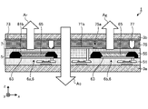
- FIG. 8 is a cross-sectional view schematically showing an example of the configuration in the transmission mode of the transparent display device 1 according to the third embodiment.
- FIG. 9 is a cross-sectional view schematically showing an example of the configuration in the dimming mode of the transparent display device 1 according to the third embodiment.
- the transparent display device 1 according to this embodiment may be a top emission type transparent display. That is, the display surface of the transparent display device 1 according to this embodiment is provided on the front side.
- the transparent electrode 61b is provided on the surface side of each of the plurality of light emitting portions 6, as shown in FIGS.
- the reflective electrode 63 is provided at a position facing the transparent electrode 61b on the rear surface side of each of the plurality of light-emitting portions 6 .
- the reflective electrode 63 is electrically connected to the transparent electrode 61a.
- the light-emitting portion 6a emits red light from the light-emitting layer 65 to the surface side, as indicated by arrows Ar in FIGS.
- the light-emitting portion 6b emits green light from the light-emitting layer 65 to the surface side, as indicated by an arrow Ag in FIGS.
- external light Ac entering the transparent display device 1 from the front side is transmitted through the transmission mode light control member 75a and emitted from the back side.
- external light Ac entering the transparent display device 1 from the front side is blocked by the dimming member 75b in the dimming mode.
- the transparent display device 1 according to this embodiment is configured as a top emission type transparent display.
- the dimming layer 7 is provided on the display surface side. Even with this configuration, the visibility can be improved as in the transparent display device 1 according to the first embodiment.
- the layer provided with the insulating member 55 of the TFT substrate 5 and the light control layer 7 are integrated in the same manner as in the transparent display device 1 according to the second embodiment. may be formed.
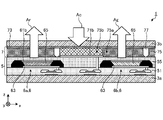
- FIG. 10 is a cross-sectional view schematically showing an example of the configuration in the transmission mode of the transparent display device 1 according to the fourth embodiment.
- FIG. 11 is a cross-sectional view schematically showing an example of the configuration in the dimming mode of the transparent display device 1 according to the fourth embodiment.
- Each of the plurality of light emitting units 6 has the same light emitting layer 65, for example. As an example, it is assumed that each of the plurality of light emitting portions 6c emits white light as indicated by arrows Aw in FIGS. 10 and 11. FIG.
- the transparent display device 1 further has a plurality of color filters 79 .
- Each of the plurality of color filters 79 is provided between the transparent electrode 73 and the glass substrate 3b.
- Each of the multiple color filters 79 is provided at a position overlapping the multiple light emitting units 6 in plan view.
- Each of the plurality of color filters 79 has predetermined wavelength selectivity.
- the color filter 79a is, for example, a color filter that transmits red light.
- the color filter 79b is, for example, a color filter that transmits green light.
- the white light emitted from the plurality of light emitting portions 6c is incident on the corresponding color filters 79 respectively.
- Each of the plurality of color filters 79 emits visible light including wavelengths corresponding to wavelength selectivity to the rear surface side. Even with this configuration, the visibility can be improved as in the transparent display device 1 according to the first embodiment.
- each of the plurality of light-emitting portions 6c may be an OLED that emits visible light in any wavelength region, not limited to white light.
- the wavelength selectivity of the color filter 79 may be determined according to the wavelength range of the visible light emitted from the light emitting section 6c.
- the transparent display device 1 according to the present embodiment may be configured as a top emission type transparent display in the same manner as the transparent display device 1 according to the first embodiment or the second embodiment.
- each of the plurality of color filters 79 may be provided on the back surface side of the corresponding light emitting portion 6c.
- the layer provided with the insulating member 55 of the TFT substrate 5 and the light control layer 7 are integrated in the same manner as in the transparent display device 1 according to the second embodiment. may be formed.
- the light control member 75 of the light control layer 7 may be filled between the plurality of color filters 79 .
- FIG. 12 is a cross-sectional view schematically showing an example of the configuration of the transparent display device 1 according to the fifth embodiment in transmission mode.
- FIG. 13 is a cross-sectional view schematically showing an example of the configuration in the dimming mode of the transparent display device 1 according to the fifth embodiment.
- the transparent display device 1 may be a transparent display having display surfaces on both the front side and the back side.
- the transparent electrode 61b is provided on the rear surface side of each of the plurality of light emitting portions 6, as shown in FIGS.
- the transparent electrode 61b is electrically connected to the transparent electrode 61a.
- the transparent display device 1 according to this embodiment has a transparent electrode 61 c instead of the reflective electrode 63 .
- the transparent electrode 61c is provided at a position facing the transparent electrode 61b on the surface side of each of the plurality of light emitting portions 6. As shown in FIG.
- the transparent electrode 61c is transparent to visible light.
- the transparent electrode 61c has, for example, the same shape as the transparent electrode 61b.
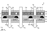
- the light-emitting portion 6a emits red light from the light-emitting layer 65 to both the front side and the back side, as indicated by arrows Ar in FIGS.
- the light-emitting portion 6b emits green light from the light-emitting layer 65 to both the front side and the back side, as indicated by arrows Ag in FIGS.
- external light Ac entering the transparent display device 1 from the front side is transmitted through the transmission mode light control member 75a and emitted from the back side.
- external light Ac entering the transparent display device 1 from the front side is blocked by the dimming member 75b in the dimming mode.
- external light entering the transparent display device 1 from the back side is also blocked by the dimming member 75b in the dimming mode.
- the transparent display device 1 according to this embodiment is configured as a transparent display having display surfaces on both the front side and the back side. Even with this configuration, the visibility can be improved as in the transparent display device 1 according to the first embodiment.
- the layer provided with the insulating member 55 of the TFT substrate 5 and the light control layer 7 are integrated in the same manner as in the transparent display device 1 according to the second embodiment. may be formed.
- the transparent display device 1 according to this embodiment may be provided with a plurality of color filters 79 in the same manner as the transparent display device 1 according to the fourth embodiment.
- the plurality of color filters 79 may be provided on the rear surface side of the corresponding light emitting portion 6c in addition to between the transparent electrode 73 and the glass substrate 3b.
- FIG. 14 is a cross-sectional view schematically showing an example of the configuration in the transmission mode of the transparent display device 1 according to the sixth embodiment.
- FIG. 15 is a cross-sectional view schematically showing an example of the configuration in the dimming mode of the transparent display device 1 according to the sixth embodiment.
- the transparent display device 1 may be a transparent display configured to block visible light from each of the plurality of light emitting units 6 in the dimming mode.
- the transparent electrode 71b is provided over the entire light control layer 7, as shown in FIGS.
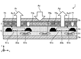
- the light-emitting portion 6a transmits the red light from the light-emitting layer 65 through the transmission-mode light control member 75a and emits it to the surface side.
- the light-emitting portion 6a also emits red light from the light-emitting layer 65 to the back side as indicated by an arrow Ar in FIG.
- the light-emitting portion 6b emits the green light from the light-emitting layer 65 to the surface side through the light control member 75a in the transmission mode, as indicated by the arrow Ag in FIG.
- the light-emitting portion 6b also emits green light from the light-emitting layer 65 to the back side as indicated by an arrow Ag in FIG.
- external light Ac entering the transparent display device 1 from the front side is transmitted through the transmission mode light control member 75a and emitted from the back side.
- the red light emitted from the light emitting unit 6a toward the front side, the green light emitted from the light emitting unit 6b toward the front side, and the external light Ac entering the transparent display device 1 from the front side or the back side are As shown in FIG. 15, each light is shielded by the dimming member 75b in the dimming mode.
- the transparent display device 1 according to this embodiment is configured as a transparent display having display surfaces on both the front side and the back side. Even with this configuration, the visibility of the display surface on the back side can be improved as in the case of the transparent display device 1 according to the first embodiment.
- the layer provided with the insulating member 55 of the TFT substrate 5 and the light control layer 7 are integrated in the same manner as in the transparent display device 1 according to the second embodiment. may be formed.
- the transparent display device 1 according to this embodiment may be provided with a plurality of color filters 79 in the same manner as the transparent display device 1 according to the fourth embodiment.
- the plurality of color filters 79 may be provided on the rear surface side of the corresponding light emitting portion 6c in addition to between the transparent electrode 73 and the glass substrate 3b.
- FIG. 16 is a cross-sectional view schematically showing an example of the configuration of the transparent display device 1 according to the seventh embodiment in the transmissive mode.
- FIG. 17 is a cross-sectional view schematically showing an example of the configuration in the dimming mode of the transparent display device 1 according to the seventh embodiment.
- the light control member 75 may have a light control function in combination with the polarizing plate 81 .
- the transparent display device 1 further includes a polarizing plate 81a and a polarizing plate 81b, as shown in FIGS.
- the polarizing plate 81a is provided on the back side of the glass substrate 3a.
- the polarizing plate 81b is provided on the surface side of the glass substrate 3b.
- the polarizing plate 81a and the polarizing plate 81b may each be formed of a plate-like member, or may be formed of a film-like member.
- the polarizing plate 81a is an example of a first polarizing layer.
- the polarizing plate 81b is an example of a second polarizing layer.
- the transparent display device 1 provided with the polarizing plate 81 it is preferable that visibility due to external light can be improved even when the user is wearing polarized sunglasses, for example.
- TN Transmission Nematic
- VA Very Alignment
- IPS In Plane Switching
- the absorption axis of polarized sunglasses is, for example, 0° (horizontal direction).
- the transparent display device 1 it is assumed that there are users on both the front side and the back side.
- polarizing plates are arranged with a 90° shift between the front and back sides.
- the absorption axis of the polarizer is placed at 90° (vertical direction)
- the light from the display cannot pass through polarized sunglasses with an absorption axis of 0°, so the user cannot see the display.
- the polarizing plates 81a and 81b are arranged so that their absorption axes are both at 0°. According to this configuration, the transmittance through polarized sunglasses having an absorption axis of 0° can be maximized compared to other combinations of absorption axes.
- the polarizing plates 81a and 81b are arranged so that their absorption axes are both at 45°.
- the absorption axis of the polarizing plate 81a and the absorption axis of the polarizing plate 81b can be shifted by 90°.
- the non-polarized external light incident on the polarizing plate 81b on the front side is polarized into linearly polarized light with an inclination of -45° by the polarizing plate 81b with an absorption axis of 45°.
- the liquid crystal molecules of the TN mode are twisted at 90° and oriented.
- the retardation of liquid crystal is ⁇ /2. Therefore, the light transmitted through the dimming member 75 has linear polarization of 45°.
- linearly polarized light with an inclination of 45° incident on the polarizing plate 81a on the back side can pass through the polarizing plate 81a with an absorption axis of ⁇ 45°.
- the liquid crystal molecules of the TN system are vertically aligned.
- the phase difference of liquid crystal is zero. Therefore, the light transmitted through the light adjusting member 75 is linearly polarized with an inclination of ⁇ 45°, and therefore cannot be transmitted through the polarizing plate 81a with the absorption axis of ⁇ 45° as shown in FIG.
- the transparent display device 1 using TN liquid crystal as the light control member 75 can block external light by applying a voltage between the transparent electrode 71b and the transparent electrode 73. Thereby, the transparent display device 1 can improve the visibility of the display.
- the light control member is VA liquid crystal
- VA liquid crystal if the absorption axis of the polarizing plate 81 is arranged at the same angle on both the front and back sides to obtain normally white, the black does not sink, that is, the contrast does not appear. Black is preferred.
- the liquid crystal molecules of the VA mode are vertically aligned.
- the phase difference of liquid crystal is zero. Therefore, the light transmitted through the light control member 75 is linearly polarized with an inclination of ⁇ 45°, and therefore cannot transmit through the polarizing plate 81a on the back side of the absorption axis of ⁇ 45° as shown in FIG.
- the liquid crystal molecules of the VA mode are oriented in the 0° and/or 90° directions.
- the retardation of liquid crystal is ⁇ /2. Therefore, since the light transmitted through the light control member 75 has right elliptically polarized light and left elliptical polarized light with an inclination of 45°, as shown in FIG. can be transmitted through the polarizing plate 81a on the side.
- the transparent display device 1 using VA liquid crystal as the light control member 75 can block external light by not applying a voltage between the transparent electrode 71b and the transparent electrode 73. Thereby, the transparent display device 1 can improve the visibility of the display.
- the light control member is an IPS liquid crystal
- the IPS mode liquid crystal molecules are oriented at 45°.
- the retardation of liquid crystal is ⁇ /2. Therefore, the light transmitted through the light control member 75 is linearly polarized with an inclination of ⁇ 45°, and therefore cannot transmit through the polarizing plate 81a on the back side of the absorption axis of ⁇ 45° as shown in FIG.
- the IPS mode liquid crystal molecules are oriented in the 0° and/or 90° direction.
- the retardation of liquid crystal is ⁇ /2. Therefore, since the light transmitted through the light control member 75 has right elliptically polarized light and left elliptical polarized light with an inclination of 45°, as shown in FIG. can be transmitted through the polarizing plate 81a on the side.
- the transparent display device 1 using IPS liquid crystal as the light control member 75 can block external light by not applying a voltage between the transparent electrodes 71b and 73. Thereby, the transparent display device 1 can improve the visibility of the display.
- the respective absorption axes of the polarizing plates 81 a and 81 b are defined according to the orientation of the liquid crystal used as the light control member 75 . Therefore, according to the technique according to the present embodiment, by combining the light control member 75 and the polarizing plate 81, it is possible to achieve light control for each pixel in the same manner as in the above-described embodiments.
- the layer provided with the insulating member 55 of the TFT substrate 5 and the light control layer 7 are integrated in the same manner as in the transparent display device 1 according to the second embodiment. may be formed.
- the transparent display device 1 according to the present embodiment may be configured as a top emission type transparent display in the same manner as the transparent display device 1 according to the third embodiment.
- the transparent display device 1 according to this embodiment may be provided with a plurality of color filters 79 in the same manner as the transparent display device 1 according to the fourth embodiment.
- the transparent display device 1 according to this embodiment has display surfaces on both the front side and the back side in the same manner as the transparent display device 1 according to the fifth embodiment or the sixth embodiment. It may be configured as a display.
- the transparent display device 1 according to the present embodiment is configured to block visible light from each of the plurality of light emitting units 6 in the dimming mode in the same manner as the transparent display device 1 according to the sixth embodiment. It may also be a transparent display with a
- FIG. 18 is a cross-sectional view schematically showing an example of the configuration of the transparent display device 1 according to the eighth embodiment in transmission mode.
- FIG. 19 is a cross-sectional view schematically showing an example of the configuration in the dimming mode of the transparent display device 1 according to the eighth embodiment.
- the light modulating member 75 may have a light modulating function and a low reflection function in combination with the polarizing plate 81 and the ⁇ /4 retardation plate 83 .
- the transparent display device 1 further includes a ⁇ /4 retardation plate 83a and a ⁇ /4 retardation plate 83b.
- the ⁇ /4 retardation plate 83a is provided between the glass substrate 3a and the polarizing plate 81a.
- the ⁇ /4 retardation plate 83b is provided between the glass substrate 3b and the polarizing plate 81b.
- Each of the ⁇ /4 retardation plate 83a and the ⁇ /4 retardation plate 83b may be formed of a plate-like member or a film-like member.
- the ⁇ /4 retardation plate 83a is an example of the first retardation layer.
- the ⁇ /4 retardation plate 83b is an example of a second retardation layer.
- the transparent display device 1 provided with the polarizing plate 81 it is preferable to be able to suppress deterioration in visibility due to external light even when the user is wearing polarized sunglasses, for example. Further, it is more preferable to be able to suppress deterioration in visibility due to reflected light of external light from the light emitting portion 6 such as an OLED provided on the TFT substrate 5 and wiring such as electrodes.
- the light emitting portion 6 such as an OLED provided on the TFT substrate 5 and wiring such as electrodes.
- VA Very Alignment
- the light incident on the light control member 75 that is, the light transmitted through the ⁇ /4 retardation plate 83, becomes circularly polarized light. It is preferable to define
- the absorption axes of the polarizing plates 81a and 81b on the front and back sides are both 0°, and the ⁇ /4 retardation plates 83a and 83b on the front and back sides are retarded.
- both phase axes are 45° will be described as an example.
- the unpolarized external light incident on the polarizing plate 81b on the front side is polarized into linearly polarized light with an inclination of 90° by the polarizing plate 81b with an absorption axis of 0°, and then passes through a ⁇ /4 retardation plate with a slow axis of 45°.
- 83b polarizes it to left circular polarization.
- the liquid crystal molecules of the TN mode are twisted at 90° and oriented.
- the retardation of liquid crystal is ⁇ /2.
- the linearly polarized component with an inclination of 90° is transmitted through the ⁇ /4 retardation plate 83a with a slow axis of 45° on the back side.
- linearly polarized light with an inclination of 90° that is incident on the polarizing plate 81a on the back side can pass through the polarizing plate 81a with an absorption axis of 0°, as shown in FIG.
- the light transmitted through the light control member 75 has right circularly polarized light. Therefore, the light reflected by the TFT substrate 5 on the back side of the light control member 75 has left-handed circularly polarized light. Therefore, since the light transmitted through the light control member 75 has right-handed circularly polarized light, a linearly polarized component with an inclination of 0° is transmitted through the ⁇ /4 retardation plate 83b with a slow axis of 45° on the surface side. As a result, the linearly polarized light with an inclination of 0° incident on the ⁇ /4 retardation plate 83b with the slow axis of 45° on the front side cannot pass through the polarizing plate 81b with the absorption axis of 0°.
- the transparent display device 1 using TN liquid crystal as the light control member 75 can block external light by applying a voltage between the transparent electrode 71b and the transparent electrode 73. Thereby, the transparent display device 1 can improve the visibility of the display. In addition, it is possible to suppress the light reflected by the TFT substrate 5 of the external light from the front surface side from being emitted to the front surface side.
- the slow axis of either one of the ⁇ /4 retardation plate 83a and the ⁇ /4 retardation plate 83b on the front side and the back side can be set to ⁇ 45°.
- the transparent display device 1 using TN liquid crystal as the light control member 75 can block external light by not applying a voltage between the transparent electrode 71b and the transparent electrode 73. FIG. Thereby, the transparent display device 1 can improve the visibility of the display. Further, similarly to the case described above, it is possible to suppress the light reflected by the TFT substrate 5 of the external light from the front surface side from being emitted to the front surface side.
- the light transmitted through the light control member 75 has left circularly polarized light. Therefore, the light reflected by the TFT substrate 5 on the back side of the light control member 75 has right circularly polarized light. Therefore, since the light transmitted through the light control member 75 has right-handed circularly polarized light, a linearly polarized component with an inclination of 0° is transmitted through the ⁇ /4 retardation plate 83b with a slow axis of 45° on the surface side. As a result, the linearly polarized light with an inclination of 0° incident on the ⁇ /4 retardation plate 83b with the slow axis of 45° on the front side cannot pass through the polarizing plate 81b with the absorption axis of 0°.
- the liquid crystal molecules of the VA mode are oriented at 45° and/or -45°.
- the retardation of liquid crystal is ⁇ /2. Therefore, since the light transmitted through the light control member 75 has right circularly polarized light and left circularly polarized light, the right elliptical polarized light and left elliptical polarized light pass through the ⁇ /4 retardation plate 83a having a slow axis of 45° on the back side. To Penetrate. As a result, of the right-handed elliptically polarized light and left-handed elliptically polarized light incident on the polarizing plate 81a on the back side, as shown in FIG. can do.
- the transparent display device 1 using VA liquid crystal as the light control member 75 can block external light by not applying a voltage between the transparent electrode 71b and the transparent electrode 73. Thereby, the transparent display device 1 can improve the visibility of the display. In addition, it is possible to suppress the light reflected by the TFT substrate 5 of the external light from the front surface side from being emitted to the front surface side.
- the slow axis of either one of the ⁇ /4 retardation plate 83a and the ⁇ /4 retardation plate 83b on the front side and the back side can be set to ⁇ 45°.
- the transparent display device 1 using VA liquid crystal as the light control member 75 can block external light by applying a voltage between the transparent electrode 71b and the transparent electrode 73. FIG. Thereby, the transparent display device 1 can improve the visibility of the display. Further, similarly to the case described above, it is possible to suppress the light reflected by the TFT substrate 5 of the external light from the front surface side from being emitted to the front surface side.
- the transparent display device 1 according to the seventh embodiment, by combining the light control member 75, the polarizing plate 81 and the ⁇ /4 retardation plate 83, the pixel unit dimming can be achieved. In addition, it is possible to suppress deterioration in visibility due to reflected light of external light on the TFT substrate 5 .
- the layer provided with the insulating member 55 of the TFT substrate 5 and the light control layer 7 are integrated in the same manner as in the transparent display device 1 according to the second embodiment. may be formed.
- the transparent display device 1 according to the present embodiment may be configured as a top emission type transparent display in the same manner as the transparent display device 1 according to the third embodiment.
- the transparent display device 1 according to this embodiment may be provided with a plurality of color filters 79 in the same manner as the transparent display device 1 according to the fourth embodiment.
- the transparent display device 1 according to this embodiment has display surfaces on both the front side and the back side in the same manner as the transparent display device 1 according to the fifth embodiment or the sixth embodiment. It may be configured as a display.
- the transparent display device 1 according to the present embodiment is configured to block visible light from each of the plurality of light emitting units 6 in the dimming mode in the same manner as the transparent display device 1 according to the sixth embodiment. It may also be a transparent display with a
- FIG. 20 is a cross-sectional view schematically showing an example of the configuration in the transmission mode of the transparent display device 1 according to the ninth embodiment.
- FIG. 21 is a cross-sectional view schematically showing an example of the configuration in the dimming mode of the transparent display device 1 according to the ninth embodiment.
- the transparent display device 1 may be a transparent display configured using LEDs 85 such as mini-LEDs or micro-LEDs, not limited to OLEDs, as the light-emitting portion 6 .
- LEDs 85 such as mini-LEDs or micro-LEDs, not limited to OLEDs, as the light-emitting portion 6 .
- 20 and 21 illustrate LED 85a and LED 85b as LED 85.
- the LED 85 of the light emitting section 6 is electrically connected to the transparent electrodes 61b and 61c.
- the LED 85a of the light emitting section 6a is a red light emitting diode.
- the LED 85b of the light emitting section 6b is a green light emitting diode.
- the transparent display device 1 has the LEDs 85 such as mini LEDs or micro LEDs instead of OLEDs as the light emitting section 6 . Even with this configuration, the visibility can be improved as in the transparent display device 1 according to the first embodiment. In addition, it is possible to reduce the occurrence of burn-in as compared with OLED. Moreover, the life of the light emitting part 6 can be extended compared to OLED.
- the layer provided with the insulating member 55 of the TFT substrate 5 and the light control layer 7 are integrated in the same manner as in the transparent display device 1 according to the second embodiment. may be formed.
- the transparent display device 1 according to the present embodiment may be configured as a top emission type transparent display in the same manner as the transparent display device 1 according to the third embodiment.
- the transparent display device 1 according to this embodiment may be provided with a plurality of color filters 79 in the same manner as the transparent display device 1 according to the fourth embodiment.
- the transparent display device 1 according to this embodiment has display surfaces on both the front side and the back side in the same manner as the transparent display device 1 according to the fifth embodiment or the sixth embodiment. It may be configured as a display.
- the transparent display device 1 according to the present embodiment is configured to block visible light from each of the plurality of light emitting units 6 in the dimming mode in the same manner as the transparent display device 1 according to the sixth embodiment. It may also be a transparent display with a
- the transparent display device 1 according to the present embodiment has a configuration that realizes a light control function by combining the light control member 75 and the polarizing plate 81 in the same manner as the transparent display device 1 according to the seventh embodiment. may be
- the transparent display device 1 according to the present embodiment is similar to the transparent display device 1 according to the eighth embodiment. You may have the structure which implement
- FIG. 22 is a diagram schematically showing an example of the circuit configuration of the TFT substrate 5 of the transparent display device 1 according to the embodiment.
- the TFT substrate 5 has a plurality of light-emitting pixels 100 and a plurality of dimming pixels 110, as shown in FIG.
- a plurality of light-emitting pixels 100 and a plurality of dimming pixels 110 are arranged in a matrix on the TFT substrate 5 .
- the plurality of light-emitting pixels 100 are configured to be capable of emitting light independently.
- Each of the plurality of dimming pixels 110 independently changes its transmittance with respect to visible light.
- the plurality of dimming pixels 110 are arranged at positions different from the plurality of light emitting pixels 100 in plan view.
- Each of the plurality of light emitting pixels 100 has a light emitting element 101, a TFT 102, a TFT 105, a storage capacitor 106 and a storage capacitor 107, as shown in FIG.
- the anode of the light emitting element 101 is electrically connected to the drain of the TFT 102 via the transparent electrodes 61a and 61b.
- the cathode of the light emitting element 101 is electrically connected to the power supply wiring 104 on the Vss side through the reflective electrode 63 .
- the light-emitting element 101 emits light with luminance corresponding to the value of current flowing between the anode and the cathode.
- a TFT 102 is a driving transistor for the light emitting element 101 .
- the TFT 102 is, for example, a P-type TFT.
- the source and drain of TFT 102 are realized by source-drain electrodes 53b.
- a gate of the TFT 102 is realized by a gate electrode 53a.
- the source of the TFT 102 is electrically connected to the power supply wiring 103 on the Vdd side.
- the gate of TFT 102 is electrically connected to the drain of TFT 105 .
- the gate of the TFT 102 is electrically connected to the power supply wiring 103 on the Vdd side through the storage capacitor 106 and the storage capacitor 107 .
- the TFT 102 supplies the light emitting element 101 with a current corresponding to the voltage held in the holding capacitor 106 and the holding capacitor 107 .
- a TFT 105 is a switch transistor of the light emitting element 101 .
- the TFT 105 is, for example, a P-type TFT.
- a source of the TFT 105 is electrically connected to the video signal line 130 .
- the TFT 105 is turned on or off according to the voltage applied by the scanning line driving circuit 121 .
- the holding capacitors 106 and 107 hold the potential difference between the potential of the Vdd-side power supply wiring 103 when the TFT is turned off and the potential of the gate of the TFT 102 . That is, the holding capacitors 106 and 107 hold voltages corresponding to the signal voltages.
- Each of the plurality of dimming pixels 110 has a liquid crystal element 111, a TFT 113, a holding capacitor 114 and a holding capacitor 115, as shown in FIG.
- the liquid crystal element 111 corresponds to the light modulating member 75 of the light modulating layer 7 . Specifically, it corresponds to the light control member 75 positioned between the transparent electrode 71 b and the transparent electrode 73 among the light control members 75 . One end of the liquid crystal element 111 is electrically connected to the power supply wiring 112 on the Vcom side through the transparent electrode 73 . Another end of the liquid crystal element 111 is electrically connected to the drain of the TFT 113 .
- a TFT 113 is a switch transistor for the liquid crystal element 111 .
- the TFT 113 is, for example, a P-type TFT.
- a storage capacitor 114 is electrically connected between the gate and drain of the TFT 113 .
- the TFT 113 is turned on or off according to the voltage applied by the scanning line driving circuit 121 .
- the TFT substrate 5 includes a plurality of scanning lines 120, a scanning line driving circuit 121, a plurality of video signal lines 130, a video signal line driving circuit 131, a plurality of dimming signal lines 140, and a dimming signal line. It has a drive circuit 141 and an image signal timing control circuit 150 .
- the scanning line drive circuit 121 is electrically connected to the plurality of scanning lines 120 .
- FIG. 22 illustrates scanning line Gate_n and scanning line Gate_n+1 as the plurality of scanning lines 120 .
- the scanning line Gate_n is electrically connected to the gates of the TFTs 105 of the plurality of light-emitting pixels 100 and the gates of the TFTs 113 of the plurality of dimming pixels 110 .
- the scanning line Gate_n+1 is electrically connected to the drains of the respective TFTs 113 via the storage capacitors 115 of the plurality of dimming pixels 110 .
- the scanning line driving circuit 121 is electrically connected to the drain of the TFT 113 via the storage capacitor 115 .
- the scanning line driving circuit 121 sequentially scans the plurality of luminescent pixels 100 by outputting scanning signals to the plurality of scanning lines 120 . Specifically, the TFTs 105 are turned on or off row by row. As a result, the scanning line driving circuit 121 applies the signal voltages output from the video signal line driving circuit 131 to the plurality of video signal lines 130 to the plurality of light emitting pixels 100 in the selected row, thereby turning the light emitting pixels 100 on. Light is emitted at a brightness corresponding to video data.
- the scanning line driving circuit 121 sequentially scans the plurality of dimming pixels 110 by outputting scanning signals to the plurality of scanning lines 120 .
- the TFTs 113 are turned on or off row by row. Accordingly, the scanning line driving circuit 121 applies the signal voltage output from the dimming signal line driving circuit 141 to the plurality of dimming pixels 110 in the selected row, and the liquid crystal elements 111 of the dimming pixels 110 Transmittance is changed according to dimming data.
- the video signal line drive circuit 131 is electrically connected to the plurality of video signal lines 130 .
- FIG. 22 illustrates Sig_nR, Sig_nG, Sig_nB, Sig_n+1R, Sig_n+1G and Sig_n+1B as the plurality of video signal lines 130 .
- the video signal line Sig_nR is electrically connected to the source of the TFT 105 of the light emitting pixel 100 of OLED-R.
- the video signal line Sig_nG is electrically connected to the source of the TFT 105 of the OLED-G pixel 100 .
- the video signal line Sig_nB is electrically connected to the source of the TFT 105 of the light emitting pixel 100 of OLED-B.
- OLED-R is an OLED that emits red light.
- OLED-G is an OLED that emits green light.
- OLED-B is an OLED that emits blue light.
- the video signal line drive circuit 131 applies signal voltages corresponding to video data to each of the plurality of light emitting pixels 100 via the plurality of video signal lines 130 .
- the dimming signal line drive circuit 141 is electrically connected to the multiple dimming signal lines 140 .
- FIG. 22 illustrates a dimming signal line Sig_nLC and a dimming signal line Sig_n+1LC as the plurality of dimming signal lines 140 .
- the dimming signal line Sig_nLC and the dimming signal line Sig_n+1LC are electrically connected to the source of the TFT 113 of the corresponding dimming pixel 110 .
- the dimming signal line drive circuit 141 applies a signal voltage corresponding to dimming data to each of the dimming pixels 110 via the dimming signal lines 140 .
- the image signal timing control circuit 150 is electrically connected to each of the scanning line driving circuit 121, the video signal line driving circuit 131, and the dimming signal line driving circuit 141.
- the image signal timing control circuit 150 controls operation timings of the scanning line driving circuit 121, the video signal line driving circuit 131, and the dimming signal line driving circuit 141 based on the inputted image signal.
- the image signal timing control circuit 150 is an example of a control circuit.
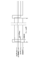
- FIG. 23 is a signal waveform diagram schematically showing an example of dimming control of the transparent display device 1 according to the embodiment.
- the image signal timing control circuit 150 controls the scanning line driving circuit 121 so as to raise the scanning line signal Vg at a timing corresponding to the input image signal.
- the scanning line driving circuit 121 generates, for example, a rectangular pulse signal at a timing according to the control of the image signal timing control circuit 150, and sequentially scans the plurality of light-emitting pixels 100 and sequentially scans the plurality of dimming pixels 110. . Therefore, the pulse width of the pulse signal corresponds to one scanning period.
- the image signal timing control circuit 150 supplies the signal voltage corresponding to the video data to the video signal line driving circuit 131, and transmits the signal voltage corresponding to the dimming data to the video signal line. It is supplied to the drive circuit 131 .
- the image signal timing control circuit 150 controls the dimming signal applied to each of the plurality of dimming pixels 110 from the dimming signal line driving circuit 141 based on the input image signal. Control the amplitude of Vsig on a frame-by-frame basis.
- the image signal timing control circuit 150 controls the amplitude of the dimming signal Vsig applied to each of the plurality of dimming pixels 110 for each frame based on the input image signal. In other words, the image signal timing control circuit 150 controls the transmittance of the liquid crystal element 111 of the dimming pixel 110 based on the input image signal.
- the image signal timing control circuit 150 controls the timing at which the scanning line signal Vg rises based on the input image signal, so that the light emission of each of the plurality of light emitting pixels 100 and the light emission of the plurality of dimming pixels 110 are controlled. Each dimming can be controlled. In other words, the image signal timing control circuit 150 can control light emission and dimming of each pixel in the transparent display device 1 with one gate pulse signal. According to this configuration, it is possible to easily realize pixel-by-pixel light control according to image data to be displayed.
- processors such as ASIC (Application Specific Integrated Circuit) and FPGA (Field Programmable Gate Array) can be used as appropriate.
- the image signal timing control circuit 150 has a processor such as a CPU (Central Processing Unit) and a memory such as a RAM (Random Access Memory). , may implement the control described above.
- the control program may be provided in advance, for example, in a ROM (Read Only Memory) or the like.
- the control program is recorded in a computer-readable recording medium such as a CD-ROM, a flexible disk (FD), a CD-R, a DVD (Digital Versatile Disk), etc. as a file in an installable format or an executable format.
- the control program may be stored on a computer connected to a network such as the Internet, and provided by being downloaded via the network.
- the control program may be configured to be provided or distributed via a network such as the Internet.
- a first substrate capable of transmitting visible light
- a first internal layer in which a plurality of light-emitting pixels, which are provided on the first main surface of the first substrate and configured to emit light independently, and regions capable of transmitting visible light are arranged
- a plurality of tone signals each independently changing transmittance with respect to visible light are provided on the side of the first inner layer opposite to the first substrate and at positions different from the plurality of light-emitting pixels in plan view.
- a second inner layer in which light pixels are arranged;
- a transparent display device comprising: a second substrate provided on the opposite side of the second inner layer from the first inner layer and capable of transmitting visible light.
- the first internal layer has a circuit configuration electrically connected to each of the plurality of light-emitting pixels;
- the second inner layer comprises: a first electrode electrically connected to the circuit configuration, provided at a position different from the plurality of light-emitting pixels in a plan view, and capable of transmitting visible light; a second electrode capable of transmitting visible light, provided on a side of the second substrate facing the first electrode and spaced apart from the first electrode; Dimming that is provided between the first electrode and the second electrode and has a transmittance for visible light that changes according to the voltage applied between the first electrode and the second electrode having a member and The transparent display device according to (1) above.
- each of the plurality of dimming pixels is provided between the plurality of light-emitting pixels in the first inner layer.
- a first polarizing layer provided on the opposite side of the first substrate from the first inner layer for polarizing visible light
- a second polarizing layer provided on the opposite side of the second substrate from the second internal layer for polarizing visible light
- each of the plurality of dimming pixels has a liquid crystal element
- the absorption axis of the first polarizing layer and the absorption axis of the second polarizing layer are defined according to the orientation of the liquid crystal element
- any of the above (1) to (4) further comprising a control circuit that controls on/off timing of switches provided in each of the plurality of light-emitting pixels and the plurality of dimming pixels, based on an image signal.
Landscapes
- Physics & Mathematics (AREA)
- General Physics & Mathematics (AREA)
- Nonlinear Science (AREA)
- Engineering & Computer Science (AREA)
- Theoretical Computer Science (AREA)
- Chemical & Material Sciences (AREA)
- Crystallography & Structural Chemistry (AREA)
- Optics & Photonics (AREA)
- Electroluminescent Light Sources (AREA)
- Devices For Indicating Variable Information By Combining Individual Elements (AREA)
Priority Applications (2)
| Application Number | Priority Date | Filing Date | Title |
|---|---|---|---|
| JP2023505190A JP7734468B2 (ja) | 2021-03-11 | 2022-01-26 | 透明ディスプレイ装置 |
| US18/238,306 US12588389B2 (en) | 2021-03-11 | 2023-08-25 | Transparent display device |
Applications Claiming Priority (2)
| Application Number | Priority Date | Filing Date | Title |
|---|---|---|---|
| JP2021-039661 | 2021-03-11 | ||
| JP2021039661 | 2021-03-11 |
Related Child Applications (1)
| Application Number | Title | Priority Date | Filing Date |
|---|---|---|---|
| US18/238,306 Continuation US12588389B2 (en) | 2021-03-11 | 2023-08-25 | Transparent display device |
Publications (1)
| Publication Number | Publication Date |
|---|---|
| WO2022190688A1 true WO2022190688A1 (ja) | 2022-09-15 |
Family
ID=83226729
Family Applications (1)
| Application Number | Title | Priority Date | Filing Date |
|---|---|---|---|
| PCT/JP2022/002954 Ceased WO2022190688A1 (ja) | 2021-03-11 | 2022-01-26 | 透明ディスプレイ装置 |
Country Status (3)
| Country | Link |
|---|---|
| US (1) | US12588389B2 (https=) |
| JP (1) | JP7734468B2 (https=) |
| WO (1) | WO2022190688A1 (https=) |
Cited By (1)
| Publication number | Priority date | Publication date | Assignee | Title |
|---|---|---|---|---|
| TWI866595B (zh) * | 2023-11-09 | 2024-12-11 | 友達光電股份有限公司 | 透明顯示裝置 |
Families Citing this family (1)
| Publication number | Priority date | Publication date | Assignee | Title |
|---|---|---|---|---|
| CN113097243B (zh) * | 2021-03-31 | 2024-07-26 | 京东方科技集团股份有限公司 | 微型发光二极管芯片、显示基板及其制造方法、显示装置 |
Citations (6)
| Publication number | Priority date | Publication date | Assignee | Title |
|---|---|---|---|---|
| JP2007042612A (ja) * | 2005-06-29 | 2007-02-15 | Hitachi Displays Ltd | 有機エレクトロルミネセンス表示装置とその製造方法 |
| US20150168776A1 (en) * | 2013-12-18 | 2015-06-18 | Samsung Display Co., Ltd. | Display device for controlling light transmittance |
| US20160197131A1 (en) * | 2015-01-02 | 2016-07-07 | Samsung Display Co., Ltd. | Transparent display device and method of manufacturing the same |
| JP2016184175A (ja) * | 2011-01-07 | 2016-10-20 | 株式会社半導体エネルギー研究所 | 表示装置 |
| JP2019153411A (ja) * | 2018-03-01 | 2019-09-12 | セイコーエプソン株式会社 | 電気光学装置、電気光学装置の製造方法、電子機器 |
| WO2020111101A1 (ja) * | 2018-11-30 | 2020-06-04 | ソニー株式会社 | 表示装置 |
Family Cites Families (9)
| Publication number | Priority date | Publication date | Assignee | Title |
|---|---|---|---|---|
| US20070001591A1 (en) | 2005-06-29 | 2007-01-04 | Jun Tanaka | Organic electroluminescence display and manufacturing method thereof |
| JP2013041100A (ja) | 2011-08-15 | 2013-02-28 | Panasonic Corp | 透明ディスプレイ装置 |
| JP5956149B2 (ja) | 2011-12-16 | 2016-07-27 | 三星ディスプレイ株式會社Samsung Display Co.,Ltd. | 有機el表示装置 |
| CN105278170B (zh) * | 2015-11-25 | 2018-09-14 | 武汉华星光电技术有限公司 | 透明显示器 |
| US10181574B2 (en) * | 2016-12-29 | 2019-01-15 | Lg Display Co., Ltd. | Organic light emitting device |
| KR102683976B1 (ko) * | 2016-12-29 | 2024-07-10 | 엘지디스플레이 주식회사 | 투명 표시장치 |
| KR102456352B1 (ko) * | 2017-12-18 | 2022-10-19 | 엘지디스플레이 주식회사 | 유기발광 표시장치 |
| WO2020121779A1 (ja) | 2018-12-11 | 2020-06-18 | Agc株式会社 | 透明ディスプレイを備える透明ガラス |
| JP2024108710A (ja) * | 2023-01-31 | 2024-08-13 | パナソニックオートモーティブシステムズ株式会社 | 表示装置 |
-
2022
- 2022-01-26 JP JP2023505190A patent/JP7734468B2/ja active Active
- 2022-01-26 WO PCT/JP2022/002954 patent/WO2022190688A1/ja not_active Ceased
-
2023
- 2023-08-25 US US18/238,306 patent/US12588389B2/en active Active
Patent Citations (6)
| Publication number | Priority date | Publication date | Assignee | Title |
|---|---|---|---|---|
| JP2007042612A (ja) * | 2005-06-29 | 2007-02-15 | Hitachi Displays Ltd | 有機エレクトロルミネセンス表示装置とその製造方法 |
| JP2016184175A (ja) * | 2011-01-07 | 2016-10-20 | 株式会社半導体エネルギー研究所 | 表示装置 |
| US20150168776A1 (en) * | 2013-12-18 | 2015-06-18 | Samsung Display Co., Ltd. | Display device for controlling light transmittance |
| US20160197131A1 (en) * | 2015-01-02 | 2016-07-07 | Samsung Display Co., Ltd. | Transparent display device and method of manufacturing the same |
| JP2019153411A (ja) * | 2018-03-01 | 2019-09-12 | セイコーエプソン株式会社 | 電気光学装置、電気光学装置の製造方法、電子機器 |
| WO2020111101A1 (ja) * | 2018-11-30 | 2020-06-04 | ソニー株式会社 | 表示装置 |
Cited By (1)
| Publication number | Priority date | Publication date | Assignee | Title |
|---|---|---|---|---|
| TWI866595B (zh) * | 2023-11-09 | 2024-12-11 | 友達光電股份有限公司 | 透明顯示裝置 |
Also Published As
| Publication number | Publication date |
|---|---|
| US12588389B2 (en) | 2026-03-24 |
| JPWO2022190688A1 (https=) | 2022-09-15 |
| US20230413641A1 (en) | 2023-12-21 |
| JP7734468B2 (ja) | 2025-09-05 |
Similar Documents
| Publication | Publication Date | Title |
|---|---|---|
| JP7138742B2 (ja) | 液晶表示装置 | |
| KR101774678B1 (ko) | 액정 표시 장치 | |
| CN103714790B (zh) | 显示装置及电子设备 | |
| JP7182906B2 (ja) | 表示装置及び電子機器 | |
| WO2016171096A1 (ja) | 液晶表示装置 | |
| JP2017167403A (ja) | 表示装置 | |
| US12588389B2 (en) | Transparent display device | |
| CN102841463A (zh) | 显示设备和电子装置 | |
| JP4407690B2 (ja) | 液晶表示装置 | |
| US12055824B1 (en) | Display device | |
| US12393080B2 (en) | Image output panel and head-up display | |
| US11852939B2 (en) | Display device and electronic device | |
| US10942363B2 (en) | Liquid crystal display device | |
| JP2023120988A (ja) | 表示装置 | |
| KR20080073672A (ko) | 액정 표시 장치 및 이를 포함하는 전자 기기 | |
| KR102455577B1 (ko) | 평판표시장치 | |
| KR20130033618A (ko) | 투명 액정표시장치 | |
| WO2022210082A1 (ja) | 表示装置 | |
| WO2024084680A1 (ja) | 表示装置 | |
| JP4947042B2 (ja) | 半透過型液晶表示装置の駆動方法 | |
| US20130063703A1 (en) | Spatial light modulation device and projection display | |
| KR20040047328A (ko) | 개구율이 향상된 횡전계모드 액정표시소자 | |
| JP2023068475A (ja) | 表示装置 | |
| JP2023112406A (ja) | 表示装置 | |
| JP2010217253A (ja) | 電気光学装置及び電子機器 |
Legal Events
| Date | Code | Title | Description |
|---|---|---|---|
| 121 | Ep: the epo has been informed by wipo that ep was designated in this application |
Ref document number: 22766655 Country of ref document: EP Kind code of ref document: A1 |
|
| WWE | Wipo information: entry into national phase |
Ref document number: 2023505190 Country of ref document: JP |
|
| NENP | Non-entry into the national phase |
Ref country code: DE |
|
| 122 | Ep: pct application non-entry in european phase |
Ref document number: 22766655 Country of ref document: EP Kind code of ref document: A1 |