WO2022190688A1 - Transparent display device - Google Patents
Transparent display device Download PDFInfo
- Publication number
- WO2022190688A1 WO2022190688A1 PCT/JP2022/002954 JP2022002954W WO2022190688A1 WO 2022190688 A1 WO2022190688 A1 WO 2022190688A1 JP 2022002954 W JP2022002954 W JP 2022002954W WO 2022190688 A1 WO2022190688 A1 WO 2022190688A1
- Authority
- WO
- WIPO (PCT)
- Prior art keywords
- light
- display device
- transparent display
- electrode
- substrate
- Prior art date
Links
- 239000000758 substrate Substances 0.000 claims abstract description 106
- 239000004973 liquid crystal related substance Substances 0.000 claims description 61
- 238000010521 absorption reaction Methods 0.000 claims description 34
- 238000002834 transmittance Methods 0.000 claims description 20
- 230000005540 biological transmission Effects 0.000 abstract description 22
- 239000011521 glass Substances 0.000 description 25
- 239000003990 capacitor Substances 0.000 description 14
- 230000006870 function Effects 0.000 description 8
- 125000006850 spacer group Chemical group 0.000 description 6
- 229910052581 Si3N4 Inorganic materials 0.000 description 4
- 239000000463 material Substances 0.000 description 4
- HQVNEWCFYHHQES-UHFFFAOYSA-N silicon nitride Chemical compound N12[Si]34N5[Si]62N3[Si]51N64 HQVNEWCFYHHQES-UHFFFAOYSA-N 0.000 description 4
- 230000008859 change Effects 0.000 description 3
- 239000000470 constituent Substances 0.000 description 3
- 230000006866 deterioration Effects 0.000 description 3
- 238000010586 diagram Methods 0.000 description 3
- 238000005516 engineering process Methods 0.000 description 3
- 238000000034 method Methods 0.000 description 3
- 239000004983 Polymer Dispersed Liquid Crystal Substances 0.000 description 2
- 239000011159 matrix material Substances 0.000 description 2
- 239000002184 metal Substances 0.000 description 2
- 230000004048 modification Effects 0.000 description 2
- 238000012986 modification Methods 0.000 description 2
- 230000003287 optical effect Effects 0.000 description 2
- 230000010287 polarization Effects 0.000 description 2
- 230000007704 transition Effects 0.000 description 2
- 229910021417 amorphous silicon Inorganic materials 0.000 description 1
- 238000006073 displacement reaction Methods 0.000 description 1
- 238000010292 electrical insulation Methods 0.000 description 1
- ORQBXQOJMQIAOY-UHFFFAOYSA-N nobelium Chemical compound [No] ORQBXQOJMQIAOY-UHFFFAOYSA-N 0.000 description 1
- 150000002894 organic compounds Chemical class 0.000 description 1
- 239000002245 particle Substances 0.000 description 1
- 230000009467 reduction Effects 0.000 description 1
- 239000011347 resin Substances 0.000 description 1
- 229920005989 resin Polymers 0.000 description 1
- 230000004044 response Effects 0.000 description 1
- 239000010409 thin film Substances 0.000 description 1
- 239000013585 weight reducing agent Substances 0.000 description 1
Images


Classifications
-
- H—ELECTRICITY
- H10—SEMICONDUCTOR DEVICES; ELECTRIC SOLID-STATE DEVICES NOT OTHERWISE PROVIDED FOR
- H10K—ORGANIC ELECTRIC SOLID-STATE DEVICES
- H10K59/00—Integrated devices, or assemblies of multiple devices, comprising at least one organic light-emitting element covered by group H10K50/00
- H10K59/50—OLEDs integrated with light modulating elements, e.g. with electrochromic elements, photochromic elements or liquid crystal elements
-
- G—PHYSICS
- G02—OPTICS
- G02F—OPTICAL DEVICES OR ARRANGEMENTS FOR THE CONTROL OF LIGHT BY MODIFICATION OF THE OPTICAL PROPERTIES OF THE MEDIA OF THE ELEMENTS INVOLVED THEREIN; NON-LINEAR OPTICS; FREQUENCY-CHANGING OF LIGHT; OPTICAL LOGIC ELEMENTS; OPTICAL ANALOGUE/DIGITAL CONVERTERS
- G02F1/00—Devices or arrangements for the control of the intensity, colour, phase, polarisation or direction of light arriving from an independent light source, e.g. switching, gating or modulating; Non-linear optics
- G02F1/01—Devices or arrangements for the control of the intensity, colour, phase, polarisation or direction of light arriving from an independent light source, e.g. switching, gating or modulating; Non-linear optics for the control of the intensity, phase, polarisation or colour
- G02F1/13—Devices or arrangements for the control of the intensity, colour, phase, polarisation or direction of light arriving from an independent light source, e.g. switching, gating or modulating; Non-linear optics for the control of the intensity, phase, polarisation or colour based on liquid crystals, e.g. single liquid crystal display cells
- G02F1/133—Constructional arrangements; Operation of liquid crystal cells; Circuit arrangements
- G02F1/1333—Constructional arrangements; Manufacturing methods
-
- G—PHYSICS
- G02—OPTICS
- G02F—OPTICAL DEVICES OR ARRANGEMENTS FOR THE CONTROL OF LIGHT BY MODIFICATION OF THE OPTICAL PROPERTIES OF THE MEDIA OF THE ELEMENTS INVOLVED THEREIN; NON-LINEAR OPTICS; FREQUENCY-CHANGING OF LIGHT; OPTICAL LOGIC ELEMENTS; OPTICAL ANALOGUE/DIGITAL CONVERTERS
- G02F1/00—Devices or arrangements for the control of the intensity, colour, phase, polarisation or direction of light arriving from an independent light source, e.g. switching, gating or modulating; Non-linear optics
- G02F1/01—Devices or arrangements for the control of the intensity, colour, phase, polarisation or direction of light arriving from an independent light source, e.g. switching, gating or modulating; Non-linear optics for the control of the intensity, phase, polarisation or colour
- G02F1/13—Devices or arrangements for the control of the intensity, colour, phase, polarisation or direction of light arriving from an independent light source, e.g. switching, gating or modulating; Non-linear optics for the control of the intensity, phase, polarisation or colour based on liquid crystals, e.g. single liquid crystal display cells
- G02F1/137—Devices or arrangements for the control of the intensity, colour, phase, polarisation or direction of light arriving from an independent light source, e.g. switching, gating or modulating; Non-linear optics for the control of the intensity, phase, polarisation or colour based on liquid crystals, e.g. single liquid crystal display cells characterised by the electro-optical or magneto-optical effect, e.g. field-induced phase transition, orientation effect, guest-host interaction or dynamic scattering
-
- G—PHYSICS
- G09—EDUCATION; CRYPTOGRAPHY; DISPLAY; ADVERTISING; SEALS
- G09F—DISPLAYING; ADVERTISING; SIGNS; LABELS OR NAME-PLATES; SEALS
- G09F9/00—Indicating arrangements for variable information in which the information is built-up on a support by selection or combination of individual elements
- G09F9/30—Indicating arrangements for variable information in which the information is built-up on a support by selection or combination of individual elements in which the desired character or characters are formed by combining individual elements
- G09F9/302—Indicating arrangements for variable information in which the information is built-up on a support by selection or combination of individual elements in which the desired character or characters are formed by combining individual elements characterised by the form or geometrical disposition of the individual elements
-
- G—PHYSICS
- G09—EDUCATION; CRYPTOGRAPHY; DISPLAY; ADVERTISING; SEALS
- G09F—DISPLAYING; ADVERTISING; SIGNS; LABELS OR NAME-PLATES; SEALS
- G09F9/00—Indicating arrangements for variable information in which the information is built-up on a support by selection or combination of individual elements
- G09F9/46—Indicating arrangements for variable information in which the information is built-up on a support by selection or combination of individual elements in which the desired character is selected from a number of characters arranged one behind the other
-
- H—ELECTRICITY
- H05—ELECTRIC TECHNIQUES NOT OTHERWISE PROVIDED FOR
- H05B—ELECTRIC HEATING; ELECTRIC LIGHT SOURCES NOT OTHERWISE PROVIDED FOR; CIRCUIT ARRANGEMENTS FOR ELECTRIC LIGHT SOURCES, IN GENERAL
- H05B33/00—Electroluminescent light sources
- H05B33/02—Details
-
- H—ELECTRICITY
- H10—SEMICONDUCTOR DEVICES; ELECTRIC SOLID-STATE DEVICES NOT OTHERWISE PROVIDED FOR
- H10K—ORGANIC ELECTRIC SOLID-STATE DEVICES
- H10K59/00—Integrated devices, or assemblies of multiple devices, comprising at least one organic light-emitting element covered by group H10K50/00
- H10K59/80—Constructional details
- H10K59/805—Electrodes
- H10K59/8051—Anodes
- H10K59/80518—Reflective anodes, e.g. ITO combined with thick metallic layers
-
- H—ELECTRICITY
- H10—SEMICONDUCTOR DEVICES; ELECTRIC SOLID-STATE DEVICES NOT OTHERWISE PROVIDED FOR
- H10K—ORGANIC ELECTRIC SOLID-STATE DEVICES
- H10K59/00—Integrated devices, or assemblies of multiple devices, comprising at least one organic light-emitting element covered by group H10K50/00
- H10K59/80—Constructional details
- H10K59/8791—Arrangements for improving contrast, e.g. preventing reflection of ambient light
-
- H—ELECTRICITY
- H10—SEMICONDUCTOR DEVICES; ELECTRIC SOLID-STATE DEVICES NOT OTHERWISE PROVIDED FOR
- H10K—ORGANIC ELECTRIC SOLID-STATE DEVICES
- H10K2102/00—Constructional details relating to the organic devices covered by this subclass
- H10K2102/301—Details of OLEDs
- H10K2102/302—Details of OLEDs of OLED structures
- H10K2102/3023—Direction of light emission
- H10K2102/3026—Top emission
-
- H—ELECTRICITY
- H10—SEMICONDUCTOR DEVICES; ELECTRIC SOLID-STATE DEVICES NOT OTHERWISE PROVIDED FOR
- H10K—ORGANIC ELECTRIC SOLID-STATE DEVICES
- H10K59/00—Integrated devices, or assemblies of multiple devices, comprising at least one organic light-emitting element covered by group H10K50/00
- H10K59/10—OLED displays
- H10K59/12—Active-matrix OLED [AMOLED] displays
Landscapes
- Physics & Mathematics (AREA)
- Nonlinear Science (AREA)
- General Physics & Mathematics (AREA)
- Chemical & Material Sciences (AREA)
- Crystallography & Structural Chemistry (AREA)
- Optics & Photonics (AREA)
- Engineering & Computer Science (AREA)
- Theoretical Computer Science (AREA)
- Mathematical Physics (AREA)
- Devices For Indicating Variable Information By Combining Individual Elements (AREA)
Abstract
A transparent display device according to the present disclosure comprises: a first substrate; an internal layer; and a second substrate. The first substrate can transmit visible light. The internal layer is provided on a main surface of the first substrate, and has arranged therein, in different positions in plan view, the following: a plurality of light emitting pixels configured so that each can independently emit light; and a plurality of light modulating pixels each of which independently changes the transmission rate with respect to visible light. The second substrate can transmit visible light and is provided on the side of the internal layer which is opposite the first substrate.
Description
本開示は、透明ディスプレイ装置に関する。
The present disclosure relates to transparent display devices.
従来、一対の透明電極に挟まれた発光層を有し、発光層からの光に基づき画像や文字情報を表示面に表示することが可能で、かつ、背面から当該表示面の側へ外光を透過することができる透明ディスプレイ装置に係る技術が知られている。
Conventionally, it has a light-emitting layer sandwiched between a pair of transparent electrodes, it is possible to display images and character information on the display surface based on the light from the light-emitting layer, and external light is emitted from the back to the display surface side. Techniques related to transparent display devices capable of transmitting are known.
透明ディスプレイ装置において、さらなる改善が求められている。
Further improvements are required for transparent display devices.
本開示に係る透明ディスプレイ装置は、第1の基板と、内部層と、第2の基板とを備える。前記第1の基板は、可視光を透過可能である。前記内部層は、前記第1の基板の主面に設けられ、それぞれが独立して発光可能に構成された複数の発光画素と、それぞれが独立して可視光に対する透過率が変化する複数の調光画素とが、平面視において異なる位置に配列されている。前記第2の基板は、前記内部層の前記第1の基板とは反対側に設けられ、可視光を透過可能である。
A transparent display device according to the present disclosure comprises a first substrate, an inner layer, and a second substrate. The first substrate can transmit visible light. The internal layer includes a plurality of light-emitting pixels provided on the main surface of the first substrate, each of which is configured to be capable of emitting light independently, and a plurality of light-emitting pixels each of which independently changes its transmittance with respect to visible light. The optical pixels are arranged at different positions in plan view. The second substrate is provided on the side of the inner layer opposite to the first substrate, and is capable of transmitting visible light.
本開示は、さらなる改善を実現できる透明ディスプレイ装置を提供することができる。
The present disclosure can provide a transparent display device that can achieve further improvements.
(発明の基礎となった知見)
透明ディスプレイ装置において、発光層からの光量に比して外光の光量が大きい場合など、発光層からの光に基づく表示が見づらくなる場合があった。 (Knowledge that formed the basis of the invention)
In a transparent display device, when the amount of external light is large compared to the amount of light from the luminescent layer, display based on the light from the luminescent layer may be difficult to see.
以下、図面を参照しながら、本開示に係る透明ディスプレイ装置の実施形態について説明する。本実施の形態では、自動車に搭載される映像再生装置やナビゲーション装置などとして用いられる透明ディスプレイ装置を例示する。なお、以下に説明する各実施形態に係る透明ディスプレイ装置の構成は、一例であり、以下の記載内容に限定されない。
Hereinafter, embodiments of the transparent display device according to the present disclosure will be described with reference to the drawings. In the present embodiment, a transparent display device used as a video reproducing device, a navigation device, or the like mounted on an automobile is exemplified. Note that the configuration of the transparent display device according to each embodiment described below is an example, and is not limited to the following description.
なお、以下の説明において、既出の図に関して前述したものと同一又は略同一の機能を有する構成要素については、同一符号を付し、説明を適宜省略する場合もある。また、同一又は略同一の部分を表す場合であっても、図面により互いの寸法や比率が異なって表されている場合もある。また、例えば図面の視認性を確保する観点から、各図面の説明において主要な構成要素だけに参照符号を付し、既出の図において前述したものと同一又は略同一の機能を有する構成要素であっても参照符号を付していない場合もある。
It should be noted that, in the following description, constituent elements having the same or substantially the same functions as those described above with respect to the previous figures are denoted by the same reference numerals, and the description may be omitted as appropriate. Moreover, even when the same or substantially the same parts are shown, they may be shown with different dimensions or proportions depending on the drawing. In addition, for example, from the viewpoint of ensuring the visibility of the drawings, reference numerals are attached only to the main constituent elements in the explanation of each drawing, and constituent elements having the same or substantially the same function as those described above in the previous drawings. In some cases, no reference sign is attached.
なお、以下の説明において、「透明」とは、「透明または透光性を有する」という概念を含むとする。つまり、「透明」であるとは、透過する光が吸収されないことに限らず、透過する光が吸収される度合いが小さいことを含むとする。また、「不透明」とは、「不透明または透光性が小さい」という概念を含むとする。つまり、「不透明」であるとは、光が透過しない、すなわち遮蔽されることに限らず、透過する光が吸収される度合いが大きいことを含むとする。また、本明細書において、「透過率」はパネルに入射される可視光の明るさ(光量)に対する、パネルを通過する可視光の明るさ(光量)の割合を指す。言い換えれば、「透過率」は、可視光に対する透過率である。
In the following description, "transparent" includes the concept of "having transparency or translucency". In other words, being “transparent” includes not only the fact that transmitted light is not absorbed, but also the fact that the degree of absorption of transmitted light is small. Also, "opaque" includes the concept of "opaque or low translucency". In other words, the term “opaque” includes not only the fact that light is not transmitted, that is, the fact that light is blocked, but also that the degree of absorption of transmitted light is large. Further, in this specification, "transmittance" refers to the ratio of the brightness (light amount) of visible light passing through the panel to the brightness (light amount) of visible light incident on the panel. In other words, "transmittance" is the transmittance for visible light.
なお、以下の説明では、説明の簡単のために、透明ディスプレイ装置の表面及び裏面は、x-y平面に平行な面であるとする。また、透明ディスプレイ装置の裏面から裏面へ向かう方向は、z+方向であるとする。つまり、以下の説明において、表面側とは、z+側であることを言う。同様に、裏面側とは、z-側であることを言う。
It should be noted that, in the following description, for simplicity of description, the front and back surfaces of the transparent display device are assumed to be planes parallel to the xy plane. It is also assumed that the direction from the rear surface to the rear surface of the transparent display device is the z+ direction. That is, in the following description, the surface side means the z+ side. Similarly, the back side refers to the z-side.
(第1の実施形態)
図1は、第1の実施形態に係る透明ディスプレイ装置1の構成の一例を模式的に示す断面図である。本実施形態に係る透明ディスプレイ装置1は、有機ELディスプレイ(OLED)であるとする。また、本実施形態に係る透明ディスプレイ装置1は、ボトムエミッション型の透明ディスプレイであるとする。つまり、本実施形態に係る透明ディスプレイ装置1の表示面は、裏面側に設けられる。 (First embodiment)
FIG. 1 is a cross-sectional view schematically showing an example of the configuration of atransparent display device 1 according to the first embodiment. It is assumed that the transparent display device 1 according to this embodiment is an organic EL display (OLED). Further, it is assumed that the transparent display device 1 according to this embodiment is a bottom emission type transparent display. That is, the display surface of the transparent display device 1 according to this embodiment is provided on the back side.
図1は、第1の実施形態に係る透明ディスプレイ装置1の構成の一例を模式的に示す断面図である。本実施形態に係る透明ディスプレイ装置1は、有機ELディスプレイ(OLED)であるとする。また、本実施形態に係る透明ディスプレイ装置1は、ボトムエミッション型の透明ディスプレイであるとする。つまり、本実施形態に係る透明ディスプレイ装置1の表示面は、裏面側に設けられる。 (First embodiment)
FIG. 1 is a cross-sectional view schematically showing an example of the configuration of a
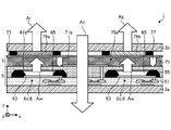
透明ディスプレイ装置1は、図1に示すように、一対のガラス基板3a及びガラス基板3bを有する。一対のガラス基板3a及びガラス基板3bは、略平行に離間して配置されている。一対のガラス基板3a及びガラス基板3bの間には、TFT(Thin Film Transistor,薄膜トランジスタ)基板5及び調光層7が設けられる。
The transparent display device 1, as shown in FIG. 1, has a pair of glass substrates 3a and 3b. A pair of the glass substrate 3a and the glass substrate 3b are spaced apart substantially in parallel. A TFT (Thin Film Transistor) substrate 5 and a light control layer 7 are provided between a pair of glass substrates 3a and 3b.
ガラス基板3aは、透明ディスプレイ装置1の裏面側に設けられる。ガラス基板3bは、透明ディスプレイ装置1の表面側に設けられる。ガラス基板3a及びガラス基板3bのそれぞれは、可視光に対して透明である。ガラス基板3a及びガラス基板3bのそれぞれは、例えば矩形の平板状の形状を有する。ここで、ガラス基板3aは、第1の基板の一例である。また、ガラス基板3bは、第2の基板の一例である。
The glass substrate 3 a is provided on the back side of the transparent display device 1 . The glass substrate 3 b is provided on the front side of the transparent display device 1 . Each of the glass substrates 3a and 3b is transparent to visible light. Each of the glass substrate 3a and the glass substrate 3b has, for example, a rectangular plate-like shape. Here, the glass substrate 3a is an example of the first substrate. Also, the glass substrate 3b is an example of a second substrate.
TFT基板5は、裏面側のガラス基板3aの表面側に設けられる。TFT基板5としては、a-Si、LTPS、IGZO等が適宜利用可能である。TFT基板5は、例えば板状の部材により形成されるが、フィルム状の部材により形成されていても構わない。TFT基板5には、複数のTFT102(図22参照)がマトリックス状に配列されている。複数のTFT102のそれぞれは、ゲート電極53a及びソース-ドレイン電極53bを有する。ソース-ドレイン電極53bは、ゲート電極53aに対応する位置の表面側に設けられている。TFT基板5において、複数のTFT102のそれぞれは、絶縁部材51により覆われている。絶縁部材51は、可視光に対して透明、かつ、電気的な絶縁性を有する材料により形成されればよい。絶縁部材51としては、例えば窒化シリコン(SiN)が利用可能である。
The TFT substrate 5 is provided on the front side of the glass substrate 3a on the back side. As the TFT substrate 5, a-Si, LTPS, IGZO, or the like can be appropriately used. The TFT substrate 5 is formed of, for example, a plate-like member, but may be formed of a film-like member. A plurality of TFTs 102 (see FIG. 22) are arranged in a matrix on the TFT substrate 5 . Each of the plurality of TFTs 102 has a gate electrode 53a and source-drain electrodes 53b. The source/drain electrodes 53b are provided on the surface side at positions corresponding to the gate electrodes 53a. In the TFT substrate 5 , each of the plurality of TFTs 102 is covered with an insulating member 51 . The insulating member 51 may be made of a material that is transparent to visible light and has electrical insulation. Silicon nitride (SiN), for example, can be used as the insulating member 51 .
TFT基板5には、複数の発光部6が設けられている。複数の発光部6のそれぞれは、透明ディスプレイ装置1の複数の発光画素100(図22参照)のそれぞれに対応する。複数の発光部6のそれぞれは、互いに独立して発光可能に構成されている。複数の発光部6のそれぞれは、絶縁部材51の内部をz-方向に延びる透明電極61aを介して、TFT102のソース-ドレイン電極53bに電気的に接続されている。透明電極61aは、可視光に対して透明な電極である。複数の発光部6のそれぞれは、例えば絶縁部材51によりTFT102とは離間している。複数の発光部6のそれぞれは、透明電極61b、反射電極63及び発光層65を有する。透明電極61b及び反射電極63は、略平行に離間して配置されている。透明電極61b及び反射電極63の間には、発光層65が設けられる。ここで、TFT基板5は、第1の内部層の一例である。
A plurality of light-emitting portions 6 are provided on the TFT substrate 5 . Each of the multiple light-emitting units 6 corresponds to each of the multiple light-emitting pixels 100 (see FIG. 22) of the transparent display device 1 . Each of the plurality of light emitting units 6 is configured to emit light independently of each other. Each of the plurality of light emitting portions 6 is electrically connected to the source-drain electrode 53b of the TFT 102 via a transparent electrode 61a extending inside the insulating member 51 in the z-direction. The transparent electrode 61a is an electrode transparent to visible light. Each of the plurality of light emitting units 6 is separated from the TFT 102 by an insulating member 51, for example. Each of the plurality of light emitting units 6 has a transparent electrode 61b, a reflective electrode 63 and a light emitting layer 65. As shown in FIG. The transparent electrode 61b and the reflective electrode 63 are arranged substantially parallel to each other. A light-emitting layer 65 is provided between the transparent electrode 61 b and the reflective electrode 63 . Here, the TFT substrate 5 is an example of the first internal layer.
透明電極61bは、複数の発光部6のそれぞれの裏面側に設けられる。透明電極61bは、透明電極61aに電気的に接続されている。透明電極61bは、可視光に対して透明である。透明電極61bは、例えば矩形の平板状の形状を有する。
The transparent electrode 61b is provided on the rear surface side of each of the plurality of light emitting units 6. The transparent electrode 61b is electrically connected to the transparent electrode 61a. The transparent electrode 61b is transparent to visible light. The transparent electrode 61b has, for example, a rectangular plate-like shape.
反射電極63は、複数の発光部6のそれぞれの表面側に設けられる。反射電極63は、透明電極61bに対向する位置に設けられている。反射電極63は、例えば透明電極61bと同様の形状を有する。反射電極63は、可視光に対して不透明である。反射電極63は、例えば金属により形成されている。あるいは、反射電極63は、表面に金属層が設けられたガラスや樹脂等により形成されている。
The reflective electrode 63 is provided on the surface side of each of the plurality of light emitting parts 6 . The reflective electrode 63 is provided at a position facing the transparent electrode 61b. The reflective electrode 63 has, for example, the same shape as the transparent electrode 61b. The reflective electrode 63 is opaque to visible light. The reflective electrode 63 is made of metal, for example. Alternatively, the reflective electrode 63 is formed of glass, resin, or the like having a metal layer on its surface.
発光層65は、有機化合物から成る発光ダイオード(LED)である。発光層65は、透明電極61b及び反射電極63の間にしきい値電圧を超える電圧が印加されると発光する。
The light emitting layer 65 is a light emitting diode (LED) made of an organic compound. The light-emitting layer 65 emits light when a voltage exceeding the threshold voltage is applied between the transparent electrode 61b and the reflective electrode 63. FIG.
複数の発光部6のそれぞれは、絶縁部材55により覆われている。絶縁部材55は、可視光に対して透明、かつ、電気的な絶縁性を有する材料により形成されればよい。絶縁部材55としては、例えば窒化シリコン(SiN)が利用可能である。
Each of the plurality of light emitting units 6 is covered with an insulating member 55. The insulating member 55 may be made of a material that is transparent to visible light and has electrical insulating properties. Silicon nitride (SiN), for example, can be used as the insulating member 55 .
TFT基板5の表面側には、調光層7が設けられている。調光層7は、透明電極71a、透明電極71b、透明電極73、調光部材75及びスペーサ77を有する。ここで、調光層7は、第2の内部層の一例である。
A dimming layer 7 is provided on the surface side of the TFT substrate 5 . The light modulating layer 7 has a transparent electrode 71 a , a transparent electrode 71 b , a transparent electrode 73 , a light modulating member 75 and a spacer 77 . Here, the light modulating layer 7 is an example of the second internal layer.
透明電極71bは、絶縁部材55の表面側に設けられる。透明電極71bは、絶縁部材51及び絶縁部材55の内部をzー方向に延びる透明電極71aを介して、TFT102のソース-ドレイン電極53bに電気的に接続されている。透明電極71bは、可視光に対して透明である。透明電極71bは、例えば矩形の平板状の形状を有する。
The transparent electrode 71 b is provided on the surface side of the insulating member 55 . The transparent electrode 71b is electrically connected to the source-drain electrode 53b of the TFT 102 via the transparent electrode 71a extending in the z-direction inside the insulating members 51 and 55. As shown in FIG. The transparent electrode 71b is transparent to visible light. The transparent electrode 71b has, for example, a rectangular plate-like shape.
透明電極73は、スペーサ77を介して、絶縁部材55の表面側に設けられる。換言すれば、透明電極73は、透明電極71bからスペーサ77のz方向の長さだけ離間して、透明電極71bと略平行に設けられている。透明電極73の表面側には、ガラス基板3aが設けられる。透明電極73は、可視光に対して透明である。透明電極73は、例えば矩形の平板状の形状を有する。
The transparent electrode 73 is provided on the surface side of the insulating member 55 via the spacer 77 . In other words, the transparent electrode 73 is spaced apart from the transparent electrode 71b by the length of the spacer 77 in the z direction and provided substantially parallel to the transparent electrode 71b. A glass substrate 3 a is provided on the surface side of the transparent electrode 73 . The transparent electrode 73 is transparent to visible light. The transparent electrode 73 has, for example, a rectangular plate-like shape.
透明電極71b及び透明電極73の間には、調光部材75が充填されている。つまり、スペーサ77は、調光部材75が充填されるギャップを透明電極71b及び透明電極73の間に形成するための部材である。調光部材75は、透明電極71b及び透明電極73の間に電圧が印加されていない状態では、可視光に対して透明である。以下、調光部材75が可視光に対して透明な状態を透過モードと記載する。調光部材75は、透明電極71b及び透明電極73の間にしきい値電圧を超える電圧が印加された状態では、透明電極71b及び透明電極73の間において可視光に対して不透明である。以下、調光部材75が可視光に対して不透明な状態を調光モードと記載する。調光部材75としては、ゲストホスト液晶、PNLC(高分子分散型液晶)、SPD(懸濁粒子)、エレクトロクロミック材料等が適宜利用可能である。なお、調光部材75は、例えば動作電圧や応答速度の特性に応じて適宜選択されればよい。例えば、調光部材75は、TFT基板5により透明電極71b及び透明電極73の間に印加された電圧に応じて透過モードと調光モードとの間で遷移する。換言すれば、調光部材75は、TFT基板5により透明電極71b及び透明電極73の間に印加された電圧に応じて可視光に対する透過率が変化する。したがって、調光部材75は、TFT基板5により駆動できる程度に、モード遷移に要求される動作電圧が低いことが好ましい。調光部材75が透明電極71b及び透明電極73によって挟まれる構造を、調光画素と称する場合がある。
A light control member 75 is filled between the transparent electrode 71b and the transparent electrode 73 . That is, the spacer 77 is a member for forming a gap between the transparent electrode 71b and the transparent electrode 73 to be filled with the light control member 75. As shown in FIG. The light control member 75 is transparent to visible light when no voltage is applied between the transparent electrode 71b and the transparent electrode 73. As shown in FIG. Hereinafter, a state in which the light control member 75 is transparent to visible light is referred to as a transmission mode. The dimming member 75 is opaque to visible light between the transparent electrodes 71b and 73 when a voltage exceeding the threshold voltage is applied between the transparent electrodes 71b and 73 . Hereinafter, a state in which the light control member 75 is opaque to visible light is referred to as a light control mode. Guest-host liquid crystal, PNLC (Polymer Dispersed Liquid Crystal), SPD (Suspended Particles), electrochromic material, or the like can be appropriately used as the light control member 75 . The light control member 75 may be appropriately selected according to, for example, characteristics such as operating voltage and response speed. For example, the light control member 75 transitions between the transmission mode and the light control mode according to the voltage applied between the transparent electrode 71b and the transparent electrode 73 by the TFT substrate 5. FIG. In other words, the light modulating member 75 changes its transmittance with respect to visible light according to the voltage applied between the transparent electrode 71b and the transparent electrode 73 by the TFT substrate 5 . Therefore, it is preferable that the light control member 75 has a low operating voltage required for mode transition to the extent that it can be driven by the TFT substrate 5 . A structure in which the light control member 75 is sandwiched between the transparent electrodes 71b and the transparent electrodes 73 is sometimes referred to as a light control pixel.
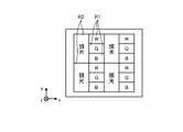
図2は、第1の実施形態に係る透明ディスプレイ装置1の構成の一例を模式的に示す平面図である。図3は、第1の実施形態に係る透明ディスプレイ装置1の構成の別の一例を模式的に示す平面図である。透明ディスプレイ装置1は、図2及び図3に示すように、発光領域R1と、調光領域R2とを有する。発光領域R1と、調光領域R2とは、図2及び図3に示すように、平面視において互いに異なる領域である。
FIG. 2 is a plan view schematically showing an example of the configuration of the transparent display device 1 according to the first embodiment. FIG. 3 is a plan view schematically showing another example of the configuration of the transparent display device 1 according to the first embodiment. The transparent display device 1, as shown in FIGS. 2 and 3, has a light emitting area R1 and a dimming area R2. As shown in FIGS. 2 and 3, the light emitting region R1 and the dimming region R2 are regions different from each other in plan view.
発光領域R1は、TFT基板5のうちの各画素が配列されている領域である。つまり、発光領域R1は、発光部6が設けられている領域である。図2は、発光領域R1にR画素、G画素及びB画素が設けられている場合を例示する。なお、発光領域R1には、図3に示すように、R画素、G画素、B画素及びW画素が設けられていてもよい。
The light emitting region R1 is a region of the TFT substrate 5 where each pixel is arranged. That is, the light emitting region R1 is a region in which the light emitting section 6 is provided. FIG. 2 illustrates a case where R pixels, G pixels, and B pixels are provided in the light emitting region R1. In addition, as shown in FIG. 3, R pixels, G pixels, B pixels, and W pixels may be provided in the light emitting region R1.
調光領域R2は、調光層7のうちの、透明電極71b及び透明電極73の間に位置する部分に対応する領域である。つまり、調光領域R2は、調光層7のうちの、透明電極71bが設けられている部分に対応する領域である。調光領域R2は、調光画素が設けられている領域でもある。ここで、調光領域R2は、平面視において、少なくともTFT基板5の各画素の間に設けられた透明領域に設けられている。より具体的には、図1に示す例では、発光部6と透明電極71bとは、平面視において互いに異なる領域である。
The light control region R2 is a region corresponding to a portion of the light control layer 7 located between the transparent electrode 71b and the transparent electrode 73. That is, the light control region R2 is a region corresponding to a portion of the light control layer 7 where the transparent electrode 71b is provided. The light control region R2 is also a region in which light control pixels are provided. Here, the dimming region R2 is provided at least in a transparent region provided between pixels of the TFT substrate 5 in plan view. More specifically, in the example shown in FIG. 1, the light emitting section 6 and the transparent electrode 71b are regions different from each other in a plan view.
次に、実施形態に係る透明ディスプレイ装置1の作用について説明する。ここでは、発光部6aは、R画素に対応し、赤色光を発生するとする。また、発光部6bは、緑色光を発生するとする。
Next, the operation of the transparent display device 1 according to the embodiment will be described. Here, it is assumed that the light emitting unit 6a corresponds to the R pixel and emits red light. It is also assumed that the light emitting unit 6b emits green light.
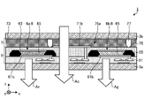
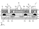
図4は、第1の実施形態に係る透明ディスプレイ装置1の透過モードにおける構成の一例を模式的に示す断面図である。発光部6aは、図4に矢印Arで示すように、発光層65からの赤色光を、裏面側に射出する。同様に、発光部6bは、図4に矢印Agで示すように、発光層65からの緑色光を、裏面側に射出する。また、透明電極71b及び透明電極73の間に電圧が印加されていない状態では、調光部材75は、可視光に対して透明である。したがって、表面側から透明ディスプレイ装置1に入射した外光Acは、透過モードの調光部材75aを透過して裏面側から射出される。なお、裏面側から透明ディスプレイ装置1に入射した外光は、透過モードの調光部材75aを透過して表面側から射出される。
FIG. 4 is a cross-sectional view schematically showing an example of the configuration of the transparent display device 1 according to the first embodiment in the transmission mode. The light-emitting portion 6a emits red light from the light-emitting layer 65 to the back side as indicated by an arrow Ar in FIG. Similarly, the light-emitting portion 6b emits green light from the light-emitting layer 65 to the back side, as indicated by an arrow Ag in FIG. In addition, when no voltage is applied between the transparent electrode 71b and the transparent electrode 73, the light control member 75 is transparent to visible light. Therefore, external light Ac entering the transparent display device 1 from the front side is transmitted through the transmission mode light control member 75a and emitted from the back side. The external light incident on the transparent display device 1 from the back side passes through the transmissive mode light control member 75a and is emitted from the front side.
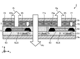
図5は、第1の実施形態に係る透明ディスプレイ装置1の調光モードにおける構成の一例を模式的に示す断面図である。発光部6a及び発光部6bは、図5に示すように、透過モードと同様に可視光を裏面側に射出する。一方で、透明電極71b及び透明電極73の間にしきい値電圧を超える電圧が印加された状態では、調光部材75は、透明電極71b及び透明電極73の間において可視光に対して不透明である。したがって、表面側から透明ディスプレイ装置1に入射した外光Acは、調光モードの調光部材75bにより遮光される。なお、裏面側から透明ディスプレイ装置1に入射した外光も、調光モードの調光部材75bにより遮光される。
FIG. 5 is a cross-sectional view schematically showing an example of the configuration in the dimming mode of the transparent display device 1 according to the first embodiment. As shown in FIG. 5, the light-emitting portions 6a and 6b emit visible light to the back side in the same manner as in the transmissive mode. On the other hand, when a voltage exceeding the threshold voltage is applied between the transparent electrode 71b and the transparent electrode 73, the light control member 75 is opaque to visible light between the transparent electrode 71b and the transparent electrode 73. . Therefore, external light Ac entering the transparent display device 1 from the surface side is blocked by the dimming member 75b in the dimming mode. It should be noted that external light entering the transparent display device 1 from the back side is also blocked by the dimming member 75b in the dimming mode.
このように、透過モードの透明ディスプレイ装置1の表示面、すなわち裏面側からは、発光部6からの光と、透明ディスプレイ装置1を透過した外光とが射出される。したがって、ユーザは、透明ディスプレイ装置1による表示とともに、透明ディスプレイ装置1の表示面とは反対側、すなわち表面側の背景の景色を見ることができる。これにより、透明ディスプレイ装置1は、例えば背景の景色に重ねて画像を表示することができる。
In this way, the light from the light emitting unit 6 and the outside light transmitted through the transparent display device 1 are emitted from the display surface of the transparent display device 1 in the transmissive mode, that is, from the back side. Therefore, the user can see the background scenery on the side opposite to the display surface of the transparent display device 1, ie, the front side, together with the display by the transparent display device 1. FIG. Thereby, the transparent display device 1 can display an image superimposed on the background scenery, for example.
このような中、発光部6からの発光に比して外光の光量が大きい環境では、透明モードの透明ディスプレイ装置1においては、表示する画像の視認性が低下する。
Under such circumstances, in an environment where the amount of external light is greater than the amount of light emitted from the light emitting unit 6, the visibility of the displayed image is reduced in the transparent display device 1 in the transparent mode.
従来、画素内に発光領域と透明領域とを有する自発光型の透明ディスプレイにおいて、その背面側に、可視光の透過率を変更する調光装置を貼り合わせる技術が知られている。しかしながら、表示エリアの全体において可視光の透過率を変更すると、表示画像以外の領域も調光されるなど、表示画像に合わせた部分的な調光ができなかった。
Conventionally, in a self-luminous transparent display having a light-emitting region and a transparent region within a pixel, a technique is known in which a dimming device for changing the transmittance of visible light is attached to the back side of the self-luminous transparent display. However, if the transmittance of visible light is changed in the entire display area, the area other than the displayed image is also dimmed.
これに対して、例えば画素単位で可視光の透過率を変更可能な調光装置を透明ディスプレイの背面側に貼り合わせる技術がある。しかしながら、貼り合わせの精度によっては、透明ディスプレイの透明画素と、調光装置の調光画素との間の位置ずれが生じてしまい、表示エリアにおける透過率のバラつきが大きくなるという問題があった。また、当該位置ずれに起因して、透明ディスプレイの格子状のパターンと、調光装置の格子状のパターンとによる回折に基づく干渉縞(モアレ)が発生するという問題があった。ここで、透明ディスプレイの格子状のパターンとは、透明ディスプレイの画素間又は発光領域と透明領域との間の構造に基づくパターンである。また、調光装置の格子状のパターンとは、調光装置の画素間の構造に基づくパターンである。また、透明ディスプレイと調光装置との間に存在する数mm程度の間隔に起因して、見る角度によって透過率が大きく変化するという問題があった。
In contrast, for example, there is a technology that attaches a light control device that can change the visible light transmittance on a pixel-by-pixel basis to the back side of a transparent display. However, depending on the accuracy of bonding, there is a problem that the transparent pixels of the transparent display and the dimming pixels of the dimming device are misaligned, resulting in large variations in transmittance in the display area. In addition, due to the positional deviation, interference fringes (moiré) are generated due to diffraction by the lattice pattern of the transparent display and the lattice pattern of the light control device. Here, the lattice pattern of the transparent display is a pattern based on the structure between the pixels of the transparent display or between the light-emitting region and the transparent region. Also, the lattice pattern of the light control device is a pattern based on the structure between the pixels of the light control device. In addition, there is a problem that the transmittance varies greatly depending on the viewing angle due to the distance of several millimeters between the transparent display and the light control device.
一方で、本実施形態に係る透明ディスプレイ装置1においては、調光層7の透明電極71bは、TFT基板5の各画素の間の領域、すなわち外光が透過可能な領域と、平面視において重複する領域に設けられている。また、ガラス基板3bの透明電極71bと対向する側には、透明電極73が設けられている。また、透明電極71b及び透明電極73の間には、透過率を変更するための液晶材料が封入されている。この構成によれば、透明電極71b及び透明電極73の間にしきい値電圧を超える電圧を印加することで、外光が透過可能な領域と平面視において重複する領域において、液晶の可視光に対する透過率を変化させることができる。
On the other hand, in the transparent display device 1 according to the present embodiment, the transparent electrode 71b of the light control layer 7 overlaps the area between the pixels of the TFT substrate 5, that is, the area through which external light can pass in plan view. It is provided in the area where A transparent electrode 73 is provided on the side of the glass substrate 3b facing the transparent electrode 71b. A liquid crystal material is sealed between the transparent electrodes 71b and 73 to change the transmittance. According to this configuration, by applying a voltage exceeding the threshold voltage between the transparent electrode 71b and the transparent electrode 73, in the region overlapping the region through which external light can be transmitted in plan view, the liquid crystal transmits visible light. You can change the rate.
このように、第1の実施形態の透明ディスプレイ装置1によれば、さらなる改善を実現できる。第1の実施形態の透明ディスプレイ装置1によれば、例えば、視認性を向上することができる。
Thus, according to the transparent display device 1 of the first embodiment, further improvements can be achieved. According to the transparent display device 1 of the first embodiment, for example, visibility can be improved.
また、本実施形態に係る透明ディスプレイ装置1においては、TFT基板5の上に調光層7が形成されている。換言すれば、TFT基板5と調光層7とは、一体に形成されている。このため、独立して形成された透明ディスプレイと調光装置とを貼り合わせる場合に比べて、TFT基板5の発光領域R1の間の透明領域と、調光層7の調光領域R2との位置ずれを抑制することができる。
Further, in the transparent display device 1 according to this embodiment, the light control layer 7 is formed on the TFT substrate 5 . In other words, the TFT substrate 5 and the light control layer 7 are integrally formed. For this reason, compared to the case where the transparent display and the light control device formed independently are bonded together, the position of the transparent region between the light emitting regions R1 of the TFT substrate 5 and the light control region R2 of the light control layer 7 is reduced. Displacement can be suppressed.
また、本実施形態に係る透明ディスプレイ装置1においては、TFT基板5と調光層7とが一体に形成されるため、TFT基板5と調光層7との間にはガラス基板を設ける必要がない。したがって、本実施形態に係る技術によれば、独立して形成された透明ディスプレイと調光装置とを貼り合わせる場合と比べて、ガラス基板の枚数を4枚から2枚に削減できるなど、薄型化及び軽量化を実現することができる。
Further, in the transparent display device 1 according to the present embodiment, the TFT substrate 5 and the light control layer 7 are integrally formed, so it is necessary to provide a glass substrate between the TFT substrate 5 and the light control layer 7. do not have. Therefore, according to the technology according to the present embodiment, compared to the case of bonding a transparent display and a light control device formed independently, the number of glass substrates can be reduced from four to two, resulting in a thinner display. And weight reduction can be realized.
(第2の実施形態)
図6は、第2の実施形態に係る透明ディスプレイ装置1の透過モードにおける構成の一例を模式的に示す断面図である。図7は、第2の実施形態に係る透明ディスプレイ装置1の調光モードにおける構成の一例を模式的に示す断面図である。 (Second embodiment)
FIG. 6 is a cross-sectional view schematically showing an example of the configuration of thetransparent display device 1 according to the second embodiment in the transmissive mode. FIG. 7 is a cross-sectional view schematically showing an example of the configuration in the dimming mode of the transparent display device 1 according to the second embodiment.
図6は、第2の実施形態に係る透明ディスプレイ装置1の透過モードにおける構成の一例を模式的に示す断面図である。図7は、第2の実施形態に係る透明ディスプレイ装置1の調光モードにおける構成の一例を模式的に示す断面図である。 (Second embodiment)
FIG. 6 is a cross-sectional view schematically showing an example of the configuration of the
本実施形態に係る透明ディスプレイ装置1の調光層7は、スペーサ77を有していなくてもよい。
The light modulating layer 7 of the transparent display device 1 according to this embodiment may not have the spacers 77 .
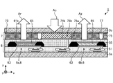
一例として、調光層7において調光部材75が充填されるギャップは、図6及び図7に示すように、TFT基板5の発光部6を覆う絶縁部材55により形成される。具体的には、透明電極71bは、絶縁部材51の表面側に設けられる。透明電極71bは、絶縁部材51の内部をz-方向に延びる透明電極71aを介して、TFT102のソース-ドレイン電極53bに電気的に接続されている。透明電極73は、絶縁部材55を介して、絶縁部材51の表面側に設けられる。換言すれば、透明電極73は、透明電極71bから発光部6を覆う絶縁部材55のz方向の長さだけ離間して、透明電極71bと略平行に設けられている。
As an example, the gap filled with the light control member 75 in the light control layer 7 is formed by an insulating member 55 covering the light emitting portion 6 of the TFT substrate 5, as shown in FIGS. Specifically, the transparent electrode 71 b is provided on the surface side of the insulating member 51 . The transparent electrode 71b is electrically connected to the source-drain electrode 53b of the TFT 102 via the transparent electrode 71a extending inside the insulating member 51 in the z-direction. The transparent electrode 73 is provided on the surface side of the insulating member 51 with the insulating member 55 interposed therebetween. In other words, the transparent electrode 73 is separated from the transparent electrode 71b by the length in the z direction of the insulating member 55 covering the light emitting section 6, and is provided substantially parallel to the transparent electrode 71b.
この構成であっても、第1の実施形態に係る透明ディスプレイ装置1と同様に、視認性を向上することができる。また、TFT基板5の絶縁部材55が設けられる層と、調光層7とが一体に形成されることから、第1の実施形態に係る透明ディスプレイ装置1と比して薄型化及び軽量化を実現することができる。
Even with this configuration, the visibility can be improved as in the transparent display device 1 according to the first embodiment. In addition, since the layer provided with the insulating member 55 of the TFT substrate 5 and the light control layer 7 are integrally formed, the thickness and weight of the transparent display device 1 can be reduced as compared with the transparent display device 1 according to the first embodiment. can be realized.
(第3の実施形態)
図8は、第3の実施形態に係る透明ディスプレイ装置1の透過モードにおける構成の一例を模式的に示す断面図である。図9は、第3の実施形態に係る透明ディスプレイ装置1の調光モードにおける構成の一例を模式的に示す断面図である。 (Third embodiment)
FIG. 8 is a cross-sectional view schematically showing an example of the configuration in the transmission mode of thetransparent display device 1 according to the third embodiment. FIG. 9 is a cross-sectional view schematically showing an example of the configuration in the dimming mode of the transparent display device 1 according to the third embodiment.
図8は、第3の実施形態に係る透明ディスプレイ装置1の透過モードにおける構成の一例を模式的に示す断面図である。図9は、第3の実施形態に係る透明ディスプレイ装置1の調光モードにおける構成の一例を模式的に示す断面図である。 (Third embodiment)
FIG. 8 is a cross-sectional view schematically showing an example of the configuration in the transmission mode of the
本実施形態に係る透明ディスプレイ装置1は、トップエミッション型の透明ディスプレイであってもよい。つまり、本実施形態に係る透明ディスプレイ装置1の表示面は、表面側に設けられる。
The transparent display device 1 according to this embodiment may be a top emission type transparent display. That is, the display surface of the transparent display device 1 according to this embodiment is provided on the front side.
透明電極61bは、図8及び図9に示すように、複数の発光部6のそれぞれの表面側に設けられる。一方で、反射電極63は、複数の発光部6のそれぞれの裏面側において、透明電極61bに対向する位置に設けられている。反射電極63は、透明電極61aに電気的に接続されている。
The transparent electrode 61b is provided on the surface side of each of the plurality of light emitting portions 6, as shown in FIGS. On the other hand, the reflective electrode 63 is provided at a position facing the transparent electrode 61b on the rear surface side of each of the plurality of light-emitting portions 6 . The reflective electrode 63 is electrically connected to the transparent electrode 61a.
発光部6aは、図8及び図9に矢印Arで示すように、発光層65からの赤色光を、表面側に射出する。同様に、発光部6bは、図8及び図9に矢印Agで示すように、発光層65からの緑色光を、表面側に射出する。また、表面側から透明ディスプレイ装置1に入射した外光Acは、透過モードの調光部材75aを透過して裏面側から射出される。一方で、表面側から透明ディスプレイ装置1に入射した外光Acは、調光モードの調光部材75bにより遮光される。
The light-emitting portion 6a emits red light from the light-emitting layer 65 to the surface side, as indicated by arrows Ar in FIGS. Similarly, the light-emitting portion 6b emits green light from the light-emitting layer 65 to the surface side, as indicated by an arrow Ag in FIGS. In addition, external light Ac entering the transparent display device 1 from the front side is transmitted through the transmission mode light control member 75a and emitted from the back side. On the other hand, external light Ac entering the transparent display device 1 from the front side is blocked by the dimming member 75b in the dimming mode.
このように、本実施形態に係る透明ディスプレイ装置1は、トップエミッション型の透明ディスプレイとして構成される。ここで、調光層7は、表示面の側に設けられている。この構成であっても、第1の実施形態に係る透明ディスプレイ装置1と同様に、視認性を向上することができる。
Thus, the transparent display device 1 according to this embodiment is configured as a top emission type transparent display. Here, the dimming layer 7 is provided on the display surface side. Even with this configuration, the visibility can be improved as in the transparent display device 1 according to the first embodiment.
なお、本実施形態に係る透明ディスプレイ装置1において、第2の実施形態に係る透明ディスプレイ装置1と同様にして、TFT基板5の絶縁部材55が設けられる層と、調光層7とが一体に形成されていてもよい。
In the transparent display device 1 according to the present embodiment, the layer provided with the insulating member 55 of the TFT substrate 5 and the light control layer 7 are integrated in the same manner as in the transparent display device 1 according to the second embodiment. may be formed.
(第4の実施形態)
図10は、第4の実施形態に係る透明ディスプレイ装置1の透過モードにおける構成の一例を模式的に示す断面図である。図11は、第4の実施形態に係る透明ディスプレイ装置1の調光モードにおける構成の一例を模式的に示す断面図である。 (Fourth embodiment)
FIG. 10 is a cross-sectional view schematically showing an example of the configuration in the transmission mode of thetransparent display device 1 according to the fourth embodiment. FIG. 11 is a cross-sectional view schematically showing an example of the configuration in the dimming mode of the transparent display device 1 according to the fourth embodiment.
図10は、第4の実施形態に係る透明ディスプレイ装置1の透過モードにおける構成の一例を模式的に示す断面図である。図11は、第4の実施形態に係る透明ディスプレイ装置1の調光モードにおける構成の一例を模式的に示す断面図である。 (Fourth embodiment)
FIG. 10 is a cross-sectional view schematically showing an example of the configuration in the transmission mode of the
本実施形態に係る複数の発光部6のそれぞれは、例えば同一の発光層65を有する。一例として、複数の発光部6cの各々は、図10及び図11に矢印Awで示すように、白色光を発生するとする。
Each of the plurality of light emitting units 6 according to this embodiment has the same light emitting layer 65, for example. As an example, it is assumed that each of the plurality of light emitting portions 6c emits white light as indicated by arrows Aw in FIGS. 10 and 11. FIG.
本実施形態に係る透明ディスプレイ装置1は、複数のカラーフィルタ79をさらに有する。複数のカラーフィルタ79のそれぞれは、透明電極73とガラス基板3bとの間に設けられる。複数のカラーフィルタ79のそれぞれは、平面視において、複数の発光部6と重複する位置に設けられる。複数のカラーフィルタ79のそれぞれは、予め定められた波長選択性を有する。カラーフィルタ79aは、例えば赤色光を透過するカラーフィルタである。カラーフィルタ79bは、例えば緑色光を透過するカラーフィルタである。
The transparent display device 1 according to this embodiment further has a plurality of color filters 79 . Each of the plurality of color filters 79 is provided between the transparent electrode 73 and the glass substrate 3b. Each of the multiple color filters 79 is provided at a position overlapping the multiple light emitting units 6 in plan view. Each of the plurality of color filters 79 has predetermined wavelength selectivity. The color filter 79a is, for example, a color filter that transmits red light. The color filter 79b is, for example, a color filter that transmits green light.
このように、本実施形態に係る透明ディスプレイ装置1において、複数の発光部6cからの白色光は、それぞれ対応するカラーフィルタ79に入射する。複数のカラーフィルタ79のそれぞれは、波長選択性に応じた波長を含む可視光を、裏面側に射出する。この構成であっても、第1の実施形態に係る透明ディスプレイ装置1と同様に、視認性を向上することができる。
As described above, in the transparent display device 1 according to this embodiment, the white light emitted from the plurality of light emitting portions 6c is incident on the corresponding color filters 79 respectively. Each of the plurality of color filters 79 emits visible light including wavelengths corresponding to wavelength selectivity to the rear surface side. Even with this configuration, the visibility can be improved as in the transparent display device 1 according to the first embodiment.
なお、複数の発光部6cの各々は、白色光に限らず、任意の波長領域の可視光を発生するOLEDであっても構わない。この場合、発光部6cからの可視光の波長領域に応じてカラーフィルタ79の波長選択性が決定されればよい。
It should be noted that each of the plurality of light-emitting portions 6c may be an OLED that emits visible light in any wavelength region, not limited to white light. In this case, the wavelength selectivity of the color filter 79 may be determined according to the wavelength range of the visible light emitted from the light emitting section 6c.
なお、本実施形態に係る透明ディスプレイ装置1は、第1の実施形態又は第2の実施形態に係る透明ディスプレイ装置1と同様にして、トップエミッション型の透明ディスプレイとして構成されていてもよい。この場合、複数のカラーフィルタ79のそれぞれは、対応する発光部6cの裏面側に設けられればよい。
Note that the transparent display device 1 according to the present embodiment may be configured as a top emission type transparent display in the same manner as the transparent display device 1 according to the first embodiment or the second embodiment. In this case, each of the plurality of color filters 79 may be provided on the back surface side of the corresponding light emitting portion 6c.
なお、本実施形態に係る透明ディスプレイ装置1において、第2の実施形態に係る透明ディスプレイ装置1と同様にして、TFT基板5の絶縁部材55が設けられる層と、調光層7とが一体に形成されていてもよい。
In the transparent display device 1 according to the present embodiment, the layer provided with the insulating member 55 of the TFT substrate 5 and the light control layer 7 are integrated in the same manner as in the transparent display device 1 according to the second embodiment. may be formed.
また、本実施形態に係る透明ディスプレイ装置1において、調光層7の調光部材75は、複数のカラーフィルタ79の間に充填されていてもよい。
Further, in the transparent display device 1 according to this embodiment, the light control member 75 of the light control layer 7 may be filled between the plurality of color filters 79 .
(第5の実施形態)
図12は、第5の実施形態に係る透明ディスプレイ装置1の透過モードにおける構成の一例を模式的に示す断面図である。図13は、第5の実施形態に係る透明ディスプレイ装置1の調光モードにおける構成の一例を模式的に示す断面図である。 (Fifth embodiment)
FIG. 12 is a cross-sectional view schematically showing an example of the configuration of thetransparent display device 1 according to the fifth embodiment in transmission mode. FIG. 13 is a cross-sectional view schematically showing an example of the configuration in the dimming mode of the transparent display device 1 according to the fifth embodiment.
図12は、第5の実施形態に係る透明ディスプレイ装置1の透過モードにおける構成の一例を模式的に示す断面図である。図13は、第5の実施形態に係る透明ディスプレイ装置1の調光モードにおける構成の一例を模式的に示す断面図である。 (Fifth embodiment)
FIG. 12 is a cross-sectional view schematically showing an example of the configuration of the
本実施形態に係る透明ディスプレイ装置1は、表面側及び裏面側の両方の側に表示面を有する透明ディスプレイであってもよい。
The transparent display device 1 according to this embodiment may be a transparent display having display surfaces on both the front side and the back side.
透明電極61bは、図12及び図13に示すように、複数の発光部6のそれぞれの裏面側に設けられる。透明電極61bは、透明電極61aに電気的に接続されている。ここで、本実施形態に係る透明ディスプレイ装置1は、反射電極63に代えて、透明電極61cを有する。透明電極61cは、複数の発光部6のそれぞれの表面側において、透明電極61bに対向する位置に設けられている。透明電極61cは、可視光に対して透明である。透明電極61cは、例えば透明電極61bと同様の形状を有する。
The transparent electrode 61b is provided on the rear surface side of each of the plurality of light emitting portions 6, as shown in FIGS. The transparent electrode 61b is electrically connected to the transparent electrode 61a. Here, the transparent display device 1 according to this embodiment has a transparent electrode 61 c instead of the reflective electrode 63 . The transparent electrode 61c is provided at a position facing the transparent electrode 61b on the surface side of each of the plurality of light emitting portions 6. As shown in FIG. The transparent electrode 61c is transparent to visible light. The transparent electrode 61c has, for example, the same shape as the transparent electrode 61b.
発光部6aは、図12及び図13に矢印Arで示すように、発光層65からの赤色光を、表面側及び裏面側の両方の側に射出する。同様に、発光部6bは、図12及び図13に矢印Agで示すように、発光層65からの緑色光を、表面側及び裏面側の両方の側に射出する。また、表面側から透明ディスプレイ装置1に入射した外光Acは、透過モードの調光部材75aを透過して裏面側から射出される。一方で、表面側から透明ディスプレイ装置1に入射した外光Acは、調光モードの調光部材75bにより遮光される。また、裏面側から透明ディスプレイ装置1に入射した外光も、調光モードの調光部材75bにより遮光される。
The light-emitting portion 6a emits red light from the light-emitting layer 65 to both the front side and the back side, as indicated by arrows Ar in FIGS. Similarly, the light-emitting portion 6b emits green light from the light-emitting layer 65 to both the front side and the back side, as indicated by arrows Ag in FIGS. In addition, external light Ac entering the transparent display device 1 from the front side is transmitted through the transmission mode light control member 75a and emitted from the back side. On the other hand, external light Ac entering the transparent display device 1 from the front side is blocked by the dimming member 75b in the dimming mode. In addition, external light entering the transparent display device 1 from the back side is also blocked by the dimming member 75b in the dimming mode.
このように、本実施形態に係る透明ディスプレイ装置1は、表面側及び裏面側の両方の側に表示面を有する透明ディスプレイとして構成される。この構成であっても、第1の実施形態に係る透明ディスプレイ装置1と同様に、視認性を向上することができる。
Thus, the transparent display device 1 according to this embodiment is configured as a transparent display having display surfaces on both the front side and the back side. Even with this configuration, the visibility can be improved as in the transparent display device 1 according to the first embodiment.
なお、本実施形態に係る透明ディスプレイ装置1において、第2の実施形態に係る透明ディスプレイ装置1と同様にして、TFT基板5の絶縁部材55が設けられる層と、調光層7とが一体に形成されていてもよい。
In the transparent display device 1 according to the present embodiment, the layer provided with the insulating member 55 of the TFT substrate 5 and the light control layer 7 are integrated in the same manner as in the transparent display device 1 according to the second embodiment. may be formed.
なお、本実施形態に係る透明ディスプレイ装置1において、第4の実施形態に係る透明ディスプレイ装置1と同様にして、複数のカラーフィルタ79が設けられていてもよい。この場合、複数のカラーフィルタ79は、透明電極73とガラス基板3bとの間に加えて、対応する発光部6cの裏面側にさらに設けられればよい。
Note that the transparent display device 1 according to this embodiment may be provided with a plurality of color filters 79 in the same manner as the transparent display device 1 according to the fourth embodiment. In this case, the plurality of color filters 79 may be provided on the rear surface side of the corresponding light emitting portion 6c in addition to between the transparent electrode 73 and the glass substrate 3b.
(第6の実施形態)
図14は、第6の実施形態に係る透明ディスプレイ装置1の透過モードにおける構成の一例を模式的に示す断面図である。図15は、第6の実施形態に係る透明ディスプレイ装置1の調光モードにおける構成の一例を模式的に示す断面図である。 (Sixth embodiment)
FIG. 14 is a cross-sectional view schematically showing an example of the configuration in the transmission mode of thetransparent display device 1 according to the sixth embodiment. FIG. 15 is a cross-sectional view schematically showing an example of the configuration in the dimming mode of the transparent display device 1 according to the sixth embodiment.
図14は、第6の実施形態に係る透明ディスプレイ装置1の透過モードにおける構成の一例を模式的に示す断面図である。図15は、第6の実施形態に係る透明ディスプレイ装置1の調光モードにおける構成の一例を模式的に示す断面図である。 (Sixth embodiment)
FIG. 14 is a cross-sectional view schematically showing an example of the configuration in the transmission mode of the
本実施形態に係る透明ディスプレイ装置1は、調光モードにおいて複数の発光部6のそれぞれからの可視光も遮光するように構成された透明ディスプレイであってもよい。
The transparent display device 1 according to this embodiment may be a transparent display configured to block visible light from each of the plurality of light emitting units 6 in the dimming mode.
透明電極71bは、図14及び図15に示すように、調光層7の全体に亘って設けられる。
The transparent electrode 71b is provided over the entire light control layer 7, as shown in FIGS.
発光部6aは、図14に矢印Arで示すように、発光層65からの赤色光を、透過モードの調光部材75aを透過させて表面側に射出する。また、発光部6aは、図14に矢印Arで示すように、発光層65からの赤色光を裏面側にも射出する。同様に、発光部6bは、図14に矢印Agで示すように、発光層65からの緑色光を、透過モードの調光部材75aを透過させて表面側に射出する。また、発光部6bは、図14に矢印Agで示すように、発光層65からの緑色光を裏面側にも射出する。また、表面側から透明ディスプレイ装置1に入射した外光Acは、透過モードの調光部材75aを透過して裏面側から射出される。
As indicated by an arrow Ar in FIG. 14, the light-emitting portion 6a transmits the red light from the light-emitting layer 65 through the transmission-mode light control member 75a and emits it to the surface side. In addition, the light-emitting portion 6a also emits red light from the light-emitting layer 65 to the back side as indicated by an arrow Ar in FIG. Similarly, the light-emitting portion 6b emits the green light from the light-emitting layer 65 to the surface side through the light control member 75a in the transmission mode, as indicated by the arrow Ag in FIG. In addition, the light-emitting portion 6b also emits green light from the light-emitting layer 65 to the back side as indicated by an arrow Ag in FIG. In addition, external light Ac entering the transparent display device 1 from the front side is transmitted through the transmission mode light control member 75a and emitted from the back side.
一方で、発光部6aから表面側へ射出される赤色光と、発光部6bから表面側へ射出される緑色光と、表面側又は裏面側から透明ディスプレイ装置1に入射した外光Acとは、それぞれ、図15に示すように、調光モードの調光部材75bにより遮光される。
On the other hand, the red light emitted from the light emitting unit 6a toward the front side, the green light emitted from the light emitting unit 6b toward the front side, and the external light Ac entering the transparent display device 1 from the front side or the back side are As shown in FIG. 15, each light is shielded by the dimming member 75b in the dimming mode.
このように、本実施形態に係る透明ディスプレイ装置1は、表面側及び裏面側の両方の側に表示面を有する透明ディスプレイとして構成される。この構成であっても、裏面側の表示面に関して、第1の実施形態に係る透明ディスプレイ装置1と同様に、視認性を向上することができる。
Thus, the transparent display device 1 according to this embodiment is configured as a transparent display having display surfaces on both the front side and the back side. Even with this configuration, the visibility of the display surface on the back side can be improved as in the case of the transparent display device 1 according to the first embodiment.
なお、本実施形態に係る透明ディスプレイ装置1において、第2の実施形態に係る透明ディスプレイ装置1と同様にして、TFT基板5の絶縁部材55が設けられる層と、調光層7とが一体に形成されていてもよい。
In the transparent display device 1 according to the present embodiment, the layer provided with the insulating member 55 of the TFT substrate 5 and the light control layer 7 are integrated in the same manner as in the transparent display device 1 according to the second embodiment. may be formed.
なお、本実施形態に係る透明ディスプレイ装置1において、第4の実施形態に係る透明ディスプレイ装置1と同様にして、複数のカラーフィルタ79が設けられていてもよい。この場合、複数のカラーフィルタ79は、透明電極73とガラス基板3bとの間に加えて、対応する発光部6cの裏面側にさらに設けられればよい。
Note that the transparent display device 1 according to this embodiment may be provided with a plurality of color filters 79 in the same manner as the transparent display device 1 according to the fourth embodiment. In this case, the plurality of color filters 79 may be provided on the rear surface side of the corresponding light emitting portion 6c in addition to between the transparent electrode 73 and the glass substrate 3b.
(第7の実施形態)
図16は、第7の実施形態に係る透明ディスプレイ装置1の透過モードにおける構成の一例を模式的に示す断面図である。図17は、第7の実施形態に係る透明ディスプレイ装置1の調光モードにおける構成の一例を模式的に示す断面図である。 (Seventh embodiment)
FIG. 16 is a cross-sectional view schematically showing an example of the configuration of thetransparent display device 1 according to the seventh embodiment in the transmissive mode. FIG. 17 is a cross-sectional view schematically showing an example of the configuration in the dimming mode of the transparent display device 1 according to the seventh embodiment.
図16は、第7の実施形態に係る透明ディスプレイ装置1の透過モードにおける構成の一例を模式的に示す断面図である。図17は、第7の実施形態に係る透明ディスプレイ装置1の調光モードにおける構成の一例を模式的に示す断面図である。 (Seventh embodiment)
FIG. 16 is a cross-sectional view schematically showing an example of the configuration of the
本実施形態に係る調光部材75は、偏光板81との組み合わせにより調光機能を有していてもよい。
The light control member 75 according to this embodiment may have a light control function in combination with the polarizing plate 81 .
本実施形態に係る透明ディスプレイ装置1は、図16及び図17に示すように、偏光板81a及び偏光板81bをさらに有する。偏光板81aは、ガラス基板3aの裏面側に設けられる。偏光板81bは、ガラス基板3bの表面側に設けられる。偏光板81a及び偏光板81bは、それぞれ、板状の部材により形成されてもよいし、フィルム状の部材により形成されてもよい。ここで、偏光板81aは、第1の偏光層の一例である。また、偏光板81bは、第2の偏光層の一例である。
The transparent display device 1 according to this embodiment further includes a polarizing plate 81a and a polarizing plate 81b, as shown in FIGS. The polarizing plate 81a is provided on the back side of the glass substrate 3a. The polarizing plate 81b is provided on the surface side of the glass substrate 3b. The polarizing plate 81a and the polarizing plate 81b may each be formed of a plate-like member, or may be formed of a film-like member. Here, the polarizing plate 81a is an example of a first polarizing layer. Also, the polarizing plate 81b is an example of a second polarizing layer.
偏光板81が設けられた透明ディスプレイ装置1では、例えばユーザが偏光サングラスを装着した状態であっても外光に起因する視認性を向上できることが好ましい。以下、調光部材75として、TN(Twisted Nematic)方式、VA(Vertical Alignment)方式及びIPS(In Plane Switching)方式の各方式の液晶が使用される場合について説明する。
In the transparent display device 1 provided with the polarizing plate 81, it is preferable that visibility due to external light can be improved even when the user is wearing polarized sunglasses, for example. A case where liquid crystals of each type of TN (Twisted Nematic) type, VA (Vertical Alignment) type, and IPS (In Plane Switching) type are used as the light control member 75 will be described below.
ここで、偏光サングラスの吸収軸は、例えば0°(水平方向)であるとする。また、透明ディスプレイ装置1においては、表面側及び裏面側の両方の側にユーザが存在する前提とする。一般に、透過型液晶ディスプレイ(LCD)では、偏光板を表裏で90°ずらして配置されている。しかしながら、偏光板の吸収軸を90°(鉛直方向)に配置すると、ディスプレイからの光は、吸収軸が0°の偏光サングラスを透過できないため、ユーザはディスプレイの表示を見ることができない。
Here, it is assumed that the absorption axis of polarized sunglasses is, for example, 0° (horizontal direction). Also, in the transparent display device 1, it is assumed that there are users on both the front side and the back side. Generally, in a transmissive liquid crystal display (LCD), polarizing plates are arranged with a 90° shift between the front and back sides. However, if the absorption axis of the polarizer is placed at 90° (vertical direction), the light from the display cannot pass through polarized sunglasses with an absorption axis of 0°, so the user cannot see the display.
そこで、本実施形態に係る透明ディスプレイ装置1では、偏光板81a及び偏光板81bは、吸収軸がともに0°になるように配置される。この構成によれば、吸収軸が0°の偏光サングラス越しの透過率を他の吸収軸の組み合わせに比して最も高くすることができる。
Therefore, in the transparent display device 1 according to this embodiment, the polarizing plates 81a and 81b are arranged so that their absorption axes are both at 0°. According to this configuration, the transmittance through polarized sunglasses having an absorption axis of 0° can be maximized compared to other combinations of absorption axes.
あるいは、本実施形態に係る透明ディスプレイ装置1では、偏光板81a及び偏光板81bは、吸収軸がともに45°になるように配置される。この場合、偏光板81aの吸収軸と、偏光板81bの吸収軸とは、90°ずらすことができる。
Alternatively, in the transparent display device 1 according to the present embodiment, the polarizing plates 81a and 81b are arranged so that their absorption axes are both at 45°. In this case, the absorption axis of the polarizing plate 81a and the absorption axis of the polarizing plate 81b can be shifted by 90°.
以下、表面側の偏光板81bの吸収軸が45°であり、かつ、裏面側の偏光板81aの吸収軸が-45°である場合を例に説明を続ける。
In the following, the case where the absorption axis of the polarizing plate 81b on the front side is 45° and the absorption axis of the polarizing plate 81a on the back side is -45° will be explained as an example.
(調光部材がTN液晶である場合)
表面側の偏光板81bに入射した非偏光の外光は、吸収軸45°の偏光板81bにより、傾き-45°の直線偏光に偏光される。ここで、透明電極71b及び透明電極73の間に電圧が印加されていない状態では、TN方式の液晶分子を90°でねじれて配向させる。液晶の位相差は、λ/2である。したがって、調光部材75を透過した光は、45°の直線偏光を有する。裏面側の偏光板81aに入射した傾き45°の直線偏光の光は、図16に示すように、吸収軸-45°の偏光板81aを透過することができる。 (When the light control member is TN liquid crystal)
The non-polarized external light incident on thepolarizing plate 81b on the front side is polarized into linearly polarized light with an inclination of -45° by the polarizing plate 81b with an absorption axis of 45°. Here, when no voltage is applied between the transparent electrodes 71b and 73, the liquid crystal molecules of the TN mode are twisted at 90° and oriented. The retardation of liquid crystal is λ/2. Therefore, the light transmitted through the dimming member 75 has linear polarization of 45°. As shown in FIG. 16, linearly polarized light with an inclination of 45° incident on the polarizing plate 81a on the back side can pass through the polarizing plate 81a with an absorption axis of −45°.
表面側の偏光板81bに入射した非偏光の外光は、吸収軸45°の偏光板81bにより、傾き-45°の直線偏光に偏光される。ここで、透明電極71b及び透明電極73の間に電圧が印加されていない状態では、TN方式の液晶分子を90°でねじれて配向させる。液晶の位相差は、λ/2である。したがって、調光部材75を透過した光は、45°の直線偏光を有する。裏面側の偏光板81aに入射した傾き45°の直線偏光の光は、図16に示すように、吸収軸-45°の偏光板81aを透過することができる。 (When the light control member is TN liquid crystal)
The non-polarized external light incident on the
一方で、透明電極71b及び透明電極73の間に電圧が印加された状態では、TN方式の液晶分子を垂直に配向させる。液晶の位相差は、0である。したがって、調光部材75を透過した光は、傾き-45°の直線偏光を有するため、図17に示すように、吸収軸-45°の偏光板81aを透過することができない。
On the other hand, when a voltage is applied between the transparent electrodes 71b and 73, the liquid crystal molecules of the TN system are vertically aligned. The phase difference of liquid crystal is zero. Therefore, the light transmitted through the light adjusting member 75 is linearly polarized with an inclination of −45°, and therefore cannot be transmitted through the polarizing plate 81a with the absorption axis of −45° as shown in FIG.
つまり、調光部材75としてTN液晶を用いる透明ディスプレイ装置1は、透明電極71b及び透明電極73の間に電圧を印加することにより、外光を遮蔽することができる。これにより、透明ディスプレイ装置1は、表示の視認性を向上することができる。
That is, the transparent display device 1 using TN liquid crystal as the light control member 75 can block external light by applying a voltage between the transparent electrode 71b and the transparent electrode 73. Thereby, the transparent display device 1 can improve the visibility of the display.
(調光部材がVA液晶である場合)
VA液晶を用いる場合、偏光板81の吸収軸を表裏ともに同じ角度に配置してノーマリーホワイトとすると、黒が沈まない、すなわちコントラストが出ないため、表裏で吸収軸を90°ずらしてノーマリーブラックとすることが好ましい。 (When the light control member is VA liquid crystal)
In the case of using VA liquid crystal, if the absorption axis of the polarizing plate 81 is arranged at the same angle on both the front and back sides to obtain normally white, the black does not sink, that is, the contrast does not appear. Black is preferred.
透明電極71b及び透明電極73の間に電圧が印加されていない状態では、VA方式の液晶分子を垂直に配向させる。液晶の位相差は、0である。したがって、調光部材75を透過した光は、傾き-45°の直線偏光を有するため、図17に示すように、吸収軸-45°の裏面側の偏光板81aを透過することができない。
When no voltage is applied between the transparent electrodes 71b and 73, the liquid crystal molecules of the VA mode are vertically aligned. The phase difference of liquid crystal is zero. Therefore, the light transmitted through the light control member 75 is linearly polarized with an inclination of −45°, and therefore cannot transmit through the polarizing plate 81a on the back side of the absorption axis of −45° as shown in FIG.
一方で、透明電極71b及び透明電極73の間に電圧が印加された状態では、VA方式の液晶分子を0°及び/又は90°方向に配向させる。液晶の位相差は、λ/2である。したがって、調光部材75を透過した光は、傾き45°の右楕円偏光及び左楕円偏光を有するため、図16に示すように、傾き45°の直線偏光の成分が吸収軸-45°の裏面側の偏光板81aを透過することができる。
On the other hand, when a voltage is applied between the transparent electrodes 71b and 73, the liquid crystal molecules of the VA mode are oriented in the 0° and/or 90° directions. The retardation of liquid crystal is λ/2. Therefore, since the light transmitted through the light control member 75 has right elliptically polarized light and left elliptical polarized light with an inclination of 45°, as shown in FIG. can be transmitted through the polarizing plate 81a on the side.
つまり、調光部材75としてVA液晶を用いる透明ディスプレイ装置1は、透明電極71b及び透明電極73の間に電圧を印加しないことにより、外光を遮蔽することができる。これにより、透明ディスプレイ装置1は、表示の視認性を向上することができる。
In other words, the transparent display device 1 using VA liquid crystal as the light control member 75 can block external light by not applying a voltage between the transparent electrode 71b and the transparent electrode 73. Thereby, the transparent display device 1 can improve the visibility of the display.
(調光部材がIPS液晶である場合)
IPS液晶を用いる場合、VA液晶を用いる場合と同様に、偏光板81の吸収軸を表裏で吸収軸を90°ずらしてノーマリーブラックとすることが好ましい。 (When the light control member is an IPS liquid crystal)
When using the IPS liquid crystal, it is preferable to shift the absorption axis of the polarizing plate 81 by 90° between the front and back surfaces to obtain normally black, as in the case of using the VA liquid crystal.
透明電極71b及び透明電極73の間に電圧が印加されていない状態では、IPS方式の液晶分子を45°に配向させる。液晶の位相差は、λ/2である。したがって、調光部材75を透過した光は、傾き-45°の直線偏光を有するため、図17に示すように、吸収軸-45°の裏面側の偏光板81aを透過することができない。
When no voltage is applied between the transparent electrodes 71b and 73, the IPS mode liquid crystal molecules are oriented at 45°. The retardation of liquid crystal is λ/2. Therefore, the light transmitted through the light control member 75 is linearly polarized with an inclination of −45°, and therefore cannot transmit through the polarizing plate 81a on the back side of the absorption axis of −45° as shown in FIG.
一方で、透明電極71b及び透明電極73の間に電圧が印加された状態では、IPS方式の液晶分子を0°及び/又は90°方向に配向させる。液晶の位相差は、λ/2である。したがって、調光部材75を透過した光は、傾き45°の右楕円偏光及び左楕円偏光を有するため、図16に示すように、傾き45°の直線偏光の成分が吸収軸-45°の裏面側の偏光板81aを透過することができる。
On the other hand, when a voltage is applied between the transparent electrodes 71b and 73, the IPS mode liquid crystal molecules are oriented in the 0° and/or 90° direction. The retardation of liquid crystal is λ/2. Therefore, since the light transmitted through the light control member 75 has right elliptically polarized light and left elliptical polarized light with an inclination of 45°, as shown in FIG. can be transmitted through the polarizing plate 81a on the side.
つまり、調光部材75としてIPS液晶を用いる透明ディスプレイ装置1は、透明電極71b及び透明電極73の間に電圧を印加しないことにより、外光を遮蔽することができる。これにより、透明ディスプレイ装置1は、表示の視認性を向上することができる。
That is, the transparent display device 1 using IPS liquid crystal as the light control member 75 can block external light by not applying a voltage between the transparent electrodes 71b and 73. Thereby, the transparent display device 1 can improve the visibility of the display.
このように、第7の実施形態に係る透明ディスプレイ装置1において、偏光板81a及び偏光板81bのそれぞれの吸収軸は、調光部材75として使用する液晶の配向に応じて規定される。したがって、本実施形態に係る技術によれば、調光部材75及び偏光板81の組み合わせにより、上述の実施形態と同様にして、画素単位の調光を実現することができる。
Thus, in the transparent display device 1 according to the seventh embodiment, the respective absorption axes of the polarizing plates 81 a and 81 b are defined according to the orientation of the liquid crystal used as the light control member 75 . Therefore, according to the technique according to the present embodiment, by combining the light control member 75 and the polarizing plate 81, it is possible to achieve light control for each pixel in the same manner as in the above-described embodiments.
なお、本実施形態に係る透明ディスプレイ装置1において、第2の実施形態に係る透明ディスプレイ装置1と同様にして、TFT基板5の絶縁部材55が設けられる層と、調光層7とが一体に形成されていてもよい。
In the transparent display device 1 according to the present embodiment, the layer provided with the insulating member 55 of the TFT substrate 5 and the light control layer 7 are integrated in the same manner as in the transparent display device 1 according to the second embodiment. may be formed.
なお、本実施形態に係る透明ディスプレイ装置1は、第3の実施形態に係る透明ディスプレイ装置1と同様にして、トップエミッション型の透明ディスプレイとして構成されていてもよい。
Note that the transparent display device 1 according to the present embodiment may be configured as a top emission type transparent display in the same manner as the transparent display device 1 according to the third embodiment.
なお、本実施形態に係る透明ディスプレイ装置1において、第4の実施形態に係る透明ディスプレイ装置1と同様にして、複数のカラーフィルタ79が設けられていてもよい。
Note that the transparent display device 1 according to this embodiment may be provided with a plurality of color filters 79 in the same manner as the transparent display device 1 according to the fourth embodiment.
なお、本実施形態に係る透明ディスプレイ装置1は、第5の実施形態又は第6の実施形態に係る透明ディスプレイ装置1と同様にして、表面側及び裏面側の両方の側に表示面を有する透明ディスプレイとして構成されていてもよい。
Note that the transparent display device 1 according to this embodiment has display surfaces on both the front side and the back side in the same manner as the transparent display device 1 according to the fifth embodiment or the sixth embodiment. It may be configured as a display.
なお、本実施形態に係る透明ディスプレイ装置1は、第6の実施形態に係る透明ディスプレイ装置1と同様にして、調光モードにおいて複数の発光部6のそれぞれからの可視光も遮光するように構成された透明ディスプレイであってもよい。
Note that the transparent display device 1 according to the present embodiment is configured to block visible light from each of the plurality of light emitting units 6 in the dimming mode in the same manner as the transparent display device 1 according to the sixth embodiment. It may also be a transparent display with a
(第8の実施形態)
図18は、第8の実施形態に係る透明ディスプレイ装置1の透過モードにおける構成の一例を模式的に示す断面図である。図19は、第8の実施形態に係る透明ディスプレイ装置1の調光モードにおける構成の一例を模式的に示す断面図である。 (Eighth embodiment)
FIG. 18 is a cross-sectional view schematically showing an example of the configuration of thetransparent display device 1 according to the eighth embodiment in transmission mode. FIG. 19 is a cross-sectional view schematically showing an example of the configuration in the dimming mode of the transparent display device 1 according to the eighth embodiment.
図18は、第8の実施形態に係る透明ディスプレイ装置1の透過モードにおける構成の一例を模式的に示す断面図である。図19は、第8の実施形態に係る透明ディスプレイ装置1の調光モードにおける構成の一例を模式的に示す断面図である。 (Eighth embodiment)
FIG. 18 is a cross-sectional view schematically showing an example of the configuration of the
本実施形態に係る調光部材75は、偏光板81及びλ/4位相差板83との組み合わせにより調光機能及び低反射機能を有していてもよい。
The light modulating member 75 according to the present embodiment may have a light modulating function and a low reflection function in combination with the polarizing plate 81 and the λ/4 retardation plate 83 .
本実施形態に係る透明ディスプレイ装置1は、図18及び図19に示すように、λ/4位相差板83a及びλ/4位相差板83bをさらに有する。λ/4位相差板83aは、ガラス基板3aと、偏光板81aとの間に設けられる。λ/4位相差板83bは、ガラス基板3bと、偏光板81bとの間に設けられる。λ/4位相差板83a及びλ/4位相差板83bは、それぞれ、板状の部材により形成されてもよいし、フィルム状の部材により形成されてもよい。ここで、λ/4位相差板83aは、第1の位相差層の一例である。また、λ/4位相差板83bは、第2の位相差層の一例である。
As shown in FIGS. 18 and 19, the transparent display device 1 according to this embodiment further includes a λ/4 retardation plate 83a and a λ/4 retardation plate 83b. The λ/4 retardation plate 83a is provided between the glass substrate 3a and the polarizing plate 81a. The λ/4 retardation plate 83b is provided between the glass substrate 3b and the polarizing plate 81b. Each of the λ/4 retardation plate 83a and the λ/4 retardation plate 83b may be formed of a plate-like member or a film-like member. Here, the λ/4 retardation plate 83a is an example of the first retardation layer. Also, the λ/4 retardation plate 83b is an example of a second retardation layer.
偏光板81が設けられた透明ディスプレイ装置1では、例えばユーザが偏光サングラスを装着した状態であっても外光に起因する視認性の低下を抑制できることが好ましい。また、TFT基板5に設けられたOLEDなどの発光部6や電極等の配線による外光の反射光に起因する視認性の低下を抑制できることがより好ましい。以下、調光部材75として、TN(Twisted Nematic)方式及びVA(Vertical Alignment)方式の各方式の液晶が使用される場合について説明する。
In the transparent display device 1 provided with the polarizing plate 81, it is preferable to be able to suppress deterioration in visibility due to external light even when the user is wearing polarized sunglasses, for example. Further, it is more preferable to be able to suppress deterioration in visibility due to reflected light of external light from the light emitting portion 6 such as an OLED provided on the TFT substrate 5 and wiring such as electrodes. A case where liquid crystals of each type of TN (Twisted Nematic) type and VA (Vertical Alignment) type are used as the light control member 75 will be described below.
λ/4位相差板83を用いる構成においては、調光部材75に入射する光、すなわちλ/4位相差板83を透過した光が円偏光となるため、液晶の配列方向を液晶の各方式について規定することが好ましい。
In the configuration using the λ/4 retardation plate 83, the light incident on the light control member 75, that is, the light transmitted through the λ/4 retardation plate 83, becomes circularly polarized light. It is preferable to define
以下、表面側及び裏面側の偏光板81a及び偏光板81bの吸収軸がともに0°であり、かつ、表面側及び裏面側のλ/4位相差板83a及びλ/4位相差板83bの遅相軸がともに45°である場合を例に説明する。
Hereinafter, the absorption axes of the polarizing plates 81a and 81b on the front and back sides are both 0°, and the λ/4 retardation plates 83a and 83b on the front and back sides are retarded. A case where both phase axes are 45° will be described as an example.
(調光部材がTN液晶である場合)
表面側の偏光板81bに入射した非偏光の外光は、吸収軸0°の偏光板81bにより、傾き90°の直線偏光に偏光された後、遅相軸45°のλ/4位相差板83bにより、左円偏光に偏光される。ここで、透明電極71b及び透明電極73の間に電圧が印加されていない状態では、TN方式の液晶分子を90°でねじれて配向させる。液晶の位相差は、λ/2である。したがって、調光部材75を透過した光は、右円偏光を有するため、傾き90°の直線偏光の成分が裏面側の遅相軸45°のλ/4位相差板83aを透過する。これにより、裏面側の偏光板81aに入射した傾き90°の直線偏光の光は、図18に示すように、吸収軸0°の偏光板81aを透過することができる。 (When the light control member is TN liquid crystal)
The unpolarized external light incident on thepolarizing plate 81b on the front side is polarized into linearly polarized light with an inclination of 90° by the polarizing plate 81b with an absorption axis of 0°, and then passes through a λ/4 retardation plate with a slow axis of 45°. 83b polarizes it to left circular polarization. Here, when no voltage is applied between the transparent electrodes 71b and 73, the liquid crystal molecules of the TN mode are twisted at 90° and oriented. The retardation of liquid crystal is λ/2. Therefore, since the light transmitted through the light control member 75 has right-handed circularly polarized light, the linearly polarized component with an inclination of 90° is transmitted through the λ/4 retardation plate 83a with a slow axis of 45° on the back side. As a result, linearly polarized light with an inclination of 90° that is incident on the polarizing plate 81a on the back side can pass through the polarizing plate 81a with an absorption axis of 0°, as shown in FIG.
表面側の偏光板81bに入射した非偏光の外光は、吸収軸0°の偏光板81bにより、傾き90°の直線偏光に偏光された後、遅相軸45°のλ/4位相差板83bにより、左円偏光に偏光される。ここで、透明電極71b及び透明電極73の間に電圧が印加されていない状態では、TN方式の液晶分子を90°でねじれて配向させる。液晶の位相差は、λ/2である。したがって、調光部材75を透過した光は、右円偏光を有するため、傾き90°の直線偏光の成分が裏面側の遅相軸45°のλ/4位相差板83aを透過する。これにより、裏面側の偏光板81aに入射した傾き90°の直線偏光の光は、図18に示すように、吸収軸0°の偏光板81aを透過することができる。 (When the light control member is TN liquid crystal)
The unpolarized external light incident on the
また、調光部材75を透過した光は、右円偏光を有する。このため、調光部材75の裏面側にあるTFT基板5において反射された光は、左円偏光を有する。したがって、調光部材75を透過した光は、右円偏光を有するため、傾き0°の直線偏光の成分が表面側の遅相軸45°のλ/4位相差板83bを透過する。これにより、表面側の遅相軸45°のλ/4位相差板83bに入射した傾き0°の直線偏光の光は、吸収軸0°の偏光板81bを透過することができない。
Also, the light transmitted through the light control member 75 has right circularly polarized light. Therefore, the light reflected by the TFT substrate 5 on the back side of the light control member 75 has left-handed circularly polarized light. Therefore, since the light transmitted through the light control member 75 has right-handed circularly polarized light, a linearly polarized component with an inclination of 0° is transmitted through the λ/4 retardation plate 83b with a slow axis of 45° on the surface side. As a result, the linearly polarized light with an inclination of 0° incident on the λ/4 retardation plate 83b with the slow axis of 45° on the front side cannot pass through the polarizing plate 81b with the absorption axis of 0°.
また、透明電極71b及び透明電極73の間に電圧が印加された状態では、TN方式の液晶分子を垂直に配向させる。液晶の位相差は、0である。したがって、調光部材75を透過した光は、左円偏光を有するため、傾き0°の直線偏光の成分が裏面側の遅相軸45°のλ/4位相差板83aを透過する。これにより、裏面側の偏光板81aに入射した傾き0°の直線偏光の光は、図19に示すように、吸収軸0°の偏光板81aを透過することができない。
Also, in a state in which a voltage is applied between the transparent electrodes 71b and 73, the liquid crystal molecules of the TN system are vertically aligned. The phase difference of liquid crystal is zero. Therefore, since the light transmitted through the light control member 75 has left-handed circularly polarized light, a linearly polarized component with an inclination of 0° is transmitted through the λ/4 retardation plate 83a with a slow axis of 45° on the back side. As a result, linearly polarized light with an inclination of 0° incident on the polarizing plate 81a on the back side cannot pass through the polarizing plate 81a with an absorption axis of 0°, as shown in FIG.
つまり、調光部材75としてTN液晶を用いる透明ディスプレイ装置1は、透明電極71b及び透明電極73の間に電圧を印加することにより、外光を遮蔽することができる。これにより、透明ディスプレイ装置1は、表示の視認性を向上することができる。また、表面側からの外光のTFT基板5による反射光が表面側に射出されることを抑制することができる。
That is, the transparent display device 1 using TN liquid crystal as the light control member 75 can block external light by applying a voltage between the transparent electrode 71b and the transparent electrode 73. Thereby, the transparent display device 1 can improve the visibility of the display. In addition, it is possible to suppress the light reflected by the TFT substrate 5 of the external light from the front surface side from being emitted to the front surface side.
なお、表面側及び裏面側のλ/4位相差板83a及びλ/4位相差板83bのうちのいずれか一方の遅相軸を-45°にすることもできる。この場合、調光部材75としてTN液晶を用いる透明ディスプレイ装置1は、透明電極71b及び透明電極73の間に電圧を印加しないことにより、外光を遮蔽することができる。これにより、透明ディスプレイ装置1は、表示の視認性を向上することができる。また、上述の場合と同様に、表面側からの外光のTFT基板5による反射光が表面側に射出されることを抑制することができる。
The slow axis of either one of the λ/4 retardation plate 83a and the λ/4 retardation plate 83b on the front side and the back side can be set to −45°. In this case, the transparent display device 1 using TN liquid crystal as the light control member 75 can block external light by not applying a voltage between the transparent electrode 71b and the transparent electrode 73. FIG. Thereby, the transparent display device 1 can improve the visibility of the display. Further, similarly to the case described above, it is possible to suppress the light reflected by the TFT substrate 5 of the external light from the front surface side from being emitted to the front surface side.
(調光部材がVA液晶である場合)
透明電極71b及び透明電極73の間に電圧が印加されていない状態では、VA方式の液晶分子を垂直に配向させる。液晶の位相差は、0である。したがって、調光部材75を透過した光は、左円偏光を有するため、傾き0°の直線偏光の成分が裏面側の遅相軸45°のλ/4位相差板83aを透過する。これにより、裏面側の偏光板81aに入射した傾き0°の直線偏光の光は、図19に示すように、吸収軸0°の偏光板81aを透過することができない。 (When the light control member is VA liquid crystal)
When no voltage is applied between the transparent electrodes 71b and 73, the VA mode liquid crystal molecules are vertically aligned. The phase difference of liquid crystal is zero. Therefore, since the light transmitted through the light control member 75 has left-handed circularly polarized light, a linearly polarized component with an inclination of 0° is transmitted through the λ/4 retardation plate 83a with a slow axis of 45° on the back side. As a result, linearly polarized light with an inclination of 0° incident on the polarizing plate 81a on the back side cannot pass through the polarizing plate 81a with an absorption axis of 0°, as shown in FIG.
透明電極71b及び透明電極73の間に電圧が印加されていない状態では、VA方式の液晶分子を垂直に配向させる。液晶の位相差は、0である。したがって、調光部材75を透過した光は、左円偏光を有するため、傾き0°の直線偏光の成分が裏面側の遅相軸45°のλ/4位相差板83aを透過する。これにより、裏面側の偏光板81aに入射した傾き0°の直線偏光の光は、図19に示すように、吸収軸0°の偏光板81aを透過することができない。 (When the light control member is VA liquid crystal)
When no voltage is applied between the
また、調光部材75を透過した光は、左円偏光を有する。このため、調光部材75の裏面側にあるTFT基板5において反射された光は、右円偏光を有する。したがって、調光部材75を透過した光は、右円偏光を有するため、傾き0°の直線偏光の成分が表面側の遅相軸45°のλ/4位相差板83bを透過する。これにより、表面側の遅相軸45°のλ/4位相差板83bに入射した傾き0°の直線偏光の光は、吸収軸0°の偏光板81bを透過することができない。
Also, the light transmitted through the light control member 75 has left circularly polarized light. Therefore, the light reflected by the TFT substrate 5 on the back side of the light control member 75 has right circularly polarized light. Therefore, since the light transmitted through the light control member 75 has right-handed circularly polarized light, a linearly polarized component with an inclination of 0° is transmitted through the λ/4 retardation plate 83b with a slow axis of 45° on the surface side. As a result, the linearly polarized light with an inclination of 0° incident on the λ/4 retardation plate 83b with the slow axis of 45° on the front side cannot pass through the polarizing plate 81b with the absorption axis of 0°.
また、透明電極71b及び透明電極73の間に電圧が印加された状態では、VA方式の液晶分子を45°及び/又は-45°に配向させる。液晶の位相差は、λ/2である。したがって、調光部材75を透過した光は、右円偏光及び左円偏光を有するため、右楕円偏光及び左楕円偏光の光が裏面側の遅相軸45°のλ/4位相差板83aを透過する。これにより、裏面側の偏光板81aに入射した右楕円偏光及び左楕円偏光の光のうち、図18に示すように、傾き90°の直線偏光の成分が吸収軸0°の偏光板81aを透過することができる。
Also, in a state in which a voltage is applied between the transparent electrodes 71b and 73, the liquid crystal molecules of the VA mode are oriented at 45° and/or -45°. The retardation of liquid crystal is λ/2. Therefore, since the light transmitted through the light control member 75 has right circularly polarized light and left circularly polarized light, the right elliptical polarized light and left elliptical polarized light pass through the λ/4 retardation plate 83a having a slow axis of 45° on the back side. To Penetrate. As a result, of the right-handed elliptically polarized light and left-handed elliptically polarized light incident on the polarizing plate 81a on the back side, as shown in FIG. can do.
つまり、調光部材75としてVA液晶を用いる透明ディスプレイ装置1は、透明電極71b及び透明電極73の間に電圧を印加しないことにより、外光を遮蔽することができる。これにより、透明ディスプレイ装置1は、表示の視認性を向上することができる。また、表面側からの外光のTFT基板5による反射光が表面側に射出されることを抑制することができる。
In other words, the transparent display device 1 using VA liquid crystal as the light control member 75 can block external light by not applying a voltage between the transparent electrode 71b and the transparent electrode 73. Thereby, the transparent display device 1 can improve the visibility of the display. In addition, it is possible to suppress the light reflected by the TFT substrate 5 of the external light from the front surface side from being emitted to the front surface side.
なお、表面側及び裏面側のλ/4位相差板83a及びλ/4位相差板83bのうちのいずれか一方の遅相軸を-45°にすることもできる。この場合、調光部材75としてVA液晶を用いる透明ディスプレイ装置1は、透明電極71b及び透明電極73の間に電圧を印加することにより、外光を遮蔽することができる。これにより、透明ディスプレイ装置1は、表示の視認性を向上することができる。また、上述の場合と同様に、表面側からの外光のTFT基板5による反射光が表面側に射出されることを抑制することができる。
The slow axis of either one of the λ/4 retardation plate 83a and the λ/4 retardation plate 83b on the front side and the back side can be set to −45°. In this case, the transparent display device 1 using VA liquid crystal as the light control member 75 can block external light by applying a voltage between the transparent electrode 71b and the transparent electrode 73. FIG. Thereby, the transparent display device 1 can improve the visibility of the display. Further, similarly to the case described above, it is possible to suppress the light reflected by the TFT substrate 5 of the external light from the front surface side from being emitted to the front surface side.
このように、第7の実施形態に係る透明ディスプレイ装置1によれば、調光部材75、偏光板81及びλ/4位相差板83の組み合わせにより、上述の実施形態と同様にして、画素単位の調光を実現することができる。また、TFT基板5における外光の反射光に起因して視認性が低下することを抑制することができる。
As described above, according to the transparent display device 1 according to the seventh embodiment, by combining the light control member 75, the polarizing plate 81 and the λ/4 retardation plate 83, the pixel unit dimming can be achieved. In addition, it is possible to suppress deterioration in visibility due to reflected light of external light on the TFT substrate 5 .
なお、本実施形態に係る透明ディスプレイ装置1において、第2の実施形態に係る透明ディスプレイ装置1と同様にして、TFT基板5の絶縁部材55が設けられる層と、調光層7とが一体に形成されていてもよい。
In the transparent display device 1 according to the present embodiment, the layer provided with the insulating member 55 of the TFT substrate 5 and the light control layer 7 are integrated in the same manner as in the transparent display device 1 according to the second embodiment. may be formed.
なお、本実施形態に係る透明ディスプレイ装置1は、第3の実施形態に係る透明ディスプレイ装置1と同様にして、トップエミッション型の透明ディスプレイとして構成されていてもよい。
Note that the transparent display device 1 according to the present embodiment may be configured as a top emission type transparent display in the same manner as the transparent display device 1 according to the third embodiment.
なお、本実施形態に係る透明ディスプレイ装置1において、第4の実施形態に係る透明ディスプレイ装置1と同様にして、複数のカラーフィルタ79が設けられていてもよい。
Note that the transparent display device 1 according to this embodiment may be provided with a plurality of color filters 79 in the same manner as the transparent display device 1 according to the fourth embodiment.
なお、本実施形態に係る透明ディスプレイ装置1は、第5の実施形態又は第6の実施形態に係る透明ディスプレイ装置1と同様にして、表面側及び裏面側の両方の側に表示面を有する透明ディスプレイとして構成されていてもよい。
Note that the transparent display device 1 according to this embodiment has display surfaces on both the front side and the back side in the same manner as the transparent display device 1 according to the fifth embodiment or the sixth embodiment. It may be configured as a display.
なお、本実施形態に係る透明ディスプレイ装置1は、第6の実施形態に係る透明ディスプレイ装置1と同様にして、調光モードにおいて複数の発光部6のそれぞれからの可視光も遮光するように構成された透明ディスプレイであってもよい。
Note that the transparent display device 1 according to the present embodiment is configured to block visible light from each of the plurality of light emitting units 6 in the dimming mode in the same manner as the transparent display device 1 according to the sixth embodiment. It may also be a transparent display with a
(第9の実施形態)
図20は、第9の実施形態に係る透明ディスプレイ装置1の透過モードにおける構成の一例を模式的に示す断面図である。図21は、第9の実施形態に係る透明ディスプレイ装置1の調光モードにおける構成の一例を模式的に示す断面図である。 (Ninth embodiment)
FIG. 20 is a cross-sectional view schematically showing an example of the configuration in the transmission mode of thetransparent display device 1 according to the ninth embodiment. FIG. 21 is a cross-sectional view schematically showing an example of the configuration in the dimming mode of the transparent display device 1 according to the ninth embodiment.
図20は、第9の実施形態に係る透明ディスプレイ装置1の透過モードにおける構成の一例を模式的に示す断面図である。図21は、第9の実施形態に係る透明ディスプレイ装置1の調光モードにおける構成の一例を模式的に示す断面図である。 (Ninth embodiment)
FIG. 20 is a cross-sectional view schematically showing an example of the configuration in the transmission mode of the
本実施形態に係る透明ディスプレイ装置1は、発光部6として、OLEDに限らず、ミニLED又はマイクロLED等のLED85を用いて構成された透明ディスプレイであってもよい。図20及び図21は、LED85としてLED85a及びLED85bを例示する。
The transparent display device 1 according to this embodiment may be a transparent display configured using LEDs 85 such as mini-LEDs or micro-LEDs, not limited to OLEDs, as the light-emitting portion 6 . 20 and 21 illustrate LED 85a and LED 85b as LED 85. FIG.
発光部6のLED85は、透明電極61b及び透明電極61cに電気的に接続される。例えば発光部6aのLED85aは、赤色発光ダイオードである。例えば発光部6bのLED85bは、緑色発光ダイオードである。
The LED 85 of the light emitting section 6 is electrically connected to the transparent electrodes 61b and 61c. For example, the LED 85a of the light emitting section 6a is a red light emitting diode. For example, the LED 85b of the light emitting section 6b is a green light emitting diode.
このように、本実施形態に係る透明ディスプレイ装置1は、発光部6として、OLEDに代えてミニLED又はマイクロLED等のLED85を有する。この構成であっても、第1の実施形態に係る透明ディスプレイ装置1と同様に、視認性を向上することができる。また、OLEDに比して焼き付きの発生を低減することができる。また、OLEDに比して発光部6の寿命を延ばすことができる。
Thus, the transparent display device 1 according to this embodiment has the LEDs 85 such as mini LEDs or micro LEDs instead of OLEDs as the light emitting section 6 . Even with this configuration, the visibility can be improved as in the transparent display device 1 according to the first embodiment. In addition, it is possible to reduce the occurrence of burn-in as compared with OLED. Moreover, the life of the light emitting part 6 can be extended compared to OLED.
なお、本実施形態に係る透明ディスプレイ装置1において、第2の実施形態に係る透明ディスプレイ装置1と同様にして、TFT基板5の絶縁部材55が設けられる層と、調光層7とが一体に形成されていてもよい。
In the transparent display device 1 according to the present embodiment, the layer provided with the insulating member 55 of the TFT substrate 5 and the light control layer 7 are integrated in the same manner as in the transparent display device 1 according to the second embodiment. may be formed.
なお、本実施形態に係る透明ディスプレイ装置1は、第3の実施形態に係る透明ディスプレイ装置1と同様にして、トップエミッション型の透明ディスプレイとして構成されていてもよい。
Note that the transparent display device 1 according to the present embodiment may be configured as a top emission type transparent display in the same manner as the transparent display device 1 according to the third embodiment.
なお、本実施形態に係る透明ディスプレイ装置1において、第4の実施形態に係る透明ディスプレイ装置1と同様にして、複数のカラーフィルタ79が設けられていてもよい。
Note that the transparent display device 1 according to this embodiment may be provided with a plurality of color filters 79 in the same manner as the transparent display device 1 according to the fourth embodiment.
なお、本実施形態に係る透明ディスプレイ装置1は、第5の実施形態又は第6の実施形態に係る透明ディスプレイ装置1と同様にして、表面側及び裏面側の両方の側に表示面を有する透明ディスプレイとして構成されていてもよい。
Note that the transparent display device 1 according to this embodiment has display surfaces on both the front side and the back side in the same manner as the transparent display device 1 according to the fifth embodiment or the sixth embodiment. It may be configured as a display.
なお、本実施形態に係る透明ディスプレイ装置1は、第6の実施形態に係る透明ディスプレイ装置1と同様にして、調光モードにおいて複数の発光部6のそれぞれからの可視光も遮光するように構成された透明ディスプレイであってもよい。
Note that the transparent display device 1 according to the present embodiment is configured to block visible light from each of the plurality of light emitting units 6 in the dimming mode in the same manner as the transparent display device 1 according to the sixth embodiment. It may also be a transparent display with a
なお、本実施形態に係る透明ディスプレイ装置1は、第7の実施形態に係る透明ディスプレイ装置1と同様にして、調光部材75及び偏光板81の組み合わせにより調光機能を実現する構成を有していてもよい。
Note that the transparent display device 1 according to the present embodiment has a configuration that realizes a light control function by combining the light control member 75 and the polarizing plate 81 in the same manner as the transparent display device 1 according to the seventh embodiment. may be
なお、本実施形態に係る透明ディスプレイ装置1は、第8の実施形態に係る透明ディスプレイ装置1と同様にして、調光部材75、偏光板81及びλ/4位相差板83の組み合わせにより調光機能及び反射低減機能を実現する構成を有していてもよい。
The transparent display device 1 according to the present embodiment is similar to the transparent display device 1 according to the eighth embodiment. You may have the structure which implement|achieves a function and a reflection reduction function.
(透明ディスプレイ装置における調光制御)
ここで、上述の各実施形態に係る透明ディスプレイ装置1における調光制御について、図面を参照しつつ、説明する。 (Dimming control in transparent display device)
Here, the light adjustment control in thetransparent display device 1 according to each of the above-described embodiments will be described with reference to the drawings.
ここで、上述の各実施形態に係る透明ディスプレイ装置1における調光制御について、図面を参照しつつ、説明する。 (Dimming control in transparent display device)
Here, the light adjustment control in the
図22は、実施形態に係る透明ディスプレイ装置1のTFT基板5の回路構成の一例を模式的に示す図である。
FIG. 22 is a diagram schematically showing an example of the circuit configuration of the TFT substrate 5 of the transparent display device 1 according to the embodiment.
TFT基板5は、図22に示すように、複数の発光画素100及び複数の調光画素110を有する。複数の発光画素100及び複数の調光画素110は、TFT基板5にマトリックス状に配列されている。複数の発光画素100は、それぞれが独立して発光可能に構成されている。複数の調光画素110は、それぞれが独立して可視光に対する透過率が変化する。複数の調光画素110は、平面視において複数の発光画素100とは異なる位置に配列されている。
The TFT substrate 5 has a plurality of light-emitting pixels 100 and a plurality of dimming pixels 110, as shown in FIG. A plurality of light-emitting pixels 100 and a plurality of dimming pixels 110 are arranged in a matrix on the TFT substrate 5 . The plurality of light-emitting pixels 100 are configured to be capable of emitting light independently. Each of the plurality of dimming pixels 110 independently changes its transmittance with respect to visible light. The plurality of dimming pixels 110 are arranged at positions different from the plurality of light emitting pixels 100 in plan view.
複数の発光画素100のそれぞれは、図22に示すように、発光素子101、TFT102、TFT105、保持容量106及び保持容量107を有する。
Each of the plurality of light emitting pixels 100 has a light emitting element 101, a TFT 102, a TFT 105, a storage capacitor 106 and a storage capacitor 107, as shown in FIG.
発光素子101のアノードは、透明電極61a及び透明電極61bを介して、TFT102のドレインに電気的に接続される。発光素子101のカソードは、反射電極63を介して、Vss側の電源配線104に電気的に接続される。発光素子101は、アノードとカソードとの間に流れる電流値に応じた輝度で発光する。
The anode of the light emitting element 101 is electrically connected to the drain of the TFT 102 via the transparent electrodes 61a and 61b. The cathode of the light emitting element 101 is electrically connected to the power supply wiring 104 on the Vss side through the reflective electrode 63 . The light-emitting element 101 emits light with luminance corresponding to the value of current flowing between the anode and the cathode.
TFT102は、発光素子101の駆動トランジスタである。TFT102は、例えばP型TFTである。TFT102のソース及びドレインは、ソース-ドレイン電極53bにより実現される。TFT102のゲートは、ゲート電極53aにより実現される。TFT102のソースは、Vdd側の電源配線103に電気的に接続される。TFT102のゲートは、TFT105のドレインに電気的に接続される。また、TFT102のゲートは、保持容量106及び保持容量107を介して、Vdd側の電源配線103に電気的に接続される。TFT102は、保持容量106及び保持容量107に保持された電圧に応じた電流を発光素子101に供給する。
A TFT 102 is a driving transistor for the light emitting element 101 . The TFT 102 is, for example, a P-type TFT. The source and drain of TFT 102 are realized by source-drain electrodes 53b. A gate of the TFT 102 is realized by a gate electrode 53a. The source of the TFT 102 is electrically connected to the power supply wiring 103 on the Vdd side. The gate of TFT 102 is electrically connected to the drain of TFT 105 . In addition, the gate of the TFT 102 is electrically connected to the power supply wiring 103 on the Vdd side through the storage capacitor 106 and the storage capacitor 107 . The TFT 102 supplies the light emitting element 101 with a current corresponding to the voltage held in the holding capacitor 106 and the holding capacitor 107 .
TFT105は、発光素子101のスイッチトランジスタである。TFT105は、例えば、P型TFTである。TFT105のソースは、映像信号線130に電気的に接続される。TFT105は、走査線駆動回路121により印加される電圧に応じてオン又はオフする。
A TFT 105 is a switch transistor of the light emitting element 101 . The TFT 105 is, for example, a P-type TFT. A source of the TFT 105 is electrically connected to the video signal line 130 . The TFT 105 is turned on or off according to the voltage applied by the scanning line driving circuit 121 .
保持容量106及び保持容量107は、TFTがオフされたときのVdd側の電源配線103の電位と、TFT102のゲートの電位との間の電位差を保持する。つまり、保持容量106及び保持容量107は、信号電圧に対応する電圧を保持する。
The holding capacitors 106 and 107 hold the potential difference between the potential of the Vdd-side power supply wiring 103 when the TFT is turned off and the potential of the gate of the TFT 102 . That is, the holding capacitors 106 and 107 hold voltages corresponding to the signal voltages.
複数の調光画素110のそれぞれは、図22に示すように、液晶素子111、TFT113、保持容量114及び保持容量115を有する。
Each of the plurality of dimming pixels 110 has a liquid crystal element 111, a TFT 113, a holding capacitor 114 and a holding capacitor 115, as shown in FIG.
液晶素子111は、調光層7の調光部材75に対応する。具体的には、調光部材75のうちの、透明電極71b及び透明電極73の間に位置する調光部材75に対応する。液晶素子111の一端は、透明電極73を介して、Vcom側の電源配線112に電気的に接続される。液晶素子111の他の一端は、TFT113のドレインに電気的に接続される。
The liquid crystal element 111 corresponds to the light modulating member 75 of the light modulating layer 7 . Specifically, it corresponds to the light control member 75 positioned between the transparent electrode 71 b and the transparent electrode 73 among the light control members 75 . One end of the liquid crystal element 111 is electrically connected to the power supply wiring 112 on the Vcom side through the transparent electrode 73 . Another end of the liquid crystal element 111 is electrically connected to the drain of the TFT 113 .
TFT113は、液晶素子111のスイッチトランジスタである。TFT113は、例えばP型TFTである。TFT113のゲート-ドレイン間には、保持容量114が電気的に接続される。TFT113は、走査線駆動回路121により印加される電圧に応じてオン又はオフする。
A TFT 113 is a switch transistor for the liquid crystal element 111 . The TFT 113 is, for example, a P-type TFT. A storage capacitor 114 is electrically connected between the gate and drain of the TFT 113 . The TFT 113 is turned on or off according to the voltage applied by the scanning line driving circuit 121 .
TFT基板5は、図22に示すように、複数の走査線120、走査線駆動回路121、複数の映像信号線130、映像信号線駆動回路131、複数の調光信号線140、調光信号線駆動回路141及び画像信号タイミング制御回路150を有する。
As shown in FIG. 22, the TFT substrate 5 includes a plurality of scanning lines 120, a scanning line driving circuit 121, a plurality of video signal lines 130, a video signal line driving circuit 131, a plurality of dimming signal lines 140, and a dimming signal line. It has a drive circuit 141 and an image signal timing control circuit 150 .
走査線駆動回路121は、複数の走査線120に電気的に接続される。図22は、複数の走査線120として、走査線Gate_n及び走査線Gate_n+1を例示する。走査線Gate_nは、複数の発光画素100のそれぞれのTFT105のゲートと、複数の調光画素110のそれぞれのTFT113のゲートとに電気的に接続される。走査線Gate_n+1は、複数の調光画素110のそれぞれの保持容量115を介して、それぞれのTFT113のドレインに電気的に接続される。走査線駆動回路121は、保持容量115を介して、TFT113のドレインに電気的に接続される。
The scanning line drive circuit 121 is electrically connected to the plurality of scanning lines 120 . FIG. 22 illustrates scanning line Gate_n and scanning line Gate_n+1 as the plurality of scanning lines 120 . The scanning line Gate_n is electrically connected to the gates of the TFTs 105 of the plurality of light-emitting pixels 100 and the gates of the TFTs 113 of the plurality of dimming pixels 110 . The scanning line Gate_n+ 1 is electrically connected to the drains of the respective TFTs 113 via the storage capacitors 115 of the plurality of dimming pixels 110 . The scanning line driving circuit 121 is electrically connected to the drain of the TFT 113 via the storage capacitor 115 .
走査線駆動回路121は、複数の走査線120に走査信号を出力することで、複数の発光画素100を順に走査する。具体的には、TFT105を行単位でオン又はオフする。これにより、走査線駆動回路121は、選択している行の複数の発光画素100に、複数の映像信号線130に映像信号線駆動回路131から出力された信号電圧を印加し、発光画素100を映像データに応じた輝度で発光させる。
The scanning line driving circuit 121 sequentially scans the plurality of luminescent pixels 100 by outputting scanning signals to the plurality of scanning lines 120 . Specifically, the TFTs 105 are turned on or off row by row. As a result, the scanning line driving circuit 121 applies the signal voltages output from the video signal line driving circuit 131 to the plurality of video signal lines 130 to the plurality of light emitting pixels 100 in the selected row, thereby turning the light emitting pixels 100 on. Light is emitted at a brightness corresponding to video data.
同様に、走査線駆動回路121は、複数の走査線120に走査信号を出力することで、複数の調光画素110を順に走査する。具体的には、TFT113を行単位でオン又はオフする。これにより、走査線駆動回路121は、選択している行の複数の調光画素110に、調光信号線駆動回路141から出力された信号電圧を印加し、調光画素110の液晶素子111の透過率を調光データに応じて変更する。
Similarly, the scanning line driving circuit 121 sequentially scans the plurality of dimming pixels 110 by outputting scanning signals to the plurality of scanning lines 120 . Specifically, the TFTs 113 are turned on or off row by row. Accordingly, the scanning line driving circuit 121 applies the signal voltage output from the dimming signal line driving circuit 141 to the plurality of dimming pixels 110 in the selected row, and the liquid crystal elements 111 of the dimming pixels 110 Transmittance is changed according to dimming data.
映像信号線駆動回路131は、複数の映像信号線130に電気的に接続される。図22は、複数の映像信号線130として、Sig_nR、Sig_nG、Sig_nB、Sig_n+1R、Sig_n+1G及びSig_n+1Bを例示する。映像信号線Sig_nRは、OLED-Rの発光画素100のTFT105のソースに電気的に接続される。映像信号線Sig_nGは、OLED-Gの発光画素100のTFT105のソースに電気的に接続される。映像信号線Sig_nBは、OLED-Bの発光画素100のTFT105のソースに電気的に接続される。ここで、OLED-Rは、赤色光を発光するOLEDである。OLED-Gは、緑色光を発光するOLEDである。OLED-Bは、青色光を発光するOLEDである。
The video signal line drive circuit 131 is electrically connected to the plurality of video signal lines 130 . FIG. 22 illustrates Sig_nR, Sig_nG, Sig_nB, Sig_n+1R, Sig_n+1G and Sig_n+1B as the plurality of video signal lines 130 . The video signal line Sig_nR is electrically connected to the source of the TFT 105 of the light emitting pixel 100 of OLED-R. The video signal line Sig_nG is electrically connected to the source of the TFT 105 of the OLED-G pixel 100 . The video signal line Sig_nB is electrically connected to the source of the TFT 105 of the light emitting pixel 100 of OLED-B. Here, OLED-R is an OLED that emits red light. OLED-G is an OLED that emits green light. OLED-B is an OLED that emits blue light.
映像信号線駆動回路131は、複数の映像信号線130を介して、映像データに対応する信号電圧を複数の発光画素100のそれぞれに印加する。
The video signal line drive circuit 131 applies signal voltages corresponding to video data to each of the plurality of light emitting pixels 100 via the plurality of video signal lines 130 .
調光信号線駆動回路141は、複数の調光信号線140に電気的に接続される。図22は、複数の調光信号線140として、調光信号線Sig_nLC及び調光信号線Sig_n+1LCを例示する。調光信号線Sig_nLC及び調光信号線Sig_n+1LCは、対応する調光画素110のTFT113のソースに電気的に接続される。
The dimming signal line drive circuit 141 is electrically connected to the multiple dimming signal lines 140 . FIG. 22 illustrates a dimming signal line Sig_nLC and a dimming signal line Sig_n+1LC as the plurality of dimming signal lines 140 . The dimming signal line Sig_nLC and the dimming signal line Sig_n+1LC are electrically connected to the source of the TFT 113 of the corresponding dimming pixel 110 .
調光信号線駆動回路141は、複数の調光信号線140を介して、調光データに対応する信号電圧を複数の調光画素110のそれぞれに印加する。
The dimming signal line drive circuit 141 applies a signal voltage corresponding to dimming data to each of the dimming pixels 110 via the dimming signal lines 140 .
画像信号タイミング制御回路150は、走査線駆動回路121、映像信号線駆動回路131及び調光信号線駆動回路141のそれぞれに電気的に接続される。画像信号タイミング制御回路150は、入力された画像信号に基づいて、走査線駆動回路121、映像信号線駆動回路131及び調光信号線駆動回路141の動作タイミングを制御する。ここで、画像信号タイミング制御回路150は、制御回路の一例である。
The image signal timing control circuit 150 is electrically connected to each of the scanning line driving circuit 121, the video signal line driving circuit 131, and the dimming signal line driving circuit 141. The image signal timing control circuit 150 controls operation timings of the scanning line driving circuit 121, the video signal line driving circuit 131, and the dimming signal line driving circuit 141 based on the inputted image signal. Here, the image signal timing control circuit 150 is an example of a control circuit.
図23は、実施形態に係る透明ディスプレイ装置1の調光制御の一例を模式的に示す信号波形図である。
FIG. 23 is a signal waveform diagram schematically showing an example of dimming control of the transparent display device 1 according to the embodiment.
画像信号タイミング制御回路150は、図23に示すように、入力された画像信号に応じたタイミングで走査線信号Vgを立ち上げるように走査線駆動回路121を制御する。走査線駆動回路121は、画像信号タイミング制御回路150の制御に従うタイミングで、例えば矩形状のパルス信号を生成し、複数の発光画素100を順に走査するとともに、複数の調光画素110を順に走査する。したがって、当該パルス信号のパルス幅は、1走査期間に相当する。
The image signal timing control circuit 150, as shown in FIG. 23, controls the scanning line driving circuit 121 so as to raise the scanning line signal Vg at a timing corresponding to the input image signal. The scanning line driving circuit 121 generates, for example, a rectangular pulse signal at a timing according to the control of the image signal timing control circuit 150, and sequentially scans the plurality of light-emitting pixels 100 and sequentially scans the plurality of dimming pixels 110. . Therefore, the pulse width of the pulse signal corresponds to one scanning period.
また、画像信号タイミング制御回路150は、入力された画像信号に基づいて、映像データに対応する信号電圧を映像信号線駆動回路131に供給するとともに、調光データに対応する信号電圧を映像信号線駆動回路131に供給する。
Based on the input image signal, the image signal timing control circuit 150 supplies the signal voltage corresponding to the video data to the video signal line driving circuit 131, and transmits the signal voltage corresponding to the dimming data to the video signal line. It is supplied to the drive circuit 131 .
ここで、画像信号タイミング制御回路150は、図23に示すように、入力された画像信号に基づいて、調光信号線駆動回路141から複数の調光画素110のそれぞれに印加される調光信号Vsigの振幅をフレームごとに制御する。
Here, as shown in FIG. 23, the image signal timing control circuit 150 controls the dimming signal applied to each of the plurality of dimming pixels 110 from the dimming signal line driving circuit 141 based on the input image signal. Control the amplitude of Vsig on a frame-by-frame basis.
このように、画像信号タイミング制御回路150は、入力された画像信号に基づいて、複数の調光画素110のそれぞれに印加される調光信号Vsigの振幅をフレームごとに制御する。換言すれば、画像信号タイミング制御回路150は、入力された画像信号に基づいて、調光画素110の液晶素子111の透過率を制御する。
Thus, the image signal timing control circuit 150 controls the amplitude of the dimming signal Vsig applied to each of the plurality of dimming pixels 110 for each frame based on the input image signal. In other words, the image signal timing control circuit 150 controls the transmittance of the liquid crystal element 111 of the dimming pixel 110 based on the input image signal.
また、画像信号タイミング制御回路150は、入力された画像信号に基づいて、走査線信号Vgが立ち上がるタイミングを制御することにより、複数の発光画素100のそれぞれの発光と、複数の調光画素110のそれぞれの調光とを制御することができる。換言すれば、画像信号タイミング制御回路150は、1つのゲートパルス信号により、透明ディスプレイ装置1における各画素の発光及び調光を制御することができる。この構成によれば、表示する画像データに応じた画素単位の調光を容易に実現することができる。
Further, the image signal timing control circuit 150 controls the timing at which the scanning line signal Vg rises based on the input image signal, so that the light emission of each of the plurality of light emitting pixels 100 and the light emission of the plurality of dimming pixels 110 are controlled. Each dimming can be controlled. In other words, the image signal timing control circuit 150 can control light emission and dimming of each pixel in the transparent display device 1 with one gate pulse signal. According to this configuration, it is possible to easily realize pixel-by-pixel light control according to image data to be displayed.
画像信号タイミング制御回路150のハードウェアとしては、例えばASIC(Application Specific Integrated Circuit)やFPGA(Field Programmable Gate Array)等のプロセッサが適宜利用可能である。
As the hardware of the image signal timing control circuit 150, for example, processors such as ASIC (Application Specific Integrated Circuit) and FPGA (Field Programmable Gate Array) can be used as appropriate.
なお、画像信号タイミング制御回路150は、例えばCPU(Central Processing Unit)等のプロセッサと、RAM(Random Access Memory)等のメモリとを有し、メモリにロードされた制御プログラムをプロセッサが実行することにより、上述の制御を実現してもよい。この場合、当該制御プログラムは、例えばROM(Read Only Memory)等に予め組み込まれて提供されてもよい。また、当該制御プログラムは、インストール可能な形式又は実行可能な形式のファイルでCD-ROM、フレキシブルディスク(FD)、CD-R、DVD(Digital Versatile Disk)等のコンピュータで読み取り可能な記録媒体に記録して提供するように構成してもよい。さらに、当該制御プログラムを、インターネット等のネットワークに接続されたコンピュータ上に格納し、ネットワーク経由でダウンロードさせることにより提供するように構成してもよい。また、当該制御プログラムをインターネット等のネットワーク経由で提供または配布するように構成してもよい。
The image signal timing control circuit 150 has a processor such as a CPU (Central Processing Unit) and a memory such as a RAM (Random Access Memory). , may implement the control described above. In this case, the control program may be provided in advance, for example, in a ROM (Read Only Memory) or the like. In addition, the control program is recorded in a computer-readable recording medium such as a CD-ROM, a flexible disk (FD), a CD-R, a DVD (Digital Versatile Disk), etc. as a file in an installable format or an executable format. may be configured to be provided as Furthermore, the control program may be stored on a computer connected to a network such as the Internet, and provided by being downloaded via the network. Also, the control program may be configured to be provided or distributed via a network such as the Internet.
本発明のいくつかの実施形態を説明したが、これらの実施形態は、例として提示したものであり、発明の範囲を限定することは意図していない。これらの実施形態は、その他の様々な形態で実施されることが可能であり、発明の要旨を逸脱しない範囲で、種々の省略、置き換え、変更を行うことができる。これらの実施形態やその変形は、発明の範囲や要旨に含まれると同様に、請求の範囲に記載された発明とその均等の範囲に含まれるものである。
Although several embodiments of the invention have been described, these embodiments are presented as examples and are not intended to limit the scope of the invention. These embodiments can be implemented in various other forms, and various omissions, replacements, and modifications can be made without departing from the scope of the invention. These embodiments and their modifications are included in the scope and spirit of the invention, as well as the scope of the invention described in the claims and equivalents thereof.
また、上記の各実施形態で説明した技術を、以下のように捉えることも可能である。
(1)
可視光を透過可能な第1の基板と、
前記第1の基板の第1の主面に設けられ、それぞれが独立して発光可能に構成された複数の発光画素と、可視光を透過可能な領域とが配列された第1の内部層と、
前記第1の内部層の前記第1の基板とは反対側に設けられ、平面視において前記複数の発光画素とは異なる位置に、それぞれが独立して可視光に対する透過率が変化する複数の調光画素が配列された第2の内部層と、
前記第2の内部層の前記第1の内部層とは反対側に設けられ、可視光を透過可能な第2の基板と
を具備する透明ディスプレイ装置。
(2)
前記第1の内部層は、前記複数の発光画素のそれぞれに電気的に接続される回路構成を有し、
前記第2の内部層は、
前記回路構成に電気的に接続され、平面視において前記複数の発光画素とは異なる位置に設けられ、可視光を透過可能な第1の電極と、
前記第2の基板の前記第1の電極と対向する側に、前記第1の電極とは離間して設けられる、可視光を透過可能な第2の電極と、
前記第1の電極と前記第2の電極との間に設けられ、前記第1の電極と前記第2の電極との間に印加された電圧に応じて可視光に対する透過率が変化する調光部材と
を有する、
上記(1)に記載の透明ディスプレイ装置。
(3)
前記複数の調光画素のそれぞれは、前記第1の内部層において、前記複数の発光画素の間に設けられる、上記(1)又は(2)に記載の透明ディスプレイ装置。
(4)
前記第1の基板の前記第1の内部層とは反対側に設けられ、可視光を偏光する第1の偏光層と、
前記第2の基板の前記第2の内部層とは反対側に設けられ、可視光を偏光する第2の偏光層と
をさらに備え、
前記複数の調光画素のそれぞれは、液晶素子を有し、
前記第1の偏光層の吸収軸と、前記第2の偏光層の吸収軸とは、前記液晶素子の配向に応じて規定される、
上記(1)から(3)のうちのいずれかに記載の透明ディスプレイ装置。
(5)
画像信号に基づいて、前記複数の発光画素及び前記複数の調光画素のそれぞれに設けられたスイッチのオン又はオフのタイミングを制御する制御回路をさらに備える、上記(1)から(4)のうちのいずれかに記載の透明ディスプレイ装置。 Also, the technology described in each of the above embodiments can be understood as follows.
(1)
a first substrate capable of transmitting visible light;
a first internal layer in which a plurality of light-emitting pixels, which are provided on the first main surface of the first substrate and configured to emit light independently, and regions capable of transmitting visible light are arranged; ,
A plurality of tone signals each independently changing transmittance with respect to visible light are provided on the side of the first inner layer opposite to the first substrate and at positions different from the plurality of light-emitting pixels in plan view. a second inner layer in which light pixels are arranged;
A transparent display device comprising: a second substrate provided on the opposite side of the second inner layer from the first inner layer and capable of transmitting visible light.
(2)
the first internal layer has a circuit configuration electrically connected to each of the plurality of light-emitting pixels;
The second inner layer comprises:
a first electrode electrically connected to the circuit configuration, provided at a position different from the plurality of light-emitting pixels in a plan view, and capable of transmitting visible light;
a second electrode capable of transmitting visible light, provided on a side of the second substrate facing the first electrode and spaced apart from the first electrode;
Dimming that is provided between the first electrode and the second electrode and has a transmittance for visible light that changes according to the voltage applied between the first electrode and the second electrode having a member and
The transparent display device according to (1) above.
(3)
The transparent display device according to (1) or (2) above, wherein each of the plurality of dimming pixels is provided between the plurality of light-emitting pixels in the first inner layer.
(4)
a first polarizing layer provided on the opposite side of the first substrate from the first inner layer for polarizing visible light;
a second polarizing layer provided on the opposite side of the second substrate from the second internal layer for polarizing visible light;
each of the plurality of dimming pixels has a liquid crystal element,
The absorption axis of the first polarizing layer and the absorption axis of the second polarizing layer are defined according to the orientation of the liquid crystal element,
The transparent display device according to any one of (1) to (3) above.
(5)
any of the above (1) to (4), further comprising a control circuit that controls on/off timing of switches provided in each of the plurality of light-emitting pixels and the plurality of dimming pixels, based on an image signal. A transparent display device according to any one of the preceding claims.
(1)
可視光を透過可能な第1の基板と、
前記第1の基板の第1の主面に設けられ、それぞれが独立して発光可能に構成された複数の発光画素と、可視光を透過可能な領域とが配列された第1の内部層と、
前記第1の内部層の前記第1の基板とは反対側に設けられ、平面視において前記複数の発光画素とは異なる位置に、それぞれが独立して可視光に対する透過率が変化する複数の調光画素が配列された第2の内部層と、
前記第2の内部層の前記第1の内部層とは反対側に設けられ、可視光を透過可能な第2の基板と
を具備する透明ディスプレイ装置。
(2)
前記第1の内部層は、前記複数の発光画素のそれぞれに電気的に接続される回路構成を有し、
前記第2の内部層は、
前記回路構成に電気的に接続され、平面視において前記複数の発光画素とは異なる位置に設けられ、可視光を透過可能な第1の電極と、
前記第2の基板の前記第1の電極と対向する側に、前記第1の電極とは離間して設けられる、可視光を透過可能な第2の電極と、
前記第1の電極と前記第2の電極との間に設けられ、前記第1の電極と前記第2の電極との間に印加された電圧に応じて可視光に対する透過率が変化する調光部材と
を有する、
上記(1)に記載の透明ディスプレイ装置。
(3)
前記複数の調光画素のそれぞれは、前記第1の内部層において、前記複数の発光画素の間に設けられる、上記(1)又は(2)に記載の透明ディスプレイ装置。
(4)
前記第1の基板の前記第1の内部層とは反対側に設けられ、可視光を偏光する第1の偏光層と、
前記第2の基板の前記第2の内部層とは反対側に設けられ、可視光を偏光する第2の偏光層と
をさらに備え、
前記複数の調光画素のそれぞれは、液晶素子を有し、
前記第1の偏光層の吸収軸と、前記第2の偏光層の吸収軸とは、前記液晶素子の配向に応じて規定される、
上記(1)から(3)のうちのいずれかに記載の透明ディスプレイ装置。
(5)
画像信号に基づいて、前記複数の発光画素及び前記複数の調光画素のそれぞれに設けられたスイッチのオン又はオフのタイミングを制御する制御回路をさらに備える、上記(1)から(4)のうちのいずれかに記載の透明ディスプレイ装置。 Also, the technology described in each of the above embodiments can be understood as follows.
(1)
a first substrate capable of transmitting visible light;
a first internal layer in which a plurality of light-emitting pixels, which are provided on the first main surface of the first substrate and configured to emit light independently, and regions capable of transmitting visible light are arranged; ,
A plurality of tone signals each independently changing transmittance with respect to visible light are provided on the side of the first inner layer opposite to the first substrate and at positions different from the plurality of light-emitting pixels in plan view. a second inner layer in which light pixels are arranged;
A transparent display device comprising: a second substrate provided on the opposite side of the second inner layer from the first inner layer and capable of transmitting visible light.
(2)
the first internal layer has a circuit configuration electrically connected to each of the plurality of light-emitting pixels;
The second inner layer comprises:
a first electrode electrically connected to the circuit configuration, provided at a position different from the plurality of light-emitting pixels in a plan view, and capable of transmitting visible light;
a second electrode capable of transmitting visible light, provided on a side of the second substrate facing the first electrode and spaced apart from the first electrode;
Dimming that is provided between the first electrode and the second electrode and has a transmittance for visible light that changes according to the voltage applied between the first electrode and the second electrode having a member and
The transparent display device according to (1) above.
(3)
The transparent display device according to (1) or (2) above, wherein each of the plurality of dimming pixels is provided between the plurality of light-emitting pixels in the first inner layer.
(4)
a first polarizing layer provided on the opposite side of the first substrate from the first inner layer for polarizing visible light;
a second polarizing layer provided on the opposite side of the second substrate from the second internal layer for polarizing visible light;
each of the plurality of dimming pixels has a liquid crystal element,
The absorption axis of the first polarizing layer and the absorption axis of the second polarizing layer are defined according to the orientation of the liquid crystal element,
The transparent display device according to any one of (1) to (3) above.
(5)
any of the above (1) to (4), further comprising a control circuit that controls on/off timing of switches provided in each of the plurality of light-emitting pixels and the plurality of dimming pixels, based on an image signal. A transparent display device according to any one of the preceding claims.
1 透明ディスプレイ装置
3a,3b ガラス基板
5 TFT基板
51 絶縁部材
53a ゲート電極
53b ソース-ドレイン電極
55 絶縁部材
6,6a,6b,6c 発光部
61a,61b,61c 透明電極
63 反射電極
65 発光層
7 調光層
71a,71b,73 透明電極
75 調光部材
77 スペーサ
79a,79b カラーフィルタ
81a,81b 偏光板
83a,83b λ/4位相差板
85,85a,85b LED
100 発光画素
101 発光素子
102,105,113 TFT
106,107,114,115 保持容量
110 調光画素
111 液晶素子
120 走査線
121 走査線駆動回路
130 映像信号線
131 映像信号線駆動回路
140 調光信号線
141 調光信号線駆動回路
150 画像信号タイミング制御回路
R1 発光領域
R2 調光領域 1 transparent display device 3a, 3b glass substrate 5 TFT substrate 51 insulating member 53a gate electrode 53b source-drain electrode 55 insulating member 6, 6a, 6b, 6c light emitting section 61a, 61b, 61c transparent electrode 63 reflective electrode 65 light emitting layer 7 tone Optical layer 71a, 71b, 73 Transparent electrode 75 Light control member 77 Spacer 79a, 79b Color filter 81a, 81b Polarizing plate 83a, 83b λ/4 retardation plate 85, 85a, 85b LED
100light emitting pixel 101 light emitting element 102, 105, 113 TFT
106, 107, 114, 115storage capacitor 110 dimming pixel 111 liquid crystal element 120 scanning line 121 scanning line driving circuit 130 video signal line 131 video signal line driving circuit 140 dimming signal line 141 dimming signal line driving circuit 150 image signal timing Control circuit R1 light emitting area R2 dimming area
3a,3b ガラス基板
5 TFT基板
51 絶縁部材
53a ゲート電極
53b ソース-ドレイン電極
55 絶縁部材
6,6a,6b,6c 発光部
61a,61b,61c 透明電極
63 反射電極
65 発光層
7 調光層
71a,71b,73 透明電極
75 調光部材
77 スペーサ
79a,79b カラーフィルタ
81a,81b 偏光板
83a,83b λ/4位相差板
85,85a,85b LED
100 発光画素
101 発光素子
102,105,113 TFT
106,107,114,115 保持容量
110 調光画素
111 液晶素子
120 走査線
121 走査線駆動回路
130 映像信号線
131 映像信号線駆動回路
140 調光信号線
141 調光信号線駆動回路
150 画像信号タイミング制御回路
R1 発光領域
R2 調光領域 1
100
106, 107, 114, 115
Claims (20)
- 可視光を透過可能な第1の基板と、
前記第1の基板の主面に設けられ、
それぞれが独立して発光可能に構成された複数の発光画素と、
それぞれが独立して可視光に対する透過率が変化する複数の調光画素と
が、平面視において異なる位置に配列された内部層と、
前記内部層の前記第1の基板とは反対側に設けられ、可視光を透過可能な第2の基板と
を具備する透明ディスプレイ装置。 a first substrate capable of transmitting visible light;
provided on the main surface of the first substrate,
a plurality of light-emitting pixels each configured to emit light independently;
an internal layer in which a plurality of dimming pixels, each of which independently changes its transmittance with respect to visible light, are arranged at different positions in plan view;
A transparent display device comprising: a second substrate provided on the inner layer opposite the first substrate and capable of transmitting visible light. - 前記内部層は、
前記第1の基板の側に設けられ、前記複数の発光画素と、可視光を透過可能な領域とが配列された第1の内部層と、
前記第2の基板の側に設けられ、前記可視光を透過可能な領域に対応する位置に前記複数の調光画素が配列された第2の内部層と
を有する、請求項1に記載の透明ディスプレイ装置。 The inner layer comprises
a first internal layer provided on the first substrate side, in which the plurality of light-emitting pixels and regions capable of transmitting visible light are arranged;
2. The transparent according to claim 1, further comprising: a second internal layer provided on the second substrate side and having the plurality of dimming pixels arranged at positions corresponding to the regions capable of transmitting visible light. display device. - 前記第1の内部層は、前記複数の発光画素のそれぞれに電気的に接続される回路構成を有し、
前記第2の内部層は、
前記回路構成に電気的に接続され、平面視において前記複数の発光画素とは異なる位置に設けられ、可視光を透過可能な第1の電極と、
前記第2の基板の前記第1の電極と対向する側に、前記第1の電極とは離間して設けられる、可視光を透過可能な第2の電極と、
前記第1の電極と前記第2の電極との間に設けられ、前記第1の電極と前記第2の電極との間に印加された電圧に応じて可視光に対する透過率が変化する調光部材と
を有する、
請求項2に記載の透明ディスプレイ装置。 the first internal layer has a circuit configuration electrically connected to each of the plurality of light-emitting pixels;
The second inner layer comprises:
a first electrode electrically connected to the circuit configuration, provided at a position different from the plurality of light-emitting pixels in a plan view, and capable of transmitting visible light;
a second electrode capable of transmitting visible light, provided on a side of the second substrate facing the first electrode and spaced apart from the first electrode;
Dimming that is provided between the first electrode and the second electrode and has a transmittance for visible light that changes according to the voltage applied between the first electrode and the second electrode having a member and
3. The transparent display device of claim 2. - 前記複数の調光画素のそれぞれは、前記内部層において、前記複数の発光画素の間に設けられる、請求項1又は請求項2に記載の透明ディスプレイ装置。 3. The transparent display device according to claim 1, wherein each of said plurality of dimming pixels is provided between said plurality of luminescent pixels in said inner layer.
- 前記内部層は、
前記複数の発光画素のそれぞれに電気的に接続される回路構成と、
前記回路構成に電気的に接続され、平面視において前記複数の発光画素とは異なる位置に設けられ、可視光を透過可能な第1の電極と、
前記第2の基板の前記第1の電極と対向する側に、前記第1の電極とは離間して設けられる、可視光を透過可能な第2の電極と、
前記第1の電極と前記第2の電極との間に設けられ、前記第1の電極と前記第2の電極との間に印加された電圧に応じて可視光に対する透過率が変化する調光部材と
を有する、
請求項4に記載の透明ディスプレイ装置。 The inner layer comprises
a circuit configuration electrically connected to each of the plurality of light emitting pixels;
a first electrode electrically connected to the circuit configuration, provided at a position different from the plurality of light-emitting pixels in a plan view, and capable of transmitting visible light;
a second electrode capable of transmitting visible light, provided on a side of the second substrate facing the first electrode and spaced apart from the first electrode;
Dimming that is provided between the first electrode and the second electrode and has a transmittance for visible light that changes according to the voltage applied between the first electrode and the second electrode having a member and
5. The transparent display device of claim 4. - 前記第1の電極は、前記複数の調光画素それぞれに設けられる、請求項3又は請求項5に記載の透明ディスプレイ装置。 6. The transparent display device according to claim 3, wherein the first electrode is provided for each of the plurality of dimming pixels.
- 前記第1の電極は、前記複数の調光画素それぞれに設けられ、前記複数の発光画素のうちの隣接する発光画素を覆う位置まで延びる、請求項3又は請求項5に記載の透明ディスプレイ装置。 6. The transparent display device according to claim 3, wherein the first electrode is provided for each of the plurality of dimming pixels and extends to a position covering an adjacent luminescent pixel among the plurality of luminescent pixels.
- 前記複数の発光画素それぞれの発光面は、前記第1の基板に対向する側に設けられている、請求項1から請求項6のうちのいずれか一項に記載の透明ディスプレイ装置。 The transparent display device according to any one of claims 1 to 6, wherein the light emitting surface of each of the plurality of light emitting pixels is provided on the side facing the first substrate.
- 前記複数の発光画素それぞれの発光面と前記第1の基板との間に設けられ、それぞれが予め定められた波長選択性を有する複数のカラーフィルタをさらに備える、請求項8に記載の透明ディスプレイ装置。 9. The transparent display device of claim 8, further comprising a plurality of color filters provided between the light emitting surface of each of the plurality of light emitting pixels and the first substrate, each having a predetermined wavelength selectivity. .
- 前記複数の発光画素それぞれの発光面は、前記第2の基板に対向する側に設けられている、請求項1から請求項6のうちのいずれか一項に記載の透明ディスプレイ装置。 The transparent display device according to any one of claims 1 to 6, wherein the light emitting surface of each of the plurality of light emitting pixels is provided on the side facing the second substrate.
- 前記複数の発光画素それぞれの発光面と前記第2の基板との間に設けられ、それぞれが予め定められた波長選択性を有する複数のカラーフィルタをさらに備える、請求項10に記載の透明ディスプレイ装置。 11. The transparent display device of claim 10, further comprising a plurality of color filters provided between the light emitting surface of each of the plurality of light emitting pixels and the second substrate, each having a predetermined wavelength selectivity. .
- 前記複数のカラーフィルタそれぞれは、前記第2の基板と前記内部層との間に設けられている、請求項11に記載の透明ディスプレイ装置。 12. The transparent display device according to claim 11, wherein each of said plurality of color filters is provided between said second substrate and said inner layer.
- 前記複数の発光画素それぞれの発光面は、前記第1の基板に対向する側及び前記第2の基板に対向する側それぞれに設けられている、請求項1から請求項7のうちのいずれか一項に記載の透明ディスプレイ装置。 8. The light-emitting surface of each of the plurality of light-emitting pixels is provided on a side facing the first substrate and on a side facing the second substrate. A transparent display device according to any one of claims 1 to 3.
- 前記第1の基板の前記内部層とは反対側に設けられ、可視光を偏光する第1の偏光層と、
前記第2の基板の前記内部層とは反対側に設けられ、可視光を偏光する第2の偏光層と
をさらに備え、
前記複数の調光画素のそれぞれは、液晶素子を有し、
前記第1の偏光層の吸収軸と、前記第2の偏光層の吸収軸とは、前記液晶素子の配向に応じて規定される、
請求項1から請求項13のうちのいずれか一項に記載の透明ディスプレイ装置。 a first polarizing layer provided on the opposite side of the first substrate from the internal layer for polarizing visible light;
a second polarizing layer that is provided on the opposite side of the second substrate from the internal layer and that polarizes visible light;
Each of the plurality of dimming pixels has a liquid crystal element,
The absorption axis of the first polarizing layer and the absorption axis of the second polarizing layer are defined according to the orientation of the liquid crystal element,
14. A transparent display device according to any one of claims 1 to 13. - 前記液晶素子は、TN液晶、VS液晶及びIPS液晶のうちのいずれかである、請求項14に記載の透明ディスプレイ装置。 15. The transparent display device according to claim 14, wherein the liquid crystal element is one of TN liquid crystal, VS liquid crystal and IPS liquid crystal.
- 前記第1の偏光層及び前記第2の偏光層の吸収軸は、一方が45°であり、かつ、他方が-45°である、請求項14又は請求項15に記載の透明ディスプレイ装置。 The transparent display device according to claim 14 or 15, wherein one of the absorption axes of the first polarizing layer and the second polarizing layer is 45° and the other is -45°.
- 前記第1の偏光層と前記第1の基板との間に設けられた第1の位相差層と、
前記第2の偏光層と前記第2の基板との間に設けられた第2の位相差層と
をさらに備える、請求項14に記載の透明ディスプレイ装置。 a first retardation layer provided between the first polarizing layer and the first substrate;
15. The transparent display device of Claim 14, further comprising: a second retardation layer provided between said second polarizing layer and said second substrate. - 前記液晶素子は、TN液晶又はVS液晶である、請求項17に記載の透明ディスプレイ装置。 The transparent display device according to claim 17, wherein the liquid crystal element is TN liquid crystal or VS liquid crystal.
- 前記第1の偏光層及び前記第2の偏光層の吸収軸は、それぞれ0°であり、
前記第1の位相差層及び前記第2の位相差層のうちの少なくとも一方の遅相軸は、45°である、
請求項17又は請求項18に記載の透明ディスプレイ装置。 The absorption axes of the first polarizing layer and the second polarizing layer are each 0°,
At least one of the first retardation layer and the second retardation layer has a slow axis of 45°,
19. A transparent display device according to claim 17 or 18. - 画像信号に基づいて、前記複数の発光画素及び前記複数の調光画素のそれぞれに設けられたスイッチのオン又はオフのタイミングを制御する制御回路をさらに備える、請求項1から請求項19のうちのいずれか一項に記載の透明ディスプレイ装置。 20. Any one of claims 1 to 19, further comprising a control circuit that controls on/off timing of switches provided in each of the plurality of light-emitting pixels and the plurality of dimming pixels based on an image signal. A transparent display device according to any one of the preceding claims.
Priority Applications (2)
| Application Number | Priority Date | Filing Date | Title |
|---|---|---|---|
| JP2023505190A JPWO2022190688A1 (en) | 2021-03-11 | 2022-01-26 | |
| US18/238,306 US20230413641A1 (en) | 2021-03-11 | 2023-08-25 | Transparent display device |
Applications Claiming Priority (2)
| Application Number | Priority Date | Filing Date | Title |
|---|---|---|---|
| JP2021039661 | 2021-03-11 | ||
| JP2021-039661 | 2021-03-11 |
Related Child Applications (1)
| Application Number | Title | Priority Date | Filing Date |
|---|---|---|---|
| US18/238,306 Continuation US20230413641A1 (en) | 2021-03-11 | 2023-08-25 | Transparent display device |
Publications (1)
| Publication Number | Publication Date |
|---|---|
| WO2022190688A1 true WO2022190688A1 (en) | 2022-09-15 |
Family
ID=83226729
Family Applications (1)
| Application Number | Title | Priority Date | Filing Date |
|---|---|---|---|
| PCT/JP2022/002954 WO2022190688A1 (en) | 2021-03-11 | 2022-01-26 | Transparent display device |
Country Status (3)
| Country | Link |
|---|---|
| US (1) | US20230413641A1 (en) |
| JP (1) | JPWO2022190688A1 (en) |
| WO (1) | WO2022190688A1 (en) |
Families Citing this family (1)
| Publication number | Priority date | Publication date | Assignee | Title |
|---|---|---|---|---|
| CN113097243A (en) * | 2021-03-31 | 2021-07-09 | 京东方科技集团股份有限公司 | Micro light-emitting diode chip, display substrate, manufacturing method of micro light-emitting diode chip and display device |
Citations (6)
| Publication number | Priority date | Publication date | Assignee | Title |
|---|---|---|---|---|
| JP2007042612A (en) * | 2005-06-29 | 2007-02-15 | Hitachi Displays Ltd | Organic electroluminescence display device and manufacturing method thereof |
| US20150168776A1 (en) * | 2013-12-18 | 2015-06-18 | Samsung Display Co., Ltd. | Display device for controlling light transmittance |
| US20160197131A1 (en) * | 2015-01-02 | 2016-07-07 | Samsung Display Co., Ltd. | Transparent display device and method of manufacturing the same |
| JP2016184175A (en) * | 2011-01-07 | 2016-10-20 | 株式会社半導体エネルギー研究所 | Display device |
| JP2019153411A (en) * | 2018-03-01 | 2019-09-12 | セイコーエプソン株式会社 | Electro-optical device, method of manufacturing the same, and electronic apparatus |
| WO2020111101A1 (en) * | 2018-11-30 | 2020-06-04 | ソニー株式会社 | Display device |
-
2022
- 2022-01-26 JP JP2023505190A patent/JPWO2022190688A1/ja active Pending
- 2022-01-26 WO PCT/JP2022/002954 patent/WO2022190688A1/en active Application Filing
-
2023
- 2023-08-25 US US18/238,306 patent/US20230413641A1/en active Pending
Patent Citations (6)
| Publication number | Priority date | Publication date | Assignee | Title |
|---|---|---|---|---|
| JP2007042612A (en) * | 2005-06-29 | 2007-02-15 | Hitachi Displays Ltd | Organic electroluminescence display device and manufacturing method thereof |
| JP2016184175A (en) * | 2011-01-07 | 2016-10-20 | 株式会社半導体エネルギー研究所 | Display device |
| US20150168776A1 (en) * | 2013-12-18 | 2015-06-18 | Samsung Display Co., Ltd. | Display device for controlling light transmittance |
| US20160197131A1 (en) * | 2015-01-02 | 2016-07-07 | Samsung Display Co., Ltd. | Transparent display device and method of manufacturing the same |
| JP2019153411A (en) * | 2018-03-01 | 2019-09-12 | セイコーエプソン株式会社 | Electro-optical device, method of manufacturing the same, and electronic apparatus |
| WO2020111101A1 (en) * | 2018-11-30 | 2020-06-04 | ソニー株式会社 | Display device |
Also Published As
| Publication number | Publication date |
|---|---|
| JPWO2022190688A1 (en) | 2022-09-15 |
| US20230413641A1 (en) | 2023-12-21 |
Similar Documents
| Publication | Publication Date | Title |
|---|---|---|
| JP7138742B2 (en) | liquid crystal display | |
| US10754186B2 (en) | Display device and display method | |
| KR101774678B1 (en) | Liquid crystal display device | |
| JP4407690B2 (en) | Liquid crystal display | |
| WO2016171096A1 (en) | Liquid crystal display device | |
| JP7182906B2 (en) | Display devices and electronic devices | |
| CN109073921B (en) | Switch type mirror panel and switch type mirror device | |
| WO2015190588A1 (en) | Liquid crystal display device | |
| US20230413641A1 (en) | Transparent display device | |
| WO2020230570A1 (en) | Display device | |
| TWI308307B (en) | Image display system | |
| US20220365389A1 (en) | Electronic device | |
| JP2023120988A (en) | Display apparatus | |
| US10942363B2 (en) | Liquid crystal display device | |
| KR102455577B1 (en) | Flat display device | |
| KR20080073672A (en) | Liquid crystal display device and electronic apparatus including the same | |
| KR101274027B1 (en) | Display panel and display apparatus having the same | |
| WO2022210082A1 (en) | Display device | |
| WO2024084680A1 (en) | Display device | |
| KR20130033618A (en) | Transparent liquid crystal display device | |
| US11852939B2 (en) | Display device and electronic device | |
| US20230305339A1 (en) | Image output panel and head-up display | |
| US11960166B2 (en) | Display device | |
| JP2024054567A (en) | Display device | |
| JP4947042B2 (en) | Driving method of transflective liquid crystal display device |
Legal Events
| Date | Code | Title | Description |
|---|---|---|---|
| 121 | Ep: the epo has been informed by wipo that ep was designated in this application |
Ref document number: 22766655 Country of ref document: EP Kind code of ref document: A1 |
|
| WWE | Wipo information: entry into national phase |
Ref document number: 2023505190 Country of ref document: JP |
|
| NENP | Non-entry into the national phase |
Ref country code: DE |
|
| 122 | Ep: pct application non-entry in european phase |
Ref document number: 22766655 Country of ref document: EP Kind code of ref document: A1 |