WO2022176736A1 - Display device - Google Patents
Display device Download PDFInfo
- Publication number
- WO2022176736A1 WO2022176736A1 PCT/JP2022/005126 JP2022005126W WO2022176736A1 WO 2022176736 A1 WO2022176736 A1 WO 2022176736A1 JP 2022005126 W JP2022005126 W JP 2022005126W WO 2022176736 A1 WO2022176736 A1 WO 2022176736A1
- Authority
- WO
- WIPO (PCT)
- Prior art keywords
- layer
- lower electrode
- organic layer
- opening
- display device
- Prior art date
Links
- 239000010410 layer Substances 0.000 claims abstract description 170
- 239000012044 organic layer Substances 0.000 claims abstract description 58
- 230000002093 peripheral effect Effects 0.000 claims abstract description 44
- 238000005192 partition Methods 0.000 claims abstract description 35
- 239000000758 substrate Substances 0.000 claims abstract description 15
- 239000002346 layers by function Substances 0.000 claims description 13
- 230000000903 blocking effect Effects 0.000 claims description 7
- 239000000463 material Substances 0.000 claims description 7
- 238000000638 solvent extraction Methods 0.000 claims description 3
- 238000005401 electroluminescence Methods 0.000 description 71
- 230000004048 modification Effects 0.000 description 13
- 238000012986 modification Methods 0.000 description 13
- 239000003086 colorant Substances 0.000 description 8
- 230000000052 comparative effect Effects 0.000 description 8
- 238000010586 diagram Methods 0.000 description 7
- 239000010408 film Substances 0.000 description 7
- 230000006866 deterioration Effects 0.000 description 5
- 230000000694 effects Effects 0.000 description 5
- 229910052581 Si3N4 Inorganic materials 0.000 description 4
- 229910052751 metal Inorganic materials 0.000 description 4
- 239000002184 metal Substances 0.000 description 4
- HQVNEWCFYHHQES-UHFFFAOYSA-N silicon nitride Chemical compound N12[Si]34N5[Si]62N3[Si]51N64 HQVNEWCFYHHQES-UHFFFAOYSA-N 0.000 description 4
- 230000015572 biosynthetic process Effects 0.000 description 3
- 239000003990 capacitor Substances 0.000 description 3
- 230000005525 hole transport Effects 0.000 description 3
- 238000002347 injection Methods 0.000 description 3
- 239000007924 injection Substances 0.000 description 3
- 238000000034 method Methods 0.000 description 3
- BQCADISMDOOEFD-UHFFFAOYSA-N Silver Chemical compound [Ag] BQCADISMDOOEFD-UHFFFAOYSA-N 0.000 description 2
- 229910052782 aluminium Inorganic materials 0.000 description 2
- XAGFODPZIPBFFR-UHFFFAOYSA-N aluminium Chemical compound [Al] XAGFODPZIPBFFR-UHFFFAOYSA-N 0.000 description 2
- 239000004020 conductor Substances 0.000 description 2
- 239000011810 insulating material Substances 0.000 description 2
- 239000011777 magnesium Substances 0.000 description 2
- 238000004519 manufacturing process Methods 0.000 description 2
- 239000007769 metal material Substances 0.000 description 2
- 229910052709 silver Inorganic materials 0.000 description 2
- 239000004332 silver Substances 0.000 description 2
- 239000010936 titanium Substances 0.000 description 2
- 239000004925 Acrylic resin Substances 0.000 description 1
- 229920000178 Acrylic resin Polymers 0.000 description 1
- FYYHWMGAXLPEAU-UHFFFAOYSA-N Magnesium Chemical compound [Mg] FYYHWMGAXLPEAU-UHFFFAOYSA-N 0.000 description 1
- ZOKXTWBITQBERF-UHFFFAOYSA-N Molybdenum Chemical compound [Mo] ZOKXTWBITQBERF-UHFFFAOYSA-N 0.000 description 1
- 239000004642 Polyimide Substances 0.000 description 1
- RTAQQCXQSZGOHL-UHFFFAOYSA-N Titanium Chemical compound [Ti] RTAQQCXQSZGOHL-UHFFFAOYSA-N 0.000 description 1
- 238000006243 chemical reaction Methods 0.000 description 1
- 239000000470 constituent Substances 0.000 description 1
- 239000011521 glass Substances 0.000 description 1
- AMGQUBHHOARCQH-UHFFFAOYSA-N indium;oxotin Chemical compound [In].[Sn]=O AMGQUBHHOARCQH-UHFFFAOYSA-N 0.000 description 1
- 230000001788 irregular Effects 0.000 description 1
- 229910052749 magnesium Inorganic materials 0.000 description 1
- 239000011159 matrix material Substances 0.000 description 1
- 229910052750 molybdenum Inorganic materials 0.000 description 1
- 239000011733 molybdenum Substances 0.000 description 1
- 238000000059 patterning Methods 0.000 description 1
- 229920001721 polyimide Polymers 0.000 description 1
- 239000011347 resin Substances 0.000 description 1
- 229920005989 resin Polymers 0.000 description 1
- LIVNPJMFVYWSIS-UHFFFAOYSA-N silicon monoxide Chemical compound [Si-]#[O+] LIVNPJMFVYWSIS-UHFFFAOYSA-N 0.000 description 1
- 239000002356 single layer Substances 0.000 description 1
- 239000010409 thin film Substances 0.000 description 1
- 229910052719 titanium Inorganic materials 0.000 description 1
- WFKWXMTUELFFGS-UHFFFAOYSA-N tungsten Chemical compound [W] WFKWXMTUELFFGS-UHFFFAOYSA-N 0.000 description 1
- 229910052721 tungsten Inorganic materials 0.000 description 1
- 239000010937 tungsten Substances 0.000 description 1
- YVTHLONGBIQYBO-UHFFFAOYSA-N zinc indium(3+) oxygen(2-) Chemical compound [O--].[Zn++].[In+3] YVTHLONGBIQYBO-UHFFFAOYSA-N 0.000 description 1
Images


Classifications
-
- H—ELECTRICITY
- H10—SEMICONDUCTOR DEVICES; ELECTRIC SOLID-STATE DEVICES NOT OTHERWISE PROVIDED FOR
- H10K—ORGANIC ELECTRIC SOLID-STATE DEVICES
- H10K59/00—Integrated devices, or assemblies of multiple devices, comprising at least one organic light-emitting element covered by group H10K50/00
- H10K59/10—OLED displays
- H10K59/12—Active-matrix OLED [AMOLED] displays
- H10K59/122—Pixel-defining structures or layers, e.g. banks
-
- H—ELECTRICITY
- H10—SEMICONDUCTOR DEVICES; ELECTRIC SOLID-STATE DEVICES NOT OTHERWISE PROVIDED FOR
- H10K—ORGANIC ELECTRIC SOLID-STATE DEVICES
- H10K59/00—Integrated devices, or assemblies of multiple devices, comprising at least one organic light-emitting element covered by group H10K50/00
- H10K59/10—OLED displays
- H10K59/12—Active-matrix OLED [AMOLED] displays
- H10K59/121—Active-matrix OLED [AMOLED] displays characterised by the geometry or disposition of pixel elements
- H10K59/1213—Active-matrix OLED [AMOLED] displays characterised by the geometry or disposition of pixel elements the pixel elements being TFTs
-
- G—PHYSICS
- G09—EDUCATION; CRYPTOGRAPHY; DISPLAY; ADVERTISING; SEALS
- G09F—DISPLAYING; ADVERTISING; SIGNS; LABELS OR NAME-PLATES; SEALS
- G09F9/00—Indicating arrangements for variable information in which the information is built-up on a support by selection or combination of individual elements
- G09F9/30—Indicating arrangements for variable information in which the information is built-up on a support by selection or combination of individual elements in which the desired character or characters are formed by combining individual elements
-
- H—ELECTRICITY
- H05—ELECTRIC TECHNIQUES NOT OTHERWISE PROVIDED FOR
- H05B—ELECTRIC HEATING; ELECTRIC LIGHT SOURCES NOT OTHERWISE PROVIDED FOR; CIRCUIT ARRANGEMENTS FOR ELECTRIC LIGHT SOURCES, IN GENERAL
- H05B33/00—Electroluminescent light sources
- H05B33/12—Light sources with substantially two-dimensional radiating surfaces
- H05B33/22—Light sources with substantially two-dimensional radiating surfaces characterised by the chemical or physical composition or the arrangement of auxiliary dielectric or reflective layers
-
- H—ELECTRICITY
- H05—ELECTRIC TECHNIQUES NOT OTHERWISE PROVIDED FOR
- H05B—ELECTRIC HEATING; ELECTRIC LIGHT SOURCES NOT OTHERWISE PROVIDED FOR; CIRCUIT ARRANGEMENTS FOR ELECTRIC LIGHT SOURCES, IN GENERAL
- H05B33/00—Electroluminescent light sources
- H05B33/12—Light sources with substantially two-dimensional radiating surfaces
- H05B33/26—Light sources with substantially two-dimensional radiating surfaces characterised by the composition or arrangement of the conductive material used as an electrode
- H05B33/28—Light sources with substantially two-dimensional radiating surfaces characterised by the composition or arrangement of the conductive material used as an electrode of translucent electrodes
-
- H—ELECTRICITY
- H10—SEMICONDUCTOR DEVICES; ELECTRIC SOLID-STATE DEVICES NOT OTHERWISE PROVIDED FOR
- H10K—ORGANIC ELECTRIC SOLID-STATE DEVICES
- H10K50/00—Organic light-emitting devices
- H10K50/10—OLEDs or polymer light-emitting diodes [PLED]
- H10K50/18—Carrier blocking layers
- H10K50/181—Electron blocking layers
-
- H—ELECTRICITY
- H10—SEMICONDUCTOR DEVICES; ELECTRIC SOLID-STATE DEVICES NOT OTHERWISE PROVIDED FOR
- H10K—ORGANIC ELECTRIC SOLID-STATE DEVICES
- H10K59/00—Integrated devices, or assemblies of multiple devices, comprising at least one organic light-emitting element covered by group H10K50/00
- H10K59/10—OLED displays
- H10K59/12—Active-matrix OLED [AMOLED] displays
- H10K59/1201—Manufacture or treatment
-
- H—ELECTRICITY
- H10—SEMICONDUCTOR DEVICES; ELECTRIC SOLID-STATE DEVICES NOT OTHERWISE PROVIDED FOR
- H10K—ORGANIC ELECTRIC SOLID-STATE DEVICES
- H10K59/00—Integrated devices, or assemblies of multiple devices, comprising at least one organic light-emitting element covered by group H10K50/00
- H10K59/80—Constructional details
- H10K59/875—Arrangements for extracting light from the devices
- H10K59/878—Arrangements for extracting light from the devices comprising reflective means
Definitions
- the embodiments of the present invention relate to display devices.
- a display element comprises an organic layer between a pixel electrode and a common electrode.
- the organic layer includes functional layers such as a hole transport layer and an electron transport layer in addition to the light emitting layer.
- the number of display elements increases.
- the area in which the organic layer is arranged is reduced accordingly. If the area where the organic layer is arranged is reduced, the light-emitting area is reduced, so that the luminance of the display device is lowered, which may lead to deterioration in display quality.
- One object of the present disclosure is to provide a display device capable of suppressing deterioration in display quality.
- a display device includes: a substrate, a plurality of pixel circuits disposed on the substrate, an insulating layer covering the substrate and the pixel circuits, and a plurality of insulating layers formed at positions overlapping the pixel circuits.
- the display elements each comprise the a lower electrode disposed on an insulating layer and connected to the pixel circuit through the opening, an organic layer disposed in the opening and covering the lower electrode, and an upper electrode covering the organic layer; wherein the lower electrode and the organic layer are in contact with each other over the entire surface of the opening, the organic layer and the upper electrode are in contact with each other over the entire surface of the opening, and a peripheral edge portion of the lower electrode are covered by the partition.
- a display device includes: a substrate, a plurality of pixel circuits disposed on the substrate, an insulating layer covering the substrate and the pixel circuits, and a plurality of insulating layers formed at positions overlapping the pixel circuits. and a plurality of display elements driven and controlled by the respective pixel circuits, the display elements being arranged on the insulating layer and connected to the pixel circuits through the openings.
- an organic layer disposed in the opening to cover the lower electrode; and an upper electrode covering the organic layer, wherein the lower electrode and the organic layer cover the entire surface of the opening. The organic layer and the upper electrode are in contact with each other over the entire surface of the opening.
- FIG. 1 is a diagram showing one configuration example of a display device according to the first embodiment.
- 2 is a plan view showing an example of the pixel shown in FIG. 1.
- FIG. 3 is a plan view showing another example of the pixel shown in FIG. 1.
- FIG. 4 is a cross-sectional view showing an example of the display element according to the same embodiment.
- FIG. 5 is a cross-sectional view showing an example of a display element according to a comparative example.
- FIG. 6 is a cross-sectional view showing an example of the display element according to the second embodiment.
- FIG. 7C is a diagram for explaining the step of forming the cross-sectional structure shown in FIG.
- FIG. 7D is a diagram for explaining the process of forming the cross-sectional structure shown in FIG.
- FIG. 8 is a cross-sectional view showing a modification of the display element according to the same embodiment.
- FIG. 9 is a cross-sectional view showing another modification of the display element according to the same embodiment.
- X-axis, Y-axis, and Z-axis which are orthogonal to each other, are shown as necessary to facilitate understanding.
- the direction along the X axis is called the X direction or first direction
- the direction along the Y axis is called the Y direction or second direction
- the direction along the Z axis is called the Z direction or third direction.
- a plane defined by the X and Y axes is called an XY plane
- a plane defined by the X and Z axes is called an XZ plane. Viewing the XY plane is called planar viewing.
- the direction toward the observer is referred to as upward or upward
- the upward surface is referred to as the upper surface.
- a display device DSP is an organic electroluminescence display device that includes organic light emitting diodes (OLED) as display elements, and is mounted on televisions, personal computers, mobile terminals, mobile phones, and the like. Note that the display element described below can be applied as a light-emitting element of a lighting device, and the display device DSP can be diverted to other electronic devices such as a lighting device.
- OLED organic light emitting diodes
- FIG. 1 is a diagram showing a configuration example of a display device DSP according to this embodiment.
- the display device DSP includes a display section DA for displaying an image on an insulating base material 10 .
- the substrate 10 may be glass or a flexible resin film.
- the display section DA includes a plurality of pixels PX arranged in a matrix in the first direction X and the second direction Y.
- the pixel PX includes a plurality of sub-pixels SP1, SP2, SP3.
- the pixel PX comprises a red sub-pixel SP1, a green sub-pixel SP2 and a blue sub-pixel SP3.
- the pixel PX may include four or more sub-pixels including sub-pixels of other colors such as white, in addition to the sub-pixels of the above three colors.
- the sub-pixel SP includes a pixel circuit 1 and a display element 20 driven and controlled by the pixel circuit 1 .
- a pixel circuit 1 includes a pixel switch 2 , a drive transistor 3 and a capacitor 4 .
- the pixel switch 2 and the driving transistor 3 are switch elements configured by, for example, thin film transistors (TFTs).
- the pixel switch 2 has a gate electrode connected to the scanning line GL, a source electrode connected to the signal line SL, and a drain electrode connected to one electrode forming the capacitor 4 and the gate electrode of the driving transistor 3 .
- the drive transistor 3 has a source electrode connected to the other electrode forming the capacitor 4 and the power supply line PL, and a drain electrode connected to the anode of the display element 20 .
- a cathode of the display element 20 is connected to the power supply line FL. Note that the configuration of the pixel circuit 1 is not limited to the illustrated example.
- the display element 20 is an organic light emitting diode (OLED) that is a light emitting element.
- OLED organic light emitting diode
- the sub-pixel SP1 has a display element that emits light corresponding to a red wavelength
- the sub-pixel SP2 has a display element that emits light corresponding to a green wavelength
- the sub-pixel SP3 has a display element that emits light corresponding to a blue wavelength. It has a display element that A multicolor display can be realized by providing the pixel PX with a plurality of sub-pixels SP1, SP2, and SP3 having different display colors.
- the display elements 20 of the sub-pixels SP1, SP2, and SP3 may be configured to emit light of the same color. Thereby, a monochromatic display can be realized.
- a color filter may be arranged to face the display element 20 .
- sub-pixel SP1 has a red color filter facing display element
- sub-pixel SP2 has a green color filter facing display element
- sub-pixel SP3 has a blue color filter facing display element 20. This makes it possible to realize multicolor display.
- multicolor display can be realized by arranging a light conversion layer facing the display element 20 .
- the configuration of the display element 20 will be described later.
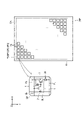
- FIG. 2 is a plan view showing an example of the pixel PX shown in FIG. 1.
- FIG. The sub-pixels SP1, SP2, and SP3 forming one pixel PX are each formed in a substantially rectangular shape extending in the second direction Y and arranged in the first direction X in the display area DA.
- the display elements 20 included in the sub-pixels SP1, SP2 and SP3 are connected to the pixel circuits 1 included in the sub-pixels SP1, SP2 and SP3 through the openings OP1.
- the opening OP1 is preferably formed so that the centers of the sub-pixels SP1, SP2, and SP3 are aligned with the center of the opening OP1. According to this, it is possible to provide light-emitting regions, which will be described in detail later, so as to extend from the centers of the sub-pixels SP1, SP2, and SP3.
- the size of the opening OP1 (area on the XY plane) is not limited to the illustrated size, and may be any size such as the same size as the display element 20, for example.
- the partition walls 30, which will be described in detail later, are formed in a lattice shape extending in the first direction X and the second direction Y in plan view, and surround the sub-pixels SP1, SP2, and SP3.
- the partition 30 may be called a rib.
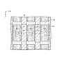
- FIG. 3 is a plan view showing another example of the pixel PX shown in FIG. 1.
- FIG. 3 differs from the example shown in FIG. 2 in that the partition walls 30 are formed in stripes.
- Each partition wall 30 extends in the second direction Y and is aligned in the first direction X.
- Each of the sub-pixels SP1, SP2, and SP3 is located between adjacent partition walls 30 . That is, in the first direction X, the sub-pixels and the partition walls are alternately arranged.
- the shape of the sub-pixels SP1, SP2, and SP3 is not limited to this. Any shape different from a rectangular shape, such as an arbitrary polygonal shape, a circular shape, an irregular shape, or the like, may be used. Also, the sub-pixels SP1, SP2, and SP3 may have different shapes.
- FIGS. 2 and 3 illustrate the case where the sub-pixels SP1, SP2, and SP3 are arranged in stripes, but the arrangement of the sub-pixels SP1, SP2, and SP3 is not limited to this.
- SP2 and SP3 may be arranged in a pentile manner, for example.
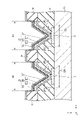
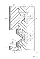
- FIG. 4 is a cross-sectional view showing an example of the display element 20 according to this embodiment.
- two display elements 20 adjacent in the first direction X are illustrated.
- the configurations of the two display elements 20 shown in FIG. 4 are the same except that the luminescent colors of the luminescent layers, which will be described later, are different.
- the pixel circuit 1 shown in FIG. 1 is arranged on a substrate 10 and covered with an insulating layer 11.
- the insulating layer 11 corresponds to a base layer of the display element 20, and is made of an insulating material such as polyimide, acrylic resin, silicon nitride (SiN), silicon oxide (SiO), or the like.
- the display element 20 includes a lower electrode E1, an organic layer OR, and an upper electrode E2.
- the lower electrode E1 is an electrode arranged for each sub-pixel or each display element, and is electrically connected to the drive transistor 3. Such a lower electrode E1 may be called a pixel electrode, a reflective electrode, an anode, or the like.
- the upper electrode E2 is an electrode arranged for each sub-pixel or each display element, and is electrically connected to each other across a plurality of adjacent sub-pixels or a plurality of display elements. Such an upper electrode E2 may be called a common electrode, a counter electrode, a cathode, or the like.
- the lower electrode E1 is arranged on the insulating layer 11 and connected to the driving transistor 3 through the opening OP1 formed in the insulating layer 11.
- the opening OP ⁇ b>1 is a through hole that is formed in a region overlapping the driving transistor 3 and penetrates the insulating layer 11 to the driving transistor 3 .
- the lower electrode E1 is a transparent electrode made of a transparent conductive material such as indium tin oxide (ITO) or indium zinc oxide (IZO).
- the lower electrode E1 may be a metal electrode made of a metal material such as silver (Ag), aluminum (Al), titanium (Ti), molybdenum (Mo), tungsten (W), or the like.
- the lower electrode E1 may be a laminate of a transparent electrode and a metal electrode.
- the lower electrode E1 may be configured as a laminate in which a transparent electrode, a metal electrode, and a transparent electrode are laminated in this order, or may be configured as a laminate of three or more layers.
- the partition wall 30 is provided on the insulating layer 11 so as to cover the peripheral portion (end portion) of the lower electrode E1. By covering the periphery of the lower electrode E1 with the partition wall 30, it is possible to prevent the lower electrode E1 and the upper electrode E2 from coming into contact with each other and causing a short circuit.
- the opening OP1 is positioned between two adjacent partition walls 30 .
- the organic layer OR is arranged on the lower electrode E1. That is, the organic layer OR is arranged in the opening OP1 and covers the lower electrode E1.
- Such an organic layer OR includes a first EL (Electro Luminescence) layer EL1 (first organic layer).
- the organic layer OR further includes a second EL layer EL2 (second organic layer). The first EL layer EL1 and the second EL layer EL2 are stacked in order from the lower electrode E1 side.
- the first EL layer EL1 includes a light-emitting layer that emits red, green, or blue light, and a functional layer.
- the functional layers included in the first EL layer EL1 are, for example, a hole injection layer, a hole transport layer, an electron blocking layer, etc., but may be other functional layers.
- the second EL layer EL2 includes functional layers.
- the functional layers included in the second EL layer EL2 are, for example, a hole blocking layer, an electron transport layer, an electron injection layer, etc., but may be other functional layers.
- Each of the illustrated first EL layer EL1 and second EL layer EL2 is not limited to a single layer, and may be a laminate in which a plurality of layers are laminated. In this case, the lower layer may be formed smaller, and the lower layer may be covered with an upper layer positioned above the lower layer. Also, part of the functional layers included in the first EL layer EL1 and the second EL layer EL2 may be omitted.
- the upper electrode E2 covers the organic layer OR and the partition wall 30.
- the upper electrode E2 is a common layer commonly used over the plurality of display elements 20.
- the upper electrode E2 is a transparent electrode made of, for example, a transparent conductive material such as ITO or IZO.
- the upper electrode E2 may be a semi-transparent metal electrode made of a metal material such as magnesium (Mg), silver (Ag), aluminum (Al), or the like.
- the upper electrode E2 is electrically connected to a power supply line arranged in the display area DA or a power supply line arranged outside the display area DA.
- the lower electrode E1 corresponds to the anode and the upper electrode E2 corresponds to the cathode.
- the upper electrode E2 corresponds to the anode and the lower electrode E1 corresponds to the cathode.
- the functional layers included in the first EL layer EL1 include at least one of a hole injection layer, a hole transport layer, and an electron blocking layer
- the functional layers included in the second EL layer EL2 include a hole blocking layer. At least one of a layer, an electron-transporting layer, and an electron-injecting layer.
- the organic layer OR arranged between the lower electrode E1 arranged in the opening OP1 and the upper electrode E2 arranged as a common layer is located in the portion of the display element 20.
- a light emitting region can be formed. That is, the light emitting region of the display element 20 can be formed in the region R1 including the lower surface UN1 of the opening OP1, the slopes S1 and S2 of the opening OP1, and part of the upper surfaces UP1 and UP2 of the insulating layer 11. .
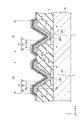
- the organic layer OR is not arranged in the opening OP1 for connecting the lower electrode E1 and the driving transistor 3, but the partition wall 30 is arranged.
- the display element 20 differs from the display element 20 according to the present embodiment in that the organic layer OR is arranged in the opening OP2 positioned between the two partitions 30 .
- the organic layer OR is arranged through the opening OP2 and connected to the lower electrode E1 exposed in the opening OP2. Therefore, in the display element 20A in the comparative example, the light emitting region is formed in the region RA including the lower surface UN1A of the opening OP2, the slopes S1A and S2A of the opening OP2, and part of the upper surfaces UP1A and UP2A of the partition wall 30. It is formed.
- the partition 30 intervenes between the lower electrode E1 and the upper electrode E2 at the slopes S1A and S2A of the opening OP2 and part of the upper surfaces UP1A and UP2A of the partition 30, the organic layer OR Of these, there is a problem that the portions arranged on the slopes S1A and S2A of the opening OP2 and parts of the upper surfaces UP1A and UP2A of the partition 30 hardly emit light.
- the portion where layers other than the organic layer OR are interposed between the lower electrode E1 and the upper electrode E2 is the light emitting region. Since it is not in the region R1, it is possible to cause the organic layer OR to emit light over the entire light emitting region.
- the number of the openings OP1 for connecting the lower electrode E1 and the driving transistor 3 increases as the definition progresses.
- the area of the opening OP2 located between the two adjacent partition walls 30 becomes narrower, and the light emitting area of the display element 20A may decrease. According to this, since the luminance is lowered, the display image becomes dark, and the display quality of the display device is deteriorated.
- the entire surface of the opening OP1 for connecting the lower electrode E1 and the driving transistor 3 can be used as a light emitting region. Even if the definition of the device DSP increases and the number of openings OP1 increases, the light emitting area of the display element 20 does not decrease, and it is possible to suppress the decrease in luminance accompanying the above-described increase in definition. It is possible to suppress deterioration in display quality.
- the display device DSP includes a plurality of sub-pixels SP (pixels PX ). According to this, even if the definition of the display device DSP progresses, the light emitting area of the light emitting element 20 does not decrease, and a sufficient light emitting area can be secured. Therefore, it is possible to suppress deterioration of display quality.
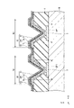
- the display device DSP according to the second embodiment differs from the above-described first embodiment in that the partition wall 30 for partitioning the organic layer OR included in the display element 20 is not provided.
- the description of the configuration common to the above first embodiment will be omitted, and mainly the differences from the above first embodiment will be described.
- FIG. 6 is a cross-sectional view showing an example of the display element 20 according to this embodiment.
- two display elements 20 adjacent in the first direction X are illustrated.
- the configurations of the two display elements 20 shown in FIG. 6 are the same except that the luminescent colors of the luminescent layers are different.
- only the driving transistor 3 included in the pixel circuit 1 is illustrated in a simplified manner.
- the driving transistor 3 is arranged on the base material 10 and covered with the insulating layer 11 .
- a lower electrode E1 forming the display element 20 is connected to the driving transistor 3 through an opening OP1 formed in the insulating layer 11 .
- the peripheral portion of the lower electrode E1 has a forward tapered shape.
- the organic layer OR forming the display element 20 is arranged in the opening OP1 and covers the lower electrode E1.
- the organic layer OR includes a first EL layer EL1 including a light-emitting layer and a functional layer and a second EL layer EL2 including a functional layer, as in the first embodiment described above. Note that, as shown in FIG. 6, both the peripheral edge portion of the first EL layer EL1 and the peripheral edge portion of the second EL layer EL2 have a forward tapered shape, unlike the above-described first embodiment.
- FIG. 6 shows the case where the peripheral edge of the lower electrode E1 and the peripheral edge of the first EL layer EL1 are aligned on the same oblique line, but the peripheral edge of the lower electrode E1 and the peripheral edge of the first EL layer EL1 1 and 2 are not necessarily arranged on the same oblique line, and the peripheral edge of the first EL layer EL1 may partially cover the peripheral edge of the lower electrode E1.
- the upper electrode E2 covers the organic layer OR.
- the organic layer OR arranged between the lower electrode E1 arranged in the opening OP1 and the upper electrode E2 arranged as a common layer is located in the portion of the display element 20.
- a light emitting region can be formed. That is, the light emitting region of the display element 20 can be formed in the region R2 including the lower surface UN11 of the opening OP1, the slopes S11 and S12 of the opening OP1, and part of the upper surfaces UP11 and UP12 of the insulating layer 11. .
- the display element 20 having the configuration shown in FIG. 6 can be formed, for example, by the forming steps shown in FIGS. 7A to 7D.
- 7A to 7D are diagrams for explaining the steps of forming the cross-sectional structure shown in FIG.
- the drive transistor 3 (pixel circuit 1) is provided on the base material 10 .
- an insulating layer 11 is formed so as to cover the driving transistor 3 provided on the base material 10 .
- An opening OP ⁇ b>1 is formed in a region of the insulating layer 11 that overlaps with the driving transistor 3 . As a result, the surface of the driving transistor 3 is exposed from the insulating layer 11 .
- an inversely tapered mask PM is formed. be provided.
- the lower surface UN11 of the opening OP1 on the left side of the figure where the display element 20 of the first color is arranged, the slopes S11 and S12 of the opening OP1, the upper surface UP11 of the insulating layer 11 and A reverse tapered mask PM is provided in a region other than a part of the UP 12 .
- a layer structure other than the common layer included in the display element 20 of the first color is formed.
- the lower electrode E1, the first EL layer EL1, and the second EL layer EL2 are formed in this order.
- the lower surface UN11 of the opening OP1 on the left side of the drawing where the display element 20 of the first color is arranged, the slopes S11 and S12 of the opening OP1, and the upper surfaces UP11 and UP12 of the insulating layer 11 are partly formed.
- the mask PM having an inverse tapered shape is provided in the regions other than and, the peripheral edge portion of the lower electrode E1 formed in the opening portion OP1, the peripheral edge portion of the first EL layer EL1, and the peripheral edge portion of the second EL layer EL2. Each part is formed in a forward tapered shape.
- the second EL layer EL2 is formed over a wider range than the lower electrode E1 and the first EL layer EL1. According to this, as shown in FIG. 7B, the peripheral edge portion of the lower electrode E1 formed in the opening OP1 and the peripheral edge portion of the first EL layer EL1 can be covered with the second EL layer EL2.
- the mask PM is removed.
- the lower electrode E1 the first EL layer EL1 including the light emitting layer of the first color
- the second EL layer EL2 are arranged only in the opening OP1 on the left side of the drawing. More specifically, the lower electrode E1 and the first color are formed in portions overlapping the lower surface UN11 of the opening OP1 on the left side of the drawing, the slopes S11 and S12 of the opening OP1, and the upper surfaces UP11 and UP12 of the insulating layer 11.
- a first EL layer EL1 and a second EL layer EL2 each including a light emitting layer are arranged.
- a reverse tapered mask PM is provided in a region other than the region where the display element 20 is arranged.
- the lower surface UN11 of the opening OP1 on the right side of the figure where the display element 20 of the second color is arranged, the slopes S11 and S12 of the opening OP, the upper surface UP12 of the insulating layer 11 and the A reverse tapered mask PM is provided in a region other than a part of the UP 13 .
- the layer structure other than the common layer included in the display element 20 of the second color is formed.
- the lower electrode E1, the first EL layer EL1, and the second EL layer EL2 are sequentially formed in the opening OP1 on the right side of the figure.
- the mask PM is removed.
- the lower electrode E1 the first EL layer EL1 including the light emitting layer of the second color
- the second EL layer EL2 are arranged in the opening OP1 on the right side of the drawing. More specifically, the lower electrode E1 and the second color are applied to portions overlapping the lower surface UN11 of the opening OP1 on the right side of the drawing, the slopes S11 and S12 of the opening OP1, and the upper surfaces UP12 and UP13 of the insulating layer 11.
- a first EL layer EL1 and a second EL layer EL2 each including a light emitting layer are arranged.
- FIGS. 7A to 7D the formation steps shown in FIGS. 7A to 7D described above are repeated for the display elements 20 of colors different from the first color and the second color.
- a layer structure other than the common layer included in the display element 20 that is, the lower electrode E1, the first EL layer EL1, and the second EL layer EL2 is formed in all the openings OP1 formed in the insulating layer 11. .
- an upper electrode E2 included as a common layer in the display element 20 is formed over the entire surface of the insulating layer 11 so as to cover the insulating layer 11 and the second EL layer EL2 (organic layer OR). Thereby, the display element 20 having the cross-sectional structure shown in FIG. 6 is formed.
- a reverse tapered mask PM is used to form a lower electrode E1, a first EL layer EL1 and a second EL layer EL2, which are layers other than the common layer included in the display element 20. is formed, as described above, the peripheral edge portion of the lower electrode E1, the peripheral edge portion of the first EL layer EL1, and the peripheral edge portion of the second EL layer EL2 can each be formed into a forward tapered shape.
- the peripheral edges of the lower electrode E1, the first EL layer EL1 and the second EL layer EL2 are all formed substantially vertically. Therefore, when the upper electrode E2 is formed on the second EL layer EL2, the upper electrode E2 may be cut off.
- the peripheral portions of the lower electrode E1, the first EL layer EL1, and the second EL layer EL2 can be formed into a forward tapered shape. Therefore, it is possible to reduce the risk of disconnection that may occur when the upper electrode E2 is formed on the second EL layer EL2.
- the peripheral edge portion of the lower electrode E1, the peripheral edge portion of the first EL layer EL1, and the first EL layer EL1 are formed.
- the periphery of the second EL layer EL2 can be formed in a forward tapered shape, and the second EL layer EL2 can cover at least the periphery of the lower electrode E1 without discontinuity. This eliminates the need to provide the partition wall 30 for preventing contact between the lower electrode E1 and the upper electrode E2. In other words, the step of providing the partitions 30 can be omitted, and the manufacturing cost can be reduced by the amount of the partitions 30 that can be omitted.
- the display element 20 has the lower electrode E1, the first EL layer EL1, and the second EL layer EL2, which are arranged on the upper surface UP of the insulating layer 11, to the extent that the partition 30 is not provided. , can extend in the direction of the adjacent display element 20 . That is, it is possible to expand the light emitting area of the display element 20 as compared with the first embodiment described above.
- the second embodiment described above it is possible not only to obtain the same effects as those of the first embodiment, but also to omit the step of providing the partition wall 30, reduce the manufacturing cost, and increase the light emitting area of the display element 20. It is possible to achieve expansion.
- FIG. 8 is a cross-sectional view showing an example of the display element 20 according to the first modified example of this embodiment.
- two display elements 20 adjacent in the first direction X are illustrated.
- the two display elements 20 shown in FIG. 8 have the same configuration except that the emission colors of the light-emitting layers are different.
- only the driving transistor 3 included in the pixel circuit 1 is illustrated in a simplified manner.
- the second EL layer EL2 included in the organic layer OR is used over a plurality of display elements 20 instead of being provided for each display element 20. It is different from the configuration shown in FIG. 6 in that it is provided as a common layer that
- the peripheral edge portion of the lower electrode E1 and the peripheral edge portion of the first EL layer EL1 can be formed in a forward tapered shape by using the reverse tapered mask PM. Therefore, at least the peripheral portion of the lower electrode E1 can be covered with the second EL layer EL2 without discontinuity. That is, since it is possible to omit the partition wall 30 for preventing the lower electrode E1 and the upper electrode E2 from coming into contact with each other, the configuration according to this modification is similar to that of the above-described second embodiment. effect can be obtained.
- FIG. 9 is a cross-sectional view showing an example of the display element 20 according to the second modified example of this embodiment.
- two display elements 20 adjacent in the first direction X are illustrated.
- the configurations of the two display elements 20 shown in FIG. 9 are the same except that the luminescent colors of the luminescent layers are different.
- only the drive transistor 3 included in the pixel circuit 1 is illustrated in a simplified manner.
- the display element 20 covers the peripheral edge of the lower electrode E1 and the peripheral edge of the first EL layer EL1 included in the organic layer OR.
- the configuration differs from that shown in FIG. 6 in that it further includes an insulating film 12 covered with the second EL layer EL2.
- the insulating film 12 may be provided so as to cover at least the peripheral portion of the lower electrode E1.
- the insulating film 12 is made of an insulating material such as silicon nitride (SiN), and is provided to prevent the lower electrode E1 and the upper electrode E2 from coming into contact with each other and short-circuiting.
- SiN silicon nitride
- the insulating film 12 only needs to be provided in a smaller area than the partition 30.
- the insulating film 12 according to this modification may be mounted by replacing it with a carrier block layer such as a hole block layer or an electron block layer.
- the light-emitting element 20 having the light-emitting region of the opening OP1 for connecting the lower electrode E1 and the driving transistor 3, thereby preventing deterioration in display quality. It is possible to provide a display device DSP that can be suppressed.
Abstract
Description
基材と、前記基材の上に配置された複数の画素回路と、前記基材および前記各画素回路を覆う絶縁層と、前記絶縁層において前記各画素回路と重なる位置に各々形成される複数の開口部と、前記各画素回路により各々駆動制御される複数の表示素子と、前記絶縁層の上に配置され、前記各表示素子を区画する隔壁と、を備え、前記各表示素子は、前記絶縁層の上に配置され、前記開口部を通って前記画素回路に接続される下部電極と、前記開口部に配置され、前記下部電極を覆う有機層と、前記有機層を覆う上部電極と、を各々備え、前記下部電極と前記有機層とは、前記開口部の全面に亘って接し、前記有機層と前記上部電極とは、前記開口部の全面に亘って接し、前記下部電極の周縁部は、前記隔壁により覆われている。 A display device according to one embodiment includes:
a substrate, a plurality of pixel circuits disposed on the substrate, an insulating layer covering the substrate and the pixel circuits, and a plurality of insulating layers formed at positions overlapping the pixel circuits. , a plurality of display elements driven and controlled by the respective pixel circuits, and partition walls arranged on the insulating layer and partitioning the display elements, wherein the display elements each comprise the a lower electrode disposed on an insulating layer and connected to the pixel circuit through the opening, an organic layer disposed in the opening and covering the lower electrode, and an upper electrode covering the organic layer; wherein the lower electrode and the organic layer are in contact with each other over the entire surface of the opening, the organic layer and the upper electrode are in contact with each other over the entire surface of the opening, and a peripheral edge portion of the lower electrode are covered by the partition.
基材と、前記基材の上に配置された複数の画素回路と、前記基材および前記各画素回路を覆う絶縁層と、前記絶縁層において前記各画素回路と重なる位置に各々形成される複数の開口部と、前記各画素回路により各々駆動制御される複数の表示素子と、を備え、前記各表示素子は、前記絶縁層の上に配置され、前記開口部を通って前記画素回路に接続される下部電極と、前記開口部に配置され、前記下部電極を覆う有機層と、前記有機層を覆う上部電極と、を各々備え、前記下部電極と前記有機層とは、前記開口部の全面に亘って接し、前記有機層と前記上部電極とは、前記開口部の全面に亘って接している。 A display device according to one embodiment includes:
a substrate, a plurality of pixel circuits disposed on the substrate, an insulating layer covering the substrate and the pixel circuits, and a plurality of insulating layers formed at positions overlapping the pixel circuits. and a plurality of display elements driven and controlled by the respective pixel circuits, the display elements being arranged on the insulating layer and connected to the pixel circuits through the openings. an organic layer disposed in the opening to cover the lower electrode; and an upper electrode covering the organic layer, wherein the lower electrode and the organic layer cover the entire surface of the opening. The organic layer and the upper electrode are in contact with each other over the entire surface of the opening.
なお、開示はあくまで一例に過ぎず、当業者において、発明の主旨を保っての適宜変更について容易に想到し得るものについては、当然に本発明の範囲に含有されるものである。また、図面は、説明をより明確にするため、実施の態様に比べて模式的に表される場合があるが、あくまで一例であって、本発明の解釈を限定するものではない。また、本明細書と各図において、既出の図に関して前述したものと同一または類似した機能を発揮する構成要素には同一の参照符号を付し、重複する詳細な説明を省略することがある。 Some embodiments will be described with reference to the drawings.
It should be noted that the disclosure is merely an example, and those skilled in the art will naturally include within the scope of the present invention any suitable modifications that can be easily conceived while maintaining the gist of the invention. Also, in order to make the description clearer, the drawings may be represented schematically compared to the embodiments, but they are only examples and do not limit the interpretation of the present invention. In addition, in this specification and each figure, the same reference numerals are given to constituent elements that perform the same or similar functions as those described above with respect to the previous figures, and redundant detailed description may be omitted.
図1は、本実施形態に係る表示装置DSPの一構成例を示す図である。表示装置DSPは、絶縁性の基材10の上に、画像を表示する表示部DAを備えている。基材10は、ガラスであってもよいし、可撓性を有する樹脂フィルムであってもよい。 (First embodiment)
FIG. 1 is a diagram showing a configuration example of a display device DSP according to this embodiment. The display device DSP includes a display section DA for displaying an image on an
副画素SPは、画素回路1と、画素回路1によって駆動制御される表示素子20と、を備えている。画素回路1は、画素スイッチ2と、駆動トランジスタ3と、キャパシタ4と、を備えている。画素スイッチ2および駆動トランジスタ3は、例えば薄膜トランジスタ(TFT)により構成されたスイッチ素子である。 A configuration example of one sub-pixel SP included in the pixel PX will be briefly described.
The sub-pixel SP includes a
1個の画素PXを構成する副画素SP1、SP2、SP3は、表示部DAにおいて、それぞれ第2方向Yに延びた略長方形状に形成され、第1方向Xに並んでいる。 FIG. 2 is a plan view showing an example of the pixel PX shown in FIG. 1. FIG.
The sub-pixels SP1, SP2, and SP3 forming one pixel PX are each formed in a substantially rectangular shape extending in the second direction Y and arranged in the first direction X in the display area DA.
図3に示す例は、図2に示した例と比較して、隔壁30がストライプ状に形成された点で相違している。隔壁30の各々は、第2方向Yに延出し、第1方向Xに並んでいる。副画素SP1、SP2、SP3の各々は、隣接する隔壁30の間に位置している。つまり、第1方向Xにおいて、副画素と隔壁とが交互に並んでいる。 FIG. 3 is a plan view showing another example of the pixel PX shown in FIG. 1. FIG.
The example shown in FIG. 3 differs from the example shown in FIG. 2 in that the
次に、第2実施形態について説明する。第2実施形態に係る表示装置DSPは、表示素子20に含まれる有機層ORを区画するための隔壁30が設けられない点で、上記した第1実施形態と相違している。なお、本実施形態においては、上記した第1実施形態と共通する構成についての説明は省略し、主に、上記した第1実施形態と相違する点について説明する。 (Second embodiment)
Next, a second embodiment will be described. The display device DSP according to the second embodiment differs from the above-described first embodiment in that the
(第1変形例)
図8は、本実施形態の第1変形例に係る表示素子20の一例を示す断面図である。図8では、第1方向Xに隣接する2つの表示素子20を図示している。なお、図8に示す2つの表示素子20の構成は、発光層の発光色が異なること以外は同様である。また、図8では、画素回路1に含まれる駆動トランジスタ3のみを簡略化して図示している。 Modifications of this embodiment will be described below.
(First modification)
FIG. 8 is a cross-sectional view showing an example of the
図9は、本実施形態の第2変形例に係る表示素子20の一例を示す断面図である。図9では、第1方向Xに隣接する2つの表示素子20を図示している。なお、図9に示す2つの表示素子20の構成は、発光層の発光色が異なること以外は同様である。また、図9では、画素回路1に含まれる駆動トランジスタ3のみを簡略化して図示している。 (Second modification)
FIG. 9 is a cross-sectional view showing an example of the
Claims (12)
- 基材と、
前記基材の上に配置された複数の画素回路と、
前記基材および前記各画素回路を覆う絶縁層と、
前記絶縁層において前記各画素回路と重なる位置に各々形成される複数の開口部と、
前記各画素回路により各々駆動制御される複数の表示素子と、
前記絶縁層の上に配置され、前記各表示素子を区画する隔壁と、を備え、
前記各表示素子は、
前記絶縁層の上に配置され、前記開口部を通って前記画素回路に接続される下部電極と、
前記開口部に配置され、前記下部電極を覆う有機層と、
前記有機層を覆う上部電極と、を各々備え、
前記下部電極と前記有機層とは、前記開口部の全面に亘って接し、
前記有機層と前記上部電極とは、前記開口部の全面に亘って接し、
前記下部電極の周縁部は、前記隔壁により覆われている、
表示装置。 a substrate;
a plurality of pixel circuits disposed on the substrate;
an insulating layer covering the base material and each pixel circuit;
a plurality of openings respectively formed in the insulating layer at positions overlapping with the pixel circuits;
a plurality of display elements driven and controlled by the respective pixel circuits;
a partition disposed on the insulating layer and partitioning the display elements;
Each display element is
a lower electrode disposed on the insulating layer and connected to the pixel circuit through the opening;
an organic layer disposed in the opening and covering the lower electrode;
and an upper electrode covering the organic layer,
the lower electrode and the organic layer are in contact with each other over the entire surface of the opening;
the organic layer and the upper electrode are in contact with each other over the entire surface of the opening;
a peripheral edge of the lower electrode is covered with the partition wall;
display device. - 前記隔壁は、平面視において、格子状に形成されている、
請求項1に記載の表示装置。 The partition walls are formed in a lattice shape in plan view,
The display device according to claim 1. - 前記隔壁は、平面視において、ストライプ状に形成されている、
請求項1に記載の表示装置。 The partition wall is formed in a stripe shape in plan view,
The display device according to claim 1. - 基材と、
前記基材の上に配置された複数の画素回路と、
前記基材および前記各画素回路を覆う絶縁層と、
前記絶縁層において前記各画素回路と重なる位置に各々形成される複数の開口部と、
前記各画素回路により各々駆動制御される複数の表示素子と、を備え、
前記各表示素子は、
前記絶縁層の上に配置され、前記開口部を通って前記画素回路に接続される下部電極と、
前記開口部に配置され、前記下部電極を覆う有機層と、
前記有機層を覆う上部電極と、を各々備え、
前記下部電極と前記有機層とは、前記開口部の全面に亘って接し、
前記有機層と前記上部電極とは、前記開口部の全面に亘って接している、
表示装置。 a substrate;
a plurality of pixel circuits disposed on the substrate;
an insulating layer covering the base material and each pixel circuit;
a plurality of openings respectively formed in the insulating layer at positions overlapping with the pixel circuits;
a plurality of display elements each driven and controlled by each pixel circuit;
Each display element is
a lower electrode disposed on the insulating layer and connected to the pixel circuit through the opening;
an organic layer disposed in the opening and covering the lower electrode;
and an upper electrode covering the organic layer,
the lower electrode and the organic layer are in contact with each other over the entire surface of the opening;
wherein the organic layer and the upper electrode are in contact with each other over the entire surface of the opening;
display device. - 前記下部電極の周縁部は、前記有機層により覆われており、前記下部電極と前記上部電極とは接していない、
請求項4に記載の表示装置。 a peripheral portion of the lower electrode is covered with the organic layer, and the lower electrode and the upper electrode are not in contact;
The display device according to claim 4. - 前記有機層は、少なくとも第1有機層と、少なくとも1つの機能層を含む第2有機層と、を含み、
前記下部電極の周縁部、前記第1有機層の周縁部および前記第2有機層の周縁部はいずれも、順テーパー形状である、
請求項5に記載の表示装置。 The organic layers include at least a first organic layer and a second organic layer including at least one functional layer,
A peripheral edge portion of the lower electrode, a peripheral edge portion of the first organic layer, and a peripheral edge portion of the second organic layer are all forward tapered,
The display device according to claim 5. - 前記下部電極の周縁部は、少なくとも前記第2有機層の周縁部により覆われている、
請求項6に記載の表示装置。 a peripheral edge of the lower electrode is covered with at least a peripheral edge of the second organic layer;
The display device according to claim 6. - 前記上部電極は、前記複数の表示素子に亘って配置されている、
請求項7に記載の表示装置。 The upper electrode is arranged over the plurality of display elements,
The display device according to claim 7. - 前記第2有機層は、前記複数の表示素子に亘って配置されている、
請求項8に記載の表示装置。 The second organic layer is arranged over the plurality of display elements,
The display device according to claim 8. - 前記下部電極の周縁部を覆い、前記有機層により覆われる絶縁膜をさらに備え、
前記下部電極と前記上部電極とは接していない、
請求項4に記載の表示装置。 further comprising an insulating film covering a peripheral portion of the lower electrode and covered with the organic layer;
the lower electrode and the upper electrode are not in contact;
The display device according to claim 4. - 前記下部電極の周縁部を覆い、前記有機層により覆われるキャリアブロック層をさらに備え、
前記下部電極と前記上部電極とは接していない、
請求項4に記載の表示装置。 further comprising a carrier block layer covering a peripheral portion of the lower electrode and covered with the organic layer;
the lower electrode and the upper electrode are not in contact;
The display device according to claim 4. - 前記キャリアブロック層は、正孔ブロック層および電子ブロック層の少なくとも1つを含む、
請求項11に記載の表示装置。 the carrier blocking layer comprises at least one of a hole blocking layer and an electron blocking layer;
The display device according to claim 11.
Priority Applications (3)
| Application Number | Priority Date | Filing Date | Title |
|---|---|---|---|
| CN202280014382.6A CN116868694A (en) | 2021-02-18 | 2022-02-09 | Display device |
| JP2023500774A JPWO2022176736A1 (en) | 2021-02-18 | 2022-02-09 | |
| US18/450,417 US20230389360A1 (en) | 2021-02-18 | 2023-08-16 | Display device |
Applications Claiming Priority (2)
| Application Number | Priority Date | Filing Date | Title |
|---|---|---|---|
| JP2021-024456 | 2021-02-18 | ||
| JP2021024456 | 2021-02-18 |
Related Child Applications (1)
| Application Number | Title | Priority Date | Filing Date |
|---|---|---|---|
| US18/450,417 Continuation US20230389360A1 (en) | 2021-02-18 | 2023-08-16 | Display device |
Publications (1)
| Publication Number | Publication Date |
|---|---|
| WO2022176736A1 true WO2022176736A1 (en) | 2022-08-25 |
Family
ID=82931642
Family Applications (1)
| Application Number | Title | Priority Date | Filing Date |
|---|---|---|---|
| PCT/JP2022/005126 WO2022176736A1 (en) | 2021-02-18 | 2022-02-09 | Display device |
Country Status (4)
| Country | Link |
|---|---|
| US (1) | US20230389360A1 (en) |
| JP (1) | JPWO2022176736A1 (en) |
| CN (1) | CN116868694A (en) |
| WO (1) | WO2022176736A1 (en) |
Citations (7)
| Publication number | Priority date | Publication date | Assignee | Title |
|---|---|---|---|---|
| JP2003022035A (en) * | 2001-07-10 | 2003-01-24 | Sharp Corp | Organic el panel and its manufacturing method |
| JP2003091246A (en) * | 2001-09-18 | 2003-03-28 | Matsushita Electric Ind Co Ltd | Organic electro-luminescence display panel and manufacturing method therefor |
| JP2010245059A (en) * | 2010-08-05 | 2010-10-28 | Fujifilm Corp | Organic electroluminescent device, device for manufacturing the same, and display device |
| WO2011138817A1 (en) * | 2010-05-07 | 2011-11-10 | パナソニック株式会社 | Organic el display panel and method for producing same |
| WO2012017494A1 (en) * | 2010-08-06 | 2012-02-09 | パナソニック株式会社 | Organic el display panel, display device, and method for manufacturing organic el display panel |
| WO2016167354A1 (en) * | 2015-04-16 | 2016-10-20 | シャープ株式会社 | Organic electroluminescence device |
| WO2021261493A1 (en) * | 2020-06-23 | 2021-12-30 | 三国電子有限会社 | Reversed-structure electroluminescence element having coated inorganic transparent oxide semiconductor electron transport layer |
-
2022
- 2022-02-09 WO PCT/JP2022/005126 patent/WO2022176736A1/en active Application Filing
- 2022-02-09 JP JP2023500774A patent/JPWO2022176736A1/ja active Pending
- 2022-02-09 CN CN202280014382.6A patent/CN116868694A/en active Pending
-
2023
- 2023-08-16 US US18/450,417 patent/US20230389360A1/en active Pending
Patent Citations (7)
| Publication number | Priority date | Publication date | Assignee | Title |
|---|---|---|---|---|
| JP2003022035A (en) * | 2001-07-10 | 2003-01-24 | Sharp Corp | Organic el panel and its manufacturing method |
| JP2003091246A (en) * | 2001-09-18 | 2003-03-28 | Matsushita Electric Ind Co Ltd | Organic electro-luminescence display panel and manufacturing method therefor |
| WO2011138817A1 (en) * | 2010-05-07 | 2011-11-10 | パナソニック株式会社 | Organic el display panel and method for producing same |
| JP2010245059A (en) * | 2010-08-05 | 2010-10-28 | Fujifilm Corp | Organic electroluminescent device, device for manufacturing the same, and display device |
| WO2012017494A1 (en) * | 2010-08-06 | 2012-02-09 | パナソニック株式会社 | Organic el display panel, display device, and method for manufacturing organic el display panel |
| WO2016167354A1 (en) * | 2015-04-16 | 2016-10-20 | シャープ株式会社 | Organic electroluminescence device |
| WO2021261493A1 (en) * | 2020-06-23 | 2021-12-30 | 三国電子有限会社 | Reversed-structure electroluminescence element having coated inorganic transparent oxide semiconductor electron transport layer |
Also Published As
| Publication number | Publication date |
|---|---|
| US20230389360A1 (en) | 2023-11-30 |
| JPWO2022176736A1 (en) | 2022-08-25 |
| CN116868694A (en) | 2023-10-10 |
Similar Documents
| Publication | Publication Date | Title |
|---|---|---|
| CN108155210B (en) | Organic light emitting display device | |
| JP2018073821A (en) | Flat display device connecting front and rear of substrate via through hole | |
| US20170250362A1 (en) | Display device | |
| WO2016132954A1 (en) | Electroluminescence device | |
| CN114551519A (en) | Display device | |
| WO2022163123A1 (en) | Display device | |
| CN114765208A (en) | Display device | |
| US20230422551A1 (en) | Display device | |
| KR20180077856A (en) | Electroluminescent Display Device | |
| US20220416209A1 (en) | Display device and manufacturing method of the same | |
| WO2022176736A1 (en) | Display device | |
| JP2022154588A (en) | Display device | |
| WO2015119086A1 (en) | Electroluminescent device | |
| WO2022191112A1 (en) | Display device | |
| WO2014174804A1 (en) | Method for producing el display device | |
| KR20150024495A (en) | Organic light emitting diode display device | |
| JP2020027883A (en) | Organic el display and method for manufacturing organic el display | |
| WO2022172670A1 (en) | Display device | |
| WO2022168513A1 (en) | Display device and method for manufacturing display device | |
| US20240074231A1 (en) | Display device and manufacturing method of display device | |
| WO2022176395A1 (en) | Display device | |
| WO2022181038A1 (en) | Display device | |
| JP2022160194A (en) | Display device | |
| JP2018181897A (en) | Organic electroluminescent display device | |
| KR20130065222A (en) | Organic light emitting diode device |
Legal Events
| Date | Code | Title | Description |
|---|---|---|---|
| 121 | Ep: the epo has been informed by wipo that ep was designated in this application |
Ref document number: 22756057 Country of ref document: EP Kind code of ref document: A1 |
|
| ENP | Entry into the national phase |
Ref document number: 2023500774 Country of ref document: JP Kind code of ref document: A |
|
| WWE | Wipo information: entry into national phase |
Ref document number: 202280014382.6 Country of ref document: CN |
|
| NENP | Non-entry into the national phase |
Ref country code: DE |
|
| 122 | Ep: pct application non-entry in european phase |
Ref document number: 22756057 Country of ref document: EP Kind code of ref document: A1 |