WO2021261493A1 - Reversed-structure electroluminescence element having coated inorganic transparent oxide semiconductor electron transport layer - Google Patents
Reversed-structure electroluminescence element having coated inorganic transparent oxide semiconductor electron transport layer Download PDFInfo
- Publication number
- WO2021261493A1 WO2021261493A1 PCT/JP2021/023638 JP2021023638W WO2021261493A1 WO 2021261493 A1 WO2021261493 A1 WO 2021261493A1 JP 2021023638 W JP2021023638 W JP 2021023638W WO 2021261493 A1 WO2021261493 A1 WO 2021261493A1
- Authority
- WO
- WIPO (PCT)
- Prior art keywords
- electrode
- electron transport
- layer
- transport layer
- insulating layer
- Prior art date
Links
- 238000005401 electroluminescence Methods 0.000 title claims abstract description 45
- 239000004065 semiconductor Substances 0.000 title claims description 139
- 239000000463 material Substances 0.000 claims abstract description 227
- 229910044991 metal oxide Inorganic materials 0.000 claims abstract description 72
- 150000004706 metal oxides Chemical class 0.000 claims abstract description 71
- 239000000758 substrate Substances 0.000 claims abstract description 37
- 238000004519 manufacturing process Methods 0.000 claims abstract description 24
- 239000000203 mixture Substances 0.000 claims abstract description 24
- 239000007788 liquid Substances 0.000 claims abstract description 22
- 239000002904 solvent Substances 0.000 claims abstract description 22
- XLOMVQKBTHCTTD-UHFFFAOYSA-N Zinc monoxide Chemical compound [Zn]=O XLOMVQKBTHCTTD-UHFFFAOYSA-N 0.000 claims description 51
- 229910052751 metal Inorganic materials 0.000 claims description 48
- 239000002184 metal Substances 0.000 claims description 46
- 238000000034 method Methods 0.000 claims description 46
- 239000011787 zinc oxide Substances 0.000 claims description 37
- VYPSYNLAJGMNEJ-UHFFFAOYSA-N Silicium dioxide Chemical compound O=[Si]=O VYPSYNLAJGMNEJ-UHFFFAOYSA-N 0.000 claims description 11
- 229910052814 silicon oxide Inorganic materials 0.000 claims description 10
- TWNQGVIAIRXVLR-UHFFFAOYSA-N oxo(oxoalumanyloxy)alumane Chemical compound O=[Al]O[Al]=O TWNQGVIAIRXVLR-UHFFFAOYSA-N 0.000 claims description 8
- XOLBLPGZBRYERU-UHFFFAOYSA-N tin dioxide Chemical compound O=[Sn]=O XOLBLPGZBRYERU-UHFFFAOYSA-N 0.000 claims description 8
- 229910001887 tin oxide Inorganic materials 0.000 claims description 8
- 150000001408 amides Chemical class 0.000 claims description 7
- AJNVQOSZGJRYEI-UHFFFAOYSA-N digallium;oxygen(2-) Chemical compound [O-2].[O-2].[O-2].[Ga+3].[Ga+3] AJNVQOSZGJRYEI-UHFFFAOYSA-N 0.000 claims description 7
- 229910001195 gallium oxide Inorganic materials 0.000 claims description 7
- 239000000395 magnesium oxide Substances 0.000 claims description 6
- CPLXHLVBOLITMK-UHFFFAOYSA-N magnesium oxide Inorganic materials [Mg]=O CPLXHLVBOLITMK-UHFFFAOYSA-N 0.000 claims description 6
- 229910003437 indium oxide Inorganic materials 0.000 claims description 5
- PJXISJQVUVHSOJ-UHFFFAOYSA-N indium(iii) oxide Chemical compound [O-2].[O-2].[O-2].[In+3].[In+3] PJXISJQVUVHSOJ-UHFFFAOYSA-N 0.000 claims description 5
- 150000003839 salts Chemical class 0.000 claims description 5
- QGLKJKCYBOYXKC-UHFFFAOYSA-N nonaoxidotritungsten Chemical compound O=[W]1(=O)O[W](=O)(=O)O[W](=O)(=O)O1 QGLKJKCYBOYXKC-UHFFFAOYSA-N 0.000 claims description 4
- 229910001930 tungsten oxide Inorganic materials 0.000 claims description 4
- AXZKOIWUVFPNLO-UHFFFAOYSA-N magnesium;oxygen(2-) Chemical compound [O-2].[Mg+2] AXZKOIWUVFPNLO-UHFFFAOYSA-N 0.000 claims description 3
- 238000004020 luminiscence type Methods 0.000 claims 1
- 238000001579 optical reflectometry Methods 0.000 claims 1
- 238000000576 coating method Methods 0.000 abstract description 21
- 239000011248 coating agent Substances 0.000 abstract description 8
- 239000010410 layer Substances 0.000 description 914
- 230000032258 transport Effects 0.000 description 364
- 239000010408 film Substances 0.000 description 164
- 238000002347 injection Methods 0.000 description 103
- 239000007924 injection Substances 0.000 description 103
- 239000000969 carrier Substances 0.000 description 39
- 229910006404 SnO 2 Inorganic materials 0.000 description 31
- 230000006870 function Effects 0.000 description 27
- 230000005684 electric field Effects 0.000 description 24
- 230000005525 hole transport Effects 0.000 description 24
- 238000004544 sputter deposition Methods 0.000 description 21
- -1 ZnO metal oxide Chemical class 0.000 description 20
- 229910005191 Ga 2 O 3 Inorganic materials 0.000 description 18
- 229910052718 tin Inorganic materials 0.000 description 18
- ATJFFYVFTNAWJD-UHFFFAOYSA-N Tin Chemical compound [Sn] ATJFFYVFTNAWJD-UHFFFAOYSA-N 0.000 description 15
- 230000004048 modification Effects 0.000 description 14
- 238000012986 modification Methods 0.000 description 14
- 230000002829 reductive effect Effects 0.000 description 14
- 239000010409 thin film Substances 0.000 description 14
- 239000010936 titanium Substances 0.000 description 14
- 239000000126 substance Substances 0.000 description 13
- 239000011810 insulating material Substances 0.000 description 12
- 150000004767 nitrides Chemical class 0.000 description 12
- 229910052760 oxygen Inorganic materials 0.000 description 12
- 230000002093 peripheral effect Effects 0.000 description 12
- 239000011701 zinc Substances 0.000 description 12
- QVGXLLKOCUKJST-UHFFFAOYSA-N atomic oxygen Chemical compound [O] QVGXLLKOCUKJST-UHFFFAOYSA-N 0.000 description 11
- 229910052757 nitrogen Inorganic materials 0.000 description 11
- 239000001301 oxygen Substances 0.000 description 11
- OGIDPMRJRNCKJF-UHFFFAOYSA-N titanium oxide Inorganic materials [Ti]=O OGIDPMRJRNCKJF-UHFFFAOYSA-N 0.000 description 11
- 125000000217 alkyl group Chemical group 0.000 description 10
- 239000011777 magnesium Substances 0.000 description 10
- 239000007769 metal material Substances 0.000 description 10
- 229910052715 tantalum Inorganic materials 0.000 description 10
- 229910052782 aluminium Inorganic materials 0.000 description 9
- 125000004432 carbon atom Chemical group C* 0.000 description 9
- 238000005530 etching Methods 0.000 description 9
- 229910052733 gallium Inorganic materials 0.000 description 9
- 229910052719 titanium Inorganic materials 0.000 description 9
- 229910018072 Al 2 O 3 Inorganic materials 0.000 description 8
- YCKRFDGAMUMZLT-UHFFFAOYSA-N Fluorine atom Chemical compound [F] YCKRFDGAMUMZLT-UHFFFAOYSA-N 0.000 description 8
- PXHVJJICTQNCMI-UHFFFAOYSA-N Nickel Chemical compound [Ni] PXHVJJICTQNCMI-UHFFFAOYSA-N 0.000 description 8
- 238000009835 boiling Methods 0.000 description 8
- 230000008859 change Effects 0.000 description 8
- 230000006866 deterioration Effects 0.000 description 8
- HQWPLXHWEZZGKY-UHFFFAOYSA-N diethylzinc Chemical compound CC[Zn]CC HQWPLXHWEZZGKY-UHFFFAOYSA-N 0.000 description 8
- 229910052731 fluorine Inorganic materials 0.000 description 8
- 239000011737 fluorine Substances 0.000 description 8
- 239000007789 gas Substances 0.000 description 8
- 229910052735 hafnium Inorganic materials 0.000 description 8
- BBEAQIROQSPTKN-UHFFFAOYSA-N pyrene Chemical compound C1=CC=C2C=CC3=CC=CC4=CC=C1C2=C43 BBEAQIROQSPTKN-UHFFFAOYSA-N 0.000 description 8
- 230000002441 reversible effect Effects 0.000 description 8
- 229910052710 silicon Inorganic materials 0.000 description 8
- GUVRBAGPIYLISA-UHFFFAOYSA-N tantalum atom Chemical compound [Ta] GUVRBAGPIYLISA-UHFFFAOYSA-N 0.000 description 8
- XLYOFNOQVPJJNP-UHFFFAOYSA-N water Substances O XLYOFNOQVPJJNP-UHFFFAOYSA-N 0.000 description 8
- 229910004298 SiO 2 Inorganic materials 0.000 description 7
- RTAQQCXQSZGOHL-UHFFFAOYSA-N Titanium Chemical compound [Ti] RTAQQCXQSZGOHL-UHFFFAOYSA-N 0.000 description 7
- XAGFODPZIPBFFR-UHFFFAOYSA-N aluminium Chemical compound [Al] XAGFODPZIPBFFR-UHFFFAOYSA-N 0.000 description 7
- 230000000694 effects Effects 0.000 description 7
- AMGQUBHHOARCQH-UHFFFAOYSA-N indium;oxotin Chemical compound [In].[Sn]=O AMGQUBHHOARCQH-UHFFFAOYSA-N 0.000 description 7
- KJJBSBKRXUVBMX-UHFFFAOYSA-N magnesium;butane Chemical compound [Mg+2].CCC[CH2-].CCC[CH2-] KJJBSBKRXUVBMX-UHFFFAOYSA-N 0.000 description 7
- 239000010955 niobium Substances 0.000 description 7
- 230000036961 partial effect Effects 0.000 description 7
- JBQYATWDVHIOAR-UHFFFAOYSA-N tellanylidenegermanium Chemical compound [Te]=[Ge] JBQYATWDVHIOAR-UHFFFAOYSA-N 0.000 description 7
- RTZKZFJDLAIYFH-UHFFFAOYSA-N Diethyl ether Chemical compound CCOCC RTZKZFJDLAIYFH-UHFFFAOYSA-N 0.000 description 6
- ZHNUHDYFZUAESO-UHFFFAOYSA-N Formamide Chemical compound NC=O ZHNUHDYFZUAESO-UHFFFAOYSA-N 0.000 description 6
- 229910052581 Si3N4 Inorganic materials 0.000 description 6
- XUIMIQQOPSSXEZ-UHFFFAOYSA-N Silicon Chemical compound [Si] XUIMIQQOPSSXEZ-UHFFFAOYSA-N 0.000 description 6
- GWEVSGVZZGPLCZ-UHFFFAOYSA-N Titan oxide Chemical compound O=[Ti]=O GWEVSGVZZGPLCZ-UHFFFAOYSA-N 0.000 description 6
- 239000002253 acid Substances 0.000 description 6
- 239000000956 alloy Substances 0.000 description 6
- 238000005229 chemical vapour deposition Methods 0.000 description 6
- 238000002425 crystallisation Methods 0.000 description 6
- 230000008025 crystallization Effects 0.000 description 6
- 230000007547 defect Effects 0.000 description 6
- VBJZVLUMGGDVMO-UHFFFAOYSA-N hafnium atom Chemical compound [Hf] VBJZVLUMGGDVMO-UHFFFAOYSA-N 0.000 description 6
- 238000010438 heat treatment Methods 0.000 description 6
- 239000001257 hydrogen Substances 0.000 description 6
- 229910052739 hydrogen Inorganic materials 0.000 description 6
- 229910052738 indium Inorganic materials 0.000 description 6
- 150000002736 metal compounds Chemical class 0.000 description 6
- 239000011368 organic material Substances 0.000 description 6
- 239000003960 organic solvent Substances 0.000 description 6
- 230000008569 process Effects 0.000 description 6
- 239000010703 silicon Substances 0.000 description 6
- HQVNEWCFYHHQES-UHFFFAOYSA-N silicon nitride Chemical compound N12[Si]34N5[Si]62N3[Si]51N64 HQVNEWCFYHHQES-UHFFFAOYSA-N 0.000 description 6
- 238000009751 slip forming Methods 0.000 description 6
- 238000007740 vapor deposition Methods 0.000 description 6
- LYCAIKOWRPUZTN-UHFFFAOYSA-N Ethylene glycol Chemical compound OCCO LYCAIKOWRPUZTN-UHFFFAOYSA-N 0.000 description 5
- 239000012298 atmosphere Substances 0.000 description 5
- 239000004020 conductor Substances 0.000 description 5
- 125000004435 hydrogen atom Chemical group [H]* 0.000 description 5
- 125000000962 organic group Chemical group 0.000 description 5
- 125000004430 oxygen atom Chemical group O* 0.000 description 5
- 238000005268 plasma chemical vapour deposition Methods 0.000 description 5
- 229910052721 tungsten Inorganic materials 0.000 description 5
- XNWFRZJHXBZDAG-UHFFFAOYSA-N 2-METHOXYETHANOL Chemical compound COCCO XNWFRZJHXBZDAG-UHFFFAOYSA-N 0.000 description 4
- LFQSCWFLJHTTHZ-UHFFFAOYSA-N Ethanol Chemical compound CCO LFQSCWFLJHTTHZ-UHFFFAOYSA-N 0.000 description 4
- FAPWRFPIFSIZLT-UHFFFAOYSA-M Sodium chloride Chemical compound [Na+].[Cl-] FAPWRFPIFSIZLT-UHFFFAOYSA-M 0.000 description 4
- 238000004380 ashing Methods 0.000 description 4
- 230000004888 barrier function Effects 0.000 description 4
- 230000015572 biosynthetic process Effects 0.000 description 4
- 150000001875 compounds Chemical class 0.000 description 4
- MWKFXSUHUHTGQN-UHFFFAOYSA-N decan-1-ol Chemical compound CCCCCCCCCCO MWKFXSUHUHTGQN-UHFFFAOYSA-N 0.000 description 4
- 230000007423 decrease Effects 0.000 description 4
- ZUOUZKKEUPVFJK-UHFFFAOYSA-N diphenyl Chemical compound C1=CC=CC=C1C1=CC=CC=C1 ZUOUZKKEUPVFJK-UHFFFAOYSA-N 0.000 description 4
- GVEPBJHOBDJJJI-UHFFFAOYSA-N fluoranthrene Natural products C1=CC(C2=CC=CC=C22)=C3C2=CC=CC3=C1 GVEPBJHOBDJJJI-UHFFFAOYSA-N 0.000 description 4
- 229910052749 magnesium Inorganic materials 0.000 description 4
- 229910052750 molybdenum Inorganic materials 0.000 description 4
- 239000002245 particle Substances 0.000 description 4
- 229920002120 photoresistant polymer Polymers 0.000 description 4
- 238000007639 printing Methods 0.000 description 4
- 239000000243 solution Substances 0.000 description 4
- NMRPBPVERJPACX-UHFFFAOYSA-N (3S)-octan-3-ol Natural products CCCCCC(O)CC NMRPBPVERJPACX-UHFFFAOYSA-N 0.000 description 3
- ZWEHNKRNPOVVGH-UHFFFAOYSA-N 2-Butanone Chemical compound CCC(C)=O ZWEHNKRNPOVVGH-UHFFFAOYSA-N 0.000 description 3
- QPRQEDXDYOZYLA-UHFFFAOYSA-N 2-methylbutan-1-ol Chemical compound CCC(C)CO QPRQEDXDYOZYLA-UHFFFAOYSA-N 0.000 description 3
- MSXVEPNJUHWQHW-UHFFFAOYSA-N 2-methylbutan-2-ol Chemical compound CCC(C)(C)O MSXVEPNJUHWQHW-UHFFFAOYSA-N 0.000 description 3
- 229910000838 Al alloy Inorganic materials 0.000 description 3
- KRHYYFGTRYWZRS-UHFFFAOYSA-N Fluorane Chemical class F KRHYYFGTRYWZRS-UHFFFAOYSA-N 0.000 description 3
- GYHNNYVSQQEPJS-UHFFFAOYSA-N Gallium Chemical compound [Ga] GYHNNYVSQQEPJS-UHFFFAOYSA-N 0.000 description 3
- VEXZGXHMUGYJMC-UHFFFAOYSA-N Hydrochloric acid Chemical compound Cl VEXZGXHMUGYJMC-UHFFFAOYSA-N 0.000 description 3
- OKKJLVBELUTLKV-UHFFFAOYSA-N Methanol Chemical compound OC OKKJLVBELUTLKV-UHFFFAOYSA-N 0.000 description 3
- ZMXDDKWLCZADIW-UHFFFAOYSA-N N,N-Dimethylformamide Chemical compound CN(C)C=O ZMXDDKWLCZADIW-UHFFFAOYSA-N 0.000 description 3
- SECXISVLQFMRJM-UHFFFAOYSA-N N-Methylpyrrolidone Chemical compound CN1CCCC1=O SECXISVLQFMRJM-UHFFFAOYSA-N 0.000 description 3
- MUBZPKHOEPUJKR-UHFFFAOYSA-N Oxalic acid Chemical compound OC(=O)C(O)=O MUBZPKHOEPUJKR-UHFFFAOYSA-N 0.000 description 3
- 239000004642 Polyimide Substances 0.000 description 3
- WCUXLLCKKVVCTQ-UHFFFAOYSA-M Potassium chloride Chemical compound [Cl-].[K+] WCUXLLCKKVVCTQ-UHFFFAOYSA-M 0.000 description 3
- NRTOMJZYCJJWKI-UHFFFAOYSA-N Titanium nitride Chemical compound [Ti]#N NRTOMJZYCJJWKI-UHFFFAOYSA-N 0.000 description 3
- QCWXUUIWCKQGHC-UHFFFAOYSA-N Zirconium Chemical compound [Zr] QCWXUUIWCKQGHC-UHFFFAOYSA-N 0.000 description 3
- 230000002378 acidificating effect Effects 0.000 description 3
- 230000009471 action Effects 0.000 description 3
- 229910052783 alkali metal Inorganic materials 0.000 description 3
- 150000001340 alkali metals Chemical class 0.000 description 3
- 229910045601 alloy Inorganic materials 0.000 description 3
- 239000004305 biphenyl Substances 0.000 description 3
- BTANRVKWQNVYAZ-UHFFFAOYSA-N butan-2-ol Chemical compound CCC(C)O BTANRVKWQNVYAZ-UHFFFAOYSA-N 0.000 description 3
- 239000011575 calcium Substances 0.000 description 3
- 239000010949 copper Substances 0.000 description 3
- 238000010586 diagram Methods 0.000 description 3
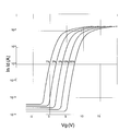
- 238000011156 evaluation Methods 0.000 description 3
- 230000000670 limiting effect Effects 0.000 description 3
- 229910052759 nickel Inorganic materials 0.000 description 3
- 125000004433 nitrogen atom Chemical group N* 0.000 description 3
- SOWBFZRMHSNYGE-UHFFFAOYSA-N oxamic acid Chemical compound NC(=O)C(O)=O SOWBFZRMHSNYGE-UHFFFAOYSA-N 0.000 description 3
- 229920001721 polyimide Polymers 0.000 description 3
- BDERNNFJNOPAEC-UHFFFAOYSA-N propan-1-ol Chemical compound CCCO BDERNNFJNOPAEC-UHFFFAOYSA-N 0.000 description 3
- 238000006722 reduction reaction Methods 0.000 description 3
- 239000011347 resin Substances 0.000 description 3
- 229920005989 resin Polymers 0.000 description 3
- 239000011342 resin composition Substances 0.000 description 3
- VSZWPYCFIRKVQL-UHFFFAOYSA-N selanylidenegallium;selenium Chemical compound [Se].[Se]=[Ga].[Se]=[Ga] VSZWPYCFIRKVQL-UHFFFAOYSA-N 0.000 description 3
- 239000007787 solid Substances 0.000 description 3
- WFKWXMTUELFFGS-UHFFFAOYSA-N tungsten Chemical compound [W] WFKWXMTUELFFGS-UHFFFAOYSA-N 0.000 description 3
- 239000010937 tungsten Substances 0.000 description 3
- 238000001039 wet etching Methods 0.000 description 3
- 229910052725 zinc Inorganic materials 0.000 description 3
- YVTHLONGBIQYBO-UHFFFAOYSA-N zinc indium(3+) oxygen(2-) Chemical compound [O--].[Zn++].[In+3] YVTHLONGBIQYBO-UHFFFAOYSA-N 0.000 description 3
- 229910052726 zirconium Inorganic materials 0.000 description 3
- KBPLFHHGFOOTCA-UHFFFAOYSA-N 1-Octanol Chemical compound CCCCCCCCO KBPLFHHGFOOTCA-UHFFFAOYSA-N 0.000 description 2
- LUBJCRLGQSPQNN-UHFFFAOYSA-N 1-Phenylurea Chemical compound NC(=O)NC1=CC=CC=C1 LUBJCRLGQSPQNN-UHFFFAOYSA-N 0.000 description 2
- RRQYJINTUHWNHW-UHFFFAOYSA-N 1-ethoxy-2-(2-ethoxyethoxy)ethane Chemical compound CCOCCOCCOCC RRQYJINTUHWNHW-UHFFFAOYSA-N 0.000 description 2
- BBMCTIGTTCKYKF-UHFFFAOYSA-N 1-heptanol Chemical compound CCCCCCCO BBMCTIGTTCKYKF-UHFFFAOYSA-N 0.000 description 2
- ARXJGSRGQADJSQ-UHFFFAOYSA-N 1-methoxypropan-2-ol Chemical compound COCC(C)O ARXJGSRGQADJSQ-UHFFFAOYSA-N 0.000 description 2
- IYZMXHQDXZKNCY-UHFFFAOYSA-N 1-n,1-n-diphenyl-4-n,4-n-bis[4-(n-phenylanilino)phenyl]benzene-1,4-diamine Chemical compound C1=CC=CC=C1N(C=1C=CC(=CC=1)N(C=1C=CC(=CC=1)N(C=1C=CC=CC=1)C=1C=CC=CC=1)C=1C=CC(=CC=1)N(C=1C=CC=CC=1)C=1C=CC=CC=1)C1=CC=CC=C1 IYZMXHQDXZKNCY-UHFFFAOYSA-N 0.000 description 2
- CETWDUZRCINIHU-UHFFFAOYSA-N 2-heptanol Chemical compound CCCCCC(C)O CETWDUZRCINIHU-UHFFFAOYSA-N 0.000 description 2
- PFNHSEQQEPMLNI-UHFFFAOYSA-N 2-methyl-1-pentanol Chemical compound CCCC(C)CO PFNHSEQQEPMLNI-UHFFFAOYSA-N 0.000 description 2
- WFRBDWRZVBPBDO-UHFFFAOYSA-N 2-methyl-2-pentanol Chemical compound CCCC(C)(C)O WFRBDWRZVBPBDO-UHFFFAOYSA-N 0.000 description 2
- HONWGFNQCPRRFM-UHFFFAOYSA-N 2-n-(3-methylphenyl)-1-n,1-n,2-n-triphenylbenzene-1,2-diamine Chemical compound CC1=CC=CC(N(C=2C=CC=CC=2)C=2C(=CC=CC=2)N(C=2C=CC=CC=2)C=2C=CC=CC=2)=C1 HONWGFNQCPRRFM-UHFFFAOYSA-N 0.000 description 2
- NGDNVOAEIVQRFH-UHFFFAOYSA-N 2-nonanol Chemical compound CCCCCCCC(C)O NGDNVOAEIVQRFH-UHFFFAOYSA-N 0.000 description 2
- PRNCMAKCNVRZFX-UHFFFAOYSA-N 3,7-dimethyloctan-1-ol Chemical compound CC(C)CCCC(C)CCO PRNCMAKCNVRZFX-UHFFFAOYSA-N 0.000 description 2
- MXLMTQWGSQIYOW-UHFFFAOYSA-N 3-methyl-2-butanol Chemical compound CC(C)C(C)O MXLMTQWGSQIYOW-UHFFFAOYSA-N 0.000 description 2
- FRDAATYAJDYRNW-UHFFFAOYSA-N 3-methyl-3-pentanol Chemical compound CCC(C)(O)CC FRDAATYAJDYRNW-UHFFFAOYSA-N 0.000 description 2
- IWTBVKIGCDZRPL-UHFFFAOYSA-N 3-methylpentanol Chemical compound CCC(C)CCO IWTBVKIGCDZRPL-UHFFFAOYSA-N 0.000 description 2
- VATRWWPJWVCZTA-UHFFFAOYSA-N 3-oxo-n-[2-(trifluoromethyl)phenyl]butanamide Chemical compound CC(=O)CC(=O)NC1=CC=CC=C1C(F)(F)F VATRWWPJWVCZTA-UHFFFAOYSA-N 0.000 description 2
- YEJRWHAVMIAJKC-UHFFFAOYSA-N 4-Butyrolactone Chemical compound O=C1CCCO1 YEJRWHAVMIAJKC-UHFFFAOYSA-N 0.000 description 2
- BKQICAFAUMRYLZ-UHFFFAOYSA-N 4-methylheptan-3-ol Chemical compound CCCC(C)C(O)CC BKQICAFAUMRYLZ-UHFFFAOYSA-N 0.000 description 2
- FCOUHTHQYOMLJT-UHFFFAOYSA-N 6-methylheptan-2-ol Chemical compound CC(C)CCCC(C)O FCOUHTHQYOMLJT-UHFFFAOYSA-N 0.000 description 2
- VFUDMQLBKNMONU-UHFFFAOYSA-N 9-[4-(4-carbazol-9-ylphenyl)phenyl]carbazole Chemical group C12=CC=CC=C2C2=CC=CC=C2N1C1=CC=C(C=2C=CC(=CC=2)N2C3=CC=CC=C3C3=CC=CC=C32)C=C1 VFUDMQLBKNMONU-UHFFFAOYSA-N 0.000 description 2
- DLFVBJFMPXGRIB-UHFFFAOYSA-N Acetamide Chemical compound CC(N)=O DLFVBJFMPXGRIB-UHFFFAOYSA-N 0.000 description 2
- 229910001316 Ag alloy Inorganic materials 0.000 description 2
- IJGRMHOSHXDMSA-UHFFFAOYSA-N Atomic nitrogen Chemical compound N#N IJGRMHOSHXDMSA-UHFFFAOYSA-N 0.000 description 2
- KXDAEFPNCMNJSK-UHFFFAOYSA-N Benzamide Chemical compound NC(=O)C1=CC=CC=C1 KXDAEFPNCMNJSK-UHFFFAOYSA-N 0.000 description 2
- ZAFNJMIOTHYJRJ-UHFFFAOYSA-N Diisopropyl ether Chemical compound CC(C)OC(C)C ZAFNJMIOTHYJRJ-UHFFFAOYSA-N 0.000 description 2
- IAZDPXIOMUYVGZ-UHFFFAOYSA-N Dimethylsulphoxide Chemical compound CS(C)=O IAZDPXIOMUYVGZ-UHFFFAOYSA-N 0.000 description 2
- RZKSECIXORKHQS-UHFFFAOYSA-N Heptan-3-ol Chemical compound CCCCC(O)CC RZKSECIXORKHQS-UHFFFAOYSA-N 0.000 description 2
- UFHFLCQGNIYNRP-UHFFFAOYSA-N Hydrogen Chemical compound [H][H] UFHFLCQGNIYNRP-UHFFFAOYSA-N 0.000 description 2
- KFZMGEQAYNKOFK-UHFFFAOYSA-N Isopropanol Chemical compound CC(C)O KFZMGEQAYNKOFK-UHFFFAOYSA-N 0.000 description 2
- 229910017625 MgSiO Inorganic materials 0.000 description 2
- ZOKXTWBITQBERF-UHFFFAOYSA-N Molybdenum Chemical compound [Mo] ZOKXTWBITQBERF-UHFFFAOYSA-N 0.000 description 2
- LRHPLDYGYMQRHN-UHFFFAOYSA-N N-Butanol Chemical compound CCCCO LRHPLDYGYMQRHN-UHFFFAOYSA-N 0.000 description 2
- AMQJEAYHLZJPGS-UHFFFAOYSA-N N-Pentanol Chemical compound CCCCCO AMQJEAYHLZJPGS-UHFFFAOYSA-N 0.000 description 2
- XGEGHDBEHXKFPX-UHFFFAOYSA-N N-methyl urea Chemical compound CNC(N)=O XGEGHDBEHXKFPX-UHFFFAOYSA-N 0.000 description 2
- 229910000990 Ni alloy Inorganic materials 0.000 description 2
- 229910019142 PO4 Inorganic materials 0.000 description 2
- NBIIXXVUZAFLBC-UHFFFAOYSA-N Phosphoric acid Chemical compound OP(O)(O)=O NBIIXXVUZAFLBC-UHFFFAOYSA-N 0.000 description 2
- JUJWROOIHBZHMG-UHFFFAOYSA-N Pyridine Chemical compound C1=CC=NC=C1 JUJWROOIHBZHMG-UHFFFAOYSA-N 0.000 description 2
- 229910020923 Sn-O Inorganic materials 0.000 description 2
- QAOWNCQODCNURD-UHFFFAOYSA-N Sulfuric acid Chemical compound OS(O)(=O)=O QAOWNCQODCNURD-UHFFFAOYSA-N 0.000 description 2
- DKGAVHZHDRPRBM-UHFFFAOYSA-N Tert-Butanol Chemical compound CC(C)(C)O DKGAVHZHDRPRBM-UHFFFAOYSA-N 0.000 description 2
- 239000007983 Tris buffer Substances 0.000 description 2
- XSQUKJJJFZCRTK-UHFFFAOYSA-N Urea Chemical compound NC(N)=O XSQUKJJJFZCRTK-UHFFFAOYSA-N 0.000 description 2
- 229910003363 ZnMgO Inorganic materials 0.000 description 2
- NIXOWILDQLNWCW-UHFFFAOYSA-N acrylic acid group Chemical group C(C=C)(=O)O NIXOWILDQLNWCW-UHFFFAOYSA-N 0.000 description 2
- BVCZEBOGSOYJJT-UHFFFAOYSA-N ammonium carbamate Chemical compound [NH4+].NC([O-])=O BVCZEBOGSOYJJT-UHFFFAOYSA-N 0.000 description 2
- 238000000231 atomic layer deposition Methods 0.000 description 2
- 230000008901 benefit Effects 0.000 description 2
- 230000005540 biological transmission Effects 0.000 description 2
- 235000010290 biphenyl Nutrition 0.000 description 2
- 239000004202 carbamide Substances 0.000 description 2
- BVKZGUZCCUSVTD-UHFFFAOYSA-N carbonic acid Chemical class OC(O)=O BVKZGUZCCUSVTD-UHFFFAOYSA-N 0.000 description 2
- KXDHJXZQYSOELW-UHFFFAOYSA-N carbonic acid monoamide Natural products NC(O)=O KXDHJXZQYSOELW-UHFFFAOYSA-N 0.000 description 2
- 239000000470 constituent Substances 0.000 description 2
- XCJYREBRNVKWGJ-UHFFFAOYSA-N copper(II) phthalocyanine Chemical compound [Cu+2].C12=CC=CC=C2C(N=C2[N-]C(C3=CC=CC=C32)=N2)=NC1=NC([C]1C=CC=CC1=1)=NC=1N=C1[C]3C=CC=CC3=C2[N-]1 XCJYREBRNVKWGJ-UHFFFAOYSA-N 0.000 description 2
- JHIVVAPYMSGYDF-UHFFFAOYSA-N cyclohexanone Chemical compound O=C1CCCCC1 JHIVVAPYMSGYDF-UHFFFAOYSA-N 0.000 description 2
- WCGGWVOVFQNRRS-UHFFFAOYSA-N dichloroacetamide Chemical compound NC(=O)C(Cl)Cl WCGGWVOVFQNRRS-UHFFFAOYSA-N 0.000 description 2
- 229940019778 diethylene glycol diethyl ether Drugs 0.000 description 2
- 238000009826 distribution Methods 0.000 description 2
- 238000001035 drying Methods 0.000 description 2
- 238000005538 encapsulation Methods 0.000 description 2
- LZCLXQDLBQLTDK-UHFFFAOYSA-N ethyl 2-hydroxypropanoate Chemical compound CCOC(=O)C(C)O LZCLXQDLBQLTDK-UHFFFAOYSA-N 0.000 description 2
- 230000005281 excited state Effects 0.000 description 2
- 230000001747 exhibiting effect Effects 0.000 description 2
- 238000010304 firing Methods 0.000 description 2
- 230000005283 ground state Effects 0.000 description 2
- 230000020169 heat generation Effects 0.000 description 2
- ZSIAUFGUXNUGDI-UHFFFAOYSA-N hexan-1-ol Chemical compound CCCCCCO ZSIAUFGUXNUGDI-UHFFFAOYSA-N 0.000 description 2
- AMWRITDGCCNYAT-UHFFFAOYSA-L hydroxy(oxo)manganese;manganese Chemical compound [Mn].O[Mn]=O.O[Mn]=O AMWRITDGCCNYAT-UHFFFAOYSA-L 0.000 description 2
- APFVFJFRJDLVQX-UHFFFAOYSA-N indium atom Chemical compound [In] APFVFJFRJDLVQX-UHFFFAOYSA-N 0.000 description 2
- 238000007641 inkjet printing Methods 0.000 description 2
- PHTQWCKDNZKARW-UHFFFAOYSA-N isoamylol Chemical compound CC(C)CCO PHTQWCKDNZKARW-UHFFFAOYSA-N 0.000 description 2
- 238000010030 laminating Methods 0.000 description 2
- 229910052746 lanthanum Inorganic materials 0.000 description 2
- 239000005300 metallic glass Substances 0.000 description 2
- 150000002739 metals Chemical class 0.000 description 2
- GTCAXTIRRLKXRU-UHFFFAOYSA-N methyl carbamate Chemical compound COC(N)=O GTCAXTIRRLKXRU-UHFFFAOYSA-N 0.000 description 2
- 239000003595 mist Substances 0.000 description 2
- 239000011733 molybdenum Substances 0.000 description 2
- IBHBKWKFFTZAHE-UHFFFAOYSA-N n-[4-[4-(n-naphthalen-1-ylanilino)phenyl]phenyl]-n-phenylnaphthalen-1-amine Chemical group C1=CC=CC=C1N(C=1C2=CC=CC=C2C=CC=1)C1=CC=C(C=2C=CC(=CC=2)N(C=2C=CC=CC=2)C=2C3=CC=CC=C3C=CC=2)C=C1 IBHBKWKFFTZAHE-UHFFFAOYSA-N 0.000 description 2
- 239000002105 nanoparticle Substances 0.000 description 2
- 229910052758 niobium Inorganic materials 0.000 description 2
- GUCVJGMIXFAOAE-UHFFFAOYSA-N niobium atom Chemical compound [Nb] GUCVJGMIXFAOAE-UHFFFAOYSA-N 0.000 description 2
- ZWRUINPWMLAQRD-UHFFFAOYSA-N nonan-1-ol Chemical compound CCCCCCCCCO ZWRUINPWMLAQRD-UHFFFAOYSA-N 0.000 description 2
- SJWFXCIHNDVPSH-UHFFFAOYSA-N octan-2-ol Chemical compound CCCCCCC(C)O SJWFXCIHNDVPSH-UHFFFAOYSA-N 0.000 description 2
- YRZZLAGRKZIJJI-UHFFFAOYSA-N oxyvanadium phthalocyanine Chemical compound [V+2]=O.C12=CC=CC=C2C(N=C2[N-]C(C3=CC=CC=C32)=N2)=NC1=NC([C]1C=CC=CC1=1)=NC=1N=C1[C]3C=CC=CC3=C2[N-]1 YRZZLAGRKZIJJI-UHFFFAOYSA-N 0.000 description 2
- JYVLIDXNZAXMDK-UHFFFAOYSA-N pentan-2-ol Chemical compound CCCC(C)O JYVLIDXNZAXMDK-UHFFFAOYSA-N 0.000 description 2
- AQIXEPGDORPWBJ-UHFFFAOYSA-N pentan-3-ol Chemical compound CCC(O)CC AQIXEPGDORPWBJ-UHFFFAOYSA-N 0.000 description 2
- 235000021317 phosphate Nutrition 0.000 description 2
- 238000000206 photolithography Methods 0.000 description 2
- 238000009832 plasma treatment Methods 0.000 description 2
- 239000002096 quantum dot Substances 0.000 description 2
- 239000002994 raw material Substances 0.000 description 2
- 239000003870 refractory metal Substances 0.000 description 2
- 230000002940 repellent Effects 0.000 description 2
- 239000005871 repellent Substances 0.000 description 2
- 229910052706 scandium Inorganic materials 0.000 description 2
- 229910021332 silicide Inorganic materials 0.000 description 2
- FVBUAEGBCNSCDD-UHFFFAOYSA-N silicide(4-) Chemical compound [Si-4] FVBUAEGBCNSCDD-UHFFFAOYSA-N 0.000 description 2
- 239000011780 sodium chloride Substances 0.000 description 2
- 238000004528 spin coating Methods 0.000 description 2
- 238000005477 sputtering target Methods 0.000 description 2
- HHVIBTZHLRERCL-UHFFFAOYSA-N sulfonyldimethane Chemical compound CS(C)(=O)=O HHVIBTZHLRERCL-UHFFFAOYSA-N 0.000 description 2
- 238000012546 transfer Methods 0.000 description 2
- VOITXYVAKOUIBA-UHFFFAOYSA-N triethylaluminium Chemical compound CC[Al](CC)CC VOITXYVAKOUIBA-UHFFFAOYSA-N 0.000 description 2
- XCZXGTMEAKBVPV-UHFFFAOYSA-N trimethylgallium Chemical compound C[Ga](C)C XCZXGTMEAKBVPV-UHFFFAOYSA-N 0.000 description 2
- IBEFSUTVZWZJEL-UHFFFAOYSA-N trimethylindium Chemical compound C[In](C)C IBEFSUTVZWZJEL-UHFFFAOYSA-N 0.000 description 2
- ZVWKZXLXHLZXLS-UHFFFAOYSA-N zirconium nitride Chemical compound [Zr]#N ZVWKZXLXHLZXLS-UHFFFAOYSA-N 0.000 description 2
- 239000001618 (3R)-3-methylpentan-1-ol Substances 0.000 description 1
- ULUZGMIUTMRARO-UHFFFAOYSA-N (carbamoylamino)urea Chemical compound NC(=O)NNC(N)=O ULUZGMIUTMRARO-UHFFFAOYSA-N 0.000 description 1
- QYGBYAQGBVHMDD-XQRVVYSFSA-N (z)-2-cyano-3-thiophen-2-ylprop-2-enoic acid Chemical compound OC(=O)C(\C#N)=C/C1=CC=CS1 QYGBYAQGBVHMDD-XQRVVYSFSA-N 0.000 description 1
- BSSNZUFKXJJCBG-UPHRSURJSA-N (z)-but-2-enediamide Chemical compound NC(=O)\C=C/C(N)=O BSSNZUFKXJJCBG-UPHRSURJSA-N 0.000 description 1
- AVQQQNCBBIEMEU-UHFFFAOYSA-N 1,1,3,3-tetramethylurea Chemical compound CN(C)C(=O)N(C)C AVQQQNCBBIEMEU-UHFFFAOYSA-N 0.000 description 1
- YBBLOADPFWKNGS-UHFFFAOYSA-N 1,1-dimethylurea Chemical compound CN(C)C(N)=O YBBLOADPFWKNGS-UHFFFAOYSA-N 0.000 description 1
- KNIKDPRISVIPBU-UHFFFAOYSA-N 1,2-dichloro-4-[isocyano-(4-methylphenyl)sulfonylmethyl]benzene Chemical compound C1=CC(C)=CC=C1S(=O)(=O)C([N+]#[C-])C1=CC=C(Cl)C(Cl)=C1 KNIKDPRISVIPBU-UHFFFAOYSA-N 0.000 description 1
- 239000005968 1-Decanol Substances 0.000 description 1
- LXQMHOKEXZETKB-UHFFFAOYSA-N 1-amino-2-methylpropan-2-ol Chemical compound CC(C)(O)CN LXQMHOKEXZETKB-UHFFFAOYSA-N 0.000 description 1
- XOYZGLGJSAZOAG-UHFFFAOYSA-N 1-n,1-n,4-n-triphenyl-4-n-[4-[4-(n-[4-(n-phenylanilino)phenyl]anilino)phenyl]phenyl]benzene-1,4-diamine Chemical group C1=CC=CC=C1N(C=1C=CC(=CC=1)N(C=1C=CC=CC=1)C=1C=CC(=CC=1)C=1C=CC(=CC=1)N(C=1C=CC=CC=1)C=1C=CC(=CC=1)N(C=1C=CC=CC=1)C=1C=CC=CC=1)C1=CC=CC=C1 XOYZGLGJSAZOAG-UHFFFAOYSA-N 0.000 description 1
- SPDPTFAJSFKAMT-UHFFFAOYSA-N 1-n-[4-[4-(n-[4-(3-methyl-n-(3-methylphenyl)anilino)phenyl]anilino)phenyl]phenyl]-4-n,4-n-bis(3-methylphenyl)-1-n-phenylbenzene-1,4-diamine Chemical compound CC1=CC=CC(N(C=2C=CC(=CC=2)N(C=2C=CC=CC=2)C=2C=CC(=CC=2)C=2C=CC(=CC=2)N(C=2C=CC=CC=2)C=2C=CC(=CC=2)N(C=2C=C(C)C=CC=2)C=2C=C(C)C=CC=2)C=2C=C(C)C=CC=2)=C1 SPDPTFAJSFKAMT-UHFFFAOYSA-N 0.000 description 1
- VSNHCAURESNICA-NJFSPNSNSA-N 1-oxidanylurea Chemical compound N[14C](=O)NO VSNHCAURESNICA-NJFSPNSNSA-N 0.000 description 1
- MQRCTQVBZYBPQE-UHFFFAOYSA-N 189363-47-1 Chemical compound C1=CC=CC=C1N(C=1C=C2C3(C4=CC(=CC=C4C2=CC=1)N(C=1C=CC=CC=1)C=1C=CC=CC=1)C1=CC(=CC=C1C1=CC=C(C=C13)N(C=1C=CC=CC=1)C=1C=CC=CC=1)N(C=1C=CC=CC=1)C=1C=CC=CC=1)C1=CC=CC=C1 MQRCTQVBZYBPQE-UHFFFAOYSA-N 0.000 description 1
- UPQQXPKAYZYUKO-UHFFFAOYSA-N 2,2,2-trichloroacetamide Chemical compound OC(=N)C(Cl)(Cl)Cl UPQQXPKAYZYUKO-UHFFFAOYSA-N 0.000 description 1
- NRKYWOKHZRQRJR-UHFFFAOYSA-N 2,2,2-trifluoroacetamide Chemical compound NC(=O)C(F)(F)F NRKYWOKHZRQRJR-UHFFFAOYSA-N 0.000 description 1
- KQTOYEUYHXUEDB-UHFFFAOYSA-N 2,2,3,3,3-pentafluoropropanamide Chemical compound NC(=O)C(F)(F)C(F)(F)F KQTOYEUYHXUEDB-UHFFFAOYSA-N 0.000 description 1
- WBGBQSRNXPVFDB-UHFFFAOYSA-N 2,2,3,3,4,4,4-heptafluorobutan-1-amine Chemical compound NCC(F)(F)C(F)(F)C(F)(F)F WBGBQSRNXPVFDB-UHFFFAOYSA-N 0.000 description 1
- WBIDVKZMUARURD-UHFFFAOYSA-N 2,2-dimethoxypropanamide Chemical compound COC(C)(OC)C(N)=O WBIDVKZMUARURD-UHFFFAOYSA-N 0.000 description 1
- HMSVXZJWPVIVIV-UHFFFAOYSA-N 2,2-dimethylpentan-3-ol Chemical compound CCC(O)C(C)(C)C HMSVXZJWPVIVIV-UHFFFAOYSA-N 0.000 description 1
- WPWWHXPRJFDTTJ-UHFFFAOYSA-N 2,3,4,5,6-pentafluorobenzamide Chemical compound NC(=O)C1=C(F)C(F)=C(F)C(F)=C1F WPWWHXPRJFDTTJ-UHFFFAOYSA-N 0.000 description 1
- RFZHJHSNHYIRNE-UHFFFAOYSA-N 2,3-dimethylpentan-3-ol Chemical compound CCC(C)(O)C(C)C RFZHJHSNHYIRNE-UHFFFAOYSA-N 0.000 description 1
- ZNRVRWHPZZOTIE-UHFFFAOYSA-N 2,4,4-trimethylpentan-1-ol Chemical compound OCC(C)CC(C)(C)C ZNRVRWHPZZOTIE-UHFFFAOYSA-N 0.000 description 1
- BAYAKMPRFGNNFW-UHFFFAOYSA-N 2,4-dimethylpentan-3-ol Chemical compound CC(C)C(O)C(C)C BAYAKMPRFGNNFW-UHFFFAOYSA-N 0.000 description 1
- WOFPPJOZXUTRAU-UHFFFAOYSA-N 2-Ethyl-1-hexanol Natural products CCCCC(O)CCC WOFPPJOZXUTRAU-UHFFFAOYSA-N 0.000 description 1
- WKNMKGVLOWGGOU-UHFFFAOYSA-N 2-aminoacetamide;hydron;chloride Chemical compound Cl.NCC(N)=O WKNMKGVLOWGGOU-UHFFFAOYSA-N 0.000 description 1
- BITBMHVXCILUEX-UHFFFAOYSA-N 2-chloroethylurea Chemical compound NC(=O)NCCCl BITBMHVXCILUEX-UHFFFAOYSA-N 0.000 description 1
- ZNQVEEAIQZEUHB-UHFFFAOYSA-N 2-ethoxyethanol Chemical compound CCOCCO ZNQVEEAIQZEUHB-UHFFFAOYSA-N 0.000 description 1
- YIWUKEYIRIRTPP-UHFFFAOYSA-N 2-ethylhexan-1-ol Chemical compound CCCCC(CC)CO YIWUKEYIRIRTPP-UHFFFAOYSA-N 0.000 description 1
- FVTWJXMFYOXOKK-UHFFFAOYSA-N 2-fluoroacetamide Chemical compound NC(=O)CF FVTWJXMFYOXOKK-UHFFFAOYSA-N 0.000 description 1
- CLAHOZSYMRNIPY-UHFFFAOYSA-N 2-hydroxyethylurea Chemical compound NC(=O)NCCO CLAHOZSYMRNIPY-UHFFFAOYSA-N 0.000 description 1
- ISTJMQSHILQAEC-UHFFFAOYSA-N 2-methyl-3-pentanol Chemical compound CCC(O)C(C)C ISTJMQSHILQAEC-UHFFFAOYSA-N 0.000 description 1
- KRIMXCDMVRMCTC-UHFFFAOYSA-N 2-methylhexan-2-ol Chemical compound CCCCC(C)(C)O KRIMXCDMVRMCTC-UHFFFAOYSA-N 0.000 description 1
- RGRUUTLDBCWYBL-UHFFFAOYSA-N 2-methylhexan-3-ol Chemical compound CCCC(O)C(C)C RGRUUTLDBCWYBL-UHFFFAOYSA-N 0.000 description 1
- QZTQQBIGSZWRGI-UHFFFAOYSA-N 2-n',7-n'-bis(3-methylphenyl)-2-n',7-n'-diphenyl-9,9'-spirobi[fluorene]-2',7'-diamine Chemical compound CC1=CC=CC(N(C=2C=CC=CC=2)C=2C=C3C4(C5=CC=CC=C5C5=CC=CC=C54)C4=CC(=CC=C4C3=CC=2)N(C=2C=CC=CC=2)C=2C=C(C)C=CC=2)=C1 QZTQQBIGSZWRGI-UHFFFAOYSA-N 0.000 description 1
- LASHFHLFDRTERB-UHFFFAOYSA-N 2-propylpentan-1-ol Chemical compound CCCC(CO)CCC LASHFHLFDRTERB-UHFFFAOYSA-N 0.000 description 1
- BODRLKRKPXBDBN-UHFFFAOYSA-N 3,5,5-Trimethyl-1-hexanol Chemical compound OCCC(C)CC(C)(C)C BODRLKRKPXBDBN-UHFFFAOYSA-N 0.000 description 1
- YNOPIKHMZIOWHS-UHFFFAOYSA-N 3,5-bis(trifluoromethyl)benzamide Chemical compound NC(=O)C1=CC(C(F)(F)F)=CC(C(F)(F)F)=C1 YNOPIKHMZIOWHS-UHFFFAOYSA-N 0.000 description 1
- DLHQZZUEERVIGQ-UHFFFAOYSA-N 3,7-dimethyl-3-octanol Chemical compound CCC(C)(O)CCCC(C)C DLHQZZUEERVIGQ-UHFFFAOYSA-N 0.000 description 1
- TVMBOHMLKCZFFW-UHFFFAOYSA-N 3-N,6-N,9-triphenyl-3-N,6-N-bis(9-phenylcarbazol-3-yl)carbazole-3,6-diamine Chemical compound C1=CC=CC=C1N(C=1C=C2C3=CC(=CC=C3N(C=3C=CC=CC=3)C2=CC=1)N(C=1C=CC=CC=1)C=1C=C2C3=CC=CC=C3N(C=3C=CC=CC=3)C2=CC=1)C1=CC=C(N(C=2C=CC=CC=2)C=2C3=CC=CC=2)C3=C1 TVMBOHMLKCZFFW-UHFFFAOYSA-N 0.000 description 1
- NMRPBPVERJPACX-QMMMGPOBSA-N 3-Octanol Natural products CCCCC[C@@H](O)CC NMRPBPVERJPACX-QMMMGPOBSA-N 0.000 description 1
- GAGJMOQGABUOBK-UHFFFAOYSA-N 3-aminopropanamide;hydrochloride Chemical compound Cl.NCCC(N)=O GAGJMOQGABUOBK-UHFFFAOYSA-N 0.000 description 1
- DBIVLAVBOICUQX-UHFFFAOYSA-N 3-bromopropanamide Chemical compound NC(=O)CCBr DBIVLAVBOICUQX-UHFFFAOYSA-N 0.000 description 1
- HEQYMZTUSVDQBW-UHFFFAOYSA-N 3-ethyl-2,2-dimethylpentan-1-ol Chemical compound CCC(CC)C(C)(C)CO HEQYMZTUSVDQBW-UHFFFAOYSA-N 0.000 description 1
- XKIRHOWVQWCYBT-UHFFFAOYSA-N 3-ethylpentan-3-ol Chemical compound CCC(O)(CC)CC XKIRHOWVQWCYBT-UHFFFAOYSA-N 0.000 description 1
- ZXNBBWHRUSXUFZ-UHFFFAOYSA-N 3-methyl-2-pentanol Chemical compound CCC(C)C(C)O ZXNBBWHRUSXUFZ-UHFFFAOYSA-N 0.000 description 1
- LDMRLRNXHLPZJN-UHFFFAOYSA-N 3-propoxypropan-1-ol Chemical compound CCCOCCCO LDMRLRNXHLPZJN-UHFFFAOYSA-N 0.000 description 1
- OIBKGNPMOMMSSI-UHFFFAOYSA-N 4,4-dimethylpentan-2-ol Chemical compound CC(O)CC(C)(C)C OIBKGNPMOMMSSI-UHFFFAOYSA-N 0.000 description 1
- DTDMYWXTWWFLGJ-JTQLQIEISA-N 4-Decanol Natural products CCCCCC[C@@H](O)CCC DTDMYWXTWWFLGJ-JTQLQIEISA-N 0.000 description 1
- CAERPAFTLPIDJT-UHFFFAOYSA-N 4-amino-2,3,5,6-tetrafluorobenzamide Chemical compound NC(=O)C1=C(F)C(F)=C(N)C(F)=C1F CAERPAFTLPIDJT-UHFFFAOYSA-N 0.000 description 1
- AZFHXIBNMPIGOD-UHFFFAOYSA-N 4-hydroxypent-3-en-2-one iridium Chemical compound [Ir].CC(O)=CC(C)=O.CC(O)=CC(C)=O.CC(O)=CC(C)=O AZFHXIBNMPIGOD-UHFFFAOYSA-N 0.000 description 1
- WVYWICLMDOOCFB-UHFFFAOYSA-N 4-methyl-2-pentanol Chemical compound CC(C)CC(C)O WVYWICLMDOOCFB-UHFFFAOYSA-N 0.000 description 1
- PCWGTDULNUVNBN-UHFFFAOYSA-N 4-methylpentan-1-ol Chemical compound CC(C)CCCO PCWGTDULNUVNBN-UHFFFAOYSA-N 0.000 description 1
- KLNDKWAYVMOOFU-UHFFFAOYSA-N 4-n-[9,10-bis(2-phenylphenyl)anthracen-2-yl]-1-n,1-n,4-n-triphenylbenzene-1,4-diamine Chemical compound C1=CC=CC=C1N(C=1C=CC(=CC=1)N(C=1C=CC=CC=1)C=1C=C2C(C=3C(=CC=CC=3)C=3C=CC=CC=3)=C3C=CC=CC3=C(C=3C(=CC=CC=3)C=3C=CC=CC=3)C2=CC=1)C1=CC=CC=C1 KLNDKWAYVMOOFU-UHFFFAOYSA-N 0.000 description 1
- ZVHAANQOQZVVFD-UHFFFAOYSA-N 5-methylhexan-1-ol Chemical compound CC(C)CCCCO ZVHAANQOQZVVFD-UHFFFAOYSA-N 0.000 description 1
- ZDVJGWXFXGJSIU-UHFFFAOYSA-N 5-methylhexan-2-ol Chemical compound CC(C)CCC(C)O ZDVJGWXFXGJSIU-UHFFFAOYSA-N 0.000 description 1
- TYGSHIPXFUQBJO-UHFFFAOYSA-N 5-n,5-n,11-n,11-n-tetrakis(4-methylphenyl)tetracene-5,11-diamine Chemical compound C1=CC(C)=CC=C1N(C=1C2=CC3=CC=CC=C3C(N(C=3C=CC(C)=CC=3)C=3C=CC(C)=CC=3)=C2C=C2C=CC=CC2=1)C1=CC=C(C)C=C1 TYGSHIPXFUQBJO-UHFFFAOYSA-N 0.000 description 1
- UJTTUOLQLCQZEA-UHFFFAOYSA-N 9h-fluoren-9-ylmethyl n-(4-hydroxybutyl)carbamate Chemical compound C1=CC=C2C(COC(=O)NCCCCO)C3=CC=CC=C3C2=C1 UJTTUOLQLCQZEA-UHFFFAOYSA-N 0.000 description 1
- HRPVXLWXLXDGHG-UHFFFAOYSA-N Acrylamide Chemical compound NC(=O)C=C HRPVXLWXLXDGHG-UHFFFAOYSA-N 0.000 description 1
- GVNWZKBFMFUVNX-UHFFFAOYSA-N Adipamide Chemical compound NC(=O)CCCCC(N)=O GVNWZKBFMFUVNX-UHFFFAOYSA-N 0.000 description 1
- 229910001148 Al-Li alloy Inorganic materials 0.000 description 1
- ZKHISQHQYQCSJE-UHFFFAOYSA-N C1=CC=CC=C1N(C=1C=CC(=CC=1)N(C=1C=CC=CC=1)C=1C=C(C=C(C=1)N(C=1C=CC=CC=1)C=1C=CC(=CC=1)N(C=1C=CC=CC=1)C=1C=CC=CC=1)N(C=1C=CC=CC=1)C=1C=CC(=CC=1)N(C=1C=CC=CC=1)C=1C=CC=CC=1)C1=CC=CC=C1 Chemical compound C1=CC=CC=C1N(C=1C=CC(=CC=1)N(C=1C=CC=CC=1)C=1C=C(C=C(C=1)N(C=1C=CC=CC=1)C=1C=CC(=CC=1)N(C=1C=CC=CC=1)C=1C=CC=CC=1)N(C=1C=CC=CC=1)C=1C=CC(=CC=1)N(C=1C=CC=CC=1)C=1C=CC=CC=1)C1=CC=CC=C1 ZKHISQHQYQCSJE-UHFFFAOYSA-N 0.000 description 1
- OYPRJOBELJOOCE-UHFFFAOYSA-N Calcium Chemical compound [Ca] OYPRJOBELJOOCE-UHFFFAOYSA-N 0.000 description 1
- KZBUYRJDOAKODT-UHFFFAOYSA-N Chlorine Chemical compound ClCl KZBUYRJDOAKODT-UHFFFAOYSA-N 0.000 description 1
- RYGMFSIKBFXOCR-UHFFFAOYSA-N Copper Chemical compound [Cu] RYGMFSIKBFXOCR-UHFFFAOYSA-N 0.000 description 1
- 229910000881 Cu alloy Inorganic materials 0.000 description 1
- 229910000570 Cupronickel Inorganic materials 0.000 description 1
- 229910002482 Cu–Ni Inorganic materials 0.000 description 1
- HXQPUEQDBSPXTE-UHFFFAOYSA-N Diisobutylcarbinol Chemical compound CC(C)CC(O)CC(C)C HXQPUEQDBSPXTE-UHFFFAOYSA-N 0.000 description 1
- MYMOFIZGZYHOMD-UHFFFAOYSA-N Dioxygen Chemical compound O=O MYMOFIZGZYHOMD-UHFFFAOYSA-N 0.000 description 1
- 239000004593 Epoxy Substances 0.000 description 1
- JOYRKODLDBILNP-UHFFFAOYSA-N Ethyl urethane Chemical compound CCOC(N)=O JOYRKODLDBILNP-UHFFFAOYSA-N 0.000 description 1
- RYECOJGRJDOGPP-UHFFFAOYSA-N Ethylurea Chemical compound CCNC(N)=O RYECOJGRJDOGPP-UHFFFAOYSA-N 0.000 description 1
- 101710162828 Flavin-dependent thymidylate synthase Proteins 0.000 description 1
- JMASRVWKEDWRBT-UHFFFAOYSA-N Gallium nitride Chemical compound [Ga]#N JMASRVWKEDWRBT-UHFFFAOYSA-N 0.000 description 1
- SQSPRWMERUQXNE-UHFFFAOYSA-N Guanylurea Chemical compound NC(=N)NC(N)=O SQSPRWMERUQXNE-UHFFFAOYSA-N 0.000 description 1
- 206010021143 Hypoxia Diseases 0.000 description 1
- FYYHWMGAXLPEAU-UHFFFAOYSA-N Magnesium Chemical compound [Mg] FYYHWMGAXLPEAU-UHFFFAOYSA-N 0.000 description 1
- JLVVSXFLKOJNIY-UHFFFAOYSA-N Magnesium ion Chemical compound [Mg+2] JLVVSXFLKOJNIY-UHFFFAOYSA-N 0.000 description 1
- FXHOOIRPVKKKFG-UHFFFAOYSA-N N,N-Dimethylacetamide Chemical compound CN(C)C(C)=O FXHOOIRPVKKKFG-UHFFFAOYSA-N 0.000 description 1
- ZWXPDGCFMMFNRW-UHFFFAOYSA-N N-methylcaprolactam Chemical compound CN1CCCCCC1=O ZWXPDGCFMMFNRW-UHFFFAOYSA-N 0.000 description 1
- 229910002651 NO3 Inorganic materials 0.000 description 1
- NHNBFGGVMKEFGY-UHFFFAOYSA-N Nitrate Chemical compound [O-][N+]([O-])=O NHNBFGGVMKEFGY-UHFFFAOYSA-N 0.000 description 1
- GRYLNZFGIOXLOG-UHFFFAOYSA-N Nitric acid Chemical compound O[N+]([O-])=O GRYLNZFGIOXLOG-UHFFFAOYSA-N 0.000 description 1
- YIKSCQDJHCMVMK-UHFFFAOYSA-N Oxamide Chemical compound NC(=O)C(N)=O YIKSCQDJHCMVMK-UHFFFAOYSA-N 0.000 description 1
- 101710135409 Probable flavin-dependent thymidylate synthase Proteins 0.000 description 1
- YZCKVEUIGOORGS-IGMARMGPSA-N Protium Chemical compound [1H] YZCKVEUIGOORGS-IGMARMGPSA-N 0.000 description 1
- 229910052772 Samarium Inorganic materials 0.000 description 1
- 229910000676 Si alloy Inorganic materials 0.000 description 1
- BQCADISMDOOEFD-UHFFFAOYSA-N Silver Chemical compound [Ag] BQCADISMDOOEFD-UHFFFAOYSA-N 0.000 description 1
- 229910001069 Ti alloy Inorganic materials 0.000 description 1
- UATJOMSPNYCXIX-UHFFFAOYSA-N Trinitrobenzene Chemical compound [O-][N+](=O)C1=CC([N+]([O-])=O)=CC([N+]([O-])=O)=C1 UATJOMSPNYCXIX-UHFFFAOYSA-N 0.000 description 1
- PTFCDOFLOPIGGS-UHFFFAOYSA-N Zinc dication Chemical compound [Zn+2] PTFCDOFLOPIGGS-UHFFFAOYSA-N 0.000 description 1
- 229910007541 Zn O Inorganic materials 0.000 description 1
- FIAINKIUSZGVGX-DKWTVANSSA-N [(2s)-1-amino-1-oxopropan-2-yl]azanium;chloride Chemical compound Cl.C[C@H](N)C(N)=O FIAINKIUSZGVGX-DKWTVANSSA-N 0.000 description 1
- IUNNCDSJWDQYPW-DJWKRKHSSA-N [(z)-ethylideneamino]urea Chemical compound C\C=N/NC(N)=O IUNNCDSJWDQYPW-DJWKRKHSSA-N 0.000 description 1
- JFBZPFYRPYOZCQ-UHFFFAOYSA-N [Li].[Al] Chemical compound [Li].[Al] JFBZPFYRPYOZCQ-UHFFFAOYSA-N 0.000 description 1
- IZHOVLXXYOZDLW-UHFFFAOYSA-N [O-2].[Al+3].[Sn+4] Chemical compound [O-2].[Al+3].[Sn+4] IZHOVLXXYOZDLW-UHFFFAOYSA-N 0.000 description 1
- XHCLAFWTIXFWPH-UHFFFAOYSA-N [O-2].[O-2].[O-2].[O-2].[O-2].[V+5].[V+5] Chemical compound [O-2].[O-2].[O-2].[O-2].[O-2].[V+5].[V+5] XHCLAFWTIXFWPH-UHFFFAOYSA-N 0.000 description 1
- KKEYTLVFLSCKDE-UHFFFAOYSA-N [Sn+2]=O.[O-2].[Zn+2].[O-2] Chemical compound [Sn+2]=O.[O-2].[Zn+2].[O-2] KKEYTLVFLSCKDE-UHFFFAOYSA-N 0.000 description 1
- 238000010521 absorption reaction Methods 0.000 description 1
- CUJRVFIICFDLGR-UHFFFAOYSA-N acetylacetonate Chemical compound CC(=O)[CH-]C(C)=O CUJRVFIICFDLGR-UHFFFAOYSA-N 0.000 description 1
- 239000000853 adhesive Substances 0.000 description 1
- 230000001070 adhesive effect Effects 0.000 description 1
- 239000003513 alkali Substances 0.000 description 1
- 150000001339 alkali metal compounds Chemical class 0.000 description 1
- 125000002947 alkylene group Chemical group 0.000 description 1
- UQZIWOQVLUASCR-UHFFFAOYSA-N alumane;titanium Chemical compound [AlH3].[Ti] UQZIWOQVLUASCR-UHFFFAOYSA-N 0.000 description 1
- CSDREXVUYHZDNP-UHFFFAOYSA-N alumanylidynesilicon Chemical compound [Al].[Si] CSDREXVUYHZDNP-UHFFFAOYSA-N 0.000 description 1
- PNEYBMLMFCGWSK-UHFFFAOYSA-N aluminium oxide Inorganic materials [O-2].[O-2].[O-2].[Al+3].[Al+3] PNEYBMLMFCGWSK-UHFFFAOYSA-N 0.000 description 1
- 229910000147 aluminium phosphate Inorganic materials 0.000 description 1
- 239000005407 aluminoborosilicate glass Substances 0.000 description 1
- 239000005354 aluminosilicate glass Substances 0.000 description 1
- 239000003963 antioxidant agent Substances 0.000 description 1
- 230000003078 antioxidant effect Effects 0.000 description 1
- 238000013459 approach Methods 0.000 description 1
- 229920003235 aromatic polyamide Polymers 0.000 description 1
- 230000002238 attenuated effect Effects 0.000 description 1
- RJNJWHFSKNJCTB-UHFFFAOYSA-N benzylurea Chemical compound NC(=O)NCC1=CC=CC=C1 RJNJWHFSKNJCTB-UHFFFAOYSA-N 0.000 description 1
- 230000000903 blocking effect Effects 0.000 description 1
- KGBXLFKZBHKPEV-UHFFFAOYSA-N boric acid Chemical compound OB(O)O KGBXLFKZBHKPEV-UHFFFAOYSA-N 0.000 description 1
- 239000004327 boric acid Substances 0.000 description 1
- 150000001642 boronic acid derivatives Chemical class 0.000 description 1
- SKKTUOZKZKCGTB-UHFFFAOYSA-N butyl carbamate Chemical compound CCCCOC(N)=O SKKTUOZKZKCGTB-UHFFFAOYSA-N 0.000 description 1
- 125000000484 butyl group Chemical group [H]C([*])([H])C([H])([H])C([H])([H])C([H])([H])[H] 0.000 description 1
- MSZJEPVVQWJCIF-UHFFFAOYSA-N butylazanide Chemical compound CCCC[NH-] MSZJEPVVQWJCIF-UHFFFAOYSA-N 0.000 description 1
- CNWSQCLBDWYLAN-UHFFFAOYSA-N butylurea Chemical compound CCCCNC(N)=O CNWSQCLBDWYLAN-UHFFFAOYSA-N 0.000 description 1
- 229910052791 calcium Inorganic materials 0.000 description 1
- 125000000609 carbazolyl group Chemical group C1(=CC=CC=2C3=CC=CC=C3NC12)* 0.000 description 1
- 150000004649 carbonic acid derivatives Chemical class 0.000 description 1
- 230000015556 catabolic process Effects 0.000 description 1
- 239000010406 cathode material Substances 0.000 description 1
- 238000006243 chemical reaction Methods 0.000 description 1
- VXIVSQZSERGHQP-UHFFFAOYSA-N chloroacetamide Chemical compound NC(=O)CCl VXIVSQZSERGHQP-UHFFFAOYSA-N 0.000 description 1
- 238000007796 conventional method Methods 0.000 description 1
- 229910052802 copper Inorganic materials 0.000 description 1
- YOCUPQPZWBBYIX-UHFFFAOYSA-N copper nickel Chemical compound [Ni].[Cu] YOCUPQPZWBBYIX-UHFFFAOYSA-N 0.000 description 1
- PMHQVHHXPFUNSP-UHFFFAOYSA-M copper(1+);methylsulfanylmethane;bromide Chemical compound Br[Cu].CSC PMHQVHHXPFUNSP-UHFFFAOYSA-M 0.000 description 1
- DGJMPUGMZIKDRO-UHFFFAOYSA-N cyanoacetamide Chemical compound NC(=O)CC#N DGJMPUGMZIKDRO-UHFFFAOYSA-N 0.000 description 1
- HPXRVTGHNJAIIH-UHFFFAOYSA-N cyclohexanol Chemical compound OC1CCCCC1 HPXRVTGHNJAIIH-UHFFFAOYSA-N 0.000 description 1
- WUESWDIHTKHGQA-UHFFFAOYSA-N cyclohexylurea Chemical compound NC(=O)NC1CCCCC1 WUESWDIHTKHGQA-UHFFFAOYSA-N 0.000 description 1
- AIMMVWOEOZMVMS-UHFFFAOYSA-N cyclopropanecarboxamide Chemical compound NC(=O)C1CC1 AIMMVWOEOZMVMS-UHFFFAOYSA-N 0.000 description 1
- 230000009849 deactivation Effects 0.000 description 1
- DTDMYWXTWWFLGJ-UHFFFAOYSA-N decan-4-ol Chemical compound CCCCCCC(O)CCC DTDMYWXTWWFLGJ-UHFFFAOYSA-N 0.000 description 1
- 230000003111 delayed effect Effects 0.000 description 1
- 238000007607 die coating method Methods 0.000 description 1
- SBZXBUIDTXKZTM-UHFFFAOYSA-N diglyme Chemical compound COCCOCCOC SBZXBUIDTXKZTM-UHFFFAOYSA-N 0.000 description 1
- XUCJHNOBJLKZNU-UHFFFAOYSA-M dilithium;hydroxide Chemical compound [Li+].[Li+].[OH-] XUCJHNOBJLKZNU-UHFFFAOYSA-M 0.000 description 1
- 238000007865 diluting Methods 0.000 description 1
- 229910001882 dioxygen Inorganic materials 0.000 description 1
- 238000003618 dip coating Methods 0.000 description 1
- DKHNGUNXLDCATP-UHFFFAOYSA-N dipyrazino[2,3-f:2',3'-h]quinoxaline-2,3,6,7,10,11-hexacarbonitrile Chemical compound C12=NC(C#N)=C(C#N)N=C2C2=NC(C#N)=C(C#N)N=C2C2=C1N=C(C#N)C(C#N)=N2 DKHNGUNXLDCATP-UHFFFAOYSA-N 0.000 description 1
- 239000006185 dispersion Substances 0.000 description 1
- 238000001312 dry etching Methods 0.000 description 1
- RZMZBHSKPLVQCP-UHFFFAOYSA-N ethyl 2-amino-2-oxoacetate Chemical compound CCOC(=O)C(N)=O RZMZBHSKPLVQCP-UHFFFAOYSA-N 0.000 description 1
- 229940116333 ethyl lactate Drugs 0.000 description 1
- 238000000605 extraction Methods 0.000 description 1
- 230000005669 field effect Effects 0.000 description 1
- FOZRUZLNYFFDQC-UHFFFAOYSA-N fluoranthene-3,10-diamine Chemical compound C1=CC(C=2C=CC=C(C=22)N)=C3C2=CC=C(N)C3=C1 FOZRUZLNYFFDQC-UHFFFAOYSA-N 0.000 description 1
- 150000002220 fluorenes Chemical class 0.000 description 1
- 239000007850 fluorescent dye Substances 0.000 description 1
- YBMRDBCBODYGJE-UHFFFAOYSA-N germanium oxide Inorganic materials O=[Ge]=O YBMRDBCBODYGJE-UHFFFAOYSA-N 0.000 description 1
- 239000011521 glass Substances 0.000 description 1
- 238000007646 gravure printing Methods 0.000 description 1
- ALBYIUDWACNRRB-UHFFFAOYSA-N hexanamide Chemical compound CCCCCC(N)=O ALBYIUDWACNRRB-UHFFFAOYSA-N 0.000 description 1
- 150000003840 hydrochlorides Chemical class 0.000 description 1
- 150000002431 hydrogen Chemical class 0.000 description 1
- WGCNASOHLSPBMP-UHFFFAOYSA-N hydroxyacetaldehyde Natural products OCC=O WGCNASOHLSPBMP-UHFFFAOYSA-N 0.000 description 1
- 230000002779 inactivation Effects 0.000 description 1
- 229910001449 indium ion Inorganic materials 0.000 description 1
- 239000011261 inert gas Substances 0.000 description 1
- 229910010272 inorganic material Inorganic materials 0.000 description 1
- 239000011147 inorganic material Substances 0.000 description 1
- WFKAJVHLWXSISD-UHFFFAOYSA-N isobutyramide Chemical compound CC(C)C(N)=O WFKAJVHLWXSISD-UHFFFAOYSA-N 0.000 description 1
- SXQFCVDSOLSHOQ-UHFFFAOYSA-N lactamide Chemical compound CC(O)C(N)=O SXQFCVDSOLSHOQ-UHFFFAOYSA-N 0.000 description 1
- FZLIPJUXYLNCLC-UHFFFAOYSA-N lanthanum atom Chemical compound [La] FZLIPJUXYLNCLC-UHFFFAOYSA-N 0.000 description 1
- 239000001989 lithium alloy Substances 0.000 description 1
- PQXKHYXIUOZZFA-UHFFFAOYSA-M lithium fluoride Chemical compound [Li+].[F-] PQXKHYXIUOZZFA-UHFFFAOYSA-M 0.000 description 1
- 238000001459 lithography Methods 0.000 description 1
- 230000007774 longterm Effects 0.000 description 1
- 229910001425 magnesium ion Inorganic materials 0.000 description 1
- SJCKRGFTWFGHGZ-UHFFFAOYSA-N magnesium silver Chemical compound [Mg].[Ag] SJCKRGFTWFGHGZ-UHFFFAOYSA-N 0.000 description 1
- PNHVEGMHOXTHMW-UHFFFAOYSA-N magnesium;zinc;oxygen(2-) Chemical compound [O-2].[O-2].[Mg+2].[Zn+2] PNHVEGMHOXTHMW-UHFFFAOYSA-N 0.000 description 1
- WRIRWRKPLXCTFD-UHFFFAOYSA-N malonamide Chemical compound NC(=O)CC(N)=O WRIRWRKPLXCTFD-UHFFFAOYSA-N 0.000 description 1
- QHDUJTCUPWHNPK-UHFFFAOYSA-N methyl 7-methoxy-2h-indazole-3-carboxylate Chemical compound COC1=CC=CC2=C(C(=O)OC)NN=C21 QHDUJTCUPWHNPK-UHFFFAOYSA-N 0.000 description 1
- 239000012046 mixed solvent Substances 0.000 description 1
- 238000002156 mixing Methods 0.000 description 1
- 229910000476 molybdenum oxide Inorganic materials 0.000 description 1
- WOYDRSOIBHFMGB-UHFFFAOYSA-N n,9-diphenyl-n-(9-phenylcarbazol-3-yl)carbazol-3-amine Chemical compound C1=CC=CC=C1N(C=1C=C2C3=CC=CC=C3N(C=3C=CC=CC=3)C2=CC=1)C1=CC=C(N(C=2C=CC=CC=2)C=2C3=CC=CC=2)C3=C1 WOYDRSOIBHFMGB-UHFFFAOYSA-N 0.000 description 1
- NCCYEOZLSGJEDF-UHFFFAOYSA-N n,n,9-triphenyl-10h-anthracen-9-amine Chemical compound C12=CC=CC=C2CC2=CC=CC=C2C1(C=1C=CC=CC=1)N(C=1C=CC=CC=1)C1=CC=CC=C1 NCCYEOZLSGJEDF-UHFFFAOYSA-N 0.000 description 1
- CRWAGLGPZJUQQK-UHFFFAOYSA-N n-(4-carbazol-9-ylphenyl)-4-[2-[4-(n-(4-carbazol-9-ylphenyl)anilino)phenyl]ethenyl]-n-phenylaniline Chemical compound C=1C=C(N(C=2C=CC=CC=2)C=2C=CC(=CC=2)N2C3=CC=CC=C3C3=CC=CC=C32)C=CC=1C=CC(C=C1)=CC=C1N(C=1C=CC(=CC=1)N1C2=CC=CC=C2C2=CC=CC=C21)C1=CC=CC=C1 CRWAGLGPZJUQQK-UHFFFAOYSA-N 0.000 description 1
- AJNJGJDDJIBTBP-UHFFFAOYSA-N n-(9,10-diphenylanthracen-2-yl)-n,9-diphenylcarbazol-3-amine Chemical compound C1=CC=CC=C1N(C=1C=C2C(C=3C=CC=CC=3)=C3C=CC=CC3=C(C=3C=CC=CC=3)C2=CC=1)C1=CC=C(N(C=2C=CC=CC=2)C=2C3=CC=CC=2)C3=C1 AJNJGJDDJIBTBP-UHFFFAOYSA-N 0.000 description 1
- VZYZZKOUCVXTOJ-UHFFFAOYSA-N n-[4-[4-(n-(9,9-dimethylfluoren-2-yl)anilino)phenyl]phenyl]-9,9-dimethyl-n-phenylfluoren-2-amine Chemical group C1=C2C(C)(C)C3=CC=CC=C3C2=CC=C1N(C=1C=CC(=CC=1)C=1C=CC(=CC=1)N(C=1C=CC=CC=1)C=1C=C2C(C)(C)C3=CC=CC=C3C2=CC=1)C1=CC=CC=C1 VZYZZKOUCVXTOJ-UHFFFAOYSA-N 0.000 description 1
- QJGRPCPCQQPZLZ-UHFFFAOYSA-N n-carbamoyl-2-cyanoacetamide Chemical compound NC(=O)NC(=O)CC#N QJGRPCPCQQPZLZ-UHFFFAOYSA-N 0.000 description 1
- GKRZNOGGALENQJ-UHFFFAOYSA-N n-carbamoylacetamide Chemical compound CC(=O)NC(N)=O GKRZNOGGALENQJ-UHFFFAOYSA-N 0.000 description 1
- XBXCNNQPRYLIDE-UHFFFAOYSA-M n-tert-butylcarbamate Chemical compound CC(C)(C)NC([O-])=O XBXCNNQPRYLIDE-UHFFFAOYSA-M 0.000 description 1
- 150000002823 nitrates Chemical class 0.000 description 1
- 229910017604 nitric acid Inorganic materials 0.000 description 1
- CMUOJBJRZUHRMU-UHFFFAOYSA-N nitrourea Chemical compound NC(=O)N[N+]([O-])=O CMUOJBJRZUHRMU-UHFFFAOYSA-N 0.000 description 1
- 150000002894 organic compounds Chemical class 0.000 description 1
- 239000012044 organic layer Substances 0.000 description 1
- 235000006408 oxalic acid Nutrition 0.000 description 1
- PVADDRMAFCOOPC-UHFFFAOYSA-N oxogermanium Chemical compound [Ge]=O PVADDRMAFCOOPC-UHFFFAOYSA-N 0.000 description 1
- PQQKPALAQIIWST-UHFFFAOYSA-N oxomolybdenum Chemical compound [Mo]=O PQQKPALAQIIWST-UHFFFAOYSA-N 0.000 description 1
- DOVLZBWRSUUIJA-UHFFFAOYSA-N oxotin;silicon Chemical compound [Si].[Sn]=O DOVLZBWRSUUIJA-UHFFFAOYSA-N 0.000 description 1
- 125000001037 p-tolyl group Chemical group [H]C1=C([H])C(=C([H])C([H])=C1*)C([H])([H])[H] 0.000 description 1
- 239000003973 paint Substances 0.000 description 1
- 230000003071 parasitic effect Effects 0.000 description 1
- 125000001997 phenyl group Chemical group [H]C1=C([H])C([H])=C(*)C([H])=C1[H] 0.000 description 1
- NBIIXXVUZAFLBC-UHFFFAOYSA-K phosphate Chemical compound [O-]P([O-])([O-])=O NBIIXXVUZAFLBC-UHFFFAOYSA-K 0.000 description 1
- 239000010452 phosphate Substances 0.000 description 1
- 150000003013 phosphoric acid derivatives Chemical class 0.000 description 1
- NAYYNDKKHOIIOD-UHFFFAOYSA-N phthalamide Chemical compound NC(=O)C1=CC=CC=C1C(N)=O NAYYNDKKHOIIOD-UHFFFAOYSA-N 0.000 description 1
- IEQIEDJGQAUEQZ-UHFFFAOYSA-N phthalocyanine Chemical compound N1C(N=C2C3=CC=CC=C3C(N=C3C4=CC=CC=C4C(=N4)N3)=N2)=C(C=CC=C2)C2=C1N=C1C2=CC=CC=C2C4=N1 IEQIEDJGQAUEQZ-UHFFFAOYSA-N 0.000 description 1
- 230000000704 physical effect Effects 0.000 description 1
- 239000006187 pill Substances 0.000 description 1
- XIPFMBOWZXULIA-UHFFFAOYSA-N pivalamide Chemical compound CC(C)(C)C(N)=O XIPFMBOWZXULIA-UHFFFAOYSA-N 0.000 description 1
- 239000011112 polyethylene naphthalate Substances 0.000 description 1
- 239000001103 potassium chloride Substances 0.000 description 1
- 235000011164 potassium chloride Nutrition 0.000 description 1
- 125000002924 primary amino group Chemical group [H]N([H])* 0.000 description 1
- 238000012545 processing Methods 0.000 description 1
- OVPLZYJGTGDFNB-UHFFFAOYSA-N propan-2-yl carbamate Chemical compound CC(C)OC(N)=O OVPLZYJGTGDFNB-UHFFFAOYSA-N 0.000 description 1
- QLNJFJADRCOGBJ-UHFFFAOYSA-N propionamide Chemical compound CCC(N)=O QLNJFJADRCOGBJ-UHFFFAOYSA-N 0.000 description 1
- LLHKCFNBLRBOGN-UHFFFAOYSA-N propylene glycol methyl ether acetate Chemical compound COCC(C)OC(C)=O LLHKCFNBLRBOGN-UHFFFAOYSA-N 0.000 description 1
- UMJSCPRVCHMLSP-UHFFFAOYSA-N pyridine Natural products COC1=CC=CN=C1 UMJSCPRVCHMLSP-UHFFFAOYSA-N 0.000 description 1
- 239000010453 quartz Substances 0.000 description 1
- 230000006798 recombination Effects 0.000 description 1
- 238000005215 recombination Methods 0.000 description 1
- 238000006479 redox reaction Methods 0.000 description 1
- 239000013557 residual solvent Substances 0.000 description 1
- 229910001925 ruthenium oxide Inorganic materials 0.000 description 1
- WOCIAKWEIIZHES-UHFFFAOYSA-N ruthenium(iv) oxide Chemical compound O=[Ru]=O WOCIAKWEIIZHES-UHFFFAOYSA-N 0.000 description 1
- KZUNJOHGWZRPMI-UHFFFAOYSA-N samarium atom Chemical compound [Sm] KZUNJOHGWZRPMI-UHFFFAOYSA-N 0.000 description 1
- 229920006395 saturated elastomer Polymers 0.000 description 1
- SIXSYDAISGFNSX-UHFFFAOYSA-N scandium atom Chemical compound [Sc] SIXSYDAISGFNSX-UHFFFAOYSA-N 0.000 description 1
- 238000000926 separation method Methods 0.000 description 1
- 229910052709 silver Inorganic materials 0.000 description 1
- 239000004332 silver Substances 0.000 description 1
- 239000002356 single layer Substances 0.000 description 1
- 238000005245 sintering Methods 0.000 description 1
- 239000007921 spray Substances 0.000 description 1
- 238000005507 spraying Methods 0.000 description 1
- 238000003860 storage Methods 0.000 description 1
- JDVPQXZIJDEHAN-UHFFFAOYSA-N succinamic acid Chemical compound NC(=O)CCC(O)=O JDVPQXZIJDEHAN-UHFFFAOYSA-N 0.000 description 1
- 150000003467 sulfuric acid derivatives Chemical class 0.000 description 1
- 230000001629 suppression Effects 0.000 description 1
- 239000013077 target material Substances 0.000 description 1
- 230000008685 targeting Effects 0.000 description 1
- 238000012360 testing method Methods 0.000 description 1
- 125000001544 thienyl group Chemical group 0.000 description 1
- 230000036962 time dependent Effects 0.000 description 1
- 238000010023 transfer printing Methods 0.000 description 1
- 230000007704 transition Effects 0.000 description 1
- 239000012780 transparent material Substances 0.000 description 1
- VIFIHLXNOOCGLJ-UHFFFAOYSA-N trichloro(3,3,4,4,5,5,6,6,7,7,8,8,9,9,10,10,10-heptadecafluorodecyl)silane Chemical compound FC(F)(F)C(F)(F)C(F)(F)C(F)(F)C(F)(F)C(F)(F)C(F)(F)C(F)(F)CC[Si](Cl)(Cl)Cl VIFIHLXNOOCGLJ-UHFFFAOYSA-N 0.000 description 1
- ODHXBMXNKOYIBV-UHFFFAOYSA-N triphenylamine Chemical compound C1=CC=CC=C1N(C=1C=CC=CC=1)C1=CC=CC=C1 ODHXBMXNKOYIBV-UHFFFAOYSA-N 0.000 description 1
- 238000001771 vacuum deposition Methods 0.000 description 1
- 229910001935 vanadium oxide Inorganic materials 0.000 description 1
- 229910052727 yttrium Inorganic materials 0.000 description 1
Images


Classifications
-
- H—ELECTRICITY
- H05—ELECTRIC TECHNIQUES NOT OTHERWISE PROVIDED FOR
- H05B—ELECTRIC HEATING; ELECTRIC LIGHT SOURCES NOT OTHERWISE PROVIDED FOR; CIRCUIT ARRANGEMENTS FOR ELECTRIC LIGHT SOURCES, IN GENERAL
- H05B33/00—Electroluminescent light sources
- H05B33/12—Light sources with substantially two-dimensional radiating surfaces
- H05B33/26—Light sources with substantially two-dimensional radiating surfaces characterised by the composition or arrangement of the conductive material used as an electrode
-
- H—ELECTRICITY
- H10—SEMICONDUCTOR DEVICES; ELECTRIC SOLID-STATE DEVICES NOT OTHERWISE PROVIDED FOR
- H10K—ORGANIC ELECTRIC SOLID-STATE DEVICES
- H10K50/00—Organic light-emitting devices
- H10K50/10—OLEDs or polymer light-emitting diodes [PLED]
- H10K50/14—Carrier transporting layers
- H10K50/16—Electron transporting layers
- H10K50/166—Electron transporting layers comprising a multilayered structure
-
- H—ELECTRICITY
- H10—SEMICONDUCTOR DEVICES; ELECTRIC SOLID-STATE DEVICES NOT OTHERWISE PROVIDED FOR
- H10K—ORGANIC ELECTRIC SOLID-STATE DEVICES
- H10K50/00—Organic light-emitting devices
- H10K50/10—OLEDs or polymer light-emitting diodes [PLED]
- H10K50/11—OLEDs or polymer light-emitting diodes [PLED] characterised by the electroluminescent [EL] layers
-
- H—ELECTRICITY
- H10—SEMICONDUCTOR DEVICES; ELECTRIC SOLID-STATE DEVICES NOT OTHERWISE PROVIDED FOR
- H10K—ORGANIC ELECTRIC SOLID-STATE DEVICES
- H10K50/00—Organic light-emitting devices
- H10K50/80—Constructional details
- H10K50/805—Electrodes
- H10K50/81—Anodes
- H10K50/818—Reflective anodes, e.g. ITO combined with thick metallic layers
-
- H—ELECTRICITY
- H10—SEMICONDUCTOR DEVICES; ELECTRIC SOLID-STATE DEVICES NOT OTHERWISE PROVIDED FOR
- H10K—ORGANIC ELECTRIC SOLID-STATE DEVICES
- H10K50/00—Organic light-emitting devices
- H10K50/80—Constructional details
- H10K50/805—Electrodes
- H10K50/82—Cathodes
- H10K50/822—Cathodes characterised by their shape
-
- H—ELECTRICITY
- H10—SEMICONDUCTOR DEVICES; ELECTRIC SOLID-STATE DEVICES NOT OTHERWISE PROVIDED FOR
- H10K—ORGANIC ELECTRIC SOLID-STATE DEVICES
- H10K59/00—Integrated devices, or assemblies of multiple devices, comprising at least one organic light-emitting element covered by group H10K50/00
- H10K59/10—OLED displays
- H10K59/12—Active-matrix OLED [AMOLED] displays
- H10K59/121—Active-matrix OLED [AMOLED] displays characterised by the geometry or disposition of pixel elements
- H10K59/1213—Active-matrix OLED [AMOLED] displays characterised by the geometry or disposition of pixel elements the pixel elements being TFTs
-
- H—ELECTRICITY
- H10—SEMICONDUCTOR DEVICES; ELECTRIC SOLID-STATE DEVICES NOT OTHERWISE PROVIDED FOR
- H10K—ORGANIC ELECTRIC SOLID-STATE DEVICES
- H10K59/00—Integrated devices, or assemblies of multiple devices, comprising at least one organic light-emitting element covered by group H10K50/00
- H10K59/10—OLED displays
- H10K59/12—Active-matrix OLED [AMOLED] displays
- H10K59/122—Pixel-defining structures or layers, e.g. banks
-
- H—ELECTRICITY
- H10—SEMICONDUCTOR DEVICES; ELECTRIC SOLID-STATE DEVICES NOT OTHERWISE PROVIDED FOR
- H10K—ORGANIC ELECTRIC SOLID-STATE DEVICES
- H10K71/00—Manufacture or treatment specially adapted for the organic devices covered by this subclass
-
- H—ELECTRICITY
- H10—SEMICONDUCTOR DEVICES; ELECTRIC SOLID-STATE DEVICES NOT OTHERWISE PROVIDED FOR
- H10K—ORGANIC ELECTRIC SOLID-STATE DEVICES
- H10K71/00—Manufacture or treatment specially adapted for the organic devices covered by this subclass
- H10K71/10—Deposition of organic active material
- H10K71/12—Deposition of organic active material using liquid deposition, e.g. spin coating
-
- H—ELECTRICITY
- H10—SEMICONDUCTOR DEVICES; ELECTRIC SOLID-STATE DEVICES NOT OTHERWISE PROVIDED FOR
- H10K—ORGANIC ELECTRIC SOLID-STATE DEVICES
- H10K71/00—Manufacture or treatment specially adapted for the organic devices covered by this subclass
- H10K71/40—Thermal treatment, e.g. annealing in the presence of a solvent vapour
-
- H—ELECTRICITY
- H01—ELECTRIC ELEMENTS
- H01L—SEMICONDUCTOR DEVICES NOT COVERED BY CLASS H10
- H01L27/00—Devices consisting of a plurality of semiconductor or other solid-state components formed in or on a common substrate
- H01L27/02—Devices consisting of a plurality of semiconductor or other solid-state components formed in or on a common substrate including semiconductor components specially adapted for rectifying, oscillating, amplifying or switching and having at least one potential-jump barrier or surface barrier; including integrated passive circuit elements with at least one potential-jump barrier or surface barrier
- H01L27/12—Devices consisting of a plurality of semiconductor or other solid-state components formed in or on a common substrate including semiconductor components specially adapted for rectifying, oscillating, amplifying or switching and having at least one potential-jump barrier or surface barrier; including integrated passive circuit elements with at least one potential-jump barrier or surface barrier the substrate being other than a semiconductor body, e.g. an insulating body
- H01L27/1214—Devices consisting of a plurality of semiconductor or other solid-state components formed in or on a common substrate including semiconductor components specially adapted for rectifying, oscillating, amplifying or switching and having at least one potential-jump barrier or surface barrier; including integrated passive circuit elements with at least one potential-jump barrier or surface barrier the substrate being other than a semiconductor body, e.g. an insulating body comprising a plurality of TFTs formed on a non-semiconducting substrate, e.g. driving circuits for AMLCDs
- H01L27/1222—Devices consisting of a plurality of semiconductor or other solid-state components formed in or on a common substrate including semiconductor components specially adapted for rectifying, oscillating, amplifying or switching and having at least one potential-jump barrier or surface barrier; including integrated passive circuit elements with at least one potential-jump barrier or surface barrier the substrate being other than a semiconductor body, e.g. an insulating body comprising a plurality of TFTs formed on a non-semiconducting substrate, e.g. driving circuits for AMLCDs with a particular composition, shape or crystalline structure of the active layer
- H01L27/1225—Devices consisting of a plurality of semiconductor or other solid-state components formed in or on a common substrate including semiconductor components specially adapted for rectifying, oscillating, amplifying or switching and having at least one potential-jump barrier or surface barrier; including integrated passive circuit elements with at least one potential-jump barrier or surface barrier the substrate being other than a semiconductor body, e.g. an insulating body comprising a plurality of TFTs formed on a non-semiconducting substrate, e.g. driving circuits for AMLCDs with a particular composition, shape or crystalline structure of the active layer with semiconductor materials not belonging to the group IV of the periodic table, e.g. InGaZnO
-
- H—ELECTRICITY
- H01—ELECTRIC ELEMENTS
- H01L—SEMICONDUCTOR DEVICES NOT COVERED BY CLASS H10
- H01L27/00—Devices consisting of a plurality of semiconductor or other solid-state components formed in or on a common substrate
- H01L27/02—Devices consisting of a plurality of semiconductor or other solid-state components formed in or on a common substrate including semiconductor components specially adapted for rectifying, oscillating, amplifying or switching and having at least one potential-jump barrier or surface barrier; including integrated passive circuit elements with at least one potential-jump barrier or surface barrier
- H01L27/12—Devices consisting of a plurality of semiconductor or other solid-state components formed in or on a common substrate including semiconductor components specially adapted for rectifying, oscillating, amplifying or switching and having at least one potential-jump barrier or surface barrier; including integrated passive circuit elements with at least one potential-jump barrier or surface barrier the substrate being other than a semiconductor body, e.g. an insulating body
- H01L27/1214—Devices consisting of a plurality of semiconductor or other solid-state components formed in or on a common substrate including semiconductor components specially adapted for rectifying, oscillating, amplifying or switching and having at least one potential-jump barrier or surface barrier; including integrated passive circuit elements with at least one potential-jump barrier or surface barrier the substrate being other than a semiconductor body, e.g. an insulating body comprising a plurality of TFTs formed on a non-semiconducting substrate, e.g. driving circuits for AMLCDs
- H01L27/1255—Devices consisting of a plurality of semiconductor or other solid-state components formed in or on a common substrate including semiconductor components specially adapted for rectifying, oscillating, amplifying or switching and having at least one potential-jump barrier or surface barrier; including integrated passive circuit elements with at least one potential-jump barrier or surface barrier the substrate being other than a semiconductor body, e.g. an insulating body comprising a plurality of TFTs formed on a non-semiconducting substrate, e.g. driving circuits for AMLCDs integrated with passive devices, e.g. auxiliary capacitors
-
- H—ELECTRICITY
- H01—ELECTRIC ELEMENTS
- H01L—SEMICONDUCTOR DEVICES NOT COVERED BY CLASS H10
- H01L29/00—Semiconductor devices adapted for rectifying, amplifying, oscillating or switching, or capacitors or resistors with at least one potential-jump barrier or surface barrier, e.g. PN junction depletion layer or carrier concentration layer; Details of semiconductor bodies or of electrodes thereof ; Multistep manufacturing processes therefor
- H01L29/66—Types of semiconductor device ; Multistep manufacturing processes therefor
- H01L29/68—Types of semiconductor device ; Multistep manufacturing processes therefor controllable by only the electric current supplied, or only the electric potential applied, to an electrode which does not carry the current to be rectified, amplified or switched
- H01L29/76—Unipolar devices, e.g. field effect transistors
- H01L29/772—Field effect transistors
- H01L29/78—Field effect transistors with field effect produced by an insulated gate
- H01L29/786—Thin film transistors, i.e. transistors with a channel being at least partly a thin film
- H01L29/78645—Thin film transistors, i.e. transistors with a channel being at least partly a thin film with multiple gate
- H01L29/78648—Thin film transistors, i.e. transistors with a channel being at least partly a thin film with multiple gate arranged on opposing sides of the channel
-
- H—ELECTRICITY
- H01—ELECTRIC ELEMENTS
- H01L—SEMICONDUCTOR DEVICES NOT COVERED BY CLASS H10
- H01L29/00—Semiconductor devices adapted for rectifying, amplifying, oscillating or switching, or capacitors or resistors with at least one potential-jump barrier or surface barrier, e.g. PN junction depletion layer or carrier concentration layer; Details of semiconductor bodies or of electrodes thereof ; Multistep manufacturing processes therefor
- H01L29/66—Types of semiconductor device ; Multistep manufacturing processes therefor
- H01L29/68—Types of semiconductor device ; Multistep manufacturing processes therefor controllable by only the electric current supplied, or only the electric potential applied, to an electrode which does not carry the current to be rectified, amplified or switched
- H01L29/76—Unipolar devices, e.g. field effect transistors
- H01L29/772—Field effect transistors
- H01L29/78—Field effect transistors with field effect produced by an insulated gate
- H01L29/786—Thin film transistors, i.e. transistors with a channel being at least partly a thin film
- H01L29/7869—Thin film transistors, i.e. transistors with a channel being at least partly a thin film having a semiconductor body comprising an oxide semiconductor material, e.g. zinc oxide, copper aluminium oxide, cadmium stannate
-
- H—ELECTRICITY
- H10—SEMICONDUCTOR DEVICES; ELECTRIC SOLID-STATE DEVICES NOT OTHERWISE PROVIDED FOR
- H10K—ORGANIC ELECTRIC SOLID-STATE DEVICES
- H10K2101/00—Properties of the organic materials covered by group H10K85/00
- H10K2101/40—Interrelation of parameters between multiple constituent active layers or sublayers, e.g. HOMO values in adjacent layers
-
- H—ELECTRICITY
- H10—SEMICONDUCTOR DEVICES; ELECTRIC SOLID-STATE DEVICES NOT OTHERWISE PROVIDED FOR
- H10K—ORGANIC ELECTRIC SOLID-STATE DEVICES
- H10K2102/00—Constructional details relating to the organic devices covered by this subclass
- H10K2102/301—Details of OLEDs
- H10K2102/351—Thickness
Definitions
- One embodiment of the present invention relates to an element structure and a material of an electroluminescence element (hereinafter, also referred to as "EL element") using an electroluminescence material.
- EL element electroluminescence element
- One embodiment of the invention disclosed herein relates to an inversely structured electroluminescence device that uses a coated inorganic transparent oxide semiconductor material for the layer that transports electrons to the light emitting layer.
- the EL element has a pair of electrodes called an anode and a cathode, and has a structure in which a light emitting layer is arranged between the pair of electrodes.
- a potential is applied to the electrode of the EL element, electrons are injected into the light emitting layer from the cathode and holes are injected from the anode. Electrons and holes recombine on the host molecule of the light emitting layer. The energy emitted by this excites the luminescent molecules in the light emitting layer, and then returns to the ground state to emit light.
- an electron transport layer may be inserted between the cathode and the light emitting layer, and a hole transport layer may be inserted between the anode and the light emitting layer.
- the electron affinity of the electron transport layer is between the work function of the cathode and the electron affinity of the light emitting layer.
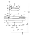
- the EL element has a basic structure of a 2-terminal type element, and a 3-terminal type EL element to which a third electrode is added is further disclosed.
- a 3-terminal type EL element to which a third electrode is added is further disclosed.
- an organic EL device in which an anode, a layer formed of an organic electroluminescence material called a light emitting material layer, a cathode, and an auxiliary electrode is provided for the cathode and the light emitting material layer via an insulating layer is disclosed. (See Patent Document 1).
- the light emitting transistor has a structure in which a hole injection layer, a carrier dispersion layer, a hole transport layer, and a light emitting layer are laminated from the anode side between the anode and the cathode, and an auxiliary electrode is provided for the anode via an insulating film.
- the light emitting transistor is disclosed (see Patent Document 2).
- an auxiliary electrode an insulating film provided on the auxiliary electrode, a first electrode provided on the insulating film having a predetermined size, a charge injection suppressing layer on the first electrode, and a first electrode are provided. It has a charge injection layer provided on an insulating film that is not provided, a charge injection suppression layer, a light emitting layer provided on the charge injection layer or the charge injection layer, and a second electrode provided on the light emitting layer.
- the organic light emitting transistor element configured as described above is disclosed (see Patent Documents 3 and 4).
- the organic EL device disclosed in Patent Document 1 Since the organic EL device disclosed in Patent Document 1 has low electron mobility in the light emitting material layer, the amount of electrons injected from the cathode is almost determined by the potential difference between the anode and the cathode, and is applied from the auxiliary electrode. There is a problem that the bias voltage has almost no effect on carrier injection. Since the light emitting material layer has low electron mobility and high resistance, the injection of electrons into the light emitting material layer is concentrated mainly in the vicinity of the cathode, and the bias voltage applied to the auxiliary electrode affects the injection amount of electrons. There is a problem that there is no.
- the light emitting transistor described in Patent Document 2 uses an external circuit to control the amount of carriers (electrons, holes) of different polarities injected into the light emitting layer in order to control the light emitting / non-light emitting state of the auxiliary electrode.
- carriers electrospray, holes
- the light emitting transistor described in Patent Document 1 has a problem that the position of a region where electrons and holes recombine in the light emitting layer, that is, a light emitting region cannot be controlled.
- the electron transport layer there is a problem that the thickness cannot be increased because the mobility is sufficiently large and there is no transparent material.
- the electron transport layer is formed by the sputtering method or the CVD method, it is costly to increase the size of the substrate, the process is complicated, and there is a problem in productivity. Further, these methods have a problem that processing at a high temperature is required.
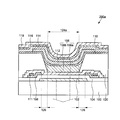
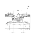
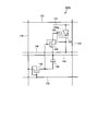
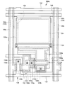
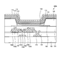
- the electroluminescence element includes a first electrode, a third electrode having a region facing the first electrode, and a first insulating layer between the first electrode and the third electrode.
- a second insulating layer between the first insulating layer and the third electrode, an electron transporting layer between the first insulating layer and the third electrode, and an electroluminescence material between the electron transporting layer and the third electrode. It has a light emitting layer including, and a second electrode arranged between the first insulating layer and the second insulating layer and electrically connected to the electron transport layer, and the second insulating layer has an opening.
- the opening has a superposed region in which the third electrode, the light emitting layer, the electron transport layer, the first insulating layer, and the first electrode overlap, and the second electrode is arranged outside the superposed region and is an electron transport layer.
- the second electron transport layer is in contact with the second electrode in the outer region of the opening, and the thickness of the end portion of the second electron transport layer is larger than that of the central portion of the opening.
- the display device includes a first electrode, a third electrode having a region facing the first electrode, a first insulating layer between the first electrode and the third electrode, and a first. Includes a second insulating layer between the insulating layer and the third electrode, an electron transporting layer between the first insulating layer and the third electrode, and an electroluminescence material between the electron transporting layer and the third electrode. It has a light emitting layer and a second electrode arranged between the first insulating layer and the second insulating layer and electrically connected to the electron transport layer, and the second insulating layer has an opening.
- the third electrode, the light emitting layer, the electron transport layer, the first insulating layer, and the first electrode have a superposed region on which the first electrode overlaps, the second electrode is arranged outside the superposed region, and the electron transport layer is arranged. It has a first electron transport layer in contact with the first insulating layer and a second electron transport layer arranged at the opening and in contact with the first electron transport layer, and the first electron transport layer is an opening of the second insulating layer.
- the second electron transport layer which is in contact with the second electrode in the outer region of the portion, has an electroluminescence element having a larger film thickness at the end than the center of the opening, and a drive transistor connected to the electroluminescence element.
- the electron transport layer by forming the electron transport layer with a coated oxide semiconductor, a dense and flat film having a sufficient thickness can be formed, and productivity is improved. can do.
- the electroluminescence device can control the amount of carrier injection into the light emitting layer by providing a third electrode that overlaps with the electron transport layer via the insulating layer.
- the electron transport layer of the electroluminescence device by forming the electron transport layer of the electroluminescence device with a coated oxide semiconductor, the transport characteristics of the carrier can be improved and uniform light emission can be obtained.
- the electroluminescence device can control the carrier balance between holes and electrons by providing an electrode for controlling the amount of carrier injected into the light emitting layer, thereby improving the luminous efficiency.
- the life time can be extended.
- a member or region is “above (or below)" another member or region, it is directly above (or directly below) the other member or region, unless otherwise specified. This includes not only certain cases but also cases above (or below) other members or areas. That is, it also includes the case where another component is included between the member or region above (or below) the other member or region.
- First Embodiment> 1. Structure of EL element The structure of the EL element is classified into a bottom emission type that emits light through the substrate and a top emission type that emits light on the opposite side of the substrate based on the light emission direction. Further, the structure of the EL element is laminated in the order of the anode, the hole transport layer, the light emitting layer, the electron transport layer, and the cathode from the substrate side, and vice versa, based on the stacking order in the manufacturing process. It is classified as a reverse stack structure. The EL element according to the present embodiment is classified into a reverse stacking structure, and can be applied to both a bottom emission type and a top emission type.
- FIG. 1 shows a cross-sectional structure of an EL element 200a according to an embodiment of the present invention.
- the EL element 200a shown in FIG. 1 is a bottom emission type and has a reverse stacking structure. That is, the EL element 200a has a first electrode 102, a first insulating layer 104, an electron transport layer 106 (first electron transport layer 106a, a second electron transport layer 106b), a light emitting layer 112, and a third electrode from the substrate 100 side. It has a structure in which 118 are laminated.
- FIG. 1 further shows a configuration in which a hole transport layer 114 and a hole injection layer 116 are arranged between the light emitting layer 112 and the third electrode 118.
- a hole transport layer 114 and a hole injection layer 116 are arranged between the light emitting layer 112 and the third electrode 118.
- one of the hole injection layer 116 and the hole transport layer 114 may be omitted, or may be replaced with a hole injection transport layer having both hole injection and hole transport functions. good.
- a hole block layer may be arranged between the electron injection layer 110 and the light emitting layer 112, or an electron block may be arranged between the light emitting layer 112 and the hole transport layer 114. Layers may be arranged.
- the EL element 200a shown in FIG. 1 includes a first electrode 102, a first insulating layer 104, an electron transport layer 106 (first electron transport layer 106a, second electron transport layer 106b), an electron injection layer 110, a light emitting layer 112, and a light emitting layer 112.
- the third electrode 118 is arranged so as to overlap in the vertical direction.
- the second electrode 108 is arranged outside the region where these layers overlap (superimposed region), and is arranged so as to be electrically connected to the first electron transport layer 106a. That is, the first electron transport layer 106a is provided wider than the first electrode 102. At least a part of the outer end of the first electron transport layer 106a is arranged outside the first electrode 102.
- the first electron transport layer 106a includes a region that overlaps with the first electrode 102 via the first insulating layer 104, and further includes a region that does not overlap with the first electrode 102 outside the region.
- the second electrode 108 is provided so as to be in contact with at least a part of the first electron transport layer 106a outside the superposed region.
- the second electrode 108 may be arranged so as to be sandwiched between the first electron transport layer 106a and the first insulating layer 104.
- the second electrode 108 is preferably provided so as to surround the outer periphery of the first electron transport layer 106a.
- the length from the central region of the first electron transport layer 106a to the second electrode 108 can be made uniform over the entire circumference.
- the EL element 200a according to the embodiment of the present invention is not limited to such an arrangement, and the second electrode 108 may be provided in a part of the peripheral portion of the first electron transport layer 106a. Just do it.
- the wiring 111 may be provided in a part of the region in contact with the second electrode 108. The wiring 111 may be arranged so as to be sandwiched between the second electrode 108 and the first electron transport layer 106a.
- the EL element 200a is provided with the upper surface of the second electrode 108 in contact with the first electron transport layer 106a, so that the contact area can be increased. As a result, the series resistance component of the EL element 200a is reduced and the drive voltage can be lowered. Further, the EL element 200a can reduce the current density flowing into the second electrode 108. Further, since the second electrode 108 is formed first, the EL element 200a can come into contact with the second electrode 108 in a region where the surface defects of the first electron transport layer 106a are small.
- the third electrode 118 has a function of injecting holes into the hole injection layer 116, and is an electrode also called an “anode” or an “anode”.
- the second electrode 108 has a function of injecting electrons into the electron transport layer 106, and is an electrode also called a “cathode” or a “cathode”.
- the first electrode 102 has a function of controlling the amount of carrier (electron) injected into the light emitting layer 112, and is also called a “carrier injection amount control electrode”.
- the electron transport layer 106 is represented by two distinct layers, a first electron transport layer 106a and a second electron transport layer 106b.
- the details of the electron transport layer 106 will be described later, but the first electron transport layer 106a and the second electron transport layer 106b have a common function of transporting electrons injected from the second electrode 108 to the light emitting layer 112.
- the electron concentration and electron mobility are different between the first electron transport layer 106a in contact with the second electrode 108 and the second electron transport layer 106b arranged on the side closer to the light emitting layer 112.
- the carrier concentration (electron concentration) of the second electron transport layer 106b may be relatively lower than the carrier concentration (electron concentration) of the first electron transport layer 106a in order to prevent the inactivation of excitons in the light emitting layer.
- the film thickness of the second electron transport layer 106b is thicker than the film thickness of the first electron transport layer 106a.
- the first electron transport layer 106a and the second electron transport layer 106b can also be regarded as one layer because of the common function of transporting the electrons injected from the second electrode 108 to the light emitting layer 112.
- the EL element 200a includes a second insulating layer 120 arranged between the first electron transport layer 106a and the electron injection layer 110.
- the second insulating layer 120 has an opening 124 that covers the peripheral edge of the first electron transport layer 106a and exposes the upper surface.
- the second electron transport layer 106b is arranged in the opening 124 of the second insulating layer 120.
- the area of the region where the second electron transport layer 106b is arranged is smaller than the area of the region where the first electron transport layer 106a is arranged.
- the first electron transport layer 106a and the second electron transport layer 106b come into contact with each other at the opening 124 of the second insulating layer 120.
- the first electron transport layer 106a, the second electron transport layer 106b, the electron injection layer 110, the light emitting layer 112, and the third electrode 118 are laminated.
- the region where these layers are laminated is the light emitting region of the EL element 200a.
- the light emitting region of the EL element 200a is defined by the opening 124 of the second insulating layer 120.
- the second electron transport layer 106b is arranged in the opening 124 of the second insulating layer 120.
- the film thickness of the second electron transport layer 106b is smaller than the film thickness of the second insulating layer 120. That is, the upper surface of the second electron transport layer 106b (the surface opposite to the substrate 100) is lower than the upper surface of the second insulating layer 120 (the surface opposite to the substrate 100) (the substrate 100 side).
- the second electron transport layer 106b has a concave shape in which the film thickness at the central portion is smaller than that at the end portion of the opening 124.
- the film thickness of the second electron transport layer 106b indicates the distance from the bottom of the opening 124 in the stacking direction (direction orthogonal to the upper surface of the substrate 100).
- the concave shape of the second electron transport layer 106b is arranged in the opening 124 of the second insulating layer 120.
- the concave surface shape of the upper surface of the second electron transport layer 106b is not particularly limited, but it is preferable that the concave surface shape is one continuous concave surface in the vicinity of the side wall of the second insulating layer 120 and is rounded.
- the upper surface of the second electron transport layer 106b has less uneven structure as compared with other film forming methods, and can form a flatter film.
- the film thickness of the second electron transport layer 106b needs to be 150 nm or more. It is preferable to form the film with a film thickness of 200 nm or more.
- the second electron transport layer 106b By configuring the second electron transport layer 106b in this way, the adhesive area between the second electron transport layer 106b and the second insulating layer 120 is increased, and the adhesion is improved. Further, since the second electron transport layer 106b has a film thickness larger than that of the central portion at the end portion, it is possible to suppress the concentration of the electric field at the end portions of the third electrode 118 and the second electrode 108, and it is resistant. It is possible to improve the voltage property, prevent the light emission from concentrating on the peripheral portion of the region 124a in which the opening 124 is arranged, and extend the light emission life of the element.
- the side surface of the second insulating layer 120 in the opening 124 is inclined so as to open upward. Due to the cross-sectional shape of the opening 124, the steepness of the step can be alleviated. As a result, when the light emitting layer 112, the third electrode 118, and the like are provided on the opening 124, each layer can be formed along the stepped portion. In other words, it is possible to prevent cracks from forming in the light emitting layer 112, the third electrode 118, and the like, resulting in so-called step breaks.
- the second electrode 108 is arranged so as to be sandwiched between the first insulating layer 104 and the second insulating layer 120.
- the second electrode 108 is arranged at a position not exposed from the opening 124 by being sandwiched between the first insulating layer 104 and the second insulating layer 120.
- the second electrode 108 is provided so as to overlap the third electrode 118 with the insulating layer interposed therebetween. Since the end portion of the second electrode 108 is not exposed to the opening 124 of the second insulating layer 120, the electric field concentration is not generated between the third electrode 118 and the second electrode 108 in the light emitting region.
- the second electrode 108 is sandwiched between the first insulating layer 104 and the second insulating layer 120, and the end portion of the second electrode 108 is an opening of the second insulating layer 120.
- the portion 124 outside the region 124a in which the portion 124 is arranged, the withstand voltage of the EL element 200a is increased, and the uniformity of the emission intensity in the light emitting region is enhanced.
- the second insulating layer 120 By providing the second insulating layer 120, the distance between the third electrode 118 and the second electrode 108 can be widened, and the parasitic capacitance can be reduced.
- the first electron transport layer 106a is affected by the electric field formed by the first electrode 102.
- the amount of carriers (electrons) transported from the electron transport layer 106 (first electron transport layer 106a, second electron transport layer 106b) to the light emitting layer 112 can be controlled by the electric field strength of the first electrode 102. .. As the voltage applied to the first electrode 102 increases, the electric field acting on the electron transport layer 106 (first electron transport layer 106a, second electron transport layer 106b) also increases.
- the electric field generated by applying a positive voltage to the first electrode 102 acts to attract carriers (electrons) from the second electrode 108 to the first electron transport layer 106a, and is therefore transported to the light emitting layer 112. It is possible to increase the amount of carriers (electrons).
- the first electrode 102 is preferably arranged so as to overlap the offset region 126 of the first electron transport layer 106a. With such an arrangement, the first electrode 102 can apply an electric field to the offset region 126.
- carriers electrospray
- the offset region 126 When a positive voltage is applied to the first electrode 102, carriers (electrons) are induced in the first electron transport layer 106a forming the offset region 126, and it is possible to prevent the offset region 126 from increasing in resistance.
- the length of the offset region 126 is about 2 ⁇ m to 10 ⁇ m, it is possible to prevent electrons from flowing from the second electrode 108 to the first electron transport layer 106a when the first electrode 102 is connected to the ground potential. .. That is, the offset region 126 operates as a thin film transistor (TFT) having the first electrode 102 as the bottom gate.
- TFT thin film transistor
- the first electrode 102 has translucency.
- the first electrode 102 is formed of a transparent conductive film.
- the third electrode 118 has a light reflecting surface for reflecting the light emitted from the light emitting layer 112.
- the third electrode 118 is preferably formed of a material having a large work function in order to inject holes into the hole injection layer 116.
- the third electrode 118 is formed of a transparent conductive film such as indium tin oxide (ITO).
- ITO indium tin oxide
- the light reflecting surface of the third electrode 118 can be formed, for example, by laminating a metal film such as an aluminum alloy on a transparent conductive film.
- the electron transport layer 106 (first electron transport layer 106a, second electron transport layer 106b) is formed of a translucent oxide semiconductor.
- Oxide semiconductors having translucency are inorganic materials and are thermally stable because they are oxides.
- the EL element 200a can realize stable light emission without deterioration of characteristics even if it has a reverse stacking structure.
- FIG. 2 shows a top-emission type EL element 200b.
- the top emission type EL element 200b has the same structure as the bottom emission type EL element 200a shown in FIG. 1, except that the configurations of the third electrode 118 and the first electrode 102 are different.
- the first electrode 102 is formed of a metal film so that a light reflecting surface is formed, and the third electrode 118 is such that light emitted from the light emitting layer 112 is transmitted. It is formed of a transparent conductive film. Since the second electrode 108 is arranged outside the light emitting region, it is not necessary to change the structure and constituent materials in particular.
- the upper layer of the third electrode 118 typically a plasma CVD as a thin film encapsulation layer (Chemical Vapor Deposition) method or produced silicon nitride film by a sputtering method (Si 3 N 4 film), a silicon oxide film (SiO 2 film) , Aluminum oxide film (Al 2 O 3 film), etc. are formed, but are omitted in this figure.
- a plasma CVD as a thin film encapsulation layer (Chemical Vapor Deposition) method or produced silicon nitride film by a sputtering method (Si 3 N 4 film), a silicon oxide film (SiO 2 film) , Aluminum oxide film (Al 2 O 3 film), etc.
- the top emission type EL element 200b differs from the bottom emission type EL element 200a only in the configurations of the third electrode 118 and the first electrode 102. That is, the EL element according to the present embodiment can realize both a bottom emission type and a top emission type with a slight change while having a common reverse stacking type structure.
- the electron transport layer 106, the electron injection layer 110, the light emitting layer 112, and the third electrode 118 are laminated at least in the vertical direction.
- the first electrode 102 is provided so as to be close to the electron transport layer 106 with the first insulating layer 104 interposed therebetween, and the second electrode 108 is arranged in the outer peripheral region of the region 124a in which the opening 124 is arranged.
- the amount of carriers (electrons) transported from the electron transport layer 106 to the light emitting layer 112 by controlling the potential of the first electrode 102 independently of the third electrode 118 and the second electrode 108. Can be controlled.
- the EL element 200 makes it possible to realize both a bottom emission type structure and a top emission type structure by appropriately selecting the materials of the first electrode 102 and the third electrode 118.
- the first electrode 102 is formed by using a metal material, a conductive metal oxide material, a metal nitride material, or a metal oxynitride material.
- the metal material is formed of a metal material such as aluminum (Al), silver (Ag), titanium (Ti), molybdenum (Mo), tantalum (Ta), an alloy material using these metals, or a laminated metal. ..
- the metal oxide material examples include indium tin oxide (In 2 O 3 ⁇ SnO 2 : ITO), indium zinc oxide (In 2 O 3 ⁇ ZnO: IZO), tin oxide (SnO 2 ), and zinc oxide (ZnO). Can be used. Further, as the metal oxide material, titanium oxide (TiO x : Nb) doped with niobium (Nb) or the like can be used. As the metal nitride material, titanium nitride (TiN x ), zirconium nitride (ZrN x ) or the like can be used.
- the metal oxynitride materials titanium oxynitride (TiO x N y), tantalum oxynitride (TaO x N y), zirconium oxynitride (ZrO x N y), using such hafnium oxynitride (HfO x N y) be able to.
- a trace amount of metal element that improves conductivity may be added to these metal oxide materials, metal nitride materials, and metal oxynitride materials.
- titanium oxide (TIM x : Ta) doped with tantalum (Ta) may be used.
- the material forming the first electrode 102 is appropriately selected depending on whether the EL element 200 is a top emission type or a bottom emission type.
- the first electrode 102 is formed of a metal oxide material, a metal nitride material or a metal oxynitride material having conductivity and translucency.
- the EL element 200a can transmit the light emitted by the light emitting layer 112 through the first electrode 102 and emit it.
- the first electrode 102 is made of a metal material having a high reflectance with respect to visible light. Since the first electrode 102 is made of a metal material, the EL element 200b can reflect the light emitted by the light emitting layer 112 and emit it from the third electrode 118.
- the first insulating layer 104 is formed by using an inorganic insulating material.
- an inorganic insulating material silicon oxide, silicon nitride, silicon oxynitride, aluminum oxide and the like can be selected.
- the first insulating layer 104 is formed by using a plasma CVD (Chemical Vapor Deposition) method, a sputtering method, or the like.
- the first insulating layer 104 is formed with a film thickness of 50 nm to 900 nm, preferably 100 nm to 600 nm.
- the electric field generated by the first electrode 102 can act on the electron transport layer 106, and even when the bias voltage is increased, the first is due to the tunnel effect. It is possible to prevent the tunnel current from flowing from the electrode 102 to the electron transport layer 106.
- the first insulating layer 104 can have both insulating properties and transparency. Thereby, it can be applied to both the bottom emission type EL element 200a and the top emission type EL element 200b. Further, it is possible to insulate between the first electrode 102 and the electron transport layer 106, and between the first electrode 102 and the second electrode 108.
- the second insulating layer 120 is formed of a polar organic insulating material.
- a linear fluoroorganic material may be used.
- a fluoroalkylsilane (FAS) -based material is used.
- the fluoroalkylsilane (FAS) -based material include H, 1H, 2H, 2H-perfluorodecyltrichlorosilane (FDTS), tridecafluoro-1,1,2,2-tetrahydrooctyltrichlorosilane (FOTS) and the like. Used.
- the second insulating layer 120 may contain, for example, a fluorine-based liquid repellent in the photosensitive resin material.
- a fluorine-based liquid repellent in the photosensitive resin material.
- Positive-type photosensitive resin compositions and negative-type photosensitive resin compositions mainly composed of linear fluorine-based organic materials are already on the market, and an appropriate amount of a fluorine-based liquid repellent is mixed with these photosensitive resin compositions to repel them. It is possible to adjust the liquid performance.
- the second insulating layer 120 is formed by using a linear fluorine organic material, so that a surface having poor wettability and high liquid repellency is formed. In other words, by forming the second insulating layer 120 containing bipolar molecules and side chains, a negative charge appears on the upper surface of the second insulating layer 120 due to the microphase separation phenomenon. As will be described later, the second insulating layer 120 is formed with an opening 124 for exposing the first electron transport layer 106a, and then the second electron transport layer 106b is formed in the opening 124 of the second insulating layer 120. ..
- the side surface of the second insulating layer 120 in the opening 124 is highly wettable and highly liquid-friendly. By utilizing the liquid repellency of the upper surface of the second insulating layer 120 and the liquid repellency of the side surface of the opening, the second electron transport layer 106b can be efficiently arranged in the opening 124 of the second insulating layer 120.
- an organic insulating material such as polyimide, acrylic, or epoxy may be used for the second insulating layer 120.
- the upper surface of the second insulating layer 120 may be improved in liquid repellency by, for example, fluorine-based plasma treatment.
- the opening 124 of the second insulating layer 120 is preferably inclined in a tapered shape, but the cross-sectional shape of the opening 124 can be formed in a tapered shape by using a photosensitive organic insulating material.
- the film thickness of the second insulating layer 120 is not particularly limited, but may be formed, for example, with a thickness of 200 nm to 5000 nm. When the second insulating layer 120 has a function as a flattening film, the film thickness may be increased to about 2 ⁇ m to 5 ⁇ m.
- Electron transport layer The electron transport layer 106 may be formed of a material having high electron mobility in order to transport carriers (electrons) injected from the second electrode 108 into the plane of the light emitting region of the EL element 200. preferable. Further, in the case of the bottom emission type, the electron transport layer 106 is arranged on the light emitting side with respect to the light emitting layer, so that it is preferably formed of a material having good visible light translucency. Further, in order to make the carrier concentration different between the first electron transport layer 106a and the second electron transport layer 106b, it is preferable that the carrier concentration is made of a material that can be easily controlled.
- a metal oxide material is used for the electron transport layer 106 (first electron transport layer 106a, second electron transport layer 106b).
- the metal oxide material it is preferable to use an oxide semiconductor material having a band gap of 2.8 eV or more, preferably 3.0 eV or more, and having high electron mobility.
- Such an oxide semiconductor material has semiconductor characteristics even when a thin film is formed, is transparent to visible light, and has n-type electrical conductivity.
- oxide semiconductor material applied to the electron transport layer 106 examples include a quaternary oxide material, a ternary oxide material, a binary oxide material, and a single oxide material.
- the metal oxide material exemplified here is classified as an oxide semiconductor because it has a bandgap of 2.8 eV or more, exhibits n-type conductivity, and can control the donor concentration by oxygen deficiency or the like. ..
- quaternary oxide material In 2 O 3 -Ga 2 O 3 -SnO 2 -ZnO -based oxide material, a ternary oxide material as In 2 O 3 -Ga 2 O 3 -ZnO -based oxide material, In 2 O 3 -SnO 2 -ZnO-based oxide material, In 2 O 3 -Ga 2 O 3 -SnO 2 based oxide material, In 2 O 3 -Ga 2 O 3 -SmO x based oxide material, an In 2 O 3 -Al 2 O 3 -ZnO-based oxide materials, Ga 2 O 3 -SnO 2 -ZnO-based oxide materials, Ga 2 O 3 -Al 2 O 3 -ZnO -based oxide materials, SnO 2 -Al 2 O 3- ZnO-based oxide material, In 2 O 3- ZnO-based oxide material as binary oxide material, In 2 O 3- Ga 2 O 3- based oxide material, In 2 O 3- WO 3- based oxide material,
- the metal oxide material may contain silicon (Si), nickel (Ni), tungsten (W), hafnium (Hf), titanium (Ti), zirconium (Zr), and tantalum (Ta).
- the In—Ga—Zn—O-based oxide material shown above is a metal oxide material containing at least In, Ga, and Zn, and the composition ratio thereof is not particularly limited.
- a material represented by the chemical formula InMO 3 (ZnO) m (m> 0) can be used for the first electron transport layer 106a and the second electron transport layer 106b.
- M represents one or more metal elements selected from Ga, Al, Mg, Ti, Ta, W, Hf and Si.
- the above-mentioned quaternary oxide material, ternary oxide material, binary oxide material, and unidimensional oxide material are not limited to those having a stoichiometric composition in the oxide contained in the chemical. It may be composed of an oxide material having a composition deviating from the stoichiometric composition. Further, the oxide semiconductor layer as the electron transport layer 106 may have an amorphous phase, may have crystallinity, or may be a mixture of an amorphous phase and a crystalline phase.
- the first electron transport layer 106a and the second electron transport layer 106b are preferably formed of oxide semiconductor materials having different compositions.
- the first electron transport layer 106a is formed of a tin (Sn) -based oxide semiconductor (InGaSnO x , InWSnO x , InAlSnO x , InSiSnO x ) that can obtain high electron mobility and high PBTS reliability evaluation. Is preferable.
- the second electron transport layer 106b is less likely to large size crystallized, amorphous film or nanocrystallites film easily form zinc (Zn) based oxide semiconductor (ZnSiO x of, ZnMgO x, ZnAlO x, ZnIn , ZnGaO x etc. ) Is preferable.
- the first electron transport layer 106a is a metal oxide containing tin oxide as a main component and at least one selected from gallium oxide, tungsten oxide, aluminum oxide and silicon oxide.
- the second electron transport layer 106b is preferably a metal oxide containing zinc oxide as a main component and at least one selected from silicon oxide, magnesium oxide, indium oxide, aluminum oxide and gallium oxide.
- the band gaps of the first electron transport layer 106a and the second electron transport layer 106b can be optimized.
- the band gap of the second electron transport layer 106b can be made larger than the band gap of the first electron transport layer 106a.
- the band gap of the first electron transport layer 106a can be set to 3.0 eV or more
- the band gap of the second electron transport layer 106b can be set to be equal to or larger than the bad gap of the first electron transport layer 106a.
- the band gap of the second electron transport layer 106b is preferably 3.4 eV or more.
- the electron transport layer 106 (first electron transport layer 106a, second electron transport layer 106b), indium tin oxide (In 2 O 3 ⁇ SnO 2 : ITO) and indium zinc oxide (In 2 O 3 ⁇ ZnO: IZO) ), Tin oxide (SnO 2 ), titanium oxide (TIM x ) and the like are used.
- the metal nitride material gallium nitride (GaN), aluminum nitride gallium (GaAlN x ), or the like is used.
- the metal oxynitride materials titanium oxynitride (TiO x N y), tantalum oxynitride (TaO x N y), zirconium oxynitride (ZrO x N y), hafnium oxynitride (HfO x N y) or the like is used Be done.
- a trace amount of metal element that improves conductivity may be added to these metal oxide materials, metal nitride materials, and metal oxynitride materials.
- niobium-doped titanium oxide (TiO x : Nb) may be used.
- the oxygen content or the nitrogen content may be adjusted.
- the first electron transport layer 106a formed of the oxide semiconductor material can be formed by a sputtering method, a vacuum vapor deposition method, a coating method, or the like.
- the second electron transport layer 106b formed of the oxide semiconductor material can be formed by a coating method.
- the first electron transport layer 106a preferably has a film thickness of 10 nm to 70 nm, and the second electron transport layer 106b is preferably formed with a film thickness of 150 nm to 900 nm.
- the second electron transport layer 106b should be as thick as possible.
- the electron mobility of the second electron transport layer 106b is preferably 1/10 or less of the electron mobility of the first electron transport layer 106a.
- the electron mobility of the first electron transport layer 106a is preferably 10 cm 2 / V ⁇ sec to 200 cm 2 / V ⁇ sec
- the electron mobility of the second electron transport layer 106b is 0.001 cm 2 / V ⁇ . It is preferably sec to 10 cm 2 / V ⁇ sec.
- the first electron transport layer 106a has a high carrier concentration and high electron mobility as described above, it is possible to reduce the resistance in a short time when a positive voltage is applied to the first electrode 102. can.
- the first electron transport layer 106a can make the in-plane distribution of electrons injected from the second electrode 108 uniform.
- the second electrode 108 can transport the carriers (electrons) injected from the peripheral portion of the first electron transport layer 106a toward the center to make the electron concentration in the light emitting region uniform. ..
- the emission intensity of the EL element 200 can be made uniform in the plane.
- the carriers (electrons) injected from the second electrode 108 can be transported to the region where the electric field of the first electrode 102 acts in a short time. can.
- the second electron transport layer 106b is arranged in close proximity to the light emitting layer 112. Therefore, if the carrier concentration (electron concentration) of the second electron transport layer 106b is 10 20 / cm 3 or more, the excited state in the light emitting layer 112 is deactivated and the luminous efficiency is lowered. On the other hand, when the carrier concentration (electron concentration) of the second electron transport layer 106b is 10 11 / cm 3 or less, the carriers supplied to the light emitting layer 112 decrease and sufficient brightness cannot be obtained.
- the current flowing through the second electron transport layer 106b needs to be a space charge limiting current in order to obtain uniform emission intensity.
- 2nd electrode cathode
- a material such as an aluminum-lithium alloy (AlLi) or a magnesium-silver alloy (MgAg) has been used.
- AlLi aluminum-lithium alloy
- MgAg magnesium-silver alloy
- these materials are easily deteriorated by the influence of oxygen and moisture in the atmosphere and are difficult to handle.
- these materials are metals or alkali metals, and in order to have translucency, they need to be thinned to form a semi-transmissive film.
- the sheet resistance increases when the cathode is thinned.
- the resistance of the electrode acts as a series resistance component in the EL element, thinning the cathode becomes a factor of increasing the driving voltage and increasing the power consumption. Further, it also causes non-uniformity of emission intensity (luminance) in the plane of the emission region of the EL element.
- the EL element 200 is formed of a metal oxide material, a metal nitride material, or a metal oxynitride material in which the second electrode 108 has conductivity.
- the second electrode 108 is formed by a low resistance oxide conductor film.
- the metal oxide conductor material include tin oxide (In 2 O 3 ⁇ SnO 2 : ITO), tin oxide zinc oxide (In 2 O 3 ⁇ SnO 2 ⁇ ZnO: ITZO), and tin oxide silicon (In).
- titanium oxide (TIO x : Nb) doped with niobium (Nb) or the like can be applied to the second electrode 108, and as the metal nitride material, titanium nitride (TiN x) can be applied.
- zirconium nitride (ZrN x), etc. as the metal oxynitride materials, titanium nitride (TiO x N y), tantalum oxynitride (TaO x N y), zirconium oxynitride (ZrO x N y ), hafnium oxynitride (HfO x N y ) and the like can be applied. Further, a trace amount of metal element that improves conductivity may be added to these metal oxide materials, metal nitride materials, and metal oxynitride materials. For example, tantalum-doped titanium oxide (TIM x : Ta) may be used.
- a refractory metal silicide oxide such as TiSiO x may be used.
- a metal oxide material, a metal nitride material, and a metal oxynitride material exhibiting n-type electrical conductivity it is possible to ensure the stability of the bonding even when the material is brought into contact with the wiring 111. That is, by using such a metal oxide material, a metal nitride material, and a metal oxynitride material, it is possible to prevent a redox reaction (local battery reaction) with aluminum (Al) having a low potential. Can be done.
- the carrier concentration of the second electrode 108 is preferably 10 20 / cm 3 to 10 21 / cm 3. By having such a carrier concentration, the second electrode 108 can reduce the resistance and suppress the series resistance loss. As a result, the power consumption of the EL element 200 can be reduced and the current efficiency can be increased.
- Electron Injection Layer In EL devices, the electron injection layer is used to reduce the energy barrier for injecting electrons from the cathode into the electron transport material.
- the EL element 200 according to the present embodiment is preferably provided with an electron injection layer 110 in order to facilitate the injection of electrons from the electron transport layer 106 formed of the oxide semiconductor into the light emitting layer 112.
- the electron injection layer 110 is provided between the electron transport layer 106 and the light emitting layer 112. As shown in FIGS. 1 and 2, it is important that the electron injection layer 110 is formed on the entire display area in order to improve the yield and reliability.
- the electron injection layer 110 be formed using a material having a small work function in order to inject electrons into the light emitting layer 112 formed containing the electroluminescence material.
- the electron injection layer 110 is composed of a calcium (Ca) oxide and an aluminum (Al) oxide.
- the electron injection layer 110 for example, preferably used C12A7 (12CaO ⁇ 7Al 2 O 3 ) electride.
- C12A7 electride has semiconductor characteristics, can be controlled from high resistance to low resistance, and has a work function of 2.4 eV to 3.2 eV, which is about the same as that of alkali metals, and is therefore suitable as an electron injection layer 110. Can be used for.
- the electron injection layer 110 by C12A7 electride is produced by a sputtering method targeting a polycrystal of C12A7 electride. Since the C12A7 electride has semiconductor characteristics, the film thickness of the electron injection layer 110 can be in the range of 1 nm to 10 nm.
- the C12A7 electride preferably has a Ca: Al molar ratio in the range of 13:13 to 11:16.
- the electron injection layer 110 using the C12A7 electride can be formed by using a sputtering method.
- the electron injection layer 110 formed of the C12A7 electride is preferably amorphous, but may have crystallinity.
- C12A7 electride is stable in the atmosphere, lithium fluoride (LiF), lithium oxide (Li 2 O), sodium chloride (NaCl), potassium chloride (KCl), etc., which have been conventionally used as electron injection layers, etc. It has the advantage of being easier to handle than the alkali metal compounds of. As a result, in the manufacturing process of the EL element 200, it is not necessary to work in dry air or an inert gas, and the limitation of manufacturing conditions is relaxed.
- the C12A7 electride since the C12A7 electride has a large ionization potential, it can be used as a hole block layer by arranging it on the opposite side of the hole transport layer 114 with the light emitting layer 112 interposed therebetween. That is, by providing the electron injection layer 110 formed of C12A7 electride between the electron transport layer 106 and the light emitting layer 112, the holes injected into the light emitting layer 112 penetrate to the second electrode 108 side. It can be suppressed and the luminous efficiency can be increased.
- Zn 0.7 Mg 0.3 O x and Zn 0.75 Si 0.25 O x and a 1: 4 to 1: can be used as the electron injecting layer be three-component metal oxide semiconductor material mixed in the range of 10 .. If the electron injection layer is to be the specific resistance value of more than 10 7 ⁇ ⁇ cm when the thickness of 10nm by adjusting the oxygen partial pressure of the mixed gas of Ar and O 2 so deposited by sputtering method , Cross talk with the adjacent pixel can be prevented.
- Light-emitting layer 112 is formed using an electroluminescence material.
- an electroluminescence material for example, a fluorescent compound material that emits fluorescence, a phosphorescent compound material that emits phosphorescence, or a thermally activated delayed fluorescence (TADF) can be used.
- TADF thermally activated delayed fluorescence
- N, N'-bis [4- (9H-carbazole-9-yl) phenyl] -N, N'-diphenylstilbene-4,4'-diamine (YGA2S), 4- (9H-carbazole-9-yl) -4'-(10-phenyl-9-anthryl) triphenylamine (YGAPA) and the like can be used.
- the green light emitting material include N- (9,10-diphenyl-2-anthryl) -N, 9-diphenyl-9H-carbazole-3-amine (2PCAPA) and N- [9,10-bis (1,10-bis).
- red light emitting material examples include N, N, N', N'-tetrakis (4-methylphenyl) tetracene-5,11-diamine (pmPhTD), 7,13-diphenyl-N, N, N'. , N'-Tetrakis (4-methylphenyl) acenaft [1,2-a] fluoranthene-3,10-diamine (pmPhAFD) and the like can be used.
- phosphorescent materials such as bis [2- (2'-benzo [4,5- ⁇ ] thienyl) pyridinato N, C3 ' ] iridium (III) acetylacetonate (Ir (btp) 2 (acac)) are used. be able to.
- the light emitting layer 112 various known materials such as quantum dots (QD), perovskite-based inorganic light-emitting materials, and perovskite-based inorganic-organic hybrid light-emitting materials can be used.
- the light emitting layer 112 can be produced by a vapor deposition method, a transfer method, a spin coating method, a spray coating method, a printing method (inkjet printing method, gravure printing method) or the like.
- the film thickness of the light emitting layer 112 may be appropriately selected, and is provided in the range of, for example, 10 nm to 100 nm.
- FIGS. 1 and 2 show an example in which the light emitting layer 112 is separated for each EL element, when a plurality of EL elements are arranged on the same plane, the light emitting layer 112 extends over the plurality of light emitting elements. It may be provided so as to be continuous. An electron blocking layer may be formed on the entire surface between the light emitting layer 112 and the hole transporting layer 114, but this is omitted in FIGS. 1 and 2.
- the hole transport layer 114 is formed by using a material having a hole transport property.
- the hole transport layer 114 may be, for example, an arylamine compound, an amine compound containing a carbazole group, an amine compound containing a fluorene derivative, or the like.
- the hole transport layer 114 is, for example, 4,4'-bis [N- (naphthyl) -N-phenyl-amino] biphenyl ( ⁇ -NPD), N, N'-bis (3-methylphenyl)-(1).
- the hole transport layer 114 is manufactured by a general film forming method such as a vacuum vapor deposition method or a coating method.
- the hole transport layer 114 is made with a film thickness of 10 nm to 500 nm.
- the hole injection layer 116 contains a substance having a high hole injection property with respect to the organic layer.
- a metal oxide such as molybdenum oxide, vanadium oxide, ruthenium oxide, tungsten oxide, and manganese oxide can be used.
- Such a hole injection layer 116 is manufactured by a general film forming method such as a vacuum vapor deposition method or a coating method.
- the hole injection layer 116 is manufactured with a film thickness of 1 nm to 100 nm.
- the third electrode 118 is made of a metal, an alloy, or a conductive compound having a large work function (specifically, 4.0 eV or more).
- a metal, an alloy, or a conductive compound having a large work function specifically, 4.0 eV or more.
- ITO indium tin oxide
- IZO indium zinc oxide
- IWZO indium oxide containing tungsten oxide and zinc oxide
- the third electrode 118 in which these conductive metal oxide materials are used is manufactured by a vacuum vapor deposition method or a sputtering method.
- the third electrode 118 is located on the back surface of the emission surface, it is preferable to have a light reflection surface. In this case, it is preferable that the third electrode 118 has a metal film laminated on the transparent conductive film.
- the third electrode 118 can be formed by using the transparent conductive film as described above.
- Wiring For the wiring 111, a metal material having high conductivity such as aluminum (Al) and copper (Cu) is used.
- the wiring 111 is made of an aluminum alloy, a copper alloy, or a silver alloy.
- Aluminum alloys include aluminum-neodium alloy (Al-Nd), aluminum-titanium alloy (Al-Ti), aluminum-silicon alloy (Al-Si), aluminum-neodium-nickel alloy (Al-Nd-Ni), and aluminum.
- -Carbon-nickel alloy (Al-C-Ni), copper-nickel alloy (Cu-Ni) and the like can be applied. By using such a metal material, it is possible to have heat resistance and reduce wiring resistance.
- electrodes having a three-layer laminated structure such as Mo / Al / Mo and Mo / Cu / Mo are also effective. That is, a three-layer laminated structure in which the above-mentioned metal material is sandwiched between molybdenum (Mo), zirconium (Zr), titanium (Ti), or an antioxidant layer containing an alloy material thereof can also be applied.
- FIG. 3 schematically shows the configuration of the EL element 200 according to the present embodiment.
- FIG. 3 shows the second electrode 108, the electron transport layer 106, the electron injection layer 110, the light emitting layer 112, the hole transport layer 114, the hole injection layer 116, the third electrode 118, and the third electrode as members constituting the EL element 200.
- the structure in which the insulating layer 104 and the first electrode 102 are provided is shown.
- the EL element 200 is a kind of light emitting diode, and emits light by passing a forward current between the third electrode (anode) 118 and the second electrode (cathode) 108.
- the third power supply 128c is connected between the third electrode 118 and the ground (earth)
- the second power supply 128b is connected between the second electrode 108 and the ground (earth)
- the first electrode 102 is shown.
- the second switch 130b is connected in series between the first power source 128a and the first power supply 128a
- the first switch 130a is connected between the first electrode 102 and the ground (earth).
- FIG. 3 shows a state in which the first switch 130a and the second switch 130b are off in the switch 130, and no bias is applied to the first electrode 102.
- the electron transport layer 106 and the third electrode 118 are arranged to face each other on the first insulating layer 104 with the light emitting layer 112 interposed therebetween, and the second electrode 108 is connected at the peripheral edge of the first electron transport layer 106a.
- the light emitting region the region where the electron transport layer 106, the electron injection layer 110, the light emitting layer 112, and the third electrode 118 are superimposed
- the electric field distribution generated between the third electrode 118 and the second electrode 108 is not uniform in the light emitting region, and the electric field is concentrated at the ends of the second insulating layer 120 and the second electrode 108.
- the carriers (electrons) injected from the second electrode 108 are not uniformly distributed in the plane of the first electron transport layer 106a, and the first is 2 Injected into the end of the electron transport layer 106b. Since the film thickness at the end of the second electron transport layer 106b according to the present embodiment is larger than the film thickness at the center, the electric field concentration at the end of the second electron transport layer 106b is relaxed. Therefore, the offset region 126 can be shortened, and the area of the light emitting region can be increased accordingly.
- FIG. 4 shows a state in which the first switch 130a is turned on and the potential of the first electrode 102 is the ground potential in the switch 130.
- this state there are no carriers (electrons) in the first electron transport layer 106a, and the first electron transport layer 106a is in an insulated state.
- no current flows through the EL element 200, and the EL element 200 is in a non-light emitting state (non-light emitting state).
- the first electrode 102 operates as a bottom gate, so that the first electron transport layer 106a in the offset region 126 becomes a depletion layer and no current flows.
- the electric field formed by the first electrode 102 is formed. Acts on the first electron transport layer 106a. Since a positive voltage is applied to the first electrode 102, the carriers (electrons) injected from the second electrode 108 into the first electron transport layer 106a are drifted to the central region of the first electron transport layer 106a. Thereby, the carriers (electrons) are transported from the peripheral portion of the first electron transport layer 106a to the central region of the first electron transport layer 106a. The electric field generated by the first electrode 102 to which a positive voltage is applied acts to spread the carriers (electrons) injected from the second electrode 108 over the entire in-plane of the first electron transport layer 106a.
- the carriers (electrons) transported to the central region of the first electron transport layer 106a move from the first electron transport layer 106a toward the light emitting layer 112.
- the carriers (holes) injected from the third electrode 118 and the carriers (electrons) injected from the second electrode 108 are recombined in the light emitting layer 112 to generate excitons, and the excitons in the excited state are generated. Photons are emitted and observed as light emission when the state transitions to the ground state.
- the amount of carriers (electrons) injected into the first electron transport layer 106a can be controlled by the voltage of the second electrode 108.
- the amount of carrier (electron) injected into the first electron transport layer 106a can be increased.
- the amount of carriers (electrons) injected from the first electron transport layer 106a into the light emitting layer 112 can be controlled by the voltage of the first electrode 102.
- a large amount of carriers (electrons) injected from the second electrode 108 are drawn into the central region of the first electron transport layer 106a, and the amount of carrier injection into the light emitting layer 112 is increased. be able to.
- the second electron transport layer 106b according to the present embodiment has a larger film thickness at the end portion than at the center portion. Therefore, it is possible to suppress the concentration of the electric field at the end of the second electron transport layer 106b, and it is possible to improve the withstand voltage. Further, in order to suppress leakage from the side wall of the second electron transport layer 106b and improve reliability, the third insulating layer 122 may be laminated on the lower layer of the second insulating layer 120 as shown in FIG.
- the conventional EL element has a problem that the carrier balance is lost and the luminous efficiency is lowered because the electron mobility is lower than the hole mobility of the light emitting layer. Further, in the EL element, when the carrier balance is lost and the number of holes in the light emitting layer becomes excessive, holes are accumulated at the interface between the light emitting layer and the electron transport layer, which accelerates the deterioration of current efficiency (luminous efficiency). It has the problem of becoming a factor. Therefore, attempts have been made to balance the holes and electrons injected into the light emitting layer by adjusting the material and film thickness of the hole transport layer and the electron transport layer. However, even if the element structure of the EL element itself is adjusted, there is a problem that it cannot follow the time-dependent change and the temperature change of the light emission characteristics.
- the EL element 200 can control the carrier balance by the first electrode 102. That is, the carrier balance can be controlled by controlling the amount of carriers (electrons) transported to the light emitting layer 112 by the first electrode 102 provided on the electron transport layer 106 side. That is, the electrons are transferred by the first electrode 102 so that the amount of electrons transported from the second electrode 108 to the light emitting layer 112 is not insufficient with respect to the amount of holes transported from the third electrode 118 to the light emitting layer 112. By increasing the transport amount, it is possible to control the number of holes and electrons in the light emitting layer 112 to be the same.
- the carrier balance can be controlled by controlling the amount of carriers (electrons) transported to the light emitting layer 112 by the first electrode 102 provided on the electron transport layer 106 side. That is, the electrons are transferred by the first electrode 102 so that the amount of electrons transported from the second electrode 108 to the light emitting layer 112 is not insufficient with respect to the amount of holes transported from the third electrode 118 to
- the EL element 200 is injected from the electron injection layer 110 into the light emitting layer 112 with respect to the hole current injected from the hole transport layer 114 into the light emitting layer 112 as shown in FIG. 32.
- the carriers (electrons) injected into the electron transport layer 106 from the second electrode 108 become an electron current (Ie) and become a light emitting layer from the first electron transport layer 106a. It flows toward 112. At this time, the electron current (Ie) increases exponentially like the forward current of the diode (“I region” shown in FIG. 6).
- a change in electron current (Ie) means an increase or decrease in the amount of holes and electrons injected into the light emitting layer 112.
- the EL element 200 can control the position of the light emitting region in the light emitting layer 112 in the thickness direction by the voltage of the first electrode 102.
- the voltage of the first electrode 102 is changed between the first voltage (Vg1) and the second voltage (Vg2), the position of the light emitting region in the light emitting layer 112 is shaken between the cathode side A and the anode side B. Can be moved.
- the entire light emitting layer 112 can be used as a light emitting region.
- the lifetime of the luminance deterioration (for example, the time when the initial luminance is reduced to 70%) can be extended.
- the voltage of the first electrode 102 is made to fluctuate between Vg1 and Vg2 shown in FIG. 6, and the intensity of luminance can be controlled by the potential difference (voltage) between the second electrode 108 and the third electrode 118. ..
- the electron transport layer is formed by the oxide semiconductor layer, and the first electrode for controlling the carrier injection amount is arranged with the insulating layer sandwiched between the electron transport layers.
- the first electrode facing the third electrode 118 which is an anode, the amount of electrons injected into the light emitting layer can be controlled.
- the EL device according to the present embodiment can control the carrier balance of electrons and holes in the light emitting layer by the action of the first electrode that controls the carrier injection amount. As a result, the current efficiency of the EL element can be increased and the life time can be extended.
- the entire thickness direction of the light emitting layer is not uniformly deteriorated, and the light emitting layer is unevenly deteriorated, so that it is difficult to suppress the luminance deterioration and the life time of the EL element is extended. I wouldn't.
- the entire light emitting layer 112 can be set as a light emitting region by controlling the voltage of the first electrode 102, whereby the thickness direction of the light emitting layer 112 can be set. Since the whole can be uniformly deteriorated, it is possible to extend the life time for the deterioration of brightness.
- the rectangular staircase wave or trapezoidal staircase wave of FIG. 33 is preferable as the voltage waveform.
- FIG. 7 shows a stage of forming the first electrode 102, the first insulating layer 104, the second electrode 108, and the wiring 111 on the substrate 100.
- a transparent insulating substrate is used as the substrate 100.
- a non-alkali glass substrate and a quartz substrate exemplified by aluminosilicate glass, aluminoborosilicate glass and the like are used as the transparent insulating substrate.
- a resin substrate such as polyimide, para-aramid, or polyethylene naphthalate (PEN) can be used.
- the first electrode 102 is formed of a transparent conductive film such as indium tin oxide (ITO) and zinc oxide (IZO).
- the transparent conductive film is formed with a thickness of 30 nm to 200 nm by using a sputtering method.
- the first electrode 102 is formed by forming a resist mask on the transparent conductive film formed on the first surface of the substrate 100 by a photolithography step and etching the transparent conductive film. It is preferable that the end face of the first electrode 102 is formed in a tapered shape in a cross-sectional view.
- the first insulating layer 104 is formed of an inorganic transparent insulating film such as a silicon oxide film, a silicon nitride film, or a silicon oxynitride film.
- the inorganic transparent insulating film is formed by using a plasma CVD (Chemical Vapor Deposition) method or a sputtering method.
- the film thickness of the first insulating layer 104 is formed to have a thickness of about 100 nm to 500 nm.
- the first insulating layer 104 is formed so as to embed the first electrode 102. At this time, since the end surface of the first electrode 102 is formed in a tapered shape, the first electrode 102 can be reliably covered including the stepped portion.
- the second electrode 108 is formed by sputtering a film of a conductive metal oxide material, metal nitride material, metal oxynitride material, or refractory metal silicide oxide material.
- the second conductive film 107 forming the second electrode 108 is made of a film of a conductive metal oxide material having a film thickness of 30 nm to 200 nm.
- the third conductive film 109 forming the wiring 111 is formed by sputtering a film of a metal material or an alloy material.
- the third conductive film 109 forming the wiring 111 is made of a metal film having a diameter of 200 nm to 2000 nm in order to reduce the resistance.
- FIG. 8 shows a lithography process for forming the second electrode 108 and the wiring 111.
- a multi-gradation exposure method halftone exposure method
- a pattern of the second electrode 108 and the wiring 111 is formed by one photomask.
- a positive photoresist film 205 is formed on the third conductive film 109.
- a multi-gradation mask 201 is used for exposure of the photoresist film 205.
- the multi-gradation mask 201 is provided with a gray tone mask as a multi-gradation mask pattern, which is provided with a slit equal to or lower than the resolution of the exposure machine, and the slit portion blocks a part of light to realize an intermediate exposure, and a semi-transmissive film.
- a halftone mask that realizes intermediate exposure by using it is known, but in the present embodiment, both multi-tone masks 201 can be used.
- the photoresist film 205 By exposing through the light transmission region, the semi-transmission region 202, and the non-transmission region 203 of the multi-gradation mask 201, three types of portions, an exposed portion, an intermediate exposed portion, and an unexposed portion, are formed on the photoresist film 205. Will be done.
- FIG. 8A the film thickness of the portion of the resist mask 207a corresponding to the region where the wiring 111 is formed becomes thicker, and the film thickness of the portion corresponding to the region where the second electrode 108 is formed is relatively thick.
- An aspect formed so as to be thin is shown.
- the third conductive film 109 and the second conductive film 107 are etched using the resist mask 207a.
- the etching conditions are not limited, but for example, the third conductive film 109 formed of a metal material is subjected to wet etching using a mixed acid etching solution, and the second conductive film 107 formed of a metal oxide material or the like is obtained. It is performed by dry etching using chlorine gas or wet etching using oxalic acid. At this stage, the second electrode 108 is formed. After this etching, an ashing treatment is performed to remove a region of the resist mask 207a having a thin film thickness to expose the surface of the third conductive film 109.
- FIG. 8B shows a resist mask 207b after the ashing treatment has been performed. The resist mask 207b remains on the third conductive film 109.
- the exposed third conductive film 109 is etched. This etching is performed, for example, by wet etching using a mixed acid etching solution. If the second conductive film 107 formed of a metal oxide or the like contains 10 atm% or more of tin (Sn), it is difficult to be etched by the mixed acid etching solution, so that the selection ratio can be relatively high. Therefore, the shape of the second electrode 108 in the lower layer is maintained.
- FIG. 8C shows a stage in which the third conductive film 109 is etched and the wiring 111 is formed. After etching the third conductive film 109, the resist mask 207b is removed by a resist stripping solution or ashing.
- the surface of the second electrode 108 that has already been formed is exposed to oxygen plasma by the resist stripping liquid and the ashing treatment.
- tin (Sn), zinc (Zn), indium (In), gallium (Ga), tungsten (W), titanium (Ti), tantalum (Ta), and hafnium (Hf) contained as components of the second electrode 108 Zirconium (Zr) does not generate a defect that traps carriers (electrons) even when it becomes an oxide, and does not play the role of a carrier (electron) killer, and becomes an n-type oxide semiconductor. Therefore, even when exposed to oxygen plasma, good ohmic contact can be formed with the first electron transport layer 106a produced in a later step.
- FIG. 7B shows a stage of forming the first electron transport layer 106a.
- the first electron transport layer 106a is formed on substantially the entire surface of the substrate 100 so as to cover the second electrode 108 and the wiring 111.
- the first electron transport layer 106a can be produced by a sputtering method using a sputtering target obtained by sintering a metal oxide, an atomic layer deposition (ALD) method, or a mist CVD (Mist Chemical Vapor Deposition) method.
- the first electron transport layer 106a is formed with a thickness of 10 nm to 200 nm, for example, a thickness of 30 nm to 50 nm.
- the first electron transport layer 106a is made of a metal oxide material, and as described above, a tin (Sn) -based oxide semiconductor having high electron mobility and high PBTS (Positive Bias temperature Stress) reliability evaluation can be obtained. It is preferably formed by (InGaSnO x , InWSnO x , InSiSnO x , InGaSnSmO x).
- a tin (Sn) -based oxide semiconductor if tin (Sn) is contained in an amount of 10 atm% or more, the composition change of zinc (Zn) in the process is changed even if zinc (Zn) is contained. Since it becomes smaller, the content of zinc (Zn) cannot be completely denied.
- FIG. 7C shows a stage of forming the second insulating layer 120 on the first electron transport layer 106a.
- the second insulating layer 120 is formed by using, for example, a linear fluoroorganic material. By forming the second insulating layer 120 using a linear fluorine organic material, a surface having poor wettability and high liquid repellency is formed. Further, the second insulating layer 120 can also be formed of an organic insulating material such as polyimide, acrylic, or epoxysiloxane. In this case, the upper surface of the second insulating layer 120 may be improved in water repellency by, for example, fluorine-based plasma treatment.
- the second insulating layer 120 is formed with a thickness of 100 nm to 5000 nm. For example, when the flattening treatment is performed, it is preferable to form with a thickness of 2000 nm to 5000 nm. As a result, the second insulating layer 120 has a surface having poor wettability and high liquid repellency.
- FIG. 9A shows a stage in which the opening 124 is formed in the second insulating layer 120.
- the opening 124 can be formed by etching the second insulating layer 120.
- the opening 124 can be formed by exposing and developing with a photomask.
- the opening 124 is processed so that the inner wall surface has a tapered shape. As a result, the upper surface of the second insulating layer 120 having high liquid repellency is removed from the opening 124, and a side surface having high wettability and high liquid friendliness is formed.
- the second electron transport layer 106b is produced by a coating method using a composition containing a metal salt, a first amide, and a solvent as the metal oxide material 106b'.
- the metal oxide material 106b'of the second electron transport layer 106b is any one of spin coating, dip coating, inkjet coating method, flexographic printing method, roll coating, die coating method, transfer printing method, spray method, slit coating method and the like. It can be applied by using the method.
- the carrier density n and the carrier mobility ⁇ can be changed, and the resistivity value ⁇ ( ⁇ ⁇ cm) of the second electron transport layer 106b can be controlled.
- B / By adjusting the value range from 0.35 to 0.65 of (A + B), the specific resistance value of the second electron transport layer 106b is controlled in the range of 10 2 ⁇ ⁇ cm ⁇ 10 6 ⁇ ⁇ cm be able to.
- Specific resistance value of the second electron transport layer 106b is more preferably controlled in the range of 10 3 ⁇ ⁇ cm ⁇ 10 5 ⁇ ⁇ cm.
- the specific resistance value is adjusted to about 10 5 ⁇ ⁇ cm
- resistivity the value is preferably adjusted to about 10 3 ⁇ ⁇ cm.
- the film thickness of the second electron transport layer 106b is in the range of 500 nm to 1000 nm, it is possible to suppress vertical short circuits caused by particles.
- the specific resistance value of the second electron transport layer 106b may be sufficiently reduce the voltage required for light emission at about 10 4 ⁇ ⁇ cm can.
- the function of the second electron transport layer 106b can be improved by forming the second electron transport layer 106b into two or more layers, expanding the band gap stepwise, and reducing the work function. ..
- the band gap of the second electron transport layer 106b is preferably at least 3.0 eV or more, preferably 3.4 eV or more.
- Good electron transport can be performed by selecting a material so that the value of the work function of the second electron transport layer 106b also gradually decreases as the value of the work function approaches the light emitting layer from 3.8 eV to 3.3 eV. As a result, the applied voltage for causing light emission can be reduced, and the life can be extended by suppressing heat generation.
- R1 is a hydrogen atom, a branched or linear alkyl group having 1 to 6 carbon atoms, a hydrogen atom, an oxygen atom to which a branched or linear alkyl group having 1 to 6 carbon atoms is bonded, Alternatively, it represents a hydrogen atom, an oxygen atom, a branched nitrogen atom having 1 to 6 carbon atoms, or a nitrogen atom to which a linear alkyl group is bonded.
- a hydrogen atom, a branched oxygen atom having 1 to 6 carbon atoms, or an oxygen atom bonded with a linear alkyl group is -OH or -OR 2 (R 2 is a branched or linear alkyl having 1 to 6 carbon atoms. Basic). Further, the nitrogen atom to which a hydrogen atom, an oxygen atom, a branched or linear alkyl group having 1 to 6 carbon atoms is bonded is, for example, -NH 2 , -NHR 3, or -NR 4 R 5 (R 3 , 3, R 4 and R 5 are independently branched or linear alkyl groups having 1 to 6 carbon atoms).
- the first amide examples include acetamide, acetylurea, acrylamide, adipamide, acetaldehyde semicarbazone, azodicarboxylicamide, 4-amino-2,3,5,6-tetrafluorobenzamide, ⁇ -alanineamide hydrochloride, L-.
- the solvent contained in the metal oxide material 106b' is mainly water. That is, 50% by mass or more of the solvent means water.
- Water may be the main component, and water alone may be used as the solvent, or a mixed solvent of water and an organic solvent may be used.
- organic solvents other than water include ethylene glycol monomethyl ether, propylene glycol monomethyl ether, propylene glycol monomethyl ether acetate, propylene glycol monopropyl ether, methyl ethyl ketone, ethyl lactate, cyclohexanone, ⁇ -butyrolactone, and N-methylpyrrolidone.
- ethylene glycol monomethyl ether (boiling point 124 ° C.) and propylene glycol monomethyl ether (boiling point 120 ° C.) are mentioned as solvents contained in the metal oxide material 106b'forming the second electron transport layer 106b.
- solvents contained in the metal oxide material 106b'forming the second electron transport layer 106b are mentioned as solvents contained in the metal oxide material 106b'forming the second electron transport layer 106b.
- solvents contained in the metal oxide material 106b'forming the second electron transport layer 106b Depending on the coating conditions, drying conditions, and firing conditions, pinholes may occur or the roughness of the surface irregularities of the film may increase. This is due to the low boiling point.
- a high boiling point solvent such as ethylene glycol (boiling point 198 ° C.) pinholes are less likely to occur, and the roughness of the unevenness on the surface of the film can be reduced.
- a film having good electron mobility cannot be obtained because it tends to remain
- the compound represented by the following chemical formula (2) is preferable as the solvent contained in the metal oxide material 106b'forming the second electron transport layer 106b.
- the content of the first amide in the metal oxide material 106b' is 0.1 to 80% by mass, preferably 5 to 50% by mass with respect to the metal salt.
- the solid content concentration in the metal oxide material 106b' is 0.1% by mass or more, preferably 0.3% by mass or more, and more preferably 0.5% by mass or more.
- the solid content concentration in the metal oxide material 106b' is 30.0% by mass or less, preferably 20.0% by mass or less, and more preferably 15.0% by mass or less.
- the solid content concentration is the total concentration of the metal salt and the first amide.
- the metal oxide material 106b' is preferably acidic.
- the pH of the metal oxide material 106b' is preferably 1 to 3.
- at least one selected from the group consisting of nitric acid, sulfuric acid, phosphoric acid, carbonic acid, boric acid, hydrochloric acid and hydrofluoric acid can be used. Therefore, the first electron transport layer 106a of the present embodiment uses a tin (Sn) -based oxide semiconductor material having excellent acid resistance. If the tin (Sn) content is 10 atm% or more, the first electron transport layer 106a is not corroded by the above acidic liquid. Further, the first electron transport layer 106a preferably contains tin (Sn) of 20 atm% or more in consideration of electron mobility and PBTS reliability.
- the organic group 2 metal compound represented by the following chemical formula (3) and the organic group 3 represented by the following chemical formula (4) are used. It is preferable to use a composition for forming a metal oxide semiconductor film in which a metal compound is dissolved in an organic solvent.
- R4 represents an alkyl group.
- M1 represents a group 2 metal element.
- R5, R6 and R7 independently represent a hydrogen or an alkyl group.
- M2 represents a Group 3 metal element.
- Examples of the organic group 2 metal compound represented by the chemical formula (3) include diethylzinc and dibutylmagnesium.
- the bandgap can be controlled in the range of 3.2 eV to 3.6 eV by adding 0% by weight to 40% by weight of dibutylmagnesium to diethylzinc.
- the value of the work function can also be controlled in the range of 3.2 eV to 3.8 eV.
- Diethylzinc and dibutylmagnesium are ignitable in the atmosphere and require great care during storage and use. Therefore, without diluting the material, usually in an atmosphere of water (H 2 O) exist, flexographic printing method, an inkjet printing method, it becomes difficult to apply in a slit coating method, or the like. Diethylzinc and dibutylmagnesium can reduce the risk of ignition by dissolving them in an organic solvent. However, in order to form a thin film using a coating liquid in which diethylzinc or dibutylmagnesium is dissolved while reacting with an alcohol-based organic solvent, a high-temperature heat treatment of 400 ° C. or higher is required.
- an ether solvent having a boiling point in the range of 162 ° C to 189 ° C and a flash point of 56 ° C or higher.
- Specific examples thereof include diethylene glycol dimethyl ether, dipropylene glycol dimethyl ether, diethylene glycol ethyl methyl ether, and diethylene glycol diethyl ether.
- dipropylene glycol dimethyl ether and diethylene glycol diethyl ether which have a low surface tension, are preferable in consideration of coatability.
- Examples of the organic group 3 metal compound represented by the chemical formula (4) include triethylaluminum, trimethylgallium, and trimethylindium.
- the resistivity value of the second electron transport layer 106b can be controlled.
- the amount of doping can be adjusted in the range of 10-8 to 10-4 molar ratios to diethylzinc.
- the doping amount is adjusted to about 10-8 to 10-6 , and when the film thickness of the second electron transport layer 106b is as thick as 2000 nm, doping is performed.
- the amount is preferably adjusted to about 10-5 to 10-4.
- the doping material only one of the above types may be used, or two or more types may be mixed and used.
- the second electron transport layer 106b is thickened to 700 nm to 2000 nm, the second electron transport layer 106b has a multilayer structure of two or more layers as shown in FIG. 31, and the band gap of the layer close to the light emitting layer is widened. However, it is important to adjust the work function to be small.
- the EL element 200 can be formed by laminating thin films.
- the EL element 200 according to the present embodiment has a reverse stacking structure in which films are laminated from the cathode side, but by forming the electron transport layer 106 and the electron injection layer 110 with a metal oxide, damage is caused in the manufacturing process. It has a structure that is difficult to receive.
- the second electron transport layer 106b by the coating method, it is possible to increase the thickness of the film, and it is possible to form a structure in which short-circuit defects are less likely to be generated in the EL element 200.
- the present embodiment describes an example of a display device (EL display device) in which pixels are configured by an EL element according to an embodiment of the present invention.
- FIG. 10 shows an example of an equivalent circuit of pixels 302 provided in the display device according to the present embodiment.
- the pixel 302 includes a selection transistor 136, a drive transistor 138, and a capacitive element 140.
- the selection transistor 136 the gate is electrically connected to the scanning signal line 132
- the source is electrically connected to the data signal line 134
- the drain is electrically connected to the gate of the drive transistor 138.
- the drive transistor 138 the source is electrically connected to the common potential line 144
- the drain is electrically connected to the second electrode 108 of the EL element 200.
- the capacitive element 140 is electrically connected between the gate of the drive transistor 138 and the common potential line 144.
- the first electrode 102 is electrically connected to the carrier injection amount control signal line 146, and the third electrode 118 is electrically connected to the power supply line 142.
- FIG. 10 shows a case where the selection transistor 136 and the drive transistor 138 are of the double gate type.
- a scanning signal is given to the scanning signal line 132, and a data signal (video signal) is given to the data signal line 134.
- a power supply potential (Vdd) is given to the power supply line 142, and a potential (Vss) lower than the ground potential (earth potential) or the ground potential (earth potential) is applied to the common potential line 144.
- a voltage (Vg) for controlling the carrier injection amount into the light emitting layer 112 is applied to the carrier injection amount control signal line 146.
- the voltage (Vg) that controls the carrier injection amount may be a constant positive voltage, or may be a voltage that fluctuates between predetermined voltages Vg1 and Vg2 as shown in FIGS. 6 and 33.
- As the fluctuating potential waveform a sine and cosine waveform, a stepped waveform, a trapezoidal waveform, a triangular waveform, or the like is used. It is also possible to stop the light emission of the EL element 200 by bringing the value of the carrier injection amount control signal voltage (Vg) close to the ground potential. That is, the light emission period can also be controlled. That is, the carrier injection amount control signal line 146 can function as an enable line that controls light emission (ON) and non-issuance (OFF) of the EL element 200.
- a voltage based on the data signal is applied from the data signal line 134 to the gate of the drive transistor 138 when the selection transistor 136 is turned on.
- the capacitive element 140 holds the voltage between the source and the gate of the drive transistor 138.
- a current flows into the EL element 200 from the power supply line 142 to emit light.
- Vg a voltage for controlling the carrier injection amount
- the pixel 302 is formed by the EL element provided with the carrier injection amount control electrode (first electrode 102), and the carrier injection amount control signal line 146 is provided to form the carrier injection amount control electrode (first electrode 102).
- the light emitting state of the EL element can be controlled. That is, the light emission of the EL element is not controlled only by the drive transistor 138, but is injected into the light emitting layer 112 by controlling the electron injection amount into the light emitting layer 112 by the carrier injection amount control electrode (first electrode 102).
- the recombination region of the holes and electrons can be concentrated in the central region of the light emitting layer 112. As a result, deterioration of the EL element can be suppressed, and the reliability of the EL display device can be improved.
- FIG. 11 shows a plan view of pixels 302 of the display device according to the present embodiment.
- FIG. 12A shows a cross-sectional structure along the line A1-A2 shown in FIG. 11, and FIG. 12B shows a cross-sectional structure along the line B1-B2 shown in FIG.
- FIG. 12A shows a cross-sectional structure along the line A1-A2 shown in FIG. 11
- FIG. 12B shows a cross-sectional structure along the line B1-B2 shown in FIG.
- the drive transistor 138 includes a first oxide semiconductor layer 152a, a first gate electrode 154a, and a second gate electrode 156a.
- the first gate electrode 154a and the second gate electrode 156a are arranged so as to have an overlapping region with the first oxide semiconductor layer 152a interposed therebetween.
- a first insulating layer 104 is arranged between the first oxide semiconductor layer 152a and the substrate 100.
- the first gate electrode 154a is arranged between the first insulating layer 104 and the substrate 100.
- a third insulating layer 122 is arranged between the first oxide semiconductor layer 152a and the second gate electrode 156a.
- the drive transistor 138 has a double gate structure in which the first oxide semiconductor layer 152a is sandwiched between the first gate electrode 154a and the second gate electrode 156a.
- a channel region is formed in a region where the first oxide semiconductor layer 152a overlaps one or both of the first gate electrode 154a and the second gate electrode 156a.
- the carrier concentration in the region to be the channel region is preferably 1 ⁇ 10 14 to 5 ⁇ 10 18 / cm 3 .
- the second electrode 108a and the second electrode 108b are arranged between the first oxide semiconductor layer 152a and the first insulating layer 104.
- the second electrode 108a and the second electrode 108b are arranged apart from each other.
- the second electrode 108a and the second electrode 108b are provided so as to be in contact with the first oxide semiconductor layer 152a, and thus function as a source region and a drain region.
- a conductive layer 150a is arranged between the second electrode 108a and the first oxide semiconductor layer 152a
- a conductive layer 150b is arranged between the second electrode 108b and the first oxide semiconductor layer 152a.
- the conductive layer 150a is arranged inside not reaching the end of the second electrode 108a
- the conductive layer 150b is arranged inside not reaching the end of the second electrode 108b.
- the selection transistor 136 has a structure similar to that of the drive transistor 138. That is, the selection transistor 136 includes the second oxide semiconductor layer 152b, the first gate electrode 154b, and the second gate electrode 156b. Further, the second electrode 108c and the conductive layer 150c, and the second electrode 108d and the conductive layer 150d are included in contact with the second oxide semiconductor layer 152b. The second electrode 108c and the second electrode 108d are arranged apart from each other. The second electrode 108c and the second electrode 108d are provided so as to be in contact with the second oxide semiconductor layer 152b, and thus function as a source region and a drain region. The conductive layer 150c forms the data signal line 134.
- the capacitive element 140 is formed in a region where the second electrode 108d overlaps with the capacitive electrode 162 via the first insulating layer 104.
- the capacitive electrode 162 is also formed as a common potential line 144.
- the EL element 200 has the same configuration as that shown in the first embodiment.
- the EL element 200 is electrically connected to the drive transistor 138.
- a region corresponding to the second electrode 108 is continuously formed from the drive transistor 138.
- the wiring can be simplified and the aperture ratio of the pixel 302 (the ratio of the area where the EL element actually emits light to the area occupied by one pixel) can be increased.
- an oxide semiconductor material as exemplified in this embodiment can realize the required carrier (electron) mobility.
- the electron transport layer formed of an organic material as described in Patent Documents 3 and 4 has a carrier (electron) mobility of 2.5 cm 2 / V ⁇ sec or less, so that the display panel has a larger screen.
- the electron mobility can be 20 cm 2 / V ⁇ sec or more, so the aperture ratio can be increased even with the bottom emission type, and the power consumption can be reduced and the life of the EL element can be shortened. Can be lengthened.
- the display device uses the oxide semiconductor layer as the electron transport layer forming the EL element, so that the display device can be a drive transistor, a selection transistor, or the like manufactured by using the oxide semiconductor layer. It can be manufactured through the same manufacturing process.
- the EL element is provided with a carrier injection amount control electrode, and an electron transport layer having high carrier (electron) mobility is arranged with respect to the carrier injection amount control electrode via an insulating layer. As a result, it is possible to make the emission intensity in the pixel plane uniform and to cope with high definition.
- the drive transistor 138 and the selection transistor 136 are arranged so that the second electrodes 108a, 108b, 108c, 108d are in contact with the lower layer of the first oxide semiconductor layer 152a and the second oxide semiconductor layer 152b on which the channel is formed. It has a contact structure.
- the drive transistor 138 and the selection transistor 136 are double gates in which the first gate electrodes 154a and 154b and the second gate electrodes 156a and 156b are arranged so as to sandwich the first oxide semiconductor layer 152a and the second oxide semiconductor layer 152b. It has a structure.
- the first electron transport layer 106a of the EL element 200 may be provided so as to be continuous with the first oxide semiconductor layer 152a of the drive transistor 138. Since the first electron transport layer 106a can be formed of an oxide semiconductor material, it can be formed by using the same layer as the first oxide semiconductor layer 152a provided for the drive transistor 138.
- the present embodiment is not limited to the structure shown in FIG. 12A, and the first electron transport layer 106a and the first oxide semiconductor layer 152a may be separated or formed of different layers. You may.
- the first electron transport layer 106a and the first oxide semiconductor layer 152a are completely separated and are formed in different layers.
- the EL elements of FIGS. 23 and 24 are classified into the EL element 200c of FIG.
- the first electrode (carrier injection amount control electrode) 102 of the EL element in FIGS. 23 and 24 is formed of the same material on the same layer as the source electrode and the drain electrode of the transistor element for driving the EL element.
- the first electron transport layer 106a is formed on the third insulating layer 122. It is possible to use different materials from the first electron transport layer 106a of the EL element structure shown in FIGS.
- the second electrode (cathode) 108 and the second gate electrode 156a of the driving transistor element are simultaneously formed of the same material in the same layer.
- the data signal line 134 connected to the selective transistor element is also simultaneously formed on the same layer with the same material as the second electrode (cathode) 108 and the second gate electrode 156a of the driving transistor element. Will be done. It has the same structure as the cross-sectional view of FIG. 25 (B).
- the drive transistor 138 and the selection transistor 136 of FIG. 12A are covered with the third insulating layer 122 and the second insulating layer 120.
- an opening 124 is provided which penetrates the second insulating layer 120 and the third insulating layer 122 and exposes the first electron transport layer 106a.
- the drive transistor 138 and the selection transistor 136 are covered with the second insulating layer 120 and the third insulating layer 122, so that the coating film is prevented from directly adhering. Will be done.
- the pixel 302 can prevent deterioration in the manufacturing process of the drive transistor 138 and the selection transistor 136.
- the selection transistor 136 and the drive transistor 138 can also be annealed at the same time, so that the process step can be omitted and the cost can be reduced. can.
- the present embodiment it is possible to obtain a display device having pixels 302 using the EL element 200 shown in the first embodiment. Further, according to the present embodiment, since the EL element 200 has a structure in which short-circuit defects are unlikely to be generated, it is possible to provide a high-quality display device with few pixel defects.
- ⁇ Third Embodiment> 13 and 14 show EL elements having a cathode configuration different from that of the EL element shown in the first embodiment.
- the parts different from the first embodiment will be described, and the common parts will be omitted.
- FIG. 13 shows a cross-sectional structure of the EL element 200c according to another embodiment of the present embodiment.
- the EL element 200c is different from the EL element shown in the first embodiment in that the second electrode 108 is arranged so as to be in contact with the upper layer of the first electron transport layer 106a.
- the first electron transport layer 106a includes a region overlapping the second electron transport layer 106b, the electron injection layer 110, the light emitting layer 112, and the third electrode 118 through the opening 124, and further outside the region, a second electron transport layer 106a. It includes a region that does not overlap with the electron transport layer 106b.
- the second electrode 108 is a region where the first electron transport layer 106a does not overlap with the second electron transport layer 106b, that is, a region between the end portion of the first electron transport layer 106a and the end portion of the second electron transport layer 106b. Is placed in.
- the second electrode 108 is arranged on the surface of the first electron transport layer 106a on the side opposite to the first insulating layer 104 side.
- the wiring 111 may be provided in contact with the second electrode 108.
- the wiring 111 is arranged between the second electrode 108 and the second insulating layer 120.
- the present invention is not limited to this, and as shown in FIG. 14, the wiring 111 may be arranged between the second electrode 108 and the first electron transport layer 106a.
- the EL element 200c can increase the contact area by providing the second electrode 108 in contact with the surface of the first electron transport layer 106a. As a result, the series resistance component of the EL element 200c can be reduced and the drive voltage can be lowered. Further, the EL element 200c can reduce the current density flowing into the second electrode 108.
- a region corresponding to the second electrode 108 is continuously formed from the drive transistor 138. That is, although not shown in the figure, the drive transistor 138 and the selection transistor 136 have the second electrodes 108a, 108b, 108c, on the upper layer of the first oxide semiconductor layer 152a and the second oxide semiconductor layer 152b on which the channel is formed. And 108d may have a top contact structure arranged to be in contact with each other.
- the EL element 200c and the EL element 200d are the same as those in the first embodiment except that the configuration of the second electrode 108 has a top contact structure, and can exhibit the same effects. Further, the EL element 200c and the EL element 200d can be replaced with the EL element 200 shown in FIG. 12 (A).
- FIG. 15 shows an EL element having no first electrode and having a different cathode configuration from the EL element shown in the first embodiment.
- the parts different from the first embodiment will be described, and the common parts will be omitted.
- FIG. 15A shows a cross-sectional structure of the EL element 200e according to another embodiment of the present embodiment.
- the EL element 200e is different from the EL element shown in the first embodiment in that the first electrode 102 is not provided.
- the first electron transport layer 106a is provided on the second electrode 108, but the wiring 111 may be omitted.
- the first electron transport layer 106a is provided on the lower layer side of the second insulating layer 120 and is exposed by the opening 124 of the second insulating layer 120.
- the second electron transport layer 106b is in contact with the first electron transport layer 106a at the opening 124.
- the outer end portion of the first electron transport layer 106a is arranged outside the region 124a in which the opening 124 of the second insulating layer 120 is arranged.
- the first electron transport layer 106a includes a region overlapping the second electron transport layer 106b, the electron injection layer 110, the light emitting layer 112, and the third electrode 118 through the opening 124, and further outside the region. , Includes a region that does not overlap with the second electron transport layer 106b.
- the end of the second electrode 108 is a region where the first electron transport layer 106a does not overlap with the second electron transport layer 106b, that is, the end of the first electron transport layer 106a and the end of the second electron transport layer 106b. Placed in the area between.
- the wiring 111 may be arranged between the second electrode 108 and the first insulating layer 104.
- the wiring 111 is arranged on the outer peripheral portion separated by the offset region 126 from the periphery of the region 124a where the opening 124 is arranged.
- the EL element 200e can increase the contact area by providing the first electron transport layer 106a in contact with the surface of the second electrode 108. As a result, the series resistance component of the EL element 200e is reduced and the drive voltage can be lowered. Further, the EL element 200e can reduce the current density flowing into the second electrode 108.
- a transparent conductive film formed of indium tin oxide (In 2 O 3 , SnO 2 : ITO) or the like is used for the second electrode 108. That is, the EL element 200e may have a structure in which the first electron transport layer 106a is in direct contact with the second electrode 108 formed of the transparent conductive film.
- the electron transport layer 106 is thickened with a two-layer laminated structure of the first electron transport layer 106a and the second electron transport layer 106b. Therefore, a short circuit can be prevented and an electrically stable structure can be obtained.
- FIGS. 25 (A) and 25 (B) are cross-sectional views of the pixel structure when the EL element 200e having the same structure as that of FIG. 15 (A) is adopted, and FIG. 26 is a plan view of the pixel structure.
- the fourth insulating layer (passion film) 170 is not described in FIGS. 1, 2, 12 to 17, 20, 29, and 30, in order to improve the long-term reliability of each element, FIGS. 23 to 23 to As shown in 25, 27, and 28, it is preferable to form the fourth insulating layer (passion film) 170.
- the fourth insulating layer (passive film) 170 a silicon nitride film, an alumina film, or the like is used.
- FIG. 25 (A) adopts the bottom emission type EL element of FIG. 15 (A), it is also possible to adopt the top emission type EL element of FIG. 15 (B).
- the top emission type EL element can be formed by forming and arranging the common potential line 144 so as to cover the entire region of the opening 124.
- the data signal line 134 and the second gate electrode 156 are simultaneously formed of the same material in the same layer.
- a top emission type EL element can also be manufactured by covering the wiring 111 with the second electrode 108 and the first electron transport layer 106a.
- 27 to 27 are cross-sectional views of the EL element in which the second electrode (cathode) 108 of the EL element 200e in FIG. 15A is completely separated from the source electrode and drain electrode of the driving transistor element and formed in different layers. 30 and 40 and 41.
- the second electrode (cathode) 108 With forming the second electrode (cathode) 108 with a transparent conductive film such as ITO or IZO, it becomes a bottom emission type EL element, and by forming the second electrode (cathode) 108 with a metal film having high visible light reflectance. , It becomes a top emission type EL element.
- the EL element 200e according to the present embodiment is the same as the EL element 200a shown in FIG. 1 except that the first electrode is omitted and the configuration of the second electrode 108 is different, and the same effect can be obtained. Further, the EL element 200e can be replaced with the EL element 200 shown in FIG. 12 (A).
- FIG. 16 shows a cross-sectional structure of the EL element 200f according to another embodiment of the present embodiment.
- the EL element 200f has the first embodiment in that the second electrode 108 arranged in the lower layer of the first electron transport layer 106a is provided only in a part of the peripheral portion of the first electron transport layer 106a. It is different from the EL element shown.
- the first electron transport layer 106a includes a region that overlaps the second electron transport layer 106b, the electron injection layer 110, the light emitting layer 112, and the third electrode 118 via the opening 124, and further includes a region in which the opening 124 is arranged.
- the outside of 124a includes a region that does not overlap with the second electron transport layer 106b.
- the second electrode 108 is a region where the first electron transport layer 106a does not overlap with the second electron transport layer 106b, that is, a region between the end portion of the first electron transport layer 106a and the end portion of the second electron transport layer 106b. Is placed in.
- the second electrode 108 is preferably provided so as to surround the outer periphery of the first electron transport layer 106a. However, as shown in FIG. 16, in the EL element 200f according to the present embodiment, the second electrode 108 is provided only in a part of the peripheral portion of the first electron transport layer 106a.
- the second electrode 108 is arranged between the first electron transport layer 106a and the first insulating layer 104. Further, the wiring 111 may be provided in contact with the second electrode 108.
- the wiring 111 may be arranged between the second electrode 108 and the first electron transport layer 106a. As shown in FIG. 16, the wiring 146 may be arranged between the first electrode 102 and the first insulating layer 104. The wiring 146 may be arranged between the substrate 100 and the first electrode 102.
- the EL element 200f is the same as that of the first embodiment except that the configuration of the second electrode 108 is different, and can exhibit the same action and effect. Further, the EL element 200f can be replaced with the EL element 200 shown in FIG. 12 (A).
- This embodiment shows an EL element having a cathode configuration different from that of the EL element shown in the first embodiment.
- the parts different from the first embodiment will be described, and the common parts will be omitted.
- FIG. 17 shows a cross-sectional structure of an EL element 200 g according to the present embodiment.
- the EL element 200g is different from the EL element shown in the first embodiment in that the fourth electrode 105 is further provided on the first electron transport layer 106a via the third insulating layer 122.
- the first electron transport layer 106a includes a region overlapping the second electron transport layer 106b, the electron injection layer 110, the light emitting layer 112, and the third electrode 118 through the opening 124, and further outside the region, a second electron transport layer 106a. It includes a region that does not overlap with the electron transport layer 106b.
- the second electrode 108 is a region where the first electron transport layer 106a does not overlap with the second electron transport layer 106b, that is, a region between the end portion of the first electron transport layer 106a and the end portion of the second electron transport layer 106b. Is placed in.
- the second electrode 108 is arranged between the first electron transport layer 106a and the first insulating layer 104. Further, the wiring 111 may be provided in contact with the second electrode 108.
- the wiring 111 may be arranged between the second electrode 108 and the first electron transport layer 106a.
- Wiring 146 may be provided in contact with the first electrode 102. As shown in FIG. 17, the wiring 146 may be arranged between the first electrode 102 and the first insulating layer 104.
- the fourth electrode 105 is a region where the first electron transport layer 106a does not overlap with the second electron transport layer 106b, that is, a region between the end portion of the first electron transport layer 106a and the end portion of the second electron transport layer 106b. Is placed in.
- the fourth electrode 105 is provided so as to overlap the first electrode 102 with the third insulating layer 122, the first electron transport layer 106a, and the first insulating layer 104 interposed therebetween.
- the fourth electrode 105 is arranged on the first electron transport layer 106a between the third insulating layer 122 and the second insulating layer 120.
- the fourth electrode 105 is electrically connected to the first electrode 102 via a contact hole.
- the fourth electrode 105 is provided so as to overlap the third electrode 118 with the second insulating layer 120 interposed therebetween. Since the end portion of the fourth electrode 105 is not exposed to the opening 124 of the second insulating layer 120, the electric field concentration is not generated between the third electrode 118 and the fourth electrode 105 in the light emitting region.
- the fourth electrode 105 is arranged so as to overlap the first electrode 102 with the first electron transport layer 106a interposed therebetween.
- the fourth electrode 105 is preferably controlled to have the same potential as the first electrode 102.
- electric fields are applied from both the front and back surfaces of the first electron transport layer 106a, and the light emitting layer 112 is subjected to the same principle as the double gate type transistor.
- the amount of carrier (electron) injection can be controlled.
- the amount of carriers (electrons) transported from the electron transport layer 106 (first electron transport layer 106a, second electron transport layer 106b) to the light emitting layer 112 is controlled by the electric field strength of the first electrode 102 and the fourth electrode 105. It is possible. As the voltage applied to the first electrode 102 and the fourth electrode 105 increases, the electric field acting on the first electron transport layer 106a also increases. The electric field generated by applying a positive voltage to the first electrode 102 and the fourth electrode 105 acts to draw carriers (electrons) from the second electrode 108 to the first electron transport layer 106a, so that the light emitting layer It is possible to further increase the amount of carriers (electrons) transported to 112.
- the voltage applied to the first electrode 102 and the fourth electrode 105 controls the voltage applied to the first electrode 102 and the fourth electrode 105, the balance between the amount of electrons injected from the second electrode 108 and the amount of holes injected from the third electrode 118 ( It is possible to adjust the carrier balance).
- the potentials of the first electrode 102 and the fourth electrode 105 become the common potential (Vss)
- the leakage of carriers (electrons) in the first electron transport layer 106a can be suppressed, and the first electron transport layer can be suppressed.
- 106a is in an insulated state (depletion state). As a result, no current flows through the EL element 200 g, and the EL element is in a non-light emitting state (non-light emitting state).
- the EL element 200 g is the same as that of the first embodiment except that it has the fourth electrode 105, and can exhibit the same action and effect. Further, the EL element 200g can be replaced with the EL element 200 shown in FIG. 12 (A).
- FIG. 18 shows an example of an equivalent circuit having 302 g of pixels provided in the display device according to the present embodiment.
- the pixel 302g includes a selection transistor 136, a drive transistor 138, and a capacitive element 140 in addition to the EL element 200g.
- the selection transistor 136 the gate is electrically connected to the scanning signal line 132
- the source is electrically connected to the data signal line 134
- the drain is electrically connected to the gate of the drive transistor 138.
- the drive transistor 138 the source is electrically connected to the common potential line 144
- the drain is electrically connected to the second electrode 108 of the EL element 200 g.
- the capacitive element 140 is electrically connected between the gate of the drive transistor 138 and the common potential line 144.
- FIG. 18 shows a case where the EL element 200 g, the selection transistor 136, and the drive transistor 138 are of the double gate type.
- a voltage based on the data signal is applied from the data signal line 134 to the gate of the drive transistor 138 when the selection transistor 136 is turned on.
- the capacitive element 140 holds the voltage between the source and the gate of the drive transistor 138.
- a current flows from the power supply line 142 into the EL element 200 g and emits light.
- Vg a voltage for controlling the carrier injection amount
- a pixel 302g is formed by 200 g of an EL element provided with carrier injection amount control electrodes (first electrode 102 and fourth electrode 105), and a carrier injection amount control signal line is provided to form the carrier injection.
- the quantity control electrode first electrode 102 and fourth electrode 105
- the light emitting state of the EL element can be controlled. That is, deterioration of the EL element can be suppressed by controlling the amount of electrons injected into the light emitting layer 112 by the carrier injection amount control electrode instead of controlling the light emission of the EL element only by the drive transistor, and the EL display can be obtained.
- the reliability of the device can be further improved.
- FIG. 19 shows a plan view of pixels 302 g of the display device according to the present embodiment.
- a selection transistor 136 In the pixel 302g, a selection transistor 136, a drive transistor 138, a capacitive element 140, and an EL element 200g are arranged.
- the arrangement of the first electrode 102, the fourth electrode 105, the first electron transport layer 106a, and the opening 124 is shown as the constituent elements of the EL element 200g.
- the drive transistor 138 includes a first oxide semiconductor layer 152a, a first gate electrode 154a, and a second gate electrode 156a.
- the first gate electrode 154a and the second gate electrode 156a are arranged so as to have an overlapping region with the first oxide semiconductor layer 152a interposed therebetween. That is, the drive transistor 138 has a double gate structure in which the first oxide semiconductor layer 152a is sandwiched between the first gate electrode 154a and the second gate electrode 156a.
- the selection transistor 136 has the same structure as the drive transistor 138. That is, the selection transistor 136 is configured to include the second oxide semiconductor layer 152b, the first gate electrode 154b, and the second gate electrode 156b.
- the capacitive element 140 is formed in a region where the second electrode 108d overlaps with the capacitive electrode 162 via the first insulating layer 104.
- the capacitive electrode 162 is also formed as a common potential line 144.
- the EL element 200g has the same configuration as that of the EL element 200g shown in FIG.
- the EL element 200g is electrically connected to the drive transistor 138.
- a region corresponding to the second electrode 108 is continuously formed from the drive transistor 138.
- the wiring can be simplified and the aperture ratio of the pixel 302 (the ratio of the area where the EL element actually emits light to the area occupied by one pixel) can be increased.
- the oxide semiconductor layer 152 can use the same material as the oxide semiconductor material of the first electron transport layer 106a described in the first embodiment. Further, an inorganic insulating material is used for the first insulating layer 104, the third insulating layer 122, and the fourth insulating layer 119. As the inorganic insulating material, silicon oxide, silicon nitride, silicon oxynitride, aluminum oxide and the like may be used. The same material as the second gate electrode 156a can be used for the fourth electrode 105.
- the display device uses the oxide semiconductor layer as the electron transport layer forming the EL element, so that the display device can be a drive transistor, a selection transistor, or the like manufactured by using the oxide semiconductor layer. It can be manufactured through the same manufacturing process.
- the EL element is provided with a carrier injection amount control electrode, and an electron transport layer having high carrier (electron) mobility is arranged with respect to the carrier injection amount control electrode via an insulating layer. As a result, it is possible to make the emission intensity in the pixel plane uniform and to cope with high definition.
- ⁇ 8th Embodiment> An example of a display device (EL display device) in which pixels are configured by the EL element 200h according to the present embodiment will be described. In the following description, the parts different from the second embodiment will be described, and the common parts will be omitted.
- FIG. 20 shows a cross-sectional view of a display device in which pixels are configured by the EL element 200h according to the present embodiment.
- the pixel 302 is arranged with a selection transistor 136, a drive transistor 138, a capacitance element 140, and an EL element 200h.
- the drive transistor 138 includes a first oxide semiconductor layer 152a, a first gate electrode 154a, and a second gate electrode 156a.
- the first gate electrode 154a and the second gate electrode 156a are arranged so as to have an overlapping region with the first oxide semiconductor layer 152a interposed therebetween. That is, the drive transistor 138 has a double gate structure in which the first oxide semiconductor layer 152a is sandwiched between the first gate electrode 154a and the second gate electrode 156a.
- the first oxide semiconductor layer 152a was selected from indium (In), zinc (Zn), gallium (Ga), tin (Sn), aluminum (Al), tungsten (W), and silicon (Si) as elements. It is a transparent oxide semiconductor containing one or more kinds.
- oxide semiconductor material forming the first oxide semiconductor layer 152a a quaternary oxide material, a ternary oxide material, and a binary oxide material exhibiting semiconductor characteristics are applied.
- the oxide semiconductors include tantalum (Ta), scandium (Sc), nickel (Ni), lanthanum (La), magnesium (Mg), hafnium (Hf), iditrium (Y), titanium (Ti), and samarium (Sm). ) May be included.
- the In—Ga—Sn—O-based oxide material shown above is an oxide material containing at least In, Ga, and Sn, and the composition ratio thereof is not particularly limited.
- the composition ratio of the In-Ga-Sn-O oxide material is 50 to 80 for In atm%, 10 to 25 for Ga atm%, and 10 to 10 for Sn atm% with respect to In, Ga, and Sn. It is more preferably 30.
- a thin film represented by the chemical formula InMO 3 (ZnO) m (m> 0) can be used as the first oxide semiconductor layer 152a.
- M represents one or more metal elements selected from Sn, Ga, Zn, Sc, La, Y, Ni, Al, Mg, Ti, Ta, W, Hf and Si.
- the above-mentioned quaternary oxide material, ternary oxide material, and binary oxide material are not limited to those having a stoichiometric composition, and deviate from the stoichiometric composition. It may be composed of an oxide material having a different composition.
- the first oxide semiconductor layer 152a has a structure in which the first region 152a1 and the second region 152a2 are laminated from the substrate 100 side.
- the film thickness of the first region 152a1 is larger than the film thickness of the second region 152a2.
- the film thickness of the first region 152a1 of the first oxide semiconductor layer 152a is preferably 30 nm to 100 nm.
- the film thickness of the second region 152a2 of the first oxide semiconductor layer 152a is preferably 2 nm to 10 nm.
- the film thickness of the first oxide semiconductor layer 152a including the first region 152a1 and the second region 152a2 may be 20 nm to 100 nm, for example, 30 nm to 60 nm.
- the first oxide semiconductor layer 152a has different carrier concentrations (concentrations of a large number of carriers) between the first region 152a1 and the second region 152a2.
- the carrier concentration of the second region 152a2 has a value smaller than the carrier concentration of the first region 152a1.
- the carrier concentration of the first region 152a1 is preferably about 1 ⁇ 10 15 / cm 3 to 5 ⁇ 10 18 / cm 3
- the carrier concentration of the second region 152a2 is 1 ⁇ 10 11 / cm 3 to 1 ⁇ 10 15.
- a is preferably / cm 3 order.
- the first region 152a1 of the first oxide semiconductor layer 152a has a specific resistance value of about 10 -1 ⁇ ⁇ cm to 10 3 ⁇ ⁇ cm.
- the second region 152a2 of the first oxide semiconductor layer 152a, the specific resistance is desirably 10 4 ⁇ ⁇ cm ⁇ 10 9 ⁇ ⁇ cm or so.
- the carrier mobility of the second region 152a2 of the first oxide semiconductor layer 152a is also smaller than the carrier mobility of the first region 152a1 of the first oxide semiconductor layer 152a.
- the crystallinity of the first oxide semiconductor layer 152a may be different between the first region 152a1 and the second region 152a2.
- the crystallization rate of the second region 152a2 of the first oxide semiconductor layer 152a is preferably higher than the crystallization rate of the first region 152a1.
- the first region 152a1 of the first oxide semiconductor layer 152a may be in the form of an amorphous phase, a microcrystalline phase, or a mixed phase of an amorphous and nanomicrocrystalline phase.
- the second region 152a2 of the first oxide semiconductor layer 152a may be in the form of amorphous, may be in the form of a nano-microcrystalline phase, or may be in the form of a mixed phase of amorphous and nano-microcrystalline phase. Is also good.
- the second region 152a2 may have a higher mixing ratio of the microcrystalline phase than the first region 152a1 and may be in the form of a mixed phase with the polycrystalline phase.
- the first oxide semiconductor layer 152a can be manufactured by a sputtering method.
- the first region 152a1 and the second region 152a2 can be manufactured by changing the sputtering conditions.
- the first region 152a1 of the first oxide semiconductor layer 152a is formed of a film using a rare gas such as Ar as a sputtering gas
- the second region 152a2 uses a rare gas such as Ar and an oxygen gas as a sputtering gas. Is formed.
- the donor defects in the second region 152a2 can be reduced and the crystallization rate can be improved.
- the carrier concentration in the second region 152a2 can be lowered as compared with the first region 152a1, and the specific resistance value can be increased accordingly.
- the first oxide semiconductor layer 152a may be combined so that the compositions of the first region 152a1 and the second region 152a2 are the same and the crystallization rates are different. Further, the first oxide semiconductor layer 152a may use the same kind of metal oxide in the first region 152a1 and the second region 152a2 and may be combined so as to have different compositions. Further, the first region 152a1 and the second region 152a2 may be combined with metal oxides having different compositions. By applying such a combination to the first region 152a1 and the second region 152a2, the carrier concentration can be made different and the specific resistance value can be made different.
- an oxide semiconductor target material having the same composition ratio for example, InGaSnZnO x
- it is crystallized by changing the O 2 / (Ar + O 2) oxygen partial pressure of the sputtering gas.
- the rate can be varied and the carrier concentration and bandgap in each region can be varied.
- the crystallization rate of the second region 152a2 of the microcrystalline first oxide semiconductor layer 152a is higher, the carrier concentration is lower, and the band gap is higher than that of the first region 152a1 of the amorphous first oxide semiconductor layer 152a. Is large and the work function value is small.
- the third insulating layer 122 By forming in this way, it is possible to improve the problem of the reduction reaction by hydrogen radicals generated when the third insulating layer 122 is formed on the second region 152a2 of the first oxide semiconductor layer 152a.
- a P—SiO 2 film formed by a plasma CVD method using SiH 4 gas and N 2 O gas as raw materials is used for the third insulating layer 122.
- hydrogen existing in the raw material SiH 4 becomes a hydrogen radical and reduces the surface of the second region 152a2 of the first oxide semiconductor layer 152a.
- the threshold voltage (Vth) of the thin film transistor element can be precisely controlled by changing the oxygen partial pressure at the time of film formation in the second region 152a2.
- the subthreshold voltage of the thin film transistor element must be moved to the plus side from 0V. According to FIG. 22, it can be understood that the oxygen partial pressure at the time of film formation in the second region 152a2 is required to be about 5%. If the film thickness of the second region 152a2 is increased, the sub-threshold voltage can also be moved to the plus side, so that the optimum film thickness may be selected.
- an amorphous InGaSnO x film is used in the first region 152a1 of the first oxide semiconductor layer 152a, and an amorphous GaO x film is used in the second region 152a2 of the first oxide semiconductor layer 152a. Also, the same effect as in FIG. 21 (A) can be obtained. Even if the surface of the amorphous GaO x film is treated with hydrogen (H 2 ) plasma, the carrier concentration of the amorphous GaO x only increases from the 10 13 level to the 10 15 level, and does not become a conductor.
- H 2 hydrogen
- Amorphous GaO x is less likely to undergo a reduction reaction due to hydrogen radicals under normal P-SiO 2 film forming conditions, so the substrate temperature can be raised to 250 ° C or higher to form a P-SiO 2 film, which is reliable. It is possible to manufacture a highly high-quality thin film transistor element. Even when the amorphous GaO x is adopted in the second region 152a2, the threshold voltage (Vth) and the subthreshold of the thin film transistor element can be increased by increasing the oxygen partial pressure at the time of sputtering film formation or increasing the film thickness of the amorphous GaO x. The voltage can be moved to the positive side.
- the film thickness of the third insulating layer 122 is formed thinner than the film thickness of the first insulating layer 104.
- the film thickness of the third insulating layer 122 is 150 nm to 250 nm
- the film thickness of the first insulating layer 104 is 400 nm to 600 nm, which is more than twice that. That is, it is preferable that the electric field acting on the first oxide semiconductor 152a is stronger on the second gate electrode 156 side than on the first gate electrode 154 side.
- a band gap of about 0.3 eV is generated on the conduction band side at the interface where the first region 152a1 and the second region 152a2 in FIGS. 21 (A) and 21 (B) are in contact with each other.
- the energy (Ec) at the bottom of the conduction band is higher in the second region 152a2 than in the first region 152a1, so that when the gate voltage is positively applied, carriers (electrons) gather at this interface.
- the interface between the third insulating layer 122 and the second region 152a2 of the first oxide semiconductor layer 152a is not made into a conductor, but carriers (electrons) are concentrated at the interface between the first region 152a1 and the second region 152a2. Current flows. Therefore, the transistor element operation of the embedded channel structure is performed.
- the reliability of the transistor element of the embedded channel structure is very high, and the threshold voltage (Vth) shift hardly occurs even in the PBTS evaluation test.
- the film thickness of the third insulating layer 122 which is the gate insulating film on the top gate side, is changed to the film thickness of the first insulating layer, which is the gate insulating film on the bottom gate side. It is very important to make it thinner than the film thickness of 104. It is preferable that the film thickness of the third insulating layer 122, which is the gate insulating film on the top gate side, is about 1 ⁇ 2 of the film thickness of the first insulating layer 104, which is the gate insulating film on the bottom gate side.
- the selection transistor 136 has the same structure as the drive transistor 138. That is, the selection transistor 136 is configured to include the second oxide semiconductor layer 152b, the first gate electrode 154b, and the second gate electrode 156b. In the present embodiment, the second oxide semiconductor layer 152b has a structure in which the first region 152b1 and the second region 152b2 are laminated from the substrate 100 side.
- the capacitive element 140 is formed in a region where the second electrode 108d overlaps with the capacitive electrode 162 via the first insulating layer 104.
- the capacitive electrode 162 is also formed as a common potential line 144.
- the EL element 200h is electrically connected to the drive transistor 138.
- a region corresponding to the second electrode 108 is continuously formed from the drive transistor 138.
- the wiring can be simplified and the aperture ratio of the pixel 302 (the ratio of the area where the EL element actually emits light to the area occupied by one pixel) can be increased.
- the EL element 200h is provided with a region corresponding to the first electron transport layer 106a having the same structure as the drive transistor 138. As shown in FIG. 20A, the first electron transport layer 106a may be provided so as to be continuous from the region of the drive transistor 138. In the present embodiment, the first electron transport layer 106a has a structure in which the first region 106a1 and the second region 106a2 are laminated from the substrate 100 side. The first electron transport layer 106a has different carrier concentrations (concentrations of multiple carriers) between the first region 106a1 and the second region 106a2. The carrier concentration of the second region 106a2 has a value smaller than the carrier concentration of the first region 106a1.
- FIG. 35 shows a cross-sectional structure of the EL element 200i according to a modification of the present invention. Since the EL element 200i shown in FIG. 35 is the same as the EL element 200a shown in FIG. 1 except that the light emitting layer 112 is arranged on substantially the entire surface, the description of common parts will be omitted.
- FIG. 38 shows a cross-sectional structure of an EL element 200l according to a modification of the present invention. Since the EL element 200l shown in FIG. 38 is the same as the EL element 200g shown in FIG. 17 except that the light emitting layer 112 is arranged on substantially the entire surface, the description of common parts will be omitted.
- FIG. 39 shows a cross-sectional structure of an EL element 200 m according to a modification of the present invention. Since the EL element 200m shown in FIG. 39 is the same as the EL element 200c shown in FIG. 13 except that the light emitting layer 112 is arranged on substantially the entire surface, the description of common parts will be omitted.
- the EL elements 200i, 200j, 200k, 200l, 200m, 200n, and 200o according to FIGS. 35 to 41 can be applied when the light emitting layer 112 is common to all the pixels in the display device.
- the structure shown in FIGS. 35 to 41 can be applied. Since the light emitting layer 112 is common, it can be formed in the same process. That is, it is not necessary to separately paint the light emitting layer 112 for each predetermined color (material).
- the light emitting layer 112 of FIGS. 35 to 41 is shown as a single layer, the light emitting layer 112 may have a structure in which a plurality of layers having different emission wavelengths are laminated.
Abstract
Description
1.EL素子の構造
EL素子の構造は光の出射方向に基づいて、基板を通して光を出射するボトムエミッション型と、基板とは反対側に光を出射するトップエミッション型に分類される。また、EL素子の構造は製造工程における積層順に基づいて、基板側から陽極、正孔輸送層、発光層、電子輸送層、陰極の順に積層された順積み構造と、その逆の順に積層された逆積み構造に分類される。本実施形態に係るEL素子は、逆積み構造に分類され、ボトムエミッション型及びトップエミッション型の双方に適用することができる。 <First Embodiment>
1. 1. Structure of EL element The structure of the EL element is classified into a bottom emission type that emits light through the substrate and a top emission type that emits light on the opposite side of the substrate based on the light emission direction. Further, the structure of the EL element is laminated in the order of the anode, the hole transport layer, the light emitting layer, the electron transport layer, and the cathode from the substrate side, and vice versa, based on the stacking order in the manufacturing process. It is classified as a reverse stack structure. The EL element according to the present embodiment is classified into a reverse stacking structure, and can be applied to both a bottom emission type and a top emission type.
図1は、本発明の一実施形態に係るEL素子200aの断面構造を示す。図1に示すEL素子200aは、ボトムエミッション型であり、逆積み構造を有する。すなわち、EL素子200aは、基板100側から、第1電極102、第1絶縁層104、電子輸送層106(第1電子輸送層106a、第2電子輸送層106b)、発光層112、第3電極118が積層された構造を有する。 1-1. Bottom Emission Type EL Element FIG. 1 shows a cross-sectional structure of an
図2は、トップエミッション型のEL素子200bを示す。トップエミッション型のEL素子200bは、第3電極118と第1電極102の構成が異なる他は、図1に示すボトムエミッション型のEL素子200aと構造は同じである。EL素子200bがトップエミッション型である場合、第1電極102は、光反射面が形成されるように金属膜で形成され、第3電極118は発光層112から放射される光が透過するように透明導電膜で形成される。第2電極108は発光領域の外側に配置されるため、構造及び構成材料を特段変更する必要がない。第3電極118の上層には、通常、薄膜封止層としてプラズマCVD(Chemical Vapor Deposition)法又はスパッタリング法で作製された窒化シリコン膜(Si3N4膜)、酸化シリコン膜(SiO2膜)、酸化アルミニウム膜(Al2O3膜)などが形成されるが、この図では省略する。 1-2. Top-emission type EL element FIG. 2 shows a top-emission
2-1.第1電極(キャリア注入量制御電極)
第1電極102は、金属材料、導電性を有する金属酸化物材料、金属窒化物材料又は金属酸窒化物材料を用いて形成される。金属材料としては、アルミニウム(Al)、銀(Ag)、チタン(Ti)、モリブデン(Mo)、タンタル(Ta)等の金属材料、又はこれらの金属を用いた合金材料や積層金属で形成される。金属酸化物材料としては、例えば、酸化インジウム錫(In2O3・SnO2:ITO)、酸化インジウム亜鉛(In2O3・ZnO:IZO)、酸化錫(SnO2)、酸化亜鉛(ZnO)を用いることができる。さらに、金属酸化物材料として、ニオブ(Nb)をドープした酸化チタン(TiOx:Nb)等を用いることができる。金属窒化物材料としては、窒化チタン(TiNx)、窒化ジルコニウム(ZrNx)等を用いることができる。金属酸窒化物材料としては、酸窒化チタン(TiOxNy)、酸窒化タンタル(TaOxNy)、酸窒化ジルコニウム(ZrOxNy)、酸窒化ハフニウム(HfOxNy)等を用いることができる。これらの金属酸化物材料、金属窒化物材料、金属酸窒化物材料に対して、導電性を向上させる微量の金属元素が添加されていてもよい。例えば、タンタル(Ta)がドープされた酸化チタン(TiOx:Ta)を用いてもよい。 2. 2. Components of EL element 2-1. First electrode (carrier injection amount control electrode)
The
第1絶縁層104は、無機絶縁材料を用いて形成される。無機絶縁材料としては、酸化シリコン、窒化シリコン、酸窒化シリコン、酸化アルミニウム等を選択することができる。第1絶縁層104は、プラズマCVD(Chemical Vapor Deposition)法、スパッタリング法等を用いて形成される。第1絶縁層104は、50nm~900nm、好ましくは100nm~600nmの膜厚で形成される。第1絶縁層104の膜厚を上記範囲とすることで、第1電極102によって生成される電界を電子輸送層106に作用させることができ、バイアス電圧を高くした場合においてもトンネル効果によって第1電極102から電子輸送層106にトンネル電流が流れることを防止することができる。 2-2. First Insulating Layer The first insulating
本実施形態において、第2絶縁層120は、極性を有する有機絶縁材料で形成される。第2絶縁層120は、例えば、直鎖系フッ素有機材料が用いられてもよい。直鎖系フッ素有機材料としては、例えば、フルオロアルキルシラン(FAS)系材料が用いられる。フルオロアルキルシラン(FAS)系材料としては、例えば、H,1H,2H,2H-ペルフルオロデシルトリクロロシラン(FDTS)、トリデカフルオロ-1,1,2,2-テトラヒドロオクチルトリクロロシラン(FOTS)等が用いられる。 2-3. Second Insulating Layer In this embodiment, the second insulating
電子輸送層106は、第2電極108から注入されるキャリア(電子)を、EL素子200の発光領域の面内に輸送するために、電子移動度が高い材料で形成されることが好ましい。また、電子輸送層106は、ボトムエミッション型の場合、発光層よりも光出射側に配置されるので、良好な可視光透光性を有する材料で形成されることが好ましい。また、第1電子輸送層106aと第2電子輸送層106bとの間でキャリア濃度を異ならせるために、キャリア濃度の制御が容易である材料で形成されることが好ましい。 2-4. Electron transport layer The
EL素子の陰極材料としては、従来、アルミニウム・リチウム合金(AlLi)、マグネシウム・銀合金(MgAg)等の材料が用いられている。しかし、これらの材料は、大気中の酸素や水分の影響を受けて劣化しやすく、取扱が困難な材料である。また、これらの材料は金属又はアルカリ金属であり、透光性を持たせるためには薄膜化して半透過膜とする必要がある。しかし、陰極を薄膜化するとシート抵抗が高くなってしまうことが問題となる。電極の抵抗はEL素子の中で直列抵抗成分として作用するので、陰極の薄膜化は駆動電圧を高め、消費電力を増加させる要因となる。さらに、EL素子の発光領域の面内で、発光強度(輝度)の不均一性の原因ともなる。 2-5. 2nd electrode (cathode)
Conventionally, as the cathode material of the EL element, a material such as an aluminum-lithium alloy (AlLi) or a magnesium-silver alloy (MgAg) has been used. However, these materials are easily deteriorated by the influence of oxygen and moisture in the atmosphere and are difficult to handle. Further, these materials are metals or alkali metals, and in order to have translucency, they need to be thinned to form a semi-transmissive film. However, there is a problem that the sheet resistance increases when the cathode is thinned. Since the resistance of the electrode acts as a series resistance component in the EL element, thinning the cathode becomes a factor of increasing the driving voltage and increasing the power consumption. Further, it also causes non-uniformity of emission intensity (luminance) in the plane of the emission region of the EL element.
EL素子において、電子注入層は、陰極から電子輸送材料へ電子を注入するためのエネルギー障壁を小さくするために用いられる。本実施形態に係るEL素子200は、酸化物半導体で形成される電子輸送層106から発光層112へ電子が注入されやすくするために、電子注入層110が設けられることが好ましい。電子注入層110は、電子輸送層106と発光層112との間に設けられる。図1および図2に示すように、電子注入層110は、表示領域全面に形成されることが歩留まり向上と信頼性向上のためには重要である。 2-6. Electron Injection Layer In EL devices, the electron injection layer is used to reduce the energy barrier for injecting electrons from the cathode into the electron transport material. The
発光層112はエレクトロルミネセンス材料を用いて形成される。エレクトロルミネセンス材料としては、例えば、蛍光を発光する蛍光性化合物材料、燐光を発光する燐光性化合物材料、又は熱活性化遅延蛍光材料(Thermally activated delayed fluorescence:TADF)を用いることができる。 2-7. Light-emitting layer The light-emitting
正孔輸送層114は、正孔輸送性を有する材料を用いて形成される。正孔輸送層114は、例えば、アリールアミン系化合物、カルバゾール基を含むアミン化合物、およびフルオレン誘導体を含むアミン化合物などであっても良い。正孔輸送層114は、例えば、4,4’-ビス[N-(ナフチル)-N-フェニル-アミノ]ビフェニル(α-NPD)、N,N’-ビス(3-メチルフェニル)-(1,1’-ビフェニル)-4,4’-ジアミン(TPD)、2-TNATA、4,4’,4”-トリス(N-(3-メチルフェニル)N-フェニルアミノ)トリフェニルアミン(MTDATA)、4,4’-N,N’-ジカルバゾールビフェニル(CBP)、4,4’-ビス[N-(9,9-ジメチルフルオレン-2-イル)-N-フェニルアミノ]ビフェニル(DFLDPBi)、4,4’-ビス[N-(スピロ-9,9’-ビフルオレン-2-イル)-N―フェニルアミノ]ビフェニル(BSPB)、スピロ-NPD、スピロ-TPD、スピロ-TAD、TNB等の有機材料が用いられる。 2-8. Hole transport layer The
正孔注入層116は、有機層に対して正孔注入性の高い物質を含む。正孔注入性の高い物質としては、モリブデン酸化物やバナジウム酸化物、ルテニウム酸化物、タングステン酸化物、マンガン酸化物等の金属酸化物を用いることができる。また、フタロシアニン(H2Pc)、銅(II)フタロシアニン(略称:CuPc)、バナジルフタロシアニン(VOPc)、4,4’,4’’-トリス(N,N-ジフェニルアミノ)トリフェニルアミン(TDATA)、4,4’,4’’-トリス[N-(3-メチルフェニル)-N-フェニルアミノ]トリフェニルアミン(MTDATA)、4,4’-ビス[N-(4-ジフェニルアミノフェニル)-N-フェニルアミノ]ビフェニル(DPAB)、4,4’-ビス(N-{4-[N’-(3-メチルフェニル)-N’-フェニルアミノ]フェニル}-N-フェニルアミノ)ビフェニル(DNTPD)、1,3,5-トリス[N-(4-ジフェニルアミノフェニル)-N-フェニルアミノ]ベンゼン(DPA3B)、3-[N-(9-フェニルカルバゾール-3-イル)-N-フェニルアミノ]-9-フェニルカルバゾール(PCzPCA1)、3,6-ビス[N-(9-フェニルカルバゾール-3-イル)-N-フェニルアミノ]-9-フェニルカルバゾール(PCzPCA2)、3-[N-(1-ナフチル)-N-(9-フェニルカルバゾール-3-イル)アミノ]-9-フェニルカルバゾール(PCzPCN1)、2,3,6,7,10,11-ヘキサシアノ-1,4,5,8,9,12-ヘキサアザトリフェニレン(HAT-CN)等の有機化合物を用いることができる。 2-9. Hole injection layer The
第3電極118としては、仕事関数の大きい(具体的には4.0eV以上)金属、合金、導電性化合物で作製される。第3電極118には、例えば、酸化インジウム錫(ITO)、酸化インジウム亜鉛(IZO)、酸化タングステン及び酸化亜鉛を含有した酸化インジウム(IWZO)などが用いられる。これらの導電性金属酸化物材料が用いられる第3電極118は、真空蒸着法、スパッタリング法により作製される。 2-10. Third electrode (anode)
The
配線111は、アルミニウム(Al)、銅(Cu)等の導電率の高い金属材料が用いられる。例えば、配線111は、アルミニウム合金、銅合金、または銀合金を用いて作製される。アルミニウム合金としては、アルミニウム・ネオジム合金(Al-Nd)、アルミニウム・チタン合金(Al-Ti)、アルミニウム・シリコン合金(Al-Si)、アルミニウム・ネオジム・ニッケル合金(Al-Nd-Ni)、アルミニウム・カーボン・ニッケル合金(Al-C-Ni)、銅・ニッケル合金(Cu-Ni)等を適用することができる。このような金属材料を用いれば、耐熱性を有すると共に、配線抵抗を低減することができる。また、Mo/Al/Mo、Mo/Cu/Moなどの3層積層構造の電極も有効である。すなわち、上述する金属材料をモリブデン(Mo)、ジルコニウム(Zr)、チタン(Ti)、またはこれらの合金材料を含む酸化防止層で挟んだ3層積層構造を適用することもできる。 2-11. Wiring For the
図3、図4、及び図5を参照して、本実施形態に係るEL素子の動作を説明する。なお、本節で示すEL素子200は、模式的な構造を示す。 3. 3. Operation of EL Element The operation of the EL element according to the present embodiment will be described with reference to FIGS. 3, 4, and 5. The
図3は、本実施形態に係るEL素子200の構成を模式的に示す。図3は、EL素子200を構成する部材として、第2電極108、電子輸送層106、電子注入層110、発光層112、正孔輸送層114、正孔注入層116、第3電極118、第1絶縁層104、及び第1電極102が設けられた構造を示す。 3-1. Light-emitting and non-light-emitting operations FIG. 3 schematically shows the configuration of the
EL素子が発光するには、陽極から正孔が注入され、陰極から電子が注入される必要がある。そして、EL素子の電流効率(発光効率)を高めるには、陽極から発光層に輸送される正孔の量と陰極から発光層に輸送される電子の量とが一致するようにバランスをとる必要がある(以下、「キャリアバランス」ともいう)。EL素子は、キャリアバランスをとることで電流効率を高めることができる。 3-2. Carrier balance control In order for an EL element to emit light, holes must be injected from the anode and electrons must be injected from the cathode. Then, in order to increase the current efficiency (luminous efficiency) of the EL element, it is necessary to balance the amount of holes transported from the anode to the light emitting layer and the amount of electrons transported from the cathode to the light emitting layer. (Hereinafter, also referred to as "career balance"). The EL element can improve the current efficiency by balancing the carriers.
本発明の一実施形態に係るEL素子の作製方法の一例を、図7、図8、及び図9を参照して説明する。以下においては、図1に示すボトムエミッション型のEL素子200aの作製方法について説明する。 4. Method for Manufacturing an EL Element An example of a method for manufacturing an EL element according to an embodiment of the present invention will be described with reference to FIGS. 7, 8, and 9. Hereinafter, a method for manufacturing the bottom emission


(式中、R4はアルキル基を表す。M1は2族金属元素を表す。)
(In the formula, R4 represents an alkyl group. M1 represents a

(式中、R5、R6及びR7は独立に、水素またはアルキル基を表す。M2は3族金属元素を表す。)
(In the formula, R5, R6 and R7 independently represent a hydrogen or an alkyl group. M2 represents a Group 3 metal element.)
本実施形態は、本発明の一実施形態に係るEL素子で画素が構成された表示装置(EL表示装置)の一例について説明する。 <Second Embodiment>
The present embodiment describes an example of a display device (EL display device) in which pixels are configured by an EL element according to an embodiment of the present invention.
図13及び図14は、第1実施形態で示すEL素子に対し、陰極の構成が異なるEL素子を示す。以下の説明においては、第1実施形態と相違する部分について説明し、共通する部分については説明を省略する。 <Third Embodiment>
13 and 14 show EL elements having a cathode configuration different from that of the EL element shown in the first embodiment. In the following description, the parts different from the first embodiment will be described, and the common parts will be omitted.
図15は、第1実施形態で示すEL素子に対し、第1電極がなく陰極の構成が異なるEL素子を示す。以下の説明においては、第1実施形態と相違する部分について説明し、共通する部分については説明を省略する。 <Fourth Embodiment>
FIG. 15 shows an EL element having no first electrode and having a different cathode configuration from the EL element shown in the first embodiment. In the following description, the parts different from the first embodiment will be described, and the common parts will be omitted.
第1実施形態で示すEL素子に対し、陰極の構成が異なるEL素子について示す。以下の説明においては、第1実施形態と相違する部分について説明し、共通する部分については説明を省略する。 <Fifth Embodiment>
The EL element having a different cathode configuration from the EL element shown in the first embodiment will be shown. In the following description, the parts different from the first embodiment will be described, and the common parts will be omitted.
本実施形態は、第1実施形態で示すEL素子に対し、陰極の構成が異なるEL素子について示す。以下の説明においては、第1実施形態と相違する部分について説明し、共通する部分については説明を省略する。 <Sixth Embodiment>
This embodiment shows an EL element having a cathode configuration different from that of the EL element shown in the first embodiment. In the following description, the parts different from the first embodiment will be described, and the common parts will be omitted.
本実施形態に係るEL素子200gで画素が構成された表示装置(EL表示装置)の一例について説明する。以下の説明においては、第2実施形態と相違する部分について説明し、共通する部分については説明を省略する。 <7th Embodiment>
An example of a display device (EL display device) in which pixels are configured by 200 g of EL elements according to the present embodiment will be described. In the following description, the parts different from the second embodiment will be described, and the common parts will be omitted.
本実施形態に係るEL素子200hで画素が構成された表示装置(EL表示装置)の一例について説明する。以下の説明においては、第2実施形態と相違する部分について説明し、共通する部分については説明を省略する。 <8th Embodiment>
An example of a display device (EL display device) in which pixels are configured by the
100 ... substrate, 102 ... first electrode (carrier injection amount control electrode), 104 ... first insulating layer, 106 ... electron transport layer, 107 ... second conductive film, 108 ... 2nd electrode (cathode), 110 ... electron injection layer, 112 ... light emitting layer, 114 ... hole transport layer, 116 ... hole injection layer, 118 ... third electrode (anode) ), 120 ... second insulating layer, 122 ... third insulating layer, 123 ... flattening layer, 124 ... opening, 126 ... offset region, 128 ... power supply, 130. Switch, 132 ... scanning signal line, 134 ... data signal line, 136 ... selection transistor, 138 ... drive transistor, 140 ... capacitive element, 142 ... power supply line, 144. .. common potential line, 146 ... carrier injection amount control signal line, 150 ... conductive layer, 152 ... oxide semiconductor layer, 154 ... first gate electrode, 156 ... second gate electrode , 162 ... Capacitive electrode, 170 ... Fourth insulating layer (passion film)
Claims (23)
- 基板上に第1電極を形成し、
前記第1電極を覆う第1絶縁層を形成し、
前記第1絶縁層上に配置され、前記第1電極と重なる領域を有する第2電極を形成し、
前記第2電極と接する第1電子輸送層を形成し、
前記第2電極と重なる領域を覆い、前記第1電極と重なる領域に開口部を有する第2絶縁層を形成し、
前記開口部に、金属酸化物材料と溶媒を含む液状の組成物を塗布し、塗布後に溶媒を除去して第2電子輸送層を形成し、
前記第2電子輸送層と重なり、エレクトロルミネセンス材料を含む発光層を形成し、
前記発光層と重なる領域に、第3電極を形成すること、を含むエレクトロルミネセンス素子の製造方法。 A first electrode is formed on the substrate,
A first insulating layer covering the first electrode is formed, and the first insulating layer is formed.
A second electrode, which is arranged on the first insulating layer and has a region overlapping with the first electrode, is formed.
A first electron transport layer in contact with the second electrode is formed, and the first electron transport layer is formed.
A second insulating layer having an opening is formed in the region overlapping with the first electrode by covering the region overlapping with the second electrode.
A liquid composition containing a metal oxide material and a solvent is applied to the opening, and the solvent is removed after the application to form a second electron transport layer.
It overlaps with the second electron transport layer to form a light emitting layer containing an electroluminescence material.
A method for manufacturing an electroluminescence device, comprising forming a third electrode in a region overlapping the light emitting layer. - 前記組成物は、無機金属塩と第1アミドと溶媒とを含む金属酸化物材料を含む、請求項1に記載のエレクトロルミネセンス素子の製造方法。 The method for producing an electroluminescence element according to claim 1, wherein the composition comprises a metal oxide material containing an inorganic metal salt, a first amide, and a solvent.
- 前記組成物を塗布した後、150℃以上300℃未満で加熱処理を行う、請求項2に記載のエレクトロルミネセンス素子の製造方法。 The method for manufacturing an electroluminescence device according to claim 2, wherein the composition is applied and then heat-treated at 150 ° C. or higher and lower than 300 ° C.
- 前記第2絶縁層は、直鎖系フッ素有機材料を用いて形成する、請求項1乃至3の何れか1つに記載のエレクトロルミネセンス素子の製造方法。 The method for manufacturing an electroluminescence device according to any one of claims 1 to 3, wherein the second insulating layer is formed by using a linear fluoroorganic material.
- 前記第2絶縁層の上面の撥液性を、前記第2絶縁層の前記開口部の側面の撥液性より高くする、請求項4に記載のエレクトロルミネセンス素子の製造方法。 The method for manufacturing an electroluminescence element according to claim 4, wherein the liquid repellency of the upper surface of the second insulating layer is made higher than the liquid repellency of the side surface of the opening of the second insulating layer.
- 第1電極と、
前記第1電極と対向する領域を有する第3電極と、
前記第1電極と前記第3電極との間の第1絶縁層と、
前記第1絶縁層と前記第3電極との間の第2絶縁層と、
前記第1絶縁層と前記第3電極との間の電子輸送層と、
前記電子輸送層と前記第3電極との間のエレクトロルミネセンス材料を含む発光層と、
前記第1絶縁層と前記第2絶縁層との間に配置され、前記電子輸送層と電気的に接続される第2電極と、を有し、
前記第2絶縁層は開口部を有し、
前記開口部において、前記第3電極、前記発光層、前記電子輸送層、前記第1絶縁層、及び前記第1電極が重なる重畳領域を有し、
前記第2電極は、前記重畳領域の外側に配置され、
前記電子輸送層は、前記第1絶縁層と接する第1電子輸送層と、前記開口部に配置され、前記第1電子輸送層と接する第2電子輸送層と、を有し、
前記第1電子輸送層は、前記第2絶縁層の前記開口部の外側領域で前記第2電極と接し、
前記第2電子輸送層は、前記開口部の中心部に比べ端部の膜厚が大きい、エレクトロルミネセンス素子。 With the first electrode
A third electrode having a region facing the first electrode and
A first insulating layer between the first electrode and the third electrode,
A second insulating layer between the first insulating layer and the third electrode,
An electron transport layer between the first insulating layer and the third electrode,
A light emitting layer containing an electroluminescence material between the electron transport layer and the third electrode,
It has a second electrode arranged between the first insulating layer and the second insulating layer and electrically connected to the electron transport layer.
The second insulating layer has an opening and has an opening.
The opening has a superposed region in which the third electrode, the light emitting layer, the electron transport layer, the first insulating layer, and the first electrode overlap.
The second electrode is arranged outside the superposed region.
The electron transport layer has a first electron transport layer in contact with the first insulating layer and a second electron transport layer arranged in the opening and in contact with the first electron transport layer.
The first electron transport layer is in contact with the second electrode in the outer region of the opening of the second insulating layer.
The second electron transport layer is an electroluminescence device having a film thickness at an end portion larger than that at the center portion of the opening portion. - 前記第2電子輸送層は、前記開口部の側面に接し、前記側面に沿ってせり上がっている、請求項6に記載のエレクトロルミネセンス素子。 The electroluminescence element according to claim 6, wherein the second electron transport layer is in contact with the side surface of the opening and rises along the side surface.
- 前記第1電子輸送層の電子移動度は、前記第2電子輸送層の電子移動度より高い、請求項6に記載のエレクトロルミネセンス素子。 The electroluminescence device according to claim 6, wherein the electron mobility of the first electron transport layer is higher than the electron mobility of the second electron transport layer.
- 前記第1電子輸送層のキャリア濃度は、前記第2電子輸送層のキャリア濃度より高い、請求項8に記載のエレクトロルミネセンス素子。 The electroluminescence device according to claim 8, wherein the carrier concentration of the first electron transport layer is higher than the carrier concentration of the second electron transport layer.
- 前記第1電子輸送層のバンドギャップは3.0eV以上であり、前記第2電子輸送層のバンドギャップは3.4eV以上である、請求項8に記載のエレクトロルミネセンス素子。 The electroluminescence device according to claim 8, wherein the band gap of the first electron transport layer is 3.0 eV or more, and the band gap of the second electron transport layer is 3.4 eV or more.
- 前記第1電子輸送層及び前記第2電子輸送層は酸化物半導体を含み、かつ前記第1電子輸送層の厚みより前記第2電子輸送層の厚みの方が大きい、請求項8に記載のエレクトロルミネセンス素子。 The electro of claim 8, wherein the first electron transport layer and the second electron transport layer contain an oxide semiconductor, and the thickness of the second electron transport layer is larger than the thickness of the first electron transport layer. Luminescence element.
- 前記第1電子輸送層は、酸化スズ及び酸化インジウムと、酸化ガリウム、酸化タングステン、酸化アルミニウム及び酸化シリコンから選ばれた少なくとも一種を含み、
前記第2電子輸送層は、酸化亜鉛と、酸化シリコン、酸化マグネシウム、酸化インジウム、酸化アルミニウム及び酸化ガリウムから選ばれた少なくとも一種を含む、請求項11に記載のエレクトロルミネセンス素子。 The first electron transport layer contains tin oxide and indium oxide, and at least one selected from gallium oxide, tungsten oxide, aluminum oxide and silicon oxide.
The electroluminescence element according to claim 11, wherein the second electron transport layer contains zinc oxide and at least one selected from silicon oxide, magnesium oxide, indium oxide, aluminum oxide and gallium oxide. - 前記第2電極は酸化物半導体を含む、請求項11に記載のエレクトロルミネセンス素子。 The electroluminescence device according to claim 11, wherein the second electrode contains an oxide semiconductor.
- 前記第3電極は透光性を有し、前記第1電極は光反射面を有する、請求項6に記載のエレクトロルミネセンス素子。 The electroluminescence device according to claim 6, wherein the third electrode has a translucent property, and the first electrode has a light reflecting surface.
- 前記第3電極は光反射性を有し、前記第1電極は透光性を有する、請求項6に記載のエレクトロルミネセンス素子。 The electroluminescence device according to claim 6, wherein the third electrode has light reflectivity and the first electrode has translucency.
- 前記第2電極の端部と前記開口部の端部との間に、前記電子輸送層のオフセット領域を有する、請求項6に記載のエレクトロルミネセンス素子。 The electroluminescence device according to claim 6, further comprising an offset region of the electron transport layer between the end of the second electrode and the end of the opening.
- 前記オフセット領域の長さが、1μm~20μmである、請求項16に記載のエレクトロルミネセンス素子。 The electroluminescence device according to claim 16, wherein the length of the offset region is 1 μm to 20 μm.
- 前記オフセット領域が、前記第1電極と重なる、請求項16に記載のエレクトロルミネセンス素子。 The electroluminescence element according to claim 16, wherein the offset region overlaps with the first electrode.
- 前記第1電極に、前記第3電極と同じ極性の電圧が印加される、請求項6に記載のエレクトロルミネセンス素子。 The electroluminescence element according to claim 6, wherein a voltage having the same polarity as that of the third electrode is applied to the first electrode.
- 前記第1電極に前記第2電極と同じ極性の電圧が印加されて発光する、請求項6に記載のエレクトロルミネセンス素子。 The electroluminescence element according to claim 6, wherein a voltage having the same polarity as that of the second electrode is applied to the first electrode to emit light.
- 基板上に、請求項6乃至20のいずれか一項に記載のエレクトロルミネセンス素子と、前記エレクトロルミネセンス素子と接続される駆動トランジスタと、を含む画素を有し、
前記駆動トランジスタは、
酸化物半導体層と、
前記酸化物半導体層と重なる領域を有し、前記第1絶縁層を介して前記酸化物半導体層の前記基板側に配置された第1ゲート電極と、
前記酸化物半導体層及び前記第1ゲート電極と重なる領域を有し、前記第2絶縁層を介して前記酸化物半導体層の前記基板側とは反対に配置された第2ゲート電極と、
前記酸化物半導体層と前記第1絶縁層との間に配置され、前記酸化物半導体層と接する領域を含む第1透明導電層及び第2透明導電層と、を有することを特徴とする表示装置。 A pixel comprising the electroluminescence element according to any one of claims 6 to 20 and a drive transistor connected to the electroluminescence element is provided on the substrate.
The drive transistor is
Oxide semiconductor layer and
A first gate electrode having a region overlapping with the oxide semiconductor layer and arranged on the substrate side of the oxide semiconductor layer via the first insulating layer.
A second gate electrode having a region overlapping with the oxide semiconductor layer and the first gate electrode and arranged opposite to the substrate side of the oxide semiconductor layer via the second insulating layer.
A display device which is arranged between the oxide semiconductor layer and the first insulating layer and has a first transparent conductive layer and a second transparent conductive layer including a region in contact with the oxide semiconductor layer. .. - 前記第2絶縁層の膜厚は、前記第1絶縁層の膜厚よりも薄い、請求項21に記載の表示装置。 The display device according to claim 21, wherein the film thickness of the second insulating layer is thinner than the film thickness of the first insulating layer.
- 前記第2絶縁層の膜厚は、前記第1絶縁層の膜厚の1/2である、請求項21に記載の表示装置。 The display device according to claim 21, wherein the film thickness of the second insulating layer is ½ of the film thickness of the first insulating layer.
Priority Applications (5)
| Application Number | Priority Date | Filing Date | Title |
|---|---|---|---|
| EP21827868.7A EP4170722A4 (en) | 2020-06-23 | 2021-06-22 | Reversed-structure electroluminescence element having coated inorganic transparent oxide semiconductor electron transport layer |
| JP2022532499A JP7410596B2 (en) | 2020-06-23 | 2021-06-22 | Method for manufacturing electroluminescent device, electroluminescent device, and display device |
| CN202180044882.XA CN115868247A (en) | 2020-06-23 | 2021-06-22 | Inverted structure electroluminescent element with coating type inorganic transparent oxide semiconductor electron transport layer |
| KR1020227042390A KR20230005362A (en) | 2020-06-23 | 2021-06-22 | Inverse structure electroluminescent device having coating type inorganic transparent oxide semiconductor electron transport layer |
| US18/066,382 US20230146966A1 (en) | 2020-06-23 | 2022-12-15 | Electroluminescence element and method of manufacturing electroluminescence element |
Applications Claiming Priority (2)
| Application Number | Priority Date | Filing Date | Title |
|---|---|---|---|
| JP2020107890 | 2020-06-23 | ||
| JP2020-107890 | 2020-06-23 |
Related Child Applications (1)
| Application Number | Title | Priority Date | Filing Date |
|---|---|---|---|
| US18/066,382 Continuation US20230146966A1 (en) | 2020-06-23 | 2022-12-15 | Electroluminescence element and method of manufacturing electroluminescence element |
Publications (1)
| Publication Number | Publication Date |
|---|---|
| WO2021261493A1 true WO2021261493A1 (en) | 2021-12-30 |
Family
ID=79281231
Family Applications (1)
| Application Number | Title | Priority Date | Filing Date |
|---|---|---|---|
| PCT/JP2021/023638 WO2021261493A1 (en) | 2020-06-23 | 2021-06-22 | Reversed-structure electroluminescence element having coated inorganic transparent oxide semiconductor electron transport layer |
Country Status (6)
| Country | Link |
|---|---|
| US (1) | US20230146966A1 (en) |
| EP (1) | EP4170722A4 (en) |
| JP (1) | JP7410596B2 (en) |
| KR (1) | KR20230005362A (en) |
| CN (1) | CN115868247A (en) |
| WO (1) | WO2021261493A1 (en) |
Cited By (2)
| Publication number | Priority date | Publication date | Assignee | Title |
|---|---|---|---|---|
| CN114695667A (en) * | 2022-03-22 | 2022-07-01 | 电子科技大学 | Method for preparing efficient flexible perovskite solar cell through bottom-buried interface treatment |
| WO2022176736A1 (en) * | 2021-02-18 | 2022-08-25 | 株式会社ジャパンディスプレイ | Display device |
Citations (9)
| Publication number | Priority date | Publication date | Assignee | Title |
|---|---|---|---|---|
| JP2001291583A (en) * | 2000-04-07 | 2001-10-19 | Seiko Epson Corp | Organic el element and manufacturing method of organic el element |
| JP2002343578A (en) | 2001-05-10 | 2002-11-29 | Nec Corp | Light-emitting body, light-emitting element and light- emitting display device |
| WO2007043697A1 (en) | 2005-10-14 | 2007-04-19 | Pioneer Corporation | Light emitting device and display device |
| JP2007149922A (en) | 2005-11-28 | 2007-06-14 | Dainippon Printing Co Ltd | Organic light emitting transistor element, its manufacturing method, and light emitting display device |
| JP2007157871A (en) | 2005-12-02 | 2007-06-21 | Dainippon Printing Co Ltd | Organic light-emitting transistor element and method of manufacturing same, and emission display device |
| JP2008084655A (en) * | 2006-09-27 | 2008-04-10 | Toppan Printing Co Ltd | Forming method of light emitting layer of polymer organic el device |
| JP2017057288A (en) * | 2015-09-17 | 2017-03-23 | 日立化成株式会社 | Composition, charge transport material and ink as well as application thereof |
| JP2018206822A (en) * | 2017-05-31 | 2018-12-27 | 三国電子有限会社 | Display device |
| JP2020035942A (en) * | 2018-08-31 | 2020-03-05 | 三国電子有限会社 | Organic electroluminescence element having carrier injection amount control electrode |
Family Cites Families (1)
| Publication number | Priority date | Publication date | Assignee | Title |
|---|---|---|---|---|
| JP2016213052A (en) | 2015-05-08 | 2016-12-15 | 株式会社Joled | Blue organic el element, organic el display panel, and method for manufacturing blue organic el element |
-
2021
- 2021-06-22 EP EP21827868.7A patent/EP4170722A4/en active Pending
- 2021-06-22 JP JP2022532499A patent/JP7410596B2/en active Active
- 2021-06-22 WO PCT/JP2021/023638 patent/WO2021261493A1/en unknown
- 2021-06-22 KR KR1020227042390A patent/KR20230005362A/en not_active Application Discontinuation
- 2021-06-22 CN CN202180044882.XA patent/CN115868247A/en active Pending
-
2022
- 2022-12-15 US US18/066,382 patent/US20230146966A1/en active Pending
Patent Citations (9)
| Publication number | Priority date | Publication date | Assignee | Title |
|---|---|---|---|---|
| JP2001291583A (en) * | 2000-04-07 | 2001-10-19 | Seiko Epson Corp | Organic el element and manufacturing method of organic el element |
| JP2002343578A (en) | 2001-05-10 | 2002-11-29 | Nec Corp | Light-emitting body, light-emitting element and light- emitting display device |
| WO2007043697A1 (en) | 2005-10-14 | 2007-04-19 | Pioneer Corporation | Light emitting device and display device |
| JP2007149922A (en) | 2005-11-28 | 2007-06-14 | Dainippon Printing Co Ltd | Organic light emitting transistor element, its manufacturing method, and light emitting display device |
| JP2007157871A (en) | 2005-12-02 | 2007-06-21 | Dainippon Printing Co Ltd | Organic light-emitting transistor element and method of manufacturing same, and emission display device |
| JP2008084655A (en) * | 2006-09-27 | 2008-04-10 | Toppan Printing Co Ltd | Forming method of light emitting layer of polymer organic el device |
| JP2017057288A (en) * | 2015-09-17 | 2017-03-23 | 日立化成株式会社 | Composition, charge transport material and ink as well as application thereof |
| JP2018206822A (en) * | 2017-05-31 | 2018-12-27 | 三国電子有限会社 | Display device |
| JP2020035942A (en) * | 2018-08-31 | 2020-03-05 | 三国電子有限会社 | Organic electroluminescence element having carrier injection amount control electrode |
Non-Patent Citations (1)
| Title |
|---|
| See also references of EP4170722A4 |
Cited By (3)
| Publication number | Priority date | Publication date | Assignee | Title |
|---|---|---|---|---|
| WO2022176736A1 (en) * | 2021-02-18 | 2022-08-25 | 株式会社ジャパンディスプレイ | Display device |
| CN114695667A (en) * | 2022-03-22 | 2022-07-01 | 电子科技大学 | Method for preparing efficient flexible perovskite solar cell through bottom-buried interface treatment |
| CN114695667B (en) * | 2022-03-22 | 2023-04-07 | 电子科技大学 | Method for preparing efficient flexible perovskite solar cell through bottom-buried interface treatment |
Also Published As
| Publication number | Publication date |
|---|---|
| JPWO2021261493A1 (en) | 2021-12-30 |
| EP4170722A4 (en) | 2023-10-04 |
| US20230146966A1 (en) | 2023-05-11 |
| JP7410596B2 (en) | 2024-01-10 |
| EP4170722A1 (en) | 2023-04-26 |
| CN115868247A (en) | 2023-03-28 |
| KR20230005362A (en) | 2023-01-09 |
Similar Documents
| Publication | Publication Date | Title |
|---|---|---|
| JP7364286B2 (en) | Organic electroluminescent device with carrier injection amount control electrode | |
| US11937458B2 (en) | Display device and method for manufacturing the same | |
| US20230146966A1 (en) | Electroluminescence element and method of manufacturing electroluminescence element | |
| US11929439B2 (en) | Transistor, method of manufacturing transistor, and display device using the same | |
| KR100844788B1 (en) | Fabrication method for organic light emitting device and organic light emitting device fabricated by the same method | |
| JP4837774B2 (en) | Organic light emitting device manufacturing method and organic light emitting device manufactured thereby | |
| KR100565587B1 (en) | Organic Electroluminescene Device and Fabricating Method thereof |
Legal Events
| Date | Code | Title | Description |
|---|---|---|---|
| 121 | Ep: the epo has been informed by wipo that ep was designated in this application |
Ref document number: 21827868 Country of ref document: EP Kind code of ref document: A1 |
|
| ENP | Entry into the national phase |
Ref document number: 20227042390 Country of ref document: KR Kind code of ref document: A |
|
| ENP | Entry into the national phase |
Ref document number: 2022532499 Country of ref document: JP Kind code of ref document: A |
|
| NENP | Non-entry into the national phase |
Ref country code: DE |
|
| ENP | Entry into the national phase |
Ref document number: 2021827868 Country of ref document: EP Effective date: 20230123 |