WO2022168431A1 - 表示装置 - Google Patents
表示装置 Download PDFInfo
- Publication number
- WO2022168431A1 WO2022168431A1 PCT/JP2021/045002 JP2021045002W WO2022168431A1 WO 2022168431 A1 WO2022168431 A1 WO 2022168431A1 JP 2021045002 W JP2021045002 W JP 2021045002W WO 2022168431 A1 WO2022168431 A1 WO 2022168431A1
- Authority
- WO
- WIPO (PCT)
- Prior art keywords
- led chip
- gradation
- control mode
- subframe period
- pixel
- Prior art date
- Legal status (The legal status is an assumption and is not a legal conclusion. Google has not performed a legal analysis and makes no representation as to the accuracy of the status listed.)
- Ceased
Links
Images


Classifications
-
- G—PHYSICS
- G09—EDUCATION; CRYPTOGRAPHY; DISPLAY; ADVERTISING; SEALS
- G09G—ARRANGEMENTS OR CIRCUITS FOR CONTROL OF INDICATING DEVICES USING STATIC MEANS TO PRESENT VARIABLE INFORMATION
- G09G3/00—Control arrangements or circuits, of interest only in connection with visual indicators other than cathode-ray tubes
- G09G3/20—Control arrangements or circuits, of interest only in connection with visual indicators other than cathode-ray tubes for presentation of an assembly of a number of characters, e.g. a page, by composing the assembly by combination of individual elements arranged in a matrix no fixed position being assigned to or needed to be assigned to the individual characters or partial characters
- G09G3/22—Control arrangements or circuits, of interest only in connection with visual indicators other than cathode-ray tubes for presentation of an assembly of a number of characters, e.g. a page, by composing the assembly by combination of individual elements arranged in a matrix no fixed position being assigned to or needed to be assigned to the individual characters or partial characters using controlled light sources
- G09G3/30—Control arrangements or circuits, of interest only in connection with visual indicators other than cathode-ray tubes for presentation of an assembly of a number of characters, e.g. a page, by composing the assembly by combination of individual elements arranged in a matrix no fixed position being assigned to or needed to be assigned to the individual characters or partial characters using controlled light sources using electroluminescent panels
- G09G3/32—Control arrangements or circuits, of interest only in connection with visual indicators other than cathode-ray tubes for presentation of an assembly of a number of characters, e.g. a page, by composing the assembly by combination of individual elements arranged in a matrix no fixed position being assigned to or needed to be assigned to the individual characters or partial characters using controlled light sources using electroluminescent panels semiconductive, e.g. using light-emitting diodes [LED]
-
- G—PHYSICS
- G09—EDUCATION; CRYPTOGRAPHY; DISPLAY; ADVERTISING; SEALS
- G09F—DISPLAYING; ADVERTISING; SIGNS; LABELS OR NAME-PLATES; SEALS
- G09F9/00—Indicating arrangements for variable information in which the information is built-up on a support by selection or combination of individual elements
-
- G—PHYSICS
- G09—EDUCATION; CRYPTOGRAPHY; DISPLAY; ADVERTISING; SEALS
- G09F—DISPLAYING; ADVERTISING; SIGNS; LABELS OR NAME-PLATES; SEALS
- G09F9/00—Indicating arrangements for variable information in which the information is built-up on a support by selection or combination of individual elements
- G09F9/30—Indicating arrangements for variable information in which the information is built-up on a support by selection or combination of individual elements in which the desired character or characters are formed by combining individual elements
- G09F9/302—Indicating arrangements for variable information in which the information is built-up on a support by selection or combination of individual elements in which the desired character or characters are formed by combining individual elements characterised by the form or geometrical disposition of the individual elements
-
- G—PHYSICS
- G09—EDUCATION; CRYPTOGRAPHY; DISPLAY; ADVERTISING; SEALS
- G09F—DISPLAYING; ADVERTISING; SIGNS; LABELS OR NAME-PLATES; SEALS
- G09F9/00—Indicating arrangements for variable information in which the information is built-up on a support by selection or combination of individual elements
- G09F9/30—Indicating arrangements for variable information in which the information is built-up on a support by selection or combination of individual elements in which the desired character or characters are formed by combining individual elements
- G09F9/33—Indicating arrangements for variable information in which the information is built-up on a support by selection or combination of individual elements in which the desired character or characters are formed by combining individual elements being semiconductor devices, e.g. diodes
-
- G—PHYSICS
- G09—EDUCATION; CRYPTOGRAPHY; DISPLAY; ADVERTISING; SEALS
- G09G—ARRANGEMENTS OR CIRCUITS FOR CONTROL OF INDICATING DEVICES USING STATIC MEANS TO PRESENT VARIABLE INFORMATION
- G09G3/00—Control arrangements or circuits, of interest only in connection with visual indicators other than cathode-ray tubes
- G09G3/20—Control arrangements or circuits, of interest only in connection with visual indicators other than cathode-ray tubes for presentation of an assembly of a number of characters, e.g. a page, by composing the assembly by combination of individual elements arranged in a matrix no fixed position being assigned to or needed to be assigned to the individual characters or partial characters
- G09G3/2007—Display of intermediate tones
- G09G3/2018—Display of intermediate tones by time modulation using two or more time intervals
- G09G3/2022—Display of intermediate tones by time modulation using two or more time intervals using sub-frames
- G09G3/204—Display of intermediate tones by time modulation using two or more time intervals using sub-frames the sub-frames being organized in consecutive sub-frame groups
-
- G—PHYSICS
- G09—EDUCATION; CRYPTOGRAPHY; DISPLAY; ADVERTISING; SEALS
- G09G—ARRANGEMENTS OR CIRCUITS FOR CONTROL OF INDICATING DEVICES USING STATIC MEANS TO PRESENT VARIABLE INFORMATION
- G09G3/00—Control arrangements or circuits, of interest only in connection with visual indicators other than cathode-ray tubes
- G09G3/20—Control arrangements or circuits, of interest only in connection with visual indicators other than cathode-ray tubes for presentation of an assembly of a number of characters, e.g. a page, by composing the assembly by combination of individual elements arranged in a matrix no fixed position being assigned to or needed to be assigned to the individual characters or partial characters
- G09G3/2007—Display of intermediate tones
- G09G3/2074—Display of intermediate tones using sub-pixels
-
- G—PHYSICS
- G09—EDUCATION; CRYPTOGRAPHY; DISPLAY; ADVERTISING; SEALS
- G09G—ARRANGEMENTS OR CIRCUITS FOR CONTROL OF INDICATING DEVICES USING STATIC MEANS TO PRESENT VARIABLE INFORMATION
- G09G3/00—Control arrangements or circuits, of interest only in connection with visual indicators other than cathode-ray tubes
- G09G3/20—Control arrangements or circuits, of interest only in connection with visual indicators other than cathode-ray tubes for presentation of an assembly of a number of characters, e.g. a page, by composing the assembly by combination of individual elements arranged in a matrix no fixed position being assigned to or needed to be assigned to the individual characters or partial characters
- G09G3/2007—Display of intermediate tones
- G09G3/2077—Display of intermediate tones by a combination of two or more gradation control methods
-
- G—PHYSICS
- G09—EDUCATION; CRYPTOGRAPHY; DISPLAY; ADVERTISING; SEALS
- G09G—ARRANGEMENTS OR CIRCUITS FOR CONTROL OF INDICATING DEVICES USING STATIC MEANS TO PRESENT VARIABLE INFORMATION
- G09G3/00—Control arrangements or circuits, of interest only in connection with visual indicators other than cathode-ray tubes
- G09G3/20—Control arrangements or circuits, of interest only in connection with visual indicators other than cathode-ray tubes for presentation of an assembly of a number of characters, e.g. a page, by composing the assembly by combination of individual elements arranged in a matrix no fixed position being assigned to or needed to be assigned to the individual characters or partial characters
- G09G3/22—Control arrangements or circuits, of interest only in connection with visual indicators other than cathode-ray tubes for presentation of an assembly of a number of characters, e.g. a page, by composing the assembly by combination of individual elements arranged in a matrix no fixed position being assigned to or needed to be assigned to the individual characters or partial characters using controlled light sources
- G09G3/30—Control arrangements or circuits, of interest only in connection with visual indicators other than cathode-ray tubes for presentation of an assembly of a number of characters, e.g. a page, by composing the assembly by combination of individual elements arranged in a matrix no fixed position being assigned to or needed to be assigned to the individual characters or partial characters using controlled light sources using electroluminescent panels
- G09G3/32—Control arrangements or circuits, of interest only in connection with visual indicators other than cathode-ray tubes for presentation of an assembly of a number of characters, e.g. a page, by composing the assembly by combination of individual elements arranged in a matrix no fixed position being assigned to or needed to be assigned to the individual characters or partial characters using controlled light sources using electroluminescent panels semiconductive, e.g. using light-emitting diodes [LED]
- G09G3/3208—Control arrangements or circuits, of interest only in connection with visual indicators other than cathode-ray tubes for presentation of an assembly of a number of characters, e.g. a page, by composing the assembly by combination of individual elements arranged in a matrix no fixed position being assigned to or needed to be assigned to the individual characters or partial characters using controlled light sources using electroluminescent panels semiconductive, e.g. using light-emitting diodes [LED] organic, e.g. using organic light-emitting diodes [OLED]
- G09G3/3225—Control arrangements or circuits, of interest only in connection with visual indicators other than cathode-ray tubes for presentation of an assembly of a number of characters, e.g. a page, by composing the assembly by combination of individual elements arranged in a matrix no fixed position being assigned to or needed to be assigned to the individual characters or partial characters using controlled light sources using electroluminescent panels semiconductive, e.g. using light-emitting diodes [LED] organic, e.g. using organic light-emitting diodes [OLED] using an active matrix
- G09G3/3233—Control arrangements or circuits, of interest only in connection with visual indicators other than cathode-ray tubes for presentation of an assembly of a number of characters, e.g. a page, by composing the assembly by combination of individual elements arranged in a matrix no fixed position being assigned to or needed to be assigned to the individual characters or partial characters using controlled light sources using electroluminescent panels semiconductive, e.g. using light-emitting diodes [LED] organic, e.g. using organic light-emitting diodes [OLED] using an active matrix with pixel circuitry controlling the current through the light-emitting element
-
- H—ELECTRICITY
- H10—SEMICONDUCTOR DEVICES; ELECTRIC SOLID-STATE DEVICES NOT OTHERWISE PROVIDED FOR
- H10H—INORGANIC LIGHT-EMITTING SEMICONDUCTOR DEVICES HAVING POTENTIAL BARRIERS
- H10H20/00—Individual inorganic light-emitting semiconductor devices having potential barriers, e.g. light-emitting diodes [LED]
- H10H20/80—Constructional details
-
- G—PHYSICS
- G09—EDUCATION; CRYPTOGRAPHY; DISPLAY; ADVERTISING; SEALS
- G09G—ARRANGEMENTS OR CIRCUITS FOR CONTROL OF INDICATING DEVICES USING STATIC MEANS TO PRESENT VARIABLE INFORMATION
- G09G2300/00—Aspects of the constitution of display devices
- G09G2300/04—Structural and physical details of display devices
- G09G2300/0439—Pixel structures
- G09G2300/0443—Pixel structures with several sub-pixels for the same colour in a pixel, not specifically used to display gradations
-
- G—PHYSICS
- G09—EDUCATION; CRYPTOGRAPHY; DISPLAY; ADVERTISING; SEALS
- G09G—ARRANGEMENTS OR CIRCUITS FOR CONTROL OF INDICATING DEVICES USING STATIC MEANS TO PRESENT VARIABLE INFORMATION
- G09G2300/00—Aspects of the constitution of display devices
- G09G2300/04—Structural and physical details of display devices
- G09G2300/0439—Pixel structures
- G09G2300/0452—Details of colour pixel setup, e.g. pixel composed of a red, a blue and two green components
-
- G—PHYSICS
- G09—EDUCATION; CRYPTOGRAPHY; DISPLAY; ADVERTISING; SEALS
- G09G—ARRANGEMENTS OR CIRCUITS FOR CONTROL OF INDICATING DEVICES USING STATIC MEANS TO PRESENT VARIABLE INFORMATION
- G09G2310/00—Command of the display device
- G09G2310/02—Addressing, scanning or driving the display screen or processing steps related thereto
- G09G2310/0243—Details of the generation of driving signals
- G09G2310/0251—Precharge or discharge of pixel before applying new pixel voltage
-
- G—PHYSICS
- G09—EDUCATION; CRYPTOGRAPHY; DISPLAY; ADVERTISING; SEALS
- G09G—ARRANGEMENTS OR CIRCUITS FOR CONTROL OF INDICATING DEVICES USING STATIC MEANS TO PRESENT VARIABLE INFORMATION
- G09G2360/00—Aspects of the architecture of display systems
- G09G2360/14—Detecting light within display terminals, e.g. using a single or a plurality of photosensors
- G09G2360/144—Detecting light within display terminals, e.g. using a single or a plurality of photosensors the light being ambient light
-
- G—PHYSICS
- G09—EDUCATION; CRYPTOGRAPHY; DISPLAY; ADVERTISING; SEALS
- G09G—ARRANGEMENTS OR CIRCUITS FOR CONTROL OF INDICATING DEVICES USING STATIC MEANS TO PRESENT VARIABLE INFORMATION
- G09G2360/00—Aspects of the architecture of display systems
- G09G2360/16—Calculation or use of calculated indices related to luminance levels in display data
Definitions
- An embodiment of the present invention relates to a display device.
- OLED Organic Light Emitting Diode
- LEDs are self-luminous elements similar to OLEDs, but unlike OLEDs, they are composed of stable inorganic compounds containing gallium (Ga) or indium (In).
- the display device has high reliability.
- LED chips have high luminous efficiency and can achieve high brightness. Therefore, the micro LED display device or mini LED display device is expected as a next generation display device with high reliability, high brightness and high contrast.
- Patent Document 1 describes a method of driving an LED chip by a pulse width modulation (PWM) control method in addition to the current control method in order to reduce the change in emission wavelength.
- PWM pulse width modulation
- the image quality required for display on the display device differs depending on the illuminance value of the external light.
- the luminance of the display may be low, but it is required to reduce the shift of the emission wavelength.
- the illuminance value of the outside light is high, high display luminance is required rather than the emission wavelength shift.
- one object of an embodiment of the present invention is to provide a display device capable of controlling the gradation of pixels according to the illuminance value of external light.
- a display device includes a display section including a plurality of pixels, and a gradation control circuit section for controlling the gradation of the pixels, and each of the plurality of pixels is a first LED chip. and a second LED chip, the gradation control circuit unit controls the gradation of the pixel by a gradation control mode, the gradation control mode is controlled by the light emitting areas of the first LED chip and the second LED chip a first sub-frame period in which pixel gradation is controlled; a second sub-frame period in which pixel gradation is controlled by the light emission time of the first LED chip and the second LED chip; and a third sub-frame period in which the gradation of the pixel is controlled by the current value supplied to the LED chip and the second LED chip.
- a display device includes a display unit including a plurality of pixels, an illuminance detection unit that detects an illuminance value of external light, and a first gradation control mode, a second gradation control mode, and a and a gradation control circuit section that selects any one of the 2 gradation control modes and the third gradation control mode, and each of the plurality of pixels includes a first LED chip and a second LED.
- the first gradation control mode includes a first subframe period and a second subframe period within one frame period; the second gradation control mode includes, within one frame period, A third subframe period, a fourth subframe period, and a fifth subframe period are included, and the third gradation control mode includes a sixth subframe period, a seventh subframe period, and a fifth subframe period within one frame period.
- the first LED chip or the second LED chip emits light or
- the gradation of the pixel is controlled by non-light emission, and in the second subframe period, the fourth subframe period, and the seventh subframe period, the pixel is controlled by the light emission time of the first LED chip and the second LED chip. is controlled, and in the fifth subframe period and the eighth subframe period, the pixel gradation is controlled by the current value supplied to the first LED chip and the second LED chip.
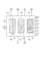
- FIG. 1 is a schematic diagram showing a planar layout configuration of a display device according to an embodiment of the present invention
- FIG. 1 is a schematic plan view showing a pixel configuration of a display device according to an embodiment of the invention
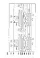
- FIG. 1 is a schematic cross-sectional view of a pixel of a display device according to an embodiment of the invention
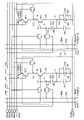
- FIG. 1 is a circuit diagram showing the circuit configuration of a pixel of a display device according to an embodiment of the invention
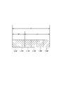
- FIG. FIG. 4 is a schematic diagram illustrating control of pixel gradation in one frame period using a first gradation control mode in the display device according to one embodiment of the present invention.
- FIG. 1 is a schematic diagram showing a planar layout configuration of a display device according to an embodiment of the present invention
- FIG. 1 is a schematic plan view showing a pixel configuration of a display device according to an embodiment of the invention
- FIG. 1 is a schematic cross-sectional view of a pixel of a display device according to an embodiment of
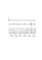
- FIG. 5 is a schematic diagram illustrating control of pixel gradation in one frame period using a second gradation control mode in the display device according to one embodiment of the present invention.
- FIG. 10 is a schematic diagram illustrating control of pixel gradation in one frame period using a third gradation control mode in the display device according to one embodiment of the present invention.
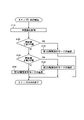
- FIG. 4 is a flow chart diagram showing selection processing of a gradation control mode executed by the gradation control circuit section of the display device according to one embodiment of the present invention.
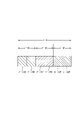
- 1 is a schematic cross-sectional view of a pixel of a display device according to an embodiment of the invention; FIG. FIG.
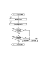
- FIG. 4 is a flow chart diagram showing calculation processing of an average illuminance value executed by the gradation control circuit section of the display device according to one embodiment of the present invention.
- FIG. 4 is a flow chart diagram showing selection processing of a gradation control mode executed by the gradation control circuit section of the display device according to one embodiment of the present invention.
- ⁇ includes A, B or C
- ⁇ includes any one of A, B and C
- ⁇ includes one selected from the group consisting of A, B and C
- ⁇ does not exclude the case where ⁇ includes a plurality of combinations of A to C, unless otherwise specified.
- these expressions do not exclude the case where ⁇ contains other elements.
- the terms “upper”, “upper”, “lower”, and “lower” are used, but in principle, the substrate on which the structure is formed is used as a reference, and the structure is formed from the substrate. Let the direction toward an object be “up” or “upper”. Conversely, the direction from the structure toward the substrate is defined as “down” or “lower”. Therefore, in the expression of the structure on the substrate, the surface of the structure facing the substrate is the lower surface of the structure, and the opposite surface is the upper surface of the structure.
- the expression “structure on the substrate” merely describes the vertical relationship between the substrate and the structure, and other members may be arranged between the substrate and the structure.
- the terms “upper” or “upper” or “lower” or “lower” mean the order of stacking in a structure in which a plurality of layers are stacked, even if they are not in an overlapping positional relationship in plan view. good.
- display device broadly includes devices for displaying images, and includes not only display panels and display modules, but also other optical members (e.g., polarizing members, backlights, touch panels, or biological devices). may also include devices with attached authentication sensors, etc.).
- FIG. 10 A display device 10 according to an embodiment of the present invention will be described with reference to FIGS. 1 to 8.
- FIG. 1 A display device 10 according to an embodiment of the present invention will be described with reference to FIGS. 1 to 8.
- FIG. 10 A display device 10 according to an embodiment of the present invention will be described with reference to FIGS. 1 to 8.
- FIG. 1 A display device 10 according to an embodiment of the present invention will be described with reference to FIGS. 1 to 8.
- FIG. 1 is a schematic plan view showing the configuration of a display device 10 according to one embodiment of the invention.
- the display device 10 includes a display section 100, an illuminance detection section 200, a gradation control circuit section 300, a video signal line drive circuit section 400, a scanning signal line drive circuit section 500, and a terminal section 600.
- the illuminance detection section 200 , the gradation control circuit section 300 , the video signal line drive circuit section 400 , the scanning signal line drive circuit section 500 and the terminal section 600 are provided around the display section 100 .
- the area around the display unit 100 may be called a non-display area, a frame area, or the like.
- the display unit 100 can display images.
- the display unit 100 includes multiple pixels 110 .
- the plurality of pixels 110 are arranged in a matrix, for example, but the arrangement of the plurality of pixels 110 is not limited to this.
- Each of the plurality of pixels 110 includes a first LED chip 120 , a second LED chip 130 and a transistor 140 . The details of the structures of the first LED chip 120, the second LED chip 130, and the transistor 140 will be described later.
- the first LED chip 120 and the second LED chip 130 have the same emission color.
- Each of first LED chip 120 and second LED chip 130 is one of a red LED chip, a green LED chip, and a blue LED chip. That is, each of the plurality of pixels 110 has one emission color of red emission, green emission, and blue emission. By controlling the emission color and gradation of each of the plurality of pixels 110, the display unit 100 can display a full-color image.
- the sizes of the first LED chip 120 and the second LED chip 130 are not particularly limited. Considering the size or resolution of the display device 10, the size of the first LED chip 120 and the second LED chip 130 may be determined. For example, if the display device 10 is a small-to-medium display device, a mini LED chip or a micro LED chip can be used.
- the first LED chip 120 and the second LED chip 130 may be LED chips of the same size or LED chips of different sizes. In addition, below, for convenience, the first LED chip 120 and the second LED chip 130 are described as LED chips having the same size.
- the illuminance detection unit 200 can detect the illuminance value of external light.
- the illuminance detection unit 200 is, for example, an illuminance sensor.
- the gradation control circuit section 300 can determine the illuminance value and select the gradation control mode. Also, a signal for controlling the pixel 110 can be generated according to the selected gradation control mode.
- the video signal line drive circuit section 400 and the scanning signal line drive circuit section 500 drive the transistors 140 included in the pixels 110 to control light emission or non-light emission of the first LED chip 120 and the second LED chip 130. can be done.
- the terminal section 600 includes a plurality of terminals 610 and can be electrically connected to an external device. That is, the display device 10 can be supplied with power or signals from an external device via the terminal section 600 .
- FIG. 2 is a schematic plan view showing the configuration of the pixel 110 of the display device 10 according to one embodiment of the invention.
- FIG. 2 shows a pixel unit including red pixel 110R, green pixel 110G, and blue pixel 110B.
- the red pixel 110R includes a first red LED chip 120R and a second red LED chip 130R.
- Green pixel 110G includes a first green LED chip 120G and a second green LED chip 130G.
- Blue pixel 110B includes a first blue LED chip 120B and a second blue LED chip 130B. Note that hereinafter, pixels, first LED chips, and second LED chips may be referred to as pixels 110, first LED chips 120, and second LED chips 130 when colors are not particularly distinguished. be.
- the scanning signal line driving circuit section 500 supplies the scanning signal SG(n), the light emission control signal BG(n), An initialization control signal IG(n) and a first reset signal RG(n) may be provided.
- the first reset signal RG(n) can supply the voltage Vrst to the pixel units located in the n-th row in the display section 100 .
- the reference voltage line PVSS can commonly supply the reference voltage VSS to the pixel units.
- the reset signal VL1 can commonly supply the voltage Vrst to the pixel units.
- the video signal line driving circuit section 400 commonly supplies the video signal SL(m) and the second reset signal VL2 to the pixel units located in the m-th column (m is an integer equal to or greater than 1) in the display section 100. can do.
- the second reset signal VL2 can supply the voltage Vini to the pixel unit located in the m-th column in the display section 100.
- the first drive power supply line PVDD1 can supply the first drive voltage VDDH1 to the pixel unit located in the m-th column in the display section 100.
- the second drive power supply line PVDD2 can supply the second drive voltage VDDH2 to the pixel unit located in the m-th column in the display section 100.
- the third drive power supply line PVDD3 can supply the third drive voltage VDDH3 to the pixel unit located in the m-th column in the display section 100.
- FIG. A fourth drive power supply line PVDD4 can supply a fourth drive voltage VDDH4 to the pixel unit located in the m-th column in the display section 100 .
- the fifth drive power supply line PVDD5 can supply the fifth drive voltage VDDH5 to the pixel unit located in the m-th column in the display section 100.
- the sixth drive power supply line PVDD6 can supply the sixth drive voltage VDDH6 to the pixel unit located in the m-th column in the display section 100.
- the scanning signal line driver circuit portion 500 supplies the pixel units with the first reset signal RG
- the video signal line driver circuit portion 400 supplies the pixel units with the second reset signal VL2. supply, but is not limited to.
- the video signal line driving circuit section 400 may supply the pixel units with the first reset signal RG
- the scanning signal line driving circuit section 500 may supply the pixel units with the second reset signal VL2. good.
- either one of the scanning signal line driving circuit section 500 and the video signal line driving circuit section 400 may supply the first reset signal RG and the second reset signal VL2 to the pixel unit.
- the first reset signal RG and the second reset signal VL2 may be electrically connected to the terminal 610.
- the voltage Vrst may be called a reset voltage.
- the voltage Vini may be referred to as an initialization voltage.
- the drive power supply line PVDD6 is provided in the video signal line drive circuit section 400 and includes a first drive voltage VDDH1, a second drive voltage VDDH2, a third drive voltage VDDH3, a fourth drive voltage VDDH4, a fifth drive voltage VDDH4, and a fifth drive voltage VDDH4.
- the voltage VDDH5 and the sixth drive voltage VDDH6 are supplied from the video signal line drive circuit section 400 to the pixel units, but are not limited to this.
- the first drive power supply line PVDD1, the second drive power supply line PVDD2, the third drive power supply line PVDD3, the fourth drive power supply line PVDD4, the fifth drive power supply line PVDD5, and the sixth drive power supply line PVDD6 are may be provided in the scanning signal line driving circuit portion 500, and include a first driving voltage VDDH1, a second driving voltage VDDH2, a third driving voltage VDDH3, a fourth driving voltage VDDH4, a fifth driving voltage VDDH5, and A part of the sixth driving voltage VDDH6 may be provided in the scanning signal line driving circuit section 500 and the rest may be provided in the video signal line driving circuit section 400 .
- the arrangement of the power supply lines may be appropriately changed according to the application or specifications.
- FIG. 3 is a schematic cross-sectional view of the pixel 110 of the display device 10 according to one embodiment of the invention. Specifically, FIG. 3 is a schematic cross-sectional view of the pixel 110 cut along line A1-A2 shown in FIG.
- the pixel 110 includes a substrate 1000, a light shielding layer 1010, an undercoat layer 1020, a semiconductor layer 1030, a first insulating layer 1040, a first conductive layer 1050, a second insulating layer 1060, a second conductive layer 1070, first planarization layer 1080, third conductive layer 1090, third insulating layer 1100, fourth conductive layer 1110, fifth conductive layer 1120, sixth conductive layer 1130, first LED chip 120 , second LED chip 130 , second planarization layer 1140 , seventh conductive layer 1150 and overcoat layer 1160 .
- the substrate 1000 can support each layer provided on the substrate 1000 .
- Substrate 1000 may be a substrate that can transmit light emitted from first LED chip 120 or second LED chip 130 .
- a light-transmitting rigid substrate such as a glass substrate, a quartz substrate, or a sapphire substrate can be used.
- a non-light-transmitting rigid substrate such as a silicon substrate can be used.
- a light-transmitting flexible substrate such as a polyimide resin substrate, an acrylic resin substrate, a siloxane resin substrate, or a fluororesin substrate can be used.
- impurities may be introduced into the above resin substrate.
- a substrate in which a silicon oxide film or a silicon nitride film is formed over a rigid substrate or flexible substrate described above can also be used as the substrate 1000 .
- the light shielding layer 1010 can reflect or absorb external light.
- a material of the light shielding layer 1010 for example, aluminum (Al), copper (Cu), titanium (Ti), molybdenum (Mo), tungsten (W), alloys or compounds thereof, or the like can be used.
- a black matrix can be used as a material of the light shielding layer 1010.
- the light shielding layer 1010 may have a laminated structure as well as a single layer structure. For example, the light shielding layer 1010 may have a laminated structure of red color filters, green color filters, and blue color filters.
- the undercoat layer 1020 can prevent impurities from diffusing into the semiconductor layer 1030 .
- a material for the undercoat layer 1020 for example, silicon oxide or silicon nitride can be used.
- the undercoat layer 1020 may be a single layer or a laminate. Note that a configuration in which the undercoat layer 1020 is not provided can also be employed.
- the semiconductor layer 1030 , the first insulating layer 1040 , the first conductive layer 1050 , the second insulating layer 1060 , and the second conductive layer 1070 include the configuration of the so-called transistor 140 . That is, the semiconductor layer 1030, the first insulating layer 1040, the first conductive layer 1050, the second insulating layer 1060, and the second conductive layer 1070 are respectively a semiconductor film, a gate insulating film, a gate electrode, and an interlayer insulating layer. It can function as a membrane and a source or drain electrode.
- the transistor 140 shown in FIG. 3 is a top-gate transistor.
- a first insulating layer 1040 (gate insulating film) is provided over the semiconductor layer 1030 (semiconductor film).
- a first conductive layer 1050 (gate electrode) is provided over the first insulating layer 1040 (gate insulating film).
- a second insulating layer 1060 (interlayer insulating film) is provided over the first conductive layer 1050 (gate electrode).
- a second conductive layer 1070 source electrode or drain electrode
- the second conductive layer 1070 (source electrode or drain electrode) is electrically connected to the semiconductor layer 1030 (semiconductor film) through the opening.
- the transistor 140 included in the pixel 110 is not limited to a top-gate transistor.
- Transistor 140 may be a bottom-gate transistor.
- a dual-gate transistor having two gate electrodes with insulating layers provided above and below the semiconductor layer 1030 interposed therebetween may be used.
- the first conductive layer 1050 is used as the first gate electrode
- the light blocking layer 1010 is used as the second gate electrode.
- a semiconductor material capable of forming a channel region can be used as the material of the semiconductor layer 1030 .
- the semiconductor material for example, silicon, an oxide semiconductor such as indium gallium zinc oxide (IGZO) or zinc oxide (ZnO), or a compound semiconductor such as gallium arsenide (GaAs) or gallium nitride (GaN) can be used.
- the semiconductor material is silicon, the semiconductor material can be amorphous silicon, polysilicon, or single crystal silicon.
- the semiconductor layer 1030 may include not only a channel region but also a source region or a drain region (high concentration impurity region). Furthermore, a low concentration impurity region may be included between the channel region and the source region or between the channel region and the drain region.
- first insulating layer 1040 and the second insulating layer 1060 for example, silicon oxide, silicon nitride, aluminum oxide, hafnium oxide, or aluminum nitride can be used. Also, the first insulating layer 1040 or the second insulating layer 1060 may be a single layer or a laminated layer.
- a metal material can be used as a material for each of the first conductive layer 1050 and the second conductive layer 1070 .
- metal materials include copper (Cu), aluminum (Al), titanium (Ti), chromium (Cr), cobalt (Co), nickel (Ni), molybdenum (Mo), hafnium (Hf), tantalum (Ta ), tungsten (W), or bismuth (Bi), or alloys or compounds thereof.
- the first conductive layer 1050 and the second conductive layer 1070 may be single layers or stacked layers.
- the first planarization layer 1080 can planarize unevenness of the transistor 140 .
- a first planarization layer 1080 is provided over the second conductive layer 1070 .
- the first planarization layer 1080 may optionally have openings to expose a portion of the second conductive layer 1070 .
- an acrylic resin, a silicone resin, a polyimide resin, or the like can be used as a material of the first planarization layer 1080.
- the third conductive layer 1090 can function as a common electrode.
- a transparent conductive material such as indium tin oxide (ITO) or indium zinc oxide (IZO) can be used.
- the third insulating layer 1100 can function as a capacitor dielectric.
- a material of the third insulating layer 1100 for example, silicon nitride or the like can be used.
- the fourth conductive layer 1110 can function as a pixel electrode.
- a transparent conductive material such as indium tin oxide (ITO) or indium zinc oxide (IZO) can be used.
- the fifth conductive layer 1120 can function as an anode.
- a transparent conductive material such as indium tin oxide (ITO) or indium zinc oxide (IZO), or a metal material such as silver (Ag) can be used.
- the fifth conductive layer 1120 can also have a laminated structure of these materials. For example, a structure such as ITO/Ag/ITO can be used as the laminated structure.
- the sixth conductive layer 1130 functions as a connection layer that connects the electrode provided on the first LED chip 120 or the second LED chip 130 and the fifth conductive layer 1120 provided on the substrate 1000 side. be able to.
- a material of the sixth conductive layer 1130 for example, silver paste or solder can be used.
- the second planarization layer 1140 can planarize unevenness of the first LED chip 120 or the second LED chip 130 .
- a material of the second planarization layer 1140 for example, an acrylic resin, a polyimide resin, an epoxy resin, a silicone resin, or the like can be used.
- the seventh conductive layer 1150 can function as a cathode.
- a transparent conductive material such as indium tin oxide (ITO) or indium zinc oxide (IZO) can be used.
- the overcoat layer 1160 can reduce external influences (moisture, impact, etc.).
- a material for the overcoat layer 1160 an inorganic material such as silicon nitride or an organic material such as acrylic resin or polyimide resin can be used.
- the overcoat layer 1160 can also have a laminated structure of these materials.
- FIG. 4 is a circuit diagram showing the circuit configuration of the pixel 110 of the display device 10 according to one embodiment of the invention.
- the pixel 110 has a first driver 121 and a second LED chip and second driver 131 that control the first LED chip 120 .
- the configuration of the second drive unit 131 is such that the LED chip is the second LED chip 130, the holding capacitive element is the holding capacitive element SC2, and the drive power line is the second drive power line PVDD2.
- the configuration is different from that of the first driving section 121 .
- the configuration of the second drive section 131 is the same as that of the first drive section 121 except for the LED chip, the holding capacitor element, and the drive power source.
- the first drive unit 121 includes a drive transistor DRT, a selection transistor SST (first switch), an initialization transistor IST (second switch), a reset transistor RST (third switch), and a light emission control transistor. It includes a BCT (fourth switch), a holding capacitive element (capacitive element) SC1, a first LED chip 120, a cathode capacitance Ccd, and an additional capacitance Cel. Each of these transistors includes a first electrode (gate electrode) and a pair of electrodes (source electrode, drain electrode) consisting of a second electrode and a third electrode. Each of holding capacitive element SC1, cathode capacity Ccd, and additional capacity Cel includes a pair of electrodes. Note that the additional capacitance Cel may be the parasitic capacitance of the first LED chip 120, and may include the capacitive element provided in parallel with the first LED chip 120 and the parasitic capacitance of the first LED chip 120. .
- the first drive voltage VDDH1 is supplied from the first drive power supply line PVDD1
- the reference voltage VSS is supplied from the reference voltage line PVSS, and reset.
- a voltage Vrst is supplied from the signal VL1.
- a second drive voltage VDDH2 is supplied from the second drive power supply line PVDD2. The voltage Vrst is lower than the first drive voltage VDDH1 and the second drive voltage VDDH2, and can be substantially the same as the reference voltage VSS.
- the first drive voltage VDDH1 may be higher than the second drive voltage VDDH2
- the third drive voltage VDDH3 may be higher than the fourth drive voltage VDDH4
- the fifth drive power supply line PVDD5 is the sixth drive voltage. It may be higher than the voltage VDDH6.
- the driving transistor DRT has a function of causing a current to flow through the first LED chip 120 using the input video signal to cause the first LED chip 120 to emit light.
- the select transistor SST has a function of supplying a video signal to the drive transistor DRT.
- the initialization transistor IST has a function of supplying a voltage Vini to the first electrode 141 (gate electrode 141) of the drive transistor DRT and resetting the drive transistor DRT.
- the light emission control transistor BCT controls connection or disconnection between the first drive power supply line PVDD1 or the second drive power supply line PVDD2 and the drive transistor DRT.
- the light emission control transistor BCT controls electrical connection or disconnection between the drive transistor DRT and the first LED chip 120, and between the drive transistor DRT and the additional capacitor Cel.
- the light emission control transistor BCT of the first driving section 121 has a function of controlling light emission or non-light emission of the first LED chip 120 .
- a second drive voltage VDDH2 is supplied from the second drive power supply line PVDD2. That is, the light emission control transistor BCT of the second driving section 131 has a function of controlling light emission or non-light emission of the second LED chip 130 .
- the reset transistor RST supplies the voltage Vrst to the third electrode 142 (drain electrode 142) of the drive transistor DRT, supplies the voltage Vrst to the first electrode 122 of the first LED chip 120, and supplies the voltage Vrst to the first electrode 142 of the drive transistor DRT. 2 electrode 143 (source electrode 143 ) and the function of resetting the first LED chip 120 .
- a first electrode 122 of the first LED chip 120 is, for example, an anode.
- the reset transistor RST of the second driving section 131 supplies the voltage Vrst to the first electrode 132 of the second LED chip 130 and has the same function as the reset transistor RST of the first driving section 121 .
- the holding capacitive element SC1 has a function of securing a voltage corresponding to the threshold of the driving transistor DRT. Further, the holding capacitive element SC1 has a function of maintaining the voltage input to the first electrode 141 (gate electrode 141) of the driving transistor DRT in order for the first LED chip 120 to emit light. That is, the holding capacitive element SC1 has a function of holding the input video signal. Further, the holding capacitive element SC2 has a configuration similar to that of the holding capacitive element SC1 and has a similar function.
- the display device 10 has a holding capacitive element such as a holding capacitive element SC2 or a holding capacitive element SC1 for holding an input video signal. It does not have to be a holding capacitive element.
- a holding capacitive element such as a holding capacitive element SC2 or a holding capacitive element SC1 for holding an input video signal. It does not have to be a holding capacitive element.
- an element capable of holding a signal or voltage may be an element capable of holding binary data such as an SRAM.
- the first LED chip 120 has diode characteristics.
- the additional capacitance Cel is the capacitance included in the first LED chip 120 .
- the cathode capacitance Ccd is a capacitance formed between the first electrode 122 of the first LED chip 120 and the reference voltage line PVSS.
- the second LED chip 130 has a diode characteristic like the first LED chip 120 .
- the additional capacitance Cel of the second driving section 131 is also the capacitance included in the second LED chip 130 .
- the cathode capacitance Ccd of the second drive section 131 is also the capacitance formed between the first electrode 132 of the second LED chip 130 and the reference voltage line PVSS.
- the input video signal may be held by the additional capacitor Cel and the holding capacitor element SC1 or SC2.
- a gate electrode of the initialization transistor IST is electrically connected to the initialization control line 416 .
- An initialization control signal IG(n) is supplied to the initialization control line 416 .
- the initialization transistor IST is controlled between a conducting state and a non-conducting state by a signal supplied as the initialization control signal IG(n).
- the signal supplied to the initialization control signal IG(n) is at low level (L level)
- the initialization transistor IST is in a non-conducting state.
- the signal supplied to the initialization control signal IG(n) is at a high level (High Level, H level)
- the initialization transistor IST becomes conductive.
- a source electrode of the initialization transistor IST is electrically connected to the second reset voltage line 414 .
- a second reset signal VL ⁇ b>2 is supplied to the second reset voltage line 414 .
- the drain electrode of the initialization transistor IST is electrically connected to the gate electrode 141 of the drive transistor DRT, the drain electrode of the select transistor SST, and the first electrode 144 of the storage capacitor SC1.
- the second electrode 145 of the storage capacitor SC1 is connected to the source electrode 143 of the drive transistor DRT, the drain electrode of the reset transistor RST, the first electrode 122 of the first LED chip 120, and the first electrode of the additional capacitor Cel. electrically connected.
- the second electrode 145 of the storage capacitor SC2 is the source electrode 143 of the drive transistor DRT of the second drive section 131, the drain electrode of the reset transistor RST of the second drive section 131, and the first electrode of the second LED chip 130. and the first electrode of the additional capacitor Cel.
- a gate electrode of the selection transistor SST is electrically connected to the scanning signal line 408 .
- a scanning signal SG(n) is supplied to the scanning signal line 408 .
- the selection transistor SST is controlled to be in a conducting state or a non-conducting state by a signal supplied to the scanning signal SG(n).
- the select transistor SST becomes non-conductive.
- the select transistor SST is in a conducting state.
- a source electrode of the select transistor SST is electrically connected to the video signal line 409 .
- a video signal SL(m) is supplied to the video signal line 409 .
- a gate electrode of the light emission control transistor BCT is electrically connected to the light emission control line 418 .
- a light emission control signal BG(n) is supplied to the light emission control line 418 .
- the light emission control transistor BCT is controlled to be conductive or non-conductive by a signal supplied as the light emission control signal BG(n).
- the signal supplied to the light emission control signal BG(n) is at L level, the light emission control transistor BCT becomes non-conductive.
- the signal supplied to the light emission control signal BG(n) is at H level, the light emission control transistor BCT becomes conductive.
- a drain electrode of the light emission control transistor BCT is electrically connected to the first drive power supply line PVDD1 or the second drive power supply line PVDD2.
- the first drive power supply line PVDD1 is the first drive power supply line 428 .
- the second drive power line PVDD2 is the second drive power line 429 .
- a source electrode of the light emission control transistor BCT is electrically connected to the drain electrode 142 of the drive transistor DRT.
- a gate electrode of the reset transistor RST is electrically connected to the first reset signal line 412 .
- a first reset signal RG is supplied to the first reset signal line 412 .
- the conductive state and non-conductive state of the reset transistor RST are controlled by a signal supplied to the first reset signal line 412 .
- the reset transistor RST becomes non-conductive.
- the reset transistor RST becomes conductive.
- a source electrode of the reset transistor RST is electrically connected to the first reset voltage line 410 .
- a first reset signal VL1 is supplied to the first reset voltage line 410 .
- the second electrode 123 of the first LED chip 120, the cathode capacitance Ccd, and the second electrodes of the additional capacitance Cel are electrically connected to the reference voltage line PVSS.
- the reference voltage line PVSS is electrically connected to the cathode, for example.
- the second electrode 133 of the second LED chip 130 like the second electrode 123 of the first LED chip 120, is connected to the reference voltage line PVSS by the second electrodes of the cathode capacitance Ccd and the additional capacitance Cel. is electrically connected to
- the drain electrode of the initialization transistor IST, the drain electrode of the select transistor SST, the gate electrode 141 of the drive transistor DRT, and the first electrode 144 of the storage capacitor SC1 are electrically connected to the first node A.
- the source electrode 143 of the drive transistor DRT, the second electrode of the storage capacitor element Cs, the first electrode 122 of the first LED chip 120, and the first electrode of the additional capacitor Cel are electrically connected to the third node C.
- connected to A drain electrode of the reset transistor RST, a drain electrode 142 of the drive transistor DRT, and a source electrode of the light emission control transistor BCT are electrically connected to the second node B.
- the first reset voltage line 410 supplies a common voltage Vrst to the pixels 110, it may be referred to as a second common electrode in this specification and the like. Because the second reset voltage line 414 supplies a common voltage Vini to the pixels 110, it may be referred to herein as a third common electrode. Note that the voltage Vrst and the voltage Vini are substantially the same voltage. Since the voltage Vrst and the voltage Vini are substantially the same, the voltage of the gate electrode 141 of the driving transistor DRT and the voltage of the source electrode 143 of the driving transistor DRT can be substantially the same when the driving transistor DRT is reset. Both the reset of the drive transistor DRT and the threshold correction of the drive transistor DRT can be performed with high accuracy.
- a conductive state indicates a state in which the source electrode and the drain electrode of a transistor are electrically connected and the transistor is on.
- a non-conducting state refers to a state in which the source electrode and the drain electrode of a transistor are out of conduction and the transistor is off. Note that in each transistor, the source electrode and the drain electrode may be switched depending on the voltage of each electrode. A person skilled in the art can easily understand that a small amount of current such as leakage current flows even when the transistor is off.
- the gradation control circuit section 300 selects a gradation control mode, and the gradation of the pixels 110 is controlled based on the gradation control mode.
- the grayscale control mode includes multiple control methods for controlling the grayscale of the pixels 110 . Control methods include, for example, an area control method, a pulse width modulation (PWM) control method, or a current control method.
- PWM pulse width modulation
- the gradation of pixels is controlled by the light emitting area of the LED chip. That is, in the display device 10, the gradation of the pixel 110 is controlled by whether the first LED chip 120 or the second LED chip 130 emits light or not. For the sake of convenience, the following description assumes that the number of gradations is 2 bits.
- Control of light emission of the first LED chip 120 is assigned to one of the two bits (hereinafter referred to as "0th bit”). That is, the 0th bit can control the gradation of the pixel 110 depending on whether the first LED chip 120 emits light or not.
- the other bit of the two bits (hereinafter referred to as “first bit”) is assigned to control light emission of both the first LED chip 120 and the second LED chip 130 . That is, the first bit can control the gradation of the pixel 110 by emitting or not emitting light from both the first LED chip 120 and the second LED chip 130 . For the 0th bit, only the first LED chip 120 emits light, whereas for the first bit, both the first LED chip 120 and the second LED chip 130 emit light.
- the light emitting area controlled by the first bit is the 0th bit. larger than the emission area controlled by Therefore, in the area control method, by controlling whether the first LED chip 120 or the second LED chip 130 emits light or not, four gradations as shown in Table 1 can be expressed.
- the voltage applied to the video signal SL(m) is kept constant, and light emission or non-light emission of the first LED chip 120 or the second LED chip 130 can be controlled by the light emission control transistor BCT.
- the number of gradations can be increased by increasing the number of LED chips.
- the gradation of pixels is controlled by the light emission time (pulse width) of the LED chip. That is, in the display device 10 , the gradation of the pixel 110 is controlled by the light emission time of the first LED chip and the second LED chip 130 .
- the number of gradations is 2 bits.
- a first pulse width is assigned to one of the two bits (hereinafter referred to as "0th bit”). That is, the 0th bit can control the gradation of the pixel 110 by turning on or off the first pulse width to cause the first LED chip 120 and the second LED chip 130 to emit light or not.
- a second pulse width is assigned to the other of the two bits (hereinafter referred to as "first bit”). That is, the first bit can control the gradation of the pixel 110 by turning on or off the second pulse width to cause the first LED chip 120 and the second LED chip 130 to emit light or not.
- the second pulse width is larger than the first pulse width.
- the light emission time of the first LED chip 120 and the second LED chip 130 in the 1st bit is longer than the light emission time of the first LED chip 120 and the second LED chip 130 in the 0th bit. Therefore, in the PWM control method, by controlling light emission or non-light emission of the first LED chip 120 and the second LED chip 130 by the first pulse width or the second pulse width, four levels as shown in Table 2 are obtained. tone can be expressed.
- the voltage applied to the video signal SL(m) is kept constant, and the pulse width of the signal supplied to the light emission control signal BG(n) connected to the gate electrode of the light emission control transistor BCT controls the first The light emission time of the LED chip 120 and the second LED chip 130 can be controlled.
- the number of gradations can be increased by increasing the number of pulse widths.
- the gradation of pixels is controlled by the current value supplied to the LED chip. That is, in the display device 10 , the gradation of the pixel 110 is controlled by the current value supplied to the first LED chip 120 and the second LED chip 130 .
- the number of gradations is 2 bits.
- a first current value is assigned to one of the two bits (hereinafter referred to as "0th bit”). That is, with the 0th bit, the gradation of the pixel 110 can be controlled by turning on or off the first current value to cause the first LED chip 120 and the second LED chip 130 to emit light or not.
- a second current value is assigned to the other of the two bits (hereinafter referred to as "first bit”). That is, the first bit can control the gradation of the pixel 110 by turning on or off the second current value to cause the first LED chip 120 and the second LED chip 130 to emit light or not.
- the second current value is greater than the first current value.
- the light emission brightness of the first LED chip 120 and the second LED chip 130 in the 1st bit is higher than the light emission brightness of the first LED chip 120 and the second LED chip 130 in the 0th bit. Therefore, in the current control method, by controlling light emission or non-light emission of the first LED chip 120 and the second LED chip 130 by the first current value or the second current value, four levels as shown in Table 3 are obtained. tone can be expressed.
- the current value supplied to the first LED chip 120 and the second LED chip 130 can be controlled by changing the voltage applied to the video signal SL(m).
- the number of gradations can be increased by increasing the number of current values.
- the gradation control mode may be selected according to the illuminance of the outside light, for example.
- the number of gradations is 6 bits.
- FIG. 5 is a schematic diagram illustrating grayscale control of the pixels 110 in one frame period using the first grayscale control mode in the display device 10 according to one embodiment of the present invention.
- one frame period (1F) is divided into a first subframe period (1SF) and a second subframe period (2SF).
- grayscale control of the pixels 110 is performed by the area control method.
- grayscale control of the pixels 110 is performed by the PWM control method.
- Each of the first subframe period (1SF) and the second subframe period (2SF) may be divided into a plurality of periods according to the number of gradations in the area control method and the PWM control method.
- 2 bits of the 6-bit grayscale number are assigned to the area control method, and 4 bits of the 6-bit grayscale number are assigned to the PWM control method.
- the first LED chip 120 or the second LED chip 130 emits or does not emit light.
- the gradation of the pixel 110 is controlled by light emission.
- the third period (2-1SF), the fourth period (2-2SF), the fifth period (2-3SF), and the sixth period (2-3SF) of the second subframe period (2SF) 4SF) the gradation of the pixel 110 is controlled by the first pulse width, the second pulse width, the third pulse width, and the fourth pulse width, respectively (here, the first pulse width> 2nd pulse width>3rd pulse width>4th pulse width). Therefore, Table 4 summarizes control of the gradation of the pixel 110 in each period (1-1SF to 2-4SF) within one frame period (1F) in the first gradation control mode.
- the number of gradations controlled by the PWM control method is large.
- the PWM driving method has the feature that the shift of the emission wavelength of the LED chip is small. Therefore, the control of the pixels 110 in the first gradation control mode is effective when the illuminance of the outside light is low and the shift of the emission wavelength is emphasized. Therefore, for example, when the outside light illuminance is 500 [lux] or less, the first gradation control mode is selected by the gradation control circuit section 300 .
- each period (1-1SF to 2-4SF) within one frame period (1F) may be the same or different.
- FIG. 6 is a schematic diagram illustrating grayscale control of the pixels 110 in one frame period using the second grayscale control mode in the display device 10 according to one embodiment of the present invention.
- one frame period (1'F) consists of a first subframe period (1'SF), a second subframe period (2'SF), and a third subframe period. (3'SF).
- first subframe period (1'SF) grayscale control of the pixels 110 is performed by the area control method.
- second sub-frame period (2'SF) grayscale control of the pixels 110 is performed by the PWM control method.
- third sub-frame period (3'SF) grayscale control of the pixel 110 is performed by the current control method.
- the first sub-frame period (1'SF), the second sub-frame period (2'SF), and the third sub-frame period (3'SF) are respectively the area control method, the PWM control method, and the current It may be divided into a plurality of periods according to the number of gradations in the control method.
- the second gradation control mode 2 bits of the 6-bit gradation number are assigned to the area control method, 3 bits of the 6-bit gradation number are assigned to the PWM control method, and 6-bit gradation number are assigned to the PWM control method.
- One bit of the grayscale number is assigned to the current control method.
- the first LED chip 120 or the second LED chip 130 The gradation of the pixel 110 is controlled by emitting or not emitting light. Also, in the third period (2'-1SF), the fourth period (2'-2SF), and the fifth period (2'-3SF) of the second subframe period (2'SF), , the fifth pulse width, the sixth pulse width, and the seventh pulse width control the gradation of the pixel 110 (here, the fifth pulse width>sixth pulse width>seventh pulse width
- the pulse width in the second gradation control mode may be the same as the pulse width in the first gradation control mode, for example, the sixth pulse width in the second gradation control mode.
- the seventh pulse width may be the first pulse width and the second pulse width of the first gradation control mode, respectively.).
- the gradation of the pixel 110 is controlled by the first current value. Therefore, the control of the gradation of the pixel 110 in each period (1'-1SF to 3'-1SF) within one frame period (1'F) in the second gradation control mode is summarized as shown in Table 5. is.
- the gradation of the pixel 110 can be controlled not only by the digital gradation control method of the area control method and the PWM control method, but also by the analog gradation control method of the current control method. Therefore, the control of the pixels 110 in the second gradation control mode is effective at ambient light illuminances where high emission luminance is required while shifts in emission wavelength are emphasized. Therefore, for example, when the ambient light illuminance exceeds 500 [lux] and is equal to or less than 5000 "lux", the gradation control circuit section 300 selects the second gradation control mode.
- each period (1'-1SF to 3'-1SF) within one frame period (1'F) may be the same or different.
- FIG. 7 is a schematic diagram illustrating grayscale control of the pixels 110 in one frame period using the third grayscale control mode in the display device 10 according to one embodiment of the present invention.
- one frame period (1''F) consists of a first subframe period (1''SF), a second subframe period (2''SF), and a third subframe period (2''SF). It is divided into subframe periods (3′′SF).
- first sub-frame period (1′′SF) grayscale control of the pixels 110 is performed by the area control method.
- second sub-frame period (2′′SF) grayscale control of the pixels 110 is performed by the PWM control method.
- third sub-frame period (3′′SF) grayscale control of the pixel 110 is performed by the current control method.
- the first sub-frame period (1''SF), the second sub-frame period (2''SF), and the third sub-frame period (3''SF) are respectively controlled by the area control method and the PWM control method. , and the number of gradations in the current control method, it may be divided into a plurality of periods.
- the third gradation control mode 2 bits of the 6-bit gradation number are assigned to the area control method, 2 bits of the 6-bit gradation number are assigned to the PWM control method, and 6-bit gradation number are assigned to the PWM control method. Two bits of the grayscale number are assigned to the current control method.
- the first LED chip 120 or the second The gradation of the pixel 110 is controlled by whether the LED chip 130 emits light or not.
- the eighth pulse width and the ninth are equal to the first grayscale. It may be the same as the pulse width of the control mode or the second grayscale control mode, for example, the 9th pulse width of the third grayscale control mode may be the same as the fifth pulse width of the second grayscale control mode.
- the second current value and the third The gradation of the pixel 110 is controlled by the current value of .
- Table 6 summarizes control of the gradation of the pixel 110 in each period (1''-1SF to 3''-2SF) within one frame period (1''F) in the third gradation control mode. as shown in
- the control of the pixels 110 in the third gradation control mode is effective when the illuminance of the external light is high and the magnitude of the emission luminance is emphasized. Therefore, for example, when the external light illuminance exceeds 5000 [lux], the third gradation control mode is selected by the gradation control circuit section 300 .
- the length of each period (1''-1SF to 3''-2SF) within one frame period (1''F) may be the same or different.
- the grayscale control mode selection process executed by the grayscale control circuit unit 300 of the display device 10 according to the present embodiment will be described.
- the gradation control circuit section 300 selects any one of the above-described first to third gradation control modes.
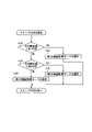
- FIG. 8 is a flowchart showing the grayscale control mode selection process (step S100) executed by the grayscale control circuit section 300 of the display device 10 according to one embodiment of the present invention.
- the gradation control circuit section 300 acquires the illuminance value of the outside light generated by the illuminance detection section 200 (step S110). Next, the gradation control circuit unit 300 determines whether or not the acquired illuminance value is equal to or less than the first value (step S120). If the illuminance value is equal to or less than the first value (step S120: YES), the gradation control circuit section 300 selects the first gradation control mode (step S130). When the first gradation control mode is selected, step S100 ends.
- step S120 When the illuminance value exceeds the first value (step S120: NO), the gradation control circuit section 300 determines whether the illuminance value is equal to or less than the second value (step S140). If the illuminance value is less than or equal to the second value (step S140: YES), the gradation control circuit section 300 selects the second gradation control mode (step S150). When the second gradation control mode is selected, step S100 ends.
- step S140 When the illuminance value exceeds the second value (step S140: NO), the gradation control circuit section 300 selects the third gradation control mode (step S160). When the third gradation control mode is selected, step S100 ends.
- the gradation control circuit section 300 generates a signal for controlling the gradation of the pixel 110 according to the selected first to third gradation control modes.
- the first value is, for example, 500 [lux].
- the second value is, for example, 5000 [lux].
- the first value and the second value are not limited to this.
- the grayscale control mode is selected by the grayscale control circuit section 300 .
- the image quality required for display on the display unit 100 varies depending on the illuminance value of the outside light.
- the gradation of the pixel 110 can be controlled according to the illuminance value. Therefore, the display unit 100 of the display device 10 can display with excellent visibility.
- the first LED chip 120 and the second LED chip 130 of the display device 10 are not limited to the same LED chip. Therefore, in the present embodiment, a first LED chip 120A and a second LED chip 130A having the same size but different element structures will be described with reference to FIG. In addition, below, when the structure of this embodiment is the same as the structure of 1st Embodiment mentioned above, description of the structure of this embodiment may be abbreviate
- FIG. 9 is a schematic cross-sectional view of a pixel 110A of the display device 10 according to one embodiment of the invention.
- the pixel 110A includes a first LED chip 120A and a second LED chip 130A.
- a first resistive film 125A and a second resistive film 135A are provided on the first LED chip 120A and the second LED chip 130A, respectively.
- the area where the first resistive film 125A contacts the first LED chip 120A is larger than the area where the second resistive film 135A contacts the second LED chip 130A. Therefore, the amount of charge injected into the first LED chip 120A is smaller than the amount of charge injected into the second LED chip 130A. That is, when the same voltage is applied to the first LED chip 120A and the second LED chip 130, the current supplied to the first LED chip 120A is equal to the current supplied to the second LED chip 130A. less than value.
- the gradation of pixel 110 may be controlled by light emission or non-light emission of each of first LED chip 120A and second LED chip 130A.
- the number of gradations is 2 bits.
- One of the two bits (hereinafter referred to as "the 0th bit”) is assigned to control the light emission of the first LED chip 120A. That is, the 0th bit can control the gradation of the pixel 110 depending on whether the first LED chip 120A emits light or not.
- the other bit of the two bits (hereinafter referred to as "first bit") is assigned to control light emission of the second LED chip 130A. That is, the first bit can control the gradation of the pixel 110 depending on whether the second LED chip 130A emits light or not.
- the light emitting area of the second LED chip 130A controlled by the first bit is larger than the light emitting area of the first LED chip 120A controlled by the 0th bit. Therefore, in the area control method of the present embodiment, it is possible to express four gradations as shown in Table 7 by controlling light emission or non-light emission of each of the first LED chip 120A and the second LED chip 130A. can.
- the number of gradations can be increased by increasing the number of LED chips.
- the first LED chip 120A and the second LED chip 130A of this embodiment have the same size, the first LED chip 120A and the second LED chip 130A can be transferred by the same method. can. Therefore, the display device 10 can be manufactured without changing the manufacturing method. Further, in the area control method, since each of the first LED chip 120A and the second LED chip 130A is assigned to a bit of the number of gradations, the frequency of light emission of the first LED chip 120A and the second LED chip 130A is not biased to any one. Therefore, since the first LED chip 120A and the second LED chip 130A deteriorate in substantially the same manner, variations in display on the display unit 100 can be reduced.
- the grayscale control circuit unit 300 of the display device 10 is not limited to the grayscale control mode selection process described in the first embodiment. Therefore, in the present embodiment, another grayscale control mode selection process executed by the grayscale control circuit unit 300 of the display device 10 will be described with reference to FIGS. 10 and 11. FIG. In addition, below, when the structure of this embodiment is the same as the structure of 1st Embodiment mentioned above, description of the structure of this embodiment may be abbreviate
- step S200 the average illuminance value calculation process
- step S300 the gradation control mode selection process
- the gradation control circuit section 300 acquires the illuminance value of the external light generated by the illuminance detection section 200 (step S210).
- the gradation control circuit unit 300 calculates an average illuminance value L ave_n of the illuminance values of the first to n-th frames (n is an integer equal to or greater than 2) (step S220).
- the gradation control circuit section 300 determines whether or not the average illuminance value Lave_n is monotonically increasing. For example, when the average illuminance value L ave_n in the nth frame is greater than the average illuminance value L ave_n ⁇ 1 in the n ⁇ 1th frame, it can be determined that the illumination is monotonously increasing.
- the average illuminance value L ave_n in the n-th frame is greater than the average illuminance value L ave_n-1 in the n-1-th frame, and
- the average illuminance value L ave_n ⁇ 1 is greater than the average illuminance value L ave_n ⁇ 2 in the n ⁇ 2th frame, it may be determined that the illuminance value monotonously increases.
- step S300 If the average illuminance value Lave_n is monotonically increasing (step S230: YES), a gradation control mode selection process is executed (step S300).
- the gradation control circuit unit 300 determines whether the average illuminance value Lave_n is monotonously decreasing. For example, when the average illuminance value L ave_n in the nth frame is smaller than the average illuminance value L ave_n ⁇ 1 in the n ⁇ 1th frame, it can be determined that the illumination is monotonously decreasing.
- the average illuminance value L ave_n in the n-th frame is smaller than the average illuminance value L ave_n-1 in the n-1-th frame, and
- the average illuminance value L ave_n ⁇ 1 is smaller than the average illuminance value L ave_n ⁇ 2 in the n ⁇ 2th frame, it may be determined that the illuminance value monotonously decreases.
- step S300 If the average illuminance value L ave_n is monotonously decreasing (step S240: YES), a gradation control mode selection process is executed (step S300).
- step S200 ends. In this case, the gradation control mode selection process is not executed. That is, control of the gradation of the pixel 110 is executed using the current gradation control mode.
- step S300 the gradation control mode selection process
- the gradation control circuit unit 300 determines whether or not the calculated average illuminance value Lave_n is equal to or less than the first value (step S310). If the average illuminance value Lave_n is equal to or less than the first value (step S310: YES), the gradation control circuit section 300 selects the first gradation control mode (step S320). If the first gradation control mode is selected, step S300 ends.
- step S310 When the average illuminance value Lave_n exceeds the first value (step S310: NO), the gradation control circuit unit 300 determines whether the average illuminance value Lave_n is equal to or less than the second value (step S330). ). If the average illuminance value Lave_n is equal to or less than the second value (step S330: YES), the gradation control circuit section 300 selects the second gradation control mode (step S340). If the second gradation control mode is selected, step S300 ends.
- step S330 When the average illuminance value Lave_n exceeds the second value (step S330: NO), the gradation control circuit section 300 selects the third gradation control mode (step S350). If the third gradation control mode is selected, step S300 ends.
- the gradation control circuit section 300 generates a signal for controlling the gradation of the pixel 110 according to the selected first to third gradation control modes.
- the first value is, for example, 500 [lux].
- the second value is, for example, 5000 [lux].
- the first value and the second value are not limited to this.
- the illuminance values acquired in a plurality of frames are averaged, and the average illuminance value is determined to select the gradation control mode.
- the gradation control mode is not switched with respect to changes in light). Therefore, it is possible to smoothly switch the gradation control mode.
- Display Device 100 Display Unit 110, 110A: Pixels 110B: Blue Pixels 110G: Green Pixels 110R: Red Pixels 120, 120A: First LED Chips 120B: First Blue LED Chips 120G: first green LED chip, 120R: first red LED chip, 121: first driving section, 122: first electrode, 123: second electrode, 125A: first resistive film, 130, 130A: second LED chip, 130B: second blue LED chip, 130G: second green LED chip, 130R: second red LED chip, 131: second driver, 132: first electrode, 133: Second electrode 135A: Second resistive film 140: Transistor 141: First electrode 142: Third electrode 143: Second electrode 144: First electrode 145: Second electrode 2 electrodes, 200: illuminance detection unit, 300: gradation control circuit unit, 400: video signal line drive circuit unit, 408: scanning signal line, 409: video signal line, 410: first reset voltage line, 412: First reset signal line 414: Second reset voltage line 416: Initialization control
Landscapes
- Engineering & Computer Science (AREA)
- Physics & Mathematics (AREA)
- General Physics & Mathematics (AREA)
- Theoretical Computer Science (AREA)
- Computer Hardware Design (AREA)
- Control Of Indicators Other Than Cathode Ray Tubes (AREA)
- Devices For Indicating Variable Information By Combining Individual Elements (AREA)
- Control Of El Displays (AREA)
- Led Device Packages (AREA)
- Led Devices (AREA)
Priority Applications (2)
| Application Number | Priority Date | Filing Date | Title |
|---|---|---|---|
| JP2022579364A JP7518928B2 (ja) | 2021-02-04 | 2021-12-07 | 表示装置 |
| US18/353,888 US12380836B2 (en) | 2021-02-04 | 2023-07-18 | Display device |
Applications Claiming Priority (2)
| Application Number | Priority Date | Filing Date | Title |
|---|---|---|---|
| JP2021016809 | 2021-02-04 | ||
| JP2021-016809 | 2021-02-04 |
Related Child Applications (1)
| Application Number | Title | Priority Date | Filing Date |
|---|---|---|---|
| US18/353,888 Continuation US12380836B2 (en) | 2021-02-04 | 2023-07-18 | Display device |
Publications (1)
| Publication Number | Publication Date |
|---|---|
| WO2022168431A1 true WO2022168431A1 (ja) | 2022-08-11 |
Family
ID=82741122
Family Applications (1)
| Application Number | Title | Priority Date | Filing Date |
|---|---|---|---|
| PCT/JP2021/045002 Ceased WO2022168431A1 (ja) | 2021-02-04 | 2021-12-07 | 表示装置 |
Country Status (3)
| Country | Link |
|---|---|
| US (1) | US12380836B2 (cg-RX-API-DMAC7.html) |
| JP (1) | JP7518928B2 (cg-RX-API-DMAC7.html) |
| WO (1) | WO2022168431A1 (cg-RX-API-DMAC7.html) |
Families Citing this family (2)
| Publication number | Priority date | Publication date | Assignee | Title |
|---|---|---|---|---|
| JPWO2022238797A1 (cg-RX-API-DMAC7.html) * | 2021-05-13 | 2022-11-17 | ||
| US12183280B2 (en) * | 2021-07-01 | 2024-12-31 | Universal Display Corporation | Means to reduce OLED transient response |
Citations (4)
| Publication number | Priority date | Publication date | Assignee | Title |
|---|---|---|---|---|
| EP2624243A1 (en) * | 2012-02-03 | 2013-08-07 | Ignis Innovation Inc. | Driving system for active-matrix displays |
| EP2889865A1 (en) * | 2013-12-31 | 2015-07-01 | LG Display Co., Ltd. | Hybrid driving method of an organic light emitting display apparatus |
| CN106652963A (zh) * | 2017-03-09 | 2017-05-10 | 南京迈智芯微光电科技有限公司 | 一种数模融合驱动的硅基显示器 |
| CN111354299A (zh) * | 2018-12-29 | 2020-06-30 | Tcl科技集团股份有限公司 | 一种led发光芯片的设计方法、装置及灰阶显示电路 |
Family Cites Families (6)
| Publication number | Priority date | Publication date | Assignee | Title |
|---|---|---|---|---|
| TWI539423B (zh) * | 2006-05-31 | 2016-06-21 | 半導體能源研究所股份有限公司 | 顯示裝置、顯示裝置的驅動方法、以及電子設備 |
| JP5422068B2 (ja) * | 2013-02-15 | 2014-02-19 | 三菱電機株式会社 | Led点灯装置および車両用前照灯 |
| JP2015011784A (ja) * | 2013-06-26 | 2015-01-19 | シャープ株式会社 | 照明装置 |
| JP2015094814A (ja) * | 2013-11-11 | 2015-05-18 | パイオニア株式会社 | 発光装置 |
| JP2019082549A (ja) * | 2017-10-30 | 2019-05-30 | シャープ株式会社 | フィールドシーケンシャル方式の画像表示装置および画像表示方法 |
| KR102538484B1 (ko) | 2018-10-04 | 2023-06-01 | 삼성전자주식회사 | 디스플레이 패널 및 디스플레이 패널의 구동 방법 |
-
2021
- 2021-12-07 JP JP2022579364A patent/JP7518928B2/ja active Active
- 2021-12-07 WO PCT/JP2021/045002 patent/WO2022168431A1/ja not_active Ceased
-
2023
- 2023-07-18 US US18/353,888 patent/US12380836B2/en active Active
Patent Citations (4)
| Publication number | Priority date | Publication date | Assignee | Title |
|---|---|---|---|---|
| EP2624243A1 (en) * | 2012-02-03 | 2013-08-07 | Ignis Innovation Inc. | Driving system for active-matrix displays |
| EP2889865A1 (en) * | 2013-12-31 | 2015-07-01 | LG Display Co., Ltd. | Hybrid driving method of an organic light emitting display apparatus |
| CN106652963A (zh) * | 2017-03-09 | 2017-05-10 | 南京迈智芯微光电科技有限公司 | 一种数模融合驱动的硅基显示器 |
| CN111354299A (zh) * | 2018-12-29 | 2020-06-30 | Tcl科技集团股份有限公司 | 一种led发光芯片的设计方法、装置及灰阶显示电路 |
Also Published As
| Publication number | Publication date |
|---|---|
| JP7518928B2 (ja) | 2024-07-18 |
| US20230360594A1 (en) | 2023-11-09 |
| JPWO2022168431A1 (cg-RX-API-DMAC7.html) | 2022-08-11 |
| US12380836B2 (en) | 2025-08-05 |
Similar Documents
| Publication | Publication Date | Title |
|---|---|---|
| US11538408B2 (en) | Organic light-emitting diode display | |
| CN107664862B (zh) | 显示装置及其制造方法 | |
| US10211264B2 (en) | Organic light emitting display device having a color filter on thin film transistor structure and method of manufacturing the same | |
| CN111326673B (zh) | 显示装置 | |
| US7855758B2 (en) | Liquid crystal display device | |
| US11362078B2 (en) | Display device | |
| CN119894286A (zh) | 显示设备 | |
| KR102914752B1 (ko) | 투명 마이크로 디스플레이 장치 | |
| US7994522B2 (en) | Organic light emitting element and organic light emitting device | |
| US20080068307A1 (en) | Gate and data drivers for display | |
| CN108269944B (zh) | 显示装置 | |
| US20060238461A1 (en) | Display device and driving method thereof | |
| US8013325B2 (en) | Thin film transistor, organic light emitting device including thin film transistor, and manufacturing method thereof | |
| US11811002B2 (en) | Display with dual red emitters | |
| US20220085137A1 (en) | Display device | |
| US20070126683A1 (en) | Display device and driving method therefor | |
| US12380836B2 (en) | Display device | |
| CN116895246A (zh) | 发光显示装置 | |
| KR20260027215A (ko) | 표시 장치 | |
| US20240204146A1 (en) | Display device | |
| KR20230102838A (ko) | 표시장치 | |
| JP6111487B2 (ja) | El表示装置 | |
| KR20220149841A (ko) | 표시 장치 | |
| US12004393B2 (en) | Foldable display device | |
| KR102191823B1 (ko) | 유기발광다이오드 표시장치 및 이의 제조방법 |
Legal Events
| Date | Code | Title | Description |
|---|---|---|---|
| 121 | Ep: the epo has been informed by wipo that ep was designated in this application |
Ref document number: 21924816 Country of ref document: EP Kind code of ref document: A1 |
|
| WWE | Wipo information: entry into national phase |
Ref document number: 2022579364 Country of ref document: JP |
|
| NENP | Non-entry into the national phase |
Ref country code: DE |
|
| 122 | Ep: pct application non-entry in european phase |
Ref document number: 21924816 Country of ref document: EP Kind code of ref document: A1 |