WO2022163681A1 - 検出装置 - Google Patents
検出装置 Download PDFInfo
- Publication number
- WO2022163681A1 WO2022163681A1 PCT/JP2022/002773 JP2022002773W WO2022163681A1 WO 2022163681 A1 WO2022163681 A1 WO 2022163681A1 JP 2022002773 W JP2022002773 W JP 2022002773W WO 2022163681 A1 WO2022163681 A1 WO 2022163681A1
- Authority
- WO
- WIPO (PCT)
- Prior art keywords
- photodiode
- signal
- detection
- circuit
- voltage
- Prior art date
Links
- 238000001514 detection method Methods 0.000 title claims abstract description 195
- 230000003287 optical effect Effects 0.000 claims abstract description 60
- 239000000758 substrate Substances 0.000 claims abstract description 39
- 230000035945 sensitivity Effects 0.000 claims abstract description 24
- 230000005525 hole transport Effects 0.000 claims description 11
- 239000010410 layer Substances 0.000 description 93
- 238000012545 processing Methods 0.000 description 29
- MCEWYIDBDVPMES-UHFFFAOYSA-N [60]pcbm Chemical compound C123C(C4=C5C6=C7C8=C9C%10=C%11C%12=C%13C%14=C%15C%16=C%17C%18=C(C=%19C=%20C%18=C%18C%16=C%13C%13=C%11C9=C9C7=C(C=%20C9=C%13%18)C(C7=%19)=C96)C6=C%11C%17=C%15C%13=C%15C%14=C%12C%12=C%10C%10=C85)=C9C7=C6C2=C%11C%13=C2C%15=C%12C%10=C4C23C1(CCCC(=O)OC)C1=CC=CC=C1 MCEWYIDBDVPMES-UHFFFAOYSA-N 0.000 description 19
- 238000010586 diagram Methods 0.000 description 18
- 239000000463 material Substances 0.000 description 15
- 210000004204 blood vessel Anatomy 0.000 description 11
- 238000012986 modification Methods 0.000 description 11
- 230000004048 modification Effects 0.000 description 11
- 239000004065 semiconductor Substances 0.000 description 11
- 229920000301 poly(3-hexylthiophene-2,5-diyl) polymer Polymers 0.000 description 10
- 238000000034 method Methods 0.000 description 9
- 101100154785 Mus musculus Tulp2 gene Proteins 0.000 description 8
- 239000010408 film Substances 0.000 description 8
- 238000007789 sealing Methods 0.000 description 8
- 238000000605 extraction Methods 0.000 description 7
- 239000003990 capacitor Substances 0.000 description 6
- 239000011368 organic material Substances 0.000 description 6
- 239000011241 protective layer Substances 0.000 description 6
- 230000007423 decrease Effects 0.000 description 5
- 230000002093 peripheral effect Effects 0.000 description 5
- 229920001609 Poly(3,4-ethylenedioxythiophene) Polymers 0.000 description 4
- 101100443251 Saccharomyces cerevisiae (strain ATCC 204508 / S288c) DIG2 gene Proteins 0.000 description 4
- 101100041128 Schizosaccharomyces pombe (strain 972 / ATCC 24843) rst2 gene Proteins 0.000 description 4
- QVGXLLKOCUKJST-UHFFFAOYSA-N atomic oxygen Chemical compound [O] QVGXLLKOCUKJST-UHFFFAOYSA-N 0.000 description 4
- 239000008280 blood Substances 0.000 description 4
- 210000004369 blood Anatomy 0.000 description 4
- 229910052760 oxygen Inorganic materials 0.000 description 4
- 239000001301 oxygen Substances 0.000 description 4
- 229920001467 poly(styrenesulfonates) Polymers 0.000 description 4
- 239000011347 resin Substances 0.000 description 4
- 229920005989 resin Polymers 0.000 description 4
- 101100041125 Arabidopsis thaliana RST1 gene Proteins 0.000 description 3
- 101100443250 Saccharomyces cerevisiae (strain ATCC 204508 / S288c) DIG1 gene Proteins 0.000 description 3
- 229910052782 aluminium Inorganic materials 0.000 description 3
- XAGFODPZIPBFFR-UHFFFAOYSA-N aluminium Chemical compound [Al] XAGFODPZIPBFFR-UHFFFAOYSA-N 0.000 description 3
- 239000004020 conductor Substances 0.000 description 3
- 239000007769 metal material Substances 0.000 description 3
- YYMBJDOZVAITBP-UHFFFAOYSA-N rubrene Chemical compound C1=CC=CC=C1C(C1=C(C=2C=CC=CC=2)C2=CC=CC=C2C(C=2C=CC=CC=2)=C11)=C(C=CC=C2)C2=C1C1=CC=CC=C1 YYMBJDOZVAITBP-UHFFFAOYSA-N 0.000 description 3
- 239000010409 thin film Substances 0.000 description 3
- XMWRBQBLMFGWIX-UHFFFAOYSA-N C60 fullerene Chemical class C12=C3C(C4=C56)=C7C8=C5C5=C9C%10=C6C6=C4C1=C1C4=C6C6=C%10C%10=C9C9=C%11C5=C8C5=C8C7=C3C3=C7C2=C1C1=C2C4=C6C4=C%10C6=C9C9=C%11C5=C5C8=C3C3=C7C1=C1C2=C4C6=C2C9=C5C3=C12 XMWRBQBLMFGWIX-UHFFFAOYSA-N 0.000 description 2
- -1 CuPc (fluorinated copper phthalocyanine Chemical class 0.000 description 2
- 229920002873 Polyethylenimine Polymers 0.000 description 2
- BQCADISMDOOEFD-UHFFFAOYSA-N Silver Chemical compound [Ag] BQCADISMDOOEFD-UHFFFAOYSA-N 0.000 description 2
- XLOMVQKBTHCTTD-UHFFFAOYSA-N Zinc monoxide Chemical compound [Zn]=O XLOMVQKBTHCTTD-UHFFFAOYSA-N 0.000 description 2
- 230000003321 amplification Effects 0.000 description 2
- 229920001940 conductive polymer Polymers 0.000 description 2
- XCJYREBRNVKWGJ-UHFFFAOYSA-N copper(II) phthalocyanine Chemical compound [Cu+2].C12=CC=CC=C2C(N=C2[N-]C(C3=CC=CC=C32)=N2)=NC1=NC([C]1C=CC=CC1=1)=NC=1N=C1[C]3C=CC=CC3=C2[N-]1 XCJYREBRNVKWGJ-UHFFFAOYSA-N 0.000 description 2
- 239000011521 glass Substances 0.000 description 2
- AMGQUBHHOARCQH-UHFFFAOYSA-N indium;oxotin Chemical compound [In].[Sn]=O AMGQUBHHOARCQH-UHFFFAOYSA-N 0.000 description 2
- 239000011159 matrix material Substances 0.000 description 2
- 238000005259 measurement Methods 0.000 description 2
- 238000003199 nucleic acid amplification method Methods 0.000 description 2
- 229920000123 polythiophene Polymers 0.000 description 2
- 229910052709 silver Inorganic materials 0.000 description 2
- 239000004332 silver Substances 0.000 description 2
- 210000003462 vein Anatomy 0.000 description 2
- 239000005964 Acibenzolar-S-methyl Substances 0.000 description 1
- 229910018072 Al 2 O 3 Inorganic materials 0.000 description 1
- 238000012935 Averaging Methods 0.000 description 1
- UUIQMZJEGPQKFD-UHFFFAOYSA-N Methyl butyrate Chemical compound CCCC(=O)OC UUIQMZJEGPQKFD-UHFFFAOYSA-N 0.000 description 1
- 239000000956 alloy Substances 0.000 description 1
- 238000013459 approach Methods 0.000 description 1
- 238000006243 chemical reaction Methods 0.000 description 1
- 238000001035 drying Methods 0.000 description 1
- FJAOBQORBYMRNO-UHFFFAOYSA-N f16cupc Chemical compound [Cu+2].[N-]1C(N=C2C3=C(F)C(F)=C(F)C(F)=C3C(N=C3C4=C(F)C(F)=C(F)C(F)=C4C(=N4)[N-]3)=N2)=C(C(F)=C(F)C(F)=C2F)C2=C1N=C1C2=C(F)C(F)=C(F)C(F)=C2C4=N1 FJAOBQORBYMRNO-UHFFFAOYSA-N 0.000 description 1
- 229910003472 fullerene Inorganic materials 0.000 description 1
- RBTKNAXYKSUFRK-UHFFFAOYSA-N heliogen blue Chemical compound [Cu].[N-]1C2=C(C=CC=C3)C3=C1N=C([N-]1)C3=CC=CC=C3C1=NC([N-]1)=C(C=CC=C3)C3=C1N=C([N-]1)C3=CC=CC=C3C1=N2 RBTKNAXYKSUFRK-UHFFFAOYSA-N 0.000 description 1
- 229910044991 metal oxide Inorganic materials 0.000 description 1
- 150000004706 metal oxides Chemical class 0.000 description 1
- TWNQGVIAIRXVLR-UHFFFAOYSA-N oxo(oxoalumanyloxy)alumane Chemical compound O=[Al]O[Al]=O TWNQGVIAIRXVLR-UHFFFAOYSA-N 0.000 description 1
- 125000002080 perylenyl group Chemical class C1(=CC=C2C=CC=C3C4=CC=CC5=CC=CC(C1=C23)=C45)* 0.000 description 1
- CSHWQDPOILHKBI-UHFFFAOYSA-N peryrene Natural products C1=CC(C2=CC=CC=3C2=C2C=CC=3)=C3C2=CC=CC3=C1 CSHWQDPOILHKBI-UHFFFAOYSA-N 0.000 description 1
- 125000001997 phenyl group Chemical group [H]C1=C([H])C([H])=C(*)C([H])=C1[H] 0.000 description 1
- 229920000052 poly(p-xylylene) Polymers 0.000 description 1
- 229920000642 polymer Polymers 0.000 description 1
- 238000007740 vapor deposition Methods 0.000 description 1
Images


Classifications
-
- H—ELECTRICITY
- H01—ELECTRIC ELEMENTS
- H01L—SEMICONDUCTOR DEVICES NOT COVERED BY CLASS H10
- H01L27/00—Devices consisting of a plurality of semiconductor or other solid-state components formed in or on a common substrate
- H01L27/14—Devices consisting of a plurality of semiconductor or other solid-state components formed in or on a common substrate including semiconductor components sensitive to infrared radiation, light, electromagnetic radiation of shorter wavelength or corpuscular radiation and specially adapted either for the conversion of the energy of such radiation into electrical energy or for the control of electrical energy by such radiation
- H01L27/144—Devices controlled by radiation
- H01L27/1446—Devices controlled by radiation in a repetitive configuration
-
- A—HUMAN NECESSITIES
- A61—MEDICAL OR VETERINARY SCIENCE; HYGIENE
- A61B—DIAGNOSIS; SURGERY; IDENTIFICATION
- A61B5/00—Measuring for diagnostic purposes; Identification of persons
- A61B5/117—Identification of persons
- A61B5/1171—Identification of persons based on the shapes or appearances of their bodies or parts thereof
- A61B5/1172—Identification of persons based on the shapes or appearances of their bodies or parts thereof using fingerprinting
-
- A—HUMAN NECESSITIES
- A61—MEDICAL OR VETERINARY SCIENCE; HYGIENE
- A61B—DIAGNOSIS; SURGERY; IDENTIFICATION
- A61B5/00—Measuring for diagnostic purposes; Identification of persons
- A61B5/145—Measuring characteristics of blood in vivo, e.g. gas concentration, pH value; Measuring characteristics of body fluids or tissues, e.g. interstitial fluid, cerebral tissue
- A61B5/1455—Measuring characteristics of blood in vivo, e.g. gas concentration, pH value; Measuring characteristics of body fluids or tissues, e.g. interstitial fluid, cerebral tissue using optical sensors, e.g. spectral photometrical oximeters
-
- H—ELECTRICITY
- H01—ELECTRIC ELEMENTS
- H01L—SEMICONDUCTOR DEVICES NOT COVERED BY CLASS H10
- H01L27/00—Devices consisting of a plurality of semiconductor or other solid-state components formed in or on a common substrate
- H01L27/14—Devices consisting of a plurality of semiconductor or other solid-state components formed in or on a common substrate including semiconductor components sensitive to infrared radiation, light, electromagnetic radiation of shorter wavelength or corpuscular radiation and specially adapted either for the conversion of the energy of such radiation into electrical energy or for the control of electrical energy by such radiation
- H01L27/144—Devices controlled by radiation
- H01L27/146—Imager structures
- H01L27/14643—Photodiode arrays; MOS imagers
- H01L27/14645—Colour imagers
- H01L27/14647—Multicolour imagers having a stacked pixel-element structure, e.g. npn, npnpn or MQW elements
-
- H—ELECTRICITY
- H01—ELECTRIC ELEMENTS
- H01L—SEMICONDUCTOR DEVICES NOT COVERED BY CLASS H10
- H01L31/00—Semiconductor devices sensitive to infrared radiation, light, electromagnetic radiation of shorter wavelength or corpuscular radiation and specially adapted either for the conversion of the energy of such radiation into electrical energy or for the control of electrical energy by such radiation; Processes or apparatus specially adapted for the manufacture or treatment thereof or of parts thereof; Details thereof
- H01L31/08—Semiconductor devices sensitive to infrared radiation, light, electromagnetic radiation of shorter wavelength or corpuscular radiation and specially adapted either for the conversion of the energy of such radiation into electrical energy or for the control of electrical energy by such radiation; Processes or apparatus specially adapted for the manufacture or treatment thereof or of parts thereof; Details thereof in which radiation controls flow of current through the device, e.g. photoresistors
- H01L31/10—Semiconductor devices sensitive to infrared radiation, light, electromagnetic radiation of shorter wavelength or corpuscular radiation and specially adapted either for the conversion of the energy of such radiation into electrical energy or for the control of electrical energy by such radiation; Processes or apparatus specially adapted for the manufacture or treatment thereof or of parts thereof; Details thereof in which radiation controls flow of current through the device, e.g. photoresistors characterised by potential barriers, e.g. phototransistors
- H01L31/101—Devices sensitive to infrared, visible or ultraviolet radiation
- H01L31/1013—Devices sensitive to infrared, visible or ultraviolet radiation devices sensitive to two or more wavelengths, e.g. multi-spectrum radiation detection devices
-
- H—ELECTRICITY
- H04—ELECTRIC COMMUNICATION TECHNIQUE
- H04N—PICTORIAL COMMUNICATION, e.g. TELEVISION
- H04N25/00—Circuitry of solid-state image sensors [SSIS]; Control thereof
- H04N25/70—SSIS architectures; Circuits associated therewith
-
- H—ELECTRICITY
- H10—SEMICONDUCTOR DEVICES; ELECTRIC SOLID-STATE DEVICES NOT OTHERWISE PROVIDED FOR
- H10K—ORGANIC ELECTRIC SOLID-STATE DEVICES
- H10K39/00—Integrated devices, or assemblies of multiple devices, comprising at least one organic radiation-sensitive element covered by group H10K30/00
- H10K39/10—Organic photovoltaic [PV] modules; Arrays of single organic PV cells
Definitions
- the present invention relates to a detection device.
- An optical sensor capable of detecting fingerprint patterns and blood vessel patterns is known (for example, Patent Document 1).
- a flexible sheet sensor using an organic semiconductor material as an active layer is known.
- a reverse bias voltage is supplied during detection, and the sensitivity characteristics may change over time.
- An object of the present invention is to provide a detection device capable of suppressing changes in sensitivity characteristics.
- a detection device of one embodiment of the present invention is a detection device including a plurality of optical sensors arranged on a substrate, wherein the plurality of optical sensors are each a first photodiode and the first photodiode. and a second photodiode connected in series and in the opposite direction.
- FIG. 1 is a plan view showing the detection device according to the first embodiment.
- FIG. 2 is a block diagram showing a configuration example of the detection device according to the first embodiment.
- FIG. 3 is a circuit diagram showing the detection device.
- FIG. 4 is a circuit diagram showing multiple partial detection areas.
- FIG. 5 is a diagram showing an example of diode characteristics of an optical sensor.
- FIG. 6 is a cross-sectional view showing a schematic cross-sectional configuration of the sensor section.
- FIG. 7 is a timing waveform diagram showing an operation example of the detection device.
- FIG. 8 is a timing waveform diagram showing an operation example during the readout period in FIG.
- FIG. 9 is a graph schematically showing the relationship between bias voltage and detected value.
- FIG. 1 is a plan view showing the detection device according to the first embodiment.
- FIG. 2 is a block diagram showing a configuration example of the detection device according to the first embodiment.
- FIG. 3 is a circuit diagram showing the detection device.
- FIG. 4
- FIG. 10 is an explanatory diagram for explaining an example of a driving method of the detection device.
- FIG. 11 is a circuit diagram showing part of the partial detection area according to the modification.
- FIG. 12 is a cross-sectional view showing a schematic cross-sectional configuration of an optical sensor according to a modification.
- FIG. 13 is a graph schematically showing wavelength sensitivity characteristics of an optical sensor according to a modification.
- FIG. 14 is a circuit diagram showing a detection device according to the second embodiment.
- FIG. 1 is a plan view showing the detection device according to the first embodiment.
- the detection device 1 includes a sensor substrate 21, a sensor section 10, a gate line drive circuit 15, a signal line selection circuit 16, a detection circuit 48, a control circuit 122, and a power supply circuit 123. , a first light source substrate 51 , a second light source substrate 52 , a first light source 61 , and a second light source 62 .
- a plurality of first light sources 61 are provided on the first light source substrate 51 .
- a plurality of second light sources 62 are provided on the second light source substrate 52 .
- a control board 121 is electrically connected to the sensor base 21 via a flexible printed board 71 .
- a detection circuit 48 is provided on the flexible printed circuit board 71 .
- a control circuit 122 and a power supply circuit 123 are provided on the control board 121 .
- the control circuit 122 is, for example, an FPGA (Field Programmable Gate Array).
- the control circuit 122 supplies control signals to the sensor section 10 , the gate line drive circuit 15 and the signal line selection circuit 16 to control the detection operation of the sensor section 10 .
- the control circuit 122 also supplies control signals to the first light source 61 and the second light source 62 to control lighting or non-lighting of the first light source 61 and the second light source 62 .
- the power supply circuit 123 supplies voltage signals such as the drive signal VDDSNS (see FIG. 4) to the sensor section 10 , the gate line drive circuit 15 and the signal line selection circuit 16 . Also, the power supply circuit 123 supplies a power supply voltage to the first light source 61 and the second light source 62 .
- the sensor substrate 21 has a detection area AA and a peripheral area GA.
- the detection area AA is an area in which a plurality of optical sensors PD (see FIG. 4) of the sensor section 10 are provided.
- the peripheral area GA is an area between the outer periphery of the detection area AA and the end of the sensor substrate 21, and is an area where the optical sensor PD is not provided.
- the gate line drive circuit 15 and the signal line selection circuit 16 are provided in the peripheral area GA. Specifically, the gate line driving circuit 15 is provided in a region extending along the second direction Dy in the peripheral region GA.
- the signal line selection circuit 16 is provided in an area extending along the first direction Dx in the peripheral area GA, and is provided between the sensor section 10 and the detection circuit 48 .
- first direction Dx is one direction in a plane parallel to the sensor substrate 21 .
- the second direction Dy is one direction in a plane parallel to the sensor substrate 21 and perpendicular to the first direction Dx. Note that the second direction Dy may not be perpendicular to the first direction Dx, but may intersect with it.
- the plurality of first light sources 61 are provided on the first light source substrate 51 and arranged along the second direction Dy.
- a plurality of second light sources 62 are provided on the second light source substrate 52 and arranged along the second direction Dy.
- the first light source base material 51 and the second light source base material 52 are electrically connected to a control circuit 122 and a power supply circuit 123 via terminal portions 124 and 125 provided on the control board 121, respectively.
- first light sources 61 and the plurality of second light sources 62 for example, inorganic LEDs (Light Emitting Diodes) or organic ELs (OLEDs: Organic Light Emitting Diodes) are used.
- the plurality of first light sources 61 and the plurality of second light sources 62 emit first light and second light with different wavelengths, respectively.
- the first light emitted from the first light source 61 is mainly reflected by the surface of the object to be detected such as the finger Fg and enters the sensor section 10 .
- the sensor unit 10 can detect a fingerprint by detecting the uneven shape of the surface of the finger Fg or the like.
- the second light emitted from the second light source 62 is mainly reflected inside the finger Fg or the like or transmitted through the finger Fg or the like to enter the sensor section 10 .
- the sensor unit 10 can detect information about the internal living body such as the finger Fg.
- the biological information is, for example, finger Fg or palm pulse wave, pulse, blood vessel image, and the like. That is, the detection device 1 may be configured as a fingerprint detection device that detects fingerprints or a vein detection device that detects blood vessel patterns such as veins.
- the first light may have a wavelength of 500 nm or more and 600 nm or less, for example about 550 nm
- the second light may have a wavelength of 780 nm or more and 950 nm or less, for example about 850 nm.
- the first light is blue or green visible light
- the second light is infrared light.
- the sensor section 10 can detect a fingerprint based on the first light emitted from the first light source 61 .
- the second light emitted from the second light source 62 is reflected inside the object to be detected such as the finger Fg or is transmitted/absorbed by the finger Fg or the like and enters the sensor section 10 .
- the sensor unit 10 can detect a pulse wave and a blood vessel image (blood vessel pattern) as information related to the internal living body such as the finger Fg.
- the first light may have a wavelength of 600 nm or more and 700 nm or less, for example about 660 nm
- the second light may have a wavelength of 780 nm or more and 900 nm or less, for example about 850 nm.
- the sensor unit 10 obtains information about the living body in addition to the pulse wave, the pulse, and the blood vessel image. , can detect blood oxygen saturation.
- the detection device 1 since the detection device 1 has the first light source 61 and the plurality of second light sources 62, various detections can be performed by performing detection based on the first light and detection based on the second light. can detect information about the living body of
- the detection device 1 is provided with a plurality of types of light sources (first light source 61 and second light source 62) as light sources.
- first light source 61 and second light source 62 may be arranged on each of the first light source substrate 51 and the second light source substrate 52 .
- the number of light source substrates on which the first light source 61 and the second light source 62 are provided may be one or three or more. Alternatively, at least one or more light sources may be arranged.
- the detection device 1 (the first photodiode PDa and the second photodiode PDb (see FIG. 4)) is one type of light source that emits light over different wavelength ranges with detection sensitivity. good.
- FIG. 2 is a block diagram showing a configuration example of the detection device according to the first embodiment.
- the detection device 1 further has a detection control section 11 and a detection section 40 .
- a part or all of the functions of the detection control section 11 are included in the control circuit 122 .
- part or all of the functions of the detection unit 40 other than the detection circuit 48 are included in the control circuit 122 .
- the sensor unit 10 has a plurality of optical sensors PD.
- the optical sensor PD included in the sensor unit 10 is a photodiode, and outputs an electrical signal corresponding to the irradiated light to the signal line selection circuit 16 as the detection signal Vdet. Further, the sensor section 10 performs detection according to the gate drive signal Vgcl supplied from the gate line drive circuit 15 .
- the detection control unit 11 is a circuit that supplies control signals to the gate line drive circuit 15, the signal line selection circuit 16, and the detection unit 40, respectively, and controls their operations.
- the detection control unit 11 supplies various control signals such as a start signal STV, a clock signal CK, and a reset signal RST1 to the gate line drive circuit 15 .
- the detection control unit 11 also supplies various control signals such as the selection signal ASW to the signal line selection circuit 16 .
- the detection control unit 11 also supplies various control signals to the first light source 61 and the second light source 62 to control lighting and non-lighting of each.
- the gate line drive circuit 15 is a circuit that drives a plurality of gate lines GCL (see FIG. 3) based on various control signals.
- the gate line driving circuit 15 sequentially or simultaneously selects a plurality of gate lines GCL and supplies a gate driving signal Vgcl to the selected gate lines GCL. Thereby, the gate line driving circuit 15 selects a plurality of photosensors PD electrically connected to the gate line GCL.
- the signal line selection circuit 16 is a switch circuit that sequentially or simultaneously selects a plurality of signal lines SGL (see FIG. 3).
- the signal line selection circuit 16 is, for example, a multiplexer.
- the signal line selection circuit 16 electrically connects the selected signal line SGL and the detection circuit 48 based on the selection signal ASW supplied from the detection control section 11 . Thereby, the signal line selection circuit 16 outputs the detection signal Vdet of the photosensor PD to the detection section 40 .
- the detection unit 40 includes a detection circuit 48 , a signal processing unit 44 , a coordinate extraction unit 45 , a storage unit 46 , a detection timing control unit 47 , an image processing unit 49 and an output processing unit 50 .
- the detection timing control section 47 the detection circuit 48, the signal processing section 44, the coordinate extraction section 45, and the image processing section 49 operate in synchronization based on the control signal supplied from the detection control section 11. to control.
- the detection circuit 48 is, for example, an analog front end circuit (AFE, Analog Front End).
- the detection circuit 48 is a signal processing circuit having at least the functions of the detection signal amplification section 42 and the A/D conversion section 43 .
- the detection signal amplifier 42 amplifies the detection signal Vdet.
- the A/D converter 43 converts the analog signal output from the detection signal amplifier 42 into a digital signal.
- the signal processing section 44 is a logic circuit that detects a predetermined physical quantity input to the sensor section 10 based on the output signal of the detection circuit 48 .
- the signal processing unit 44 can detect the unevenness of the surface of the finger Fg or the palm based on the signal from the detection circuit 48 when the finger Fg contacts or approaches the detection surface.
- the signal processing unit 44 can detect information about the living body based on the signal from the detection circuit 48 .
- the information about the living body includes, for example, finger Fg, blood vessel images of the palm, pulse wave, pulse rate, blood oxygen concentration, and the like.
- the signal processing unit 44 may acquire detection signals Vdet (information related to the living body) simultaneously detected by a plurality of optical sensors PD and perform processing for averaging them.
- the detection unit 40 suppresses measurement errors caused by noise and relative positional deviation between the object to be detected such as the finger Fg and the sensor unit 10, thereby enabling stable detection.
- the storage unit 46 temporarily stores the signal calculated by the signal processing unit 44 .
- the storage unit 46 may be, for example, a RAM (Random Access Memory), a register circuit, or the like.
- the coordinate extraction unit 45 is a logic circuit that obtains the detection coordinates of the unevenness of the surface of the finger or the like when the signal processing unit 44 detects contact or proximity of the finger. Also, the coordinate extraction unit 45 is a logic circuit that obtains the detected coordinates of the blood vessels of the finger Fg and the palm.
- the image processing unit 49 combines the detection signals Vdet output from the optical sensors PD of the sensor unit 10 to obtain two-dimensional information indicating the shape of the unevenness of the surface of the finger Fg or the like and the shape of the blood vessels of the finger Fg or the palm. Generate two-dimensional information. Note that the coordinate extraction unit 45 may output the detection signal Vdet as the sensor output voltage Vo without calculating the detection coordinates. Also, the coordinate extraction unit 45 and the image processing unit 49 may not be included in the detection unit 40 .
- the output processing unit 50 functions as a processing unit that performs processing based on outputs from the plurality of optical sensors PD. Specifically, the output processing unit 50 of the embodiment outputs the sensor output voltage Vo including at least pulse wave data based on the detection signal Vdet obtained through the signal processing unit 44 . In the embodiment, the signal processing unit 44 outputs data indicating the change (amplitude) of the output voltage of the detection signal Vdet of each optical sensor PD, which will be described later, and the output processing unit determines which output is used as the sensor output voltage Vo. 50, but both of these may be performed by the signal processing unit 44 or the output processing unit 50. FIG.
- the output processing unit 50 may include the detected coordinates obtained by the coordinate extraction unit 45, the two-dimensional information generated by the image processing unit 49, and the like in the sensor output voltage Vo. Also, the function of the output processing unit 50 may be integrated into another configuration (for example, the image processing unit 49 or the like).
- FIG. 3 is a circuit diagram showing the detection device.
- the sensor section 10 has a plurality of partial detection areas PAA arranged in a matrix.
- a photosensor PD is provided in each of the plurality of partial detection areas PAA. That is, the plurality of optical sensors PD are arranged in a matrix on the sensor substrate 21 .
- the gate line GCL extends in the first direction Dx and is electrically connected to a plurality of partial detection areas PAA arranged in the first direction Dx.
- the signal line SGL extends in the second direction Dy and is electrically connected to the optical sensors PD of the plurality of partial detection areas PAA arranged in the second direction Dy.
- SGL(12) are arranged in the first direction Dx and electrically connected to the signal line selection circuit 16 and the reset circuit 17, respectively.
- the sensor section 10 is provided between the signal line selection circuit 16 and the reset circuit 17 .
- the signal line selection circuit 16 and the reset circuit 17 may be electrically connected to ends of the signal line SGL in the same direction.
- the substantial area of one sensor is, for example, substantially 50 ⁇ 50 ⁇ m 2
- the resolution of the detection area AA is, for example, substantially 508 ppi
- the number of sensors arranged in the detection area AA is, for example, 252 cells ⁇ 256 cells.
- the area of the detection area AA is, for example, 12.6 ⁇ 12.8 mm 2 .
- the gate line drive circuit 15 receives various control signals such as the start signal STV, the clock signal CK, and the reset signal RST1 from the control circuit 122 (see FIG. 1).
- the gate line drive circuit 15 sequentially selects a plurality of gate lines GCL(1), GCL(2), .
- the gate line drive circuit 15 supplies a gate drive signal Vgcl to the selected gate line GCL.
- the gate drive signal Vgcl is supplied to the plurality of first switching elements Tr electrically connected to the gate line GCL, and the plurality of partial detection areas PAA arranged in the first direction Dx are selected as detection targets. be.
- the gate line driving circuit 15 may perform different driving for each detection mode of fingerprint detection and information on a plurality of different living organisms (pulse wave, pulse, blood vessel image, blood oxygen concentration, etc.). .
- the gate line drive circuit 15 may bundle and drive a plurality of gate lines GCL.
- the signal line selection circuit 16 has multiple selection signal lines Lsel, multiple output signal lines Lout, and a third switching element TrS.
- the plurality of third switching elements TrS are provided corresponding to the plurality of signal lines SGL, respectively.
- Six signal lines SGL(1), SGL(2), . . . , SGL(6) are electrically connected to a common output signal line Lout1.
- Six signal lines SGL(7), SGL(8), . . . , SGL(12) are electrically connected to a common output signal line Lout2.
- the output signal lines Lout1 and Lout2 are electrically connected to the detection circuit 48, respectively.
- the signal lines SGL(1), SGL(2), . Signal line block A plurality of selection signal lines Lsel are electrically connected to the gates of the third switching elements TrS included in one signal line block. Also, one selection signal line Lsel is electrically connected to the gates of the third switching elements TrS of the plurality of signal line blocks.
- the control circuit 122 (see FIG. 1) sequentially supplies the selection signal ASW to the selection signal line Lsel.
- the signal line selection circuit 16 sequentially selects the signal lines SGL in one signal line block in a time division manner by the operation of the third switching element TrS. Also, the signal line selection circuit 16 selects one signal line SGL in each of the plurality of signal line blocks.
- the detection device 1 can reduce the number of ICs (Integrated Circuits) including the detection circuit 48 or the number of IC terminals. Note that the signal line selection circuit 16 may bundle a plurality of signal lines SGL and electrically connect them to the detection circuit 48 .
- the reset circuit 17 has a reference signal line Lvr, a reset signal line Lrst and a fourth switching element TrR.
- the fourth switching elements TrR are provided corresponding to the plurality of signal lines SGL.
- the reference signal line Lvr is electrically connected to one of the sources or drains of the plurality of fourth switching elements TrR.
- the reset signal line Lrst is electrically connected to gates of the plurality of fourth switching elements TrR.
- the control circuit 122 supplies the reset signal RST2 to the reset signal line Lrst.
- the multiple fourth switching elements TrR are turned on, and the multiple signal lines SGL are electrically connected to the reference signal line Lvr.
- the power supply circuit 123 supplies the reference potential COM to the reference signal line Lvr.
- the reference potential COM is supplied to the capacitive elements Ca (see FIG. 4) included in the plurality of partial detection areas PAA.
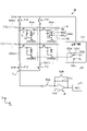
- FIG. 4 is a circuit diagram showing a plurality of partial detection areas. 4 also shows the circuit configuration of the detection circuit 48.
- the partial detection area PAA includes an optical sensor PD, a capacitive element Ca, and a first switching element Tr.
- the capacitive element Ca is a capacitor (sensor capacitor) formed in the photosensor PD, and equivalently electrically connected in parallel with the photosensor PD.
- FIG. 4 shows two gate lines GCL(m) and GCL(m+1) aligned in the second direction Dy among the plurality of gate lines GCL. Also, two signal lines SGL(n) and SGL(n+1) arranged in the first direction Dx among the plurality of signal lines SGL are shown.
- the partial detection area PAA is an area surrounded by the gate lines GCL and the signal lines SGL.
- the first switching element Tr is provided corresponding to the optical sensor PD.
- the first switching element Tr is composed of a thin film transistor, and in this example, is composed of an n-channel MOS (Metal Oxide Semiconductor) type TFT (Thin Film Transistor).
- MOS Metal Oxide Semiconductor
- TFT Thin Film Transistor
- the gates of the first switching elements Tr belonging to the plurality of partial detection areas PAA arranged in the first direction Dx are electrically connected to the gate line GCL.
- the sources of the first switching elements Tr belonging to the plurality of partial detection areas PAA arranged in the second direction Dy are electrically connected to the signal line SGL.
- the drain of the first switching element Tr is electrically connected to the first terminal N1 on the one end side of the optical sensor PD and the capacitive element Ca.
- the optical sensor PD has a first photodiode PDa and a second photodiode PDb.
- the first photodiode PDa and the second photodiode PDb are connected in series and in opposite directions between a first terminal N1 on one end side and a second terminal N2 on the other end side of the photosensor PD.
- “reversely connected” indicates a connection configuration in which the rectification characteristics of the first photodiode PDa and the second photodiode PDb are reversed.
- the cathode of the first photodiode PDa is electrically connected to the first terminal N1
- the anode of the first photodiode PDa is electrically connected to the anode of the second photodiode PDb
- the second photodiode PDb is electrically connected to the anode of the second photodiode PDb.
- a cathode of the photodiode PDb is electrically connected to the second terminal N2.
- a drive signal VDDSNS is supplied from the drive signal supply circuit 123a to the second terminal N2 (cathode of the second photodiode PDb) of the photosensor PD.
- the drive signal supply circuit 123 a is provided in the power supply circuit 123 . However, it is not limited to this, and the drive signal supply circuit 123 a may be provided in the control circuit 122 or may be provided on the sensor substrate 21 .
- the signal line SGL and the first terminal N1 are supplied from the power supply circuit 123 with a reference voltage that is the initial potential of the signal line SGL and the first terminal N1 (the capacitive element Ca and the optical sensor PD).
- a potential COM is supplied.
- a bias voltage VB is supplied to the photosensor PD by the drive signal VDDSNS and the reference potential COM.
- the drive signal supply circuit 123a that supplies the drive signal VDDSNS to the photosensor PD includes a first voltage signal supply section 123H, a second voltage signal supply section 123L, and a switch BSW.
- the first voltage signal supply section 123H is a circuit that supplies a first voltage signal VH having a higher level voltage than the reference potential COM.
- the second voltage signal supply section 123L is a circuit that supplies a second voltage signal VL having a voltage level lower than the reference potential COM.
- the switch BSW is a switching element that switches connection states between the first voltage signal supply section 123H and the second voltage signal supply section 123L, and the second terminal N2 of the optical sensor PD. By the operation of the switch BSW, the drive signal supply circuit 123a supplies the first voltage signal VH and the second voltage signal VL in a time division manner to the second terminal N2 of the photosensor PD.
- the first photodiode PDa When the first voltage signal VH (VH>COM) is supplied from the drive signal supply circuit 123a to the second terminal N2 of the photosensor PD, the first photodiode PDa is forward bias driven and the second photodiode PDb is reverse bias driven. Bias driven. In this case, the second photodiode PDb performs detection, and forward current flows through the first photodiode PDa.
- the reference potential COM is set to 0.75V and the first voltage signal VH is set to 2.75V.
- the first photodiode PDa When the second voltage signal VL (VL ⁇ COM) is supplied from the drive signal supply circuit 123a to the second terminal N2 of the photosensor PD, the first photodiode PDa is reverse bias driven, and the second photodiode PDb is driven forward. Bias driven. In this case, the first photodiode PDa performs detection, and forward current flows through the second photodiode PDb.
- the reference potential COM is set to 0.75V and the second voltage signal VL is set to -1.25V.
- the detection device 1 can detect a signal corresponding to the amount of light irradiated to the optical sensor PD for each partial detection area PAA or for each block unit PAG.
- the detection circuit 48 is electrically connected to the signal line SGL when the switch SSW is turned on during the readout period Pdet (see FIG. 7).
- the detection signal amplifying unit 42 of the detection circuit 48 converts the current fluctuation supplied from the signal line SGL into a voltage fluctuation and amplifies it.
- a reference potential (Vref) having a fixed potential is input to the non-inverting input section (+) of the detection signal amplifying section 42, and the signal line SGL is electrically connected to the inverting input terminal (-). .
- the same signal as the reference potential COM is input as the reference potential (Vref) voltage.
- the signal processing unit 44 (see FIG.
- the detection signal amplifying section 42 has a capacitive element Cb and a reset switch RSW. In the reset period Prst (see FIG. 7), the reset switch RSW is turned on to reset the charge of the capacitive element Cb.
- the optical sensor PD OPD: Organic Photo Diode
- FIG. 5 is a diagram showing an example of diode characteristics of an optical sensor.
- the horizontal axis indicates current and the vertical axis indicates voltage.
- the solid line shows the diode characteristics in the normal state
- the dashed line shows an example of the characteristic change due to the characteristic variation of the OPD.
- the reverse direction characteristics of the OPD may change as indicated by the dashed line.
- the reverse current flowing through the photosensor PD during an exposure period (effective exposure period), which will be described later, varies for each partial detection area PAA, and the detection accuracy decreases.
- the characteristics of the OPD are returned to the initial state (the solid line shown in FIG. 5) by passing a forward bias current through the photosensor PD at a predetermined timing.
- the operation of returning the OPD characteristics to the initial state is referred to as "refresh operation”.
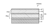
- FIG. 6 is a cross-sectional view showing a schematic cross-sectional configuration of the sensor section.
- the sensor section 10 includes a sensor substrate 21, a TFT layer 22, an insulating layer 23, an optical sensor PD, an intermediate layer 24, a sealing layer 25, and a protective layer 29.
- the sensor base material 21 is an insulating base material, and is made of, for example, glass or a resin material.
- the sensor substrate 21 is not limited to a flat plate shape, and may have a curved surface. In this case, the sensor substrate 21 may be a film-like resin.
- the sensor substrate 21 has a first surface S1 and a second surface S2 opposite to the first surface.
- a TFT layer 22, an insulating layer 23, an optical sensor PD, an intermediate layer 24, a sealing layer 25, and a protective layer 29 are laminated in this order on the first surface S1.
- a configuration will be described in which the light L1 is irradiated onto the optical sensor PD from the second surface S2 side.
- the configuration is not limited to this, and the light L1 may be irradiated to the optical sensor PD from the first surface S1 side.
- the TFT layer 22 is provided with circuits such as the gate line drive circuit 15 and the signal line selection circuit 16 described above. Further, the TFT layer 22 is provided with TFTs (Thin Film Transistors) such as the first switching element Tr, and various wirings such as gate lines GCL and signal lines SGL.
- TFTs Thin Film Transistors
- the sensor substrate 21 and the TFT layer 22 are driving circuit substrates for driving sensors in predetermined detection regions, and are also called backplanes or array substrates.
- the insulating layer 23 is an organic insulating layer and is provided on the TFT layer 22 .
- the insulating layer 23 is a flattening layer that flattens irregularities formed in the first switching element Tr formed in the TFT layer 22 and various conductive layers.
- the photosensor PD is provided on the insulating layer 23 .
- the first photodiode PDa and the second photodiode PDb are stacked in this order on the insulating layer 23 .
- the optical sensor PD includes a lower electrode 35 (first electrode), an electron transport layer 33, a first active layer 31a, and a hole transport layer in a direction perpendicular to the first surface S1 of the sensor substrate 21.
- 32, the second active layer 31b, and the upper electrode 34 (second electrode) are stacked in this order.
- the lower electrode 35 is provided on the insulating layer 23 and electrically connected to the first switching element Tr of the TFT layer 22 through a contact hole (not shown).
- the lower electrode 35 is the cathode (first terminal N1) of the first photodiode PDa, and is an electrode for reading out the detection signal Vdet.
- the lower electrode 35 is made of, for example, a translucent conductive material such as ITO (Indium Tin Oxide).
- the first active layer 31a and the second active layer 31b change their characteristics (for example, voltage-current characteristics and resistance value) according to the irradiated light.
- An organic material is used as the material of the first active layer 31a and the second active layer 31b.
- the first active layer 31a and the second active layer 31b are bulk heterostructures in which a p-type organic semiconductor and an n-type organic semiconductor, n-type fullerene derivative (PCBM) are mixed.
- C 60 fulllerene
- PCBM phenyl C61 butyric acid methyl ester: [6,6]-Phenyl C61 butyric acid methyl ester
- CuPc copper phthalocyanine
- F 16 CuPc fluorinated copper phthalocyanine
- rubrene 5,6,11,12-tetraphenyltetracene
- PDI perylene derivative
- the first active layer 31a and the second active layer 31b can be formed by vapor deposition (dry process) using these low-molecular-weight organic materials.
- the first active layer 31a and the second active layer 31b may be, for example, a laminated film of CuPc and F16CuPc or a laminated film of rubrene and C60.
- the first active layer 31a and the second active layer 31b can also be formed by a wet process.
- the first active layer 31a and the second active layer 31b are made of a combination of the above-described low-molecular-weight organic material and high-molecular-weight organic material.
- the first active layer 31a and the second active layer 31b can be a mixed film of P3HT and PCBM or a mixed film of F8BT and PDI.
- the first active layer 31a and the second active layer 31b may be made of the same material or may be made of different materials.
- P3HT:PCMB a film in which P3HT and PCBM are mixed
- PMDPP3T poly[[2,5-bis(2-hexyldecyl)-2,3,5,6-tetrahydro-3,6-dioxopyrrolo[3,4-c]pyrrole-1, 4-diyl]-alt-[3′,3′′-dimethyl-2,2′:5′,2′′-terthiophene]-5,5′′-diyl]
- PCBM [6,6]- Phenyl C61 butyric acid methyl ester) (film in which PMDPP3T and PCBM are mixed) can be used.
- the first photodiode PDa has sensitivity to visible light (for example, wavelengths of 400 nm to 650 nm).
- the second photodiode PDb has sensitivity to near-infrared light (for example, wavelengths of 780 nm to 950 nm).
- the upper electrode 34 is the cathode (second terminal N2) of the second photodiode PDb, and is an electrode for supplying the drive signal VDDSNS to the photosensor PD.
- the upper electrode 34 and the lower electrode 35 face each other with the first active layer 31a and the second active layer 31b interposed therebetween.
- Aluminum (Al) for example, is used for the upper electrode 34 .
- the upper electrode 34 may be a metal material such as silver (Ag), or an alloy material containing at least one of these metal materials.
- the electron transport layer 33 and the hole transport layer 32 are provided to facilitate the holes and electrons generated in the first active layer 31 a and the second active layer 31 b to reach the upper electrode 34 or the lower electrode 35 .
- the electron transport layer 33 is provided between the lower electrode 35 and the first active layer 31a in a direction perpendicular to the first surface S1 of the sensor substrate 21 .
- the electron transport layer 33 is directly on the lower electrode 35 and the first active layer 31 a is directly on the electron transport layer 33 .
- Ethoxylated polyethyleneimine (PEIE) or zinc oxide (ZnO) is used as the material of the electron transport layer 33 .
- the hole transport layer 32 is provided between the first active layer 31a and the second active layer 31b in a direction perpendicular to the first surface S1 of the sensor substrate 21.
- the hole transport layer 32 is directly on the first active layer 31 a and the second active layer 31 b is directly on the hole transport layer 32 .
- a polythiophene-based conductive polymer (PEDOT (poly(3,4-ethylenedioxythiophene)): PSS (poly(styrene sulfonate))) is used for the hole transport layer 32 .
- the hole transport layer 32 is shared by the first photodiode PDa and the second photodiode PDb.
- a sealing layer 25 is provided to cover the photosensor PD. More specifically, the sealing layer 25 is provided on the upper electrode 34 with the intermediate layer 24 interposed therebetween.
- the material of the sealing layer 25 is aluminum oxide (Al 2 O 3 ).
- the detection device 1 can seal the photosensor PD better than when parylene is used as the sealing layer 25 .
- ITO is used as the material of the intermediate layer 24 , and the intermediate layer 24 can improve adhesion between the upper electrode 34 and the sealing layer 25 .
- a protective layer 29 is provided to cover the sealing layer 25 .
- a resin film for example, is used for the protective layer 29 .
- a protective layer 29 is provided to protect the optical sensor PD.
- the material of the protective layer 29 is not limited to the resin film, and other materials may be used.
- the configuration in which the light L1 is irradiated to the optical sensor PD from the second surface S2 side has been described, but the configuration may be such that the light L1 is irradiated to the optical sensor PD from the first surface S1 side.
- a conductive material having translucency such as ITO is used as the upper electrode 34 and a metal material such as aluminum or silver is used as the lower electrode 35 .
- FIG. 7 is a timing waveform diagram showing an operation example of the detection device.
- FIG. 7 shows the operation when the second voltage signal VL is mainly supplied as the drive signal VDDSNS, that is, when the first photodiode PDa of the photosensor PD detects.
- the description of FIG. 7 can also be applied to the case where the first voltage signal VH is supplied as the drive signal VDDSNS, that is, detection by the second photodiode PDb of the photosensor PD.
- the detection device 1 has a reset period Prst, an exposure period Pex, and a readout period Pdet.
- the power supply circuit 123 (drive signal supply circuit 123a) supplies the drive signal VDDSNS to the anode of the photosensor PD over the reset period Prst, the exposure period Pex, and the readout period Pdet.
- the drive signal VDDSNS is a signal that applies a bias voltage VB between the first terminal N1 and the second terminal N2 of the photosensor PD.
- the reference potential COM of substantially 0.75 V is applied to the first terminal N1 of the photosensor PD.
- a bias voltage VB of substantially 2.0V is supplied between the -second terminals N2.
- the control circuit 122 After setting the reset signal RST2 to "H", the control circuit 122 supplies the start signal STV and the clock signal CK to the gate line driving circuit 15, and the reset period Prst starts. In the reset period Prst, the control circuit 122 supplies the reference potential COM to the reset circuit 17, and turns on the fourth switching element TrR for supplying the reset voltage by the reset signal RST2. As a result, each signal line SGL is supplied with the reference potential COM as a reset voltage.
- the gate line drive circuit 15 sequentially selects the gate lines GCL based on the start signal STV, clock signal CK, and reset signal RST1.
- the gate line driving circuit 15 sequentially supplies gate driving signals Vgcl ⁇ Vgcl(1) to Vgcl(M) ⁇ to the gate lines GCL.
- the gate drive signal Vgcl has a pulse-like waveform having a high-level power supply voltage VDD and a low-level power supply voltage VSS.
- gate lines GCL are provided, and gate drive signals Vgcl(1), .
- One switching element Tr is sequentially turned on for each row, and a reset voltage is supplied. For example, a reference potential COM of 0.75 V is supplied as the reset voltage.
- the capacitive elements Ca in all the partial detection areas PAA are electrically connected to the signal line SGL in sequence and supplied with the reference potential COM.
- the capacitance of the capacitive element Ca is reset.
- Examples of exposure timing include a gate line non-selected exposure control method and a constant exposure control method.
- gate line non-selected exposure control method gate drive signals ⁇ Vgcl(1) to (M) ⁇ are sequentially supplied to all gate lines GCL electrically connected to the photosensor PD to be detected, A reset voltage is supplied to all the photosensors PD. After that, when all the gate lines GCL electrically connected to the photosensor PD to be detected become low voltage (the first switching element Tr is turned off), exposure is started, and exposure is performed during the exposure period Pex.
- the gate drive signals ⁇ Vgcl(1) to (M) ⁇ are sequentially supplied to the gate lines GCL electrically connected to the photosensor PD to be detected as described above, and the readout is performed during the readout period Pdet.
- the effective exposure period SPex(1) starts immediately after the gate drive signal Vgcl(1) is supplied to the gate line GCL during the reset period Prst.
- the effective exposure period SPex ⁇ (1) . . . (M) ⁇ is a period during which the photosensor PD charges the capacitive element Ca.
- the effective exposure period SPex is started when the first switching element Tr is turned off.
- the charge charged in the capacitive element Ca during the reset period Prst flows as a reverse current (from the cathode to the anode) into the photosensor PD due to light irradiation, and the potential difference of the capacitive element Ca decreases.
- the effective exposure periods SPex(1), . . . , SPex(M) have the same exposure time length.
- the control circuit 122 sets the reset signal RST2 to a low level voltage. This stops the operation of the reset circuit 17 .
- the reset signal may be a high level voltage only during the reset period Prst.
- the gate line drive circuit 15 sequentially supplies the gate drive signals Vgcl(1), . . . , Vgcl(M) to the gate lines GCL.
- the gate line drive circuit 15 supplies the gate drive signal Vgcl(1) of the high level voltage (power supply voltage VDD) to the gate line GCL(1) in the period V(1).
- the control circuit 122 sequentially supplies the selection signals ASW1, .
- the signal lines SGL of the partial detection areas PAA selected by the gate drive signal Vgcl(1) are electrically connected to the detection circuit 48 sequentially or simultaneously.
- the detection signal Vdet is supplied to the detection circuit 48 for each partial detection area PAA.
- the gate line driving circuit 15 drives the gate lines GCL(2), . . . , GCL(M ⁇ 1), GCL(M ) are supplied with high level voltage gate drive signals Vgcl(2), . . . , Vgcl(M ⁇ 1), Vgcl(M). That is, the gate line drive circuit 15 supplies the gate drive signal Vgcl to the gate line GCL every period V(1), V(2), . . . , V(M ⁇ 1), V(M).
- the signal line selection circuit 16 sequentially selects the signal lines SGL based on the selection signal ASW each time the gate drive signal Vgcl is at a high level voltage.
- the signal line selection circuit 16 is electrically connected to one detection circuit 48 in sequence for each signal line SGL. Thereby, the detection device 1 can output the detection signals Vdet of all the partial detection areas PAA to the detection circuit 48 during the readout period Pdet.
- FIG. 8 is a timing waveform diagram showing an operation example during the readout period in FIG. An operation example in the supply period Readout of one gate drive signal Vgcl(j) in FIG. 7 will be described below with reference to FIG. In FIG. 7, the first gate drive signal Vgcl(1) is labeled with the supply period Readout, but the other gate drive signals Vgcl(2), . . . , Vgcl(M) are the same. j is any natural number from 1 to M;
- the output voltage (V out ) of the third switching element TrS is previously reset to the reference potential (Vref) voltage.
- a reference potential (Vref) voltage is a reset voltage, for example, 0.75V.
- the gate drive signal Vgcl(j) becomes high level to turn on the first switching element Tr of the row, and the signal line SGL of each row is turned on according to the charge accumulated in the capacitance (capacitive element Ca) of the partial detection area PAA. voltage.
- the period t1 elapses from the rise of the gate drive signal Vgcl(j), there occurs a period t2 in which the selection signal ASW(k) is high.
- the switch SSW is turned on (the high level period t4 of the SSW signal)
- the charge accumulated in the capacitance (capacitance element Ca) of the partial detection area PAA is transferred to the capacitance (capacitance element Cb) of the detection signal amplifying section 42 of the detection circuit 48.
- the output voltage of the detection signal amplifier 42 becomes a voltage corresponding to the charge accumulated in the capacitive element Cb.
- the inverting input portion of the detection signal amplifying portion 42 is at the imaginary short potential of the operational amplifier, so that it returns to the reference potential (Vref).
- the output voltage of the detection signal amplifier 42 is read out by the A/D converter 43 .
- ASW(k), ASW(k+1), . . . in FIG. 8 are, for example, any one of ASW1 to ASW6 in FIG.
- the voltage of the capacitive element Cb becomes a voltage corresponding to the charge accumulated in the capacitance (capacitive element Ca) of the partial detection area PAA at the portion where the third switching element TrS is turned on according to the selection signal ASW(k). .
- the output voltage (V out ) of the third switching element TrS becomes the reference potential (Vref) voltage due to an imaginary short
- the output voltage of the detection signal amplifier 42 becomes a voltage corresponding to the capacitance of the capacitive element Cb.
- the output voltage is read by the A/D converter 43 .
- the voltage of the capacitive element Cb is, for example, the voltage between two electrodes provided in the capacitor that constitutes the capacitive element Cb.
- the period t1 is, for example, 20 [ ⁇ s].
- the period t2 is, for example, 60 [ ⁇ s].
- the period t3 is, for example, 44.7 [ ⁇ s].
- the period t4 is, for example, 0.98 [ ⁇ s].
- the gate line drive circuit 15 selects the gate lines GCL individually, but the present invention is not limited to this.
- the gate line drive circuit 15 may simultaneously select a predetermined number of gate lines GCL, which is two or more, and sequentially supply the gate drive signal Vgcl to each of the predetermined number of gate lines GCL.
- the signal line selection circuit 16 may also electrically connect a predetermined number of signal lines SGL, which is two or more, to one detection circuit 48 at the same time.
- the gate line driving circuit 15 may scan a plurality of gate lines GCL by thinning them out.
- FIG. 9 is a graph schematically showing the relationship between bias voltage and detected value.
- FIG. 9 shows the relationship between the bias voltage VB and the detected value for each of the first photodiode PDa and the second photodiode PDb of the photosensor PD.
- the horizontal axis of the graph shown in FIG. 9 represents the bias voltage VB supplied to the optical sensor PD, and the vertical axis represents the detected value from the optical sensor PD.
- the detected value is a voltage signal output from the detection circuit 48 .
- the detected value may be the output voltage (V out ) of the third switching element TrS shown in FIG.
- the first photodiode PDa detects visible light (wavelength 400 nm or more and 650 nm or less, for example 525 nm), and the second photodiode PDb detects near-infrared light (wavelength 780 nm or more and 950 nm or less, for example 850 nm). A case of detection will be described.
- the first photodiode PDa is forward bias driven and the second photodiode PDb is reverse bias driven. Thereby, the current flowing through the second photodiode PDb is detected. Therefore, when the bias voltage VB has a negative polarity, the photosensor PD is mainly sensitive to near-infrared light.
- the second photodiode PDb has sensitivity to visible light in addition to near-infrared light. Therefore, as shown in FIG. 9, when the bias voltage VB has a negative polarity, the photosensor PD has sensitivity to near-infrared light and visible light.
- the first photodiode PDa When the bias voltage VB has a positive polarity, the first photodiode PDa is reverse bias driven and the second photodiode PDb is forward bias driven. Thereby, the current flowing through the first photodiode PDa is detected. Therefore, when the bias voltage VB is of positive polarity, the photosensor PD is primarily sensitive to visible light.
- the detection device 1 can change the wavelength region of the light L1 to which the photosensor PD is sensitive by switching the polarity of the bias voltage VB.
- the detection device 1 can have detection sensitivity in a different wavelength region than when the optical sensor PD is formed of either the first photodiode PDa or the second photodiode PDb.
- the detection device 1 can have detection sensitivity in a different wavelength region than when the optical sensor PD is formed of either the first photodiode PDa or the second photodiode PDb.
- the detection device 1 can change the wavelength region of the light L1 to which the photosensor PD is sensitive by switching the polarity of the bias voltage VB.
- the detection device 1 can have detection sensitivity in a different wavelength region than when the optical sensor PD is formed of either the first photodiode PDa or the second photodiode PDb.
- the sensitivity can be set to two different wavelengths, it is possible to obtain blood oxygen saturation measurement, which requires information at different wavelength
- the wavelength region having sensitivity is not limited to this.
- the first photodiode PDa and the second photodiode PDb have sensitivities in different regions of the visible region
- the first photodiode PDa and the second photodiode PDb have sensitivities in different regions of the infrared region
- the first photodiode PDa And/or a case where the second photodiode PDb has sensitivity in the ultraviolet wavelength range is also included in the present invention.
- first photodiode PDa and the second photodiode PDb are not limited to biosensors, and can be applied to color scanners, color image detection devices, and the like.
- three pixels with different sensitivities of RGB were required to detect a color image
- only two pixels are required. That is, one of the two pixels is sensitive to two wavelength regions and the other pixel is sensitive to one or two wavelength regions.
- two pixels may be sensitized in three or four wavelength regions.
- FIG. 10 is an explanatory diagram for explaining an example of the driving method of the detection device.
- the period Tm is a period during which the drive signal supply circuit 123a (see FIG. 4) supplies the second voltage signal VL to the second terminal N2 of the photosensor PD through the operation of the switch BSW.
- the period Tp is a period during which the drive signal supply circuit 123a (see FIG. 4) supplies the first voltage signal VH to the second terminal N2 of the photosensor PD by the operation of the switch BSW.
- the driving signal supply circuit 123a supplies the first voltage signal VH and the second voltage signal VL to the photosensor PD in a time-division manner, so that the polarity of the bias voltage VB alternates between the period Tm and the period Tp. flip to
- the first photodiode PDa is refreshed in period Tp and performs detection in period Tm.
- the second photodiode PDb performs detection during the period Tp and is refreshed during the period Tm.
- a detection period and a refresh period are alternately arranged. Therefore, the optical sensor PD can suppress changes in detection sensitivity over time.
- the optical sensor PD can suppress a decrease in detection speed.
- the period Tm and the period Tp may be arranged in any way.
- the period Tm and the period Tp are alternately arranged for each detection frame period in which the gate line driving circuit 15 scans all the gate lines GCL (gate line GCL(1) to gate line GCL(M)).
- the period Tm and the period Tp may be arranged in one detection frame period.
- the period Tm and the period Tp may be alternately arranged for every plurality of detection frames.
- the first photodiode PDa and the second photodiode PDb detect light of different wavelengths, for example, the first photodiode PDa detects visible light and the second photodiode PDb detects near-infrared light, as described above.
- the first light source 61 and the second light source 62 (see FIG. 1) for irradiation may be turned on and off every period Tm and period Tp.
- the first photodiode PDa detects visible light and the second photodiode PDb detects near-infrared light.
- the diode PDb may be configured to detect visible light.
- the first photodiode PDa and the second photodiode PDb may be configured to detect light in the same wavelength range.
- the detection device 1 of the present embodiment is a detection device 1 having a plurality of optical sensors PD arranged on a substrate (sensor substrate 21). , a first photodiode PDa, and a second photodiode PDb connected in series and in the opposite direction to the first photodiode PDa.
- the detection device 1 suppresses a decrease in the detection speed while suppressing changes in the sensitivity characteristic over time. can be suppressed.
- FIG. 11 is a circuit diagram showing part of the partial detection area according to the modification.
- the detection device 1A of the modified example differs from the above-described first embodiment in the connection configuration between the first photodiode PDa and the second photodiode PDb.
- the cathode of the second photodiode PDb is electrically connected to the first terminal N1
- the anode of the first photodiode PDa is electrically connected to the anode of the second photodiode PDb
- the first photodiode PDb is electrically connected to the anode of the second photodiode PDb.
- a cathode of the diode PDa is electrically connected to the second terminal N2.
- FIG. 12 is a cross-sectional view showing a schematic cross-sectional configuration of an optical sensor according to a modification.
- the sensor unit 10 according to the modification includes a sensor substrate 21 and an optical sensor PD.
- the sensor substrate 21 is a glass substrate.
- the optical sensor PD is provided on the sensor substrate 21 .
- the first photodiode PDa and the second photodiode PDb are laminated on the sensor substrate 21 in this order.
- the optical sensor PD includes a lower electrode 35 (first electrode), an electron transport layer 33, a first active layer 31a, a hole transport layer 32, and a second active layer 31b on the sensor substrate 21.
- the upper electrode 34 second electrode
- the lower electrode 35 is made of a translucent conductive material such as ITO (Indium Tin Oxide). Zinc oxide (ZnO) is used as the material of the electron transport layer 33 .
- the first active layer 31a is P3HT (poly(3-hexylthiophene)):PCMB ([6,6]-phenyl C61 butyric acid methyl ester).
- P3HT is a P-type semiconductor
- PCBM is an N-type semiconductor
- P3HT:PCMB is a heterojunction OPD in which P3HT and PCMB are mixed.
- a polythiophene-based conductive polymer (PEDOT (poly (3,4-ethylenedioxythiophene)): PSS (poly (styrene sulfonate)) is used for the hole transport layer 32 .
- PEDOT poly (3,4-ethylenedioxythiophene)
- PSS poly (styrene sulfonate)
- the second active layer 31b is composed of PMDPP3T (poly[[2,5-bis(2-hexyldecyl)-2,3,5,6-tetrahydro-3,6-dioxopyrrolo[3,4-c]pyrrole-1,4 -diyl]-alt-[3′,3′′-dimethyl-2,2′:5′,2′′-terthiophene]-5,5′′-diyl]): PCBM ([6,6]-Phenyl C61 butyric acid methyl ester).
- PMDPP3T is a P-type semiconductor
- PCBM is an N-type semiconductor
- PMDPP3T:PCMB is a heterojunction OPD in which PMDPP3T and PCMB are mixed.
- aluminum (Al) is used for the upper electrode 34 .
- FIG. 13 is a graph schematically showing wavelength sensitivity characteristics of the optical sensor according to the modification.
- the bias voltage VB has a negative polarity
- the first photodiode PDa is reverse bias driven and the second photodiode PDb is forward bias driven.
- the current flowing through the first photodiode PDa is detected. Therefore, when the bias voltage VB is of negative polarity, the photosensor PD is primarily sensitive to visible light.
- the second photodiode PDb When the bias voltage VB has a positive polarity, the second photodiode PDb is reverse bias driven and the first photodiode PDa is forward bias driven. Thereby, the current flowing through the second photodiode PDb is detected. Therefore, when the bias voltage VB has a positive polarity, the photosensor PD is mainly sensitive to near-infrared light.
- FIG. 14 is a circuit diagram showing a detection device according to the second embodiment.
- the same components as those described in the above-described embodiment are denoted by the same reference numerals, and overlapping descriptions are omitted.
- the detection device 1B of the second embodiment differs from the above-described first embodiment in the connection configuration of the optical sensor PDA. Specifically, the anode of the first photodiode PDa is electrically connected to the second terminal N2, the cathode of the first photodiode PDa is electrically connected to the cathode of the second photodiode PDb, and the second photodiode PDa is electrically connected to the cathode of the second photodiode PDb.
- the anode of diode PDb is electrically connected to first terminal N1.
- the first photodiode PDa and the second photodiode PDb are connected in series and in reverse between the first terminal N1 on one end side and the second terminal N2 on the other end side of the photosensor PDA. direction is connected.
- the rectification characteristics of each of the first photodiode PDa and the second photodiode PDb are inverted with respect to the configuration of the first embodiment. Therefore, when the bias voltage VB of ⁇ 2.0 V is supplied to the photosensor PDA (for example, period Tm in FIG. 10), the first photodiode PDa is forward-bias driven (refreshed), and the second photodiode PDb is driven (refreshed). is driven (detected) in reverse bias. Further, when the bias voltage VB of +2.0 V is supplied to the photosensor PDA (for example, period Tp in FIG. 10), the first photodiode PDa is reverse bias driven (detected), and the second photodiode PDb is forward biased. Bias driven (refreshed).
- Reference Signs List 1 1A, 1B detection device 10 sensor unit 11 detection control unit 15 gate line drive circuit 16 signal line selection circuit 21 sensor substrate 31a first active layer 31b second active layer 32 hole transport layer 33 electron transport layer 34 upper electrode 35 lower electrode 40 detection unit 48 detection circuit 123a drive signal supply circuit N1 first terminal N2 second terminal PD optical sensor PDa first photodiode PDb second photodiode VDDSNS drive signal COM reference potential VB bias voltage VH first voltage signal VL Second voltage signal
Landscapes
- Physics & Mathematics (AREA)
- Engineering & Computer Science (AREA)
- Power Engineering (AREA)
- Health & Medical Sciences (AREA)
- Life Sciences & Earth Sciences (AREA)
- Electromagnetism (AREA)
- Microelectronics & Electronic Packaging (AREA)
- Computer Hardware Design (AREA)
- General Physics & Mathematics (AREA)
- Condensed Matter Physics & Semiconductors (AREA)
- Biomedical Technology (AREA)
- Surgery (AREA)
- General Health & Medical Sciences (AREA)
- Public Health (AREA)
- Veterinary Medicine (AREA)
- Biophysics (AREA)
- Pathology (AREA)
- Animal Behavior & Ethology (AREA)
- Molecular Biology (AREA)
- Medical Informatics (AREA)
- Heart & Thoracic Surgery (AREA)
- Optics & Photonics (AREA)
- Spectroscopy & Molecular Physics (AREA)
- Multimedia (AREA)
- Signal Processing (AREA)
- Solid State Image Pick-Up Elements (AREA)
Abstract
Description
図1は、第1実施形態に係る検出装置を示す平面図である。図1に示すように、検出装置1は、センサ基材21と、センサ部10と、ゲート線駆動回路15と、信号線選択回路16と、検出回路48と、制御回路122と、電源回路123と、第1光源基材51と、第2光源基材52と、第1光源61と、第2光源62と、を有する。第1光源基材51には、複数の第1光源61が設けられる。第2光源基材52には複数の第2光源62が設けられる。
図14は、第2実施形態に係る検出装置を示す回路図である。なお、以下の説明では、上述した実施形態で説明したものと同じ構成要素には同一の符号を付して重複する説明は省略する。
10 センサ部
11 検出制御部
15 ゲート線駆動回路
16 信号線選択回路
21 センサ基材
31a 第1活性層
31b 第2活性層
32 正孔輸送層
33 電子輸送層
34 上部電極
35 下部電極
40 検出部
48 検出回路
123a 駆動信号供給回路
N1 第1端子
N2 第2端子
PD 光センサ
PDa 第1フォトダイオード
PDb 第2フォトダイオード
VDDSNS 駆動信号
COM 基準電位
VB バイアス電圧
VH 第1電圧信号
VL 第2電圧信号
Claims (6)
- 基板の上に配列された複数の光センサを有する検出装置であって、
複数の前記光センサは、それぞれ、
第1フォトダイオードと、
前記第1フォトダイオードと直列に、かつ、逆方向に接続される第2フォトダイオードと、を有する
検出装置。 - 前記第1フォトダイオードと前記第2フォトダイオードは、光の波長に対して異なる感度特性を有する
請求項1に記載の検出装置。 - 前記第1フォトダイオードは、可視光を検出し、
前記第2フォトダイオードは、近赤外光を検出する
請求項1又は請求項2に記載の検出装置。 - 前記光センサに駆動信号を供給する駆動信号供給回路を有し、
前記駆動信号供給回路は、基準電位よりも高レベル電圧の第1電圧信号と、前記基準電位よりも低レベル電圧の第2電圧信号と、を時分割で前記光センサに供給する
請求項1から請求項3のいずれか1項に記載の検出装置。 - 前記第1フォトダイオードが順バイアス駆動され、前記第2フォトダイオードが逆バイアス駆動された場合に、前記第2フォトダイオードが検出し、
前記第1フォトダイオードが逆バイアス駆動され、前記第2フォトダイオードが順バイアス駆動された場合に、前記第1フォトダイオードが検出する
請求項1から請求項4のいずれか1項に記載の検出装置。 - 前記光センサは、前記基板に垂直な方向で、第1電極、電子輸送層、第1活性層、正孔輸送層、第2活性層、第2電極の順に積層される
請求項1から請求項5のいずれか1項に記載の検出装置。
Priority Applications (3)
| Application Number | Priority Date | Filing Date | Title |
|---|---|---|---|
| JP2022578436A JPWO2022163681A1 (ja) | 2021-01-26 | 2022-01-26 | |
| CN202280011674.4A CN116783711A (zh) | 2021-01-26 | 2022-01-26 | 检测装置 |
| US18/225,809 US20230369355A1 (en) | 2021-01-26 | 2023-07-25 | Detection device |
Applications Claiming Priority (2)
| Application Number | Priority Date | Filing Date | Title |
|---|---|---|---|
| JP2021010589 | 2021-01-26 | ||
| JP2021-010589 | 2021-01-26 |
Related Child Applications (1)
| Application Number | Title | Priority Date | Filing Date |
|---|---|---|---|
| US18/225,809 Continuation US20230369355A1 (en) | 2021-01-26 | 2023-07-25 | Detection device |
Publications (1)
| Publication Number | Publication Date |
|---|---|
| WO2022163681A1 true WO2022163681A1 (ja) | 2022-08-04 |
Family
ID=82653573
Family Applications (1)
| Application Number | Title | Priority Date | Filing Date |
|---|---|---|---|
| PCT/JP2022/002773 WO2022163681A1 (ja) | 2021-01-26 | 2022-01-26 | 検出装置 |
Country Status (4)
| Country | Link |
|---|---|
| US (1) | US20230369355A1 (ja) |
| JP (1) | JPWO2022163681A1 (ja) |
| CN (1) | CN116783711A (ja) |
| WO (1) | WO2022163681A1 (ja) |
Citations (3)
| Publication number | Priority date | Publication date | Assignee | Title |
|---|---|---|---|---|
| DE102011081564A1 (de) * | 2011-08-25 | 2013-02-28 | Ifm Electronic Gmbh | Empfänger für einen optischen Entfernungsmesser |
| US20150129747A1 (en) * | 2013-11-12 | 2015-05-14 | Intrinsix Corporation | Stacked photodiode multispectral imager |
| JP2018116108A (ja) * | 2017-01-17 | 2018-07-26 | 株式会社ジャパンディスプレイ | 表示装置 |
Family Cites Families (1)
| Publication number | Priority date | Publication date | Assignee | Title |
|---|---|---|---|---|
| CN110323235A (zh) * | 2018-03-29 | 2019-10-11 | 夏普株式会社 | 摄像面板 |
-
2022
- 2022-01-26 CN CN202280011674.4A patent/CN116783711A/zh active Pending
- 2022-01-26 JP JP2022578436A patent/JPWO2022163681A1/ja active Pending
- 2022-01-26 WO PCT/JP2022/002773 patent/WO2022163681A1/ja active Application Filing
-
2023
- 2023-07-25 US US18/225,809 patent/US20230369355A1/en active Pending
Patent Citations (3)
| Publication number | Priority date | Publication date | Assignee | Title |
|---|---|---|---|---|
| DE102011081564A1 (de) * | 2011-08-25 | 2013-02-28 | Ifm Electronic Gmbh | Empfänger für einen optischen Entfernungsmesser |
| US20150129747A1 (en) * | 2013-11-12 | 2015-05-14 | Intrinsix Corporation | Stacked photodiode multispectral imager |
| JP2018116108A (ja) * | 2017-01-17 | 2018-07-26 | 株式会社ジャパンディスプレイ | 表示装置 |
Also Published As
| Publication number | Publication date |
|---|---|
| CN116783711A (zh) | 2023-09-19 |
| US20230369355A1 (en) | 2023-11-16 |
| JPWO2022163681A1 (ja) | 2022-08-04 |
Similar Documents
| Publication | Publication Date | Title |
|---|---|---|
| US11888080B2 (en) | Detection device including light sources along an outer circumference of two detection areas each of the detection areas having a specific scan direction | |
| US20230165019A1 (en) | Detection device | |
| JP2024026475A (ja) | 検出装置、指紋検出装置及び静脈検出装置 | |
| US20220328564A1 (en) | Detection device and imaging device | |
| US11604543B2 (en) | Detection device | |
| WO2022163681A1 (ja) | 検出装置 | |
| WO2021049262A1 (ja) | 検出装置 | |
| WO2023149195A1 (ja) | 検出装置 | |
| WO2022168828A1 (ja) | 検出装置 | |
| US20230134613A1 (en) | Detection device | |
| US11645825B2 (en) | Detection device | |
| US20220338352A1 (en) | Detection device | |
| WO2022220287A1 (ja) | 検出装置 | |
| WO2023032863A1 (ja) | 検出装置 | |
| US20230055390A1 (en) | Detection device | |
| JP2023028058A (ja) | 検出システム | |
| JP2022190538A (ja) | 検出装置 | |
| JP2023030471A (ja) | 検出装置 | |
| JP2023012379A (ja) | 検出装置 |
Legal Events
| Date | Code | Title | Description |
|---|---|---|---|
| 121 | Ep: the epo has been informed by wipo that ep was designated in this application |
Ref document number: 22745901 Country of ref document: EP Kind code of ref document: A1 |
|
| ENP | Entry into the national phase |
Ref document number: 2022578436 Country of ref document: JP Kind code of ref document: A |
|
| WWE | Wipo information: entry into national phase |
Ref document number: 202280011674.4 Country of ref document: CN |
|
| NENP | Non-entry into the national phase |
Ref country code: DE |
|
| 122 | Ep: pct application non-entry in european phase |
Ref document number: 22745901 Country of ref document: EP Kind code of ref document: A1 |