WO2022158388A1 - 電源システム装置 - Google Patents
電源システム装置 Download PDFInfo
- Publication number
- WO2022158388A1 WO2022158388A1 PCT/JP2022/001131 JP2022001131W WO2022158388A1 WO 2022158388 A1 WO2022158388 A1 WO 2022158388A1 JP 2022001131 W JP2022001131 W JP 2022001131W WO 2022158388 A1 WO2022158388 A1 WO 2022158388A1
- Authority
- WO
- WIPO (PCT)
- Prior art keywords
- power conversion
- control
- signal
- common
- unit
- Prior art date
- Legal status (The legal status is an assumption and is not a legal conclusion. Google has not performed a legal analysis and makes no representation as to the accuracy of the status listed.)
- Ceased
Links
Images





Classifications
-
- H—ELECTRICITY
- H02—GENERATION; CONVERSION OR DISTRIBUTION OF ELECTRIC POWER
- H02M—APPARATUS FOR CONVERSION BETWEEN AC AND AC, BETWEEN AC AND DC, OR BETWEEN DC AND DC, AND FOR USE WITH MAINS OR SIMILAR POWER SUPPLY SYSTEMS; CONVERSION OF DC OR AC INPUT POWER INTO SURGE OUTPUT POWER; CONTROL OR REGULATION THEREOF
- H02M3/00—Conversion of DC power input into DC power output
- H02M3/02—Conversion of DC power input into DC power output without intermediate conversion into AC
- H02M3/04—Conversion of DC power input into DC power output without intermediate conversion into AC by static converters
- H02M3/10—Conversion of DC power input into DC power output without intermediate conversion into AC by static converters using discharge tubes with control electrode or semiconductor devices with control electrode
- H02M3/145—Conversion of DC power input into DC power output without intermediate conversion into AC by static converters using discharge tubes with control electrode or semiconductor devices with control electrode using devices of a triode or transistor type requiring continuous application of a control signal
- H02M3/155—Conversion of DC power input into DC power output without intermediate conversion into AC by static converters using discharge tubes with control electrode or semiconductor devices with control electrode using devices of a triode or transistor type requiring continuous application of a control signal using semiconductor devices only
- H02M3/156—Conversion of DC power input into DC power output without intermediate conversion into AC by static converters using discharge tubes with control electrode or semiconductor devices with control electrode using devices of a triode or transistor type requiring continuous application of a control signal using semiconductor devices only with automatic control of output voltage or current, e.g. switching regulators
- H02M3/158—Conversion of DC power input into DC power output without intermediate conversion into AC by static converters using discharge tubes with control electrode or semiconductor devices with control electrode using devices of a triode or transistor type requiring continuous application of a control signal using semiconductor devices only with automatic control of output voltage or current, e.g. switching regulators including plural semiconductor devices as final control devices for a single load
- H02M3/1584—Conversion of DC power input into DC power output without intermediate conversion into AC by static converters using discharge tubes with control electrode or semiconductor devices with control electrode using devices of a triode or transistor type requiring continuous application of a control signal using semiconductor devices only with automatic control of output voltage or current, e.g. switching regulators including plural semiconductor devices as final control devices for a single load with a plurality of power processing stages connected in parallel
-
- H—ELECTRICITY
- H02—GENERATION; CONVERSION OR DISTRIBUTION OF ELECTRIC POWER
- H02M—APPARATUS FOR CONVERSION BETWEEN AC AND AC, BETWEEN AC AND DC, OR BETWEEN DC AND DC, AND FOR USE WITH MAINS OR SIMILAR POWER SUPPLY SYSTEMS; CONVERSION OF DC OR AC INPUT POWER INTO SURGE OUTPUT POWER; CONTROL OR REGULATION THEREOF
- H02M1/00—Details of apparatus for conversion
- H02M1/0003—Details of control, feedback or regulation circuits
- H02M1/0009—Devices or circuits for detecting current in a converter
-
- H—ELECTRICITY
- H02—GENERATION; CONVERSION OR DISTRIBUTION OF ELECTRIC POWER
- H02M—APPARATUS FOR CONVERSION BETWEEN AC AND AC, BETWEEN AC AND DC, OR BETWEEN DC AND DC, AND FOR USE WITH MAINS OR SIMILAR POWER SUPPLY SYSTEMS; CONVERSION OF DC OR AC INPUT POWER INTO SURGE OUTPUT POWER; CONTROL OR REGULATION THEREOF
- H02M1/00—Details of apparatus for conversion
- H02M1/0003—Details of control, feedback or regulation circuits
- H02M1/0025—Arrangements for modifying reference values, feedback values or error values in the control loop of a converter
-
- H—ELECTRICITY
- H02—GENERATION; CONVERSION OR DISTRIBUTION OF ELECTRIC POWER
- H02M—APPARATUS FOR CONVERSION BETWEEN AC AND AC, BETWEEN AC AND DC, OR BETWEEN DC AND DC, AND FOR USE WITH MAINS OR SIMILAR POWER SUPPLY SYSTEMS; CONVERSION OF DC OR AC INPUT POWER INTO SURGE OUTPUT POWER; CONTROL OR REGULATION THEREOF
- H02M1/00—Details of apparatus for conversion
- H02M1/08—Circuits specially adapted for the generation of control voltages for semiconductor devices incorporated in static converters
- H02M1/088—Circuits specially adapted for the generation of control voltages for semiconductor devices incorporated in static converters for the simultaneous control of series or parallel connected semiconductor devices
-
- H—ELECTRICITY
- H02—GENERATION; CONVERSION OR DISTRIBUTION OF ELECTRIC POWER
- H02M—APPARATUS FOR CONVERSION BETWEEN AC AND AC, BETWEEN AC AND DC, OR BETWEEN DC AND DC, AND FOR USE WITH MAINS OR SIMILAR POWER SUPPLY SYSTEMS; CONVERSION OF DC OR AC INPUT POWER INTO SURGE OUTPUT POWER; CONTROL OR REGULATION THEREOF
- H02M3/00—Conversion of DC power input into DC power output
- H02M3/02—Conversion of DC power input into DC power output without intermediate conversion into AC
- H02M3/04—Conversion of DC power input into DC power output without intermediate conversion into AC by static converters
- H02M3/10—Conversion of DC power input into DC power output without intermediate conversion into AC by static converters using discharge tubes with control electrode or semiconductor devices with control electrode
- H02M3/145—Conversion of DC power input into DC power output without intermediate conversion into AC by static converters using discharge tubes with control electrode or semiconductor devices with control electrode using devices of a triode or transistor type requiring continuous application of a control signal
- H02M3/155—Conversion of DC power input into DC power output without intermediate conversion into AC by static converters using discharge tubes with control electrode or semiconductor devices with control electrode using devices of a triode or transistor type requiring continuous application of a control signal using semiconductor devices only
- H02M3/156—Conversion of DC power input into DC power output without intermediate conversion into AC by static converters using discharge tubes with control electrode or semiconductor devices with control electrode using devices of a triode or transistor type requiring continuous application of a control signal using semiconductor devices only with automatic control of output voltage or current, e.g. switching regulators
- H02M3/158—Conversion of DC power input into DC power output without intermediate conversion into AC by static converters using discharge tubes with control electrode or semiconductor devices with control electrode using devices of a triode or transistor type requiring continuous application of a control signal using semiconductor devices only with automatic control of output voltage or current, e.g. switching regulators including plural semiconductor devices as final control devices for a single load
- H02M3/1584—Conversion of DC power input into DC power output without intermediate conversion into AC by static converters using discharge tubes with control electrode or semiconductor devices with control electrode using devices of a triode or transistor type requiring continuous application of a control signal using semiconductor devices only with automatic control of output voltage or current, e.g. switching regulators including plural semiconductor devices as final control devices for a single load with a plurality of power processing stages connected in parallel
- H02M3/1586—Conversion of DC power input into DC power output without intermediate conversion into AC by static converters using discharge tubes with control electrode or semiconductor devices with control electrode using devices of a triode or transistor type requiring continuous application of a control signal using semiconductor devices only with automatic control of output voltage or current, e.g. switching regulators including plural semiconductor devices as final control devices for a single load with a plurality of power processing stages connected in parallel switched with a phase shift, i.e. interleaved
Definitions
- the present invention relates to a power supply system device having a plurality of power conversion circuits.
- Patent Document 1 describes a system switching power supply.
- the system switching power supply device of Patent Document 1 includes a plurality of power conversion circuits each having an inductor, a switching circuit, and an individual analog control unit, and a common control unit that outputs an oscillation control signal to the plurality of power conversion circuits. Prepare.
- the individual analog control unit is formed by an analog electronic circuit.
- the individual analog control unit includes a feedback signal generation unit that detects the output state of the power conversion circuit and generates a feedback signal, and a drive unit that performs drive control of the switching circuit according to the feedback signal.
- the common control is formed by digital electronic circuits capable of performing programmable arithmetic operations.
- an object of the present invention is to provide a power supply system device that can easily adapt to changes in the number of required power conversion circuits.
- a power supply system device of the present invention comprises a plurality of converter units each having a unit control section having a common control section and an individual analog control section.
- Each of the plurality of converter units includes a plurality of power conversion circuits each having an inductor, a switching circuit, and an individual analog control unit, and a common connection in which the input sections of the plurality of power conversion circuits are connected in parallel and connected to an input power supply.
- the individual analog control section detects the output voltage of the common output terminal, generates a voltage feedback signal, and controls the voltage feedback signal generation section and the individual voltage feedback loop for feeding back the voltage feedback signal, and the switching circuit using the voltage feedback signal. and a driving unit that drives the switching element.
- the unit control section While performing feedback control using individual voltage feedback loops, the unit control section synchronizes the oscillation control signals in a plurality of converter units so that one converter unit is master-controlled and the other converter unit is slave-controlled. Executes master-slave control.
- the unit control section supplies power to the load while synchronizing and executing a voltage conversion operation in which the voltage of the input power supply is converted using the power conversion circuits of the converter units.
- the present invention it is possible to realize a power supply system device having scalability that can easily cope with changes in the number of power conversion circuits and can flexibly adapt to changes in electrical specifications of output current and output power.
- the common control section does not need to have a large number of signal input terminals and signal output terminals, so that a highly versatile control circuit can be configured with a large distribution volume, and a simple and low-cost power supply system can be realized.
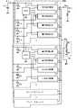
- FIG. 1 is a schematic block diagram showing an example (four units) of the power supply system device according to the first embodiment.
- FIG. 2 is a circuit block diagram showing an example (four units) of the power supply system device according to the first embodiment.
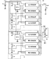
- FIG. 3 is a circuit block diagram showing an example (two units) of the power supply system device according to the first embodiment.
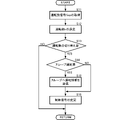
- FIG. 4 is a flowchart illustrating an example of processing executed by the MPU on the master side.
- FIG. 5 is a flowchart illustrating an example of processing executed by the MPU on the slave side.
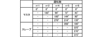
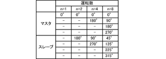
- FIG. 6 is a table showing an example of the first mode of phase control.
- FIG. 7 is a graph showing the relationship between the output current and the output voltage for explaining the concept of switching the number of operations.
- FIG. 1 is a schematic block diagram showing an example (four units) of the power supply system device according to the first embodiment.
- FIG. 2 is a circuit block diagram showing an example (four units) of the power supply system device according to the first embodiment.
- FIG. 8 is a table showing an example of the second mode of phase control.
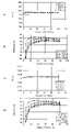
- 9A, 9B, 9C, and 9D are graphs of output voltage and power conversion efficiency versus output current using embodiments of the present invention.
- FIG. 10 is an equivalent circuit diagram of the power conversion circuit according to the first embodiment.
- FIG. 11 is an equivalent circuit diagram showing an example of the feedback signal generator according to this embodiment.
- FIG. 12 is an equivalent circuit diagram of the feedback signal generator of the power supply system device according to the second embodiment.
- FIG. 1 is a schematic block diagram showing an example (four units) of the power supply system device according to the first embodiment.
- FIG. 2 is a circuit block diagram showing an example (four units) of the power supply system device according to the first embodiment.
- the power supply system device 10 includes converter units 11 and 12, and a voltage dividing circuit 60.
- FIG. Converter unit 11 and converter unit 12 are connected in parallel to common input terminal Pin and common output terminal Pout.
- the power supply system unit 10U4 includes four converter units 11-14 and a voltage dividing circuit 60.
- the four converter units 11-14 are connected in parallel to a common input terminal Pin and a common output terminal Pout.
- the common input terminal Pin is connected to an external DC voltage source (input power supply).
- the power supply system unit 10 is supplied with a DC common input voltage Vin from a common input terminal Pin.
- a common output terminal Pout is connected to a load Ro. The voltage of the common output terminal Pout becomes the common output voltage Vout of the power supply system device 10 .
- the four converter units 11-14 have the same circuit configuration except for the control mode of each MPU.
- the MPUs of the four converter units 11-14 are capable of mutual data communication, one MPU performs master control, and the other MPU performs slave control.
- the MPU 21 of the converter unit 11 performs master control
- the MPUs of the other converter units 12-14 perform slave control.
- the MPU of each of these converter units 11-14 corresponds to the "common control section" of the present invention.
- the converter unit 11 includes an MPU 21, a power conversion circuit 311, a power conversion circuit 312, a power conversion circuit 313, and a power conversion circuit 314.
- the converter unit 11 also includes an input capacitor Ci11, an input capacitor Ci12, an input capacitor Ci13, and an input capacitor Ci14.
- the converter unit 12 includes an MPU 22, a power conversion circuit 321, a power conversion circuit 322, a power conversion circuit 323, and a power conversion circuit 324.
- the converter unit 12 also includes an input capacitor Ci21, an input capacitor Ci22, an input capacitor Ci23, and an input capacitor Ci24.
- the converter units 13 and 14 each include an MPU and a plurality of power conversion circuits. Further, the converter units 13 and 14 each have an input capacitor for each power conversion circuit.
- the voltage dividing circuit 60 is a series circuit of resistors R61 and R62. One end of the series circuit of the resistors R61 and R62 is connected to each power conversion circuit of the four converter units 11-14. One end of a series circuit of resistors R61 and R62 is connected to a reference potential. A connection point between the resistor R61 and the resistor R62 is connected to the MPU of each of the four converter units 11-14.
- the MPU of the converter unit serving as the master for example, the MPU 21 of the converter unit 11 generates operating information including the operating number based on the operating number signal Sop.
- the operation information includes the number of operations on the master side, the presence or absence of operation on the slave side, the number of operations on the slave side, the phase of the control signal, and the like.
- the MPU 21 generates control signals for the power conversion circuits 311, 312, 313, and 314 of the converter unit 11 based on the operating information, and outputs the control signals to the power conversion circuits 311, 312, 313, and 314.
- the MPU 21 transmits operation information to each MPU of the converter units 12-14 that serve as slaves. That is, the master MPU 21 determines whether operation is necessary on the slave side, generates operation information according to the content of the determination, and transmits the operation information to each MPU serving as a slave.
- Each MPU serving as a slave generates and outputs a control signal for a plurality of power conversion circuits of the converter units 12-14 that it controls, based on the operation information.
- the converter units 12-14 serving as slaves perform power conversion based on control signals from the respective MPUs.
- the MPU 21 when operating only the converter unit 11, the MPU 21 operates only the converter unit 11.
- the MPU of each converter unit when operating two converter units 11 and 12, the MPU of each converter unit synchronizes and operates the two converter units 11 and 12 in parallel.
- the MPU of each converter unit when operating the three converter units 11-13, the MPU of each converter unit synchronizes and operates the three converter units 11-13 in parallel.
- the MPU of each converter unit when operating the four converter units 11-14, the MPU of each converter unit synchronizes and operates the four converter units 11-14 in parallel.
- the power supply system unit 10U4 can easily respond to changes in the number of power conversion circuits to be operated according to the state of the load. Therefore, the power supply system unit 10U4 can supply an appropriate common output voltage Vout according to the state of the load to the load.
- the MPU 21 when operating only the converter unit 11, the MPU 21 operates the converter unit 11 as a multiphase converter.
- each MPU synchronizes and operates the two converter units 11 and 12 as a multi-phase converter.
- each MPU when operating the three converter units 11-13, each MPU synchronizes and operates the three converter units 11-13 as a multi-phase converter.
- each MPU When operating the converter units 11-14, each MPU synchronizes and operates the four converter units 11-14 as a multi-phase converter. That is, the MPU of each converter unit controls the phase of the oscillation signal of the control signal output to the power conversion circuit to be operated according to the number of operations.
- the converter units to be operated are synchronized and multi-phase controlled.
- the power supply system unit 10U4 can reduce the ripple voltage of the common output voltage Vout.
- the number of control signals generated and output by one MPU can be reduced. Therefore, the configuration processing of the MPU can be simplified. And even if such a simplified MPU is used, various control modes as described above can be easily and reliably realized. At this time, since the MPU is a programmable digital electronic circuit, the above control can be realized more easily than using an analog circuit. Note that the number of converter units constituting the power supply system device is not limited to four, and as long as there are a plurality of units (two or more), the configuration of the present invention can be applied and the same effects can be obtained. .
- FIG. 3 is a circuit block diagram showing an example (2 units) of the power supply system device according to the first embodiment.
- power supply system device 10 includes converter units 11 and 12 , and voltage dividing circuit 60 .
- Converter unit 11 and converter unit 12 are connected in parallel to common input terminal Pin and common output terminal Pout.
- the common input terminal Pin is connected to an external DC voltage source (input power supply).
- the power supply system unit 10 is supplied with a DC common input voltage Vin from a common input terminal Pin.
- a common output terminal Pout is connected to a load Ro. The voltage of the common output terminal Pout becomes the common output voltage Vout of the power supply system device 10 .
- the converter unit 11 and the converter unit 12 have the same circuit configuration except for the control modes of the MPU21 and MPU22.
- the MPU 21 of the converter unit 11 and the MPU 22 of the converter unit 12 are capable of mutual data communication, one performing master control and the other performing slave control.
- the MPU 21 of the converter unit 11 performs master control
- the MPU 22 of the converter unit 12 performs slave control.
- the converter unit 11 includes an MPU 21, a power conversion circuit 311, a power conversion circuit 312, a power conversion circuit 313, and a power conversion circuit 314.
- the converter unit 11 also includes an input capacitor Ci11, an input capacitor Ci12, an input capacitor Ci13, and an input capacitor Ci14.
- the converter unit 12 includes an MPU 22, a power conversion circuit 321, a power conversion circuit 322, a power conversion circuit 323, and a power conversion circuit 324.
- the converter unit 12 also includes an input capacitor Ci21, an input capacitor Ci22, an input capacitor Ci23, and an input capacitor Ci24.
- the voltage dividing circuit 60 is a series circuit of resistors R61 and R62.
- One end of the series circuit of resistor R61 and resistor R62 is connected to power conversion circuit 311, power conversion circuit 312, power conversion circuit 313, and power conversion circuit 314 of converter unit 11, power conversion circuit 321 of converter unit 12, It is connected to power conversion circuit 322 , power conversion circuit 323 , and power conversion circuit 324 .
- One end of a series circuit of resistors R61 and R62 is connected to a reference potential.
- a connection point between the resistor R61 and the resistor R62 is connected to MPU21 and MPU22.
- the MPU 21 is connected to the common input terminal Pin and supplied with power through the common input terminal Pin.
- This power supply line is connected to the ground reference potential through an input capacitor Ci11.
- the MPU 21 is a programmable Micro Processing Unit made up of digital electronic circuits.
- the MPU 21 is a device capable of executing programmable arithmetic processing.
- the MPU 21 generates control signals (oscillation control signals) to drive units of the plurality of power conversion circuits 311, 312, 313, and 314 by programmable arithmetic processing.
- the MPU 21 is connected to a plurality of power conversion circuits 311, 312, 313, and 314. MPU21 outputs a control signal with respect to each of several power inverter circuits 311,312,313,314.
- the MPU 21 outputs a control signal according to the power conversion circuit to the power conversion circuit to be operated (the power conversion circuit that enables operation) among the plurality of power conversion circuits 311, 312, 313, and 314, No control signal is output to the power conversion circuit that is not in operation (the power conversion circuit that disables its operation).
- the MPU 21 determines the number of power conversion circuits to be operated using the voltage obtained by dividing the operating number signal Sop based on the common output voltage Vout by the voltage dividing circuit 60 .
- the control signal output from the MPU 21 to each power conversion circuit contains an oscillation signal composed of the switching frequency of each power conversion circuit.
- the oscillation signal of each control signal has a phase difference, and the MPU 21 sets this phase difference.
- the power conversion circuit 311, the power conversion circuit 312, the power conversion circuit 313, and the power conversion circuit 314 are composed of analog electronic circuits. Note that specific circuit configurations of the power conversion circuit 311, the power conversion circuit 312, the power conversion circuit 313, and the power conversion circuit 314 will be described later.
- the power conversion circuit 311, the power conversion circuit 312, the power conversion circuit 313, and the power conversion circuit 314 are connected to a common input terminal Pin and supplied with power through the common input terminal Pin.
- the power supply line of the power conversion circuit 311 is connected to the ground reference potential through the input capacitor Ci11.
- the power supply line of the power conversion circuit 312 is connected to the ground reference potential through the input capacitor Ci12.
- the power supply line of the power conversion circuit 313 is connected to the ground reference potential through the input capacitor Ci13.
- the power supply line of the power conversion circuit 314 is connected to the ground reference potential through the input capacitor Ci14.
- the output terminals of the power conversion circuit 311, the power conversion circuit 312, the power conversion circuit 313, and the power conversion circuit 314 are connected to a common output terminal Pout.
- the power conversion circuit 311, the power conversion circuit 312, the power conversion circuit 313, and the power conversion circuit 314 each have a voltage feedback signal generator and an individual voltage feedback loop.
- the power conversion circuit 311, the power conversion circuit 312, the power conversion circuit 313, and the power conversion circuit 314 receive control signals from the MPU 21, perform switching control using PWM control, and perform power conversion. I do.
- the power conversion circuit 311, the power conversion circuit 312, the power conversion circuit 313, and the power conversion circuit 314 respond to the common output voltage Vout based on feedback signals using respective individual voltage feedback loops, that is, , to appropriately and quickly control the inductor current according to the load state.
- the control signals supplied to the power conversion circuit 311, the power conversion circuit 312, the power conversion circuit 313, and the power conversion circuit 314 have a phase difference, the power conversion circuit 311, the power conversion circuit 312, and the power conversion circuit 313 , and the power conversion circuit 314 are multi-phase controlled. Therefore, the ripple voltage of the common output voltage Vout is suppressed.
- the MPU 22 is connected to the common input terminal Pin and supplied with power through the common input terminal Pin.
- This power supply line is connected to the ground reference potential through an input capacitor Ci21.
- the MPU 22 is a programmable Micro Processing Unit made up of digital electronic circuits.
- the MPU 22 is a device capable of executing programmable arithmetic processing.
- the MPU 22 generates control signals (oscillation control signals) to drive units of the plurality of power conversion circuits 321, 322, 323, and 324 by programmable arithmetic processing.
- the MPU 22 is connected to a plurality of power conversion circuits 321, 322, 323, and 324. MPU22 outputs a control signal with respect to each of several power inverter circuits 321,322,323,324.
- the MPU 22 generates and outputs control signals for the plurality of power conversion circuits 321, 322, 323, and 324 based on the operation information (details will be described later) from the MPU 21.
- a control signal output from the MPU 22 to each power conversion circuit includes an oscillation signal having a switching frequency of each power conversion circuit.
- the oscillation signal of each control signal has a phase difference, and the MPU 22 sets this phase difference.
- the power conversion circuit 321, the power conversion circuit 322, the power conversion circuit 323, and the power conversion circuit 324 are composed of analog electronic circuits.
- the specific circuit configurations of the power conversion circuits 321 , 322 , 323 and 324 are the same as those of the power conversion circuits 311 , 312 , 313 and 314 .
- the power conversion circuit 321, the power conversion circuit 322, the power conversion circuit 323, and the power conversion circuit 324 are connected to a common input terminal Pin and supplied with power through the common input terminal Pin.
- the power supply line of the power conversion circuit 321 is connected to the ground reference potential through the input capacitor Ci21.
- the power supply line of the power conversion circuit 322 is connected to the ground reference potential through the input capacitor Ci22.
- the power supply line of the power conversion circuit 323 is connected to the ground reference potential through the input capacitor Ci23.
- the power supply line of the power conversion circuit 324 is connected to the ground reference potential through the input capacitor Ci24.
- the output terminals of the power conversion circuit 321, the power conversion circuit 322, the power conversion circuit 323, and the power conversion circuit 324 are connected to a common output terminal Pout.
- the power conversion circuit 321, the power conversion circuit 322, the power conversion circuit 323, and the power conversion circuit 324 each include a voltage feedback signal generation section and an individual voltage feedback loop.
- the power conversion circuit 321, the power conversion circuit 322, the power conversion circuit 323, and the power conversion circuit 324 receive a control signal from the MPU 22, perform switching control using PWM control, and perform power conversion to each. I do.
- the power conversion circuit 321, the power conversion circuit 322, the power conversion circuit 323, and the power conversion circuit 324 respond to the common output voltage Vout based on feedback signals using respective individual voltage feedback loops, that is, , to appropriately and quickly control the inductor current according to the load state.
- the control signals supplied to the power conversion circuit 321, the power conversion circuit 322, the power conversion circuit 323, and the power conversion circuit 324 have a phase difference, the power conversion circuit 321, the power conversion circuit 322, and the power conversion circuit 323 , and the power conversion circuit 324 are multi-phase controlled. Therefore, the ripple voltage of the common output voltage Vout is suppressed.
- the MPU 21 of the converter unit 11 on the master side generates operating information including the operating number based on the operating number signal Sop.
- the operation information includes the number of operations on the master side, the presence or absence of operation on the slave side, the number of operations on the slave side, the phase of the control signal, and the like.
- the MPU 21 generates control signals for the power conversion circuits 311, 312, 313, and 314 of the converter unit 11 based on the operating information, and outputs the control signals to the power conversion circuits 311, 312, 313, and 314.
- the MPU 21 transmits operating information to the MPU 22 of the converter unit 12 on the slave side. That is, the MPU 21, which is the master, determines whether operation is necessary on the slave side, generates operation information according to the content of the determination, and transmits it to the MPU 22 on the slave side.
- FIG. 4 is a flowchart illustrating an example of processing executed by the MPU on the master side.
- the MPU 21 acquires the operation number signal Sop (S11). The MPU 21 determines the operation number n from the level of the operation number signal Sop (S12). The MPU 21 determines whether or not it is necessary to switch the number of operations (S13).
- the MPU 21 determines whether the operation on the slave side is necessary (S14). On the other hand, the MPU 21 maintains the current control state if it is not necessary to switch the number of operations (S13: NO).
- the MPU 21 transmits operation information to the slave MPU 22 (S15), and changes the control signal within the converter unit 11 (S16).
- the converter unit 11 performs power conversion based on the control signal from the MPU 21.
- the MPU 22 generates control signals for the power conversion circuits 321, 322, 323, and 324 of the converter unit 12 based on the operating information, and outputs the control signals to the power conversion circuits 321, 322, 323, and 324.
- FIG. 5 is a flowchart illustrating an example of processing executed by the MPU on the slave side.
- the MPU 22 receives operation information from the MPU 21 on the master side (S51).
- the MPU 22 needs to operate in the converter unit 12 on the slave side, and if each power conversion circuit of the converter unit 12 is not in operation (S52: NO), the MPU 22 generates a control signal for the power conversion circuit to be operated, Output is started (S53).
- the MPU 22 changes the control signal in the converter unit 12 (S55). .
- the MPU 22 selects the plurality of power conversion circuits 321, 322, 323 of the converter unit 12, 324 stops outputting the control signal (S56).
- the converter unit 12 performs power conversion based on the control signal from the MPU 22.
- the MPU 21 when operating only the converter unit 11, the MPU 21 operates only the converter unit 11.
- MPU 21 and MPU 22 are synchronized and converter unit 11 and converter unit 12 are operated in parallel.
- the power supply system unit 10 can easily cope with changes in the number of power conversion circuits to be operated according to the state of the load. Therefore, the power supply system unit 10 can supply the load with an appropriate common output voltage Vout according to the state of the load.
- the MPU 21 when operating only the converter unit 11, the MPU 21 operates the converter unit 11 as a multiphase converter.
- the MPU 21 and the MPU 22 are synchronized so that the converter unit 11 and the converter unit 12 are integrally operated as a multiphase converter. That is, MPU21 and MPU22 control the phase of the oscillation signal of the control signal output to the power inverter circuit of operation object according to the number of operations.
- FIG. 6 is a table showing an example of the first mode of phase control.
- FIG. 7 is a graph showing the relationship between the output current and the output voltage for explaining the concept of switching the number of operations. Note that FIG. 7 is a graph including cases where the number of operations is more than eight. If the number of operations is required to be more than 8, it can be handled by increasing the number of slave converter units described above.
- the range of the output current Iout that can be handled by the master-side converter unit is the range that cannot be handled by the master-side converter unit alone.
- a master-side converter unit and a slave-side converter unit are used.
- the MPU 21 on the master side outputs a control signal to one power conversion circuit of the converter unit 11 to operate this power conversion circuit.
- the MPU 21 on the master side determines to operate the converter unit 12 together with the converter unit 11, and transmits this operation information to the MPU 22 on the slave side.
- the MPU 22 on the slave side receives this operation information.
- the MPU 21 on the master side outputs control signals to the four power conversion circuits of the converter unit 11 to operate these power conversion circuits.
- the MPU 22 on the slave side outputs a control signal to one power conversion circuit of the converter unit 12 to operate this power conversion circuit.
- the MPU 21 on the master side determines to operate the converter unit 12 together with the converter unit 11, and transmits this operation information to the MPU 22 on the slave side.
- the MPU 22 on the slave side receives this operation information.
- the MPU 21 on the master side outputs control signals to the four power conversion circuits of the converter unit 11 to operate these power conversion circuits.
- the MPU 22 on the slave side outputs control signals to the four power conversion circuits of the converter unit 12 to operate the power conversion circuits.
- the master-side converter unit is operated within the range of the output current Iout that can be handled only by the master-side converter unit. Therefore, unnecessary operation of the slave-side converter unit can be suppressed, and unnecessary power loss in the slave-side converter unit can be suppressed.
- the number of control signals generated and output by one MPU can be reduced. Therefore, the configuration processing of the MPU can be simplified. And even if such a simplified MPU is used, various control modes as described above can be easily and reliably realized. At this time, since the MPU is a programmable digital electronic circuit, the above control can be realized more easily than using an analog circuit.
- FIG. 8 is a table showing an example of the second mode of phase control.
- the MPU 21 on the master side outputs a control signal to one power conversion circuit of the converter unit 11 to operate this power conversion circuit.
- the MPU 21 determines to operate the converter unit 12 together with the converter unit 11, and transmits this operation information to the MPU 22 on the slave side.
- the MPU 22 on the slave side receives this operation information.
- the MPU 22 on the master side outputs a control signal to one power conversion circuit of the converter unit 12 to operate this power conversion circuit.
- the MPU 22 on the master side outputs control signals to the two power conversion circuits of the converter unit 12 to operate these power conversion circuits.
- the MPU 21 on the master side outputs control signals to the four power conversion circuits of the converter unit 11 to operate these power conversion circuits.
- the MPU 22 on the slave side outputs control signals to the four power conversion circuits of the converter unit 12 to operate the power conversion circuits.
- the master-side converter unit and the slave-side converter unit are operated in synchronization. Therefore, the power loss can be averaged and distributed between the master-side converter unit and the slave-side converter unit.
- phase difference between a plurality of control signals output by one MPU can be increased. This makes it possible to more reliably output a plurality of control signals having desired phase differences. Therefore, the ripple voltage can be reduced more reliably and accurately.
- this control can temporally disperse noise and heat generation.
- the number of control signals generated and output by one MPU can be reduced. Therefore, the configuration processing of the MPU can be simplified. And even if such a simplified MPU is used, various control modes as described above can be easily and reliably realized. At this time, since the MPU is a programmable digital electronic circuit, the above control can be realized more easily than using an analog circuit.
- the master-side converter unit and the slave-side converter unit have the same configuration. Therefore, parts can be shared between the master-side converter unit and the slave-side converter unit, and a power supply system device excellent in practical use can be constructed in which cost reduction, design period reduction, etc. can be realized.
- phase control of the first mode and the second mode described above is merely an example, and the master-side converter unit and the slave-side converter unit are synchronized and the phases of at least some of the control signals are made different. If necessary, other phase control may be performed. Furthermore, by making all the control signals out of phase, the power supply system unit 10 can be pseudo-high-frequency operated, and the power loss can be further averaged and dispersed.
- the characteristics as shown in FIG. Then, depending on the number of operations n, the mode of use of the master-side converter unit and the slave-side converter unit, that is, whether only the converter unit is sufficient or whether the master-side converter unit and the slave-side converter unit are required set. Then, the phase control is set according to the set usage mode. Even in such a case, stable and highly accurate output characteristics and high power conversion efficiency can be achieved.
- 9(A), 9(B), 9(C), and 9(D) are graphs showing output voltage and power conversion efficiency with respect to output current when using the embodiment of the present invention.
- 9A shows output voltage characteristics in a configuration corresponding to an output current of 100A
- FIG. 9B shows power conversion efficiency in a configuration corresponding to an output current of 100A
- FIG. 9(C) shows output voltage characteristics in a configuration corresponding to an output current of 50A
- FIG. 9(D) shows power conversion efficiency in a configuration corresponding to an output current of 50A.
- the power conversion circuit has, for example, the following configuration. Since the power conversion circuits 311, 312, 313, 314, 321, 322, 323, and 324 have the same circuit configuration, the power conversion circuit 311 will be described below as an example.
- FIG. 10 is an equivalent circuit diagram of the power conversion circuit according to the first embodiment.
- the power conversion circuit 311 includes a drive section 41, a switching element Q11, a switching element Q12, an inductor L1, an output capacitor Co1, a resistor RL1, a capacitor CL1, and a feedback signal generation section 51.
- the feedback signal generator 51 has terminals 511 , 512 , 513 , and 514 . Terminals 511, 512, 513, and 514 may have physical terminal structures, but are functionally connections to other circuit elements and the like.
- a circuit composed of the switching element Q11 and the switching element Q12 corresponds to the "switching circuit" of the present invention.
- the drive unit 41 is connected to the common input terminal Pin and is supplied with power through the common input terminal Pin.
- the driving section 41 is formed by an analog circuit. Further, the driving section 41 and the feedback signal generating section 51 form an individual analog control section.
- the individual analog control unit and the switching circuit are formed, for example, by an integrally integrated FET built-in PWM control IC.
- the drive unit 41 receives the above-described phase-controlled control signal from the MPU 21 .
- a feedback signal obtained by synthesizing the voltage feedback signal and the current feedback signal is input from the feedback signal generating section 51 to the driving section 41 . That is, the individual voltage feedback signal is fed back to the drive unit 41 via the individual voltage feedback control loop vFB as indicated by the two-dot chain line in FIG. 8, and via the individual current feedback control loop iFB as indicated by the dotted line in FIG.
- An individual current feedback signal is fed back to the driver 41 .
- the individual voltage feedback control loop vFB and the individual current feedback control loop iFB will be described in the feedback signal generator 51, which will be described later.
- the drive unit 41 generates a switching control signal using PWM (pulse width modulation) control for the switching element Q11 and the switching element Q12 from the control signal and the feedback signal. Since the driving section 41 is composed of an analog electronic circuit, it can output a PWM control signal corresponding to the voltage of the feedback signal at high speed.
- PWM pulse width modulation
- the gate of the switching element Q12 is connected to the driving section 41, the drain is connected to the common input terminal Pin, and the source is connected to the drain of the switching element Q11.
- the switching element Q11 has a gate connected to the driving section 41 and a source connected to the ground reference potential.
- a PWM control signal for the switching element Q12 is input from the driving section 41 to the gate of the switching element Q12.
- a switching control signal for the switching element Q11 is input from the driving section 41 to the gate of the switching element Q11.
- One end of the inductor L1 is connected to a connection point between the source of the switching element Q12 and the drain of the switching element Q11.
- the other end of the inductor L1 is connected to the common output terminal Pout.
- the other end of inductor L1 is connected to the ground reference potential through output capacitor Co1.
- a series circuit of the resistor RL1 and the capacitor CL1 is connected in parallel to the inductor L1.
- This circuit corresponds to the "inductor current detection circuit” of the present invention.
- the resistor RL1 corresponds to the “detection resistor” of the invention, and the capacitor CL1 corresponds to the “detection capacitor” of the invention.
- a connection point between the resistor RL1 and the capacitor CL1 is connected to the terminal 512 of the feedback signal generator 51 . That is, the inductor current detection circuit for the inductor L1 can output the voltage across the capacitor CL1 to the feedback signal generator 51 as a detection signal for the inductor current iL1 of the inductor L1.
- the inductor current detection circuit sets the inductance of the inductor L1, the resistance value of the equivalent series resistance Rs1 of the inductor L1, the resistance value of the resistor RL1, and the capacitance of the capacitor CL1 to a specific relationship, so that the current flowing through the inductor L1 Inductor current iL1 can be sensed losslessly.
- FIG. 11 is an equivalent circuit diagram showing an example of the feedback signal generator according to this embodiment.
- the feedback signal generator 51 includes terminals 511, 512, 513, and 514. Terminals 511, 512, 513, and 514 are provided.
- the terminal 511 is connected to the common output terminal Pout, in other words, the parallel connection of the output terminals of the power conversion circuits 311 , 312 , 313 , and 314 .
- a terminal 512 is connected to a connection point between the resistor RL1 and the capacitor CL1.
- Terminal 513 is connected to drive unit 41 .
- the terminal 514 is connected in parallel with the same terminal as the terminal 514 in the feedback signal generation units of the other power conversion circuits 312 , 313 and 314 . That is, the terminal 514 of the feedback signal generator 51 of the power converter circuit 311 and the same terminal as the terminal 514 of the feedback signal generators of the other power converter circuits 312, 313, and 314 are connected to a common node.
- the common node is the output portion of the operation number signal Sop and is connected to the MPU 20 through the voltage dividing circuit 60 .
- the feedback signal generation unit 51 is configured by an analog circuit, and based on the common output voltage Vout, the inductor current iL1 of the inductor L1, and the common node voltage (common bus signal (operating number signal) voltage), the driving unit 41 generates a feedback signal to
- the feedback signal generation section 51 includes an individual current signal generation section 551, a common signal generation section 552, an individual feedback signal generation section 553, and a voltage adjustment circuit 554.
- the individual current signal generator 551 includes an amplifier U51, a resistor R51, a resistor R52, a resistor R53, and a resistor R54.
- the inverting input terminal of amplifier U51 is connected to terminal 511 through resistor R51.
- the non-inverting input terminal of amplifier U51 is connected to terminal 512 through resistor R52.
- the resistance value of the resistor R51 and the resistance value of the resistor R52 are the same.
- a resistor R53 is connected between the non-inverting input terminal and the ground reference potential.
- the output terminal of amplifier U51 is connected to the inverting input terminal of amplifier U51 through resistor R54.
- the resistance value of resistor R53 and the resistance value of resistor R54 are the same.
- a driving power supply VDD is supplied to the amplifier U51. With this circuit configuration, the individual current signal generator 551 implements a differential amplifier circuit.
- the terminal 511 is connected to the common output terminal Pout, and the terminal 512 is connected to the connection point between the capacitor CL1 and the resistor RL1.
- a potential difference corresponding to the inductor current iL1 is generated between the non-inverting input terminal and the inverting input terminal of the amplifier U51.
- a signal based on the inductor current iL1 is amplified by a predetermined amplification factor and output as an individual current signal.
- the common signal generator 552 includes an amplifier U52 and a diode D52.
- the non-inverting input terminal of amplifier U52 is connected to the output terminal of amplifier U51.
- the output terminal of amplifier U52 is connected through diode D52 to the inverting input terminal of amplifier U52.
- the anode of the diode D52 is connected to the output terminal, and the cathode of the diode D52 is connected to the inverting input terminal.
- the inverting input terminal is connected to terminal 514, the common node.
- a driving power supply VDD is supplied to the amplifier U52.
- the common signal generator 552 implements a circuit for holding the maximum value of individual current signals for the plurality of power conversion circuits 311 , 312 , 313 , and 314 .
- a signal consisting of the maximum value of the individual current signals is the operation number signal Sop, and corresponds to the "common bus signal" of the present invention.
- the individual feedback signal generator 553 includes an amplifier U53, an amplifier U54, a transistor Tr55, a resistor R55, a resistor R56, a resistor R57, a resistor R58, a resistor R551, and a resistor R552.
- the inverting input terminal of amplifier U53 is connected to the output terminal of amplifier U51 through resistor R55.
- the non-inverting input terminal of amplifier U53 is connected to the cathode of diode D52 and to terminal 514 through resistor R56.
- the resistance value of resistor R55 and the resistance value of resistor R56 are the same.
- Resistor R57 is connected between the non-inverting input terminal of amplifier U53 and the ground reference potential.
- the output terminal of amplifier U53 is connected to the inverting input terminal of amplifier U53 through resistor R58.
- the resistance value of resistor R57 and the resistance value of resistor R58 are the same.
- a driving power supply VDD is supplied to the amplifier U53.
- the non-inverting input terminal of amplifier U54 is connected to the output terminal of amplifier U53.
- the output terminal of the amplifier U54 is connected to the base of an NPN transistor Tr55.
- the collector of transistor Tr55 is connected to terminal 511 through resistor R551.
- the emitter of transistor Tr55 is connected to the ground reference potential through resistor R552.
- the emitter of transistor Tr55 is connected to the inverting input terminal of amplifier U54.
- An individual current signal is input to the inverting input terminal of the amplifier U53, and a common bus signal is input to the non-inverting input terminal.
- a potential difference between the common bus signal and the individual current signal is generated between the non-inverting input terminal and the inverting input terminal of the amplifier U51.
- a signal based on the potential difference between the common bus signal and the individual current signal is amplified by a predetermined amplification factor and output to the amplifier U54.
- a voltage-current conversion circuit is realized by a circuit consisting of an amplifier U54, a transistor Tr55, and a resistor R552. Specifically, in this circuit, when a differential signal (differential voltage) is applied to the non-inverting input terminal of the amplifier U54, a differential signal (differential current Iadj) flows between the collector and emitter of the transistor Tr55. This differential current corresponds to the individual current feedback signal.
- the voltage at the connection point between the resistors R551 and R11 (the collector of the transistor Tr55) becomes Vout-(Rr551 ⁇ Iadj).
- Rr551 is the resistance value of the resistor R551.
- the common output voltage Vout is the same as the individual voltage feedback signal. Therefore, the individual feedback signal generator 553 can generate and output a feedback signal obtained by synthesizing the individual current feedback signal and the individual voltage feedback signal.
- the voltage adjustment circuit 554 is a so-called voltage dividing circuit and includes a series circuit of resistors R11 and R12.
- the resistor R11 is connected to a connection point between the collector of the transistor Tr55 of the individual feedback signal generator 553 and the resistor R551.
- Resistor R12 is connected to the ground reference potential.
- a connection point between the resistor R11 and the resistor R12 is connected to the terminal 513 .
- a terminal 513 is an output terminal for the feedback signal in the feedback signal generator 51 .
- the voltage adjusting circuit 554 converts the voltage of the feedback signal output from the individual feedback signal generating section 553 into a voltage that can be handled by the driving section 41 and outputs it to the terminal 513 .
- the feedback signal output to the terminal 513 is fed back to the driving section 41 .
- an individual voltage feedback control loop vFB (a chain double-dashed line in FIG. 10) and an individual current feedback control loop iFB (a dotted line in FIG. 10) as described in the drive section 41 above are implemented.
- the drive unit 41 uses this feedback signal to perform the PWM control as described above.
- the common output voltage Vout responds at high speed according to the load fluctuation. That is, when the common output voltage Vout fluctuates according to load fluctuations, this is reflected in the individual voltage feedback signals included in the feedback signal.
- the driving section 41 uses the change in the individual voltage feedback signal to perform PWM control so as to stabilize the common output voltage Vout.
- the power conversion circuit 311 and the plurality of power conversion circuits 312, 313, and 314 connected in parallel respond quickly to a sudden change in the common output voltage Vout and stabilize the common output voltage Vout.
- each individual analog control unit is composed of an analog electronic circuit, it is possible to realize faster response and stabilization of the common output voltage Vout.
- control of this individual voltage feedback signal is substantially effected by the control by the power conversion circuit that makes a large contribution to the common output voltage Vout at that time.
- the power conversion circuit 311 substantially performs PWM control to stabilize the common output voltage Vout.
- the power conversion circuit 312 substantially performs PWM control to stabilize the common output voltage Vout.
- the inductor currents of multiple power conversion circuits connected in parallel can be averaged.
- the power loss of a plurality of power conversion circuits can be averaged.
- the power supply system device 10 can further improve power efficiency, disperse heat generated by power loss, and improve reliability while realizing the effects of multiphase control using master-slave control.
- the individual analog control unit is composed of an analog electronic circuit, the power supply system unit 10 can realize the control of averaging the power loss at high speed.
- FIG. 12 is an equivalent circuit diagram of the feedback signal generator of the power supply system device according to the second embodiment.
- the feedback signal generation unit 51R of the power supply system device has a common signal generation unit 53R is used.
- the rest of the configuration of the feedback signal generation section 51R is the same as that of the feedback signal generation section 51, and the description of the similar portions will be omitted.
- the common signal generator 53R includes a resistor R60. Resistor R60 is connected between the output terminal and the inverting input terminal of amplifier U52. This configuration implements an average value calculation circuit comprising amplifier U52 and resistor R60.
- the common signal generator 53R uses this average value signal as a common bus signal. Thus, even if the average value signal is used as the common bus signal, it is possible to realize processing similar to that for the maximum value signal described above.
- the method of selecting the power inverter circuit to be operated may be based on the layout pattern of the plurality of power inverter circuits on the circuit board. For example, power inverter circuits with long distances are selected in order. As a result, the heat generated on the circuit board can be dispersed, and the reliability of the power supply system device can be improved.
- the number of power conversion circuits provided in one converter unit is four.
- the number of power conversion circuits provided in one converter unit may be plural.
Landscapes
- Engineering & Computer Science (AREA)
- Power Engineering (AREA)
- Dc-Dc Converters (AREA)
- Supply And Distribution Of Alternating Current (AREA)
- Inverter Devices (AREA)
Abstract
電源システム装置(10)のコンバータユニット(11、12)は、それぞれに、個別電圧帰還ループを用いたフィードバック制御を行う。コンバータユニット(11)をマスタ制御とし、コンバータユニット(12)をスレーブ制御とするように、発振制御信号を同期するマスタスレーブ制御を実行する。発振制御信号は、動作対象の電力変換回路の個数に応じて、複数の電力変換回路間で位相差が生じるように設定される。電源システム装置(10)は、入力電源の電圧をコンバータユニット(11、12)の複数の電力変換回路を用いて電圧変換する電圧変換動作を、コンバータユニット(11、12)で同期させて実行しながら、負荷に電力を供給する。
Description
本発明は、複数の電力変換回路を備えた電源システム装置に関する。
特許文献1には、システムスイッチング電源装置が記載されている。特許文献1のシステムスイッチング電源装置は、インダクタ、スイッチング回路、および、個別アナログ制御部をそれぞれに備える複数の電力変換回路と、複数の電力変換回路に対して発振制御信号を出力する共通制御部とを備える。
個別アナログ制御部は、アナログ電子回路によって形成されている。個別アナログ制御部は、電力変換回路の出力状態を検出して帰還信号を生成する帰還信号生成部と、帰還信号に応じてスイッチング回路の駆動制御を行う駆動部を備える。共通制御部は、プログラマブルな演算処理を実行できるデジタル電子回路によって形成されている。
しかしながら、特許文献1に示す構成では、電力変換回路の必要な個数がさらに多くなると、共通制御部の制御がより複雑になり、難しくなる。共通制御部においては、数多くの信号入力端子と信号出力端子を備えることが必要となり、共通制御部が大型化する。また、電力変換回路の必要な個数に応じた設計変更や設計調整を行わなければならず、システムの変更が容易ではなかった。
したがって、本発明の目的は、必要な電力変換回路の個数変更に容易に対応可能な電源システム装置を提供することにある。
この発明の電源システム装置は、共通制御部および個別アナログ制御部を有するユニット制御部をそれぞれに備える複数のコンバータユニットを備える。
複数のコンバータユニットのそれぞれは、インダクタとスイッチング回路と個別アナログ制御部とをそれぞれに備える複数の電力変換回路と、複数の電力変換回路の入力部が並列に接続され、入力電源に接続される共通入力端子と、複数の電力変換回路の出力部が並列接続され、負荷に接続される共通出力端子と、複数の電力変換回路に対して、発振制御信号を出力する前記共通制御部と、を備える。個別アナログ制御部は、共通出力端子の出力電圧を検出して電圧帰還信号を生成し、電圧帰還信号をフィードバックする電圧帰還信号生成部および個別電圧帰還ループと、電圧帰還信号を用いてスイッチング回路のスイッチング素子を駆動する駆動部と、を備える。
ユニット制御部は、個別電圧帰還ループを用いたフィードバック制御を行いながら、複数のコンバータユニットにおいて、一方のコンバータユニットをマスタ制御とし、他方のコンバータユニットをスレーブ制御とするように、発振制御信号を同期するマスタスレーブ制御を実行する。ユニット制御部は、入力電源の電圧を複数のコンバータユニットの複数の電力変換回路を用いて電圧変換する電圧変換動作を、複数のコンバータユニットで同期させて実行しながら、負荷に電力を供給する。
この構成では、負荷の電力に応じて必要な電力変換回路の個数が変化しても、マスタスレーブ制御によって、電力変換回路の運転数、位相が自動的に適切に制御される。
この発明によれば、電力変換回路の個数変更に容易に対応でき、出力電流や出力電力の電気仕様の変更に対して柔軟な設計対応が可能な規模拡張性を備えた電源システム装置を実現できる。また、共通制御部においては、信号入力端子と信号出力端子を数多く備えることが不要となり、流通量が多く、汎用性の高い制御回路を構成でき、シンプルで低コストに電源システム装置を実現できる。
[第1の実施形態]
本発明の第1の実施形態に係る電源システム装置について、図を参照して説明する。
本発明の第1の実施形態に係る電源システム装置について、図を参照して説明する。
(4ユニット構成の電源システム装置10U4の概略構成)
図1は、第1の実施形態に係る電源システム装置の一例(4ユニット)を示す概略ブロック図である。図2は、第1の実施形態に係る電源システム装置の一例(4ユニット)を示す回路ブロック図である。
図1は、第1の実施形態に係る電源システム装置の一例(4ユニット)を示す概略ブロック図である。図2は、第1の実施形態に係る電源システム装置の一例(4ユニット)を示す回路ブロック図である。
図1、図2に示すように、電源システム装置10は、コンバータユニット11およびコンバータユニット12、および、分圧回路60を備える。コンバータユニット11およびコンバータユニット12は、共通入力端子Pinおよび共通出力端子Poutに、並列に接続されている。
図1、図2に示すように、電源システム装置10U4は、4台のコンバータユニット11-14、および、分圧回路60を備える。4台のコンバータユニット11-14は、共通入力端子Pinおよび共通出力端子Poutに、並列に接続されている。
共通入力端子Pinは、外部の直流電圧源(入力電源)に接続されている。電源システム装置10は、共通入力端子Pinから直流の共通入力電圧Vinの供給を受けている。共通出力端子Poutは、負荷Roに接続されている。共通出力端子Poutの電圧が、電源システム装置10の共通出力電圧Voutとなる。
4台のコンバータユニット11-14とは、それぞれのMPUの制御モードを除き、同じ回路構成である。4台のコンバータユニット11-14のMPUは、相互にデータ通信可能であり、1台のMPUがマスタ制御を行い、他のMPUがスレーブ制御を行う。例えば、コンバータユニット11のMPU21がマスタ制御を行い、他のコンバータユニット12-14の各MPUがスレーブ制御を行う。これら各コンバータユニット11-14のMPUが、本発明の「共通制御部」に対応する。
コンバータユニット11は、MPU21、電力変換回路311、電力変換回路312、電力変換回路313、および、電力変換回路314を備える。また、コンバータユニット11は、入力コンデンサCi11、入力コンデンサCi12、入力コンデンサCi13、および、入力コンデンサCi14を備える。
コンバータユニット12は、MPU22、電力変換回路321、電力変換回路322、電力変換回路323、および、電力変換回路324を備える。また、コンバータユニット12は、入力コンデンサCi21、入力コンデンサCi22、入力コンデンサCi23、および、入力コンデンサCi24を備える。
図示を省略しているが、コンバータユニット13、14は、それぞれに、MPU、および、複数の電力変換回路を備える。また、コンバータユニット13、14は、それぞれが備える電力変換回路毎に入力コンデンサを備える。
分圧回路60は、抵抗R61と抵抗R62との直列回路である。抵抗R61と抵抗R62との直列回路の一方端は、4台のコンバータユニット11-14の各電力変換回路に接続されている。抵抗R61と抵抗R62との直列回路の一方端は、基準電位に接続されている。抵抗R61と抵抗R62との接続点は、4台のコンバータユニット11-14のMPUにそれぞれ接続されている。
(4ユニット構成の電源システム装置10U4の概略制御)
マスタとなるコンバータユニットのMPU、例えば、コンバータユニット11のMPU21は、運転数信号Sopに基づいて、運転数を含む運転情報を生成する。運転情報とは、マスタ側での運転数、スレーブ側での運転の有無、スレーブ側での運転数、および、制御信号の位相等が含まれている。
マスタとなるコンバータユニットのMPU、例えば、コンバータユニット11のMPU21は、運転数信号Sopに基づいて、運転数を含む運転情報を生成する。運転情報とは、マスタ側での運転数、スレーブ側での運転の有無、スレーブ側での運転数、および、制御信号の位相等が含まれている。
MPU21は、運転情報に基づいて、コンバータユニット11の複数の電力変換回路311、312、313、314に対する制御信号を生成して、複数の電力変換回路311、312、313、314に出力する。
MPU21は、スレーブとなるコンバータユニット12-14の各MPUに対して、運転情報を送信する。すなわち、マスタであるMPU21は、スレーブ側で運転が必要かどうかを判断し、その判断内容に応じた運転情報を生成して、スレーブとなる各MPUに送信する。
スレーブとなる各MPUは、運転情報に基づいて、それぞれが制御するコンバータユニット12-14の複数の電力変換回路に対する制御信号を生成して出力する。スレーブとなるコンバータユニット12-14は、それぞれのMPUからの制御信号に基づいて、電力変換を行う。
このように、コンバータユニット11のみを動作させるときは、MPU21は、コンバータユニット11のみを動作させる。一方、例えば、2台のコンバータユニット11、12を動作させるときは、各コンバータユニットのMPUは、同期して、2台のコンバータユニット11、12を並行して動作させる。また、3台のコンバータユニット11-13を動作させるときは、各コンバータユニットのMPUは、同期して、3台のコンバータユニット11-13を並行して動作させる。また、4台のコンバータユニット11-14を動作させるときは、各コンバータユニットのMPUは、同期して、4台のコンバータユニット11-14を並行して動作させる。
これにより、電源システム装置10U4は、負荷の状態に応じた運転対象の電力変換回路の個数変更に、容易に対応できる。したがって、電源システム装置10U4は、負荷の状態に応じた適切な共通出力電圧Voutを、負荷に供給できる。
さらに、コンバータユニット11のみを動作させるときは、MPU21は、コンバータユニット11をマルチフェーズコンバータとして動作させる。一方、例えば、2台のコンバータユニット11、12を動作させるときは、各MPUは同期して、2台のコンバータユニット11、12を一体として、マルチフェーズコンバータとして動作させる。また、3台のコンバータユニット11-13を動作させるときは、各MPUは同期して、3台のコンバータユニット11-13を一体として、マルチフェーズコンバータとして動作させる。コンバータユニット11-14を動作させるときは、各MPUは同期して、4台のコンバータユニット11-14を一体として、マルチフェーズコンバータとして動作させる。すなわち、各コンバータユニットのMPUは、運転数に応じて、運転対象の電力変換回路に出力する制御信号の発振信号の位相を制御する。
このように、動作させるコンバータユニットの個数に応じて、動作させるコンバータユニットが同期して、マルチフェーズ制御される。これにより、電源システム装置10U4は、共通出力電圧Voutのリップル電圧を小さくできる。
また、この構成では、1つのMPUで生成して出力する制御信号の数を、少なくできる。したがって、MPUの構成処理が簡素化できる。そして、このような簡素化されたMPUを用いても、上述のような多様な制御態様を、容易に且つ確実に実現できる。この際、MPUがプログラマブルなデジタル電子回路であることによって、上述の制御を、アナログ回路を用いるよりも、容易に実現できる。 なお、電源システム装置を構成するコンバータユニットの台数は、4台に限るものではなく、複数台(2台以上)であれば、本発明の構成を適用し、同様の作用効果を奏することができる。
(2ユニット構成の電源システム装置10の全体の構成) 上述の説明では、4台のコンバータユニット11-14を用いた電源システム装置10U4について、概略的に説明したが、以下では、本発明の特徴がより分かり易くなるように、2台のコンバータユニット11、12を用いた電源システム装置10を用いて、より具体的な構成および制御を説明する。
図3は、第1の実施形態に係る電源システム装置の一例(2ユニット)を示す回路ブロック図である。図3に示すように、電源システム装置10は、コンバータユニット11およびコンバータユニット12、および、分圧回路60を備える。コンバータユニット11およびコンバータユニット12は、共通入力端子Pinおよび共通出力端子Poutに、並列に接続されている。
共通入力端子Pinは、外部の直流電圧源(入力電源)に接続されている。電源システム装置10は、共通入力端子Pinから直流の共通入力電圧Vinの供給を受けている。共通出力端子Poutは、負荷Roに接続されている。共通出力端子Poutの電圧が、電源システム装置10の共通出力電圧Voutとなる。
コンバータユニット11とコンバータユニット12とは、MPU21とMPU22の制御モードを除き、同じ回路構成である。コンバータユニット11のMPU21とコンバータユニット12のMPU22とは、相互にデータ通信可能であり、一方がマスタ制御を行い、他方がスレーブ制御を行う。例えば、コンバータユニット11のMPU21がマスタ制御を行い、コンバータユニット12のMPU22がスレーブ制御を行う。
コンバータユニット11は、MPU21、電力変換回路311、電力変換回路312、電力変換回路313、および、電力変換回路314を備える。また、コンバータユニット11は、入力コンデンサCi11、入力コンデンサCi12、入力コンデンサCi13、および、入力コンデンサCi14を備える。
コンバータユニット12は、MPU22、電力変換回路321、電力変換回路322、電力変換回路323、および、電力変換回路324を備える。また、コンバータユニット12は、入力コンデンサCi21、入力コンデンサCi22、入力コンデンサCi23、および、入力コンデンサCi24を備える。
分圧回路60は、抵抗R61と抵抗R62との直列回路である。抵抗R61と抵抗R62との直列回路の一方端は、コンバータユニット11の電力変換回路311、電力変換回路312、電力変換回路313、および、電力変換回路314と、コンバータユニット12の電力変換回路321、電力変換回路322、電力変換回路323、および、電力変換回路324とに接続されている。抵抗R61と抵抗R62との直列回路の一方端は、基準電位に接続されている。抵抗R61と抵抗R62との接続点は、MPU21およびMPU22に接続されている。
(コンバータユニット11の構成)
MPU21は、共通入力端子Pinに接続されており、共通入力端子Pinを通じて電源供給されている。この電源供給ラインは、入力コンデンサCi11を通してグランド基準電位に接続されている。
MPU21は、共通入力端子Pinに接続されており、共通入力端子Pinを通じて電源供給されている。この電源供給ラインは、入力コンデンサCi11を通してグランド基準電位に接続されている。
MPU21は、デジタル電子回路からなり、プログラマブルなMicro Processing Unitである。MPU21は、プログラマブルな演算処理を実行可能なデバイスである。MPU21は、プログラマブルな演算処理によって、複数の電力変換回路311、312、313、314の駆動部への制御信号(発振制御信号)を生成する。
MPU21は、複数の電力変換回路311、312、313、314に接続されている。MPU21は、複数の電力変換回路311、312、313、314のそれぞれに対して、制御信号を出力する。
例えば、MPU21は、複数の電力変換回路311、312、313、314の内、運転する電力変換回路(動作を有効にする電力変換回路)に、その電力変換回路に応じた制御信号を出力し、運転しない電力変換回路(動作を無効にする電力変換回路)には制御信号を出力しない。
この際、MPU21は、共通出力電圧Voutに基づく運転数信号Sopを分圧回路60によって分圧した電圧を用いて、運転する電力変換回路の個数を決定する。
MPU21から各電力変換回路に出力される制御信号は、各電力変換回路のスイッチング周波数からなる発振信号を含んでいる。各制御信号の発振信号は位相差を有し、MPU21は、この位相差を設定する。
電力変換回路311、電力変換回路312、電力変換回路313、および、電力変換回路314は、アナログ電子回路からなる。なお、電力変換回路311、電力変換回路312、電力変換回路313、および、電力変換回路314の具体的な回路構成は、後述する。
電力変換回路311、電力変換回路312、電力変換回路313、および、電力変換回路314は、共通入力端子Pinに接続されており、共通入力端子Pinを通じて電源供給されている。電力変換回路311の電源供給ラインは、入力コンデンサCi11を通してグランド基準電位に接続されている。電力変換回路312の電源供給ラインは、入力コンデンサCi12を通してグランド基準電位に接続されている。電力変換回路313の電源供給ラインは、入力コンデンサCi13を通してグランド基準電位に接続されている。電力変換回路314の電源供給ラインは、入力コンデンサCi14を通してグランド基準電位に接続されている。
電力変換回路311、電力変換回路312、電力変換回路313、および、電力変換回路314の出力端は、共通出力端子Poutに接続されている。
電力変換回路311、電力変換回路312、電力変換回路313、および、電力変換回路314は、電圧帰還信号生成部および個別電圧帰還ループを、それぞれに備えている。この構成によって、電力変換回路311、電力変換回路312、電力変換回路313、および、電力変換回路314は、MPU21から制御信号を受けて、PWM制御を用いたスイッチング制御を行って、それぞれに電力変換を行う。この際、電力変換回路311、電力変換回路312、電力変換回路313、および、電力変換回路314は、それぞれの個別電圧帰還ループを用いた帰還信号に基づいて、共通出力電圧Voutに応じて、すなわち、負荷の状態に応じて、インダクタ電流を、適切、且つ、高速に制御する。
そして、電力変換回路311、電力変換回路312、電力変換回路313、および、電力変換回路314に与えられる制御信号が位相差を有することによって、電力変換回路311、電力変換回路312、電力変換回路313、および、電力変換回路314は、マルチフェーズ制御される。したがって、共通出力電圧Voutのリップル電圧は、抑制される。
(コンバータユニット12の構成)
MPU22は、共通入力端子Pinに接続されており、共通入力端子Pinを通じて電源供給されている。この電源供給ラインは、入力コンデンサCi21を通してグランド基準電位に接続されている。
MPU22は、共通入力端子Pinに接続されており、共通入力端子Pinを通じて電源供給されている。この電源供給ラインは、入力コンデンサCi21を通してグランド基準電位に接続されている。
MPU22は、デジタル電子回路からなり、プログラマブルなMicro Processing Unitである。MPU22は、プログラマブルな演算処理を実行可能なデバイスである。MPU22は、プログラマブルな演算処理によって、複数の電力変換回路321、322、323、324の駆動部への制御信号(発振制御信号)を生成する。
MPU22は、複数の電力変換回路321、322、323、324に接続されている。MPU22は、複数の電力変換回路321、322、323、324のそれぞれに対して、制御信号を出力する。
この際、MPU22は、MPU21からの運転情報(詳細は後述する。)に基づいて、複数の電力変換回路321、322、323、324に対する制御信号を生成し、出力する。MPU22から各電力変換回路に出力される制御信号は、各電力変換回路のスイッチング周波数からなる発振信号を含んでいる。各制御信号の発振信号は位相差を有し、MPU22は、この位相差を設定する。
電力変換回路321、電力変換回路322、電力変換回路323、および、電力変換回路324は、アナログ電子回路からなる。なお、電力変換回路321、322、323、324の具体的な回路構成は、電力変換回路311、312、313、314と同様である。
電力変換回路321、電力変換回路322、電力変換回路323、および、電力変換回路324は、共通入力端子Pinに接続されており、共通入力端子Pinを通じて電源供給されている。電力変換回路321の電源供給ラインは、入力コンデンサCi21を通してグランド基準電位に接続されている。電力変換回路322の電源供給ラインは、入力コンデンサCi22を通してグランド基準電位に接続されている。電力変換回路323の電源供給ラインは、入力コンデンサCi23を通してグランド基準電位に接続されている。電力変換回路324の電源供給ラインは、入力コンデンサCi24を通してグランド基準電位に接続されている。
電力変換回路321、電力変換回路322、電力変換回路323、および、電力変換回路324の出力端は、共通出力端子Poutに接続されている。
電力変換回路321、電力変換回路322、電力変換回路323、および、電力変換回路324は、電圧帰還信号生成部および個別電圧帰還ループを、それぞれに備えている。この構成によって、電力変換回路321、電力変換回路322、電力変換回路323、および、電力変換回路324は、MPU22から制御信号を受けて、PWM制御を用いたスイッチング制御を行って、それぞれに電力変換を行う。この際、電力変換回路321、電力変換回路322、電力変換回路323、および、電力変換回路324は、それぞれの個別電圧帰還ループを用いた帰還信号に基づいて、共通出力電圧Voutに応じて、すなわち、負荷の状態に応じて、インダクタ電流を、適切、且つ、高速に制御する。
そして、電力変換回路321、電力変換回路322、電力変換回路323、および、電力変換回路324に与えられる制御信号が位相差を有することによって、電力変換回路321、電力変換回路322、電力変換回路323、および、電力変換回路324は、マルチフェーズ制御される。したがって、共通出力電圧Voutのリップル電圧は、抑制される。
(マスタスレーブ制御の具体例)
マスタ側のコンバータユニット11のMPU21は、運転数信号Sopに基づいて、運転数を含む運転情報を生成する。運転情報とは、マスタ側での運転数、スレーブ側での運転の有無、スレーブ側での運転数、および、制御信号の位相等が含まれている。
マスタ側のコンバータユニット11のMPU21は、運転数信号Sopに基づいて、運転数を含む運転情報を生成する。運転情報とは、マスタ側での運転数、スレーブ側での運転の有無、スレーブ側での運転数、および、制御信号の位相等が含まれている。
MPU21は、運転情報に基づいて、コンバータユニット11の複数の電力変換回路311、312、313、314に対する制御信号を生成して、複数の電力変換回路311、312、313、314に出力する。
MPU21は、スレーブ側のコンバータユニット12のMPU22に対して、運転情報を送信する。すなわち、マスタであるMPU21は、スレーブ側で運転が必要かどうかを判断し、その判断内容に応じた運転情報を生成して、スレーブ側のMPU22に送信する。
例えば、MPU21は、図4に示すような処理フローによってマスタ制御を行う。図4は、マスタ側のMPUが実行する処理の一例を示すフローチャートである。
MPU21は、運転数信号Sopを取得する(S11)。MPU21は、運転数信号Sopのレベルから、運転数nを決定する(S12)。MPU21は、運転数の切り替えが必要であるか否かを判断する(S13)。
MPU21は、運転数の切り替えが必要であれば(S13:YES)、スレーブ側の運転が必要かどうかを判定する(S14)。一方、MPU21は、運転数の切り替えが必要でなければ(S13:NO)、現状の制御状態を維持する。
MPU21は、スレーブ側の運転が必要でなければ(S14:NO)、コンバータユニット11内での制御信号の変更を行う(S16)。
MPU21は、スレーブ側の運転が必要であれば(S14:YES)、スレーブのMPU22へ運転情報を送信して(S15)、コンバータユニット11内での制御信号の変更を行う(S16)。
コンバータユニット11は、MPU21からの制御信号に基づいて、電力変換を行う。
MPU22は、運転情報に基づいて、コンバータユニット12の複数の電力変換回路321、322、323、324に対する制御信号を生成して、複数の電力変換回路321、322、323、324に出力する。
例えば、MPU22は、図5に示すような処理フローによってスレーブ制御を行う。図5は、スレーブ側のMPUが実行する処理の一例を示すフローチャートである。
MPU22は、マスタ側のMPU21から、運転情報を受信する(S51)。MPU22は、スレーブ側のコンバータユニット12での運転が必要であり、コンバータユニット12の各電力変換回路が運転中でなければ(S52:NO)、運転対象の電力変換回路への制御信号の生成、出力を開始する(S53)。
MPU22は、コンバータユニット12の各電力変換回路が運転中であり(S52:YES)、スレーブの運転停止でなければ(S54:NO)、コンバータユニット12内での制御信号の変更を行う(S55)。MPU22は、コンバータユニット12の各電力変換回路が運転中であり(S52:YES)、スレーブの運転停止であれば(S54:YES)、コンバータユニット12の複数の電力変換回路321、322、323、324への制御信号の出力を停止する(S56)。
コンバータユニット12は、MPU22からの制御信号に基づいて、電力変換を行う。
このように、コンバータユニット11のみを動作させるときは、MPU21は、コンバータユニット11のみを動作させる。一方、コンバータユニット11とコンバータユニット12とを動作させるときは、MPU21とMPU22とは同期して、コンバータユニット11とコンバータユニット12とを並行して動作させる。
これにより、電源システム装置10は、負荷の状態に応じた運転対象の電力変換回路の個数変更に、容易に対応できる。したがって、電源システム装置10は、負荷の状態に応じた適切な共通出力電圧Voutを、負荷に供給できる。
さらに、コンバータユニット11のみを動作させるときは、MPU21は、コンバータユニット11をマルチフェーズコンバータとして動作させる。一方、コンバータユニット11とコンバータユニット12とを動作させるときは、MPU21とMPU22とは同期して、コンバータユニット11とコンバータユニット12とを一体として、マルチフェーズコンバータとして動作させる。すなわち、MPU21およびMPU22は、運転数に応じて、運転対象の電力変換回路に出力する制御信号の発振信号の位相を制御する。
(位相制御の第1態様)
図6は、位相制御の第1態様の一例を示す表である。図7は、運転数の切り替えの概念を説明するための、出力電流と出力電圧との関係を示すグラフである。なお、図7は、運転数が8よりも多い場合も含むグラフである。運転数が8よりも多く必要な場合は、上述のスレーブのコンバータユニットを増やすことによって対応可能である。
図6は、位相制御の第1態様の一例を示す表である。図7は、運転数の切り替えの概念を説明するための、出力電流と出力電圧との関係を示すグラフである。なお、図7は、運転数が8よりも多い場合も含むグラフである。運転数が8よりも多く必要な場合は、上述のスレーブのコンバータユニットを増やすことによって対応可能である。
図6に示す位相制御では、図7に示すように、マスタ側のコンバータユニットで対応可能な出力電流Ioutの範囲は、マスタ側のコンバータユニットを用い、マスタ側のコンバータユニットのみで対応不可能な出力電流Ioutの範囲では、マスタ側のコンバータユニットとスレーブ側のコンバータユニットとを用いる。なお、以下では、上述の説明のように、コンバータユニット11をマスタとして、コンバータユニット12をスレーブとする場合を説明する。なお、図6では、運転数n=1、2、4、5、8の場合を示すが、他の運転数であっても、同様の概念で、位相制御を行う。
図6に示すように、運転数n=1では、マスタ側のMPU21は、コンバータユニット11の1つの電力変換回路に対して、制御信号を出力し、この電力変換回路を動作させる。
運転数n=2では、マスタ側のMPU21は、コンバータユニット11の2つの電力変換回路に対して、制御信号を出力し、これらの電力変換回路を動作させる。この際、MPU21は、2つの電力変換回路の一方に対して、位相θ=0°の制御信号(発振信号)を出力し、他方に対して、θ=180°の制御信号(発振信号)を出力する。
運転数n=4では、マスタ側のMPU21は、コンバータユニット11の3つの電力変換回路に対して、制御信号を出力し、これらの電力変換回路を動作させる。この際、MPU21は、3つの電力変換回路の1つに対して、位相θ=0°の制御信号(発振信号)を出力し、別の1つに対して、θ=90°の制御信号(発振信号)を出力し、また別の1つに対して、θ=180°の制御信号(発振信号)を出力し、また別の1つに対して、θ=270°の制御信号(発振信号)を出力する。
運転数n=5では、マスタ側のMPU21は、コンバータユニット11とともにコンバータユニット12も動作させることを判断し、スレーブ側のMPU22に、この運転情報を送信する。スレーブ側のMPU22は、この運転情報を受信する。
マスタ側のMPU21は、コンバータユニット11の4つの電力変換回路に対して、制御信号を出力し、これらの電力変換回路を動作させる。スレーブ側のMPU22は、コンバータユニット12の1つの電力変換回路に対して、制御信号を出力し、この電力変換回路を動作させる。
この際、MPU21は、コンバータユニット11の4つの電力変換回路の1つに対して、位相θ=0°の制御信号(発振信号)を出力し、別の1つに対して、θ=72°の制御信号(発振信号)を出力し、また別の1つに対して、θ=144°の制御信号(発振信号)を出力し、また別の1つに対して、θ=216°の制御信号(発振信号)を出力する。MPU22は、コンバータユニット12の1つの電力変換回路に対して、位相θ=288°の制御信号(発振信号)を出力する。
運転数n=8では、マスタ側のMPU21は、コンバータユニット11とともにコンバータユニット12も動作させることを判断し、スレーブ側のMPU22に、この運転情報を送信する。スレーブ側のMPU22は、この運転情報を受信する。
マスタ側のMPU21は、コンバータユニット11の4つの電力変換回路に対して、制御信号を出力し、これらの電力変換回路を動作させる。スレーブ側のMPU22は、コンバータユニット12の4つの電力変換回路に対して、制御信号を出力し、この電力変換回路を動作させる。
この際、MPU21は、コンバータユニット11の4つの電力変換回路の1つに対して、位相θ=0°の制御信号(発振信号)を出力し、別の1つに対して、θ=45°の制御信号(発振信号)を出力し、また別の1つに対して、θ=90°の制御信号(発振信号)を出力し、また別の1つに対して、θ=135°の制御信号(発振信号)を出力する。MPU22は、コンバータユニット12の4つの電力変換回路の1つに対して、位相θ=180°の制御信号(発振信号)を出力し、別の1つに対して、θ=225°の制御信号(発振信号)を出力し、また別の1つに対して、θ=270°の制御信号(発振信号)を出力し、また別の1つに対して、θ=315°の制御信号(発振信号)を出力する。
このように、コンバータユニット11のみ、または、コンバータユニット11とコンバータユニット12とが同期して、マルチフェーズ制御される。これにより、電源システム装置10は、共通出力電圧Voutのリップル電圧を小さくできる。
また、この第1態様の位相制御では、マスタ側のコンバータユニットのみで対応な出力電流Ioutの範囲では、マスタ側のコンバータユニットを動作させる。したがって、スレーブ側のコンバータユニットの不要な動作を抑制でき、スレーブ側のコンバータユニットでの不要な電力損失を抑制できる。
また、この構成では、1つのMPUで生成して出力する制御信号の数を、少なくできる。したがって、MPUの構成処理が簡素化できる。そして、このような簡素化されたMPUを用いても、上述のような多様な制御態様を、容易に且つ確実に実現できる。この際、MPUがプログラマブルなデジタル電子回路であることによって、上述の制御を、アナログ回路を用いるよりも、容易に実現できる。
(位相制御の第2態様)
図8は、位相制御の第2態様の一例を示す表である。
図8は、位相制御の第2態様の一例を示す表である。
図8に示す位相制御では、運転数n=2以上において、マスタ側のコンバータユニットとスレーブ側のコンバータユニットとを用いる。なお、以下では、上述の説明のように、コンバータユニット11をマスタとして、コンバータユニット12をスレーブとする場合を説明する。なお、図6では、運転数n=1、2、4、8の場合を示すが、他の運転数であっても、同様の概念で、位相制御を行う。
図8に示すように、運転数n=1では、マスタ側のMPU21は、コンバータユニット11の1つの電力変換回路に対して、制御信号を出力し、この電力変換回路を動作させる。
運転数n=2以上では、MPU21は、コンバータユニット11とともにコンバータユニット12も動作させることを判断し、スレーブ側のMPU22に、この運転情報を送信する。スレーブ側のMPU22は、この運転情報を受信する。
運転数n=2では、マスタ側のMPU21は、コンバータユニット11の1つの電力変換回路に対して、制御信号を出力し、この電力変換回路を動作させる。マスタ側のMPU22は、コンバータユニット12の1つの電力変換回路に対して、制御信号を出力し、この電力変換回路を動作させる。この際、MPU21は、コンバータユニット11の1つの電力変換回路に対して、位相θ=0°の制御信号(発振信号)を出力する。MPU22は、コンバータユニット12の1つの電力変換回路に対して、θ=180°の制御信号(発振信号)を出力する。
運転数n=4では、マスタ側のMPU21は、コンバータユニット11の2つの電力変換回路に対して、制御信号を出力し、これらの電力変換回路を動作させる。マスタ側のMPU22は、コンバータユニット12の2つの電力変換回路に対して、制御信号を出力し、これらの電力変換回路を動作させる。この際、MPU21は、コンバータユニット11の1つの電力変換回路に対して、位相θ=0°の制御信号(発振信号)を出力し、コンバータユニット11の他の1つの電力変換回路に対して、位相θ=180°の制御信号(発振信号)を出力する。MPU22は、コンバータユニット12の1つの電力変換回路に対して、位相θ=90°の制御信号(発振信号)を出力し、コンバータユニット12の他の1つの電力変換回路に対して、位相θ=270°の制御信号(発振信号)を出力する。
運転数n=8では、マスタ側のMPU21は、コンバータユニット11の4つの電力変換回路に対して、制御信号を出力し、これらの電力変換回路を動作させる。スレーブ側のMPU22は、コンバータユニット12の4つの電力変換回路に対して、制御信号を出力し、この電力変換回路を動作させる。
この際、MPU21は、コンバータユニット11の4つの電力変換回路の1つに対して、位相θ=0°の制御信号(発振信号)を出力し、別の1つに対して、θ=90°の制御信号(発振信号)を出力し、また別の1つに対して、θ=180°の制御信号(発振信号)を出力し、また別の1つに対して、θ=270°の制御信号(発振信号)を出力する。MPU22は、コンバータユニット12の4つの電力変換回路の1つに対して、位相θ=45°の制御信号(発振信号)を出力し、別の1つに対して、θ=135°の制御信号(発振信号)を出力し、また別の1つに対して、θ=225°の制御信号(発振信号)を出力し、また別の1つに対して、θ=315°の制御信号(発振信号)を出力する。
このように、コンバータユニット11のみ、または、コンバータユニット11とコンバータユニット12とが同期して、マルチフェーズ制御される。これにより、電源システム装置10は、共通出力電圧Voutのリップル電圧を小さくできる。
また、第2態様の位相制御では、n=2以上で、マスタ側のコンバータユニットとスレーブ側のコンバータユニットとを同期して動作させる。したがって、マスタ側のコンバータユニットとスレーブ側のコンバータユニットとで、電力損失を平均化して分散できる。
また、第2態様の位相制御では、1つのMPUが出力する複数の制御信号の位相差を大きくできる。これにより、より確実に所望の位相差を有する複数の制御信号を出力できる。したがって、リップル電圧の低減を、より確実且つ高精度に実現できる。また、この制御によって、ノイズや発熱を時間的に分散できる。
また、この構成では、第1態様と同様に、1つのMPUで生成して出力する制御信号の数を、少なくできる。したがって、MPUの構成処理が簡素化できる。そして、このような簡素化されたMPUを用いても、上述のような多様な制御態様を、容易に且つ確実に実現できる。この際、MPUがプログラマブルなデジタル電子回路であることによって、上述の制御を、アナログ回路を用いるよりも、容易に実現できる。
また、この構成では、マスタ側のコンバータユニットとスレーブ側のコンバータユニットとが同じ構成である。したがって、マスタ側のコンバータユニットとスレーブ側のコンバータユニットとで部品の共通化を実現でき、低コスト化、設計期間の短縮等を実現可能な実用化に優れた電源システム装置を構築できる。
なお、上述の第1態様および第2態様の位相制御は、一例であり、マスタ側のコンバータユニットとスレーブ側のコンバータユニットとで、同期して、少なくとも一部の制御信号の位相を異ならせていれば、他の位相制御を行ってもよい。さらに、全ての制御信号の位相を異ならせることによって、電源システム装置10を擬似的に高周波動作させることができ、電力損失をさらに平均化して分散できる。
また、上述の説明では、運転数信号Sopに応じた制御の変更を行う態様(動的な制御の変更)を示した。しかしながら、上述のマスタスレーブの構成および制御は、負荷に対する電力仕様の増減(静的な制御の変更)に対しても適用できる。
この場合、図7に示すような特性を予め求めておき、電源システム装置10として必要な運転数nを算出する。そして、運転数nに応じて、マスタ側のコンバータユニットとスレーブ側のコンバータユニットの使用態様、すなわち、コンバータユニットだけでよいか、マスタ側のコンバータユニットとスレーブ側のコンバータユニットとを必要とするかを設定する。そして、設定した使用態様に応じて、位相制御を設定する。このような場合でも、安定した高精度な出力特性と高い電力変換効率を達成できる。
図9(A)、図9(B)、図9(C)、図9(D)は、本発明の実施形態を用いた場合の出力電流に対する出力電圧および電力変換効率を示すグラフである。図9(A)は、出力電流が100Aに対応する構成における出力電圧特性を示し、図9(B)は、出力電流が100Aに対応する構成における電力変換効率を示す。図9(C)は、出力電流が50Aに対応する構成における出力電圧特性を示し、図9(D)は、出力電流が50Aに対応する構成における電力変換効率を示す。
図9(A)、図9(B)、図9(C)、図9(D)に示すように、出力電流が100Aに対応する構成であっても、50Aに対応する構成であっても、安定した高精度な出力特性と高い電力変換効率を達成できる。
特に、この構成を用いることによって、図9(A)、図9(C)に示すように、出力電圧が約1.8Vという低電圧であっても、安定した高精度な出力特性と高い電力変換効率を達成できる。
(電力変換回路の構成(アナログ電子回路の部分の構成))
上述の特性をより効果的に実現するため、特に、低電圧での安定性をより効果的に実現するため、電力変換回路は、例えば、次に示す構成を備える。なお、電力変換回路311、312、313、314、321、322、323、324は、同じ回路構成であるので、以下では、電力変換回路311を例に説明する。
上述の特性をより効果的に実現するため、特に、低電圧での安定性をより効果的に実現するため、電力変換回路は、例えば、次に示す構成を備える。なお、電力変換回路311、312、313、314、321、322、323、324は、同じ回路構成であるので、以下では、電力変換回路311を例に説明する。
図10は、第1の実施形態に係る電力変換回路の等価回路図である。図10に示すように、電力変換回路311は、駆動部41、スイッチング素子Q11、スイッチング素子Q12、インダクタL1、出力コンデンサCo1、抵抗RL1、コンデンサCL1、および、帰還信号生成部51を備える。帰還信号生成部51は、端子511、端子512、端子513、および、端子514を備える。端子511、端子512、端子513、および、端子514は、物理的な端子構造を有していてもよいが、機能的には、他の回路素子等への接続部である。スイッチング素子Q11およびスイッチング素子Q12からなる回路は、本発明の「スイッチング回路」に対応する。
駆動部41は、共通入力端子Pinに接続しており、共通入力端子Pinを通じて電源供給されている。駆動部41は、アナログ回路によって形成されている。また、駆動部41、および、帰還信号生成部51によって、個別アナログ制御部が形成される。個別アナログ制御部とスイッチング回路とは、例えば、一体化して集積されたFET内蔵PWM制御ICによって形成される。
駆動部41には、MPU21から上述の位相制御された制御信号が入力されている。駆動部41には、電圧帰還信号と電流帰還信号とが合成された帰還信号が、帰還信号生成部51から入力されている。すなわち、図8の二点鎖線に示すような個別電圧帰還制御ループvFBを介して個別電圧帰還信号が駆動部41にフィードバックされ、図8の点線に示すような個別電流帰還制御ループiFBを介して個別電流帰還信号が駆動部41にフィードバックされる。なお、これら個別電圧帰還制御ループvFBおよび個別電流帰還制御ループiFBに関する説明は、後述の帰還信号生成部51の箇所において行う。
駆動部41は、制御信号と帰還信号とから、スイッチング素子Q11およびスイッチング素子Q12に対して、PWM(パルス幅変調)制御を用いたスイッチング制御信号を生成する。そして、駆動部41は、アナログ電子回路によって構成されているので、帰還信号の電圧に応じたPWM制御信号を高速で出力できる。
スイッチング素子Q12のゲートは、駆動部41に接続されており、ドレインは、共通入力端子Pinに接続されており、ソースは、スイッチング素子Q11のドレインに接続されている。スイッチング素子Q11のゲートは、駆動部41に接続されており、ソースは、グランド基準電位に接続されている。
スイッチング素子Q12のゲートには、駆動部41から、スイッチング素子Q12用のPWM制御信号が入力されている。スイッチング素子Q11のゲートには、駆動部41から、スイッチング素子Q11用のスイッチング制御信号が入力されている。
インダクタL1の一方端は、スイッチング素子Q12のソースとスイッチング素子Q11のドレインとの接続点に接続されている。
インダクタL1の他方端は、共通出力端子Poutに接続されている。インダクタL1の他方端は、出力コンデンサCo1を通してグランド基準電位に接続されている。
抵抗RL1とコンデンサCL1との直列回路は、インダクタL1に並列接続されている。この回路が、本発明の「インダクタ電流検出回路」に対応する。抵抗RL1が、本発明の「検出用抵抗」に対応し、コンデンサCL1が、本発明の「検出用コンデンサ」に対応する。抵抗RL1とコンデンサCL1との接続点は、帰還信号生成部51の端子512に接続されている。すなわち、インダクタL1に対するインダクタ電流検出回路は、コンデンサCL1の両端電圧を、インダクタL1のインダクタ電流iL1の検出信号として、帰還信号生成部51に出力できる。
この際、インダクタ電流検出回路は、インダクタL1のインダクタンス、インダクタL1の等価直列抵抗Rs1の抵抗値、抵抗RL1の抵抗値、および、コンデンサCL1のキャパシタンスを特定の関係にすることで、インダクタL1に流れるインダクタ電流iL1を、無損失で検出できる。
具体的には、Rs1/L1=1/(CL1・R1L)の関係を用いる。すなわち、インダクタL1のインダクタンス、インダクタL1の等価直列抵抗Rs1の抵抗値に対して、コンデンサCL1のキャパシタンス、および、抵抗RL1の抵抗値(コンデンサCL1と抵抗RL1からなるCR回路の時定数(CR時定数))を、上式を満たすように設定する。これにより、時間的に変化するインダクタ電流iL1(t)を無損失で検出できる。
(帰還信号生成部51の構成)
図11は、本実施形態に係る帰還信号生成部の一例を示す等価回路図である。図10、図11に示すように、帰還信号生成部51は、端子511、端子512、端子513、端子514を備える。端子511は、共通出力端子Pout、言い換えれば、電力変換回路311、312、313、314の出力端の並列接続部に接続されている。端子512は、抵抗RL1とコンデンサCL1との接続点に接続されている。端子513は、駆動部41に接続されている。
図11は、本実施形態に係る帰還信号生成部の一例を示す等価回路図である。図10、図11に示すように、帰還信号生成部51は、端子511、端子512、端子513、端子514を備える。端子511は、共通出力端子Pout、言い換えれば、電力変換回路311、312、313、314の出力端の並列接続部に接続されている。端子512は、抵抗RL1とコンデンサCL1との接続点に接続されている。端子513は、駆動部41に接続されている。
端子514は、他の電力変換回路312、313、314の帰還信号生成部における端子514と同じ端子と並列に接続されている。すなわち、電力変換回路311の帰還信号生成部51の端子514、および、他の電力変換回路312、313、314の帰還信号生成部における端子514と同じ端子は、共通ノードに接続されている。共通ノードは、運転数信号Sopの出力部であり、分圧回路60と通じてMPU20に接続されている。
帰還信号生成部51は、アナログ回路によって構成されており、共通出力電圧Vout、インダクタL1のインダクタ電流iL1、共通ノードの電圧(共通バス信号(運転数信号)の電圧)に基づいて、駆動部41への帰還信号を生成する。
帰還信号生成部51は、個別電流信号生成部551、共通信号生成部552、個別帰還信号生成部553、および、電圧調整回路554を備える。
個別電流信号生成部551は、増幅器U51、抵抗R51、抵抗R52、抵抗R53、および、抵抗R54を備える。
増幅器U51の反転入力端子は、抵抗R51を通じて、端子511に接続されている。増幅器U51の非反転入力端子は、抵抗R52を通じて、端子512に接続されている。抵抗R51の抵抗値と抵抗R52の抵抗値とは同じである。抵抗R53は、非反転入力端子とグランド基準電位との間に接続されている。増幅器U51の出力端子は、抵抗R54を通じて、増幅器U51の反転入力端子に接続されている。抵抗R53の抵抗値と抵抗R54の抵抗値とは同じである。増幅器U51には、駆動電源VDDが供給されている。この回路構成によって、個別電流信号生成部551は、差動増幅回路を実現する。
端子511は、共通出力端子Poutに接続されており、端子512は、コンデンサCL1と抵抗RL1との接続点に接続されている。これにより、増幅器U51の非反転入力端子と反転入力端子との間には、インダクタ電流iL1に対応した電位差が生じる。そして、増幅器U51の出力端子、すなわち、個別電流信号生成部551の出力端子からは、インダクタ電流iL1に基づく信号が所定の増幅率で増幅されて、個別電流信号として出力されている。
共通信号生成部552は、増幅器U52、および、ダイオードD52を備える。増幅器U52の非反転入力端子は、増幅器U51の出力端子に接続されている。増幅器U52の出力端子は、ダイオードD52を通じて、増幅器U52の反転入力端子に接続されている。この際、ダイオードD52のアノードは、出力端子に接続され、ダイオードD52のカソードは、反転入力端子に接続されている。反転入力端子は、端子514、すなわち、共通ノードに接続されている。増幅器U52には、駆動電源VDDが供給されている。
この回路構成によって、共通信号生成部552は、複数の電力変換回路311、312、313、314に対する、個別電流信号の最大値保持回路を実現する。この個別電流信号の最大値からなる信号が、運転数信号Sopであり、本発明の「共通バス信号」に対応する。
個別帰還信号生成部553は、増幅器U53、増幅器U54、トランジスタTr55、抵抗R55、抵抗R56、抵抗R57、抵抗R58、抵抗R551、および、抵抗R552を備える。
増幅器U53の反転入力端子は、抵抗R55を通じて、増幅器U51の出力端子に接続されている。増幅器U53の非反転入力端子は、抵抗R56を通じて、ダイオードD52のカソード、および、端子514に接続されている。抵抗R55の抵抗値と抵抗R56の抵抗値とは同じである。抵抗R57は、増幅器U53の非反転入力端子とグランド基準電位との間に接続されている。増幅器U53の出力端子は、抵抗R58を通じて、増幅器U53の反転入力端子に接続されている。抵抗R57の抵抗値と抵抗R58の抵抗値とは同じである。増幅器U53には、駆動電源VDDが供給されている。
増幅器U54の非反転入力端子は、増幅器U53の出力端子に接続されている。増幅器U54の出力端子は、NPN型のトランジスタTr55のベースに接続されている。トランジスタTr55のコレクタは、抵抗R551を通じて、端子511に接続されている。トランジスタTr55のエミッタは、抵抗R552を通じてグランド基準電位に接続されている。また、トランジスタTr55のエミッタは、増幅器U54の反転入力端子に接続されている。
増幅器U53の反転入力端子には、個別電流信号が入力され、非反転入力端子には、共通バス信号が入力されている。これにより、増幅器U51の非反転入力端子と反転入力端子との間には、共通バス信号と個別電流信号との電位差が生じる。そして、増幅器U53の出力端子からは、共通バス信号と個別電流信号との電位差に基づく信号が所定の増幅率で増幅されて、増幅器U54に出力されている。
増幅器U54、トランジスタTr55、および、抵抗R552からなる回路によって、電圧-電流変換回路が実現されている。具体的には、この回路では、増幅器U54の非反転入力端子に差分信号(差分電圧)が印加されていると、トランジスタTr55のコレクタ-エミッタ間には、差分信号(差分電流Iadj)が流れる。この差分電流が、個別電流帰還信号に相当する。
差分電流Iadjが流れることによって、抵抗R551と抵抗R11との接続点(トランジスタTr55のコレクタ)の電圧は、Vout-(Rr551×Iadj)となる。Rr551は、抵抗R551の抵抗値である。
ここで、共通出力電圧Voutは、個別電圧帰還信号と同じである。したがって、個別帰還信号生成部553は、個別電流帰還信号と個別電圧帰還信号とを合成した帰還信号を生成でき、出力できる。
電圧調整回路554は、いわゆる分圧回路であり、抵抗R11と抵抗R12との直列回路を備える。抵抗R11は、個別帰還信号生成部553のトランジスタTr55のコレクタと抵抗R551との接続点に接続されている。抵抗R12は、グランド基準電位に接続されている。抵抗R11と抵抗R12との接続点は、端子513に接続されている。端子513が、帰還信号生成部51における帰還信号の出力端子である。
これにより、電圧調整回路554は、個別帰還信号生成部553から出力された帰還信号の電圧を、駆動部41が対応可能な電圧に変換して、端子513に出力する。
端子513に出力された帰還信号は、駆動部41にフィードバックされる。これにより、上述の駆動部41の説明に示すような個別電圧帰還制御ループvFB(図10の二点鎖線)および個別電流帰還制御ループiFB(図10の点線)が実現される。
駆動部41は、この帰還信号を用いて、上述のようなPWM制御を実行する。
これにより、負荷の急激な変動が生じても、負荷の変動に応じて共通出力電圧Voutを高速で応答させる。すなわち、負荷の変動に応じて共通出力電圧Voutが変動すると、これが帰還信号に含まれる個別電圧帰還信号に反映される。駆動部41は、この個別電圧帰還信号の変化を用いて、共通出力電圧Voutを安定させるように、PWM制御を実行する。
したがって、電力変換回路311、および、これに並列接続される複数の電力変換回路312、313、314は、共通出力電圧Voutの急激な変動に対して、高速に応答し、共通出力電圧Voutを安定化させることができる。さらに、各個別アナログ制御部は、アナログ電子回路によって構成されているので、より高速な応答、共通出力電圧Voutの安定化を実現できる。
なお、この個別電圧帰還信号の制御は、その時点で共通出力電圧Voutに対する寄与が大きな電力変換回路による制御が実質的に作用する。例えば、電力変換回路311が共通出力電圧Voutを実質的に出力している期間では、電力変換回路311によってこの共通出力電圧Voutを安定させるPWM制御が実質的に作用する。また、電力変換回路312が共通出力電圧Voutを実質的に出力している期間では、電力変換回路312によって、この共通出力電圧Voutを安定させるPWM制御が実質的に作用する。
したがって、本願のような個別電流帰還信号を用いたフィードバック制御を行わなければ、特定の電力変換回路の電力損失が大きくなってしまい、電源システム装置10としての電力効率を向上することができない。
しかしながら、本願のような個別電流帰還信号を用いたフィードバック制御を行うことで、並列接続される複数の電力変換回路のインダクタ電流を平均化できる。これにより、複数の電力変換回路の電力損失を平均化できる。
この結果、電源システム装置10は、マスタスレーブ制御を用いたマルチフェーズ制御による作用効果を実現しながら、さらに電力効率を向上し、電力損失によって発生する発熱を分散し、信頼性を向上できる。そして、この際、個別アナログ制御部がアナログ電子回路によって構成されているので、電源システム装置10は、この電力損失の平均化の制御を高速に実現できる。
[第2の実施形態]
本発明の第2の実施形態に係る電源システム装置について、図を参照して説明する。図12は、第2の実施形態に電源システム装置の帰還信号生成部の等価回路図である。
本発明の第2の実施形態に係る電源システム装置について、図を参照して説明する。図12は、第2の実施形態に電源システム装置の帰還信号生成部の等価回路図である。
図12に示すように、第2の実施形態に係る電源システム装置の帰還信号生成部51Rは、第1の実施形態に係る電源システム装置10の帰還信号生成部51に対して、共通信号生成部53Rを用いる点で異なる。帰還信号生成部51Rの他の構成は、帰還信号生成部51と同様であり、同様の箇所の説明は省略する。
共通信号生成部53Rは、抵抗R60を備える。抵抗R60は、増幅器U52の出力端子と反転入力端子との間に接続されている。この構成によって、増幅器U52と抵抗R60とを備える平均値算出回路が実現される。
共通信号生成部53Rは、この平均値信号を共通バス信号とする。このように、共通バス信号に平均値信号を用いても、上述の最大値信号と同様の処理を実現することが可能である。
なお、上述の各実施形態において、動作対象の電力変換回路の選択方法としては、回路基板上での複数の電力変換回路の配置パターンを考慮してもよい。例えば、電力変換回路間の距離が遠いもの同士を順に選択する。これにより、回路基板上の発熱を分散でき、電源システム装置の信頼性を向上できる。
また、上述の実施形態では、1つのコンバータユニットに備えられた電力変換回路の個数は、4個とした。しかしながら、1つのコンバータユニットに備えられる電力変換回路の個数は、複数であればよい。
10、10U4:電源システム装置
11、12、13、14:コンバータユニット
21、22:MPU
41:駆動部
51、51R:帰還信号生成部
53R:共通信号生成部
60:分圧回路
311、312、313、314、321、322、323、324:電力変換回路
511、512、513、514:端子
551:個別電流信号生成部
552:共通信号生成部
553:個別帰還信号生成部
554:電圧調整回路
Ci11、Ci12、Ci13、Ci14、Ci21、Ci22、Ci23、Ci24:入力コンデンサ
CL1:コンデンサ
Co1:出力コンデンサ
D52:ダイオード
L1:インダクタ
n:運転数
Pin:共通入力端子
Pout:共通出力端子
Q11、Q12:スイッチング素子
R11、R12、R51、R52、R53、R54、R55、R551、R552、R56、R57、R58、R60、R61、R62:抵抗
RL1:抵抗
Ro:負荷
Rs1:等価直列抵抗
Sop:運転数信号
Tr55:トランジスタ
U51、U52、U53、U54:増幅器
VDD:駆動電源
iFB:個別電流帰還制御ループ
vFB:個別電圧帰還制御ループ
Vin:共通入力電圧
Vout:共通出力電圧
11、12、13、14:コンバータユニット
21、22:MPU
41:駆動部
51、51R:帰還信号生成部
53R:共通信号生成部
60:分圧回路
311、312、313、314、321、322、323、324:電力変換回路
511、512、513、514:端子
551:個別電流信号生成部
552:共通信号生成部
553:個別帰還信号生成部
554:電圧調整回路
Ci11、Ci12、Ci13、Ci14、Ci21、Ci22、Ci23、Ci24:入力コンデンサ
CL1:コンデンサ
Co1:出力コンデンサ
D52:ダイオード
L1:インダクタ
n:運転数
Pin:共通入力端子
Pout:共通出力端子
Q11、Q12:スイッチング素子
R11、R12、R51、R52、R53、R54、R55、R551、R552、R56、R57、R58、R60、R61、R62:抵抗
RL1:抵抗
Ro:負荷
Rs1:等価直列抵抗
Sop:運転数信号
Tr55:トランジスタ
U51、U52、U53、U54:増幅器
VDD:駆動電源
iFB:個別電流帰還制御ループ
vFB:個別電圧帰還制御ループ
Vin:共通入力電圧
Vout:共通出力電圧
Claims (12)
- 共通制御部および個別アナログ制御部を有するユニット制御部をそれぞれに備える複数のコンバータユニットを備え、
前記複数のコンバータユニットのそれぞれは、
インダクタとスイッチング回路と前記個別アナログ制御部とをそれぞれに備える複数の電力変換回路と、
前記複数の電力変換回路の入力部が並列に接続され、入力電源に接続される共通入力端子と、
前記複数の電力変換回路の出力部が並列接続され、負荷に接続される共通出力端子と、
前記複数の電力変換回路に対して、発振制御信号を出力する前記共通制御部と、
を備え、
前記個別アナログ制御部は、
前記共通出力端子の出力電圧を検出して電圧帰還信号を生成し、前記電圧帰還信号をフィードバックする電圧帰還信号生成部および個別電圧帰還ループと、
前記電圧帰還信号を用いて前記スイッチング回路のスイッチング素子を駆動する駆動部と、
を備え、
前記ユニット制御部は、
前記個別電圧帰還ループを用いたフィードバック制御を行いながら、
前記複数のコンバータユニットにおいて、一方のコンバータユニットをマスタ制御とし、他方のコンバータユニットをスレーブ制御とするように、前記発振制御信号を同期するマスタスレーブ制御を実行し、
前記入力電源の電圧を前記複数のコンバータユニットの前記複数の電力変換回路を用いて電圧変換する電圧変換動作を、前記複数のコンバータユニットで同期させて実行しながら、前記負荷に電力を供給する、
電源システム装置。 - 前記共通制御部は、プログラマブルなマイクロプロセッサで構成される、
請求項1に記載の電源システム装置。 - 前記共通制御部は、前記複数の電力変換回路に対して、互いにスイッチング周波数の位相をずらせた前記発振制御信号を出力する、
請求項1または請求項2に記載の電源システム装置。 - 前記複数のユニット制御部における前記スレーブ制御のユニット制御部は、前記複数のユニット制御部における前記マスタ制御のユニット制御部に対して、基準となる位相を所定値ずらす、
請求項1乃至請求項3のいずれかに記載の電源システム装置。 - 前記所定値の位相は、180°である、
請求項4に記載の電源システム装置。 - 前記複数のユニット制御部は、前記複数の電力変換回路に対する前記発振制御信号の位相が全て異なるように設定する、
請求項1乃至請求項5のいずれかに記載の電源システム装置。 - 前記電圧帰還信号生成部は、
前記複数の電力変換回路を並列に接続する共通ノードと、
前記複数の電力変換回路のインダクタの電流に基づく個別電流信号を生成する個別電流信号生成部と、
前記複数の電力変換回路に対する前記個別電流信号から前記共通ノードに流れる共通バス信号を生成する共通信号生成部と、
を備え、
前記個別電流信号と前記共通バス信号の差から個別電流帰還信号を生成し、前記電圧帰還信号として出力する、
請求項1乃至請求項6のいずれかに記載の電源システム装置。 - 前記電圧帰還信号生成部は、
前記共通出力端子の出力電圧に前記個別電流帰還信号を加算した信号を、前記電圧帰還信号として出力する、
請求項7に記載の電源システム装置。 - 前記共通信号生成部は、前記複数の電力変換回路の前記個別電流信号の最大値を用いて、前記共通バス信号を生成する、
請求項7または請求項8に記載の電源システム装置。 - 前記共通信号生成部は、前記複数の電力変換回路の前記個別電流信号の平均値を用いて、前記共通バス信号を生成する、
請求項7または請求項8に記載の電源システム装置。 - 前記インダクタの電流を検出するインダクタ電流検出回路を備え、
前記インダクタ電流検出回路は、
前記インダクタに並列接続される検出用コンデンサと検出用抵抗の直列回路を備え、
前記検出用コンデンサと前記検出用抵抗は、前記インダクタが有するスイッチング周波数における特定のインダクタンスと特定の交流抵抗に対して所定の関係を有するCR時定数を有し、
前記検出用コンデンサの両端電圧を、前記インダクタの電流の検出信号とする、
請求項1乃至請求項10のいずれかに記載の電源システム装置。 - 前記スイッチング回路と前記個別アナログ制御部とは、一体化して集積されたFET内蔵PWM制御ICで構成される、
請求項1乃至請求項11のいずれかに記載の電源システム装置。
Priority Applications (2)
| Application Number | Priority Date | Filing Date | Title |
|---|---|---|---|
| JP2022576646A JP7485094B2 (ja) | 2021-01-19 | 2022-01-14 | 電源システム装置 |
| US18/353,364 US12407260B2 (en) | 2021-01-19 | 2023-07-17 | Power supply system apparatus |
Applications Claiming Priority (2)
| Application Number | Priority Date | Filing Date | Title |
|---|---|---|---|
| JP2021006167 | 2021-01-19 | ||
| JP2021-006167 | 2021-01-19 |
Related Child Applications (1)
| Application Number | Title | Priority Date | Filing Date |
|---|---|---|---|
| US18/353,364 Continuation US12407260B2 (en) | 2021-01-19 | 2023-07-17 | Power supply system apparatus |
Publications (1)
| Publication Number | Publication Date |
|---|---|
| WO2022158388A1 true WO2022158388A1 (ja) | 2022-07-28 |
Family
ID=82548929
Family Applications (1)
| Application Number | Title | Priority Date | Filing Date |
|---|---|---|---|
| PCT/JP2022/001131 Ceased WO2022158388A1 (ja) | 2021-01-19 | 2022-01-14 | 電源システム装置 |
Country Status (3)
| Country | Link |
|---|---|
| US (1) | US12407260B2 (ja) |
| JP (1) | JP7485094B2 (ja) |
| WO (1) | WO2022158388A1 (ja) |
Cited By (2)
| Publication number | Priority date | Publication date | Assignee | Title |
|---|---|---|---|---|
| US20240186902A1 (en) * | 2022-12-01 | 2024-06-06 | Monolithic Power Systems, Inc. | Multiphase switching converter with stackable controllers |
| EP4576539A1 (en) * | 2023-12-18 | 2025-06-25 | Rohde & Schwarz GmbH & Co. KG | Modular power supply, module designed therefor, and power supply method |
Families Citing this family (2)
| Publication number | Priority date | Publication date | Assignee | Title |
|---|---|---|---|---|
| WO2023026834A1 (ja) * | 2021-08-23 | 2023-03-02 | 株式会社村田製作所 | 規模拡張型スケーラブル電源システム |
| JP7775990B2 (ja) * | 2022-03-24 | 2025-11-26 | 株式会社村田製作所 | 規模拡張型スケーラブル電源システム |
Citations (3)
| Publication number | Priority date | Publication date | Assignee | Title |
|---|---|---|---|---|
| JP2006050891A (ja) * | 2004-07-08 | 2006-02-16 | Toshiba Tec Corp | マルチフェーズ型dc/dcコンバータ装置 |
| JP2012151937A (ja) * | 2011-01-17 | 2012-08-09 | Cosel Co Ltd | スイッチング電源装置及びそれを用いたスイッチング電源システム |
| WO2015050094A1 (ja) * | 2013-10-02 | 2015-04-09 | 株式会社村田製作所 | 電源システムおよび電源装置 |
Family Cites Families (5)
| Publication number | Priority date | Publication date | Assignee | Title |
|---|---|---|---|---|
| US6198261B1 (en) * | 1998-10-30 | 2001-03-06 | Volterra Semiconductor Corporation | Method and apparatus for control of a power transistor in a digital voltage regulator |
| TW201526513A (zh) * | 2013-12-31 | 2015-07-01 | Delta Electronics Inc | 電源供應裝置、具該裝置之電源系統及其控制方法 |
| US9729063B2 (en) * | 2015-09-08 | 2017-08-08 | Infineon Technologies Austria Ag | Voltage adjustment system and method for parallel-stage power converter |
| WO2020183823A1 (ja) * | 2019-03-14 | 2020-09-17 | 株式会社村田製作所 | システム電源装置 |
| CN113544955B (zh) | 2019-03-14 | 2023-12-12 | 株式会社村田制作所 | 系统开关电源装置 |
-
2022
- 2022-01-14 JP JP2022576646A patent/JP7485094B2/ja active Active
- 2022-01-14 WO PCT/JP2022/001131 patent/WO2022158388A1/ja not_active Ceased
-
2023
- 2023-07-17 US US18/353,364 patent/US12407260B2/en active Active
Patent Citations (3)
| Publication number | Priority date | Publication date | Assignee | Title |
|---|---|---|---|---|
| JP2006050891A (ja) * | 2004-07-08 | 2006-02-16 | Toshiba Tec Corp | マルチフェーズ型dc/dcコンバータ装置 |
| JP2012151937A (ja) * | 2011-01-17 | 2012-08-09 | Cosel Co Ltd | スイッチング電源装置及びそれを用いたスイッチング電源システム |
| WO2015050094A1 (ja) * | 2013-10-02 | 2015-04-09 | 株式会社村田製作所 | 電源システムおよび電源装置 |
Cited By (4)
| Publication number | Priority date | Publication date | Assignee | Title |
|---|---|---|---|---|
| US20240186902A1 (en) * | 2022-12-01 | 2024-06-06 | Monolithic Power Systems, Inc. | Multiphase switching converter with stackable controllers |
| US12470145B2 (en) * | 2022-12-01 | 2025-11-11 | Monolithic Power Systems, Inc. | Multiphase switching converter with stackable controllers |
| EP4576539A1 (en) * | 2023-12-18 | 2025-06-25 | Rohde & Schwarz GmbH & Co. KG | Modular power supply, module designed therefor, and power supply method |
| US12562643B2 (en) | 2023-12-18 | 2026-02-24 | Rohde & Schwarz Gmbh & Co. Kg | Modular power supply, module designed therefor, and power supply method |
Also Published As
| Publication number | Publication date |
|---|---|
| JP7485094B2 (ja) | 2024-05-16 |
| JPWO2022158388A1 (ja) | 2022-07-28 |
| US20240088791A1 (en) | 2024-03-14 |
| US12407260B2 (en) | 2025-09-02 |
Similar Documents
| Publication | Publication Date | Title |
|---|---|---|
| JP7485094B2 (ja) | 電源システム装置 | |
| US11581796B2 (en) | Pulse width modulation controllers for hybrid converters | |
| USRE40593E1 (en) | Multi-phase converter with balanced currents | |
| TWI483529B (zh) | 多相直流對直流電源轉換器 | |
| JP5094872B2 (ja) | 電力を結合する電源システム | |
| JP4173442B2 (ja) | 高速過渡負荷のための絶縁されたスイッチング・レギュレータ | |
| CN104518660B (zh) | 一种多相功率转换器及其控制方法 | |
| JP2000122737A (ja) | 容量加算スイッチ・モ―ド電力変換器及びその制御方法 | |
| JP7388436B2 (ja) | 電源システム | |
| TWI524617B (zh) | 電源供應系統、包含其之積體電路及用以控制其之方法 | |
| JP2004328996A (ja) | 電流分担バスをそなえる多相多モジュール電力システム | |
| CN101443990A (zh) | 具有平衡电流的多相功率变换器 | |
| JP2014171351A (ja) | 電源回路 | |
| JP7485095B2 (ja) | 電源システム装置 | |
| JP7192964B2 (ja) | システム電源装置 | |
| JP7168067B2 (ja) | システムスイッチング電源装置 | |
| JP7298774B2 (ja) | マルチコンバータ電源システム | |
| JP7787179B2 (ja) | 電流マッチングを用いるスタッカブルマルチフェーズ電力段コントローラ | |
| JP7343042B2 (ja) | マルチコンバータ電源システム | |
| JP6071205B2 (ja) | Dc/dcコンバータ | |
| US20250096688A1 (en) | Multiphase power supply with improved transient response | |
| CN121841082A (zh) | 多相开关电源及其均流电路 | |
| JPH1168482A (ja) | 電力増幅器 |
Legal Events
| Date | Code | Title | Description |
|---|---|---|---|
| 121 | Ep: the epo has been informed by wipo that ep was designated in this application |
Ref document number: 22742510 Country of ref document: EP Kind code of ref document: A1 |
|
| ENP | Entry into the national phase |
Ref document number: 2022576646 Country of ref document: JP Kind code of ref document: A |
|
| NENP | Non-entry into the national phase |
Ref country code: DE |
|
| 122 | Ep: pct application non-entry in european phase |
Ref document number: 22742510 Country of ref document: EP Kind code of ref document: A1 |