WO2022158357A1 - Master mold, and method for producing metal molded article - Google Patents
Master mold, and method for producing metal molded article Download PDFInfo
- Publication number
- WO2022158357A1 WO2022158357A1 PCT/JP2022/000781 JP2022000781W WO2022158357A1 WO 2022158357 A1 WO2022158357 A1 WO 2022158357A1 JP 2022000781 W JP2022000781 W JP 2022000781W WO 2022158357 A1 WO2022158357 A1 WO 2022158357A1
- Authority
- WO
- WIPO (PCT)
- Prior art keywords
- master
- product
- pattern
- area
- dummy
- Prior art date
Links
- 229910052751 metal Inorganic materials 0.000 title claims abstract description 133
- 239000002184 metal Substances 0.000 title claims abstract description 133
- 238000004519 manufacturing process Methods 0.000 title claims abstract description 33
- 238000004070 electrodeposition Methods 0.000 claims abstract description 46
- 238000005323 electroforming Methods 0.000 claims description 76
- 238000000465 moulding Methods 0.000 claims description 52
- 239000000758 substrate Substances 0.000 claims description 35
- 238000000034 method Methods 0.000 claims description 29
- 239000011347 resin Substances 0.000 claims description 22
- 229920005989 resin Polymers 0.000 claims description 22
- 229910010272 inorganic material Inorganic materials 0.000 claims description 13
- 239000011147 inorganic material Substances 0.000 claims description 13
- 239000012811 non-conductive material Substances 0.000 claims description 11
- XLYOFNOQVPJJNP-UHFFFAOYSA-N water Substances O XLYOFNOQVPJJNP-UHFFFAOYSA-N 0.000 claims description 11
- 239000000463 material Substances 0.000 claims description 7
- 238000000151 deposition Methods 0.000 claims description 4
- 239000004020 conductor Substances 0.000 claims description 3
- 239000007788 liquid Substances 0.000 claims description 3
- 230000000994 depressogenic effect Effects 0.000 abstract 2
- 239000008151 electrolyte solution Substances 0.000 description 24
- 230000000694 effects Effects 0.000 description 18
- 239000011295 pitch Substances 0.000 description 17
- 238000003860 storage Methods 0.000 description 12
- 239000003792 electrolyte Substances 0.000 description 7
- PXHVJJICTQNCMI-UHFFFAOYSA-N Nickel Chemical compound [Ni] PXHVJJICTQNCMI-UHFFFAOYSA-N 0.000 description 5
- 238000010586 diagram Methods 0.000 description 5
- 238000004380 ashing Methods 0.000 description 4
- QVGXLLKOCUKJST-UHFFFAOYSA-N atomic oxygen Chemical compound [O] QVGXLLKOCUKJST-UHFFFAOYSA-N 0.000 description 4
- 229910052760 oxygen Inorganic materials 0.000 description 4
- 239000001301 oxygen Substances 0.000 description 4
- 230000007547 defect Effects 0.000 description 3
- CBENFWSGALASAD-UHFFFAOYSA-N Ozone Chemical compound [O-][O+]=O CBENFWSGALASAD-UHFFFAOYSA-N 0.000 description 2
- 239000011248 coating agent Substances 0.000 description 2
- 238000000576 coating method Methods 0.000 description 2
- 238000004299 exfoliation Methods 0.000 description 2
- 229910001512 metal fluoride Inorganic materials 0.000 description 2
- 229910044991 metal oxide Inorganic materials 0.000 description 2
- 150000004706 metal oxides Chemical class 0.000 description 2
- 150000004767 nitrides Chemical class 0.000 description 2
- 238000000926 separation method Methods 0.000 description 2
- 238000004544 sputter deposition Methods 0.000 description 2
- XUIMIQQOPSSXEZ-UHFFFAOYSA-N Silicon Chemical compound [Si] XUIMIQQOPSSXEZ-UHFFFAOYSA-N 0.000 description 1
- 238000004873 anchoring Methods 0.000 description 1
- 238000013459 approach Methods 0.000 description 1
- 230000015572 biosynthetic process Effects 0.000 description 1
- 238000005266 casting Methods 0.000 description 1
- 230000007423 decrease Effects 0.000 description 1
- 238000007599 discharging Methods 0.000 description 1
- 238000009826 distribution Methods 0.000 description 1
- 238000001914 filtration Methods 0.000 description 1
- 239000012530 fluid Substances 0.000 description 1
- 239000011521 glass Substances 0.000 description 1
- 150000002500 ions Chemical class 0.000 description 1
- 230000001788 irregular Effects 0.000 description 1
- 239000007769 metal material Substances 0.000 description 1
- 229910052759 nickel Inorganic materials 0.000 description 1
- 238000007747 plating Methods 0.000 description 1
- 238000004080 punching Methods 0.000 description 1
- 230000007261 regionalization Effects 0.000 description 1
- 238000007788 roughening Methods 0.000 description 1
- 229910052710 silicon Inorganic materials 0.000 description 1
- 239000010703 silicon Substances 0.000 description 1
- 239000000243 solution Substances 0.000 description 1
- 229910001220 stainless steel Inorganic materials 0.000 description 1
- 239000010935 stainless steel Substances 0.000 description 1
- 238000011144 upstream manufacturing Methods 0.000 description 1
Images


Classifications
-
- C—CHEMISTRY; METALLURGY
- C25—ELECTROLYTIC OR ELECTROPHORETIC PROCESSES; APPARATUS THEREFOR
- C25D—PROCESSES FOR THE ELECTROLYTIC OR ELECTROPHORETIC PRODUCTION OF COATINGS; ELECTROFORMING; APPARATUS THEREFOR
- C25D1/00—Electroforming
- C25D1/10—Moulds; Masks; Masterforms
-
- C—CHEMISTRY; METALLURGY
- C25—ELECTROLYTIC OR ELECTROPHORETIC PROCESSES; APPARATUS THEREFOR
- C25D—PROCESSES FOR THE ELECTROLYTIC OR ELECTROPHORETIC PRODUCTION OF COATINGS; ELECTROFORMING; APPARATUS THEREFOR
- C25D5/00—Electroplating characterised by the process; Pretreatment or after-treatment of workpieces
- C25D5/02—Electroplating of selected surface areas
- C25D5/022—Electroplating of selected surface areas using masking means
Definitions
- the present disclosure relates to a master master for electroforming and a method of manufacturing a metal molding.
- a master master is known for manufacturing a metal molding having unevenness by electroforming (see, for example, Japanese Patent Application Laid-Open No. 2015-30881).
- a master disc has an electrodeposition surface on which a metal molding is formed by electrodeposition, and an uneven pattern is formed on the electrodeposition surface by, for example, a resist.
- a metal molding is grown by depositing metal on the electrodeposited surface while a master disk on which a concavo-convex pattern is formed is immersed in a plating solution. Then, the grown metal molding is peeled off from the master disk.
- the metal molding obtained in this manner has, for example, unevenness obtained by reversing the unevenness pattern of the master disc.
- Japanese Patent Laid-Open No. 2015-30881 mentions an aperture plate having a plurality of apertures, such as a nozzle plate for ejecting ink for an inkjet printer and a filter plate used for filtration, as metal moldings.
- Japanese Patent Application Laid-Open No. 2015-30881 discloses that a master master disk in which a dummy resist pattern having a size smaller than that of the uneven pattern for the plate is formed around the uneven pattern for the plate for forming the openings of the aperture plate can be used. disclosed. According to the technique disclosed in Japanese Unexamined Patent Application Publication No. 2015-30881, electroforming is performed using a master master disk having a dummy pattern around the uneven pattern for the plate, so that the uneven pattern for the plate and the current density distribution around it are obtained. homogenized. As a result, the thickness of the electrodeposition layer formed over the entire area of the uneven pattern for the plate can be made uniform.
- a metal molding formed by a master master is partly cut out as a product after being separated from the master master.
- a product area where a product portion cut out as a product from the metal molding is formed, and a non-product area other than the product area.
- the product area is an area in which product patterns such as uneven patterns for plates are formed.
- the dummy pattern is formed in at least part of the non-product area, such as around the product pattern.
- the master master of JP-A-2015-30881 for example, if the dimensions of the recesses or protrusions included in the product pattern are small, or if the density of the recesses or protrusions is low, metal forming is performed during electroforming. In some cases, the object peeled off from the master disc.
- the present disclosure has been made in view of the above circumstances, and aims to provide a master master and a method for manufacturing a metal molding that can suppress peeling of the metal molding during growth in the electroforming process. do.
- a master master disc of the present disclosure has an electrodeposition surface on which a metal molding is formed by electrodeposition, and a product region in which a product portion cut out as a product from the metal molding is formed on the electrodeposition surface, A master master having a non-product area other than the product area, a product pattern formed in the product area and including recesses and protrusions; A dummy pattern formed in at least a part of a non-product region and including a plurality of concave portions and convex portions, wherein the dummy pattern is formed with a surface area of the product pattern per unit area of the product region as a first surface area. and a dummy pattern having a second surface area larger than the first surface area, where the surface area of the dummy pattern per unit area of the dummy region is the second surface area.
- the area of the dummy area is wider than the product area.
- a plurality of concave portions or convex portions are regularly arranged in the dummy area.
- the product pattern includes a plurality of at least one of concave portions and convex portions, and in the product pattern, the plurality of concave portions or convex portions are regularly arranged, It is preferable that the arrangement pitch of the plurality of recesses or protrusions of the dummy pattern is smaller than the arrangement pitch of the recesses or protrusions of the product pattern.
- the height of the protrusions of the dummy pattern is preferably higher than the height of the protrusions of the product pattern.
- the aspect ratio of the protrusions or recesses of the dummy pattern is larger than the aspect ratio of the protrusions or recesses of the product pattern.
- the dummy pattern and the product pattern each have a bottom surface and a convex portion protruding from the bottom surface, and the angle formed by the side wall of the convex portion of the dummy pattern and the bottom surface is the product pattern. is preferably smaller than the angle formed by the side wall of the convex portion and the bottom surface.
- the dummy pattern has a bottom surface and the convex portion protruding from the bottom surface, and the angle formed by the side wall of the convex portion of the dummy pattern and the bottom surface is 90° or less. preferable.
- the planar shape of the electrodeposition surface is circular, and three product regions are provided with three-fold rotational symmetry with respect to the center of the electrodeposition surface.
- a dummy pattern may be provided in the region.
- the master master disc of the present disclosure has a conductive substrate having an electrodeposited surface and a non-conductive mask formed on the electrodeposited surface to control the growth of a metal molding, and includes a product pattern and a dummy pattern. may be a non-conductive mask.
- the material of the non-conductive mask that forms the projections of at least one of the product pattern and the dummy pattern may be a photosensitive resin.
- the material of the non-conductive mask that forms the projections of at least one of the product pattern and the dummy pattern may be an inorganic material.
- At least one of the convex portions of the product pattern and the convex portions of the dummy pattern may be made of a conductive material, and the other may be made of a non-conductive material.
- the method for producing a metal molded product of the present disclosure includes an electroforming step of growing a metal molded product by depositing a metal on an electrodeposited surface while the master master of the present disclosure is immersed in an electroforming liquid; and a stripping step of stripping the metal molding from the.
- the master disc has a water contact angle of 20° or less on the surface of the convex portions of the product pattern.
- the master master disk and the method for manufacturing a metal molded article of the present disclosure it is possible to suppress the peeling of the growing metal molded article in the electroforming process.
- FIG. 1 is a plan view of a master master disc of one embodiment
- FIG. FIG. 11 is a plan view of a master master in an example of design change
- FIG. 2A is an enlarged plan view of part of the master master disc of one embodiment
- FIG. 2B is a cross-sectional view
- FIG. 3A is an enlarged plan view of a portion of a master disc having a concave-convex pattern
- FIG. 3B is a cross-sectional view.
- FIG. 10 is an explanatory diagram of the heights of the protrusions of the product pattern and the protrusions of the dummy pattern;
- FIG. 10 is an explanatory diagram of the heights of the protrusions of the product pattern and the protrusions of the dummy pattern
- FIG. 10 is an explanatory diagram of an angle formed between the side wall and the bottom surface of the projection of the product pattern and an angle formed between the side wall and the bottom surface of the projection of the dummy pattern;
- FIG. 10 is an explanatory diagram of an angle formed between a side wall and a bottom surface of a protrusion of a dummy pattern;
- FIG. 4 is a cross-sectional view showing a specific configuration example 20A of the master master 20;
- FIG. 4 is a cross-sectional view showing a specific configuration example 20B of a master master 20;
- 3 is a cross-sectional view showing a specific configuration example 20C of the master master 20;
- FIG. FIG. 11 is a cross-sectional view showing a specific configuration example 20D of the master disc 20;
- FIG. 10 is a cross-sectional view showing a specific configuration example 20E of the master disc 20;
- FIG. 10 is a cross-sectional view showing a specific configuration example 20F of the master disc 20;
- FIG. 10 is a cross-sectional view showing a specific configuration example 20G of the master master 20;
- It is a perspective view which shows some nozzle plates. It is a figure which shows the manufacturing process of a nozzle plate. It is a figure which shows an example of an electroforming apparatus. It is a figure which shows the production process of a master master disc. It is a perspective view which shows a part of metal mold
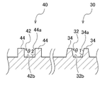
- FIG. 1A is a plan view of a master master 20 of one embodiment
- FIG. 2 is an enlarged view showing a part of the master master 20
- FIG. 2A is a plan view
- FIG. 2B is a cross-sectional view.
- the master master 20 is used to manufacture a metal molding by electroforming.
- the master master 20 has an electrodeposition surface 20a on which a metal molding is formed by electrodeposition.
- the master master 20 has, on the electrodeposition surface 20a, a product area 23 where a product portion cut out as a product from the metal molding is formed, and a non-product area 24 other than the product area 23.
- the master master 20 includes a product pattern 30 formed in the product region 23 and including recesses 32 and protrusions 34, and a plurality of recesses 42 and protrusions 44 formed in at least a part of the non-product region 24.
- the surface area of the product pattern 30 per unit area of the product region 23 is defined as the first surface area S1
- the surface area of the dummy pattern 40 per unit area of the dummy region 25 in which the dummy pattern 40 is formed is defined as S1.
- the pattern has a second surface area S2 larger than the first surface area S1.
- the product area 23 is, for example, an area surrounded by broken lines in the figure, and defined by alignment marks 31 in this example.
- three product areas 23 are provided around the center C of the electrodeposition surface 20a having a circular planar shape, with three-fold rotational symmetry. All areas other than the product area 23 on the electrodeposition surface 20 a are non-product areas 24 .
- the dummy area 25 is formed over substantially the entire non-product area 24 .
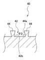
- Concavo-convex patterns including concavities and protrusions include concavo-convex patterns formed by forming concavities on a plane (hereinafter referred to as concavity patterns) and concavo-convex patterns formed by forming protrusions on a plane ( In the following, there is a convex pattern).
- concavity patterns concavo-convex patterns formed by forming concavities on a plane
- concavo-convex patterns formed by forming protrusions on a plane there is a convex pattern.
- FIG. 3 shows a partially enlarged plan view (FIG. 3A) and a cross-sectional view of the master master 20 when both the product patterns 30 and the dummy patterns 40 of the master master 20 are concave patterns. (Fig. 3B).
- the product pattern 30 may be a convex pattern
- the dummy pattern 40 may be a concave pattern.
- the uneven pattern includes a bottom surface and protrusions 34 and 44 protruding from the bottom surface.
- the bottom surface corresponds to the inner bottom surface of the recesses 32 and 42 (see FIGS. 2 and 3).
- the surface area of the product pattern 30 is the area of the product region 23 in plan view and the area of the sidewall 34a of the convex portion 34 of the product pattern 30. is the sum of
- the surface area of the product pattern 30 is the sum of the area of the product region 23 in plan view and the area of the sidewall 32a of the concave portion 32 of the product pattern 30. is.
- the surface area per unit area of the product pattern 30 is the average value of the surface area per unit area in each region.
- the surface area of the dummy pattern 40 is the sum of the area of the dummy region 25 in plan view and the area of the side wall 44a of the convex portion 44 of the dummy pattern 40. is.
- the surface area of the dummy pattern 40 is the sum of the area of the dummy region 25 in a plan view and the area of the side walls 42a of the recesses 42 of the dummy pattern 40. .
- the surface area per unit area of the dummy pattern 40 is the average value of the surface area per unit area in each region.
- the dummy area 25 is a closed area in which the dummy pattern 40 is formed within the non-product area 24 .
- dummy patterns 40 are formed over the entire non-product area 24 , and the entire non-product area 24 corresponds to the dummy area 25 .
- the dummy area 25 may be partially formed in the non-product area 24 as in the master master 120 shown in FIG. 1B.
- FIG. 1B the same reference numerals are given to the same components as those of the master disc 20 shown in FIGS. 1A and 2 . The same applies to the following drawings.
- a dummy pattern 40 is formed in a region surrounded by three product regions 23, and the region in which the dummy pattern 40 is formed is the dummy region 25.
- the dummy region 25 is formed on the plurality of convex portions 44 formed in the non-product region 24 . It is an area surrounding the outer periphery of the convex portion 44 located at the outermost portion.
- the dummy region 25 is the plurality of concave regions 42 formed in the non-product region 24 .
- the dummy area 25 is not limited to being provided at one place in the center of the master disc as shown in FIG. 1B, and may be provided anywhere within the non-product area 24. , may be formed in a plurality of locations.
- the size and density of the recesses or protrusions of the product pattern are determined by the product specifications and cannot be changed. If the surface area of the recesses or protrusions of the product pattern is small, the adhesion to the electrodeposition layer will be low, and there is a concern that peeling will occur between the electrodeposition layer and the master master during electroforming.
- JP-A-2015-30881 since dummy patterns are provided around product patterns, an anchor effect by the dummy patterns can also be expected.
- the dummy pattern disclosed in Japanese Patent Application Laid-Open No. 2015-30881 has smaller concave or convex dimensions than the product pattern.
- the anchor effect of the dummy pattern is smaller than the anchor effect of the product pattern, and the necessary anchor effect cannot be obtained.
- the surface area per unit area of the dummy area is larger than the surface area per unit area of the product area in the master disk 20, a high anchor effect can be exhibited, adhesion can be further improved, and electric It is possible to sufficiently exert the effect of suppressing the peeling during casting.
- the area of the dummy area 25 is larger than the area of the product area 23.
- the total area of all the dummy regions 25 formed in one master master 20 and 120 Compare with the total area of all product regions 23 .
- the area of one dummy area 25 is larger than the total area of the three product areas 23 . If the area of the dummy region 25 is larger than that of the product region 23, the anchor effect during electroforming is high, and the effect of suppressing peeling can be enhanced.
- a plurality of concave portions 42 or convex portions 44 are regularly arranged in the dummy area 25.
- the concave portions 42 and the convex portions 44 formed in the dummy region 25 are not limited to being arranged regularly, and may be arranged irregularly.
- the dummy pattern 40 may be a pattern in which irregular concave portions or convex portions are formed by roughening processing such as satin finish.
- the product pattern 30 includes at least one of the concave portions 32 and the convex portions 34, and the product pattern 30 includes the concave portions 32 or the convex portions 34 that are regularly arranged.
- the dummy pattern 40 also has a plurality of concave portions 42 and convex portions 44 arranged regularly.
- the arrangement pitch of the concave portions 42 or the convex portions 44 of the dummy pattern 40 is smaller than the arrangement pitch of the concave portions 32 or the convex portions 34 of the product pattern 30 . That is, in the dummy area 25 , the concave portions 42 or the convex portions 44 are preferably formed with a higher density than the arrangement density of the concave portions 32 or the convex portions 34 in the product region 23 . If the arrangement pitch of the concave portions 42 or the convex portions 44 of the dummy pattern 40 is smaller than the arrangement pitch of the concave portions 32 or the convex portions 34 of the product pattern 30, the second surface area S2 is easily made larger than the first surface area S1. can do
- the arrangement pitch of 34 is the average value of arrangement pitches Psa and Psb in respective directions of two orthogonal axes.
- the arrangement pitch of the protrusions 34 of the product pattern 30 is the arrangement pitch of the protrusions 34 in that one direction.
- the arrangement pitch of the concave portions 32 of the product pattern 30 is such that the convex portions 34 are replaced with the concave portions 32 in the above description.
- the arrangement pitch is the average value of arrangement pitches Pda and Pdb in respective directions of two orthogonal axes.
- the arrangement pitch of the protrusions 44 of the dummy pattern 40 is the arrangement pitch of the protrusions 44 in that one direction.
- the array pitch of the concave portions 42 of the dummy pattern 40 is such that the convex portions 44 are replaced with the concave portions 42 in the above description.
- the height Hd of the protrusions 44 of the dummy pattern 40 is higher than the height Hs of the protrusions 34 of the product pattern 30.
- Hd the height of the protrusions 44 of the dummy pattern 40
- Hs the height of the protrusions 34 of the product pattern 30.
- the aspect ratio of the protrusions 44 or recesses 42 of the dummy pattern 40 is preferably larger than the aspect ratio of the protrusions 34 or recesses 32 of the product pattern 30 .
- the second surface area S2 can be easily made larger than the first surface area S1.
- the aspect ratio is the height of the protrusion/the equivalent circle diameter of the area of the protrusion or the recess in plan view.
- Aspect ratio height Hs of convex portion 34/circular equivalent diameter Ds of area of convex portion 34 in plan view is.
- the dummy pattern 40 is a concave pattern
- Aspect ratio height Hs of convex portion 34/circular equivalent diameter Ds of area of concave portion 32 in plan view is.
- the dummy area 25 has recesses 42 or protrusions 44 that are larger in size than the recesses 32 or protrusions 34 in the product area 23 .
- the size larger than the concave portion 32 or the convex portion 34 in the product region 23 means that the product of the height Hd of the concave portion 42 or the convex portion 44 and the equivalent circle diameter Dd of the area in plan view is the height of the concave portion 32 or the convex portion 34 It is larger than the product of the height Hs and the circle-equivalent diameter Ds of the area in plan view. If the product region 23 includes concave portions 32 or convex portions 34 of different sizes, the height and the circle-equivalent diameter of the area in plan view are the average values thereof. The same is true when the dummy region 25 includes concave portions 42 or convex portions 44 of different sizes.
- the adhesion of the dummy pattern 40 to the electrodeposited layer during electroforming can be made higher than the adhesion of the product pattern 30, and the anchor effect of the dummy pattern 40 can be further enhanced. . Therefore, it is possible to enhance the effect of suppressing exfoliation of the metal molding during growth in the electroforming process.
- the angle ⁇ 2 between the side wall 44a of the projection 44 of the dummy pattern 40 and the bottom surface 42b of the recess 42 is preferably 90° or less.
- the master master 20 includes a conductive substrate 21 having an electrodeposition surface and a metal molding formed on the substrate 21. and a non-conductive mask to control material growth.
- the master master 20 has a convex pattern, and the convex portions 34 of the product pattern 30 and the convex portions 44 of the dummy pattern 40 are formed by a non-conductive mask. That is, the protrusions 34 of the product pattern 30 and the protrusions 44 of the dummy pattern 40 are made of a non-conductive material, and the protrusions 34 and 44 made of the non-conductive material inhibit the growth of the metal molding.
- the material of the non-conductive mask that forms at least one of the protrusions 34 of the product pattern 30 and the protrusions 44 of the dummy pattern 40 may be a photosensitive resin. Moreover, the material of the non-conductive mask that forms at least one of the protrusions 34 of the product pattern 30 and the protrusions 44 of the dummy pattern 40 may be an inorganic material.
- a metal substrate such as stainless steel is suitable for the conductive substrate 21 .
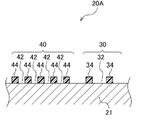
- a master master 20A shown in FIG. 7 includes a conductive substrate 21 and convex portions 34 and 44 as non-conductive masks on one surface of the substrate 21.
- the non-conductive mask protrusions 34 and 44 can be formed from a photosensitive resin.
- the master master 20A shown in FIG. 7 can be produced, for example, by forming a photosensitive resin layer on the substrate 21, exposing it in a mask pattern, and developing it. If both the product pattern 30 and the dummy pattern 40 are provided with the projections 34 and 44 made of a photosensitive resin layer, there is an advantage that the metal molding formed by electroforming can be easily separated from the master master 20A.
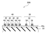
- the master master 20B shown in FIG. 8 includes a non-conductive substrate 22, a metal film 22a formed on one surface of the non-conductive substrate 22, and projections 34 and 44 as non-conductive masks on the metal film 22a. I have.
- the projections 34 and 44 are made of a photosensitive resin as in the master master 20A.
- a glass substrate, a silicon substrate, or the like can be used as the non-conductive substrate 22 .
- the flat substrate may be a conductive substrate or a non-conductive substrate without limitation.
- the master master 20C shown in FIG. 9 includes a conductive substrate 21 and projections 34 and 44 as non-conductive masks.
- the convex portions 34 and 44 which are non-conductive masks, can be made of an inorganic material instead of the photosensitive resin. Examples of inorganic materials include metal oxides, metal nitrides, and metal fluorides.
- a film is formed by sputtering or the like in a state in which a metal mask having an opening pattern corresponding to a desired convex pattern is arranged so as to face one surface of the substrate 21 . Thereby, the convex portions 34 and 44 can be formed according to the opening pattern.
- both the product pattern 30 and the dummy pattern 40 are provided with the projections 34 and 44 made of an inorganic material, even if the metal molding formed by electroforming is separated from the master master 20C, the uneven pattern of the master master 20C remains. be able to. Therefore, the master master 20C can be used repeatedly, and a plurality of metal moldings can be produced using one master master 20C.
- a master master 20D shown in FIG. 10 includes a conductive substrate 21 and projections 34 and 44 as non-conductive masks.
- the convex portions 34 of the product pattern 30 are made of a photosensitive resin
- the convex portions 44 of the dummy pattern 40 are made of an inorganic material. Since the protrusions 34 of the product pattern 30 are made of a photosensitive resin, the metal molding can be peeled off without applying a large load to the product portion.
- the projections 44 of the dummy pattern 40 are made of an inorganic material, they remain on the substrate 21 even after the metal molding is peeled off. Therefore, after the metal molding is peeled off, by forming only the projections 34 of the product pattern 30 again on the substrate 21, the master master 20D can be regenerated and used again for electroforming of the metal molding. It is possible.
- a master master 20E shown in FIG. 11 includes a conductive substrate 21 and convex portions 34 and 44 as non-conductive masks.
- the convex portions 34 of the product pattern 30 are made of an inorganic material
- the convex portions 44 of the dummy pattern 40 are made of a photosensitive resin. Since the projections 34 of the product pattern 30 are made of an inorganic material, they remain on the substrate 21 even after the metal molding is peeled off. Therefore, by forming only the projections 44 of the dummy pattern 40 again on the substrate 21 after peeling off the metal molding, the master master 20E can be regenerated and used again for electroforming of the metal molding. is.
- At least one of the protrusions 34 of the product pattern 30 and the protrusions 44 of the dummy pattern 40 may be made of a conductive material, and the other may be made of a non-conductive material. Specific aspects are shown in FIGS. 12 and 13. FIG.
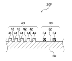
- a master master 20F shown in FIG. 12 is used when manufacturing a product having openings such as a nozzle plate, like the master masters 20A to 20E shown in FIGS.
- the master master 20F includes a metal substrate 28 integrally formed with the projections 44 of the dummy pattern 40 and the projections 34 of the product pattern 30 as a non-conductive mask.
- the convex portions 44 of the dummy pattern 40 are formed as part of the metal substrate 28.
- the protrusions 34 of the product pattern 30 are made of a non-conductive material.
- a photosensitive resin or an inorganic material can be used as the non-conductive material.
- metal oxides, metal nitrides or metal fluorides can be used in the same manner as described above.
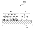
- the master master 20G shown in FIG. 13 includes a metal substrate 29 integrally formed with the projections 34 of the product pattern 30, and the projections 44 of the dummy pattern 40 as a non-conductive mask.
- the protrusions 34 of the product pattern 30 are formed as part of the metal substrate 29 .
- the projections 44 of the dummy pattern 40 are made of a non-conductive material.
- a photosensitive resin or an inorganic material can be used as the non-conductive material in the same manner as described above.
- both the concave portions 32 and the convex portions 34 forming the product pattern 30 in the product region 23 need to be conductive during electroforming.
- both the product pattern and the dummy pattern may have a non-conductive surface as the master master.
- conductivity may be imparted by forming a metal film on the non-conductive electrodeposited surface of the master master by sputtering or the like before electroforming. That is, the electrodeposited surface of the master master disk in the present disclosure includes a non-conductive aspect before being imparted with conductivity.
- a method of manufacturing a metal molding according to the present disclosure includes an electroforming process using a master disk.
- a metal molding is grown by depositing metal on the electroformed surface of the master master while the master is immersed in an electrolytic solution.
- the method for manufacturing a metal molded article includes a peeling step of peeling off the metal molded article from the master master disk.
- a metal molding is manufactured by performing the electroforming process and the peeling process.
- the method for manufacturing a metal molding according to the first embodiment will be described below.
- a method of manufacturing a nozzle plate 100 having a plurality of nozzles 102 as a metal molding will be described.
- FIG. 14 is a perspective view showing part of a nozzle plate 100 used in a recording head of an inkjet printer, which is an example of a metal molded product manufactured by the metal molded product manufacturing method of the first embodiment.
- the nozzle plate 100 is a plate-like member having a rectangular planar shape and made of an electroformed metal such as nickel (Ni).
- a plurality of substantially circular openings 102 functioning as nozzles (hereinafter referred to as nozzles 102 ) are formed in a two-dimensional array in the nozzle plate 100 .
- the nozzle 102 is formed in a substantially circular shape, and its diameter is, for example, 100 ⁇ m or less, preferably 20 ⁇ m to 50 ⁇ m.
- the nozzle plate 100 is arranged in such a posture that the longitudinal direction corresponds to the main scanning direction X of the inkjet printer and the short direction corresponds to the sub-scanning direction Y. As shown in FIG.
- the length of the nozzle plate 100 in the main scanning direction X is 100 mm as an example, and the length in the sub-scanning direction Y is 40 mm as an example.
- a master master 20A (see FIG. 7) having projections 34 and 44 made of a mask made of a non-conductive material on a conductive substrate 21 is used.
- the bottom surfaces of the concave portions 32 and 42 of the product pattern 30 and the dummy pattern 40 are the surface of the substrate 21, and the metal layer 101 that becomes the nozzle plate 100 grows from this portion.
- the growth of the metal layer 101 is suppressed in the portions of the mask made of non-conductive material (projections 34, 44). As a result, an opening is formed in the mask portion. This opening becomes the nozzle 102 in the nozzle plate 100 .
- the diameter DM of the convex portion 34 is larger than the diameter D of the nozzle 102, and is, for example, 150 ⁇ m to 200 ⁇ m. Further, the thickness of the convex portion 34 is, for example, 2 ⁇ m.
- FIG. 15A and 15B are diagrams showing the manufacturing process of the nozzle plate 100.
- FIG. FIG. 15 shows a partial cross section including only three protrusions 34 of product pattern 30 of master master 20 shown in FIG. 1A (S0).
- a metal layer 101 is grown as an electrodeposition layer on the electrodeposition surface 20a by a metal deposited from the electrolyte while the master plate 20 is immersed in the electrolyte.
- the metal layer 101 grows from the bottom surface of the concave portion 32, no metal is deposited on the surface of the convex portion 34, which is a non-conductive mask, and the metal layer 101 does not grow.
- a metal layer 101 gradually grows on the bottom surface of the recess 32 .
- the metal layer 101 grows from the surface of the previously grown metal layer 101 to the side of the protrusions 34 so as to cover the edges of the protrusions 34. do.
- an opening is formed in the metal layer 101 with the center position of the protrusion 34 as the center of the opening.
- This opening becomes the nozzle 102 .
- the metal layer 101 grows toward the center of the protrusion 34, so the opening diameter of the nozzle 102 gradually decreases.
- the diameter of the convex portion 34 is determined so that the nozzle 102 has a desired opening diameter when the metal layer 101 is grown to a desired thickness.
- the growth of the metal layer 101 on the convex portion 34 progresses closer to the bottom surface 32 b of the concave portion 32 . Therefore, as shown in FIG. 15, the opening diameter of the nozzle 102 becomes smaller as it approaches the bottom surface 32b and becomes larger as it moves away from the bottom surface 32b. .
- the opening diameter of the nozzle 102 closer to the bottom surface 32b is set. Then, the diameter of the convex portion 34 is determined so that the opening diameter of the nozzle 102 used as a reference becomes the target opening diameter.
- the thickness of the metal layer 101 is, for example, about 50 ⁇ m.
- the metal layer 101 is peeled off from the master master 20 (peeling process S2).
- the projections 34 made of the photosensitive resin are peeled off from the master master 20 (here, the substrate 21 ) together with the metal layer 101 .
- the protrusions 34 adhering to the metal layer 101 are removed (mask removing step S3). Further, the nozzle plate 100 can be obtained by punching out the product area 23 using the alignment marks 31 as marks.
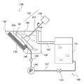
- FIG. 16 shows an example of an electroforming apparatus 130 used in the electroforming step S1.
- the electroforming apparatus 130 includes an electroforming bath 132 , a master holding mechanism 135 , an anode 139 , and a circulation mechanism 140 for the electrolytic solution 134 .
- the electroforming bath 132 stores the electrolytic solution 134 .
- An anode 139 is arranged on a part of the inner wall surface of the electroforming tank 132 .
- the master master 20 is immersed in the electrolytic solution 134 in the electroforming bath 132 .
- the master master 20 is arranged with the electrodeposition surface 20 a facing the anode 139 .
- the anode 139 contains electroformed metal such as nickel pellets, and has a size that allows it to face the entire electrodeposition surface 20 a on the master disc 20 . Electroforming to the master master 20 is performed with the electrodeposition surface 20a of the master master 20 and the anode 139 facing each other.
- the side wall of the electroforming tank 132 is partially inclined.
- the inclination direction of the sidewall is the direction in which the upper opening of the electroforming tank 132 is wider than the bottom surface of the electroforming tank 132 due to the inclination of the sidewall, and the inclination angle of the sidewall is, for example, about 40° to about 50° with respect to the horizontal direction.
- the anode 139 is arranged along the inner wall surface of the slanted side wall in a posture inclined with respect to the horizontal direction.
- the master disc holding mechanism 135 includes a holding portion 136 , a rotating shaft 137 and a rotating device 138 .
- the holding part 136 holds the master master 20 from the opposite side of the electrodeposition surface 20a of the master master 20 .
- the rotating shaft 137 is attached to the back surface of the holding portion 136 and extends in the normal direction of the back surface of the holding portion 136 .
- the rotating device 138 rotates the holding portion 136 via the rotating shaft 137 .
- the holding part 136 holds the master master 20 in the electroforming tank 132 so that the electrodeposition surface 20 a of the master master 20 faces the anode 139 . That is, the master disk 20 is arranged with the electrodeposition surface 20a tilted from the horizontal direction.
- the master disc 20 is held by the holding section 136 so that the center coincides with the rotating shaft 137 .
- the rotating device 138 is driven, the master disk 20 rotates integrally with the holding portion 136 via the rotating shaft 137 with the center coincident with the rotating shaft 137 as the center of rotation.
- the master master 20 is set on the holding portion 136 outside the electroforming bath 132 and is immersed in the electroforming bath 132 while being held by the holding portion 136 . Then, electroforming is performed while the master master 20 is rotated around an axis extending in the normal direction from the center position of the electrodeposition surface 20a.
- the electrodeposited surface 20a of the master master 20 is used as a cathode, and the electrodeposited surface 20a serving as the cathode and the anode 139 containing the electroformed metal are energized.
- the electroformed metal of the anode 139 is electrolyzed and dissolved into the electrolytic solution 134 as electric ions.
- the metal layer 101 is formed by electrodepositing the metal deposited from the electrolytic solution 134 on the electrodeposition surface 20a serving as the cathode.
- the circulation mechanism 140 includes a reservoir 141 , a discharge pipe 142 , a valve 143 , a pump 144 , a filter 146 , a supply pipe 147 and a nozzle 148 .
- the circulation mechanism 140 circulates the electrolytic solution 134 stored in the electroforming tank 132 between the electroforming tank 132 and a storage tank 141 arranged outside the electroforming tank 132 . This circulation causes the electrolytic solution 134 to flow between the electrodeposition surface 20 a and the anode 139 .
- the discharge pipe 142 and the supply pipe 147 constitute a circulation path for the electrolytic solution 134 between the electroforming tank 132 and the storage tank 141 .
- the discharge pipe 142 constitutes a return pipe for discharging the electrolytic solution 134 in the electroforming bath 132 and returning the discharged electrolytic solution 134 to the storage tank 141 in the circulation route.
- the supply pipe 147 constitutes a supply pipe line that supplies the electrolytic solution 134 from the storage tank 141 to the electroforming tank 132 in the circulation path.
- One end of the discharge pipe 142 is arranged inside the electroforming tank 132 and the other end is connected to the storage tank 141 .
- the discharge pipe 142 returns the electrolytic solution 134 exceeding a predetermined amount in the electroforming tank 132 to the storage tank 141 . Therefore, one end of the discharge pipe 142 is arranged at substantially the same height as the liquid level of the specified amount of the electrolytic solution 134 with the opening directed upward. As a result, the electrolytic solution 134 exceeding the specified amount in the electroforming tank 132 flows into the discharge pipe 142 and is returned to the storage tank 141 through the discharge pipe 142 .
- the supply pipe 147 also has one end located inside the electroforming tank 132 and the other end connected to the storage tank 141 .
- One end of the supply pipe 147 is connected to a nozzle 148 for injecting the electrolytic solution 134 into the electroforming bath 132 .
- the other end of the supply pipe 147 is connected to the bottom of the storage tank 141 .
- a valve 143 , a pump 144 , and a filter 146 are arranged in this order from the storage tank 141 side, which is the upstream side in the supply direction of the electrolytic solution 134 , on the supply pipe line formed by the supply pipe 147 .
- a valve 143 opens and closes the supply path.
- the circulation mechanism 140 is used to circulate the electrolytic solution 134 between the electroforming tank 132 and the storage tank 141 . Then, in the electroforming bath 132, the electrolyte 134 is sprayed from the nozzle 148 toward the space between the electrodeposition surface 20a and the anode 139, so that the fluid pressure of the electrolyte 134 is applied toward the electrodeposition surface 20a.
- the electrolytic solution 134 is made to flow to The electroforming step S1 is preferably performed while the electrolytic solution 134 is caused to flow in this manner. Electroforming is performed on the electrodeposition surface 20a of the master disk 20 as described above.
- the surface area per unit area of the dummy area 25 is larger than the surface area per unit area of the product area 23 . Therefore, in the electroforming process, the metal layer deposited on the electrodeposited surface 20a of the master master 20 can exhibit a high anchor effect, and the adhesion between the metal layer and the master master 20 can be further enhanced. can. Therefore, the effect of suppressing the separation of the metal layer from the master master 20 during electroforming can be sufficiently exhibited.
- the master master 20 has a water contact angle of 20° or less on the surface of the protrusions 34 of the product pattern 30 .
- the present inventor presumes the mechanism of poor molding of openings caused by air bubbles as follows.
- the metal layer grows to cover the edges of the mask while entraining the air bubbles.
- the metal layer containing the air bubbles expands more than other parts.
- the metal layer bulges from the edges of the mask toward the central portion.
- the size of the opening becomes smaller, or the shape of the opening, which should be circular, becomes crescent-shaped, which results in poor molding of the opening.
- the water contact angle of a general photosensitive resin layer is very large, for example, exceeds 80°.
- the surface of the master master 20 may be subjected to hydrophilic treatment.
- the method of hydrophilization treatment is not particularly limited, but oxygen plasma ashing treatment or ultraviolet ozone treatment is preferable.
- a photosensitive resin film 33 is formed on the surface of the substrate 21 by coating.
- a mask 36 for pattern formation is placed on the photosensitive resin film 33, and the photosensitive resin film 33 is pattern-exposed.
- the exposed photosensitive resin film 33 is developed and washed, thereby forming a master master disc having projections 34 made of photosensitive resin on the surface of the substrate 21, that is, a non-conductive mask. get 20.
- the electrodeposited surface 20a is subjected to a hydrophilization process S14.
- a hydrophilization treatment oxygen plasma ashing treatment or ultraviolet ozone treatment is performed.
- the master master 20 in which the water contact angle on the surface of the projections 34 is 20° or less. The water contact angle is measured using a contact angle meter, and the average value of 10 points is taken.
- the present inventors have found that when the oxygen plasma ashing treatment is applied as a hydrophilization treatment, the electrodeposited layer tends to peel off from the electrodeposited surface during electroforming.
- the master master 20 of the present disclosure by providing a dummy pattern separately from the product pattern, it is possible to suppress the separation of the metal layer deposited during electroforming from the master master 20.
- the surface area per unit area of the dummy area is larger than the surface area per unit area of the product area in the master disk 20, a high anchor effect can be exhibited, and adhesion can be further enhanced. Therefore, it is particularly effective when the electrodeposited surface 20a is subjected to a hydrophilic treatment by oxygen plasma ashing to prevent air bubbles from adhering to the master disk 20.
- a method for manufacturing a metal molding according to the second embodiment will be described.
- a method of manufacturing a metal mold 110 having a plurality of protrusions will be described as a metal molding.
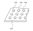
- FIG. 18 is a perspective view showing part of a metal mold 110, which is an example of a metal molded article produced by the method for manufacturing a metal molded article according to the second embodiment.
- the mold 110 is made of an electroformed metal such as Ni.
- a plurality of protrusions 112 are formed in a two-dimensional array on the mold 110 .
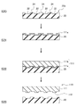
- FIG. 19 is a diagram showing the manufacturing process of the mold 110.
- the master master 20 includes product patterns and dummy patterns. showing.
- the master master 20 used in this example has a circular outer shape, but the outer shape is not limited to a circular one.
- the master master 20 indicated by S20 in FIG. 19 is made of a non-conductive substrate having a surface with an uneven pattern.
- a metal film 111a is formed on the electrodeposition surface 20a of the master master 20. As shown in FIG. This imparts electrical conductivity to the electrodeposition surface 20a.
- the metal layer 111b is grown on the metal film 111a by the metal deposited from the electrolyte while the master plate 20 is immersed in the electrolyte.
- the metal layer 111b grows on the bottom surfaces of the recesses 32 and 42 and the surfaces of the protrusions 34 and 44. If the metal material of the metal film 111a and the metal layer 111b is the same, the boundary between the two becomes indistinguishable, and the metal layer 111 is integrated.
- the metal layer 111 is peeled off from the master master 20 (peeling process S23).
- the metal layer 111 has an uneven pattern in which the product pattern and the dummy pattern formed on the electrodeposition surface of the master master 20 are transferred, and the mold 110 having the convex portions 112 shown in FIG. 19 is obtained.
- the master master disc 20 can exhibit a high anchoring effect. It is possible to suppress the occurrence of peeling of. In particular, in the case of a microchannel, etc., where the density of the uneven pattern in the product pattern is sparse, the adhesion between the master master and the electrodeposition layer in the product pattern is low, so a dummy pattern with a large surface area per unit area is provided. Thereby, a high effect of suppressing peeling can be obtained.
Abstract
In a master mold and a method for producing a metal molded article, the master mold has: a product region having an electrodeposition surface on which a metal molded article is formed by electrodeposition, in which a product part that is cut out as a product from the metal molded article is formed on the electrodeposition surface; and a non-product region other than the product region. The master mold has: a product pattern which is formed in the product region and includes a depressed part and a projecting part; and a dummy pattern which is formed in at least a part of the non-product region and includes a plurality of depressed parts and a plurality of projecting parts, in which, when the surface area of the product pattern per unit area of the product region is defined as a first surface area and the surface area of the dummy pattern per unit area of a dummy region on which the dummy pattern is formed is defined as a second surface area, the second surface area is larger than the first surface area.
Description
本開示は、電鋳用のマスター原盤及び金属成形物の製造方法に関する。
The present disclosure relates to a master master for electroforming and a method of manufacturing a metal molding.
凹凸を有する金属成形物を電鋳により製造するためのマスター原盤が知られている(例えば、特開2015-30881号公報参照)。このようなマスター原盤は、金属成形物が電着により形成される電着面を有し、かつ、電着面内に、例えばレジストによって凹凸パターンが形成される。電鋳の手順としては、凹凸パターンが形成されたマスター原盤をめっき液中に浸漬させた状態で、電着面に金属を析出させることにより金属成形物を成長させる。そして、成長した金属成形物をマスター原盤から剥離する。このようにして得られる金属成形物は、例えば、マスター原盤の凹凸パターンを反転した凹凸を有する。
A master master is known for manufacturing a metal molding having unevenness by electroforming (see, for example, Japanese Patent Application Laid-Open No. 2015-30881). Such a master disc has an electrodeposition surface on which a metal molding is formed by electrodeposition, and an uneven pattern is formed on the electrodeposition surface by, for example, a resist. As for the procedure of electroforming, a metal molding is grown by depositing metal on the electrodeposited surface while a master disk on which a concavo-convex pattern is formed is immersed in a plating solution. Then, the grown metal molding is peeled off from the master disk. The metal molding obtained in this manner has, for example, unevenness obtained by reversing the unevenness pattern of the master disc.
また、特開2015-30881号公報では、金属成形物として、インクジェットプリンタのインクを吐出させるノズルプレート、ろ過に利用されるフィルタプレートなど、複数の開口を有する開口プレートが挙げられている。
In addition, Japanese Patent Laid-Open No. 2015-30881 mentions an aperture plate having a plurality of apertures, such as a nozzle plate for ejecting ink for an inkjet printer and a filter plate used for filtration, as metal moldings.
特開2015-30881号公報には、開口プレートの開口を形成するためのプレート用の凹凸パターンの周囲に、プレート用の凹凸パターンよりも小さい寸法のダミーレジストパターンを形成したマスター原盤を用いることが開示されている。特開2015-30881号公報の技術によれば、プレート用の凹凸パターンの周囲にダミーパターンを備えたマスター原盤を用いて電鋳することにより、プレート用の凹凸パターンとその周囲の電流密度分布が均一化される。これにより、プレート用の凹凸パターンの全領域に形成される電着層の厚さを均一化することができる。
Japanese Patent Application Laid-Open No. 2015-30881 discloses that a master master disk in which a dummy resist pattern having a size smaller than that of the uneven pattern for the plate is formed around the uneven pattern for the plate for forming the openings of the aperture plate can be used. disclosed. According to the technique disclosed in Japanese Unexamined Patent Application Publication No. 2015-30881, electroforming is performed using a master master disk having a dummy pattern around the uneven pattern for the plate, so that the uneven pattern for the plate and the current density distribution around it are obtained. homogenized. As a result, the thickness of the electrodeposition layer formed over the entire area of the uneven pattern for the plate can be made uniform.
特開2015-30881号公報に記載されているように、マスター原盤によって形成される金属成形物は、マスター原盤から剥離された後、一部が製品として切り出される。このようなマスター原盤の電鋳面内には、金属成形物のうち製品として切り出される製品部分が形成される製品領域と、製品領域以外の非製品領域とが設けられる。特開2015-30881号公報において、製品領域は、プレート用の凹凸パターンなどの製品用パターンが形成される領域である。ダミーパターンは製品用パターンの周囲など、非製品領域の少なくとも一部に形成される。
As described in Japanese Patent Application Laid-Open No. 2015-30881, a metal molding formed by a master master is partly cut out as a product after being separated from the master master. In the electroformed surface of such a master disc, there are provided a product area where a product portion cut out as a product from the metal molding is formed, and a non-product area other than the product area. In Japanese Patent Application Laid-Open No. 2015-30881, the product area is an area in which product patterns such as uneven patterns for plates are formed. The dummy pattern is formed in at least part of the non-product area, such as around the product pattern.
特開2015-30881号公報のマスター原盤において、例えば、製品用パターンに含まれる凹部又は凸部の寸法が小さかったり、あるいは凹部又は凸部の密度が低い場合には、電鋳の途中で金属成形物がマスター原盤から剥離してしまう場合があった。
In the master master of JP-A-2015-30881, for example, if the dimensions of the recesses or protrusions included in the product pattern are small, or if the density of the recesses or protrusions is low, metal forming is performed during electroforming. In some cases, the object peeled off from the master disc.
本開示は、上記事情に鑑みてなされたものであり、電鋳工程において成長中の金属成形物の剥離を抑制することが可能なマスター原盤及び金属成形物の製造方法を提供することを目的とする。
The present disclosure has been made in view of the above circumstances, and aims to provide a master master and a method for manufacturing a metal molding that can suppress peeling of the metal molding during growth in the electroforming process. do.
本開示のマスター原盤は、金属成形物が電着により形成される電着面を有し、かつ、電着面において、金属成形物のうち製品として切り出される製品部分が形成される製品領域と、製品領域以外の非製品領域とを有するマスター原盤であって、
製品領域に形成され、凹部及び凸部を含む製品用パターンと、
非製品領域の少なくとも一部の領域に形成され、複数の凹部及び凸部を含むダミーパターンであって、製品領域の単位面積あたりの製品用パターンの表面積を第1表面積とし、ダミーパターンが形成されるダミー領域の単位面積あたりのダミーパターンの表面積を第2表面積とした場合において、第1表面積よりも第2表面積が大きいダミーパターンとを備えたマスター原盤である。 A master master disc of the present disclosure has an electrodeposition surface on which a metal molding is formed by electrodeposition, and a product region in which a product portion cut out as a product from the metal molding is formed on the electrodeposition surface, A master master having a non-product area other than the product area,
a product pattern formed in the product area and including recesses and protrusions;
A dummy pattern formed in at least a part of a non-product region and including a plurality of concave portions and convex portions, wherein the dummy pattern is formed with a surface area of the product pattern per unit area of the product region as a first surface area. and a dummy pattern having a second surface area larger than the first surface area, where the surface area of the dummy pattern per unit area of the dummy region is the second surface area.
本開示のマスター原盤においては、ダミー領域の面積が、製品領域よりも広いことが好ましい。
In the master disc of the present disclosure, it is preferable that the area of the dummy area is wider than the product area.
本開示のマスター原盤においては、ダミー領域において、複数の凹部又は凸部が規則的に配列されていることが好ましい。
In the master master disc of the present disclosure, it is preferable that a plurality of concave portions or convex portions are regularly arranged in the dummy area.
本開示のマスター原盤においては、製品用パターンが、凹部及び凸部の少なくとも一方を複数含み、製品用パターンにおいて、複数の凹部又は凸部が規則的に配列されており、
ダミーパターンの複数の凹部又は凸部の配列ピッチが製品用パターンの凹部又は凸部の配列ピッチよりも小さいことが好ましい。 In the master master disc of the present disclosure, the product pattern includes a plurality of at least one of concave portions and convex portions, and in the product pattern, the plurality of concave portions or convex portions are regularly arranged,
It is preferable that the arrangement pitch of the plurality of recesses or protrusions of the dummy pattern is smaller than the arrangement pitch of the recesses or protrusions of the product pattern.
本開示のマスター原盤においては、ダミーパターンの凸部の高さが、製品用パターンの凸部の高さよりも高いことが好ましい。
In the master master disk of the present disclosure, the height of the protrusions of the dummy pattern is preferably higher than the height of the protrusions of the product pattern.
本開示のマスター原盤においては、ダミーパターンの凸部又は凹部のアスペクト比が、製品用パターンの凸部又は凹部のアスペクト比よりも大きいことが好ましい。
In the master master disk of the present disclosure, it is preferable that the aspect ratio of the protrusions or recesses of the dummy pattern is larger than the aspect ratio of the protrusions or recesses of the product pattern.
本開示のマスター原盤においては、ダミーパターン及び製品用パターンは、それぞれ底面と底面から突出する凸部とを有しており、ダミーパターンの凸部の側壁と底面とのなす角が、製品用パターンの凸部の側壁と底面とのなす角よりも小さいことが好ましい。
In the master master disk of the present disclosure, the dummy pattern and the product pattern each have a bottom surface and a convex portion protruding from the bottom surface, and the angle formed by the side wall of the convex portion of the dummy pattern and the bottom surface is the product pattern. is preferably smaller than the angle formed by the side wall of the convex portion and the bottom surface.
本開示のマスター原盤においては、ダミーパターンは、底面と底面から突出する前記凸部とを有しており、ダミーパターンの凸部の側壁と底面とのなす角が、90°以下であることが好ましい。
In the master master disk of the present disclosure, the dummy pattern has a bottom surface and the convex portion protruding from the bottom surface, and the angle formed by the side wall of the convex portion of the dummy pattern and the bottom surface is 90° or less. preferable.
本開示のマスター原盤においては、電着面の平面形状は円形であり、電着面の中心に対して製品領域が3回回転対称に3つ設けられており、3つの製品領域に囲まれた領域内に、ダミーパターンが設けられていてもよい。
In the master master disk of the present disclosure, the planar shape of the electrodeposition surface is circular, and three product regions are provided with three-fold rotational symmetry with respect to the center of the electrodeposition surface. A dummy pattern may be provided in the region.
本開示のマスター原盤においては、電着面を有する導電性の基板と、電着面上に形成され金属成形物の成長を制御する非導電性のマスクとを有し、製品用パターン及びダミーパターンの凸部が非導電性のマスクであってもよい。
The master master disc of the present disclosure has a conductive substrate having an electrodeposited surface and a non-conductive mask formed on the electrodeposited surface to control the growth of a metal molding, and includes a product pattern and a dummy pattern. may be a non-conductive mask.
本開示のマスター原盤においては、製品用パターン及びダミーパターンの少なくとも一方の凸部を形成する非導電性のマスクの材料が感光性樹脂であってもよい。
In the master master disk of the present disclosure, the material of the non-conductive mask that forms the projections of at least one of the product pattern and the dummy pattern may be a photosensitive resin.
本開示のマスター原盤においては、製品用パターン及びダミーパターンの少なくとも一方の凸部を形成する非導電性のマスクの材料が無機材料であってもよい。
In the master master disc of the present disclosure, the material of the non-conductive mask that forms the projections of at least one of the product pattern and the dummy pattern may be an inorganic material.
本開示のマスター原盤においては、製品用パターンの凸部及びダミーパターンの凸部の少なくとも一方が導電性材料から形成されており、他方が非導電性材料から形成されていてもよい。
In the master master disc of the present disclosure, at least one of the convex portions of the product pattern and the convex portions of the dummy pattern may be made of a conductive material, and the other may be made of a non-conductive material.
本開示の金属成形物の製造方法は、本開示のマスター原盤を電鋳液中に浸漬した状態で、電着面に金属を析出させることにより金属成形物を成長させる電鋳工程と、マスター原盤から金属成形物を剥離する剥離工程とを含む。
The method for producing a metal molded product of the present disclosure includes an electroforming step of growing a metal molded product by depositing a metal on an electrodeposited surface while the master master of the present disclosure is immersed in an electroforming liquid; and a stripping step of stripping the metal molding from the.
本開示の金属成形物の製造方法においては、マスター原盤が、製品用パターンの凸部の表面の水接触角が20°以下であることが好ましい。
In the method for manufacturing a metal molded product of the present disclosure, it is preferable that the master disc has a water contact angle of 20° or less on the surface of the convex portions of the product pattern.
本開示のマスター原盤及び金属成形物の製造方法によれば、電鋳工程において成長中の金属成形物の剥離を抑制することが可能である。
According to the master master disk and the method for manufacturing a metal molded article of the present disclosure, it is possible to suppress the peeling of the growing metal molded article in the electroforming process.
以下、図面を参照して本開示の実施の形態について説明する。
Embodiments of the present disclosure will be described below with reference to the drawings.
「マスター原盤」
図1Aは一実施形態のマスター原盤20の平面図であり、図2は、マスター原盤20の一部を拡大して示す図であり、図2Aが平面図、図2Bが断面図である。 "Master original"
FIG. 1A is a plan view of amaster master 20 of one embodiment, FIG. 2 is an enlarged view showing a part of the master master 20, FIG. 2A is a plan view, and FIG. 2B is a cross-sectional view.
図1Aは一実施形態のマスター原盤20の平面図であり、図2は、マスター原盤20の一部を拡大して示す図であり、図2Aが平面図、図2Bが断面図である。 "Master original"
FIG. 1A is a plan view of a
マスター原盤20は、電鋳によって金属成形物を製造するために用いられる。マスター原盤20は、金属成形物が電着により形成される電着面20aを有する。マスター原盤20は、電着面20aにおいて、金属成形物のうち製品として切り出される製品部分が形成される製品領域23と、製品領域23以外の非製品領域24とを有する。さらに、マスター原盤20は、製品領域23に形成され、凹部32及び凸部34を含む製品用パターン30と、非製品領域24の少なくとも一部の領域に形成され、複数の凹部42及び凸部44を含むダミーパターン40とを含む。ここで、ダミーパターン40は、製品領域23の単位面積あたりの製品用パターン30の表面積を第1表面積S1とし、ダミーパターン40が形成されるダミー領域25の単位面積あたりのダミーパターン40の表面積を第2表面積S2とした場合において、第1表面積S1よりも第2表面積S2が大きいパターンである。
The master master 20 is used to manufacture a metal molding by electroforming. The master master 20 has an electrodeposition surface 20a on which a metal molding is formed by electrodeposition. The master master 20 has, on the electrodeposition surface 20a, a product area 23 where a product portion cut out as a product from the metal molding is formed, and a non-product area 24 other than the product area 23. As shown in FIG. Further, the master master 20 includes a product pattern 30 formed in the product region 23 and including recesses 32 and protrusions 34, and a plurality of recesses 42 and protrusions 44 formed in at least a part of the non-product region 24. and a dummy pattern 40 including Here, regarding the dummy pattern 40, the surface area of the product pattern 30 per unit area of the product region 23 is defined as the first surface area S1, and the surface area of the dummy pattern 40 per unit area of the dummy region 25 in which the dummy pattern 40 is formed is defined as S1. In the case of the second surface area S2, the pattern has a second surface area S2 larger than the first surface area S1.
製品領域23は、例えば、図中破線で囲われた領域であり、本例では、アライメントマーク31により規定される。本例のマスター原盤20では、平面形状が円形である電着面20aにおいて、電着面20aの中心Cの周りに製品領域23が3回回転対称に3つ設けられている。電着面20aにおいて、製品領域23以外の領域はすべて非製品領域24である。本例においては、ダミー領域25は、非製品領域24のほぼ全域にわたって形成されている。
The product area 23 is, for example, an area surrounded by broken lines in the figure, and defined by alignment marks 31 in this example. In the master disk 20 of this example, three product areas 23 are provided around the center C of the electrodeposition surface 20a having a circular planar shape, with three-fold rotational symmetry. All areas other than the product area 23 on the electrodeposition surface 20 a are non-product areas 24 . In this example, the dummy area 25 is formed over substantially the entire non-product area 24 .
凹部及び凸部を含む凹凸パターンには、平面に凹部が形成されることによって形成される凹凸パターン(以下において凹部型パターン)と、平面に凸部が形成されることによって形成される凹凸パターン(以下において凸部型パターン)とがある。図2に示すマスター原盤20は、製品用パターン30及びダミーパターン40の凹凸パターンのいずれもが凸部型パターンである。他方、図3には、マスター原盤20の製品用パターン30及びダミーパターン40の凹凸パターンのいずれもが凹部型パターンである場合の、マスター原盤20の一部拡大平面図(図3A)及び断面図(図3B)を示す。なお、製品用パターン30が凸部型パターン、ダミーパターン40が凹部型パターンなど、1つのマスター原盤20中に凸部型パターンと凹部型パターンとを含んでいてもよい。凹凸パターンが凸部型パターンであっても凹部型パターンであっても、凹凸パターンは底面と底面から突出する凸部34、44を含む。ここで、底面とは凹部32、42の内底面に相当する(図2、3参照)。
Concavo-convex patterns including concavities and protrusions include concavo-convex patterns formed by forming concavities on a plane (hereinafter referred to as concavity patterns) and concavo-convex patterns formed by forming protrusions on a plane ( In the following, there is a convex pattern). In the master master 20 shown in FIG. 2, both the product patterns 30 and the dummy patterns 40 are convex patterns. On the other hand, FIG. 3 shows a partially enlarged plan view (FIG. 3A) and a cross-sectional view of the master master 20 when both the product patterns 30 and the dummy patterns 40 of the master master 20 are concave patterns. (Fig. 3B). The product pattern 30 may be a convex pattern, and the dummy pattern 40 may be a concave pattern. Whether the uneven pattern is a convex pattern or a concave pattern, the uneven pattern includes a bottom surface and protrusions 34 and 44 protruding from the bottom surface. Here, the bottom surface corresponds to the inner bottom surface of the recesses 32 and 42 (see FIGS. 2 and 3).
製品用パターン30の表面積とは、製品領域23の平面視における面積Spと製品用パターン30の凹部32の側壁32aあるいは凸部34の側壁34aの面積Ss1の総和である。従って、製品用パターン30の単位面積当たりの表面積(第1表面積S1)は、S1=(Sp+Ss1)/Spで表される。
The surface area of the product pattern 30 is the sum of the area Sp of the product region 23 in plan view and the area Ss1 of the side wall 32a of the concave portion 32 or the side wall 34a of the convex portion 34 of the product pattern 30 . Therefore, the surface area (first surface area S1) per unit area of the product pattern 30 is represented by S1=(Sp+Ss1)/Sp.
図2に示すように、製品用パターン30が、凸部型パターンの場合、製品用パターン30の表面積は、製品領域23の平面視における面積と製品用パターン30の凸部34の側壁34aの面積の総和である。
As shown in FIG. 2, when the product pattern 30 is a convex pattern, the surface area of the product pattern 30 is the area of the product region 23 in plan view and the area of the sidewall 34a of the convex portion 34 of the product pattern 30. is the sum of
図3に示すように、製品用パターン30が、凹部型パターンの場合、製品用パターン30の表面積は、製品領域23の平面視における面積と製品用パターン30の凹部32の側壁32aの面積の総和である。
As shown in FIG. 3, when the product pattern 30 is a concave pattern, the surface area of the product pattern 30 is the sum of the area of the product region 23 in plan view and the area of the sidewall 32a of the concave portion 32 of the product pattern 30. is.
なお、図1Aのように製品領域23が複数ある場合には、製品用パターン30の単位面積当たりの表面積とは、それぞれの領域での単位面積当たりの表面積の平均値とする。
Note that when there are a plurality of product regions 23 as in FIG. 1A, the surface area per unit area of the product pattern 30 is the average value of the surface area per unit area in each region.
ダミーパターン40の表面積とは、ダミー領域25の平面視における面積Sdとダミーパターン40の凹部42の側壁42aあるいは凸部44の側壁44aの面積Ss2の総和である。従って、ダミーパターン40の単位面積当たりの表面積(第2表面積S2)は、S2=(Sd+Ss2)/Sdで表される。
The surface area of the dummy pattern 40 is the sum of the area Sd of the dummy region 25 in plan view and the area Ss2 of the side wall 42a of the concave portion 42 of the dummy pattern 40 or the side wall 44a of the convex portion 44 of the dummy pattern 40 . Therefore, the surface area (second surface area S2) per unit area of the dummy pattern 40 is represented by S2=(Sd+Ss2)/Sd.
図2に示すように、ダミーパターン40が、凸部型パターンである場合、ダミーパターン40の表面積は、ダミー領域25の平面視における面積とダミーパターン40の凸部44の側壁44aの面積の総和である。
As shown in FIG. 2, when the dummy pattern 40 is a convex pattern, the surface area of the dummy pattern 40 is the sum of the area of the dummy region 25 in plan view and the area of the side wall 44a of the convex portion 44 of the dummy pattern 40. is.
図3に示すように、ダミーパターン40が、凹部型パターンである場合、ダミーパターン40の表面積は、ダミー領域25の平面視における面積とダミーパターン40の凹部42の側壁42aの面積の総和である。
As shown in FIG. 3, when the dummy pattern 40 is a recessed pattern, the surface area of the dummy pattern 40 is the sum of the area of the dummy region 25 in a plan view and the area of the side walls 42a of the recesses 42 of the dummy pattern 40. .
なお、ダミー領域25が複数ある場合には、ダミーパターン40の単位面積当たりの表面積とは、それぞれの領域での単位面積当たりの表面積の平均値とする。
Note that when there are a plurality of dummy regions 25, the surface area per unit area of the dummy pattern 40 is the average value of the surface area per unit area in each region.
ダミー領域25は、非製品領域24内においてダミーパターン40が形成された閉領域をいう。図1Aに示すマスター原盤20においては、非製品領域24内の全域にわたってダミーパターン40が形成されており、非製品領域24全域がダミー領域25に相当する。図1Bに示すマスター原盤120のように、ダミー領域25は、非製品領域24に部分的に形成されていてもよい。図1Bにおいて、図1A及び図2に示すマスター原盤20の構成要素と同等の構成要素には同一の符号を付している。以下の図面においても同様とする。図1Bに示すマスター原盤120では、3つの製品領域23に囲まれた領域内に、ダミーパターン40が形成されており、このダミーパターン40が形成された領域がダミー領域25である。ダミーパターン40が凸部型パターンであって、ダミー領域25が非製品領域24に部分的に形成されている場合、ダミー領域25は、非製品領域24に形成されている複数の凸部44のうちの最外に位置する凸部44の外周を囲む領域である。また、ダミーパターン40が凹部型パターンであって、ダミー領域25が非製品領域24に部分的に形成されている場合、ダミー領域25とは、非製品領域24に形成されている複数の凹部42のうちの最外に位置する凹部42の外周を囲む領域である。なお、ダミー領域25は図1Bに示すようにマスター原盤の中央に1か所に設けられる態様に限らず非製品領域24内であれば、どこに設けられていてもよく、1か所に限らず、複数箇所に点在して形成されていてもよい。
The dummy area 25 is a closed area in which the dummy pattern 40 is formed within the non-product area 24 . In the master master disc 20 shown in FIG. 1A, dummy patterns 40 are formed over the entire non-product area 24 , and the entire non-product area 24 corresponds to the dummy area 25 . The dummy area 25 may be partially formed in the non-product area 24 as in the master master 120 shown in FIG. 1B. In FIG. 1B, the same reference numerals are given to the same components as those of the master disc 20 shown in FIGS. 1A and 2 . The same applies to the following drawings. In the master disc 120 shown in FIG. 1B, a dummy pattern 40 is formed in a region surrounded by three product regions 23, and the region in which the dummy pattern 40 is formed is the dummy region 25. When the dummy pattern 40 is a convex pattern and the dummy region 25 is partially formed in the non-product region 24 , the dummy region 25 is formed on the plurality of convex portions 44 formed in the non-product region 24 . It is an area surrounding the outer periphery of the convex portion 44 located at the outermost portion. Further, when the dummy pattern 40 is a concave pattern and the dummy region 25 is partially formed in the non-product region 24 , the dummy region 25 is the plurality of concave regions 42 formed in the non-product region 24 . It is a region surrounding the outer periphery of the concave portion 42 positioned at the outermost of the . Note that the dummy area 25 is not limited to being provided at one place in the center of the master disc as shown in FIG. 1B, and may be provided anywhere within the non-product area 24. , may be formed in a plurality of locations.
製品用パターンの凹部又は凸部のサイズ及び密度は、製品の仕様によって決まるため、変更することはできない。製品用パターンの凹部又は凸部の表面積が小さい場合、電着層との密着性が低くなり、電鋳時に電着層とマスター原盤との間で剥離が生じる懸念がある。特開2015-30881号公報には、製品用パターンの周囲にダミーパターンが設けられているため、ダミーパターンによるアンカー効果も期待できる。しかし、特開2015-30881号公報のダミーパターンは、製品用パターンよりも凹部又は凸部の寸法が小さい。そのため、製品用パターンのアンカー効果よりもダミーパターンのアンカー効果が小さく、必要なアンカー効果が得られない懸念があった。しかし、本マスター原盤20は、ダミー領域の単位面積当たりの表面積が製品領域の単位面積当たりの表面積よりも大きいので、高いアンカー効果を発揮させることができ、密着性をより高めることができ、電鋳時の剥離抑制効果を十分に発揮させることができる。
The size and density of the recesses or protrusions of the product pattern are determined by the product specifications and cannot be changed. If the surface area of the recesses or protrusions of the product pattern is small, the adhesion to the electrodeposition layer will be low, and there is a concern that peeling will occur between the electrodeposition layer and the master master during electroforming. In JP-A-2015-30881, since dummy patterns are provided around product patterns, an anchor effect by the dummy patterns can also be expected. However, the dummy pattern disclosed in Japanese Patent Application Laid-Open No. 2015-30881 has smaller concave or convex dimensions than the product pattern. Therefore, there is a concern that the anchor effect of the dummy pattern is smaller than the anchor effect of the product pattern, and the necessary anchor effect cannot be obtained. However, since the surface area per unit area of the dummy area is larger than the surface area per unit area of the product area in the master disk 20, a high anchor effect can be exhibited, adhesion can be further improved, and electric It is possible to sufficiently exert the effect of suppressing the peeling during casting.
マスター原盤20、120においては、ダミー領域25の面積が、製品領域23よりも広いことが好ましい。なお、マスター原盤20、120におけるダミー領域25の面積と製品領域23の面積とを比較する際には、1つのマスター原盤20、120中に形成されている全てのダミー領域25の総面積と、全ての製品領域23の総面積とを比較する。例えば、図1Bに示すマスター原盤120であれば、1つのダミー領域25の面積が、3つの製品領域23の総面積よりも広いことが好ましい。ダミー領域25の面積が製品領域23よりも広ければ、電鋳時におけるアンカー効果が高く、剥離抑制効果を高めることができる。
In the master discs 20 and 120, it is preferable that the area of the dummy area 25 is larger than the area of the product area 23. When comparing the area of the dummy regions 25 and the area of the product region 23 in the master masters 20 and 120, the total area of all the dummy regions 25 formed in one master master 20 and 120, Compare with the total area of all product regions 23 . For example, in the master master disc 120 shown in FIG. 1B, it is preferable that the area of one dummy area 25 is larger than the total area of the three product areas 23 . If the area of the dummy region 25 is larger than that of the product region 23, the anchor effect during electroforming is high, and the effect of suppressing peeling can be enhanced.
図1A、図2に示すマスター原盤20は、ダミー領域25において、複数の凹部42又は凸部44が規則的に配列されている。しかし、ダミー領域25に形成される凹部42及び凸部44は、規則的な配列に限らず、不規則に配列されていてもよい。また、ダミーパターン40は、梨地などの粗面化加工によって不規則な凹部又は凸部が形成されたパターンであってもよい。
In the master master disc 20 shown in FIGS. 1A and 2, a plurality of concave portions 42 or convex portions 44 are regularly arranged in the dummy area 25. As shown in FIG. However, the concave portions 42 and the convex portions 44 formed in the dummy region 25 are not limited to being arranged regularly, and may be arranged irregularly. Further, the dummy pattern 40 may be a pattern in which irregular concave portions or convex portions are formed by roughening processing such as satin finish.
本実施形態において、マスター原盤20においては、製品用パターン30が凹部32及び凸部34の少なくとも一方を複数含み、製品用パターン30において、複数の凹部32又は凸部34が規則的に配列されている。またダミーパターン40も、複数の凹部42及び凸部44が規則的に配列されている。
In the present embodiment, in the master master 20, the product pattern 30 includes at least one of the concave portions 32 and the convex portions 34, and the product pattern 30 includes the concave portions 32 or the convex portions 34 that are regularly arranged. there is The dummy pattern 40 also has a plurality of concave portions 42 and convex portions 44 arranged regularly.
このような場合、ダミーパターン40の凹部42又は凸部44の配列ピッチが製品用パターン30の凹部32又は凸部34の配列ピッチよりも小さいことが好ましい。すなわち、ダミー領域25においては、凹部42又は凸部44が製品領域23における凹部32又は凸部34の配置密度よりも高い密度で形成されていることが好ましい。ダミーパターン40の凹部42又は凸部44の配列ピッチが製品用パターン30の凹部32又は凸部34の配列ピッチよりも小さくすれば、容易に、第2表面積S2を第1表面積S1よりも大きくすることできる。
In such a case, it is preferable that the arrangement pitch of the concave portions 42 or the convex portions 44 of the dummy pattern 40 is smaller than the arrangement pitch of the concave portions 32 or the convex portions 34 of the product pattern 30 . That is, in the dummy area 25 , the concave portions 42 or the convex portions 44 are preferably formed with a higher density than the arrangement density of the concave portions 32 or the convex portions 34 in the product region 23 . If the arrangement pitch of the concave portions 42 or the convex portions 44 of the dummy pattern 40 is smaller than the arrangement pitch of the concave portions 32 or the convex portions 34 of the product pattern 30, the second surface area S2 is easily made larger than the first surface area S1. can do
製品用パターン30が凸部型パターンであって、図2に示すように、複数の凸部34が二次元状に互いに離隔して配列形成されたパターンである場合、製品用パターン30の凸部34の配列ピッチとは、直交する2軸のそれぞれの方向への配列ピッチPsa、Psbの平均値とする。複数の凸部34が一方向に互いに離隔して配列形成されたパターンである場合、製品用パターン30の凸部34の配列ピッチとは、その一方向への凸部34の配列ピッチである。
When the product pattern 30 is a convex pattern and, as shown in FIG. The arrangement pitch of 34 is the average value of arrangement pitches Psa and Psb in respective directions of two orthogonal axes. In the case of a pattern in which a plurality of protrusions 34 are arranged and formed in one direction while being separated from each other, the arrangement pitch of the protrusions 34 of the product pattern 30 is the arrangement pitch of the protrusions 34 in that one direction.
製品用パターン30が凹部型パターンである場合、製品用パターン30の凹部32の配列ピッチは、上記において凸部34を凹部32と読み替える。
When the product pattern 30 is a concave pattern, the arrangement pitch of the concave portions 32 of the product pattern 30 is such that the convex portions 34 are replaced with the concave portions 32 in the above description.
ダミーパターン40が凸部型パターンであって、図2に示すように、複数の凸部44が二次元状に互いに離隔して配列形成されたパターンである場合、ダミーパターン40の凸部44の配列ピッチとは、直交する2軸のそれぞれの方向への配列ピッチPda、Pdbの平均値とする。複数の凸部44が一方向に互いに離隔して配列形成されたパターンである場合、ダミーパターン40の凸部44の配列ピッチとは、その一方向への凸部44の配列ピッチである。
In the case where the dummy pattern 40 is a convex pattern, and as shown in FIG. The arrangement pitch is the average value of arrangement pitches Pda and Pdb in respective directions of two orthogonal axes. In the case of a pattern in which a plurality of protrusions 44 are arranged in one direction while being spaced apart from each other, the arrangement pitch of the protrusions 44 of the dummy pattern 40 is the arrangement pitch of the protrusions 44 in that one direction.
ダミーパターン40が凹部型パターンである場合、ダミーパターン40の凹部42の配列ピッチは、上記において凸部44を凹部42と読み替える。
When the dummy pattern 40 is a concave pattern, the array pitch of the concave portions 42 of the dummy pattern 40 is such that the convex portions 44 are replaced with the concave portions 42 in the above description.
マスター原盤20においては、図4に示すように、ダミーパターン40の凸部44の高さHdが、製品用パターン30の凸部34の高さHsよりも高いことが望ましい。Hd>Hsとすることにより、容易に、第2表面積S2を第1表面積S1よりも大きくすることできる。
In the master master 20, as shown in FIG. 4, it is desirable that the height Hd of the protrusions 44 of the dummy pattern 40 is higher than the height Hs of the protrusions 34 of the product pattern 30. By setting Hd>Hs, the second surface area S2 can be easily made larger than the first surface area S1.
マスター原盤20においては、ダミーパターン40の凸部44又は凹部42のアスペクト比が、製品用パターン30の凸部34又は凹部32のアスペクト比よりも大きいこと好ましい。ダミーパターン40の凹部42又は凸部44のアスペクト比を製品用パターン30の凹部32又は凸部34のアスペクト比よりも大きくすることにより、容易に、第2表面積S2を第1表面積S1よりも大きくすることできる。
In the master master 20 , the aspect ratio of the protrusions 44 or recesses 42 of the dummy pattern 40 is preferably larger than the aspect ratio of the protrusions 34 or recesses 32 of the product pattern 30 . By making the aspect ratio of the concave portion 42 or the convex portion 44 of the dummy pattern 40 larger than the aspect ratio of the concave portion 32 or the convex portion 34 of the product pattern 30, the second surface area S2 can be easily made larger than the first surface area S1. can do
ここで、アスペクト比は、凸部の高さ/凸部又は凹部の平面視における面積の円相当径である。例えば、製品用パターン30が凸部型パターンの場合、
アスペクト比=凸部34の高さHs/凸部34の平面視における面積の円相当径Ds
である。ダミーパターン40が凹部型パターンの場合、
アスペクト比=凸部34の高さHs/凹部32の平面視における面積の円相当径Ds
である。 Here, the aspect ratio is the height of the protrusion/the equivalent circle diameter of the area of the protrusion or the recess in plan view. For example, when theproduct pattern 30 is a convex pattern,
Aspect ratio=height Hs ofconvex portion 34/circular equivalent diameter Ds of area of convex portion 34 in plan view
is. When thedummy pattern 40 is a concave pattern,
Aspect ratio=height Hs ofconvex portion 34/circular equivalent diameter Ds of area of concave portion 32 in plan view
is.
アスペクト比=凸部34の高さHs/凸部34の平面視における面積の円相当径Ds
である。ダミーパターン40が凹部型パターンの場合、
アスペクト比=凸部34の高さHs/凹部32の平面視における面積の円相当径Ds
である。 Here, the aspect ratio is the height of the protrusion/the equivalent circle diameter of the area of the protrusion or the recess in plan view. For example, when the
Aspect ratio=height Hs of
is. When the
Aspect ratio=height Hs of
is.
同様に、ダミーパターン40が凸部型パターンの場合、
アスペクト比=凸部44の高さHd/凸部44の平面視における面積の円相当径Dd
である。また、ダミーパターン40が凹部型パターンの場合、
アスペクト比=凸部44の高さHd/凹部42の平面視における面積の円相当径Ddである。 Similarly, when thedummy pattern 40 is a convex pattern,
Aspect ratio=height Hd ofconvex portion 44/circle equivalent diameter Dd of area of convex portion 44 in plan view
is. Further, when thedummy pattern 40 is a concave pattern,
Aspect ratio=height Hd ofconvex portion 44/corresponding circle diameter Dd of area of concave portion 42 in plan view.
アスペクト比=凸部44の高さHd/凸部44の平面視における面積の円相当径Dd
である。また、ダミーパターン40が凹部型パターンの場合、
アスペクト比=凸部44の高さHd/凹部42の平面視における面積の円相当径Ddである。 Similarly, when the
Aspect ratio=height Hd of
is. Further, when the
Aspect ratio=height Hd of
ダミー領域25においては、製品領域23における凹部32又は凸部34よりも大きなサイズの凹部42又は凸部44を備えていることが好ましい。製品領域23における凹部32又は凸部34よりも大きなサイズとは、凹部42又は凸部44の高さHdと平面視における面積の円相当径Ddとの積が、凹部32又は凸部34の高さHsと平面視における面積の円相当径Dsとの積よりも大きいことを意味する。なお、製品領域23において異なるサイズの凹部32又は凸部34が含まれている場合には、高さ及び平面視における面積の円相当径はそれらの平均値とする。ダミー領域25において異なるサイズの凹部42又は凸部44が含まれている場合も同様である。
It is preferable that the dummy area 25 has recesses 42 or protrusions 44 that are larger in size than the recesses 32 or protrusions 34 in the product area 23 . The size larger than the concave portion 32 or the convex portion 34 in the product region 23 means that the product of the height Hd of the concave portion 42 or the convex portion 44 and the equivalent circle diameter Dd of the area in plan view is the height of the concave portion 32 or the convex portion 34 It is larger than the product of the height Hs and the circle-equivalent diameter Ds of the area in plan view. If the product region 23 includes concave portions 32 or convex portions 34 of different sizes, the height and the circle-equivalent diameter of the area in plan view are the average values thereof. The same is true when the dummy region 25 includes concave portions 42 or convex portions 44 of different sizes.
マスター原盤20においては、図5に示すように、ダミーパターン40の凸部44の側壁44aと凹部42の底面42bとのなす角θ2が、製品用パターン30の凸部34の側壁34aと凹部32の底面32bとのなす角θ1よりも小さいことが好ましい。θ2<θ1であることにより、電鋳時のダミーパターン40における電着層との密着性を製品用パターン30における密着性よりも高めることができ、ダミーパターン40によるアンカー効果をより高めることができる。従って、電鋳工程において成長中の金属成形物の剥離を抑制する効果を高めることができる。
In the master master 20, as shown in FIG. is preferably smaller than the angle θ1 formed with the bottom surface 32b. When θ2<θ1, the adhesion of the dummy pattern 40 to the electrodeposited layer during electroforming can be made higher than the adhesion of the product pattern 30, and the anchor effect of the dummy pattern 40 can be further enhanced. . Therefore, it is possible to enhance the effect of suppressing exfoliation of the metal molding during growth in the electroforming process.
なお、図6に示すように、ダミーパターン40の凸部44の側壁44aと凹部42の底面42bとのなす角θ2は、90°以下であることが好ましい。θ2を90°以下、より好ましくは90°未満とすることにより、電着時におけるダミーパターン40によるアンカー効果をさらに高めることができる。したがって、電鋳工程において成長中の金属成形物の剥離を抑制する効果をさらに高めることができる。
Incidentally, as shown in FIG. 6, the angle θ2 between the side wall 44a of the projection 44 of the dummy pattern 40 and the bottom surface 42b of the recess 42 is preferably 90° or less. By setting θ2 to 90° or less, more preferably less than 90°, the anchor effect of the dummy pattern 40 during electrodeposition can be further enhanced. Therefore, it is possible to further enhance the effect of suppressing exfoliation of the metal molding during growth in the electroforming process.
マスター原盤20の構成例20A~20Gについて図7~13を用いて説明する。
Configuration examples 20A to 20G of the master disc 20 will be described with reference to FIGS. 7 to 13. FIG.
金属成形物の製造方法については後述するが、ノズルプレートなどの開口を有する製品を製造する場合、マスター原盤20は、電着面を有する導電性の基板21と、基板21上に形成され金属成形物の成長を制御する非導電性のマスクとを備える。この場合、マスター原盤20は凸部型パターンを有し、製品用パターン30の凸部34及びダミーパターン40の凸部44が、非導電性マスクによって形成されている。すなわち、製品用パターン30の凸部34及びダミーパターン40の凸部44が、非導電性材料から構成されており、非導電性材料からなる凸部34及び凸部44が金属成形物の成長を制御する非導電性のマスクとして機能する。なお、製品用パターン30の凸部34及びダミーパターン40の凸部44の少なくとも一方を形成する非導電性のマスクの材料は感光性樹脂であってもよい。また、製品用パターン30の凸部34及びダミーパターン40の凸部44の少なくとも一方を形成する非導電性のマスクの材料は無機材料であってもよい。導電性の基板21としてはステンレス鋼などの金属基板が好適である。
A method for manufacturing a metal molding will be described later, but when manufacturing a product having an opening such as a nozzle plate, the master master 20 includes a conductive substrate 21 having an electrodeposition surface and a metal molding formed on the substrate 21. and a non-conductive mask to control material growth. In this case, the master master 20 has a convex pattern, and the convex portions 34 of the product pattern 30 and the convex portions 44 of the dummy pattern 40 are formed by a non-conductive mask. That is, the protrusions 34 of the product pattern 30 and the protrusions 44 of the dummy pattern 40 are made of a non-conductive material, and the protrusions 34 and 44 made of the non-conductive material inhibit the growth of the metal molding. Acts as a controlling non-conducting mask. The material of the non-conductive mask that forms at least one of the protrusions 34 of the product pattern 30 and the protrusions 44 of the dummy pattern 40 may be a photosensitive resin. Moreover, the material of the non-conductive mask that forms at least one of the protrusions 34 of the product pattern 30 and the protrusions 44 of the dummy pattern 40 may be an inorganic material. A metal substrate such as stainless steel is suitable for the conductive substrate 21 .
図7に示すマスター原盤20Aは、導電性の基板21と、基板21の一面に非導電性のマスクとしての凸部34、44を備えている。非導電性のマスクである凸部34及び44は感光性樹脂から形成することができる。図7に示すマスター原盤20Aは、例えば、基板21上に感光性樹脂層を形成し、マスクパターン状に露光し、現像することで作製することができる。製品用パターン30及びダミーパターン40いずれも感光性樹脂層からなる凸部34、44を備えた場合、電鋳により形成された金属成形物をマスター原盤20Aから剥離しやすいというメリットがある。
A master master 20A shown in FIG. 7 includes a conductive substrate 21 and convex portions 34 and 44 as non-conductive masks on one surface of the substrate 21. The non-conductive mask protrusions 34 and 44 can be formed from a photosensitive resin. The master master 20A shown in FIG. 7 can be produced, for example, by forming a photosensitive resin layer on the substrate 21, exposing it in a mask pattern, and developing it. If both the product pattern 30 and the dummy pattern 40 are provided with the projections 34 and 44 made of a photosensitive resin layer, there is an advantage that the metal molding formed by electroforming can be easily separated from the master master 20A.
図8に示すマスター原盤20Bは、非導電性基板22と、非導電性基板22の一面に形成された金属膜22aと、金属膜22a上に非導電性のマスクとしての凸部34、44を備えている。マスター原盤20Aと同様に凸部34、44は感光性樹脂から形成されている。非導電性基板22としては、ガラス基板あるいはシリコン基板などを用いることができる。このように、平板基板としては、導電性基板であっても、非導電性基板であっても制限なく用いることができる。
The master master 20B shown in FIG. 8 includes a non-conductive substrate 22, a metal film 22a formed on one surface of the non-conductive substrate 22, and projections 34 and 44 as non-conductive masks on the metal film 22a. I have. The projections 34 and 44 are made of a photosensitive resin as in the master master 20A. A glass substrate, a silicon substrate, or the like can be used as the non-conductive substrate 22 . As described above, the flat substrate may be a conductive substrate or a non-conductive substrate without limitation.
図9に示すマスター原盤20Cは、マスター原盤20Aと同様に、導電性の基板21と、非導電性のマスクとしての凸部34、44を備えている。非導電性のマスクである凸部34、44は感光性樹脂に代えて無機材料から形成することができる。無機材料としては、金属酸化物、金属窒化物あるいは金属フッ化物などが挙げられる。図9に示すマスター原盤20Cは、例えば、基板21の一面に対向させて、所望の凸部型パターンに応じた開口パターンを有する金属マスクを配置した状態で、スパッタ等による成膜を行う。これによって、開口パターンに応じた凸部34、44を形成することができる。製品用パターン30及びダミーパターン40いずれも無機材料からなる凸部34、44を備えた場合、電鋳により形成された金属成形物をマスター原盤20Cから剥離してもマスター原盤20Cの凹凸パターンを残すことができる。従って、マスター原盤20Cを繰り返し利用することが可能であり、1つのマスター原盤20Cを用いて複数の金属成形物を作製することができる。
Like the master master 20A, the master master 20C shown in FIG. 9 includes a conductive substrate 21 and projections 34 and 44 as non-conductive masks. The convex portions 34 and 44, which are non-conductive masks, can be made of an inorganic material instead of the photosensitive resin. Examples of inorganic materials include metal oxides, metal nitrides, and metal fluorides. For the master master 20C shown in FIG. 9, for example, a film is formed by sputtering or the like in a state in which a metal mask having an opening pattern corresponding to a desired convex pattern is arranged so as to face one surface of the substrate 21 . Thereby, the convex portions 34 and 44 can be formed according to the opening pattern. When both the product pattern 30 and the dummy pattern 40 are provided with the projections 34 and 44 made of an inorganic material, even if the metal molding formed by electroforming is separated from the master master 20C, the uneven pattern of the master master 20C remains. be able to. Therefore, the master master 20C can be used repeatedly, and a plurality of metal moldings can be produced using one master master 20C.
図10に示すマスター原盤20Dは、導電性の基板21と、非導電性のマスクとしての凸部34、44を備えている。マスター原盤20Dにおいては、製品用パターン30の凸部34が感光性樹脂により形成され、ダミーパターン40の凸部44が無機材料により形成されている。製品用パターン30の凸部34が感光性樹脂であるので、金属成形物を剥離する際、製品部分に大きな負荷をかけることなく剥離することができる。一方、ダミーパターン40の凸部44は無機材料で形成されているので、金属成形物剥離後も基板21上に残留する。そのため、金属成形物剥離後、基板21上に製品用パターン30の凸部34のみを再度形成することにより、マスター原盤20Dを再生することができ、再び、金属成形物の電鋳に用いることが可能である。
A master master 20D shown in FIG. 10 includes a conductive substrate 21 and projections 34 and 44 as non-conductive masks. In the master master 20D, the convex portions 34 of the product pattern 30 are made of a photosensitive resin, and the convex portions 44 of the dummy pattern 40 are made of an inorganic material. Since the protrusions 34 of the product pattern 30 are made of a photosensitive resin, the metal molding can be peeled off without applying a large load to the product portion. On the other hand, since the projections 44 of the dummy pattern 40 are made of an inorganic material, they remain on the substrate 21 even after the metal molding is peeled off. Therefore, after the metal molding is peeled off, by forming only the projections 34 of the product pattern 30 again on the substrate 21, the master master 20D can be regenerated and used again for electroforming of the metal molding. It is possible.
図11に示すマスター原盤20Eは、導電性の基板21と、非導電性のマスクとしての凸部34、44とを備えている。マスター原盤20Eにおいては、製品用パターン30の凸部34が無機材料により形成され、ダミーパターン40の凸部44が感光性樹脂により形成されている。製品用パターン30の凸部34は無機材料で形成されているので、金属成形物剥離後も基板21上に残留する。そのため、金属成形物剥離後、基板21上にダミーパターン40の凸部44のみを再度形成することにより、マスター原盤20Eを再生することができ、再び、金属成形物の電鋳に用いることが可能である。
A master master 20E shown in FIG. 11 includes a conductive substrate 21 and convex portions 34 and 44 as non-conductive masks. In the master master 20E, the convex portions 34 of the product pattern 30 are made of an inorganic material, and the convex portions 44 of the dummy pattern 40 are made of a photosensitive resin. Since the projections 34 of the product pattern 30 are made of an inorganic material, they remain on the substrate 21 even after the metal molding is peeled off. Therefore, by forming only the projections 44 of the dummy pattern 40 again on the substrate 21 after peeling off the metal molding, the master master 20E can be regenerated and used again for electroforming of the metal molding. is.
また、マスター原盤20は、製品用パターン30の凸部34及びダミーパターン40の凸部44の少なくとも一方が導電性材料から形成されており、他方が非導電性材料から形成されていてもよい。具体的な態様を図12及び図13に示す。
Further, in the master master 20, at least one of the protrusions 34 of the product pattern 30 and the protrusions 44 of the dummy pattern 40 may be made of a conductive material, and the other may be made of a non-conductive material. Specific aspects are shown in FIGS. 12 and 13. FIG.
図12に示すマスター原盤20Fは、図7~図11に示したマスター原盤20A~20Eと同様に、ノズルプレートなどの開口を有する製品を製造する場合に用いられる。マスター原盤20Fは、ダミーパターン40の凸部44が一体的に形成された金属基板28と、非導電性のマスクとしての製品用パターン30の凸部34とを備えている。マスター原盤20Fにおいて、ダミーパターン40の凸部44は金属基板28の一部として形成されている。そして、製品用パターン30の凸部34が非導電性材料により形成されている。非導電性材料としては、感光性樹脂あるいは無機材料を用いることができる。無機材料としては、上記と同様に金属酸化物、金属窒化物あるいは金属フッ化物を用いることができる。
A master master 20F shown in FIG. 12 is used when manufacturing a product having openings such as a nozzle plate, like the master masters 20A to 20E shown in FIGS. The master master 20F includes a metal substrate 28 integrally formed with the projections 44 of the dummy pattern 40 and the projections 34 of the product pattern 30 as a non-conductive mask. In the master disc 20F, the convex portions 44 of the dummy pattern 40 are formed as part of the metal substrate 28. As shown in FIG. The protrusions 34 of the product pattern 30 are made of a non-conductive material. A photosensitive resin or an inorganic material can be used as the non-conductive material. As the inorganic material, metal oxides, metal nitrides or metal fluorides can be used in the same manner as described above.
一方、製品がインプリント用のスタンパ等の金型である場合は、電鋳時において、製品領域23の製品用パターン30を形成する凹部32及び凸部34はいずれも導電性を有する必要がある。図13に示すマスター原盤20Gは、製品用パターン30の凸部34が一体的に形成された金属基板29と、非導電性のマスクとしてのダミーパターン40の凸部44とを備えている。マスター原盤20Gにおいて、製品用パターン30の凸部34は金属基板29の一部として形成されている。本例において、ダミーパターン40の凸部44が非導電性材料により形成されている。非導電性材料としては、上記と同様に、感光性樹脂あるいは無機材料を用いることができる。
On the other hand, when the product is a mold such as a stamper for imprinting, both the concave portions 32 and the convex portions 34 forming the product pattern 30 in the product region 23 need to be conductive during electroforming. . The master master 20G shown in FIG. 13 includes a metal substrate 29 integrally formed with the projections 34 of the product pattern 30, and the projections 44 of the dummy pattern 40 as a non-conductive mask. In the master master disc 20G, the protrusions 34 of the product pattern 30 are formed as part of the metal substrate 29 . In this example, the projections 44 of the dummy pattern 40 are made of a non-conductive material. A photosensitive resin or an inorganic material can be used as the non-conductive material in the same manner as described above.
なお、金型用のマスター原盤の場合、既述の通り、電鋳時において、製品領域23の製品用パターン30を形成する凹部32及び凸部34はいずれも導電性を有する必要がある。しかし、マスター原盤としては、製品用パターン及びダミーパターンのいずれも非導電性の表面を有するものであってよい。この場合、電鋳前にマスター原盤の非導電性の電着面にスパッタ等により金属膜を形成して導電性を付与すればよい。すなわち、本開示におけるマスター原盤における電着面とは、導電性が付与される前の非導電性である態様を含むものとする。
In the case of a master master disk for a mold, as described above, both the concave portions 32 and the convex portions 34 forming the product pattern 30 in the product region 23 need to be conductive during electroforming. However, both the product pattern and the dummy pattern may have a non-conductive surface as the master master. In this case, conductivity may be imparted by forming a metal film on the non-conductive electrodeposited surface of the master master by sputtering or the like before electroforming. That is, the electrodeposited surface of the master master disk in the present disclosure includes a non-conductive aspect before being imparted with conductivity.
「金属成形物の製造方法」
次に、本開示のマスター原盤を用いた金属成形物の製造方法について説明する。本開示の金属成形物製造方法は、マスター原盤を用いた電鋳工程を含む。電鋳工程では、マスター原盤を電解液中に浸漬させた状態で、マスター原盤の電鋳面に金属を析出させることにより金属成形物を成長させる。さらに、金属成形物の製造方法は、マスター原盤から金属成形物を剥離する剥離工程を含む。この電鋳工程及び剥離工程を実行することにより金属成形物を製造する。 "Manufacturing method of metal molding"
Next, a method for manufacturing a metal molding using the master master of the present disclosure will be described. A method of manufacturing a metal molding according to the present disclosure includes an electroforming process using a master disk. In the electroforming process, a metal molding is grown by depositing metal on the electroformed surface of the master master while the master is immersed in an electrolytic solution. Furthermore, the method for manufacturing a metal molded article includes a peeling step of peeling off the metal molded article from the master master disk. A metal molding is manufactured by performing the electroforming process and the peeling process.
以下に、第1の実施形態の金属成形物製造方法を説明する。ここでは、金属成形物として、複数のノズル102を有するノズルプレート100についての製造方法を説明する。
The method for manufacturing a metal molding according to the first embodiment will be described below. Here, a method of manufacturing a nozzle plate 100 having a plurality of nozzles 102 as a metal molding will be described.
図14は、第1の実施形態の金属成形物の製造方法によって作製される金属成形物の一例である、インクジェットプリンタの記録ヘッドに用いられるノズルプレート100の一部を示す斜視図である。
FIG. 14 is a perspective view showing part of a nozzle plate 100 used in a recording head of an inkjet printer, which is an example of a metal molded product manufactured by the metal molded product manufacturing method of the first embodiment.
ノズルプレート100はニッケル(Ni)等の電鋳金属で形成された、平面形状が矩形の板状部材である。ノズルプレート100には、ノズルとして機能する略円形の複数の開口102(以下においてノズル102という。)が二次元状に配列形成されている。ノズル102は略円形に形成されており、その直径は、例えば100μm以下であり、好ましくは20μm~50μmである。記録ヘッドにおいて、ノズルプレート100は長尺方向がインクジェットプリンタの主走査方向Xに、短尺方向が副走査方向Yに対応する姿勢で配置される。ノズルプレート100の主走査方向Xの長さは一例として100mm、副走査方向Yの長さは一例として40mmである。
The nozzle plate 100 is a plate-like member having a rectangular planar shape and made of an electroformed metal such as nickel (Ni). A plurality of substantially circular openings 102 functioning as nozzles (hereinafter referred to as nozzles 102 ) are formed in a two-dimensional array in the nozzle plate 100 . The nozzle 102 is formed in a substantially circular shape, and its diameter is, for example, 100 μm or less, preferably 20 μm to 50 μm. In the recording head, the nozzle plate 100 is arranged in such a posture that the longitudinal direction corresponds to the main scanning direction X of the inkjet printer and the short direction corresponds to the sub-scanning direction Y. As shown in FIG. The length of the nozzle plate 100 in the main scanning direction X is 100 mm as an example, and the length in the sub-scanning direction Y is 40 mm as an example.
マスター原盤20としては、一例として、導電性の基板21上に非導電性材料により形成されたマスクからなる凸部34、44を有するマスター原盤20A(図7参照)を用いる。マスター原盤20において、製品用パターン30及びダミーパターン40の凹部32、42の底面が基板21の表面であり、この部分からノズルプレート100となる金属層101が成長する。非導電性材料からなるマスクの部分(凸部34、44)では、金属層101の成長が抑制される。その結果としてマスクの部分に開口が形成されることとなる。この開口がノズルプレート100におけるノズル102となる。本例では、上述したノズルプレート100のノズル102の配列ピッチ及び数に対応して、マスター原盤20の100mm×40mmの領域に、4列に配列された凸部34が形成されている。凸部34の直径DMは、ノズル102の直径Dより大きく、例えば、150μm~200μmである。また、凸部34の厚みは、一例として、2μmである。
As an example of the master master 20, a master master 20A (see FIG. 7) having projections 34 and 44 made of a mask made of a non-conductive material on a conductive substrate 21 is used. In the master master 20, the bottom surfaces of the concave portions 32 and 42 of the product pattern 30 and the dummy pattern 40 are the surface of the substrate 21, and the metal layer 101 that becomes the nozzle plate 100 grows from this portion. The growth of the metal layer 101 is suppressed in the portions of the mask made of non-conductive material (projections 34, 44). As a result, an opening is formed in the mask portion. This opening becomes the nozzle 102 in the nozzle plate 100 . In this example, four rows of projections 34 are formed in a 100 mm×40 mm area of the master disc 20 corresponding to the arrangement pitch and number of the nozzles 102 of the nozzle plate 100 described above. The diameter DM of the convex portion 34 is larger than the diameter D of the nozzle 102, and is, for example, 150 μm to 200 μm. Further, the thickness of the convex portion 34 is, for example, 2 μm.
図15はノズルプレート100の製造工程を示す図である。図15においては、図1Aに示すマスター原盤20の製品用パターン30の凸部34を3つだけ含む一部断面を示している(S0)。まず、電鋳工程S1において、マスター原盤20を電解液中に浸漬させた状態で、電解液中から析出する金属によって電着面20aに電着層として金属層101を成長させる。
15A and 15B are diagrams showing the manufacturing process of the nozzle plate 100. FIG. FIG. 15 shows a partial cross section including only three protrusions 34 of product pattern 30 of master master 20 shown in FIG. 1A (S0). First, in an electroforming step S1, a metal layer 101 is grown as an electrodeposition layer on the electrodeposition surface 20a by a metal deposited from the electrolyte while the master plate 20 is immersed in the electrolyte.
電鋳の際、凹部32の底面から金属層101が成長する一方、非導電性のマスクである凸部34の表面には金属が析出されず、金属層101は成長しない。金属層101は凹部32の底面上で徐々に成長する。その後、成長した金属層101の厚みが凸部34の厚みを超えると、先に成長した金属層101の表面から凸部34側にも凸部34の縁部に被さるように金属層101が成長する。凸部34の縁部から中央に向かって金属層101が成長することにより、金属層101には、凸部34のほぼ中央位置を開口中心とする開口が形成される。この開口がノズル102となる。金属層101の厚みが増すと、金属層101は凸部34の中央に向かって成長するため、ノズル102の開口径も徐々に小さくなっていく。金属層101を所望の厚みまで成長させたときに、ノズル102が所望の開口径となるように、凸部34の径が決定されている。凸部34上において、金属層101の成長は、凹部32の底面32bに近いほど進む。そのため、図15に示すように、ノズル102の開口径は、底面32bに近いほど小さく、底面32bから離れるほど大きくなり、ノズル102の内壁面を構成する金属層101の断面は、円弧状となる。例えば、目標となるノズル102の開口径の基準は、底面32bに近い方のノズル102の開口径が設定される。そして、基準としたノズル102の開口径が目標の開口径となるように、凸部34の径が決定される。金属層101の厚さは、一例として50μm程度である。
During electroforming, while the metal layer 101 grows from the bottom surface of the concave portion 32, no metal is deposited on the surface of the convex portion 34, which is a non-conductive mask, and the metal layer 101 does not grow. A metal layer 101 gradually grows on the bottom surface of the recess 32 . After that, when the thickness of the grown metal layer 101 exceeds the thickness of the protrusions 34, the metal layer 101 grows from the surface of the previously grown metal layer 101 to the side of the protrusions 34 so as to cover the edges of the protrusions 34. do. As the metal layer 101 grows from the edges of the protrusions 34 toward the center, an opening is formed in the metal layer 101 with the center position of the protrusion 34 as the center of the opening. This opening becomes the nozzle 102 . As the thickness of the metal layer 101 increases, the metal layer 101 grows toward the center of the protrusion 34, so the opening diameter of the nozzle 102 gradually decreases. The diameter of the convex portion 34 is determined so that the nozzle 102 has a desired opening diameter when the metal layer 101 is grown to a desired thickness. The growth of the metal layer 101 on the convex portion 34 progresses closer to the bottom surface 32 b of the concave portion 32 . Therefore, as shown in FIG. 15, the opening diameter of the nozzle 102 becomes smaller as it approaches the bottom surface 32b and becomes larger as it moves away from the bottom surface 32b. . For example, as a reference for the target opening diameter of the nozzle 102, the opening diameter of the nozzle 102 closer to the bottom surface 32b is set. Then, the diameter of the convex portion 34 is determined so that the opening diameter of the nozzle 102 used as a reference becomes the target opening diameter. The thickness of the metal layer 101 is, for example, about 50 μm.
電鋳工程の後、金属層101をマスター原盤20から剥離する(剥離工程S2)。この際、感光性樹脂からなる凸部34は金属層101と共にマスター原盤20(ここでは、基板21)から剥離される。
After the electroforming process, the metal layer 101 is peeled off from the master master 20 (peeling process S2). At this time, the projections 34 made of the photosensitive resin are peeled off from the master master 20 (here, the substrate 21 ) together with the metal layer 101 .
その後、金属層101に付着した凸部34を除去する(マスク除去工程S3)。さらに、アライメントマーク31を目印に製品領域23を打ち抜くことによって、ノズルプレート100を得ることができる。
After that, the protrusions 34 adhering to the metal layer 101 are removed (mask removing step S3). Further, the nozzle plate 100 can be obtained by punching out the product area 23 using the alignment marks 31 as marks.
上記電鋳工程S1の詳細について説明する。図16は、電鋳工程S1において用いられる電鋳装置130の一例を示す。電鋳装置130は、電鋳槽132と、原盤保持機構135と、陽極139と、電解液134の循環機構140とを備えている。
The details of the electroforming step S1 will be described. FIG. 16 shows an example of an electroforming apparatus 130 used in the electroforming step S1. The electroforming apparatus 130 includes an electroforming bath 132 , a master holding mechanism 135 , an anode 139 , and a circulation mechanism 140 for the electrolytic solution 134 .
電鋳槽132は電解液134を貯留する。電鋳槽132の内壁面の一部には陽極139が配置されている。電鋳の際には、電鋳槽132の電解液134中にマスター原盤20が浸漬される。電解液134中において、マスター原盤20は、電着面20aが陽極139と対向する姿勢で配置される。陽極139は、ニッケルペレット等の電鋳金属を含んで構成されており、マスター原盤20上の電着面20aの全領域と対向可能なサイズを有する。マスター原盤20の電着面20aと陽極139とを対向させた状態で、マスター原盤20への電鋳がなされる。
The electroforming bath 132 stores the electrolytic solution 134 . An anode 139 is arranged on a part of the inner wall surface of the electroforming tank 132 . During electroforming, the master master 20 is immersed in the electrolytic solution 134 in the electroforming bath 132 . In the electrolytic solution 134 , the master master 20 is arranged with the electrodeposition surface 20 a facing the anode 139 . The anode 139 contains electroformed metal such as nickel pellets, and has a size that allows it to face the entire electrodeposition surface 20 a on the master disc 20 . Electroforming to the master master 20 is performed with the electrodeposition surface 20a of the master master 20 and the anode 139 facing each other.
本例において、電鋳槽132は、側壁の一部が傾斜している。側壁の傾斜方向は、側壁の傾斜によって電鋳槽132の底面よりも上部開口が広がる方向であり、側壁の傾斜角度は、水平方向に対して、一例として約40°から約50°程度である。陽極139は、傾斜した側壁の内壁面に沿って、水平方向に対して傾いた姿勢で配置される。
In this example, the side wall of the electroforming tank 132 is partially inclined. The inclination direction of the sidewall is the direction in which the upper opening of the electroforming tank 132 is wider than the bottom surface of the electroforming tank 132 due to the inclination of the sidewall, and the inclination angle of the sidewall is, for example, about 40° to about 50° with respect to the horizontal direction. . The anode 139 is arranged along the inner wall surface of the slanted side wall in a posture inclined with respect to the horizontal direction.
原盤保持機構135は、保持部136と、回転軸137と、回転装置138とを備える。保持部136は、マスター原盤20の電着面20aの反対の面側からマスター原盤20を保持する。回転軸137は、保持部136の裏面に取り付けられており、保持部136の裏面の法線方向に延びている。回転装置138は、回転軸137を介して保持部136を回転させる。保持部136は、電鋳槽132において、マスター原盤20の電着面20aが陽極139に対向するようにマスター原盤20を保持する。すなわち、マスター原盤20は、電着面20aが水平方向から傾いた姿勢で配置される。
The master disc holding mechanism 135 includes a holding portion 136 , a rotating shaft 137 and a rotating device 138 . The holding part 136 holds the master master 20 from the opposite side of the electrodeposition surface 20a of the master master 20 . The rotating shaft 137 is attached to the back surface of the holding portion 136 and extends in the normal direction of the back surface of the holding portion 136 . The rotating device 138 rotates the holding portion 136 via the rotating shaft 137 . The holding part 136 holds the master master 20 in the electroforming tank 132 so that the electrodeposition surface 20 a of the master master 20 faces the anode 139 . That is, the master disk 20 is arranged with the electrodeposition surface 20a tilted from the horizontal direction.
マスター原盤20は、中心が回転軸137に一致するように保持部136に保持される。マスター原盤20は、回転装置138を駆動すると回転軸137を介して保持部136と一体的に、回転軸137と一致した中心を回転中心として回転する。マスター原盤20は電鋳槽132の外部で保持部136にセットされ、保持部136により、保持された状態で電鋳槽132に浸漬される。そして、マスター原盤20を、電着面20aの面内の中心位置から法線方向に延びる軸回りに回転させながら電鋳を実施する。
The master disc 20 is held by the holding section 136 so that the center coincides with the rotating shaft 137 . When the rotating device 138 is driven, the master disk 20 rotates integrally with the holding portion 136 via the rotating shaft 137 with the center coincident with the rotating shaft 137 as the center of rotation. The master master 20 is set on the holding portion 136 outside the electroforming bath 132 and is immersed in the electroforming bath 132 while being held by the holding portion 136 . Then, electroforming is performed while the master master 20 is rotated around an axis extending in the normal direction from the center position of the electrodeposition surface 20a.
電鋳に際しては、マスター原盤20の電着面20aを陰極とし、陰極となる電着面20aと電鋳金属を含む陽極139とに通電する。これによって、陽極139の電鋳金属が電気分解し、電気イオンとして電解液134に溶け出す。そして、電解液134中から析出する金属が、陰極となる電着面20aに電着することにより金属層101が形成される。
During electroforming, the electrodeposited surface 20a of the master master 20 is used as a cathode, and the electrodeposited surface 20a serving as the cathode and the anode 139 containing the electroformed metal are energized. As a result, the electroformed metal of the anode 139 is electrolyzed and dissolved into the electrolytic solution 134 as electric ions. Then, the metal layer 101 is formed by electrodepositing the metal deposited from the electrolytic solution 134 on the electrodeposition surface 20a serving as the cathode.
循環機構140は、貯留槽141と、排出管142と、バルブ143と、ポンプ144と、フィルタ146と、供給管147と、ノズル148を備える。循環機構140は、電鋳槽132に貯留される電解液134を、電鋳槽132と、電鋳槽132の外部に配置された貯留槽141との間で循環させる。この循環により、電着面20aと陽極139との間において電解液134を流動させる。
The circulation mechanism 140 includes a reservoir 141 , a discharge pipe 142 , a valve 143 , a pump 144 , a filter 146 , a supply pipe 147 and a nozzle 148 . The circulation mechanism 140 circulates the electrolytic solution 134 stored in the electroforming tank 132 between the electroforming tank 132 and a storage tank 141 arranged outside the electroforming tank 132 . This circulation causes the electrolytic solution 134 to flow between the electrodeposition surface 20 a and the anode 139 .
排出管142と供給管147とは電鋳槽132と貯留槽141との間の電解液134の循環路を構成する。排出管142は、循環路において、電鋳槽132内の電解液134を排出し、排出した電解液134を貯留槽141に戻す戻し管路を構成する。供給管147は、循環路において、貯留槽141から電鋳槽132へ電解液134を供給する供給管路を構成する。
The discharge pipe 142 and the supply pipe 147 constitute a circulation path for the electrolytic solution 134 between the electroforming tank 132 and the storage tank 141 . The discharge pipe 142 constitutes a return pipe for discharging the electrolytic solution 134 in the electroforming bath 132 and returning the discharged electrolytic solution 134 to the storage tank 141 in the circulation route. The supply pipe 147 constitutes a supply pipe line that supplies the electrolytic solution 134 from the storage tank 141 to the electroforming tank 132 in the circulation path.
排出管142は、一端が電鋳槽132内に配置されており、他端が貯留槽141に接続されている。排出管142は、電鋳槽132内において予め設定された規定量を超えた電解液134を貯留槽141に戻す。そのため、排出管142の一端は、開口を上方に向けた状態で、規定量の電解液134液面とほぼ同じ高さに配置されている。これにより、電鋳槽132において規定量を超えた電解液134が排出管142に流入し、排出管142を通じて貯留槽141に戻される。
One end of the discharge pipe 142 is arranged inside the electroforming tank 132 and the other end is connected to the storage tank 141 . The discharge pipe 142 returns the electrolytic solution 134 exceeding a predetermined amount in the electroforming tank 132 to the storage tank 141 . Therefore, one end of the discharge pipe 142 is arranged at substantially the same height as the liquid level of the specified amount of the electrolytic solution 134 with the opening directed upward. As a result, the electrolytic solution 134 exceeding the specified amount in the electroforming tank 132 flows into the discharge pipe 142 and is returned to the storage tank 141 through the discharge pipe 142 .
供給管147も、一端が電鋳槽132内に配置されており、他端が貯留槽141に接続されている。供給管147の一端には、電解液134を電鋳槽132に噴射するノズル148が接続されている。供給管147の他端は、貯留槽141の下部に接続される。供給管147によって構成される供給管路上には、電解液134の供給方向において上流側である貯留槽141側から順に、バルブ143、ポンプ144及びフィルタ146が配置されている。バルブ143は供給路を開閉する。ポンプ144を駆動した状態でバルブ143によって供給路が開けられると、貯留槽141から電鋳槽132への電解液134の供給が開始される。フィルタ146は、電解液134をろ過する。フィルタ146を通過した電解液134が供給管147を通じて電鋳槽132内に供給される。ノズル148は、マスター原盤20の電着面20aと陽極139との間に向けて電解液134を噴射する。
The supply pipe 147 also has one end located inside the electroforming tank 132 and the other end connected to the storage tank 141 . One end of the supply pipe 147 is connected to a nozzle 148 for injecting the electrolytic solution 134 into the electroforming bath 132 . The other end of the supply pipe 147 is connected to the bottom of the storage tank 141 . A valve 143 , a pump 144 , and a filter 146 are arranged in this order from the storage tank 141 side, which is the upstream side in the supply direction of the electrolytic solution 134 , on the supply pipe line formed by the supply pipe 147 . A valve 143 opens and closes the supply path. When the supply path is opened by the valve 143 while the pump 144 is being driven, the supply of the electrolytic solution 134 from the storage tank 141 to the electroforming tank 132 is started. Filter 146 filters electrolytic solution 134 . Electrolyte 134 that has passed through filter 146 is supplied into electroforming bath 132 through supply pipe 147 . The nozzle 148 injects the electrolytic solution 134 between the electrodeposition surface 20 a of the master master 20 and the anode 139 .
このように、電鋳工程S1においては、循環機構140を用いて電鋳槽132と貯留槽141との間で電解液134を循環させる。そして、電鋳槽132において、ノズル148によって、電着面20aと陽極139との間に向けて電解液134を噴射することにより、電着面20aに向かって電解液134の流体圧が加わる方向に電解液134を流動させる。電鋳工程S1は、このように電解液134を流動させながら実施することが好ましい。
以上のようにしてマスター原盤20の電着面20aに電鋳を行う。 Thus, in the electroforming step S1, thecirculation mechanism 140 is used to circulate the electrolytic solution 134 between the electroforming tank 132 and the storage tank 141 . Then, in the electroforming bath 132, the electrolyte 134 is sprayed from the nozzle 148 toward the space between the electrodeposition surface 20a and the anode 139, so that the fluid pressure of the electrolyte 134 is applied toward the electrodeposition surface 20a. The electrolytic solution 134 is made to flow to The electroforming step S1 is preferably performed while the electrolytic solution 134 is caused to flow in this manner.
Electroforming is performed on theelectrodeposition surface 20a of the master disk 20 as described above.
以上のようにしてマスター原盤20の電着面20aに電鋳を行う。 Thus, in the electroforming step S1, the
Electroforming is performed on the
上記の製造方法において用いられる、マスター原盤20は、ダミー領域25の単位面積当たりの表面積を製品領域23の単位面積当たりの表面積よりも大きい。従って、電鋳工程において、マスター原盤20の電着面20aに析出形成される金属層に対して高いアンカー効果を発揮させることができ、金属層とマスター原盤20との密着性をより高めることができる。そのため、電鋳時に、マスター原盤20から金属層が剥離するのを抑制する効果を十分に発揮させることができる。
In the master master 20 used in the above manufacturing method, the surface area per unit area of the dummy area 25 is larger than the surface area per unit area of the product area 23 . Therefore, in the electroforming process, the metal layer deposited on the electrodeposited surface 20a of the master master 20 can exhibit a high anchor effect, and the adhesion between the metal layer and the master master 20 can be further enhanced. can. Therefore, the effect of suppressing the separation of the metal layer from the master master 20 during electroforming can be sufficiently exhibited.
上記の製造方法において、マスター原盤20は、製品用パターン30の凸部34の表面の水接触角が20°以下であることが好ましい。
In the manufacturing method described above, it is preferable that the master master 20 has a water contact angle of 20° or less on the surface of the protrusions 34 of the product pattern 30 .
上記の製造方法において、凸部34の表面の水接触角が大きい場合、凸部34の表面に気泡が付着し、この気泡によって開口の成形不良を生じる場合がある。本発明者は、気泡に起因する開口の成形不良のメカニズムを次のように推定している。マスクすなわち凸部34に気泡が付着すると、マスクの縁部に覆い被さるように成長する金属層が気泡を巻き込みながら成長する。金属層が気泡を巻き込むと、気泡を内包した金属層が他の部分よりも大きく膨らんで形成される。このように、マスクの縁部において金属層が膨らんで形成されると、金属層がマスクの縁部から中央部分に向かって膨出する。マスクの中央に向かって金属層が膨出する分、開口のサイズが小径になる、あるいは、円形となるべき開口の形状が三日月状になり、これが開口の成形不良となる。
In the above manufacturing method, if the water contact angle on the surface of the convex portion 34 is large, air bubbles may adhere to the surface of the convex portion 34, and these air bubbles may cause poor molding of the opening. The present inventor presumes the mechanism of poor molding of openings caused by air bubbles as follows. When air bubbles adhere to the mask, ie, the projections 34, the metal layer grows to cover the edges of the mask while entraining the air bubbles. When the metal layer involves air bubbles, the metal layer containing the air bubbles expands more than other parts. Thus, when the metal layer is formed to bulge at the edges of the mask, the metal layer bulges from the edges of the mask toward the central portion. As the metal layer bulges toward the center of the mask, the size of the opening becomes smaller, or the shape of the opening, which should be circular, becomes crescent-shaped, which results in poor molding of the opening.
すなわち、凸部34の表面に気泡が付着していなければ、開口の形成不良を抑制可能である。ここで、凸部34の表面の水接触角を20°以下とすることにより、電鋳時の凸部34の表面への気泡の付着を抑制することができる。従って、凸部34の表面の水接触角を20°以下とすることにより、開口の成形不良を抑制することができる。
That is, if air bubbles do not adhere to the surface of the convex portion 34, it is possible to suppress formation defects of the opening. Here, by setting the water contact angle of the surface of the convex portion 34 to 20° or less, adhesion of air bubbles to the surface of the convex portion 34 during electroforming can be suppressed. Therefore, by setting the water contact angle of the surface of the convex portion 34 to 20° or less, it is possible to suppress molding defects of the opening.
本例のように、凸部34が感光性樹脂により構成されている場合、一般的な感光性樹脂層の水接触角は非常に大きく、例えば、80°を超える。感光性樹脂層の水接触角を20°以下にするには、マスター原盤20の表面に対して親水化処理を施せばよい。
As in this example, when the projections 34 are made of photosensitive resin, the water contact angle of a general photosensitive resin layer is very large, for example, exceeds 80°. In order to make the water contact angle of the photosensitive resin layer 20° or less, the surface of the master master 20 may be subjected to hydrophilic treatment.
親水化処理の方法は、特に限定されないが、酸素プラズマアッシング処理、あるいは紫外線オゾン処理が好ましい。
The method of hydrophilization treatment is not particularly limited, but oxygen plasma ashing treatment or ultraviolet ozone treatment is preferable.
ここで、マスター原盤の作製方法の一例を、図17を参照して説明する。
まず、塗布工程S11において、基板21の表面に感光性樹脂膜33を塗布形成する。 Here, an example of a method of manufacturing a master disc will be described with reference to FIG. 17 .
First, in the coating step S11, aphotosensitive resin film 33 is formed on the surface of the substrate 21 by coating.
まず、塗布工程S11において、基板21の表面に感光性樹脂膜33を塗布形成する。 Here, an example of a method of manufacturing a master disc will be described with reference to FIG. 17 .
First, in the coating step S11, a
次に、露光工程S12において、感光性樹脂膜33上にパターン形成用のマスク36を配置して、感光性樹脂膜33をパターン露光する。
Next, in the exposure step S12, a mask 36 for pattern formation is placed on the photosensitive resin film 33, and the photosensitive resin film 33 is pattern-exposed.
そして、現像工程S13において、露光済みの感光性樹脂膜33を現像して洗浄することにより、基板21の表面に感光性樹脂からなる凸部34、すなわち、非導電性のマスクを備えたマスター原盤20を得る。
Then, in the developing step S13, the exposed photosensitive resin film 33 is developed and washed, thereby forming a master master disc having projections 34 made of photosensitive resin on the surface of the substrate 21, that is, a non-conductive mask. get 20.
そして、電鋳処理の前に、電着面20aに対して親水化処理S14を施す。親水化処理としては、酸素プラズマアッシング処理もしくは紫外線オゾン処理を行う。これによって、凸部34の表面の水接触角が20°以下のマスター原盤20を得ることができる。水接触角は、接触角計を用いて測定し、10点平均値を取った値とする。
Then, prior to the electroforming process, the electrodeposited surface 20a is subjected to a hydrophilization process S14. As the hydrophilization treatment, oxygen plasma ashing treatment or ultraviolet ozone treatment is performed. As a result, it is possible to obtain the master master 20 in which the water contact angle on the surface of the projections 34 is 20° or less. The water contact angle is measured using a contact angle meter, and the average value of 10 points is taken.
以上のように、マスター原盤20の電着面20aを親水化処理し、凸部34の表面の水接触角を20°以下とすることにより、気泡除去効果が得られ、既述の三日月欠陥の発生を抑制することができる。一方で、親水化処理として酸素プラズマアッシング処理を施した場合、電鋳時に、電着面から電着層の剥がれが生じやすくなることを本発明者は見出している。これに対し、本開示のマスター原盤20のように、製品用パターンとは別にダミーパターンを設けることで、電鋳時に析出された金属層がマスター原盤20から剥離するのを抑制することができる。また、本マスター原盤20は、ダミー領域の単位面積当たりの表面積を製品領域の単位面積当たりの表面積よりも大きいので、高いアンカー効果を発揮させることができ、密着性をより高めることができる。したがって、気泡の付着防止のために電着面20aに対して酸素プラズマアッシング処理による親水化処理を施してマスター原盤20を用いる場合には、特に効果的である。
As described above, by hydrophilizing the electrodeposition surface 20a of the master master 20 and making the water contact angle of the surface of the projections 34 20° or less, an effect of removing air bubbles can be obtained, and the crescent defect described above can be obtained. The occurrence can be suppressed. On the other hand, the present inventors have found that when the oxygen plasma ashing treatment is applied as a hydrophilization treatment, the electrodeposited layer tends to peel off from the electrodeposited surface during electroforming. On the other hand, like the master master 20 of the present disclosure, by providing a dummy pattern separately from the product pattern, it is possible to suppress the separation of the metal layer deposited during electroforming from the master master 20. In addition, since the surface area per unit area of the dummy area is larger than the surface area per unit area of the product area in the master disk 20, a high anchor effect can be exhibited, and adhesion can be further enhanced. Therefore, it is particularly effective when the electrodeposited surface 20a is subjected to a hydrophilic treatment by oxygen plasma ashing to prevent air bubbles from adhering to the master disk 20. FIG.
次に、第2の実施形態の金属成形物製造方法を説明する。ここでは、金属成形物として、複数の凸部を有する金型110についての製造方法を説明する。
Next, a method for manufacturing a metal molding according to the second embodiment will be described. Here, a method of manufacturing a metal mold 110 having a plurality of protrusions will be described as a metal molding.
図18は、第2の実施形態の金属成形物の製造方法によって作製される金属成形物の一例である、金型110の一部を示す斜視図である。
FIG. 18 is a perspective view showing part of a metal mold 110, which is an example of a metal molded article produced by the method for manufacturing a metal molded article according to the second embodiment.
金型110は、Ni等の電鋳金属によって形成されている。金型110には、複数の凸部112が二次元状に配列形成されている。
The mold 110 is made of an electroformed metal such as Ni. A plurality of protrusions 112 are formed in a two-dimensional array on the mold 110 .
図19は金型110の製造工程を示す図である。マスター原盤20は、図1A及び図2に示すように、製品用パターンとダミーパターンを備えるが、図19においては、マスター原盤20の製品用パターン30の凸部34を3つ含む一部断面を示している。本例で用いられるマスター原盤20は、円形の外形を有するが、外形は円形に限るものではない。
FIG. 19 is a diagram showing the manufacturing process of the mold 110. FIG. As shown in FIGS. 1A and 2, the master master 20 includes product patterns and dummy patterns. showing. The master master 20 used in this example has a circular outer shape, but the outer shape is not limited to a circular one.
図19中のS20に示すマスター原盤20は、表面に凹凸パターンが形成されてなる非導電性の基板からなる。電鋳工程の前処理S21として、マスター原盤20の電着面20aに金属膜111aを成膜する。これによって、電着面20aに導電性を付与する。
The master master 20 indicated by S20 in FIG. 19 is made of a non-conductive substrate having a surface with an uneven pattern. As a pretreatment S21 of the electroforming process, a metal film 111a is formed on the electrodeposition surface 20a of the master master 20. As shown in FIG. This imparts electrical conductivity to the electrodeposition surface 20a.
次に、電鋳工程S22において、マスター原盤20を電解液中に浸漬させた状態で、電解液中から析出する金属によって金属膜111a上に金属層111bを成長させる。本例では、マスター原盤20の表面の凹凸パターンの全体にわたって金属膜111aが形成されているので、凹部32、42の底面及び凸部34、44の表面の全面において金属層111bは成長する。金属膜111aと金属層111bの金属材料が同一であれば、両者の境界は区別できなくなり一体的な金属層111となる。
Next, in the electroforming step S22, the metal layer 111b is grown on the metal film 111a by the metal deposited from the electrolyte while the master plate 20 is immersed in the electrolyte. In this example, since the metal film 111a is formed over the entire uneven pattern on the surface of the master master 20, the metal layer 111b grows on the bottom surfaces of the recesses 32 and 42 and the surfaces of the protrusions 34 and 44. If the metal material of the metal film 111a and the metal layer 111b is the same, the boundary between the two becomes indistinguishable, and the metal layer 111 is integrated.
電鋳工程の後、金属層111をマスター原盤20から剥離する(剥離工程S23)。金属層111は、マスター原盤20の電着面に形成されている製品用パターン及びダミーパターンが転写された凹凸パターンを有し、図19に示した凸部112を有する金型110が得られる。
After the electroforming process, the metal layer 111 is peeled off from the master master 20 (peeling process S23). The metal layer 111 has an uneven pattern in which the product pattern and the dummy pattern formed on the electrodeposition surface of the master master 20 are transferred, and the mold 110 having the convex portions 112 shown in FIG. 19 is obtained.
本例においても、本マスター原盤20は、ダミー領域の単位面積当たりの表面積を製品領域の単位面積当たりの表面積よりも大きいので、高いアンカー効果を発揮させることができ、電鋳時における金属層111の剥離の発生を抑制することができる。特に、製品パターンにおける凹凸パターンの密度が疎となるマイクロ流路などの場合、製品パターンにおけるマスター原盤と電着層との間の密着性が小さいため、単位面積当たりの表面積が大きいダミーパターンを備えることにより、高い剥離抑制の効果を得ることができる。
Also in this example, since the surface area per unit area of the dummy region is larger than the surface area per unit area of the product region, the master master disc 20 can exhibit a high anchoring effect. It is possible to suppress the occurrence of peeling of. In particular, in the case of a microchannel, etc., where the density of the uneven pattern in the product pattern is sparse, the adhesion between the master master and the electrodeposition layer in the product pattern is low, so a dummy pattern with a large surface area per unit area is provided. Thereby, a high effect of suppressing peeling can be obtained.
2021年1月21日に出願された日本国特許出願2021-008220号の開示は、その全体が参照により本明細書に取り込まれる。
本明細書に記載された全ての文献、特許出願、および技術規格は、個々の文献、特許出願、および技術規格が参照により取り込まれることが具体的かつ個々に記された場合と同程度に、本明細書中に参照により取り込まれる。 The disclosure of Japanese Patent Application No. 2021-008220 filed on January 21, 2021 is incorporated herein by reference in its entirety.
All publications, patent applications and technical standards mentioned herein are to the same extent as if each individual publication, patent application and technical standard were specifically and individually noted to be incorporated by reference. incorporated herein by reference.
Claims (15)
- 金属成形物が電着により形成される電着面を有し、かつ、前記電着面において、前記金属成形物のうち製品として切り出される製品部分が形成される製品領域と、前記製品領域以外の非製品領域とを有するマスター原盤であって、
前記製品領域に形成され、凹部及び凸部を含む製品用パターンと、
前記非製品領域の少なくとも一部の領域に形成され、複数の凹部及び凸部を含むダミーパターンであって、前記製品領域の単位面積あたりの前記製品用パターンの表面積を第1表面積とし、前記ダミーパターンが形成されるダミー領域の単位面積あたりの前記ダミーパターンの表面積を第2表面積とした場合において、前記第1表面積よりも前記第2表面積が大きいダミーパターンとを備えたマスター原盤。 A metal molding has an electrodeposition surface formed by electrodeposition, and the electrodeposition surface has a product area where a product portion cut out as a product from the metal molding is formed, and a product area other than the product area. A master master having a non-product area,
a product pattern formed in the product region and including recesses and protrusions;
a dummy pattern formed in at least a part of the non-product region and including a plurality of concave portions and convex portions, wherein a surface area of the product pattern per unit area of the product region is defined as a first surface area; and a dummy pattern having a second surface area larger than the first surface area, wherein the surface area of the dummy pattern per unit area of a dummy region on which a pattern is formed is defined as a second surface area. - 前記ダミー領域の面積が、前記製品領域よりも広い、請求項1に記載のマスター原盤。 The master master disc according to claim 1, wherein the area of the dummy area is larger than the area of the product area.
- 前記ダミー領域において、前記複数の凹部又は凸部が規則的に配列されている、請求項1又は2に記載のマスター原盤。 The master master disc according to claim 1 or 2, wherein the plurality of concave portions or convex portions are regularly arranged in the dummy area.
- 前記製品用パターンが、前記凹部及び前記凸部の少なくとも一方を複数含み、前記製品用パターンにおいて、複数の前記凹部又は前記凸部が規則的に配列されており、
前記ダミーパターンの前記複数の凹部又は凸部の配列ピッチが前記製品用パターンの前記凹部又は前記凸部の配列ピッチよりも小さい、請求項3に記載のマスター原盤。 The product pattern includes a plurality of at least one of the recesses and the protrusions, and in the product pattern, the plurality of the recesses or the protrusions are regularly arranged,
4. The master master according to claim 3, wherein an arrangement pitch of said plurality of recesses or protrusions of said dummy pattern is smaller than an arrangement pitch of said recesses or said protrusions of said product pattern. - 前記ダミーパターンの前記凸部の高さが、前記製品用パターンの前記凸部の高さよりも高い、請求項1から4のいずれか1項に記載のマスター原盤。 The master master according to any one of claims 1 to 4, wherein the height of the protrusions of the dummy pattern is higher than the height of the protrusions of the product pattern.
- 前記ダミーパターンの前記凸部又は前記凹部のアスペクト比が、前記製品用パターンの前記凸部又は前記凹部のアスペクト比よりも大きい、請求項1から5のいずれか1項に記載のマスター原盤。 The master master according to any one of claims 1 to 5, wherein the aspect ratio of the protrusions or recesses of the dummy pattern is larger than the aspect ratio of the protrusions or recesses of the product pattern.
- 前記ダミーパターン及び前記製品用パターンは、それぞれ底面と前記底面から突出する前記凸部とを有しており、
前記ダミーパターンの前記凸部の側壁と前記底面とのなす角が、前記製品用パターンの前記凸部の側壁と前記底面とのなす角よりも小さい、請求項1から5のいずれか1項に記載のマスター原盤。 each of the dummy pattern and the product pattern has a bottom surface and the protrusion projecting from the bottom surface;
6. The apparatus according to any one of claims 1 to 5, wherein an angle formed between the side wall of the protrusion of the dummy pattern and the bottom surface is smaller than an angle formed between the side wall of the protrusion of the product pattern and the bottom surface. Master master record of description. - 前記ダミーパターンは、底面と前記底面から突出する前記凸部とを有しており、
前記ダミーパターンの前記凸部の側壁と前記底面とのなす角が、90°以下である、請求項1から7のいずれか1項に記載のマスター原盤。 The dummy pattern has a bottom surface and the protrusion projecting from the bottom surface,
8. The master master according to claim 1, wherein an angle between the side wall of the protrusion of the dummy pattern and the bottom surface is 90 degrees or less. - 前記電着面の平面形状は円形であり、
前記電着面の中心に対して前記製品領域が3回回転対称に3つ設けられており、前記3つの製品領域に囲まれた領域内に、前記ダミーパターンが設けられている、請求項1から8のいずれか1項に記載のマスター原盤。 The planar shape of the electrodeposited surface is circular,
2. The dummy pattern is provided in a region surrounded by the three product regions, wherein the product regions are three-fold rotationally symmetrical with respect to the center of the electrodeposition surface. 9. The master master record according to any one of 8. - 前記電着面を有する導電性の基板と、前記電着面上に形成され前記金属成形物の成長を制御する非導電性のマスクとを有し、
前記製品用パターン及びダミーパターンの凸部が前記非導電性のマスクによって形成されている、請求項1から9のいずれか1項に記載のマスター原盤。 a conductive substrate having the electrodeposited surface; and a non-conductive mask formed on the electrodeposited surface to control growth of the metal molding;
10. The master master according to any one of claims 1 to 9, wherein the projections of the product pattern and the dummy pattern are formed by the non-conductive mask. - 前記製品用パターン及びダミーパターンの凸部の少なくとも一方を形成する前記非導電性のマスクの材料が感光性樹脂である、請求項10に記載のマスター原盤。 11. The master master according to claim 10, wherein the material of said non-conductive mask forming at least one of the projections of said product pattern and dummy pattern is a photosensitive resin.
- 前記製品用パターン及びダミーパターンの凸部の少なくとも一方を形成する前記非導電性のマスクの材料が無機材料である、請求項10に記載のマスター原盤。 11. The master master according to claim 10, wherein the material of said non-conductive mask forming at least one of the projections of said product pattern and dummy pattern is an inorganic material.
- 前記製品用パターンの前記凸部及び前記ダミーパターンの前記凸部の少なくとも一方が導電性材料から形成されており、他方が非導電性材料から形成されている、請求項1から9のいずれか1項に記載のマスター原盤。 10. Any one of claims 1 to 9, wherein at least one of said protrusions of said product pattern and said protrusions of said dummy pattern is made of a conductive material, and the other is made of a non-conductive material. The master master record described in the item.
- 請求項1から13のいずれか1項に記載のマスター原盤を電鋳液中に浸漬した状態で、前記電着面に金属を析出させることにより前記金属成形物を成長させる電鋳工程と、前記マスター原盤から前記金属成形物を剥離する剥離工程を含む、金属成形物の製造方法。 an electroforming step of growing the metal molding by depositing a metal on the electrodeposition surface while the master master disk according to any one of claims 1 to 13 is immersed in an electroforming liquid; A method for manufacturing a metal molding, comprising a peeling step of peeling the metal molding from a master master.
- 前記マスター原盤は、前記製品用パターンの前記凸部の表面の水接触角が20°以下である、請求項14に記載の金属成形物の製造方法。 15. The method of manufacturing a metal molded product according to claim 14, wherein the master disc has a water contact angle of 20° or less on the surface of the protrusions of the product pattern.
Priority Applications (3)
| Application Number | Priority Date | Filing Date | Title |
|---|---|---|---|
| EP22742479.3A EP4283022A1 (en) | 2021-01-21 | 2022-01-12 | Master mold, and method for producing metal molded article |
| JP2022576623A JPWO2022158357A1 (en) | 2021-01-21 | 2022-01-12 | |
| US18/346,877 US20230357943A1 (en) | 2021-01-21 | 2023-07-05 | Master plate and manufacturing method of metal formed article |
Applications Claiming Priority (2)
| Application Number | Priority Date | Filing Date | Title |
|---|---|---|---|
| JP2021-008220 | 2021-01-21 | ||
| JP2021008220 | 2021-01-21 |
Related Child Applications (1)
| Application Number | Title | Priority Date | Filing Date |
|---|---|---|---|
| US18/346,877 Continuation US20230357943A1 (en) | 2021-01-21 | 2023-07-05 | Master plate and manufacturing method of metal formed article |
Publications (1)
| Publication Number | Publication Date |
|---|---|
| WO2022158357A1 true WO2022158357A1 (en) | 2022-07-28 |
Family
ID=82548937
Family Applications (1)
| Application Number | Title | Priority Date | Filing Date |
|---|---|---|---|
| PCT/JP2022/000781 WO2022158357A1 (en) | 2021-01-21 | 2022-01-12 | Master mold, and method for producing metal molded article |
Country Status (4)
| Country | Link |
|---|---|
| US (1) | US20230357943A1 (en) |
| EP (1) | EP4283022A1 (en) |
| JP (1) | JPWO2022158357A1 (en) |
| WO (1) | WO2022158357A1 (en) |
Citations (11)
| Publication number | Priority date | Publication date | Assignee | Title |
|---|---|---|---|---|
| JPS5780795A (en) * | 1980-11-07 | 1982-05-20 | Fujitsu Ltd | Method of producing printed board |
| JP2003072021A (en) * | 2001-09-03 | 2003-03-12 | Process Lab Micron:Kk | Metal mask for printing |
| JP2005310807A (en) * | 2004-04-16 | 2005-11-04 | Fujitsu Ltd | Semiconductor device and manufacturing method thereof |
| WO2006068175A1 (en) * | 2004-12-24 | 2006-06-29 | Hitachi Chemical Co., Ltd. | Method for manufacturing base material provided with conductor layer pattern, base material provided with conductor layer pattern and electromagnetic wave blocking member using such base material |
| JP2010086579A (en) * | 2008-09-30 | 2010-04-15 | Fujifilm Corp | Master disk and mold structure manufactured by using the same |
| JP2012517919A (en) * | 2009-02-18 | 2012-08-09 | ロリク アーゲー | Surface relief microstructures, related devices and methods for making them |
| JP2015030881A (en) | 2013-08-02 | 2015-02-16 | 株式会社オプトニクス精密 | Aperture plate |
| US20150352831A1 (en) * | 2012-02-08 | 2015-12-10 | Photo Stencil, Llc | Screen Printing Apparatus Including Support Bars, And Methods Of Using Same |
| JP2016182709A (en) * | 2015-03-25 | 2016-10-20 | 株式会社ソノコム | Suspend metal mask using dummy pattern, and method for manufacturing suspend metal mask using dummy pattern |
| US20200208284A1 (en) * | 2018-12-31 | 2020-07-02 | Lg Display Co., Ltd. | Mask and method of manufacturing the same |
| JP2021008220A (en) | 2019-07-02 | 2021-01-28 | 三菱電機株式会社 | Satellite control apparatus, observation system, observation method, and observation program |
-
2022
- 2022-01-12 EP EP22742479.3A patent/EP4283022A1/en active Pending
- 2022-01-12 JP JP2022576623A patent/JPWO2022158357A1/ja active Pending
- 2022-01-12 WO PCT/JP2022/000781 patent/WO2022158357A1/en unknown
-
2023
- 2023-07-05 US US18/346,877 patent/US20230357943A1/en active Pending
Patent Citations (11)
| Publication number | Priority date | Publication date | Assignee | Title |
|---|---|---|---|---|
| JPS5780795A (en) * | 1980-11-07 | 1982-05-20 | Fujitsu Ltd | Method of producing printed board |
| JP2003072021A (en) * | 2001-09-03 | 2003-03-12 | Process Lab Micron:Kk | Metal mask for printing |
| JP2005310807A (en) * | 2004-04-16 | 2005-11-04 | Fujitsu Ltd | Semiconductor device and manufacturing method thereof |
| WO2006068175A1 (en) * | 2004-12-24 | 2006-06-29 | Hitachi Chemical Co., Ltd. | Method for manufacturing base material provided with conductor layer pattern, base material provided with conductor layer pattern and electromagnetic wave blocking member using such base material |
| JP2010086579A (en) * | 2008-09-30 | 2010-04-15 | Fujifilm Corp | Master disk and mold structure manufactured by using the same |
| JP2012517919A (en) * | 2009-02-18 | 2012-08-09 | ロリク アーゲー | Surface relief microstructures, related devices and methods for making them |
| US20150352831A1 (en) * | 2012-02-08 | 2015-12-10 | Photo Stencil, Llc | Screen Printing Apparatus Including Support Bars, And Methods Of Using Same |
| JP2015030881A (en) | 2013-08-02 | 2015-02-16 | 株式会社オプトニクス精密 | Aperture plate |
| JP2016182709A (en) * | 2015-03-25 | 2016-10-20 | 株式会社ソノコム | Suspend metal mask using dummy pattern, and method for manufacturing suspend metal mask using dummy pattern |
| US20200208284A1 (en) * | 2018-12-31 | 2020-07-02 | Lg Display Co., Ltd. | Mask and method of manufacturing the same |
| JP2021008220A (en) | 2019-07-02 | 2021-01-28 | 三菱電機株式会社 | Satellite control apparatus, observation system, observation method, and observation program |
Also Published As
| Publication number | Publication date |
|---|---|
| JPWO2022158357A1 (en) | 2022-07-28 |
| US20230357943A1 (en) | 2023-11-09 |
| EP4283022A1 (en) | 2023-11-29 |
Similar Documents
| Publication | Publication Date | Title |
|---|---|---|
| JP5470791B2 (en) | Electroforming method | |
| JPH0213909B2 (en) | ||
| CN110546310B (en) | Cathode plate for metal electrodeposition and method for manufacturing the same | |
| KR20230033657A (en) | Method for working mold | |
| WO2022158357A1 (en) | Master mold, and method for producing metal molded article | |
| KR20040058084A (en) | Chemical treatment apparatus and chemical treatment method | |
| JP2010017865A (en) | Method for manufacturing mold for nanoimprinting | |
| JP2992645B2 (en) | Method for producing electroformed product having through-hole | |
| WO2022004608A1 (en) | Metal formed product manufacturing method | |
| US2225733A (en) | Process for the electrolytic production of metal screens | |
| JP2992647B2 (en) | Method for producing electroformed product having through-hole | |
| JPH1016236A (en) | Ink jet printer head and its manufacturing method | |
| JPH09300573A (en) | Electrocast thin metal plate and manufacture thereof | |
| JP2004322592A (en) | Mold for molding resin, manufacturing method of mold and use of it | |
| JP7086317B1 (en) | Plating method | |
| US7647697B2 (en) | Method of manufacturing nozzle plate, method of manufacturing liquid ejection head, and matrix structure for manufacturing nozzle plate | |
| US20050276914A1 (en) | Method for manufacturing light guide plate mold cores | |
| JP7188217B2 (en) | Manufacturing method of cathode plate for metal electrodeposition | |
| JPH1016237A (en) | Ink jet printer head and its manufacturing method | |
| JP2024008385A (en) | Method of producing cathode plate for use in electrodepositing metal | |
| JP7188216B2 (en) | Manufacturing method of cathode plate for metal electrodeposition | |
| KR102401067B1 (en) | Method and workpiece of electroforming | |
| JP2010036358A (en) | Method for manufacturing porous electroformed shell | |
| JP4159659B2 (en) | Manufacturing method of inkjet head component | |
| JP2010245340A (en) | Method of manufacturing stamper |
Legal Events
| Date | Code | Title | Description |
|---|---|---|---|
| 121 | Ep: the epo has been informed by wipo that ep was designated in this application |
Ref document number: 22742479 Country of ref document: EP Kind code of ref document: A1 |
|
| ENP | Entry into the national phase |
Ref document number: 2022576623 Country of ref document: JP Kind code of ref document: A |
|
| NENP | Non-entry into the national phase |
Ref country code: DE |
|
| ENP | Entry into the national phase |
Ref document number: 2022742479 Country of ref document: EP Effective date: 20230821 |