WO2022158271A1 - 表面処理装置および表面処理方法 - Google Patents
表面処理装置および表面処理方法 Download PDFInfo
- Publication number
- WO2022158271A1 WO2022158271A1 PCT/JP2021/048784 JP2021048784W WO2022158271A1 WO 2022158271 A1 WO2022158271 A1 WO 2022158271A1 JP 2021048784 W JP2021048784 W JP 2021048784W WO 2022158271 A1 WO2022158271 A1 WO 2022158271A1
- Authority
- WO
- WIPO (PCT)
- Prior art keywords
- surface treatment
- treated
- treatment apparatus
- axis
- processed
- Prior art date
- Legal status (The legal status is an assumption and is not a legal conclusion. Google has not performed a legal analysis and makes no representation as to the accuracy of the status listed.)
- Ceased
Links
Images


Classifications
-
- H—ELECTRICITY
- H01—ELECTRIC ELEMENTS
- H01L—SEMICONDUCTOR DEVICES NOT COVERED BY CLASS H10
- H01L21/00—Processes or apparatus adapted for the manufacture or treatment of semiconductor or solid state devices or of parts thereof
- H01L21/67—Apparatus specially adapted for handling semiconductor or electric solid state devices during manufacture or treatment thereof; Apparatus specially adapted for handling wafers during manufacture or treatment of semiconductor or electric solid state devices or components ; Apparatus not specifically provided for elsewhere
- H01L21/677—Apparatus specially adapted for handling semiconductor or electric solid state devices during manufacture or treatment thereof; Apparatus specially adapted for handling wafers during manufacture or treatment of semiconductor or electric solid state devices or components ; Apparatus not specifically provided for elsewhere for conveying, e.g. between different workstations
- H01L21/67703—Apparatus specially adapted for handling semiconductor or electric solid state devices during manufacture or treatment thereof; Apparatus specially adapted for handling wafers during manufacture or treatment of semiconductor or electric solid state devices or components ; Apparatus not specifically provided for elsewhere for conveying, e.g. between different workstations between different workstations
- H01L21/67706—Mechanical details, e.g. roller, belt
-
- C—CHEMISTRY; METALLURGY
- C23—COATING METALLIC MATERIAL; COATING MATERIAL WITH METALLIC MATERIAL; CHEMICAL SURFACE TREATMENT; DIFFUSION TREATMENT OF METALLIC MATERIAL; COATING BY VACUUM EVAPORATION, BY SPUTTERING, BY ION IMPLANTATION OR BY CHEMICAL VAPOUR DEPOSITION, IN GENERAL; INHIBITING CORROSION OF METALLIC MATERIAL OR INCRUSTATION IN GENERAL
- C23C—COATING METALLIC MATERIAL; COATING MATERIAL WITH METALLIC MATERIAL; SURFACE TREATMENT OF METALLIC MATERIAL BY DIFFUSION INTO THE SURFACE, BY CHEMICAL CONVERSION OR SUBSTITUTION; COATING BY VACUUM EVAPORATION, BY SPUTTERING, BY ION IMPLANTATION OR BY CHEMICAL VAPOUR DEPOSITION, IN GENERAL
- C23C14/00—Coating by vacuum evaporation, by sputtering or by ion implantation of the coating forming material
- C23C14/22—Coating by vacuum evaporation, by sputtering or by ion implantation of the coating forming material characterised by the process of coating
- C23C14/34—Sputtering
-
- C—CHEMISTRY; METALLURGY
- C23—COATING METALLIC MATERIAL; COATING MATERIAL WITH METALLIC MATERIAL; CHEMICAL SURFACE TREATMENT; DIFFUSION TREATMENT OF METALLIC MATERIAL; COATING BY VACUUM EVAPORATION, BY SPUTTERING, BY ION IMPLANTATION OR BY CHEMICAL VAPOUR DEPOSITION, IN GENERAL; INHIBITING CORROSION OF METALLIC MATERIAL OR INCRUSTATION IN GENERAL
- C23C—COATING METALLIC MATERIAL; COATING MATERIAL WITH METALLIC MATERIAL; SURFACE TREATMENT OF METALLIC MATERIAL BY DIFFUSION INTO THE SURFACE, BY CHEMICAL CONVERSION OR SUBSTITUTION; COATING BY VACUUM EVAPORATION, BY SPUTTERING, BY ION IMPLANTATION OR BY CHEMICAL VAPOUR DEPOSITION, IN GENERAL
- C23C14/00—Coating by vacuum evaporation, by sputtering or by ion implantation of the coating forming material
- C23C14/06—Coating by vacuum evaporation, by sputtering or by ion implantation of the coating forming material characterised by the coating material
- C23C14/10—Glass or silica
-
- C—CHEMISTRY; METALLURGY
- C23—COATING METALLIC MATERIAL; COATING MATERIAL WITH METALLIC MATERIAL; CHEMICAL SURFACE TREATMENT; DIFFUSION TREATMENT OF METALLIC MATERIAL; COATING BY VACUUM EVAPORATION, BY SPUTTERING, BY ION IMPLANTATION OR BY CHEMICAL VAPOUR DEPOSITION, IN GENERAL; INHIBITING CORROSION OF METALLIC MATERIAL OR INCRUSTATION IN GENERAL
- C23C—COATING METALLIC MATERIAL; COATING MATERIAL WITH METALLIC MATERIAL; SURFACE TREATMENT OF METALLIC MATERIAL BY DIFFUSION INTO THE SURFACE, BY CHEMICAL CONVERSION OR SUBSTITUTION; COATING BY VACUUM EVAPORATION, BY SPUTTERING, BY ION IMPLANTATION OR BY CHEMICAL VAPOUR DEPOSITION, IN GENERAL
- C23C14/00—Coating by vacuum evaporation, by sputtering or by ion implantation of the coating forming material
- C23C14/06—Coating by vacuum evaporation, by sputtering or by ion implantation of the coating forming material characterised by the coating material
- C23C14/14—Metallic material, boron or silicon
- C23C14/20—Metallic material, boron or silicon on organic substrates
-
- C—CHEMISTRY; METALLURGY
- C23—COATING METALLIC MATERIAL; COATING MATERIAL WITH METALLIC MATERIAL; CHEMICAL SURFACE TREATMENT; DIFFUSION TREATMENT OF METALLIC MATERIAL; COATING BY VACUUM EVAPORATION, BY SPUTTERING, BY ION IMPLANTATION OR BY CHEMICAL VAPOUR DEPOSITION, IN GENERAL; INHIBITING CORROSION OF METALLIC MATERIAL OR INCRUSTATION IN GENERAL
- C23C—COATING METALLIC MATERIAL; COATING MATERIAL WITH METALLIC MATERIAL; SURFACE TREATMENT OF METALLIC MATERIAL BY DIFFUSION INTO THE SURFACE, BY CHEMICAL CONVERSION OR SUBSTITUTION; COATING BY VACUUM EVAPORATION, BY SPUTTERING, BY ION IMPLANTATION OR BY CHEMICAL VAPOUR DEPOSITION, IN GENERAL
- C23C14/00—Coating by vacuum evaporation, by sputtering or by ion implantation of the coating forming material
- C23C14/22—Coating by vacuum evaporation, by sputtering or by ion implantation of the coating forming material characterised by the process of coating
- C23C14/50—Substrate holders
- C23C14/505—Substrate holders for rotation of the substrates
-
- C—CHEMISTRY; METALLURGY
- C23—COATING METALLIC MATERIAL; COATING MATERIAL WITH METALLIC MATERIAL; CHEMICAL SURFACE TREATMENT; DIFFUSION TREATMENT OF METALLIC MATERIAL; COATING BY VACUUM EVAPORATION, BY SPUTTERING, BY ION IMPLANTATION OR BY CHEMICAL VAPOUR DEPOSITION, IN GENERAL; INHIBITING CORROSION OF METALLIC MATERIAL OR INCRUSTATION IN GENERAL
- C23C—COATING METALLIC MATERIAL; COATING MATERIAL WITH METALLIC MATERIAL; SURFACE TREATMENT OF METALLIC MATERIAL BY DIFFUSION INTO THE SURFACE, BY CHEMICAL CONVERSION OR SUBSTITUTION; COATING BY VACUUM EVAPORATION, BY SPUTTERING, BY ION IMPLANTATION OR BY CHEMICAL VAPOUR DEPOSITION, IN GENERAL
- C23C14/00—Coating by vacuum evaporation, by sputtering or by ion implantation of the coating forming material
- C23C14/22—Coating by vacuum evaporation, by sputtering or by ion implantation of the coating forming material characterised by the process of coating
- C23C14/54—Controlling or regulating the coating process
- C23C14/542—Controlling the film thickness or evaporation rate
- C23C14/545—Controlling the film thickness or evaporation rate using measurement on deposited material
-
- C—CHEMISTRY; METALLURGY
- C23—COATING METALLIC MATERIAL; COATING MATERIAL WITH METALLIC MATERIAL; CHEMICAL SURFACE TREATMENT; DIFFUSION TREATMENT OF METALLIC MATERIAL; COATING BY VACUUM EVAPORATION, BY SPUTTERING, BY ION IMPLANTATION OR BY CHEMICAL VAPOUR DEPOSITION, IN GENERAL; INHIBITING CORROSION OF METALLIC MATERIAL OR INCRUSTATION IN GENERAL
- C23C—COATING METALLIC MATERIAL; COATING MATERIAL WITH METALLIC MATERIAL; SURFACE TREATMENT OF METALLIC MATERIAL BY DIFFUSION INTO THE SURFACE, BY CHEMICAL CONVERSION OR SUBSTITUTION; COATING BY VACUUM EVAPORATION, BY SPUTTERING, BY ION IMPLANTATION OR BY CHEMICAL VAPOUR DEPOSITION, IN GENERAL
- C23C14/00—Coating by vacuum evaporation, by sputtering or by ion implantation of the coating forming material
- C23C14/22—Coating by vacuum evaporation, by sputtering or by ion implantation of the coating forming material characterised by the process of coating
- C23C14/56—Apparatus specially adapted for continuous coating; Arrangements for maintaining the vacuum, e.g. vacuum locks
- C23C14/564—Means for minimising impurities in the coating chamber such as dust, moisture, residual gases
-
- C—CHEMISTRY; METALLURGY
- C23—COATING METALLIC MATERIAL; COATING MATERIAL WITH METALLIC MATERIAL; CHEMICAL SURFACE TREATMENT; DIFFUSION TREATMENT OF METALLIC MATERIAL; COATING BY VACUUM EVAPORATION, BY SPUTTERING, BY ION IMPLANTATION OR BY CHEMICAL VAPOUR DEPOSITION, IN GENERAL; INHIBITING CORROSION OF METALLIC MATERIAL OR INCRUSTATION IN GENERAL
- C23C—COATING METALLIC MATERIAL; COATING MATERIAL WITH METALLIC MATERIAL; SURFACE TREATMENT OF METALLIC MATERIAL BY DIFFUSION INTO THE SURFACE, BY CHEMICAL CONVERSION OR SUBSTITUTION; COATING BY VACUUM EVAPORATION, BY SPUTTERING, BY ION IMPLANTATION OR BY CHEMICAL VAPOUR DEPOSITION, IN GENERAL
- C23C14/00—Coating by vacuum evaporation, by sputtering or by ion implantation of the coating forming material
- C23C14/58—After-treatment
- C23C14/5846—Reactive treatment
- C23C14/5853—Oxidation
-
- H—ELECTRICITY
- H01—ELECTRIC ELEMENTS
- H01J—ELECTRIC DISCHARGE TUBES OR DISCHARGE LAMPS
- H01J37/00—Discharge tubes with provision for introducing objects or material to be exposed to the discharge, e.g. for the purpose of examination or processing thereof
- H01J37/32—Gas-filled discharge tubes
- H01J37/32009—Arrangements for generation of plasma specially adapted for examination or treatment of objects, e.g. plasma sources
-
- H—ELECTRICITY
- H01—ELECTRIC ELEMENTS
- H01J—ELECTRIC DISCHARGE TUBES OR DISCHARGE LAMPS
- H01J37/00—Discharge tubes with provision for introducing objects or material to be exposed to the discharge, e.g. for the purpose of examination or processing thereof
- H01J37/32—Gas-filled discharge tubes
- H01J37/32431—Constructional details of the reactor
- H01J37/32532—Electrodes
-
- H—ELECTRICITY
- H01—ELECTRIC ELEMENTS
- H01J—ELECTRIC DISCHARGE TUBES OR DISCHARGE LAMPS
- H01J37/00—Discharge tubes with provision for introducing objects or material to be exposed to the discharge, e.g. for the purpose of examination or processing thereof
- H01J37/32—Gas-filled discharge tubes
- H01J37/32431—Constructional details of the reactor
- H01J37/32715—Workpiece holder
-
- H—ELECTRICITY
- H01—ELECTRIC ELEMENTS
- H01J—ELECTRIC DISCHARGE TUBES OR DISCHARGE LAMPS
- H01J37/00—Discharge tubes with provision for introducing objects or material to be exposed to the discharge, e.g. for the purpose of examination or processing thereof
- H01J37/32—Gas-filled discharge tubes
- H01J37/32431—Constructional details of the reactor
- H01J37/32733—Means for moving the material to be treated
-
- H—ELECTRICITY
- H01—ELECTRIC ELEMENTS
- H01J—ELECTRIC DISCHARGE TUBES OR DISCHARGE LAMPS
- H01J37/00—Discharge tubes with provision for introducing objects or material to be exposed to the discharge, e.g. for the purpose of examination or processing thereof
- H01J37/32—Gas-filled discharge tubes
- H01J37/32917—Plasma diagnostics
- H01J37/32935—Monitoring and controlling tubes by information coming from the object and/or discharge
-
- H—ELECTRICITY
- H01—ELECTRIC ELEMENTS
- H01L—SEMICONDUCTOR DEVICES NOT COVERED BY CLASS H10
- H01L21/00—Processes or apparatus adapted for the manufacture or treatment of semiconductor or solid state devices or of parts thereof
- H01L21/67—Apparatus specially adapted for handling semiconductor or electric solid state devices during manufacture or treatment thereof; Apparatus specially adapted for handling wafers during manufacture or treatment of semiconductor or electric solid state devices or components ; Apparatus not specifically provided for elsewhere
- H01L21/677—Apparatus specially adapted for handling semiconductor or electric solid state devices during manufacture or treatment thereof; Apparatus specially adapted for handling wafers during manufacture or treatment of semiconductor or electric solid state devices or components ; Apparatus not specifically provided for elsewhere for conveying, e.g. between different workstations
- H01L21/67703—Apparatus specially adapted for handling semiconductor or electric solid state devices during manufacture or treatment thereof; Apparatus specially adapted for handling wafers during manufacture or treatment of semiconductor or electric solid state devices or components ; Apparatus not specifically provided for elsewhere for conveying, e.g. between different workstations between different workstations
- H01L21/67712—Apparatus specially adapted for handling semiconductor or electric solid state devices during manufacture or treatment thereof; Apparatus specially adapted for handling wafers during manufacture or treatment of semiconductor or electric solid state devices or components ; Apparatus not specifically provided for elsewhere for conveying, e.g. between different workstations between different workstations the substrate being handled substantially vertically
-
- H—ELECTRICITY
- H01—ELECTRIC ELEMENTS
- H01L—SEMICONDUCTOR DEVICES NOT COVERED BY CLASS H10
- H01L21/00—Processes or apparatus adapted for the manufacture or treatment of semiconductor or solid state devices or of parts thereof
- H01L21/67—Apparatus specially adapted for handling semiconductor or electric solid state devices during manufacture or treatment thereof; Apparatus specially adapted for handling wafers during manufacture or treatment of semiconductor or electric solid state devices or components ; Apparatus not specifically provided for elsewhere
- H01L21/677—Apparatus specially adapted for handling semiconductor or electric solid state devices during manufacture or treatment thereof; Apparatus specially adapted for handling wafers during manufacture or treatment of semiconductor or electric solid state devices or components ; Apparatus not specifically provided for elsewhere for conveying, e.g. between different workstations
- H01L21/67703—Apparatus specially adapted for handling semiconductor or electric solid state devices during manufacture or treatment thereof; Apparatus specially adapted for handling wafers during manufacture or treatment of semiconductor or electric solid state devices or components ; Apparatus not specifically provided for elsewhere for conveying, e.g. between different workstations between different workstations
- H01L21/67718—Changing orientation of the substrate, e.g. from a horizontal position to a vertical position
-
- H—ELECTRICITY
- H01—ELECTRIC ELEMENTS
- H01L—SEMICONDUCTOR DEVICES NOT COVERED BY CLASS H10
- H01L21/00—Processes or apparatus adapted for the manufacture or treatment of semiconductor or solid state devices or of parts thereof
- H01L21/67—Apparatus specially adapted for handling semiconductor or electric solid state devices during manufacture or treatment thereof; Apparatus specially adapted for handling wafers during manufacture or treatment of semiconductor or electric solid state devices or components ; Apparatus not specifically provided for elsewhere
- H01L21/68—Apparatus specially adapted for handling semiconductor or electric solid state devices during manufacture or treatment thereof; Apparatus specially adapted for handling wafers during manufacture or treatment of semiconductor or electric solid state devices or components ; Apparatus not specifically provided for elsewhere for positioning, orientation or alignment
-
- H—ELECTRICITY
- H01—ELECTRIC ELEMENTS
- H01L—SEMICONDUCTOR DEVICES NOT COVERED BY CLASS H10
- H01L21/00—Processes or apparatus adapted for the manufacture or treatment of semiconductor or solid state devices or of parts thereof
- H01L21/67—Apparatus specially adapted for handling semiconductor or electric solid state devices during manufacture or treatment thereof; Apparatus specially adapted for handling wafers during manufacture or treatment of semiconductor or electric solid state devices or components ; Apparatus not specifically provided for elsewhere
- H01L21/683—Apparatus specially adapted for handling semiconductor or electric solid state devices during manufacture or treatment thereof; Apparatus specially adapted for handling wafers during manufacture or treatment of semiconductor or electric solid state devices or components ; Apparatus not specifically provided for elsewhere for supporting or gripping
- H01L21/687—Apparatus specially adapted for handling semiconductor or electric solid state devices during manufacture or treatment thereof; Apparatus specially adapted for handling wafers during manufacture or treatment of semiconductor or electric solid state devices or components ; Apparatus not specifically provided for elsewhere for supporting or gripping using mechanical means, e.g. chucks, clamps or pinches
- H01L21/68714—Apparatus specially adapted for handling semiconductor or electric solid state devices during manufacture or treatment thereof; Apparatus specially adapted for handling wafers during manufacture or treatment of semiconductor or electric solid state devices or components ; Apparatus not specifically provided for elsewhere for supporting or gripping using mechanical means, e.g. chucks, clamps or pinches the wafers being placed on a susceptor, stage or support
- H01L21/68764—Apparatus specially adapted for handling semiconductor or electric solid state devices during manufacture or treatment thereof; Apparatus specially adapted for handling wafers during manufacture or treatment of semiconductor or electric solid state devices or components ; Apparatus not specifically provided for elsewhere for supporting or gripping using mechanical means, e.g. chucks, clamps or pinches the wafers being placed on a susceptor, stage or support characterised by a movable susceptor, stage or support, others than those only rotating on their own vertical axis, e.g. susceptors on a rotating caroussel
Definitions
- the present invention relates to a surface treatment apparatus and a surface treatment method for performing surface treatment on a material to be treated.
- a thin film is formed on the surface of the material to be treated using a surface treatment apparatus for forming a metal catalyst layer, a SiOx film, etc., or a sputtering apparatus by cleaning and modifying the surface of the material to be treated using plasma.
- a surface treatment apparatus for forming a metal catalyst layer, a SiOx film, etc., or a sputtering apparatus by cleaning and modifying the surface of the material to be treated using plasma.
- Forming surface treatment apparatus are known.
- Patent Document 1 For example, in the film formation apparatus described in Patent Document 1, a plurality of substrates set on a carriage are transported inside the film formation apparatus and subjected to necessary surface treatment. As an example of surface treatment, plasma treatment described in Patent Document 2 is known.
- the film forming apparatus of Patent Document 1 has a structure suitable for performing surface treatment on a large amount of materials to be treated, and because of the large scale of the apparatus, it was not suitable for small- to medium-scale production. . Moreover, when performing surface treatment on a material to be treated, it is desirable to be able to perform different types of surface treatment, such as sputtering and plasma treatment described in Patent Document 2, with a single apparatus.
- the present invention has been made in view of the above, and it is an object of the present invention to provide a surface treatment apparatus and a surface treatment method suitable for surface treatment of small to medium amounts of materials.
- a surface treatment apparatus includes a mounting means for mounting a material to be treated, and the material to be treated mounted on the mounting means.
- a storage unit for mounting a material to be treated, and the material to be treated mounted on the mounting means.
- surface treatment means for performing at least one type of surface treatment on the material to be treated stored in the storage unit; and a first adjustment means for adjusting the direction of the material to be treated according to the position of the material to be treated and the position of the surface treatment means and the position of the material to be treated.
- the surface treatment apparatus according to the present invention has the effect of being suitable for surface treatment of a small to medium amount of material to be treated.
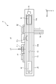
- FIG. 1 is a schematic diagram of the surface treatment apparatus of the first embodiment.
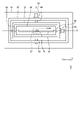
- FIG. 2 is a top view of the interior of the chamber of the surface treatment apparatus of the first embodiment.
- FIG. 3 is an exploded perspective view showing a mounting structure for the material to be treated.
- FIG. 4 is a cross-sectional view showing a mounting structure for the material to be treated.
- FIG. 5 is a front view for explaining a mechanism for adjusting the orientation of the material to be treated.
- FIG. 6 is a side view illustrating a mechanism for adjusting the orientation of the material to be treated.
- FIG. 7 is a top view for explaining a mechanism for adjusting the orientation of the material to be processed.
- FIG. 8 is a diagram for explaining a method of adjusting the inclination of the material to be processed in the height direction.
- FIG. 9 is a diagram for explaining how the orientation of the material to be treated is adjusted when the surface treatment is performed.
- FIG. 10 is a cross-sectional view showing an example of the structure of the HCD electrode.
- FIG. 11 is a cross-sectional view showing an example of the structure of the sputtering electrode.
- FIG. 12 is a diagram showing an example of the surface treatment applied to the material to be treated by the surface treatment apparatus.
- FIG. 13 is a diagram showing an example of pressure changes in the chamber when the surface treatment apparatus applies the surface treatment to the material to be treated.
- FIG. 14 is a flow chart showing an example of the flow of processing performed when the surface treatment apparatus applies the surface treatment to the material to be treated.
- FIG. 15 is an exploded perspective view showing a mounting structure for the material to be treated.
- FIG. 16 is a cross-sectional view showing an example of a state in which a material to be treated is sandwiched between a base and a substrate holder.
- FIG. 17 is a diagram explaining in more detail the method of adjusting the inclination of the material to be processed in the height direction.
- FIG. 18 is a flow chart showing an example of the flow of processing for adjusting the inclination of the material to be processed in the height direction.
- FIG. 19 is a top view of the interior of the chamber of the surface treatment apparatus of the second embodiment.
- FIG. 20 is an exploded perspective view showing the mounting structure of the material to be treated in the surface treatment apparatus of the second embodiment.
- FIG. 21 is a cross-sectional view showing the mounting structure of the material to be treated in the surface treatment apparatus of the second embodiment.
- the first embodiment of the present disclosure is an example of a surface treatment apparatus 10 that performs surface treatment on the surface of a workpiece W (work) having a large area of about 500 x 600 mm, which is molded from a resin material such as plastic resin. is. More specifically, the surface treatment apparatus 10 forms an Al layer, which is a thin film of aluminum (Al), on the surface of the material W to be treated by sputtering. After that, the surface treatment apparatus 10 forms a SiOx film on the surface of the workpiece W by irradiating the Al layer with plasma. The surface of the workpiece W on which the SiOx film is formed has improved environmental resistance. In addition, the surface of the material to be treated W is irradiated with oxygen plasma by the surface treatment apparatus 10 to form a plating seed layer, such as copper, by sputtering. improve sexuality.
- a plating seed layer such as copper
- FIG. 1 is a schematic diagram of the surface treatment apparatus of the first embodiment.
- the surface treatment apparatus 10 includes a chamber 20, which includes a workpiece placement section 50, a workpiece transfer section 40, an HCD (Hollow Cathode Discharge) electrode 21a, and a sputtering electrode 22a. and
- a chamber 20 which includes a workpiece placement section 50, a workpiece transfer section 40, an HCD (Hollow Cathode Discharge) electrode 21a, and a sputtering electrode 22a. and
- the chamber 20 is a closed reaction vessel that performs surface treatment on the material W to be treated that is housed inside.
- the chamber 20 has a rectangular parallelepiped shape whose longitudinal direction is the X-axis direction in the XYZ coordinate system shown in FIG. Note that the chamber 20 is an example of a housing unit in the present disclosure.
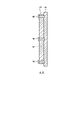
- the processed material placement unit 50 places the processed material W in a state of being substantially erected along the Y-axis direction. It should be noted that the processed material placing section 50 is an example of the placing means in the present disclosure.
- the processed material placement section 50 includes a moving table 41 , a mounting table 47 and a mounting shaft 48 .
- the moving table 41 is a pedestal on which the material W to be treated is installed.
- the moving table 41 is conveyed along the X-axis by a processing material conveying unit 40, which will be described later.
- the moving table 41 is an example of a base member in the present disclosure.
- the mounting base 47 is a member that is installed on the moving base 41 and serves as a base for mounting the material W to be processed. Note that the mount 47 is an example of a base member in the present disclosure.
- the mounting shaft 48 supports the material W to be processed on the mounting base 47 .
- the mounting shaft 48 is an example of a support member in the present disclosure.
- the processed material conveying section 40 conveys the processed material W placed on the processed material placement section 50 along the longitudinal direction (X-axis) of the chamber 20 .
- the processed material conveying unit 40 is an example of conveying means in the present disclosure.
- the processed material conveying unit 40 is a one-axis moving table driven by a conveying motor 43 . Specifically, the material-to-be-processed conveying unit 40 moves the material-to-be-processed placing unit 50 installed on the moving table 41 along the groove 42 .
- the moving table 41 is an example of a base member in the present disclosure.
- the structure of the processed material conveying unit 40 is not limited to the example described in FIG. For example, it may be of a belt conveyor type.
- the sputtering electrode 22a is an electrode of the sputtering device 22, which is an example of the surface treatment means in the present disclosure.
- the sputtering device 22 sputters atoms used for film formation from a target placed on the sputtering electrode 22a and adheres the ejected atoms to the surface of the material W to be processed.
- a thin film which serves as a base for plating, is formed on the surface of the material to be processed W, for example.
- the width (length in the X-axis direction) of the sputtering electrode 22a is shorter than the width (length in the X-axis direction) of the material W to be processed.
- the sputtering electrode 22a is an example of an electrode in the present disclosure.
- the HCD electrode 21a is an electrode of the plasma generator 21, which is an example of the surface treatment means in the present disclosure.
- the plasma generator 21 irradiates the workpiece W on which the thin film is formed by the sputtering device 22 with the plasma generated by the HCD electrode 21a, thereby performing the surface treatment of the workpiece W. , for example a SiO 2 layer.
- the environmental resistance of the surface of the material W to be treated is improved.
- by irradiating the surface of the material W to be treated with oxygen plasma generated by the HCD electrode 21a to form a plating seed layer, for example copper by sputtering, adhesion of the thin film that becomes the base during the plating process in the subsequent process is achieved. improve sexuality.
- the width (length in the X-axis direction) of the HCD electrode 21a is shorter than the width (length in the X-axis direction) of the workpiece W to be processed.
- the HCD electrode 21a is an example of an electrode in the present disclosure.
- the HCD electrode 21a and the sputtering electrode 22a may be divided into a plurality of regions along the Y-axis and each divided region may be controlled with a different output. By adopting such a configuration, it is possible to more uniformly surface-treat a large area of the workpiece W to be treated.
- the processed material placing section 50 includes a first adjusting means for adjusting the orientation of the processed material W. As shown in FIG. More specifically, when the surface treatment is performed, the first adjusting means adjusts the orientation of the material to be treated W around the axis B shown in FIG. Adjustment is made around an axis perpendicular to both the normal direction of the sputtering electrode 22a that constitutes the sputtering device 22 and the normal direction of the HCD electrode 21a that constitutes the plasma generation device 21 . More specifically, the first adjusting means rotates the material W to be processed around the axis B by an amount corresponding to the position of the material W to be processed in the X-axis direction, thereby controlling the spattering of the material W to be processed.
- the position of the axis B is not limited to the position shown in FIG. 1, and may be set at any position parallel to the Y-axis. Adjustments about axis B will be described in detail later (see FIGS. 5-7 and 9).
- the first adjustment means adjusts the orientation of the material W to be treated around the axis C shown in FIG. Thereby, a uniform film can be formed on the surface of the workpiece W having a large area.
- the position of the axis C is not limited to the position shown in FIG. 1, and may be set at any position parallel to the Z axis. Details of the adjustment about the axis C will be described later (see FIGS. 5 to 7).
- the processing material placement unit 50 adjusts the orientation of the processing material W around the axis ⁇ shown in FIG.
- a second adjusting means for adjusting to a predetermined value is provided. This makes it possible to prevent uneven film formation due to the strain when the material W to be processed has strain.
- the position of the axis ⁇ is not limited to the position shown in FIG. 1, and may be set at any position parallel to the X-axis. Details of the adjustment around the axis ⁇ will be described later (see FIGS. 5 to 8).
- the surface treatment apparatus 10 further includes an exhaust device, a cooling device, a control device, a power supply device, a gas supply device, a control panel, etc., but illustration thereof is omitted for the sake of simplicity of explanation.
- the exhaust device reduces the pressure inside the chamber 20 to a vacuum state.
- the evacuation device is composed of, for example, a rotary pump or a turbomolecular pump.
- the cooling system generates cooling water that cools equipment and power supplies.
- the control device controls the surface treatment apparatus 10 as a whole.
- the power supply device accommodates power to be supplied to each part of the surface treatment apparatus 10 .
- the gas supply device supplies film-forming gas and reaction gas to the chamber 20 .
- the operation panel accepts operation instructions for the surface treatment apparatus 10.
- the operation panel also has a function of displaying the operating state of the surface treatment apparatus 10 .
- the surface treatment apparatus 10 performs the plasma treatment on the material W to be treated. You may perform a sputtering process by . Further, in the present embodiment, the surface treatment apparatus 10 is assumed to have two types of surface treatment means, the sputtering apparatus 22 and the plasma generation apparatus 21, but at least one type of surface treatment means may be provided.
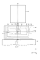
- FIG. 2 is a top view of the interior of the chamber of the surface treatment apparatus of the first embodiment.
- the chamber 20 includes a shutter 30, a shutter 31, and a shutter 32.
- the shutter 30 partitions the interior of the chamber 20 into a load lock chamber 20a and a reaction chamber 20b by moving in the negative direction of the Z axis. After the shutter 30 is closed and the material W to be processed is placed in the load lock chamber 20a, the pressure inside the load lock chamber 20a is reduced to remove atmospheric components adhering to the material W to be processed. After that, the shutter 30 is opened, and the material W to be treated is conveyed to the reaction chamber 20b for surface treatment (film formation treatment).
- the shutters 30, 31 and 32 may be opened and closed by providing standby positions for the shutters 30, 31 and 32 above the chamber 20 and moving the shutters 30, 31 and 32 along the Y-axis.
- the shutter 31 exposes the HCD electrode 21a when plasma processing is performed on the workpiece W by moving in the positive direction of the X axis. Further, the shutter 31 retracts the HCD electrode 21a when the material W to be processed is subjected to the sputtering process by moving in the negative direction of the X-axis. This prevents contamination of unused electrodes. Note that the shutter 31 is an example of a shielding member in the present disclosure.
- the shutter 32 exposes the sputtering electrode 22a when sputtering the material W to be processed by moving in the negative direction of the X axis. Further, the shutter 32 retracts the sputtering electrode 22a when performing the plasma processing on the workpiece W by moving in the positive direction of the X-axis. This prevents contamination of unused electrodes. Note that the shutter 32 is an example of a shielding member in the present disclosure.
- the HCD electrode 21a is movable along an axis Z1 parallel to the Z axis. Thus, by setting the distance between the workpiece W and the HCD electrode 210a to an optimum value, a more uniform film formation process can be performed.
- the sputtering electrode 22a is movable along an axis Z2 parallel to the Z axis. Thus, by setting the distance between the material to be processed W and the sputtering electrode 22a to an optimum value, a more uniform film forming process can be performed.
- the degree of vacuum in the chamber 20 may be appropriately changed according to values such as the value, current value, discharge state, temperature inside the chamber 20, and the like. This enables a more uniform film formation process. Further, the conveying speed of the material to be treated W may be changed according to the value of each parameter described above.
- the workpiece W that has undergone the sputtering process and the plasma process moves to the position indicated by the dotted line shown in FIG. After that, the material W to be processed is moved to the position of the load lock chamber 20a. Then, after the shutter 30 is closed and the pressure inside the load lock chamber 20 a is increased to the atmospheric pressure, the workpiece W on which the film forming process is completed is taken out from the chamber 20 .
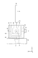
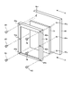
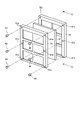
- FIG. 3 is an exploded perspective view showing a mounting structure for the material to be treated.
- FIG. 4 is a cross-sectional view showing a mounting structure for the material to be treated.
- the material to be treated W is attached to the material to be treated mounting portion 50 while being sandwiched between the base 44 and the substrate holder 45 .
- the base 44 is a plate-shaped member that is one size larger than the material W to be processed and holds the surface of the material W to be processed that is not subjected to surface treatment in contact with it.
- the substrate holder 45 is a plate-like member formed in a grid.
- the substrate holder 45 has a thickness greater than the thickness of the material W to be treated, as shown in FIG.
- the back side of the substrate holder 45 (the side that abuts on the material W to be treated) is formed to have a small thickness in accordance with the shape of the material W to be treated.
- a substrate holder 45 having only an outer frame without a grid may be used. Since residual stress may be generated in W, it is desirable to use a substrate holder 45 having a lattice to fix the workpiece W while firmly pressing it against the base 44 .
- a plurality of mounting holes 45 a through which screws 46 pass are formed in the outer edge of the substrate holder 45 .
- the screw 46 inserted into the mounting hole 45a is coupled with a female screw 44a formed in the base 44, thereby fixing the substrate holder 45 and the base 44 while holding the material W to be processed. do.
- the substrate holder 45 and the base 44 may be fixed using a one-touch clip or the like instead of the screws 46 .
- FIG. 5 is a front view for explaining a mechanism for adjusting the orientation of the material to be treated.
- FIG. 6 is a side view illustrating a mechanism for adjusting the orientation of the material to be treated.
- FIG. 7 is a top view for explaining a mechanism for adjusting the orientation of the material to be processed. 5, 6, and 7 are drawn with the base 44 and the substrate holder 45 omitted for the sake of simplicity of explanation.
- a C-axis turntable 51 and a ⁇ -axis turntable 52 are installed inside the mounting base 47 .
- the C-axis rotating base 51 is attached to the mounting base 47 by a mounting shaft 56 so as to be rotatable about the axis C with respect to the mounting base 47 .
- the C-axis turntable 51 rotates (swings) around the axis C by the rotational driving force of the C-axis rotary motor 55 .
- the C-axis rotary motor 55 is, for example, a step motor, a servo motor, or the like, which can instruct the rotation angle from the outside.
- the C-axis rotary motor 55 is a motor that can be used in a vacuum environment. It should be noted that the C-axis rotary motor 55 is an example of the first adjusting means in the present disclosure.
- the ⁇ -axis turntable 52 is attached to the C-axis turntable 51 by a mounting shaft 54 so as to be rotatable about the axis ⁇ with respect to the mount 47 .
- the ⁇ -axis turntable 52 is rotated around the ⁇ -axis by the rotational driving force of the ⁇ -axis rotating motor 53 .
- the ⁇ -axis rotating motor 53 is, for example, a step motor, a servo motor, or the like, which can instruct the rotation angle from the outside.
- the ⁇ -axis rotating motor 53 is a motor that can be used in a vacuum environment.
- the ⁇ -axis rotating motor 53 is an example of the second adjustment means in the present disclosure.
- the mounting base 47 is mounted on the moving base 41 by a mounting shaft 58 so as to be rotatable about the axis B with respect to the moving base 41 .
- the mounting base 47 rotates around the axis B by the rotational driving force of the B-axis rotating motor 57 .
- the mounting table 47 is a B-axis rotating table.
- the B-axis rotary motor 57 is, for example, a step motor, a servo motor, or the like, which can instruct the rotation angle from the outside.
- the B-axis rotating motor 57 is a motor that can be used in a vacuum environment. It should be noted that the B-axis rotating motor 57 is an example of the first adjustment means in the present disclosure.
- the configurations of the axis B, the axis C, the rotation mechanism around the axis ⁇ , and the transport mechanism in the X-axis direction are not limited to the examples shown in FIGS. 1 and 5 to 7.
- FIG. it is possible to rotate the workpiece W around the axis C without using a motor. That is, the translational motion of the moving table 41 in the X-axis direction may be converted into the rotational motion of the pinion gear by the rack and pinion mechanism, and the rotational motion may be transmitted to the workpiece W through the floating joint.
- the material W to be treated can be rotated around the axis C without using a motor.
- the number of revolutions of the workpiece W around the axis C is determined by the gear ratio of the rack and pinion and the transport speed in the X-axis direction.
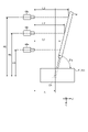
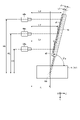
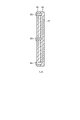
- FIG. 8 is a diagram illustrating a method of adjusting the inclination of the material to be treated in the height direction (inclination with respect to the Y-axis).
- the surface treatment apparatus 10 includes laser length measuring devices 60a, 60b, and 60c inside the load lock chamber 20a.
- the laser length measuring instruments 60a, 60b, 60c are installed at different height positions along the Y-axis. That is, the laser length measuring devices 60a, 60b, and 60c are installed at heights H1, H2, and H3 from a reference position (for example, the position of the mounting shaft 54).
- the Z-axis direction positions of the laser length measuring devices 60a, 60b, and 60c are the same.
- Laser length measuring instruments 60a, 60b, and 60c when laser light of a predetermined wavelength is emitted, determine the phase of the emitted laser light and the amount of light reflected by the surface of the object and returning to the laser length measuring instruments 60a, 60b, and 60c. It measures the phase shift of the laser light. Based on the measured phase shift, distances L1m, L2m, and L3m to the surface of the workpiece W stored in the load lock chamber 20a are measured.
- FIG. 8 shows a state in which the material W to be processed is placed with an inclination with respect to the Y-axis in a non-distorted state. More specifically, the material W to be treated is placed at an angle (90- ⁇ a) with respect to the Y-axis.
- the theoretical distances L1, L2, and L3 measured by the laser length measuring devices 60a, 60b, and 60c are calculated by equations (1), (2), and (3), respectively.
- A is the mounting shaft 54 (Fig. 5 to FIG. 7).
- the surface treatment apparatus 10 has a function of changing the inclination of the material W to be treated with respect to the Y-axis. Specifically, the surface treatment apparatus 10 minimizes the sum of the difference values between the distances L1m, L2m, L3m actually measured by the laser length measuring devices 60a, 60b, 60c and the theoretical distances L1, L2, L3. The inclination (that is, the angle (90- ⁇ a)) of the workpiece W with respect to the Y-axis is changed so that
- the number of locations where the distance is measured is not limited to three, and the distance may be measured at more height positions.
- FIG. 9 is a diagram for explaining how the orientation of the material to be treated is adjusted when the surface treatment is performed.
- the surface treatment apparatus 10 oscillates the workpiece W around the axis B by controlling the rotation of the B-axis rotary motor 57 during sputtering. This swinging adjusts the orientation (normal direction) of the material W to be treated to the orientation corresponding to the position in the X-axis direction. More specifically, as shown in FIG. 9, the normal direction of the workpiece W is adjusted to face the direction of the sputtering electrode 22a.
- the B-axis rotating motor 57 directs the normal direction of the material to be processed W to the direction of the sputtering electrode 22a. adjust to
- the B-axis rotary motor 57 adjusts the normal direction of the material to be processed W to face the direction of the sputtering electrode 22a.
- the B-axis rotary motor 57 adjusts the normal direction of the material W to be processed so as to face the direction of the sputtering electrode 22a.
- the B-axis rotary motor 57 controls the rotation of the B-axis rotary motor 57 based on the position of the material W to be processed in the X-axis direction and the position of the sputtering electrode 22a.
- the surface treatment apparatus 10 After the sputtering of the material W to be processed by the sputtering electrode 22a is completed, the surface treatment apparatus 10 once moves the material W to be processed in the negative direction of the X axis (rightward in FIG. 9). Then, plasma processing is performed by the HCD electrode 21a. Also when plasma processing is performed, the B-axis rotating motor 57 adjusts the normal direction of the workpiece W to face the direction of the sputtering electrode 22a.
- the surface treatment apparatus 10 controls the rotation of the C-axis rotary motor 55 while performing the sputtering and plasma processing on the material W to be processed. Oscillate W about axis C; Due to this rocking motion, the surface of the material W to be treated is treated more uniformly.
- the specific rocking pattern around the axis B and the specific rocking pattern around the axis C depend on the material W to be treated, the electrode to be used, the details of the surface treatment, the conditions of the surface treatment, and the like. determined accordingly.
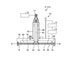
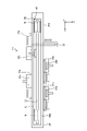
- FIG. 10 is a cross-sectional view showing an example of the structure of the HCD electrode.
- the HCD electrode 21a constituting the plasma generation device 21 includes a gas supply pipe 68 for supplying a gas such as argon, which is used for generating plasma, and a high-frequency voltage to generate plasma from the gas supplied from the gas supply pipe 68. It has a pair of plate-like conductor portions 64 and 66 that are connected to each other.
- a gas flow path 61 is formed along the extending direction of the gas supply pipe 68, and gas is supplied from the outside of the chamber 20 into the chamber 20 through the gas flow path 61. do.
- a gas supply unit 77 for supplying gas to the gas supply pipe 68 is connected to the end of the gas supply pipe 68 outside the chamber 20 , and the end of the gas supply pipe 68 inside the chamber 20 is connected to the gas supply unit 77 .
- Gas is supplied to the gas supply unit 77 via a mass flow controller (MFC) 75 which is a mass flow meter provided with a flow rate control function.
- MFC mass flow controller
- the pair of plate-shaped conductor portions 64 and 66 are both formed in a flat plate shape, and are formed by arranging metal plates such as aluminum or other conductor plates in parallel.
- the plate-shaped conductor portions 64 and 66 are supported by a support plate 76 .
- the support plate 76 is made of, for example, an insulating material such as glass or ceramic.
- the support plate 76 is formed in a shape in which a convex portion is formed over the entire circumference near the outer periphery on one side of the plate. In other words, the support plate 76 is formed in a plate-like shape with a concave portion 69 formed along the outer periphery of the support plate 76 on one side.
- the surface of the support plate 76 on which the recess 69 is not formed is supported by a cylindrical support member 63 that surrounds the gas supply pipe 68 along the extending direction.
- the gas supply pipe 68 extends through the inside of the cylindrical member of the support member 63 to the position of the support plate 76 and penetrates the support plate 76 .
- the gas supply hole 62 formed in the gas supply pipe 68 is arranged in the portion of the support plate 76 where the concave portion 69 is formed.
- the pair of plate-shaped conductors 64 and 66 are arranged on the side of the support plate 76 where the recess 69 is formed, covering the recess 69 . At that time, the pair of plate-like conductor portions 64 and 66 are overlapped with a spacer 67 disposed near the outer periphery between the two with the spacer 67 therebetween. In the pair of plate-shaped conductors 64 and 66 that are stacked with the spacer 67 interposed therebetween, the plate-shaped conductor 64 and the plate-shaped conductor 66 are separated from each other in a portion other than the spacer 67 to form a gap 65. ing.
- the interval of the gap 65 is preferably set appropriately according to the gas to be introduced into the plasma generator 21, the frequency of the power to be supplied, the size of the electrode, etc., and is, for example, about 3 mm to 12 mm.
- the pair of plate-shaped conductors 64 and 66 are held by a holding member 78 which is a member for holding the plate-shaped conductors 64 and 66 in a state of being superimposed via a spacer 67 . That is, the holding member 78 is arranged on the opposite side of the plate-shaped conductors 64 and 66 to the side where the support plate 76 is located, and the holding member 78 and the support plate 76 support the plate-shaped conductors 64 and 66 while sandwiching them. It is attached to plate 76 .
- the pair of plate-shaped conductors 64 and 66 are arranged so as to cover the recess 69 in the support plate 76 in this manner. A space is formed between 64 and 66 .
- the space is defined by the recessed portion 69 of the support plate 76 and the plate-shaped conductor portion 66 .
- the space formed in this manner is formed as a gas introduction portion 79 into which the gas supplied by the gas supply pipe 68 is introduced.
- the gas supply hole 62 of the gas supply pipe 68 is located in the gas introduction portion 79 and opens toward the gas introduction portion 79 .
- the gas introduction portion 79 is defined by attaching the support plate 76 and the plate-like conductor portion 66 in close contact with each other.
- a large number of through holes 70 and 71 penetrating in the thickness direction are formed in the pair of plate-shaped conductor portions 64 and 66, respectively. That is, the plate-like conductor portion 66 located on the inflow side of the gas supplied from the gas supply pipe 68 has a plurality of through holes arranged in a matrix at predetermined intervals when viewed in the thickness direction of the plate-like conductor portion 66 . 71 are formed in the plate-like conductor portion 64 located on the outflow side of the gas supplied by the gas supply pipe 68, and are arranged in a matrix at predetermined intervals when viewed in the thickness direction of the plate-like conductor portion 64. , a plurality of through holes 70 are formed.
- the through-hole 70 of the plate-shaped conductor portion 64 and the through-hole 71 of the plate-shaped conductor portion 66 are cylindrical holes, respectively, and both the through-holes 70 and 71 are coaxially arranged. That is, the through hole 70 of the plate-shaped conductor portion 64 and the through hole 71 of the plate-shaped conductor portion 66 are arranged at positions where the centers of the respective through holes are aligned. Among them, the through-hole 70 of the plate-shaped conductor portion 64 has a smaller diameter than the through-hole 71 of the plate-shaped conductor portion 66 on the gas inflow side. In this manner, a plurality of through holes 70 and 71 are formed in the pair of plate-shaped conductor portions 64 and 66 to form a hollow electrode structure. flow in density.
- a space 65 is interposed between the parallel-plate plate-shaped conductors 64 and 66, and the space 65 functions as a capacitor having capacitance.
- Conductive portions (not shown) are formed on the support plate 76 and the plate-shaped conductor portions 64 and 66 by a conductive member, and the support plate 76 is grounded 74 by the conductive portions. It is grounded 74 .
- One end of the high-frequency power supply (RF) 73 is grounded 74, and the other end of the high-frequency power supply 73 is connected to a matching box (MB ) 72 to the plate-like conductor portion 64 . Therefore, when the high-frequency power supply 73 is operated, the potential of the plate-shaped conductor portion 64 swings between positive and negative at a predetermined frequency such as 13.56 MHz.
- the plasma gas flowing out from the through-holes 70 performs surface treatment such as film formation and cleaning of the workpiece W in the chamber 20 .
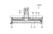
- FIG. 11 is a cross-sectional view showing an example of the structure of the sputtering electrode.
- the sputtering device 22 includes a cooling water pipe 81 through which cooling water flows, a magnet 84 that generates a magnetic field, and a gas supply unit (not shown) that supplies gas inside the magnetic field generated by the magnet 84 to a gas inlet (not shown).
- a target 87 that ejects atoms used for film formation by ionizing and colliding with an inert gas (for example, argon) flowed in from the target 87, a cooling jacket 85 that cools the target 87, a magnet 84, the target 87, and the cooling jacket 85. and a support plate 83 for supporting the
- the cooling water pipe 81 penetrates through the support plate 83 .
- the target 87 is, for example, an aluminum plate, and aluminum atoms ejected from the target 87 adhere to the surface of the material W to be processed, thereby forming a thin aluminum film on the surface of the material W to be processed.
- a cooling water passage 82 is formed inside the cooling water pipe 81 along the extending direction of the cooling water pipe 81 .
- the cooling water passage 82 includes a water passage for supplying cooling water from the outside of the chamber 20 to the cooling jacket 85 for cooling, and a water passage for supplying cooling water from the cooling jacket 85 to the outside of the chamber 20 for cooling. and a water channel for discharging the cooled water.
- the cooling water pipes 81 circulate cooling water between the outside of the chamber 20 and the cooling jacket 85 located within the chamber 20 .
- An inflow path and a discharge path for cooling water not shown in FIG.
- the other end of the cooling water pipe 81 (inside the chamber 20 ) is connected to a cooling jacket 85 .
- the cooling jacket 85 has a cooling water flow path formed therein, through which the cooling water flows. Thereby, cooling water circulates between the outside of the chamber 20 and the cooling jacket 85 . Cooling water is supplied from a cooling device (not shown).
- the support plate 83 supports the magnet 84, the cooling jacket 85, and the target 87 in an overlapping state.
- the support plate 83, the magnet 84, the cooling jacket 85, and the target 87 are all plate-shaped, and the support plate 83 is flatter than the magnet 84, the cooling jacket 85, and the target 87. It is formed in a shape with a large visual shape. Therefore, the magnet 84, the cooling jacket 85, and the target 87 are stacked in the order of the magnet 84, the cooling jacket 85, and the target 87 from the support plate 83 side. It is held by the support plate 83 and the holding member 88 by supporting the periphery of the side surface by the holding member 88 .
- the magnet 84 , the cooling jacket 85 , and the target 87 held by the holding member 88 are also held in such a manner that their outer peripheral portions are also surrounded by the holding member 88 .
- an insulating material 86 is arranged between the support plate 83 and the magnet 84, and the insulating material 86 is also arranged on the outer peripheral portion of the magnet 84 in plan view. That is, the insulating material 86 is arranged between the support plate 83 and the magnet 84 and between the magnet 84 and the holding member 88 . Therefore, the magnet 84 is held by the support plate 83 and the holding member 88 via the insulating material 86 .
- the sputtering device 22 performs so-called sputtering for forming a thin film on the surface of the material W to be processed.
- the pressure inside the chamber 20 is reduced by an exhaust device (not shown), and then a gas used for sputtering is introduced into the chamber 20 from a gas supply device (not shown).
- the gas in the chamber 20 is ionized by the magnetic field generated by the magnet 84 of the sputtering device 22 , and the ions collide with the target 87 . This ejects the atoms of the target 87 from the surface of the target 87 .
- the target 87 ejects aluminum atoms when gas ions ionized in the vicinity of the target 87 collide with the target 87.
- Aluminum atoms ejected from the target 87 are directed in the positive direction of the Z-axis. Since the material W to be processed is located at a position facing the surface of the target 87 in the chamber 20, the aluminum atoms ejected from the target 87 move toward the material W to be processed and adhere to the material W to be processed. and deposited on the surface of the material W to be treated. As a result, a thin film corresponding to the material forming the target 87 is formed on the surface of the material W to be processed.
- FIG. 12 is a diagram showing an example of the surface treatment applied to the material to be treated by the surface treatment apparatus.
- FIG. 13 is a diagram showing an example of pressure changes in the chamber when the surface treatment apparatus applies the surface treatment to the material to be treated.
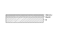
- the surface treatment apparatus 10 forms an Al layer 90a and a SiO 2 layer 90b on one side of the material W to be treated, for example.
- the surface treatment apparatus 10 operates the sputtering apparatus 22 to form an Al layer 90a, which is a thin film of aluminum (Al), on the surface of the workpiece W to be treated.
- the inside of the chamber 20 is reduced to a pressure P0 (for example, from 10 ⁇ 2 to 10 ⁇ 3 Pa) at time t0 by introducing a gas into the chamber 20 from a pressure P0 (for example, 10 ⁇ 2 to 10 ⁇ 3 Pa).
- Aluminum is sputtered under a pressure of .
- the pressure P1 is 20 Pa, for example.
- the pressure inside the chamber 20 is again reduced to the pressure P0 at time t1.
- the vertical axis indicates the pressure P, and indicates a state in which the pressure is decreased toward the bottom.
- the surface treatment apparatus 10 oscillates the workpiece W around the axis B and around the axis C while the sputtering is being performed. As a result, a uniform Al layer 90a is formed on the surface of the material W to be processed.
- the surface treatment apparatus 10 generates the SiO 2 layer 90b on the surface of the Al layer 90a of the workpiece W to be treated by operating the plasma generation apparatus 21 .
- the surface treatment apparatus 10 pressurizes the inside of the chamber 20 from the pressure P0 at time t1 to the pressure P2 by introducing the gas.
- the plasma generator 21 generates a SiO 2 layer 90b (polymer film) on the surface of the Al layer 90a of the material W to be processed.
- the pressure P2 is set to a pressure higher than the pressure P1.
- the pressure P2 is 30 Pa, for example.
- the surface treatment apparatus 10 swings the workpiece W around the axis B and around the axis C while the plasma treatment is being performed. Thereby, a uniform SiO 2 layer 90b is formed on the surface of the material W to be processed.
- the surface treatment apparatus 10 moves the material W to be treated to the load lock chamber 20a. Then, the surface treatment apparatus 10 closes the shutter 30 and increases the pressure inside the load lock chamber 20a to the atmospheric pressure. After that, the material to be processed W on which the film forming process has been completed is taken out from the chamber 20 .
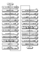
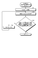
- FIG. 14 is a flow chart showing an example of the flow of processing performed when the surface treatment apparatus applies the surface treatment to the material to be treated.
- the surface treatment apparatus 10 closes the shutter 30 of the load lock chamber 20a (step S11).
- the operator of the surface treatment apparatus 10 places the material W to be treated in the load lock chamber 20a (step S12).
- the surface treatment apparatus 10 measures distances L1m, L2m, and L3m to the surface of the material W to be treated by laser length measuring devices 60a, 60b, and 60c. Then, the rotation angle of the workpiece W around the ⁇ axis is adjusted so that the errors between the measured distances L1m, L2m, L3m and the theoretical distances L1, L2, L3 are minimized (step S13).
- the surface treatment apparatus 10 reduces the pressure in the load lock chamber 20a (step S14).
- the surface treatment apparatus 10 opens the shutter 32 for the sputtering electrode 22a (step S15).
- the surface treatment apparatus 10 closes the shutter 31 for the HCD electrode 21a (step S16).
- the surface treatment apparatus 10 reduces the pressure inside the reaction chamber 20b of the chamber 20 to the pressure P0 (step S17).
- the surface treatment apparatus 10 opens the shutter 30 of the load lock chamber 20a (step S18).
- the surface treatment apparatus 10 pressurizes the inside of the reaction chamber 20b of the chamber 20 to the pressure P1 (step S19).
- the surface treatment apparatus 10 starts moving the material W to be treated in the X-axis direction (step S20).
- the surface treatment apparatus 10 swings the material W to be treated around the B-axis and the C-axis according to the position in the X-axis direction (step S21).
- the sputtering device 22 forms an Al film on the surface of the workpiece W (step S22).
- the surface treatment apparatus 10 moves the material W to be treated to the plasma treatment start position (step S23).
- the surface treatment apparatus 10 reduces the pressure inside the reaction chamber 20b of the chamber 20 to the pressure P0 (step S24).
- the surface treatment apparatus 10 closes the shutter 32 for the sputtering electrode 22a (step S25).
- the surface treatment apparatus 10 opens the shutter 31 for the HCD electrode 21a (step S26).
- the surface treatment apparatus 10 pressurizes the inside of the reaction chamber 20b of the chamber 20 to the pressure P2 (step S27).
- the surface treatment apparatus 10 starts moving the material W to be treated in the X-axis direction (step S28).
- the surface treatment apparatus 10 swings the material W to be treated around the B-axis and the C-axis according to the position in the X-axis direction (step S29).
- the plasma generator 21 forms a SiO 2 film on the surface of the material W to be processed (step S30).
- the surface treatment apparatus 10 moves the material W to be treated to the load lock chamber 20a (step S31).
- the surface treatment apparatus 10 closes the shutter 30 of the load lock chamber 20a (step S32).
- the surface treatment apparatus 10 opens the load lock chamber 20a to the atmosphere (step S33).
- the operator of the surface treatment apparatus 10 takes out the workpiece W for which the surface treatment has been completed from the load lock chamber 20a (step S34).
- the series of processes described above may be executed based on an operator's instruction, or may be executed automatically according to a pre-created sequence.
- the surface treatment apparatus 10 of the first embodiment includes the workpiece placing portion 50 (placing means) on which the workpiece W is placed, and the workpiece placed on the workpiece placing portion 50.
- a chamber 20 accommodated the treated material W
- a plasma generator 21 and a sputtering apparatus 22 surface treatment means for performing at least one type of surface treatment on the treated material W accommodated in the chamber 20.
- a processing material conveying unit 40 (conveying means) that conveys the processing material W placed on the processing material mounting unit 50 along the plasma generation device 21 and the sputtering device 22, and the direction of the processing material W are adjusted according to the transport position of the material transporting unit 40 and the position of the plasma generating device 21 or the sputtering device 22 . Therefore, it is possible to provide a surface treatment apparatus suitable for surface treatment of a small to medium amount of material W to be treated. In addition, since the surface treatment apparatus 10 performs film formation while moving the material W to be treated, the width of the electrode can be narrowed, and the output per unit area of the electrode can be increased accordingly.
- the film forming process can be performed even under a low vacuum, so that the evacuation time can be shortened. Furthermore, since the vacuum is low, the amount of outgassing generated in the chamber 20 during the film formation process is reduced, which leads to shortening of the evacuation time and exhaust time, and shortens the manufacturing takt time. can be done. Moreover, when the output per unit area of the electrode is the same as that of the conventional electrode, the power output of the electrode can be reduced, and the cost performance of the device can be improved.
- the B-axis rotating motor 57 (first adjusting means) adjusts the orientation of the material to be treated W to the direction of conveyance of the material to be treated conveying section 40 (conveying means).
- the B-axis rotating motor 57 adjusts the orientation of the material to be treated W to the direction of conveyance of the material to be treated conveying section 40 (conveying means).
- the C-axis rotating motor 55 (first adjusting means) adjusts the orientation of the material W to be treated around the normal direction of the material W to be treated. . Therefore, the surface of the material W to be treated can be uniformly surface-treated.
- the surface treatment apparatus 10 of the first embodiment includes a laser measuring device for measuring strain in the height direction of the workpiece W before the plasma generation device 21 or the sputtering device 22 (surface treatment means) performs surface treatment. Based on the distortion of the workpiece W measured by the length instruments 60a, 60b, 60c (measuring means) and the laser length measuring instruments 60a, 60b, 60c, the inclination of the workpiece W in the height direction is set to a predetermined value. and a ⁇ -axis rotating motor 53 (second adjusting means) for adjustment. Therefore, the strain state of the material W to be surface-treated can be accurately measured.
- the laser length measuring devices 60a, 60b, and 60c are laser length measuring devices measured at a plurality of different positions in the height direction of the material W to be treated. Based on the distances L1m, L2m, L3m between the vessels 60a, 60b, 60c and the material W to be processed, the strain in the height direction of the material W to be processed is measured. Therefore, it is possible to adjust the attitude of the workpiece W so that the influence of distortion during surface treatment is minimized.
- the treatment material placing section 50 is a moving table 41 (pedestal member) conveyed by the treatment material conveying section 40 (conveying means).
- a mounting base 47 base member installed on the moving table 41 to fix the material W to be treated
- a mounting shaft 48 supporting the material W to be treated on the mounting table 47 . Therefore, the orientation of the workpiece W can be adjusted by adjusting the orientation of the mounting table 47 with respect to the moving table 41 and the rotation angle of the mounting shaft 48 with respect to the mounting table 47 .
- the width of the electrodes provided in the plasma generation device 21 and the sputtering device 22 (surface treatment means) along the transfer direction of the material to be treated transfer section 40 (transfer means) is It is smaller than the width of the material W to be processed along the transport direction of the material transport unit 40 to be processed. Therefore, the overall size of the surface treatment apparatus 10 can be kept small.
- the surface treatment apparatus 10 of the first embodiment includes a plasma generator 21 (surface treatment means) that performs surface treatment of the material W to be treated by irradiating the material W to be treated with plasma. Therefore, by forming, for example, a SiO 2 layer on the surface of the material W to be treated, the adhesion of the thin film formed thereafter can be improved.
- a plasma generator 21 surface treatment means
- the surface treatment apparatus 10 of the first embodiment includes a sputtering apparatus 22 (surface treatment means) that performs sputtering on the material W to be treated. Therefore, a desired thin film can be formed on the surface of the material W to be processed.
- a sputtering apparatus 22 surface treatment means
- the surface treatment apparatus 10 of the first embodiment is configured such that when one of the plasma generation apparatus 21 and the sputtering apparatus 22 (surface treatment means) performs surface treatment on the workpiece W, the surface treatment means It further includes shutters 31 and 32 (shielding members) that shield the other surface treatment means. Therefore, it is possible to prevent contamination of the electrodes constituting the surface treatment means that are not related to the surface treatment.
- FIG. 15 is an exploded perspective view showing a mounting structure for the material to be treated.
- FIG. 16 is a cross-sectional view showing an example of a state in which a material to be treated is sandwiched between a base and a substrate holder.
- FIG. 17 is a diagram explaining in more detail the method of adjusting the inclination of the material to be processed in the height direction.
- FIG. 18 is a flow chart showing an example of the flow of processing for adjusting the inclination of the material to be processed in the height direction.
- the surface treatment is performed on the entire surface of the material W to be treated. That is, as shown in FIG. 15, the material W to be treated is held in a state of being sandwiched between the base 44 and the substrate holder 49 . Unlike the substrate holder 45 described above, the substrate holder 49 does not have a grid-shaped pressing member. Therefore, the surface treatment can be performed over the entire surface of the material W to be treated.
- the base 44 and the substrate holder 49 are screwed together with screws 46 . More specifically, screws 46 inserted through a plurality of mounting holes 49a formed in the outer edge of substrate holder 49 are coupled to female threads 44a formed in base 44, thereby connecting base 44 and base 44 together.
- the material holder 49 is coupled with the material W to be processed sandwiched therebetween.
- the material W to be processed is gripped only by the outer frame of the substrate holder 49, so that the material W to be processed may bend due to its own weight, as shown in FIG. If surface treatment is performed while the material W to be treated is bent, residual stress may occur in the deposited film itself. This residual stress may cause defects such as cracks and peeling in the material W to be processed.
- FIG. 17 is a more detailed view in which the thickness u1 of the material W to be processed and the half value u2 of the thickness of the base 44 are added to FIG.
- FIG. 17 shows a state in which the material W to be processed is placed with an inclination with respect to the Y-axis in a non-distorted state. More specifically, the material W to be treated is placed at an angle (90- ⁇ a) with respect to the Y-axis.
- the theoretical distances L1, L2, and L3 measured by the laser length measuring devices 60a, 60b, and 60c are calculated by equations (4), (5), and (6), respectively.
- formulas (4), (5), and (6) are added to the above-described formulas (1), (2), and (3), respectively, with the thickness u1 of the workpiece W and the base 44 and the value u2, which is 1/2 of the thickness of 44, is taken into consideration.
- the surface treatment apparatus 10 adjusts the inclination of the material W to be treated with respect to the Y-axis (that is, the angle (90- ⁇ a)) so that the bending of the material W to be treated is less than a predetermined value. Specifically, the surface treatment apparatus 10 allows the difference values between the distances L1m, L2m, and L3m actually measured by the laser length measuring devices 60a, 60b, and 60c and the theoretical distances L1, L2, and L3 to be acceptable.
- the inclination of the workpiece W with respect to the Y-axis that is, the rotation angle about the ⁇ -axis is adjusted so that the deformation amount ⁇ or less.
- the allowable deformation amount ⁇ is obtained in advance by analysis or experiment. Since the location where the material to be treated W is greatly bent can be estimated in advance, only the estimated location may be measured by the laser length measuring device.
- the surface treatment apparatus 10 measures the distance L1m, the distance L2m, and the distance L3m (step S42).
- the surface treatment apparatus 10 calculates the difference between the distance L1m and the theoretical distance L1 obtained by the equation (4), the difference between the distance L2m and the theoretical distance L2 obtained by the equation (5), the distance L3m and the theoretical distance L3 obtained by the equation (6). is equal to or less than the allowable deformation amount ⁇ (step S43).
- the surface processing apparatus 10 ends the adjustment processing of the rotation angle around the ⁇ axis.
- the process proceeds to step S44.
- step S43 if none of the difference values is determined to be equal to or less than the allowable deformation amount ⁇ , the surface treatment apparatus 10 decreases the angle ⁇ a by a predetermined angle ⁇ (step S44). Then, it returns to step S42 and repeats the above-described processing.
- the surface treatment device 11 performs surface treatment on both surfaces of the material W to be treated.
- FIG. 19 is a top view of the interior of the chamber of the surface treatment apparatus of the second embodiment.
- the surface treatment device 11 performs surface treatment on both surfaces of the material W to be treated while conveying the material W to be treated in the X-axis direction.
- the basic structure of the surface treatment apparatus 11 is the same as the structure of the surface treatment apparatus 10 (see FIG. 2).
- electrodes for performing the surface treatment are provided on both sides in the Z-axis direction with the material conveying unit 40 interposed therebetween.
- the HCD electrode 21a and the sputtering electrode 22a are provided on the Z-axis negative side.
- an HCD electrode 21b and a sputtering electrode 22b are provided on the Z-axis positive side.
- the HCD electrode 21a and the sputtering electrode 22a are provided with shutters 31a and 32a for closing or opening each electrode, respectively.
- a shutter 31a and a shutter 32a correspond to the shutter 31 and the shutter 32 described in the first embodiment, respectively.
- the shutters 31a and 32a are examples of shielding members in the present disclosure.
- the HCD electrode 21b and the sputtering electrode 22b are provided with shutters 31b and 32b for closing or opening each electrode, respectively.
- the shutter 31b moves in the positive direction of the X-axis to expose the HCD electrode 21b when plasma processing is performed on the surface of the workpiece W on the positive side of the Z-axis. Also, the shutter 31b retracts the HCD electrode 21b by moving in the negative direction of the X-axis. This prevents contamination of unused electrodes.
- the shutter 31b is an example of a shielding member in the present disclosure.
- the shutter 32b moves in the negative direction of the X-axis to expose the sputtering electrode 22b when sputtering the surface of the workpiece W on the positive side of the Z-axis. Also, the shutter 32b retracts the sputtering electrode 22a by moving in the positive direction of the X-axis. This prevents contamination of unused electrodes. Note that the shutter 32b is an example of a shielding member in the present disclosure.
- the surface treatment apparatus 11 causes the workpiece W to be treated with the same rocking motion when performing the surface treatment with the sputtering electrode 22a and the HCD electrode 21a and when performing the surface treatment with the sputtering electrode 22b and the HCD electrode 21b.
- the surface treatment apparatus 11 is arranged in the direction of the axis .theta. By changing the rotation angle, the attitude of the material W to be treated with respect to each electrode surface is kept constant.
- FIG. 20 is an exploded perspective view showing the mounting structure of the material to be treated in the surface treatment apparatus of the second embodiment.
- FIG. 21 is a cross-sectional view showing the mounting structure of the material to be treated in the surface treatment apparatus of the second embodiment.
- the material to be treated W is attached to the material to be treated mounting portion 50 while being sandwiched between two substrate holders 91 and 92 .
- the substrate holders 91 and 92 are plate-like members formed in a lattice. As shown in FIG. 21, the base material holders 91 and 92 are formed to have a small thickness on the side that abuts on the material W to be processed so as to match the shape of the material W to be processed. Therefore, when the material to be treated W is sandwiched between the substrate holders 91 and 92, the material to be treated W is securely sandwiched between the two substrate holders 91 and 92.
- FIG. 21 The substrate holders 91 and 92 are plate-like members formed in a lattice. As shown in FIG. 21, the base material holders 91 and 92 are formed to have a small thickness on the side that abuts on the material W to be processed so as to match the shape of the material W to be processed. Therefore, when the material to be treated W is sandwiched between the substrate holders 91 and 92, the material to be treated W is securely sandwiched between the two substrate holders 91 and 92.
- a plurality of mounting holes 91 a through which the screws 46 pass are formed in the outer edge of the substrate holder 91 .
- the screw 46 inserted into the mounting hole 91a is coupled with a female screw 92a formed in the substrate holder 92, so that the substrate holder 91 and the substrate holder 92 can be attached to each other while holding the material W to be processed. fixed.
- the base material holder 91 and the base material holder 92 may be fixed using a one-touch clip or the like instead of the screws 46 .
- the productivity of single-sided surface treatment can be improved.
- the HCD electrode 21a and the sputtering electrode 22a, and the HCD electrode 21b and the sputtering electrode 22b, which constitute the surface treatment means, are arranged on both sides of the material W to be treated. Installed. Therefore, both surfaces of the material W to be treated can be surface-treated.
- SYMBOLS 10 11... Surface treatment apparatus, 20... Chamber (housing unit), 20a... Load lock chamber, 20b... Reaction chamber, 21... Plasma generation apparatus (surface treatment means), 21a... HCD electrode (electrode), 22... Sputtering apparatus (Surface treatment means) 22a... Sputtering electrode (electrode) 30... Shutter 31, 31a, 31b, 32, 32a, 32b... Shutter (shielding member) 40... Material conveying section (conveying means) 41...
- Moving stand (pedestal member) 42 Groove 43 Conveying motor 44 Base 45, 49, 91, 92 Substrate holder 46 Screw 47 Mounting base (base member) 48 Mounting Axes (supporting members) 50 Material placement portion (placement means) 51 C-axis turntable 52 ⁇ -axis turntable 53 ⁇ -axis rotation motor (second adjusting means) 54, 56, 58... Mounting shaft, 55... C-axis rotating motor (first adjusting means), 57... B-axis rotating motor (first adjusting means), 60a, 60b, 60c...
- Laser length measuring device (measuring means), 61 gas flow path 62 gas supply hole 63 support member 64, 66 plate conductor 65 gap 67 spacer 68 gas supply pipe 69 concave portion 70, 71 penetration Hole 72 Matching box (MB) 73 High frequency power supply (RF) 74 Grounding 75 Mass flow controller (MFC) 76 Support plate 77 Gas supply unit 78 Holding member 79 Gas introduction Section 81 Cooling water pipe 82 Cooling channel 83 Supporting plate 84 Magnet 85 Cooling jacket 86 Insulating material 87 Target 88 Holding member 90a Al layer 90b SiO 2 layer , B, C, ⁇ ... axis, H1, H2, H3... height, L1, L2, L3... theoretical distance, L1 m, L2 m, L3 m... distance, P0, P1, P2... pressure, W... material to be treated, ⁇ a ...angle
Landscapes
- Chemical & Material Sciences (AREA)
- Engineering & Computer Science (AREA)
- Organic Chemistry (AREA)
- Metallurgy (AREA)
- Mechanical Engineering (AREA)
- Materials Engineering (AREA)
- Chemical Kinetics & Catalysis (AREA)
- Physics & Mathematics (AREA)
- Plasma & Fusion (AREA)
- Analytical Chemistry (AREA)
- Power Engineering (AREA)
- Microelectronics & Electronic Packaging (AREA)
- Computer Hardware Design (AREA)
- Manufacturing & Machinery (AREA)
- General Physics & Mathematics (AREA)
- Condensed Matter Physics & Semiconductors (AREA)
- Physical Vapour Deposition (AREA)
- Electrodes Of Semiconductors (AREA)
Priority Applications (5)
| Application Number | Priority Date | Filing Date | Title |
|---|---|---|---|
| US18/259,885 US20240060171A1 (en) | 2021-01-19 | 2021-12-28 | Surface treatment apparatus and surface treatment method |
| KR1020237022949A KR20230118907A (ko) | 2021-01-19 | 2021-12-28 | 표면 처리 장치 및 표면 처리 방법 |
| DE112021006849.0T DE112021006849T5 (de) | 2021-01-19 | 2021-12-28 | Oberflächenbehandlungseinrichtung und Verfahren zur Oberflächenbehandlung |
| JP2022576581A JPWO2022158271A1 (enExample) | 2021-01-19 | 2021-12-28 | |
| CN202180091039.7A CN116724142A (zh) | 2021-01-19 | 2021-12-28 | 表面处理装置及表面处理方法 |
Applications Claiming Priority (2)
| Application Number | Priority Date | Filing Date | Title |
|---|---|---|---|
| JP2021006533 | 2021-01-19 | ||
| JP2021-006533 | 2021-01-19 |
Publications (1)
| Publication Number | Publication Date |
|---|---|
| WO2022158271A1 true WO2022158271A1 (ja) | 2022-07-28 |
Family
ID=82549429
Family Applications (1)
| Application Number | Title | Priority Date | Filing Date |
|---|---|---|---|
| PCT/JP2021/048784 Ceased WO2022158271A1 (ja) | 2021-01-19 | 2021-12-28 | 表面処理装置および表面処理方法 |
Country Status (7)
| Country | Link |
|---|---|
| US (1) | US20240060171A1 (enExample) |
| JP (1) | JPWO2022158271A1 (enExample) |
| KR (1) | KR20230118907A (enExample) |
| CN (1) | CN116724142A (enExample) |
| DE (1) | DE112021006849T5 (enExample) |
| TW (1) | TWI874743B (enExample) |
| WO (1) | WO2022158271A1 (enExample) |
Citations (4)
| Publication number | Priority date | Publication date | Assignee | Title |
|---|---|---|---|---|
| JPH05287527A (ja) * | 1992-04-14 | 1993-11-02 | Anelva Corp | 基板処理装置 |
| JP2005093789A (ja) * | 2003-09-18 | 2005-04-07 | Hitachi High-Technologies Corp | 基板処理装置、および基板処理装置における基板の保持方法 |
| JP2011032550A (ja) * | 2009-08-04 | 2011-02-17 | Canon Anelva Corp | スパッタリング装置及び表示用素子の製造方法 |
| JP2017513221A (ja) * | 2014-04-02 | 2017-05-25 | アプライド マテリアルズ インコーポレイテッドApplied Materials,Incorporated | 基板処理のためのシステム、基板処理のためのシステム用の真空回転モジュール、及び基板処理システムを操作する方法 |
Family Cites Families (16)
| Publication number | Priority date | Publication date | Assignee | Title |
|---|---|---|---|---|
| DE2844491C2 (de) * | 1978-10-12 | 1983-04-14 | Leybold-Heraeus GmbH, 5000 Köln | Vakuum-Beschichtungsanlage mit einer Einrichtung zum kontinuierlichen Substrattransport |
| JP2717822B2 (ja) * | 1988-11-21 | 1998-02-25 | 住友イートンノバ株式会社 | イオン注入装置 |
| JPH04231464A (ja) | 1990-12-27 | 1992-08-20 | Shimadzu Corp | インライン式成膜装置の搬送装置 |
| US6423419B1 (en) * | 1995-07-19 | 2002-07-23 | Teer Coatings Limited | Molybdenum-sulphur coatings |
| DE19800758C2 (de) * | 1998-01-12 | 2000-08-31 | Fraunhofer Ges Forschung | Verfahren zum Beschichten von Folie aus Nickel oder einer Nickellegierung und beschichtete Folie aus Nickel oder einer Nickellegierung |
| NL1010531C2 (nl) * | 1998-11-11 | 2000-05-15 | Vacumetal B V | Inrichting en werkwijze voor het door middel van opdampen (PVD) op voorwerpen aanbrengen van een laag. |
| US6298685B1 (en) * | 1999-11-03 | 2001-10-09 | Applied Materials, Inc. | Consecutive deposition system |
| JP2006286950A (ja) * | 2005-03-31 | 2006-10-19 | Toyota Motor Corp | 表面処理方法及び表面処理装置 |
| WO2010134346A1 (ja) * | 2009-05-20 | 2010-11-25 | 株式会社アルバック | 成膜方法及び成膜装置 |
| TW201100574A (en) * | 2009-06-26 | 2011-01-01 | Hon Hai Prec Ind Co Ltd | Carrying device |
| TW201213587A (en) * | 2010-09-21 | 2012-04-01 | Hon Hai Prec Ind Co Ltd | Conveying mechanism and deposition device with same |
| EP2762607B1 (en) * | 2013-01-31 | 2018-07-25 | Applied Materials, Inc. | Deposition source with adjustable electrode |
| SG11201606930XA (en) * | 2014-02-20 | 2016-09-29 | Intevac Inc | Sputtering system and method using direction-dependent scan speed or power |
| DE112017001370T5 (de) | 2016-03-17 | 2018-11-29 | Jcu Corporation | Plasmaerzeugungsvorrichtung |
| CN111788330A (zh) * | 2018-03-08 | 2020-10-16 | 堺显示器制品株式会社 | 成膜装置、蒸镀膜的成膜方法以及有机el显示装置的制造方法 |
| JP7356763B1 (ja) * | 2022-10-17 | 2023-10-05 | シーピー化成株式会社 | 積層シートおよび熱成形品 |
-
2021
- 2021-12-28 DE DE112021006849.0T patent/DE112021006849T5/de active Pending
- 2021-12-28 KR KR1020237022949A patent/KR20230118907A/ko active Pending
- 2021-12-28 WO PCT/JP2021/048784 patent/WO2022158271A1/ja not_active Ceased
- 2021-12-28 JP JP2022576581A patent/JPWO2022158271A1/ja active Pending
- 2021-12-28 CN CN202180091039.7A patent/CN116724142A/zh active Pending
- 2021-12-28 US US18/259,885 patent/US20240060171A1/en active Pending
-
2022
- 2022-01-14 TW TW111101687A patent/TWI874743B/zh active
Patent Citations (4)
| Publication number | Priority date | Publication date | Assignee | Title |
|---|---|---|---|---|
| JPH05287527A (ja) * | 1992-04-14 | 1993-11-02 | Anelva Corp | 基板処理装置 |
| JP2005093789A (ja) * | 2003-09-18 | 2005-04-07 | Hitachi High-Technologies Corp | 基板処理装置、および基板処理装置における基板の保持方法 |
| JP2011032550A (ja) * | 2009-08-04 | 2011-02-17 | Canon Anelva Corp | スパッタリング装置及び表示用素子の製造方法 |
| JP2017513221A (ja) * | 2014-04-02 | 2017-05-25 | アプライド マテリアルズ インコーポレイテッドApplied Materials,Incorporated | 基板処理のためのシステム、基板処理のためのシステム用の真空回転モジュール、及び基板処理システムを操作する方法 |
Also Published As
| Publication number | Publication date |
|---|---|
| KR20230118907A (ko) | 2023-08-14 |
| JPWO2022158271A1 (enExample) | 2022-07-28 |
| DE112021006849T5 (de) | 2023-11-16 |
| TW202248441A (zh) | 2022-12-16 |
| CN116724142A (zh) | 2023-09-08 |
| TWI874743B (zh) | 2025-03-01 |
| US20240060171A1 (en) | 2024-02-22 |
Similar Documents
| Publication | Publication Date | Title |
|---|---|---|
| JP4503702B2 (ja) | バイアススパッタ装置 | |
| EP3604607B1 (en) | Substrate side-deposition apparatus | |
| JP7448938B2 (ja) | プラズマ処理装置、バイアス印加機構、および基板パレット | |
| WO2022158271A1 (ja) | 表面処理装置および表面処理方法 | |
| JP7653776B2 (ja) | 表面処理装置および表面処理方法 | |
| WO2020080016A1 (ja) | プラズマ成膜装置およびプラズマ成膜方法 | |
| JP7584735B2 (ja) | スパッタリング装置 | |
| KR102396555B1 (ko) | 증착 부착력이 개선된 기판 측면부 증착 장치 | |
| TWI831391B (zh) | 表面處理裝置 | |
| TWI822324B (zh) | 表面處理裝置及表面處理方法 | |
| US20250079126A1 (en) | Surface treatment apparatus | |
| CN118510935A (zh) | 表面处理装置 | |
| CN118715337A (zh) | 表面处理装置 | |
| KR20220048141A (ko) | 인라인 스퍼터링 시스템 | |
| JP2011236475A (ja) | 被処理物保持装置および成膜方法 | |
| HK1153242B (en) | Bias sputtering apparatus | |
| JP2013209677A (ja) | プラズマ成膜装置及びプラズマ成膜方法 |
Legal Events
| Date | Code | Title | Description |
|---|---|---|---|
| 121 | Ep: the epo has been informed by wipo that ep was designated in this application |
Ref document number: 21921372 Country of ref document: EP Kind code of ref document: A1 |
|
| ENP | Entry into the national phase |
Ref document number: 2022576581 Country of ref document: JP Kind code of ref document: A |
|
| WWE | Wipo information: entry into national phase |
Ref document number: 18259885 Country of ref document: US |
|
| ENP | Entry into the national phase |
Ref document number: 20237022949 Country of ref document: KR Kind code of ref document: A |
|
| WWE | Wipo information: entry into national phase |
Ref document number: 202180091039.7 Country of ref document: CN |
|
| WWE | Wipo information: entry into national phase |
Ref document number: 112021006849 Country of ref document: DE |
|
| 122 | Ep: pct application non-entry in european phase |
Ref document number: 21921372 Country of ref document: EP Kind code of ref document: A1 |