WO2022158006A1 - 光学フィルム及び表示装置 - Google Patents
光学フィルム及び表示装置 Download PDFInfo
- Publication number
- WO2022158006A1 WO2022158006A1 PCT/JP2021/026611 JP2021026611W WO2022158006A1 WO 2022158006 A1 WO2022158006 A1 WO 2022158006A1 JP 2021026611 W JP2021026611 W JP 2021026611W WO 2022158006 A1 WO2022158006 A1 WO 2022158006A1
- Authority
- WO
- WIPO (PCT)
- Prior art keywords
- layer
- ultraviolet
- optical
- optical film
- meth
- Prior art date
Links
- 239000012788 optical film Substances 0.000 title claims abstract description 89
- 239000010410 layer Substances 0.000 claims abstract description 360
- 239000000463 material Substances 0.000 claims abstract description 65
- 238000010521 absorption reaction Methods 0.000 claims abstract description 58
- 230000003287 optical effect Effects 0.000 claims abstract description 51
- 238000004040 coloring Methods 0.000 claims abstract description 30
- 239000000758 substrate Substances 0.000 claims abstract description 23
- 238000002834 transmittance Methods 0.000 claims abstract description 21
- 239000002346 layers by function Substances 0.000 claims abstract description 20
- 238000000862 absorption spectrum Methods 0.000 claims abstract description 9
- QVGXLLKOCUKJST-UHFFFAOYSA-N atomic oxygen Chemical compound [O] QVGXLLKOCUKJST-UHFFFAOYSA-N 0.000 claims description 38
- 229910052760 oxygen Inorganic materials 0.000 claims description 38
- 239000001301 oxygen Substances 0.000 claims description 38
- 239000006097 ultraviolet radiation absorber Substances 0.000 claims description 36
- 239000000203 mixture Substances 0.000 claims description 32
- 230000004888 barrier function Effects 0.000 claims description 31
- 239000010408 film Substances 0.000 claims description 26
- 239000003999 initiator Substances 0.000 claims description 19
- 239000000049 pigment Substances 0.000 claims description 12
- 150000001875 compounds Chemical class 0.000 claims description 11
- MYMOFIZGZYHOMD-UHFFFAOYSA-N Dioxygen Chemical compound O=O MYMOFIZGZYHOMD-UHFFFAOYSA-N 0.000 claims description 10
- 150000002978 peroxides Chemical class 0.000 claims description 9
- 239000002516 radical scavenger Substances 0.000 claims description 9
- 150000001412 amines Chemical class 0.000 claims description 8
- 239000004611 light stabiliser Substances 0.000 claims description 8
- 229910052724 xenon Inorganic materials 0.000 claims description 5
- FHNFHKCVQCLJFQ-UHFFFAOYSA-N xenon atom Chemical compound [Xe] FHNFHKCVQCLJFQ-UHFFFAOYSA-N 0.000 claims description 5
- 230000035699 permeability Effects 0.000 claims description 4
- 229910052723 transition metal Inorganic materials 0.000 claims description 4
- 150000003624 transition metals Chemical group 0.000 claims description 4
- IEQIEDJGQAUEQZ-UHFFFAOYSA-N phthalocyanine Chemical group N1C(N=C2C3=CC=CC=C3C(N=C3C4=CC=CC=C4C(=N4)N3)=N2)=C(C=CC=C2)C2=C1N=C1C2=CC=CC=C2C4=N1 IEQIEDJGQAUEQZ-UHFFFAOYSA-N 0.000 claims description 3
- 150000004032 porphyrins Chemical group 0.000 claims description 3
- OVTCUIZCVUGJHS-VQHVLOKHSA-N trans-dipyrrin Chemical group C=1C=CNC=1/C=C1\C=CC=N1 OVTCUIZCVUGJHS-VQHVLOKHSA-N 0.000 claims description 3
- QGKMIGUHVLGJBR-UHFFFAOYSA-M (4z)-1-(3-methylbutyl)-4-[[1-(3-methylbutyl)quinolin-1-ium-4-yl]methylidene]quinoline;iodide Chemical group [I-].C12=CC=CC=C2N(CCC(C)C)C=CC1=CC1=CC=[N+](CCC(C)C)C2=CC=CC=C12 QGKMIGUHVLGJBR-UHFFFAOYSA-M 0.000 claims description 2
- JRNVQLOKVMWBFR-UHFFFAOYSA-N 1,2-benzenedithiol Chemical compound SC1=CC=CC=C1S JRNVQLOKVMWBFR-UHFFFAOYSA-N 0.000 claims description 2
- 235000000177 Indigofera tinctoria Nutrition 0.000 claims description 2
- 229910019142 PO4 Inorganic materials 0.000 claims description 2
- 125000000332 coumarinyl group Chemical group O1C(=O)C(=CC2=CC=CC=C12)* 0.000 claims description 2
- 150000004662 dithiols Chemical class 0.000 claims description 2
- 229940097275 indigo Drugs 0.000 claims description 2
- COHYTHOBJLSHDF-UHFFFAOYSA-N indigo powder Chemical group N1C2=CC=CC=C2C(=O)C1=C1C(=O)C2=CC=CC=C2N1 COHYTHOBJLSHDF-UHFFFAOYSA-N 0.000 claims description 2
- DZVCFNFOPIZQKX-LTHRDKTGSA-M merocyanine Chemical group [Na+].O=C1N(CCCC)C(=O)N(CCCC)C(=O)C1=C\C=C\C=C/1N(CCCS([O-])(=O)=O)C2=CC=CC=C2O\1 DZVCFNFOPIZQKX-LTHRDKTGSA-M 0.000 claims description 2
- NBIIXXVUZAFLBC-UHFFFAOYSA-K phosphate Chemical compound [O-]P([O-])([O-])=O NBIIXXVUZAFLBC-UHFFFAOYSA-K 0.000 claims description 2
- 239000010452 phosphate Substances 0.000 claims description 2
- 150000004291 polyenes Polymers 0.000 claims description 2
- 125000004151 quinonyl group Chemical group 0.000 claims description 2
- 239000000975 dye Substances 0.000 abstract description 25
- 230000001747 exhibiting effect Effects 0.000 abstract 2
- NIXOWILDQLNWCW-UHFFFAOYSA-M Acrylate Chemical compound [O-]C(=O)C=C NIXOWILDQLNWCW-UHFFFAOYSA-M 0.000 description 71
- 239000011347 resin Substances 0.000 description 34
- 229920005989 resin Polymers 0.000 description 34
- -1 polyethylene Polymers 0.000 description 31
- 239000010419 fine particle Substances 0.000 description 29
- VYPSYNLAJGMNEJ-UHFFFAOYSA-N Silicium dioxide Chemical compound O=[Si]=O VYPSYNLAJGMNEJ-UHFFFAOYSA-N 0.000 description 24
- 239000003086 colorant Substances 0.000 description 22
- 239000002245 particle Substances 0.000 description 18
- ZWEHNKRNPOVVGH-UHFFFAOYSA-N 2-Butanone Chemical compound CCC(C)=O ZWEHNKRNPOVVGH-UHFFFAOYSA-N 0.000 description 15
- 230000006866 deterioration Effects 0.000 description 15
- 150000001252 acrylic acid derivatives Chemical class 0.000 description 14
- 230000000052 comparative effect Effects 0.000 description 11
- 230000005540 biological transmission Effects 0.000 description 10
- 239000011248 coating agent Substances 0.000 description 10
- 238000000576 coating method Methods 0.000 description 10
- 238000001228 spectrum Methods 0.000 description 10
- 239000000377 silicon dioxide Substances 0.000 description 9
- 239000002904 solvent Substances 0.000 description 8
- 230000015572 biosynthetic process Effects 0.000 description 7
- 238000011156 evaluation Methods 0.000 description 7
- 238000005562 fading Methods 0.000 description 7
- 239000011254 layer-forming composition Substances 0.000 description 7
- YCKRFDGAMUMZLT-UHFFFAOYSA-N Fluorine atom Chemical compound [F] YCKRFDGAMUMZLT-UHFFFAOYSA-N 0.000 description 6
- PXHVJJICTQNCMI-UHFFFAOYSA-N Nickel Chemical compound [Ni] PXHVJJICTQNCMI-UHFFFAOYSA-N 0.000 description 6
- MTHSVFCYNBDYFN-UHFFFAOYSA-N diethylene glycol Chemical compound OCCOCCO MTHSVFCYNBDYFN-UHFFFAOYSA-N 0.000 description 6
- 229910052731 fluorine Inorganic materials 0.000 description 6
- 239000011737 fluorine Substances 0.000 description 6
- 239000010954 inorganic particle Substances 0.000 description 6
- 229920002284 Cellulose triacetate Polymers 0.000 description 5
- LYCAIKOWRPUZTN-UHFFFAOYSA-N Ethylene glycol Chemical compound OCCO LYCAIKOWRPUZTN-UHFFFAOYSA-N 0.000 description 5
- NNLVGZFZQQXQNW-ADJNRHBOSA-N [(2r,3r,4s,5r,6s)-4,5-diacetyloxy-3-[(2s,3r,4s,5r,6r)-3,4,5-triacetyloxy-6-(acetyloxymethyl)oxan-2-yl]oxy-6-[(2r,3r,4s,5r,6s)-4,5,6-triacetyloxy-2-(acetyloxymethyl)oxan-3-yl]oxyoxan-2-yl]methyl acetate Chemical compound O([C@@H]1O[C@@H]([C@H]([C@H](OC(C)=O)[C@H]1OC(C)=O)O[C@H]1[C@@H]([C@@H](OC(C)=O)[C@H](OC(C)=O)[C@@H](COC(C)=O)O1)OC(C)=O)COC(=O)C)[C@@H]1[C@@H](COC(C)=O)O[C@@H](OC(C)=O)[C@H](OC(C)=O)[C@H]1OC(C)=O NNLVGZFZQQXQNW-ADJNRHBOSA-N 0.000 description 5
- 230000003373 anti-fouling effect Effects 0.000 description 5
- 239000003963 antioxidant agent Substances 0.000 description 5
- 229910052500 inorganic mineral Inorganic materials 0.000 description 5
- 239000007788 liquid Substances 0.000 description 5
- 239000011707 mineral Substances 0.000 description 5
- 229910021647 smectite Inorganic materials 0.000 description 5
- 230000003595 spectral effect Effects 0.000 description 5
- 239000000126 substance Substances 0.000 description 5
- WMYINDVYGQKYMI-UHFFFAOYSA-N 2-[2,2-bis(hydroxymethyl)butoxymethyl]-2-ethylpropane-1,3-diol Chemical compound CCC(CO)(CO)COCC(CC)(CO)CO WMYINDVYGQKYMI-UHFFFAOYSA-N 0.000 description 4
- TXBCBTDQIULDIA-UHFFFAOYSA-N 2-[[3-hydroxy-2,2-bis(hydroxymethyl)propoxy]methyl]-2-(hydroxymethyl)propane-1,3-diol Chemical compound OCC(CO)(CO)COCC(CO)(CO)CO TXBCBTDQIULDIA-UHFFFAOYSA-N 0.000 description 4
- JOYRKODLDBILNP-UHFFFAOYSA-N Ethyl urethane Chemical compound CCOC(N)=O JOYRKODLDBILNP-UHFFFAOYSA-N 0.000 description 4
- NTIZESTWPVYFNL-UHFFFAOYSA-N Methyl isobutyl ketone Chemical compound CC(C)CC(C)=O NTIZESTWPVYFNL-UHFFFAOYSA-N 0.000 description 4
- UIHCLUNTQKBZGK-UHFFFAOYSA-N Methyl isobutyl ketone Natural products CCC(C)C(C)=O UIHCLUNTQKBZGK-UHFFFAOYSA-N 0.000 description 4
- XBDQKXXYIPTUBI-UHFFFAOYSA-M Propionate Chemical compound CCC([O-])=O XBDQKXXYIPTUBI-UHFFFAOYSA-M 0.000 description 4
- XLOMVQKBTHCTTD-UHFFFAOYSA-N Zinc monoxide Chemical compound [Zn]=O XLOMVQKBTHCTTD-UHFFFAOYSA-N 0.000 description 4
- MCMNRKCIXSYSNV-UHFFFAOYSA-N Zirconium dioxide Chemical compound O=[Zr]=O MCMNRKCIXSYSNV-UHFFFAOYSA-N 0.000 description 4
- MPIAGWXWVAHQBB-UHFFFAOYSA-N [3-prop-2-enoyloxy-2-[[3-prop-2-enoyloxy-2,2-bis(prop-2-enoyloxymethyl)propoxy]methyl]-2-(prop-2-enoyloxymethyl)propyl] prop-2-enoate Chemical compound C=CC(=O)OCC(COC(=O)C=C)(COC(=O)C=C)COCC(COC(=O)C=C)(COC(=O)C=C)COC(=O)C=C MPIAGWXWVAHQBB-UHFFFAOYSA-N 0.000 description 4
- VFHVQBAGLAREND-UHFFFAOYSA-N diphenylphosphoryl-(2,4,6-trimethylphenyl)methanone Chemical compound CC1=CC(C)=CC(C)=C1C(=O)P(=O)(C=1C=CC=CC=1)C1=CC=CC=C1 VFHVQBAGLAREND-UHFFFAOYSA-N 0.000 description 4
- 230000000694 effects Effects 0.000 description 4
- 230000004927 fusion Effects 0.000 description 4
- 230000001678 irradiating effect Effects 0.000 description 4
- 229910044991 metal oxide Inorganic materials 0.000 description 4
- 150000004706 metal oxides Chemical class 0.000 description 4
- 238000000034 method Methods 0.000 description 4
- 239000003921 oil Substances 0.000 description 4
- 238000007254 oxidation reaction Methods 0.000 description 4
- XLYOFNOQVPJJNP-UHFFFAOYSA-N water Substances O XLYOFNOQVPJJNP-UHFFFAOYSA-N 0.000 description 4
- FDSUVTROAWLVJA-UHFFFAOYSA-N 2-[[3-hydroxy-2,2-bis(hydroxymethyl)propoxy]methyl]-2-(hydroxymethyl)propane-1,3-diol;prop-2-enoic acid Chemical compound OC(=O)C=C.OC(=O)C=C.OC(=O)C=C.OC(=O)C=C.OC(=O)C=C.OCC(CO)(CO)COCC(CO)(CO)CO FDSUVTROAWLVJA-UHFFFAOYSA-N 0.000 description 3
- CSCPPACGZOOCGX-UHFFFAOYSA-N Acetone Chemical compound CC(C)=O CSCPPACGZOOCGX-UHFFFAOYSA-N 0.000 description 3
- 229920000298 Cellophane Polymers 0.000 description 3
- XEKOWRVHYACXOJ-UHFFFAOYSA-N Ethyl acetate Chemical compound CCOC(C)=O XEKOWRVHYACXOJ-UHFFFAOYSA-N 0.000 description 3
- 239000005977 Ethylene Substances 0.000 description 3
- GNULGOSSPWDTMD-UHFFFAOYSA-N NC(=O)OCC.C(CCCCCN=C=O)N=C=O.C(C=C)(=O)OCC(COC(C=C)=O)(COC(C=C)=O)CO Chemical compound NC(=O)OCC.C(CCCCCN=C=O)N=C=O.C(C=C)(=O)OCC(COC(C=C)=O)(COC(C=C)=O)CO GNULGOSSPWDTMD-UHFFFAOYSA-N 0.000 description 3
- OAICVXFJPJFONN-UHFFFAOYSA-N Phosphorus Chemical compound [P] OAICVXFJPJFONN-UHFFFAOYSA-N 0.000 description 3
- 239000004372 Polyvinyl alcohol Substances 0.000 description 3
- 239000006087 Silane Coupling Agent Substances 0.000 description 3
- GWEVSGVZZGPLCZ-UHFFFAOYSA-N Titan oxide Chemical compound O=[Ti]=O GWEVSGVZZGPLCZ-UHFFFAOYSA-N 0.000 description 3
- ZJCCRDAZUWHFQH-UHFFFAOYSA-N Trimethylolpropane Chemical compound CCC(CO)(CO)CO ZJCCRDAZUWHFQH-UHFFFAOYSA-N 0.000 description 3
- KXKVLQRXCPHEJC-UHFFFAOYSA-N acetic acid trimethyl ester Natural products COC(C)=O KXKVLQRXCPHEJC-UHFFFAOYSA-N 0.000 description 3
- 125000003647 acryloyl group Chemical group O=C([*])C([H])=C([H])[H] 0.000 description 3
- 239000000654 additive Substances 0.000 description 3
- PNEYBMLMFCGWSK-UHFFFAOYSA-N aluminium oxide Inorganic materials [O-2].[O-2].[O-2].[Al+3].[Al+3] PNEYBMLMFCGWSK-UHFFFAOYSA-N 0.000 description 3
- 239000003795 chemical substances by application Substances 0.000 description 3
- 239000004927 clay Substances 0.000 description 3
- ACCCMOQWYVYDOT-UHFFFAOYSA-N hexane-1,1-diol Chemical compound CCCCCC(O)O ACCCMOQWYVYDOT-UHFFFAOYSA-N 0.000 description 3
- 150000002484 inorganic compounds Chemical class 0.000 description 3
- 229910010272 inorganic material Inorganic materials 0.000 description 3
- 239000000178 monomer Substances 0.000 description 3
- 229910052759 nickel Inorganic materials 0.000 description 3
- 230000001590 oxidative effect Effects 0.000 description 3
- 239000010702 perfluoropolyether Substances 0.000 description 3
- 229910052698 phosphorus Inorganic materials 0.000 description 3
- 239000011574 phosphorus Substances 0.000 description 3
- 229920003229 poly(methyl methacrylate) Polymers 0.000 description 3
- 229920000139 polyethylene terephthalate Polymers 0.000 description 3
- 239000005020 polyethylene terephthalate Substances 0.000 description 3
- 239000004926 polymethyl methacrylate Substances 0.000 description 3
- 229920002451 polyvinyl alcohol Polymers 0.000 description 3
- 229910000077 silane Inorganic materials 0.000 description 3
- 229910052814 silicon oxide Inorganic materials 0.000 description 3
- 239000002210 silicon-based material Substances 0.000 description 3
- 238000004088 simulation Methods 0.000 description 3
- DHKHKXVYLBGOIT-UHFFFAOYSA-N 1,1-Diethoxyethane Chemical compound CCOC(C)OCC DHKHKXVYLBGOIT-UHFFFAOYSA-N 0.000 description 2
- YXIWHUQXZSMYRE-UHFFFAOYSA-N 1,3-benzothiazole-2-thiol Chemical compound C1=CC=C2SC(S)=NC2=C1 YXIWHUQXZSMYRE-UHFFFAOYSA-N 0.000 description 2
- LCZVSXRMYJUNFX-UHFFFAOYSA-N 2-[2-(2-hydroxypropoxy)propoxy]propan-1-ol Chemical compound CC(O)COC(C)COC(C)CO LCZVSXRMYJUNFX-UHFFFAOYSA-N 0.000 description 2
- VVBLNCFGVYUYGU-UHFFFAOYSA-N 4,4'-Bis(dimethylamino)benzophenone Chemical compound C1=CC(N(C)C)=CC=C1C(=O)C1=CC=C(N(C)C)C=C1 VVBLNCFGVYUYGU-UHFFFAOYSA-N 0.000 description 2
- ZVYPNSGWLVPWSF-UHFFFAOYSA-N 4,6-dichloro-1-benzofuran Chemical compound ClC1=CC(Cl)=C2C=COC2=C1 ZVYPNSGWLVPWSF-UHFFFAOYSA-N 0.000 description 2
- YEJRWHAVMIAJKC-UHFFFAOYSA-N 4-Butyrolactone Chemical compound O=C1CCCO1 YEJRWHAVMIAJKC-UHFFFAOYSA-N 0.000 description 2
- HCFAJYNVAYBARA-UHFFFAOYSA-N 4-heptanone Chemical compound CCCC(=O)CCC HCFAJYNVAYBARA-UHFFFAOYSA-N 0.000 description 2
- VGVHNLRUAMRIEW-UHFFFAOYSA-N 4-methylcyclohexan-1-one Chemical compound CC1CCC(=O)CC1 VGVHNLRUAMRIEW-UHFFFAOYSA-N 0.000 description 2
- KWOLFJPFCHCOCG-UHFFFAOYSA-N Acetophenone Chemical compound CC(=O)C1=CC=CC=C1 KWOLFJPFCHCOCG-UHFFFAOYSA-N 0.000 description 2
- RYGMFSIKBFXOCR-UHFFFAOYSA-N Copper Chemical compound [Cu] RYGMFSIKBFXOCR-UHFFFAOYSA-N 0.000 description 2
- 229920000219 Ethylene vinyl alcohol Polymers 0.000 description 2
- PEDCQBHIVMGVHV-UHFFFAOYSA-N Glycerine Chemical compound OCC(O)CO PEDCQBHIVMGVHV-UHFFFAOYSA-N 0.000 description 2
- XEEYBQQBJWHFJM-UHFFFAOYSA-N Iron Chemical compound [Fe] XEEYBQQBJWHFJM-UHFFFAOYSA-N 0.000 description 2
- NBIIXXVUZAFLBC-UHFFFAOYSA-N Phosphoric acid Chemical compound OP(O)(O)=O NBIIXXVUZAFLBC-UHFFFAOYSA-N 0.000 description 2
- NINIDFKCEFEMDL-UHFFFAOYSA-N Sulfur Chemical compound [S] NINIDFKCEFEMDL-UHFFFAOYSA-N 0.000 description 2
- WYURNTSHIVDZCO-UHFFFAOYSA-N Tetrahydrofuran Chemical compound C1CCOC1 WYURNTSHIVDZCO-UHFFFAOYSA-N 0.000 description 2
- RTAQQCXQSZGOHL-UHFFFAOYSA-N Titanium Chemical compound [Ti] RTAQQCXQSZGOHL-UHFFFAOYSA-N 0.000 description 2
- YXFVVABEGXRONW-UHFFFAOYSA-N Toluene Natural products CC1=CC=CC=C1 YXFVVABEGXRONW-UHFFFAOYSA-N 0.000 description 2
- HVVWZTWDBSEWIH-UHFFFAOYSA-N [2-(hydroxymethyl)-3-prop-2-enoyloxy-2-(prop-2-enoyloxymethyl)propyl] prop-2-enoate Chemical compound C=CC(=O)OCC(CO)(COC(=O)C=C)COC(=O)C=C HVVWZTWDBSEWIH-UHFFFAOYSA-N 0.000 description 2
- 239000006096 absorbing agent Substances 0.000 description 2
- RDOXTESZEPMUJZ-UHFFFAOYSA-N anisole Chemical compound COC1=CC=CC=C1 RDOXTESZEPMUJZ-UHFFFAOYSA-N 0.000 description 2
- LJCFOYOSGPHIOO-UHFFFAOYSA-N antimony pentoxide Chemical compound O=[Sb](=O)O[Sb](=O)=O LJCFOYOSGPHIOO-UHFFFAOYSA-N 0.000 description 2
- ADCOVFLJGNWWNZ-UHFFFAOYSA-N antimony trioxide Chemical compound O=[Sb]O[Sb]=O ADCOVFLJGNWWNZ-UHFFFAOYSA-N 0.000 description 2
- ISAOCJYIOMOJEB-UHFFFAOYSA-N benzoin Chemical compound C=1C=CC=CC=1C(O)C(=O)C1=CC=CC=C1 ISAOCJYIOMOJEB-UHFFFAOYSA-N 0.000 description 2
- 239000000470 constituent Substances 0.000 description 2
- 239000010949 copper Substances 0.000 description 2
- 229910052802 copper Inorganic materials 0.000 description 2
- JHIVVAPYMSGYDF-UHFFFAOYSA-N cyclohexanone Chemical compound O=C1CCCCC1 JHIVVAPYMSGYDF-UHFFFAOYSA-N 0.000 description 2
- BGTOWKSIORTVQH-UHFFFAOYSA-N cyclopentanone Chemical compound O=C1CCCC1 BGTOWKSIORTVQH-UHFFFAOYSA-N 0.000 description 2
- GUJOJGAPFQRJSV-UHFFFAOYSA-N dialuminum;dioxosilane;oxygen(2-);hydrate Chemical compound O.[O-2].[O-2].[O-2].[Al+3].[Al+3].O=[Si]=O.O=[Si]=O.O=[Si]=O.O=[Si]=O GUJOJGAPFQRJSV-UHFFFAOYSA-N 0.000 description 2
- 238000001035 drying Methods 0.000 description 2
- FKRCODPIKNYEAC-UHFFFAOYSA-N ethyl propionate Chemical compound CCOC(=O)CC FKRCODPIKNYEAC-UHFFFAOYSA-N 0.000 description 2
- 229910003437 indium oxide Inorganic materials 0.000 description 2
- PJXISJQVUVHSOJ-UHFFFAOYSA-N indium(iii) oxide Chemical compound [O-2].[O-2].[O-2].[In+3].[In+3] PJXISJQVUVHSOJ-UHFFFAOYSA-N 0.000 description 2
- 230000007774 longterm Effects 0.000 description 2
- 238000004519 manufacturing process Methods 0.000 description 2
- 229910052751 metal Inorganic materials 0.000 description 2
- 239000002184 metal Substances 0.000 description 2
- 229910052901 montmorillonite Inorganic materials 0.000 description 2
- SLCVBVWXLSEKPL-UHFFFAOYSA-N neopentyl glycol Chemical compound OCC(C)(C)CO SLCVBVWXLSEKPL-UHFFFAOYSA-N 0.000 description 2
- 150000004010 onium ions Chemical class 0.000 description 2
- WXZMFSXDPGVJKK-UHFFFAOYSA-N pentaerythritol Chemical compound OCC(CO)(CO)CO WXZMFSXDPGVJKK-UHFFFAOYSA-N 0.000 description 2
- FDPIMTJIUBPUKL-UHFFFAOYSA-N pentan-3-one Chemical compound CCC(=O)CC FDPIMTJIUBPUKL-UHFFFAOYSA-N 0.000 description 2
- PGMYKACGEOXYJE-UHFFFAOYSA-N pentyl acetate Chemical compound CCCCCOC(C)=O PGMYKACGEOXYJE-UHFFFAOYSA-N 0.000 description 2
- XNGIFLGASWRNHJ-UHFFFAOYSA-L phthalate(2-) Chemical compound [O-]C(=O)C1=CC=CC=C1C([O-])=O XNGIFLGASWRNHJ-UHFFFAOYSA-L 0.000 description 2
- 229920000058 polyacrylate Polymers 0.000 description 2
- 229920000728 polyester Polymers 0.000 description 2
- 239000003505 polymerization initiator Substances 0.000 description 2
- QQONPFPTGQHPMA-UHFFFAOYSA-N propylene Natural products CC=C QQONPFPTGQHPMA-UHFFFAOYSA-N 0.000 description 2
- 238000004062 sedimentation Methods 0.000 description 2
- 239000007787 solid Substances 0.000 description 2
- 239000011593 sulfur Substances 0.000 description 2
- 229910052717 sulfur Inorganic materials 0.000 description 2
- 230000008961 swelling Effects 0.000 description 2
- XOLBLPGZBRYERU-UHFFFAOYSA-N tin dioxide Chemical compound O=[Sn]=O XOLBLPGZBRYERU-UHFFFAOYSA-N 0.000 description 2
- 229910001887 tin oxide Inorganic materials 0.000 description 2
- 239000011787 zinc oxide Substances 0.000 description 2
- DTGKSKDOIYIVQL-WEDXCCLWSA-N (+)-borneol Chemical group C1C[C@@]2(C)[C@@H](O)C[C@@H]1C2(C)C DTGKSKDOIYIVQL-WEDXCCLWSA-N 0.000 description 1
- SZCWBURCISJFEZ-UHFFFAOYSA-N (3-hydroxy-2,2-dimethylpropyl) 3-hydroxy-2,2-dimethylpropanoate Chemical compound OCC(C)(C)COC(=O)C(C)(C)CO SZCWBURCISJFEZ-UHFFFAOYSA-N 0.000 description 1
- SWFHGTMLYIBPPA-UHFFFAOYSA-N (4-methoxyphenyl)-phenylmethanone Chemical compound C1=CC(OC)=CC=C1C(=O)C1=CC=CC=C1 SWFHGTMLYIBPPA-UHFFFAOYSA-N 0.000 description 1
- MJYFYGVCLHNRKB-UHFFFAOYSA-N 1,1,2-trifluoroethyl 2-methylprop-2-enoate Chemical compound CC(=C)C(=O)OC(F)(F)CF MJYFYGVCLHNRKB-UHFFFAOYSA-N 0.000 description 1
- JYEUMXHLPRZUAT-UHFFFAOYSA-N 1,2,3-triazine Chemical compound C1=CN=NN=C1 JYEUMXHLPRZUAT-UHFFFAOYSA-N 0.000 description 1
- BGJSXRVXTHVRSN-UHFFFAOYSA-N 1,3,5-trioxane Chemical compound C1OCOCO1 BGJSXRVXTHVRSN-UHFFFAOYSA-N 0.000 description 1
- YHMYGUUIMTVXNW-UHFFFAOYSA-N 1,3-dihydrobenzimidazole-2-thione Chemical compound C1=CC=C2NC(S)=NC2=C1 YHMYGUUIMTVXNW-UHFFFAOYSA-N 0.000 description 1
- WNXJIVFYUVYPPR-UHFFFAOYSA-N 1,3-dioxolane Chemical compound C1COCO1 WNXJIVFYUVYPPR-UHFFFAOYSA-N 0.000 description 1
- RYHBNJHYFVUHQT-UHFFFAOYSA-N 1,4-Dioxane Chemical compound C1COCCO1 RYHBNJHYFVUHQT-UHFFFAOYSA-N 0.000 description 1
- TVGMOUGXQYQZOL-UHFFFAOYSA-N 1-(2-ethoxyphenyl)ethanone Chemical compound CCOC1=CC=CC=C1C(C)=O TVGMOUGXQYQZOL-UHFFFAOYSA-N 0.000 description 1
- PHPRWKJDGHSJMI-UHFFFAOYSA-N 1-adamantyl prop-2-enoate Chemical compound C1C(C2)CC3CC2CC1(OC(=O)C=C)C3 PHPRWKJDGHSJMI-UHFFFAOYSA-N 0.000 description 1
- DURPTKYDGMDSBL-UHFFFAOYSA-N 1-butoxybutane Chemical compound CCCCOCCCC DURPTKYDGMDSBL-UHFFFAOYSA-N 0.000 description 1
- 239000012956 1-hydroxycyclohexylphenyl-ketone Substances 0.000 description 1
- OEYNWAWWSZUGDU-UHFFFAOYSA-N 1-methoxypropane-1,2-diol Chemical compound COC(O)C(C)O OEYNWAWWSZUGDU-UHFFFAOYSA-N 0.000 description 1
- XLPJNCYCZORXHG-UHFFFAOYSA-N 1-morpholin-4-ylprop-2-en-1-one Chemical compound C=CC(=O)N1CCOCC1 XLPJNCYCZORXHG-UHFFFAOYSA-N 0.000 description 1
- SNFRKUNAXTXJEN-UHFFFAOYSA-N 2,4-diisocyanato-1-methylbenzene ethyl carbamate [2-(hydroxymethyl)-3-prop-2-enoyloxy-2-(prop-2-enoyloxymethyl)propyl] prop-2-enoate Chemical compound NC(=O)OCC.CC=1C(=CC(=CC1)N=C=O)N=C=O.C(C=C)(=O)OCC(COC(C=C)=O)(COC(C=C)=O)CO SNFRKUNAXTXJEN-UHFFFAOYSA-N 0.000 description 1
- SFIRFYRWCFNIAJ-UHFFFAOYSA-N 2,6-bis(dodecylsulfanylmethyl)-4,4-bis(3-dodecylsulfanylpropanoyloxymethyl)heptanedioic acid Chemical compound CCCCCCCCCCCCSCCC(=O)OCC(CC(CSCCCCCCCCCCCC)C(O)=O)(CC(CSCCCCCCCCCCCC)C(O)=O)COC(=O)CCSCCCCCCCCCCCC SFIRFYRWCFNIAJ-UHFFFAOYSA-N 0.000 description 1
- YHYCMHWTYHPIQS-UHFFFAOYSA-N 2-(2-hydroxyethoxy)-1-methoxyethanol Chemical compound COC(O)COCCO YHYCMHWTYHPIQS-UHFFFAOYSA-N 0.000 description 1
- RKYJPYDJNQXILT-UHFFFAOYSA-N 2-(2-prop-2-enoyloxyethoxycarbonyl)benzoic acid Chemical compound OC(=O)C1=CC=CC=C1C(=O)OCCOC(=O)C=C RKYJPYDJNQXILT-UHFFFAOYSA-N 0.000 description 1
- OEPOKWHJYJXUGD-UHFFFAOYSA-N 2-(3-phenylmethoxyphenyl)-1,3-thiazole-4-carbaldehyde Chemical compound O=CC1=CSC(C=2C=C(OCC=3C=CC=CC=3)C=CC=2)=N1 OEPOKWHJYJXUGD-UHFFFAOYSA-N 0.000 description 1
- XNWFRZJHXBZDAG-UHFFFAOYSA-N 2-METHOXYETHANOL Chemical compound COCCO XNWFRZJHXBZDAG-UHFFFAOYSA-N 0.000 description 1
- PTTPXKJBFFKCEK-UHFFFAOYSA-N 2-Methyl-4-heptanone Chemical compound CC(C)CC(=O)CC(C)C PTTPXKJBFFKCEK-UHFFFAOYSA-N 0.000 description 1
- PQJZHMCWDKOPQG-UHFFFAOYSA-N 2-anilino-2-oxoacetic acid Chemical compound OC(=O)C(=O)NC1=CC=CC=C1 PQJZHMCWDKOPQG-UHFFFAOYSA-N 0.000 description 1
- POAOYUHQDCAZBD-UHFFFAOYSA-N 2-butoxyethanol Chemical compound CCCCOCCO POAOYUHQDCAZBD-UHFFFAOYSA-N 0.000 description 1
- ZCDADJXRUCOCJE-UHFFFAOYSA-N 2-chlorothioxanthen-9-one Chemical compound C1=CC=C2C(=O)C3=CC(Cl)=CC=C3SC2=C1 ZCDADJXRUCOCJE-UHFFFAOYSA-N 0.000 description 1
- KMNCBSZOIQAUFX-UHFFFAOYSA-N 2-ethoxy-1,2-diphenylethanone Chemical compound C=1C=CC=CC=1C(OCC)C(=O)C1=CC=CC=C1 KMNCBSZOIQAUFX-UHFFFAOYSA-N 0.000 description 1
- ZNQVEEAIQZEUHB-UHFFFAOYSA-N 2-ethoxyethanol Chemical compound CCOCCO ZNQVEEAIQZEUHB-UHFFFAOYSA-N 0.000 description 1
- SVONRAPFKPVNKG-UHFFFAOYSA-N 2-ethoxyethyl acetate Chemical compound CCOCCOC(C)=O SVONRAPFKPVNKG-UHFFFAOYSA-N 0.000 description 1
- 125000000954 2-hydroxyethyl group Chemical group [H]C([*])([H])C([H])([H])O[H] 0.000 description 1
- BQZJOQXSCSZQPS-UHFFFAOYSA-N 2-methoxy-1,2-diphenylethanone Chemical compound C=1C=CC=CC=1C(OC)C(=O)C1=CC=CC=C1 BQZJOQXSCSZQPS-UHFFFAOYSA-N 0.000 description 1
- MSXXDBCLAKQJQT-UHFFFAOYSA-N 2-tert-butyl-6-methyl-4-[3-(2,4,8,10-tetratert-butylbenzo[d][1,3,2]benzodioxaphosphepin-6-yl)oxypropyl]phenol Chemical compound CC(C)(C)C1=C(O)C(C)=CC(CCCOP2OC3=C(C=C(C=C3C=3C=C(C=C(C=3O2)C(C)(C)C)C(C)(C)C)C(C)(C)C)C(C)(C)C)=C1 MSXXDBCLAKQJQT-UHFFFAOYSA-N 0.000 description 1
- SSADPHQCUURWSW-UHFFFAOYSA-N 3,9-bis(2,6-ditert-butyl-4-methylphenoxy)-2,4,8,10-tetraoxa-3,9-diphosphaspiro[5.5]undecane Chemical compound CC(C)(C)C1=CC(C)=CC(C(C)(C)C)=C1OP1OCC2(COP(OC=3C(=CC(C)=CC=3C(C)(C)C)C(C)(C)C)OC2)CO1 SSADPHQCUURWSW-UHFFFAOYSA-N 0.000 description 1
- SWZOQAGVRGQLDV-UHFFFAOYSA-N 4-[2-(4-hydroxy-2,2,6,6-tetramethylpiperidin-1-yl)ethoxy]-4-oxobutanoic acid Chemical compound CC1(C)CC(O)CC(C)(C)N1CCOC(=O)CCC(O)=O SWZOQAGVRGQLDV-UHFFFAOYSA-N 0.000 description 1
- UGVRJVHOJNYEHR-UHFFFAOYSA-N 4-chlorobenzophenone Chemical compound C1=CC(Cl)=CC=C1C(=O)C1=CC=CC=C1 UGVRJVHOJNYEHR-UHFFFAOYSA-N 0.000 description 1
- 229920000178 Acrylic resin Polymers 0.000 description 1
- 239000004925 Acrylic resin Substances 0.000 description 1
- FERIUCNNQQJTOY-UHFFFAOYSA-M Butyrate Chemical compound CCCC([O-])=O FERIUCNNQQJTOY-UHFFFAOYSA-M 0.000 description 1
- WMONOXOCMIPNNU-UHFFFAOYSA-N C=CC(=O)OCCCC(O)COC(=O)C1=CC=CC=C1C(O)=O Chemical compound C=CC(=O)OCCCC(O)COC(=O)C1=CC=CC=C1C(O)=O WMONOXOCMIPNNU-UHFFFAOYSA-N 0.000 description 1
- 229920001651 Cyanoacrylate Polymers 0.000 description 1
- GHKOFFNLGXMVNJ-UHFFFAOYSA-N Didodecyl thiobispropanoate Chemical compound CCCCCCCCCCCCOC(=O)CCSCCC(=O)OCCCCCCCCCCCC GHKOFFNLGXMVNJ-UHFFFAOYSA-N 0.000 description 1
- XTHFKEDIFFGKHM-UHFFFAOYSA-N Dimethoxyethane Chemical compound COCCOC XTHFKEDIFFGKHM-UHFFFAOYSA-N 0.000 description 1
- 239000005057 Hexamethylene diisocyanate Substances 0.000 description 1
- 239000005058 Isophorone diisocyanate Substances 0.000 description 1
- CERQOIWHTDAKMF-UHFFFAOYSA-M Methacrylate Chemical compound CC(=C)C([O-])=O CERQOIWHTDAKMF-UHFFFAOYSA-M 0.000 description 1
- MWCLLHOVUTZFKS-UHFFFAOYSA-N Methyl cyanoacrylate Chemical compound COC(=O)C(=C)C#N MWCLLHOVUTZFKS-UHFFFAOYSA-N 0.000 description 1
- RJUFJBKOKNCXHH-UHFFFAOYSA-N Methyl propionate Chemical compound CCC(=O)OC RJUFJBKOKNCXHH-UHFFFAOYSA-N 0.000 description 1
- WHNWPMSKXPGLAX-UHFFFAOYSA-N N-Vinyl-2-pyrrolidone Chemical compound C=CN1CCCC1=O WHNWPMSKXPGLAX-UHFFFAOYSA-N 0.000 description 1
- IGFHQQFPSIBGKE-UHFFFAOYSA-N Nonylphenol Natural products CCCCCCCCCC1=CC=C(O)C=C1 IGFHQQFPSIBGKE-UHFFFAOYSA-N 0.000 description 1
- 229920002292 Nylon 6 Polymers 0.000 description 1
- 229920002302 Nylon 6,6 Polymers 0.000 description 1
- 240000007594 Oryza sativa Species 0.000 description 1
- 235000007164 Oryza sativa Nutrition 0.000 description 1
- 239000002033 PVDF binder Substances 0.000 description 1
- DIQMPQMYFZXDAX-UHFFFAOYSA-N Pentyl formate Chemical compound CCCCCOC=O DIQMPQMYFZXDAX-UHFFFAOYSA-N 0.000 description 1
- 239000004952 Polyamide Substances 0.000 description 1
- 239000004695 Polyether sulfone Substances 0.000 description 1
- 239000004698 Polyethylene Substances 0.000 description 1
- 239000002202 Polyethylene glycol Substances 0.000 description 1
- 239000004743 Polypropylene Substances 0.000 description 1
- GOOHAUXETOMSMM-UHFFFAOYSA-N Propylene oxide Chemical compound CC1CO1 GOOHAUXETOMSMM-UHFFFAOYSA-N 0.000 description 1
- BQCADISMDOOEFD-UHFFFAOYSA-N Silver Chemical compound [Ag] BQCADISMDOOEFD-UHFFFAOYSA-N 0.000 description 1
- 244000028419 Styrax benzoin Species 0.000 description 1
- 235000000126 Styrax benzoin Nutrition 0.000 description 1
- 229920007962 Styrene Methyl Methacrylate Polymers 0.000 description 1
- 235000008411 Sumatra benzointree Nutrition 0.000 description 1
- ATJFFYVFTNAWJD-UHFFFAOYSA-N Tin Chemical compound [Sn] ATJFFYVFTNAWJD-UHFFFAOYSA-N 0.000 description 1
- RJDOZRNNYVAULJ-UHFFFAOYSA-L [O--].[O--].[O--].[O--].[O--].[O--].[O--].[O--].[O--].[O--].[F-].[F-].[Mg++].[Mg++].[Mg++].[Al+3].[Si+4].[Si+4].[Si+4].[K+] Chemical compound [O--].[O--].[O--].[O--].[O--].[O--].[O--].[O--].[O--].[O--].[F-].[F-].[Mg++].[Mg++].[Mg++].[Al+3].[Si+4].[Si+4].[Si+4].[K+] RJDOZRNNYVAULJ-UHFFFAOYSA-L 0.000 description 1
- GUCYFKSBFREPBC-UHFFFAOYSA-N [phenyl-(2,4,6-trimethylbenzoyl)phosphoryl]-(2,4,6-trimethylphenyl)methanone Chemical compound CC1=CC(C)=CC(C)=C1C(=O)P(=O)(C=1C=CC=CC=1)C(=O)C1=C(C)C=C(C)C=C1C GUCYFKSBFREPBC-UHFFFAOYSA-N 0.000 description 1
- 239000002250 absorbent Substances 0.000 description 1
- 230000002745 absorbent Effects 0.000 description 1
- 125000002252 acyl group Chemical group 0.000 description 1
- ORILYTVJVMAKLC-UHFFFAOYSA-N adamantane Chemical class C1C(C2)CC3CC1CC2C3 ORILYTVJVMAKLC-UHFFFAOYSA-N 0.000 description 1
- RVIZJROSQMQZCG-UHFFFAOYSA-N adamantane-1,2-diol Chemical compound C1C(C2)CC3CC1C(O)C2(O)C3 RVIZJROSQMQZCG-UHFFFAOYSA-N 0.000 description 1
- 230000000996 additive effect Effects 0.000 description 1
- 239000012790 adhesive layer Substances 0.000 description 1
- 230000002776 aggregation Effects 0.000 description 1
- 238000004220 aggregation Methods 0.000 description 1
- 125000000217 alkyl group Chemical group 0.000 description 1
- 229910000147 aluminium phosphate Inorganic materials 0.000 description 1
- 239000002518 antifoaming agent Substances 0.000 description 1
- 239000002519 antifouling agent Substances 0.000 description 1
- 229910000410 antimony oxide Inorganic materials 0.000 description 1
- 230000003078 antioxidant effect Effects 0.000 description 1
- 239000002216 antistatic agent Substances 0.000 description 1
- 239000007864 aqueous solution Substances 0.000 description 1
- 239000000440 bentonite Substances 0.000 description 1
- 229910000278 bentonite Inorganic materials 0.000 description 1
- SVPXDRXYRYOSEX-UHFFFAOYSA-N bentoquatam Chemical compound O.O=[Si]=O.O=[Al]O[Al]=O SVPXDRXYRYOSEX-UHFFFAOYSA-N 0.000 description 1
- WURBFLDFSFBTLW-UHFFFAOYSA-N benzil Chemical group C=1C=CC=CC=1C(=O)C(=O)C1=CC=CC=C1 WURBFLDFSFBTLW-UHFFFAOYSA-N 0.000 description 1
- 229960002130 benzoin Drugs 0.000 description 1
- RWCCWEUUXYIKHB-UHFFFAOYSA-N benzophenone Chemical compound C=1C=CC=CC=1C(=O)C1=CC=CC=C1 RWCCWEUUXYIKHB-UHFFFAOYSA-N 0.000 description 1
- 239000012965 benzophenone Substances 0.000 description 1
- QRUDEWIWKLJBPS-UHFFFAOYSA-N benzotriazole Chemical compound C1=CC=C2N[N][N]C2=C1 QRUDEWIWKLJBPS-UHFFFAOYSA-N 0.000 description 1
- 239000012964 benzotriazole Substances 0.000 description 1
- 125000001797 benzyl group Chemical group [H]C1=C([H])C([H])=C(C([H])=C1[H])C([H])([H])* 0.000 description 1
- 230000001588 bifunctional effect Effects 0.000 description 1
- 230000033228 biological regulation Effects 0.000 description 1
- MQDJYUACMFCOFT-UHFFFAOYSA-N bis[2-(1-hydroxycyclohexyl)phenyl]methanone Chemical compound C=1C=CC=C(C(=O)C=2C(=CC=CC=2)C2(O)CCCCC2)C=1C1(O)CCCCC1 MQDJYUACMFCOFT-UHFFFAOYSA-N 0.000 description 1
- FQUNFJULCYSSOP-UHFFFAOYSA-N bisoctrizole Chemical compound N1=C2C=CC=CC2=NN1C1=CC(C(C)(C)CC(C)(C)C)=CC(CC=2C(=C(C=C(C=2)C(C)(C)CC(C)(C)C)N2N=C3C=CC=CC3=N2)O)=C1O FQUNFJULCYSSOP-UHFFFAOYSA-N 0.000 description 1
- CDQSJQSWAWPGKG-UHFFFAOYSA-N butane-1,1-diol Chemical compound CCCC(O)O CDQSJQSWAWPGKG-UHFFFAOYSA-N 0.000 description 1
- VNSBYDPZHCQWNB-UHFFFAOYSA-N calcium;aluminum;dioxido(oxo)silane;sodium;hydrate Chemical compound O.[Na].[Al].[Ca+2].[O-][Si]([O-])=O VNSBYDPZHCQWNB-UHFFFAOYSA-N 0.000 description 1
- 238000005341 cation exchange Methods 0.000 description 1
- 230000008859 change Effects 0.000 description 1
- 239000002734 clay mineral Substances 0.000 description 1
- 229910017052 cobalt Inorganic materials 0.000 description 1
- 239000010941 cobalt Substances 0.000 description 1
- GUTLYIVDDKVIGB-UHFFFAOYSA-N cobalt atom Chemical compound [Co] GUTLYIVDDKVIGB-UHFFFAOYSA-N 0.000 description 1
- 150000004700 cobalt complex Chemical class 0.000 description 1
- 239000008119 colloidal silica Substances 0.000 description 1
- 239000004020 conductor Substances 0.000 description 1
- 150000004696 coordination complex Chemical class 0.000 description 1
- 229920001577 copolymer Polymers 0.000 description 1
- 125000000113 cyclohexyl group Chemical group [H]C1([H])C([H])([H])C([H])([H])C([H])(*)C([H])([H])C1([H])[H] 0.000 description 1
- 230000003247 decreasing effect Effects 0.000 description 1
- XXJWXESWEXIICW-UHFFFAOYSA-N diethylene glycol monoethyl ether Chemical compound CCOCCOCCO XXJWXESWEXIICW-UHFFFAOYSA-N 0.000 description 1
- NKDDWNXOKDWJAK-UHFFFAOYSA-N dimethoxymethane Chemical compound COCOC NKDDWNXOKDWJAK-UHFFFAOYSA-N 0.000 description 1
- 238000002845 discoloration Methods 0.000 description 1
- KPUWHANPEXNPJT-UHFFFAOYSA-N disiloxane Chemical class [SiH3]O[SiH3] KPUWHANPEXNPJT-UHFFFAOYSA-N 0.000 description 1
- 239000006185 dispersion Substances 0.000 description 1
- PWWSSIYVTQUJQQ-UHFFFAOYSA-N distearyl thiodipropionate Chemical compound CCCCCCCCCCCCCCCCCCOC(=O)CCSCCC(=O)OCCCCCCCCCCCCCCCCCC PWWSSIYVTQUJQQ-UHFFFAOYSA-N 0.000 description 1
- 125000003438 dodecyl group Chemical group [H]C([H])([H])C([H])([H])C([H])([H])C([H])([H])C([H])([H])C([H])([H])C([H])([H])C([H])([H])C([H])([H])C([H])([H])C([H])([H])C([H])([H])* 0.000 description 1
- 238000010894 electron beam technology Methods 0.000 description 1
- 230000002708 enhancing effect Effects 0.000 description 1
- 239000003822 epoxy resin Substances 0.000 description 1
- 150000002170 ethers Chemical class 0.000 description 1
- HLBOJHQDGVDWPU-UHFFFAOYSA-N ethyl carbamate;[2-(hydroxymethyl)-3-prop-2-enoyloxy-2-(prop-2-enoyloxymethyl)propyl] prop-2-enoate;5-isocyanato-1-(isocyanatomethyl)-1,3,3-trimethylcyclohexane Chemical compound CCOC(N)=O.CC1(C)CC(N=C=O)CC(C)(CN=C=O)C1.C=CC(=O)OCC(CO)(COC(=O)C=C)COC(=O)C=C HLBOJHQDGVDWPU-UHFFFAOYSA-N 0.000 description 1
- 239000004715 ethylene vinyl alcohol Substances 0.000 description 1
- WBJINCZRORDGAQ-UHFFFAOYSA-N formic acid ethyl ester Natural products CCOC=O WBJINCZRORDGAQ-UHFFFAOYSA-N 0.000 description 1
- 125000000524 functional group Chemical group 0.000 description 1
- 239000007789 gas Substances 0.000 description 1
- 230000004313 glare Effects 0.000 description 1
- 239000011521 glass Substances 0.000 description 1
- 235000011187 glycerol Nutrition 0.000 description 1
- 125000003055 glycidyl group Chemical group C(C1CO1)* 0.000 description 1
- 235000019382 gum benzoic Nutrition 0.000 description 1
- LNEPOXFFQSENCJ-UHFFFAOYSA-N haloperidol Chemical compound C1CC(O)(C=2C=CC(Cl)=CC=2)CCN1CCCC(=O)C1=CC=C(F)C=C1 LNEPOXFFQSENCJ-UHFFFAOYSA-N 0.000 description 1
- KWLMIXQRALPRBC-UHFFFAOYSA-L hectorite Chemical compound [Li+].[OH-].[OH-].[Na+].[Mg+2].O1[Si]2([O-])O[Si]1([O-])O[Si]([O-])(O1)O[Si]1([O-])O2 KWLMIXQRALPRBC-UHFFFAOYSA-L 0.000 description 1
- 229910000271 hectorite Inorganic materials 0.000 description 1
- 229910052739 hydrogen Inorganic materials 0.000 description 1
- 239000001257 hydrogen Substances 0.000 description 1
- 125000002887 hydroxy group Chemical group [H]O* 0.000 description 1
- WGCNASOHLSPBMP-UHFFFAOYSA-N hydroxyacetaldehyde Natural products OCC=O WGCNASOHLSPBMP-UHFFFAOYSA-N 0.000 description 1
- AMGQUBHHOARCQH-UHFFFAOYSA-N indium;oxotin Chemical compound [In].[Sn]=O AMGQUBHHOARCQH-UHFFFAOYSA-N 0.000 description 1
- 230000005764 inhibitory process Effects 0.000 description 1
- 229910052742 iron Inorganic materials 0.000 description 1
- 230000001788 irregular Effects 0.000 description 1
- 125000000959 isobutyl group Chemical group [H]C([H])([H])C([H])(C([H])([H])[H])C([H])([H])* 0.000 description 1
- 239000012948 isocyanate Substances 0.000 description 1
- 150000002513 isocyanates Chemical class 0.000 description 1
- ZFSLODLOARCGLH-UHFFFAOYSA-N isocyanuric acid Chemical compound OC1=NC(O)=NC(O)=N1 ZFSLODLOARCGLH-UHFFFAOYSA-N 0.000 description 1
- 150000002576 ketones Chemical class 0.000 description 1
- 238000003475 lamination Methods 0.000 description 1
- 239000004816 latex Substances 0.000 description 1
- 229920000126 latex Polymers 0.000 description 1
- UZKWTJUDCOPSNM-UHFFFAOYSA-N methoxybenzene Substances CCCCOC=C UZKWTJUDCOPSNM-UHFFFAOYSA-N 0.000 description 1
- ADFPJHOAARPYLP-UHFFFAOYSA-N methyl 2-methylprop-2-enoate;styrene Chemical compound COC(=O)C(C)=C.C=CC1=CC=CC=C1 ADFPJHOAARPYLP-UHFFFAOYSA-N 0.000 description 1
- 229940017219 methyl propionate Drugs 0.000 description 1
- 239000010445 mica Substances 0.000 description 1
- 229910052618 mica group Inorganic materials 0.000 description 1
- 125000004108 n-butyl group Chemical group [H]C([H])([H])C([H])([H])C([H])([H])C([H])([H])* 0.000 description 1
- 239000002105 nanoparticle Substances 0.000 description 1
- 229930014626 natural product Natural products 0.000 description 1
- 229940117969 neopentyl glycol Drugs 0.000 description 1
- 229910000484 niobium oxide Inorganic materials 0.000 description 1
- URLJKFSTXLNXLG-UHFFFAOYSA-N niobium(5+);oxygen(2-) Chemical compound [O-2].[O-2].[O-2].[O-2].[O-2].[Nb+5].[Nb+5] URLJKFSTXLNXLG-UHFFFAOYSA-N 0.000 description 1
- FVXBCDWMKCEPCL-UHFFFAOYSA-N nonane-1,1-diol Chemical compound CCCCCCCCC(O)O FVXBCDWMKCEPCL-UHFFFAOYSA-N 0.000 description 1
- 229910000273 nontronite Inorganic materials 0.000 description 1
- SNQQPOLDUKLAAF-UHFFFAOYSA-N nonylphenol Chemical compound CCCCCCCCCC1=CC=CC=C1O SNQQPOLDUKLAAF-UHFFFAOYSA-N 0.000 description 1
- JFNLZVQOOSMTJK-KNVOCYPGSA-N norbornene Chemical compound C1[C@@H]2CC[C@H]1C=C2 JFNLZVQOOSMTJK-KNVOCYPGSA-N 0.000 description 1
- 230000003647 oxidation Effects 0.000 description 1
- VTRUBDSFZJNXHI-UHFFFAOYSA-N oxoantimony Chemical compound [Sb]=O VTRUBDSFZJNXHI-UHFFFAOYSA-N 0.000 description 1
- AUONHKJOIZSQGR-UHFFFAOYSA-N oxophosphane Chemical compound P=O AUONHKJOIZSQGR-UHFFFAOYSA-N 0.000 description 1
- RVTZCBVAJQQJTK-UHFFFAOYSA-N oxygen(2-);zirconium(4+) Chemical compound [O-2].[O-2].[Zr+4] RVTZCBVAJQQJTK-UHFFFAOYSA-N 0.000 description 1
- 125000000913 palmityl group Chemical group [H]C([*])([H])C([H])([H])C([H])([H])C([H])([H])C([H])([H])C([H])([H])C([H])([H])C([H])([H])C([H])([H])C([H])([H])C([H])([H])C([H])([H])C([H])([H])C([H])([H])C([H])([H])C([H])([H])[H] 0.000 description 1
- LGOPTUPXVVNJFH-UHFFFAOYSA-N pentadecanethioic s-acid Chemical compound CCCCCCCCCCCCCCC(O)=S LGOPTUPXVVNJFH-UHFFFAOYSA-N 0.000 description 1
- 238000005191 phase separation Methods 0.000 description 1
- DLRJIFUOBPOJNS-UHFFFAOYSA-N phenetole Chemical compound CCOC1=CC=CC=C1 DLRJIFUOBPOJNS-UHFFFAOYSA-N 0.000 description 1
- 150000002989 phenols Chemical class 0.000 description 1
- 125000000951 phenoxy group Chemical group [H]C1=C([H])C([H])=C(O*)C([H])=C1[H] 0.000 description 1
- 238000000206 photolithography Methods 0.000 description 1
- 239000003504 photosensitizing agent Substances 0.000 description 1
- VVOPUZNLRVJDJQ-UHFFFAOYSA-N phthalocyanine copper Chemical compound [Cu].C12=CC=CC=C2C(N=C2NC(C3=CC=CC=C32)=N2)=NC1=NC([C]1C=CC=CC1=1)=NC=1N=C1[C]3C=CC=CC3=C2N1 VVOPUZNLRVJDJQ-UHFFFAOYSA-N 0.000 description 1
- 229920003207 poly(ethylene-2,6-naphthalate) Polymers 0.000 description 1
- 229920002492 poly(sulfone) Polymers 0.000 description 1
- 229920002647 polyamide Polymers 0.000 description 1
- 229920001707 polybutylene terephthalate Polymers 0.000 description 1
- 239000004417 polycarbonate Substances 0.000 description 1
- 229920000515 polycarbonate Polymers 0.000 description 1
- 229920000647 polyepoxide Polymers 0.000 description 1
- 229920005906 polyester polyol Polymers 0.000 description 1
- 229920006393 polyether sulfone Polymers 0.000 description 1
- 229920000573 polyethylene Polymers 0.000 description 1
- 229920001223 polyethylene glycol Polymers 0.000 description 1
- 239000011112 polyethylene naphthalate Substances 0.000 description 1
- 229920013716 polyethylene resin Polymers 0.000 description 1
- 229920000098 polyolefin Polymers 0.000 description 1
- 229920001155 polypropylene Polymers 0.000 description 1
- 229920001451 polypropylene glycol Polymers 0.000 description 1
- 229920005990 polystyrene resin Polymers 0.000 description 1
- 239000004800 polyvinyl chloride Substances 0.000 description 1
- 229920000915 polyvinyl chloride Polymers 0.000 description 1
- 229920002981 polyvinylidene fluoride Polymers 0.000 description 1
- 230000008569 process Effects 0.000 description 1
- FZJCXIDLUFPGPP-UHFFFAOYSA-N propan-2-ol;toluene Chemical compound CC(C)O.CC1=CC=CC=C1 FZJCXIDLUFPGPP-UHFFFAOYSA-N 0.000 description 1
- 150000003254 radicals Chemical class 0.000 description 1
- 235000009566 rice Nutrition 0.000 description 1
- 229910000275 saponite Inorganic materials 0.000 description 1
- 229920002050 silicone resin Polymers 0.000 description 1
- 229910052709 silver Inorganic materials 0.000 description 1
- 239000004332 silver Substances 0.000 description 1
- 239000002356 single layer Substances 0.000 description 1
- 238000004544 sputter deposition Methods 0.000 description 1
- 125000004079 stearyl group Chemical group [H]C([*])([H])C([H])([H])C([H])([H])C([H])([H])C([H])([H])C([H])([H])C([H])([H])C([H])([H])C([H])([H])C([H])([H])C([H])([H])C([H])([H])C([H])([H])C([H])([H])C([H])([H])C([H])([H])C([H])([H])C([H])([H])[H] 0.000 description 1
- 229920003066 styrene-(meth)acrylic acid ester copolymer Polymers 0.000 description 1
- MUTNCGKQJGXKEM-UHFFFAOYSA-N tamibarotene Chemical compound C=1C=C2C(C)(C)CCC(C)(C)C2=CC=1NC(=O)C1=CC=C(C(O)=O)C=C1 MUTNCGKQJGXKEM-UHFFFAOYSA-N 0.000 description 1
- 125000000999 tert-butyl group Chemical group [H]C([H])([H])C(*)(C([H])([H])[H])C([H])([H])[H] 0.000 description 1
- LVEOKSIILWWVEO-UHFFFAOYSA-N tetradecyl 3-(3-oxo-3-tetradecoxypropyl)sulfanylpropanoate Chemical compound CCCCCCCCCCCCCCOC(=O)CCSCCC(=O)OCCCCCCCCCCCCCC LVEOKSIILWWVEO-UHFFFAOYSA-N 0.000 description 1
- YLQBMQCUIZJEEH-UHFFFAOYSA-N tetrahydrofuran Natural products C=1C=COC=1 YLQBMQCUIZJEEH-UHFFFAOYSA-N 0.000 description 1
- 150000003568 thioethers Chemical class 0.000 description 1
- 239000010936 titanium Substances 0.000 description 1
- 229910052719 titanium Inorganic materials 0.000 description 1
- OGIDPMRJRNCKJF-UHFFFAOYSA-N titanium oxide Inorganic materials [Ti]=O OGIDPMRJRNCKJF-UHFFFAOYSA-N 0.000 description 1
- 125000002889 tridecyl group Chemical group [H]C([*])([H])C([H])([H])C([H])([H])C([H])([H])C([H])([H])C([H])([H])C([H])([H])C([H])([H])C([H])([H])C([H])([H])C([H])([H])C([H])([H])C([H])([H])[H] 0.000 description 1
- 238000007740 vapor deposition Methods 0.000 description 1
- 229910052902 vermiculite Inorganic materials 0.000 description 1
- 239000010455 vermiculite Substances 0.000 description 1
- 235000019354 vermiculite Nutrition 0.000 description 1
- 229910001928 zirconium oxide Inorganic materials 0.000 description 1
- PAPBSGBWRJIAAV-UHFFFAOYSA-N ε-Caprolactone Chemical compound O=C1CCCCCO1 PAPBSGBWRJIAAV-UHFFFAOYSA-N 0.000 description 1
Images


Classifications
-
- G—PHYSICS
- G02—OPTICS
- G02B—OPTICAL ELEMENTS, SYSTEMS OR APPARATUS
- G02B5/00—Optical elements other than lenses
- G02B5/20—Filters
- G02B5/208—Filters for use with infrared or ultraviolet radiation, e.g. for separating visible light from infrared and/or ultraviolet radiation
-
- G—PHYSICS
- G02—OPTICS
- G02B—OPTICAL ELEMENTS, SYSTEMS OR APPARATUS
- G02B5/00—Optical elements other than lenses
- G02B5/20—Filters
- G02B5/22—Absorbing filters
-
- B—PERFORMING OPERATIONS; TRANSPORTING
- B32—LAYERED PRODUCTS
- B32B—LAYERED PRODUCTS, i.e. PRODUCTS BUILT-UP OF STRATA OF FLAT OR NON-FLAT, e.g. CELLULAR OR HONEYCOMB, FORM
- B32B7/00—Layered products characterised by the relation between layers; Layered products characterised by the relative orientation of features between layers, or by the relative values of a measurable parameter between layers, i.e. products comprising layers having different physical, chemical or physicochemical properties; Layered products characterised by the interconnection of layers
- B32B7/02—Physical, chemical or physicochemical properties
- B32B7/023—Optical properties
-
- C—CHEMISTRY; METALLURGY
- C08—ORGANIC MACROMOLECULAR COMPOUNDS; THEIR PREPARATION OR CHEMICAL WORKING-UP; COMPOSITIONS BASED THEREON
- C08J—WORKING-UP; GENERAL PROCESSES OF COMPOUNDING; AFTER-TREATMENT NOT COVERED BY SUBCLASSES C08B, C08C, C08F, C08G or C08H
- C08J7/00—Chemical treatment or coating of shaped articles made of macromolecular substances
- C08J7/04—Coating
- C08J7/042—Coating with two or more layers, where at least one layer of a composition contains a polymer binder
-
- C—CHEMISTRY; METALLURGY
- C08—ORGANIC MACROMOLECULAR COMPOUNDS; THEIR PREPARATION OR CHEMICAL WORKING-UP; COMPOSITIONS BASED THEREON
- C08J—WORKING-UP; GENERAL PROCESSES OF COMPOUNDING; AFTER-TREATMENT NOT COVERED BY SUBCLASSES C08B, C08C, C08F, C08G or C08H
- C08J7/00—Chemical treatment or coating of shaped articles made of macromolecular substances
- C08J7/04—Coating
- C08J7/046—Forming abrasion-resistant coatings; Forming surface-hardening coatings
-
- C—CHEMISTRY; METALLURGY
- C08—ORGANIC MACROMOLECULAR COMPOUNDS; THEIR PREPARATION OR CHEMICAL WORKING-UP; COMPOSITIONS BASED THEREON
- C08J—WORKING-UP; GENERAL PROCESSES OF COMPOUNDING; AFTER-TREATMENT NOT COVERED BY SUBCLASSES C08B, C08C, C08F, C08G or C08H
- C08J7/00—Chemical treatment or coating of shaped articles made of macromolecular substances
- C08J7/04—Coating
- C08J7/048—Forming gas barrier coatings
-
- C—CHEMISTRY; METALLURGY
- C08—ORGANIC MACROMOLECULAR COMPOUNDS; THEIR PREPARATION OR CHEMICAL WORKING-UP; COMPOSITIONS BASED THEREON
- C08J—WORKING-UP; GENERAL PROCESSES OF COMPOUNDING; AFTER-TREATMENT NOT COVERED BY SUBCLASSES C08B, C08C, C08F, C08G or C08H
- C08J7/00—Chemical treatment or coating of shaped articles made of macromolecular substances
- C08J7/12—Chemical modification
- C08J7/16—Chemical modification with polymerisable compounds
-
- G—PHYSICS
- G02—OPTICS
- G02B—OPTICAL ELEMENTS, SYSTEMS OR APPARATUS
- G02B1/00—Optical elements characterised by the material of which they are made; Optical coatings for optical elements
- G02B1/10—Optical coatings produced by application to, or surface treatment of, optical elements
- G02B1/11—Anti-reflection coatings
- G02B1/113—Anti-reflection coatings using inorganic layer materials only
-
- G—PHYSICS
- G02—OPTICS
- G02B—OPTICAL ELEMENTS, SYSTEMS OR APPARATUS
- G02B1/00—Optical elements characterised by the material of which they are made; Optical coatings for optical elements
- G02B1/10—Optical coatings produced by application to, or surface treatment of, optical elements
- G02B1/12—Optical coatings produced by application to, or surface treatment of, optical elements by surface treatment, e.g. by irradiation
-
- G—PHYSICS
- G02—OPTICS
- G02B—OPTICAL ELEMENTS, SYSTEMS OR APPARATUS
- G02B1/00—Optical elements characterised by the material of which they are made; Optical coatings for optical elements
- G02B1/10—Optical coatings produced by application to, or surface treatment of, optical elements
- G02B1/14—Protective coatings, e.g. hard coatings
-
- G—PHYSICS
- G02—OPTICS
- G02B—OPTICAL ELEMENTS, SYSTEMS OR APPARATUS
- G02B5/00—Optical elements other than lenses
- G02B5/02—Diffusing elements; Afocal elements
-
- G—PHYSICS
- G02—OPTICS
- G02B—OPTICAL ELEMENTS, SYSTEMS OR APPARATUS
- G02B5/00—Optical elements other than lenses
- G02B5/20—Filters
- G02B5/28—Interference filters
-
- G—PHYSICS
- G09—EDUCATION; CRYPTOGRAPHY; DISPLAY; ADVERTISING; SEALS
- G09F—DISPLAYING; ADVERTISING; SIGNS; LABELS OR NAME-PLATES; SEALS
- G09F9/00—Indicating arrangements for variable information in which the information is built-up on a support by selection or combination of individual elements
-
- B—PERFORMING OPERATIONS; TRANSPORTING
- B32—LAYERED PRODUCTS
- B32B—LAYERED PRODUCTS, i.e. PRODUCTS BUILT-UP OF STRATA OF FLAT OR NON-FLAT, e.g. CELLULAR OR HONEYCOMB, FORM
- B32B2307/00—Properties of the layers or laminate
- B32B2307/40—Properties of the layers or laminate having particular optical properties
- B32B2307/402—Coloured
- B32B2307/4026—Coloured within the layer by addition of a colorant, e.g. pigments, dyes
-
- B—PERFORMING OPERATIONS; TRANSPORTING
- B32—LAYERED PRODUCTS
- B32B—LAYERED PRODUCTS, i.e. PRODUCTS BUILT-UP OF STRATA OF FLAT OR NON-FLAT, e.g. CELLULAR OR HONEYCOMB, FORM
- B32B2551/00—Optical elements
-
- C—CHEMISTRY; METALLURGY
- C08—ORGANIC MACROMOLECULAR COMPOUNDS; THEIR PREPARATION OR CHEMICAL WORKING-UP; COMPOSITIONS BASED THEREON
- C08J—WORKING-UP; GENERAL PROCESSES OF COMPOUNDING; AFTER-TREATMENT NOT COVERED BY SUBCLASSES C08B, C08C, C08F, C08G or C08H
- C08J2301/00—Characterised by the use of cellulose, modified cellulose or cellulose derivatives
- C08J2301/08—Cellulose derivatives
- C08J2301/10—Esters of organic acids
- C08J2301/12—Cellulose acetate
-
- C—CHEMISTRY; METALLURGY
- C08—ORGANIC MACROMOLECULAR COMPOUNDS; THEIR PREPARATION OR CHEMICAL WORKING-UP; COMPOSITIONS BASED THEREON
- C08J—WORKING-UP; GENERAL PROCESSES OF COMPOUNDING; AFTER-TREATMENT NOT COVERED BY SUBCLASSES C08B, C08C, C08F, C08G or C08H
- C08J2429/00—Characterised by the use of homopolymers or copolymers of compounds having one or more unsaturated aliphatic radicals, each having only one carbon-to-carbon double bond, and at least one being terminated by an alcohol, ether, aldehydo, ketonic, acetal, or ketal radical; Hydrolysed polymers of esters of unsaturated alcohols with saturated carboxylic acids; Derivatives of such polymer
- C08J2429/02—Homopolymers or copolymers of unsaturated alcohols
- C08J2429/04—Polyvinyl alcohol; Partially hydrolysed homopolymers or copolymers of esters of unsaturated alcohols with saturated carboxylic acids
-
- C—CHEMISTRY; METALLURGY
- C08—ORGANIC MACROMOLECULAR COMPOUNDS; THEIR PREPARATION OR CHEMICAL WORKING-UP; COMPOSITIONS BASED THEREON
- C08J—WORKING-UP; GENERAL PROCESSES OF COMPOUNDING; AFTER-TREATMENT NOT COVERED BY SUBCLASSES C08B, C08C, C08F, C08G or C08H
- C08J2433/00—Characterised by the use of homopolymers or copolymers of compounds having one or more unsaturated aliphatic radicals, each having only one carbon-to-carbon double bond, and only one being terminated by only one carboxyl radical, or of salts, anhydrides, esters, amides, imides, or nitriles thereof; Derivatives of such polymers
- C08J2433/04—Characterised by the use of homopolymers or copolymers of compounds having one or more unsaturated aliphatic radicals, each having only one carbon-to-carbon double bond, and only one being terminated by only one carboxyl radical, or of salts, anhydrides, esters, amides, imides, or nitriles thereof; Derivatives of such polymers esters
- C08J2433/06—Characterised by the use of homopolymers or copolymers of compounds having one or more unsaturated aliphatic radicals, each having only one carbon-to-carbon double bond, and only one being terminated by only one carboxyl radical, or of salts, anhydrides, esters, amides, imides, or nitriles thereof; Derivatives of such polymers esters of esters containing only carbon, hydrogen, and oxygen, the oxygen atom being present only as part of the carboxyl radical
Definitions
- the present invention relates to optical films and display devices. This application claims priority based on Japanese Patent Application No. 2021-006751 filed in Japan on January 19, 2021, the contents of which are incorporated herein.
- a method in which a color filter is used to color-separate or correct white light or monochromatic light emitted from the light source of the display device to narrow the half value.
- a color filter with improved color purity In order to improve the color purity with a color filter, it is necessary to increase the density of the coloring material or thicken the filter. Higher colorant concentrations may degrade photolithographic properties. A thicker filter may degrade the pixel shape and viewing angle characteristics. Furthermore, a color filter with improved color purity generally has a low transmittance, which tends to reduce luminance efficiency.
- Patent Document 1 discloses a display filter having a color correction layer on a filter base having an antireflection layer and an electromagnetic shielding layer. Since this display filter has a structure in which a color correction layer is provided on an antireflection film, no photolithography process is required for manufacturing, and luminance efficiency is unlikely to decrease.
- Patent Document 2 discloses a coloring material suitable for the color correction layer.
- An object of the present invention is to provide an optical film that has a good color correction function and can withstand long-term use.
- an optical film according to a first aspect of the present invention comprises a sheet-like transparent substrate, a colored layer formed on the first surface side of the transparent substrate and containing a pigment, and an optical functional layer formed on the colored layer, wherein the dye has a maximum absorption wavelength in the range of 470 to 530 nm, and a first colorant in which the half width of the absorption spectrum is 15 to 45 nm.
- the optical function layer includes a layer having an ultraviolet shielding rate of 85% or more in accordance with JIS L 1925 and a pencil hardness of H or more with a 500 g load on the surface, under conditions of temperature 45 ° C. and humidity 50% RH.
- ⁇ E*ab which is the chromaticity difference before and after a light resistance test in which a xenon lamp with an illuminance of 60 W/cm at a wavelength of 300 to 400 nm is irradiated for 120 hours , is expressed by the following formula (1): ⁇ E*ab ⁇ 5 Formula (1) meet.
- a display device comprises: a light source; and an optical film according to the first aspect, in which the second surface of the transparent substrate opposite to the first surface is arranged to face the light source. Prepare.
- an optical film that has a good color correction function and can withstand long-term use, and a display device using the optical film.
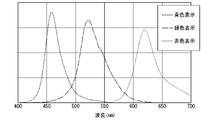
- FIG. 3 is a schematic cross-sectional view of an optical film 1B according to a third embodiment of the invention. It is a schematic cross section of the optical film 1C which concerns on 4th embodiment of this invention. It is a schematic cross section of optical film 1D which concerns on 5th embodiment of this invention. It is a spectrum of a light source used for evaluation of transmission characteristics. It is the spectrum of the light source used for evaluation of color reproducibility.
- FIG. 1 is a schematic cross-sectional view of an optical film 1 according to this embodiment.
- the optical film 1 includes a sheet-shaped transparent base material 10, a colored layer 30 containing a dye formed on the first surface 10a side of the transparent base material 10, and an optical functional layer 20 formed on the colored layer 30. and
- the transparent base material 10 may be simply referred to as the base material 10 in some cases.
- the direction in which the substrate 10, the colored layer 30, and the optical function layer 20 are laminated is referred to as the thickness direction, and one side in the thickness direction (observation side when observing the display image of the display device) is The upper side is called the upper side, and the opposite side is called the lower side.
- the base material 10 is made of a material that is highly transparent to visible light.
- Materials for forming the substrate 10 include polyolefins such as polyethylene and polypropylene; polyesters such as polyethylene terephthalate, polybutylene terephthalate and polyethylene naphthalate; polyacrylates such as polymethyl methacrylate; polyamides such as nylon 6 and nylon 66; Transparent resins such as arylate, polycarbonate, triacetylcellulose, polyacrylate, polyvinyl alcohol, polyvinyl chloride, cycloolefin copolymer, norbornene-containing resin, polyethersulfone, and polysulfone, and inorganic glass can be used.
- a film made of polyethylene terephthalate (PET), a film made of triacetyl cellulose (TAC), a film made of polymethyl methacrylate (PMMA), and a film made of polyester can be preferably used.
- the thickness of the substrate 10 is not particularly limited, it is preferably 10 to 100 ⁇ m.
- the colored layer 30 contains a pigment for selectively absorbing the wavelength band of visible light.
- the colored layer 30 may have a structure in which a dye is contained in a base resin made of an active energy ray-curable resin.
- the pigment includes at least one of the first to third coloring material groups shown below.
- the type of colorant to be included is not limited to one type, and two or more types of colorant may be included.
- the first coloring material has a maximum absorption wavelength within the range of 470 nm to 530 nm, and a half width (full width at half maximum) of the absorption spectrum of 15 nm to 45 nm.
- the second coloring material has a maximum absorption wavelength within the range of 560 nm to 620 nm, and a half width (full width at half maximum) of the absorption spectrum of 15 nm to 55 nm.
- the third colorant has a wavelength of 650 to 800 nm with the lowest transmittance in the wavelength range of 400 to 800 nm.
- the half width of the absorption spectrum refers to the full width at half maximum.
- the colored layer 30 has an absorption such that the transmittance of the maximum absorption wavelength in one of the absorption wavelength bands of the coloring material is 1% or more and less than 50%.
- the visible light emitted by the display device has a wavelength range with relatively low emission intensity. Visible light can be absorbed by the colored layer 30 .
- the visible light in the wavelength range of 400 to 800 nm, respectively, in the ranges of 470 nm to 530 nm, 560 nm to 620 nm, and 650 to 800 nm is colored. 30 can be absorbed.
- the wavelengths absorbed by the first, second, and third colorants are relatively It is a range that overlaps with the wavelength range where the emission intensity is low.
- the display device is not limited to the organic EL display device, and other display devices may be used.
- the colored layer 30 may contain at least one of a radical scavenger, a singlet oxygen quencher and a peroxide decomposer.
- the colorant contained in the colored layer 30 is also degraded by light, heat, etc. accelerated under the influence of oxygen.
- the highly reactive singlet oxygen which tends to cause oxidative deterioration (fading) of the dye, is deactivated, thereby suppressing oxidative deterioration (fading) of the dye. can do.
- the peroxide decomposer When the peroxide decomposer is mixed in the colored layer 30, the peroxide decomposer decomposes the peroxide generated when the pigment is oxidized and deteriorated, so that the auto-oxidation cycle is stopped and the pigment deterioration (fading) is prevented. can be suppressed.
- a radical scavenger and a singlet oxygen quencher may be used in combination. Additionally, a peroxide decomposer may be combined.
- a hindered amine light stabilizer can be used as a radical scavenger.
- a hindered amine light stabilizer having a molecular weight of 2,000 or more is particularly preferred because it provides a high effect of suppressing fading.
- the molecular weight of the radical scavenger is low, it is likely to volatilize, so few molecules remain in the colored layer 30, and it may be difficult to obtain a sufficient anti-fading effect.
- Examples of materials suitably used as radical scavengers include Chimassorb 2020FDL, Chimassorb 944FDL, Tinuvin 622 manufactured by BASF, and LA-63P manufactured by ADEKA.
- singlet oxygen quenchers include transition metal complexes, dyes, amines, phenols, and sulfides, and particularly preferably used materials include dialkyl phosphate, dialkyldithiocarbanate, benzenedithiol, or the like. Transition metal complexes of dithiols can be exemplified, and nickel, copper or cobalt is preferably used as the central metal of these transition metal complexes.
- the peroxide decomposer decomposes the peroxide that is generated when the pigment is oxidatively deteriorated, stops the auto-oxidation cycle, and suppresses pigment deterioration (fading).
- Phosphorus-based antioxidants and sulfur-based antioxidants can be used as peroxide decomposers.
- Phosphorus antioxidants include, for example, 2,2′-methylenebis(4,6-di-t-butyl-1-phenyloxy)(2-ethylhexyloxy)phosphorus, 3,9-bis(2,6-di -tert-butyl-4-methylphenoxy)-2,4,8,10-tetraoxa-3,9-diphosphaspiro[5.5]undecane, and 6-[3-(3-t-butyl-4-hydroxy- 5-methylphenyl)propoxy]-2,4,8,10-tetra-t-butyldibenz[d,f][1,3,2]dioxaphosphepine and the like.
- sulfur-based antioxidants examples include 2,2-bis( ⁇ [3-(dodecylthio)propionyl]oxy ⁇ methyl)-1,3-propanediyl-bis[3-(dodecylthio)propionate], 2-mercaptobenz imidazole, dilauryl-3,3'-thiodipropionate, dimyristyl-3,3'-thiodipropionate, distearyl-3,3'-thiodipropionate, pentaerythrityl-tetrakis(3-laurylthiopropionate pionate), 2-mercaptobenzothiazole, and the like.
- the optical function layer 20 shown in FIG. 1 has a hard coat layer 21 in contact with the colored layer 30 and a low refractive index layer 22 formed on the hard coat layer 21 .
- the hard coat layer 21 is a hard resin layer and enhances the scratch resistance of the optical film 1 . Moreover, the hard coat layer 21 may have a higher refractive index than the low refractive index layer 22 .
- the resin constituting the hard coat layer 21 is a resin that is polymerized and cured by irradiation with active energy rays such as ultraviolet rays and electron beams. Available.
- active energy rays such as ultraviolet rays and electron beams.
- active energy rays such as ultraviolet rays and electron beams. Available.
- (meth)acrylate is a generic term for both acrylate and methacrylate
- (meth)acryloyl is a generic term for both acryloyl and methacryloyl.
- Examples of monofunctional (meth)acrylate compounds include 2-hydroxyethyl (meth)acrylate, 2-hydroxypropyl (meth)acrylate, 2-hydroxybutyl (meth)acrylate, n-butyl (meth)acrylate, isobutyl ( meth)acrylate, t-butyl (meth)acrylate, glycidyl (meth)acrylate, acryloylmorpholine, N-vinylpyrrolidone, tetrahydrofurfuryl acrylate, cyclohexyl (meth)acrylate, 2-ethylhexyl (meth)acrylate, isobornyl (meth)acrylate ) acrylate, isodecyl (meth) acrylate, lauryl (meth) acrylate, tridecyl (meth) acrylate, cetyl (meth) acrylate, stearyl (meth) acrylate, benzyl (meth) acrylate,
- bifunctional (meth)acrylate compounds include ethylene glycol di(meth)acrylate, diethylene glycol di(meth)acrylate, butanediol di(meth)acrylate, hexanediol di(meth)acrylate, nonanediol di(meth) acrylates, ethoxylated hexanediol di(meth)acrylate, propoxylated hexanediol di(meth)acrylate, diethylene glycol di(meth)acrylate, polyethylene glycol di(meth)acrylate, tripropylene glycol di(meth)acrylate, polypropylene glycol di( Di(meth)acrylates such as meth)acrylate, neopentyl glycol di(meth)acrylate, ethoxylated neopentyl glycol di(meth)acrylate, tripropylene glycol di(meth)acrylate, and neopentylglycol
- tri- or higher functional (meth)acrylate compounds include trimethylolpropane tri(meth)acrylate, ethoxylated trimethylolpropane tri(meth)acrylate, propoxylated trimethylolpropane tri(meth)acrylate, and tris-2-hydroxyethyl.
- Tri(meth)acrylates such as isocyanurate tri(meth)acrylate, glycerin tri(meth)acrylate, pentaerythritol tri(meth)acrylate, dipentaerythritol tri(meth)acrylate, ditrimethylolpropane tri(meth)acrylate, etc.) Functional (meth)acrylate compounds, pentaerythritol tetra(meth)acrylate, ditrimethylolpropane tetra(meth)acrylate, dipentaerythritol tetra(meth)acrylate, dipentaerythritol penta(meth)acrylate, ditrimethylolpropane penta(meth)acrylate, ) acrylate, dipentaerythritol hexa (meth) acrylate, ditrimethylolpropane hexa (meth) acrylate trifunctional or higher polyfunctional (meth) acrylate compounds,
- Urethane (meth)acrylate can also be used as an active energy ray-curable resin.
- urethane (meth)acrylates include those obtained by reacting a product obtained by reacting a polyester polyol with an isocyanate monomer or a prepolymer with a (meth)acrylate monomer having a hydroxyl group. .
- urethane (meth)acrylates examples include pentaerythritol triacrylate hexamethylene diisocyanate urethane prepolymer, dipentaerythritol pentaacrylate hexamethylene diisocyanate urethane prepolymer, pentaerythritol triacrylate toluene diisocyanate urethane prepolymer, dipentaerythritol pentaacrylate toluene diisocyanate.
- Examples include urethane prepolymers, pentaerythritol triacrylate isophorone diisocyanate urethane prepolymers, and dipentaerythritol pentaacrylate isophorone diisocyanate urethane prepolymers.
- the resins described above may be used alone or in combination of two or more. Further, the above resin may be a monomer in the composition for forming a hard coat layer, or may be a partially polymerized oligomer.
- the hard coat layer 21 preferably has a pencil hardness of H or higher with a load of 500 g on the surface.
- the hard coat layer 21 contains an ultraviolet absorber in order to suppress deterioration of the dye contained in the colored layer 30 . Thereby, the hard coat layer 21 also becomes an ultraviolet shielding layer having an ultraviolet shielding rate of 85% or more.
- the UV shielding rate is a value measured according to JIS L 1925, and calculated by the following formula.
- Ultraviolet shielding rate (%) 100 - average transmittance of ultraviolet rays with a wavelength of 290 to 400 nm (%)
- the absorption wavelength range of the ultraviolet absorber contained in the hard coat layer 21 in the ultraviolet region is preferably in the range of 290 to 370 nm.
- ultraviolet absorbers include benzophenone-based, benzotriazole-based, triazine-based, oxalic acid anilide-based, and cyanoacrylate-based compounds.
- the ultraviolet absorber is blended in order to suppress deterioration of pigments contained in the colored layer 30 . For this reason, an ultraviolet absorber is used that absorbs light in the wavelength range that contributes to the deterioration of the dye contained in the colored layer 30 in the ultraviolet region.
- the hard coat layer 21 is a UV shielding layer (UV absorption layer), and an ultraviolet absorber whose absorption wavelength range in the ultraviolet region is different from the absorption wavelength region in the ultraviolet region of the photopolymerization initiator is used.
- UV absorption layer UV absorption layer
- acyl A phosphine oxide-based photopolymerization initiator can be preferably used.
- acylphosphine oxide-based photopolymerization initiators include diphenyl(2,4,6-trimethylbenzoyl)phosphine oxide and phenylbis(2,4,6-trimethylbenzoyl)phosphine oxide.
- the absorption wavelength regions of the ultraviolet absorber and the photopolymerization initiator By making the absorption wavelength regions of the ultraviolet absorber and the photopolymerization initiator different, it is possible to suppress curing inhibition when forming the ultraviolet shielding layer containing the ultraviolet absorber, and after curing, it is included in the colored layer 30. It is possible to suppress the deterioration of the pigment that is applied by ultraviolet rays.
- photopolymerization initiators used in the hard coat layer-forming composition include, for example, 2,2-ethoxyacetophenone, 1-hydroxycyclohexylphenyl ketone, dibenzoyl, benzoin, benzoin methyl ether, benzoin ethyl ether, p-chloro Benzophenone, p-methoxybenzophenone, Michler's ketone, acetophenone, 2-chlorothioxanthone and the like can be used.
- One type of these may be used alone, or two or more types may be used in combination.
- Solvents used in the hard coat layer-forming composition include dibutyl ether, dimethoxymethane, dimethoxyethane, diethoxyethane, propylene oxide, 1,4-dioxane, 1,3-dioxolane, and 1,3,5-trioxane.
- Ethers such as , tetrahydrofuran, anisole and phenetole, and ketones such as acetone, methyl ethyl ketone, diethyl ketone, dipropyl ketone, diisobutyl ketone, methyl isobutyl ketone, cyclopentanone, cyclohexanone, methylcyclohexanone and methylcyclohexanone, and ethyl formate.
- ketones such as acetone, methyl ethyl ketone, diethyl ketone, dipropyl ketone, diisobutyl ketone, methyl isobutyl ketone, cyclopentanone, cyclohexanone, methylcyclohexanone and methylcyclohexanone, and ethyl formate.
- composition for forming a hard coat layer may contain metal oxide fine particles for the purpose of adjusting the refractive index and imparting hardness.
- Metal oxide fine particles include zirconium oxide, titanium oxide, niobium oxide, antimony trioxide, antimony pentoxide, tin oxide, indium oxide, indium tin oxide, and zinc oxide.
- composition for forming a hard coat layer includes a silicon oxide, a fluorine-containing silane compound, a fluoroalkylsilazane, a fluoroalkylsilane, a fluorine-containing silicon-based compound, which imparts water repellency and/or oil repellency and enhances antifouling properties.
- Any perfluoropolyether group-containing silane coupling agent may be contained.
- a leveling agent As other additives, a leveling agent, an antifoaming agent, an antioxidant, a light stabilizer, a photosensitizer, a conductive material, etc. may be added to the composition for forming the hard coat layer.
- the low refractive index layer 22 is arranged on the side closest to the user (viewer) viewing the display when the optical film 1 is applied to the display device.
- the low refractive index layer 22 prevents strong reflection of external light and improves the visibility of the display device.
- the low refractive index layer 22 may be a layer containing an inorganic substance or an inorganic compound.
- inorganic substances and inorganic compounds include fine particles such as LiF, MgF, 3NaF.AlF, AlF, Na 3 AlF 6 and silica fine particles.
- silica fine particles have voids inside the particles such as porous silica fine particles and hollow silica fine particles, it is effective in lowering the refractive index of the low refractive index layer.
- the composition for forming the low refractive index layer may appropriately contain the photopolymerization initiator, solvent, and other additives described for the hard coat layer 21 .
- the refractive index of the low refractive index layer 22 should be lower than the refractive index of the substrate 10, preferably 1.55 or less. Also, the film thickness of the low refractive index layer 22 is not particularly limited, but is preferably 40 nm to 1 ⁇ m.
- the low refractive index layer 22 may contain any one of silicon oxide, fluorine-containing silane compound, fluoroalkylsilazane, fluoroalkylsilane, fluorine-containing silicon-based compound, and perfluoropolyether group-containing silane coupling agent. These materials can impart water repellency and/or oil repellency to the low refractive index layer 22, thereby enhancing antifouling properties.
- the optical film 1 can be produced by forming the colored layer 30 on the first surface 10a of the substrate 10, and then forming the hard coat layer 21 and the low refractive index layer 22 on the colored layer 30 in this order.
- the colored layer 30, the hard coat layer 21, and the low refractive index layer 22 can be formed, for example, by applying a coating liquid containing constituent materials of each layer and drying.
- the low refractive index layer 22 can be formed by vapor deposition, sputtering, or the like, for example.
- the hard coat layer 21 can be easily formed by forming the hard coat layer 21 with an energy ray curable compound such as an ultraviolet curable resin.
- the hard coat layer 21 can be formed by applying a coating liquid containing an energy ray-curable compound, a polymerization initiator, and an ultraviolet absorber, and irradiating the corresponding energy ray.
- an ultraviolet curable resin is used, as described above, the absorption wavelength range of the photopolymerization initiator in the ultraviolet region is preferably different from the absorption wavelength range of the ultraviolet absorber in the ultraviolet region.
- the optical film 1 can be arranged inside a display device such as a display as a color correction filter.
- a display device such as a display as a color correction filter.
- the second surface (10b shown in FIG. 1) opposite to the first surface 10a of the base material 10 is arranged toward the light source side.
- the wavelength components near the maximum absorption wavelength of the included colorant are absorbed.
- the color purity of the display device can be improved.
- the colorant contained in the colored layer 30 has an excellent color correction function, it may not have sufficient resistance to light rays, particularly ultraviolet rays. Therefore, when irradiated with ultraviolet rays, it deteriorates over time and becomes unable to absorb light in the vicinity of the maximum absorption wavelength.
- the optical film 1 of the present embodiment is attached to the display device as described above, external light including ultraviolet rays entering the display screen passes through the hard coat layer 21 and then enters the colored layer 30 . Since the hard coat layer 21 has a high ultraviolet shielding rate, most of the ultraviolet rays contained in the outside light do not pass through the hard coat layer 21 and do not reach the colored layer 30 .
- ⁇ E*ab which is the chromaticity difference before and after the light resistance test (xenon lamp illuminance 60 W/cm 2 (300 to 400 nm), temperature 45° C., humidity 50% RH, irradiation for 120 hours) is the following formula (1): ⁇ E*ab ⁇ 5 Formula (1) can satisfy That is, it is possible to prevent deterioration of the coloring material contained in the colored layer 30, and to maintain the color correction function for a long time.
- ⁇ E*ab in Equation (1) is a chromaticity difference standardized by CIE (Commission international de l'eclairage).
- FIG. 2 is a schematic cross-sectional view showing the layer structure of the optical film 1A of this embodiment.
- the optical film 1A includes a transparent base material 10, a colored layer 30 containing a pigment formed on the first surface 10a side of the base material 10, and an optical function layer 20 formed on the colored layer 30.
- the optical film 1 ⁇ /b>A includes an antiglare layer (Anti Glare Layer: AG layer) 23 as the optical functional layer 20 .
- the optical function layer 20 has an ultraviolet shielding layer, and may have a layer containing the ultraviolet absorber described in the first embodiment, or the antiglare layer 23 may contain an ultraviolet absorber. .
- the ultraviolet shielding rate of the ultraviolet shielding layer conforming to JIS L 1925 is 85% or more.
- the anti-glare layer 23 is a layer that has fine irregularities on its surface, and reduces reflection of external light by scattering external light with these irregularities.
- the antiglare layer 23 can be formed by applying and curing an antiglare layer forming composition containing an active energy ray-curable resin and, if necessary, organic fine particles and/or inorganic fine particles.
- the active energy ray-curable resin used in the composition for forming the antiglare layer the resin described for the hard coat layer 21 can be used. Thereby, the scratch resistance of the optical film 1A can be improved.
- the film thickness of the antiglare layer 23 is not particularly limited, it is preferably 1 to 10 ⁇ m.
- the organic fine particles used in the composition for forming the antiglare layer are mainly a material that forms fine irregularities on the surface of the antiglare layer 23 and imparts the function of diffusing external light.
- translucent resin materials such as acrylic resins, polystyrene resins, styrene-(meth)acrylic acid ester copolymers, polyethylene resins, epoxy resins, silicone resins, polyvinylidene fluoride, and polyethylene fluoride resins are used. Resin particles can be used. In order to adjust the refractive index and the dispersibility of the resin particles, two or more kinds of resin particles having different materials (refractive indexes) may be mixed and used.
- the inorganic fine particles used in the composition for forming the antiglare layer are mainly materials for adjusting the sedimentation and aggregation of the organic fine particles in the antiglare layer 23 .
- silica fine particles, metal oxide fine particles, various mineral fine particles, and the like can be used.
- silica fine particles that can be used include colloidal silica and silica fine particles surface-modified with reactive functional groups such as (meth)acryloyl groups.
- metal oxide fine particles that can be used include alumina, zinc oxide, tin oxide, antimony oxide, indium oxide, titania, and zirconia.
- Mineral fine particles include, for example, mica, synthetic mica, vermiculite, montmorillonite, iron montmorillonite, bentonite, beidellite, saponite, hectorite, stevensite, nontronite, magadiite, islarite, kanemite, layered titanate, smectite, synthetic Smectite and the like can be used.
- Mineral fine particles may be either natural products or synthetic products (including substituted products and derivatives), and a mixture of both may be used.
- layered organoclays are more preferred.
- a layered organic clay is a swelling clay in which organic onium ions are introduced between layers.
- the organic onium ion is not limited as long as it can be organicized by utilizing the cation exchange property of the swelling clay.
- the synthetic smectite described above can be preferably used. Synthetic smectite has the function of increasing the viscosity of the coating liquid for forming the antiglare layer, suppressing the sedimentation of resin particles and inorganic fine particles, and adjusting the irregular shape of the surface of the optical function layer.
- the antiglare layer-forming composition may contain any one of silicon oxide, fluorine-containing silane compound, fluoroalkylsilazane, fluoroalkylsilane, fluorine-containing silicon-based compound, and perfluoropolyether group-containing silane coupling agent. good. Since these materials can impart water repellency and/or oil repellency to the antiglare layer 23, antifouling properties can be enhanced.
- the anti-glare layer 23 is formed as a layer in which a layer with a relatively high refractive index and a layer with a relatively low refractive index are laminated in order from the colored layer 30 side (lower side) by unevenly distributing the material. You may
- the anti-glare layer 23 in which the materials are unevenly distributed is formed by, for example, coating a composition containing a low refractive index material containing surface-modified silica fine particles or hollow silica fine particles and a high refractive index material. It can be formed by phase separation using the energy difference.
- the refractive index of the layer with a relatively high refractive index on the colored layer 30 side is set to 1.50 to 2.40, and the refractive index of the layer on the surface side of the optical film 1A is set to 1.50 to 2.40. It is preferable that the refractive index of the layer having the lowest refractive index is 1.20 to 1.55.
- the optical film 1A can be manufactured by forming the colored layer 30 on the first surface 10a of the substrate 10 and then forming the antiglare layer 23 on the colored layer 30 in sequence.
- the antiglare layer 23 can be formed, for example, by applying a coating liquid containing constituent materials of each layer and drying the coating liquid.
- the optical film 1A according to the present embodiment can reduce the reflection of external light while preventing deterioration of the coloring material contained in the colored layer 30 in the same manner as in the above-described first embodiment.
- FIG. 3 is a schematic cross-sectional view showing the layer structure of the optical film 1B of this embodiment.
- the optical film 1B includes a transparent base material 10, a colored layer 30 containing a dye formed on the first surface 10a side of the base material 10, and an optical functional layer 20 formed on the colored layer 30.
- the optical film 1 ⁇ /b>B includes a hard coat layer 21 as an optical functional layer 20 and an antiglare layer 23 formed on the hard coat layer 21 .
- the optical function layer 20 has an ultraviolet shielding layer and may have a layer containing the ultraviolet absorber described in the first embodiment. It may be In addition, the ultraviolet shielding rate of the ultraviolet shielding layer conforming to JIS L 1925 is 85% or more.
- the optical film 1B can be produced by forming the colored layer 30 on the first surface 10a of the substrate 10, and then forming the hard coat layer 21 and the antiglare layer 23 on the colored layer 30 in this order.
- the optical film 1 ⁇ /b>B according to this embodiment has the same effects as those of the above-described embodiments, and can exhibit optical functions based on the optical function layer 20 .
- FIG. 4 is a schematic cross-sectional view showing the layer structure of the optical film 1C of this embodiment.
- the optical film 1C includes a transparent base material 10, a colored layer 30 containing a pigment formed on the first surface 10a side of the base material 10, and an optical functional layer 20 formed on the colored layer 30.
- the optical film 1 ⁇ /b>C includes an antiglare layer 23 as an optical functional layer 20 and a low refractive index layer 22 formed on the antiglare layer 23 .
- the optical function layer 20 has an ultraviolet shielding layer and may have a layer containing the ultraviolet absorber described in the first embodiment. may be included.
- the ultraviolet shielding rate of the ultraviolet shielding layer conforming to JIS L 1925 is 85% or more.
- the optical film 1C can be manufactured by forming the colored layer 30 on the first surface 10a of the substrate 10, and then forming the antiglare layer 23 and the low refractive index layer 22 on the colored layer 30 in this order.
- the optical film 1 ⁇ /b>C according to this embodiment can exhibit the same effects as those of the above-described embodiments, and can exhibit optical functions based on the optical function layer 20 .
- FIG. 5 is a schematic cross-sectional view showing the layer structure of the optical film 1D of this embodiment.
- the optical film 1D includes a transparent base material 10, a colored layer 30 containing a dye formed on the first surface 10a side of the base material 10, and an optical function layer 20 formed on the colored layer 30.
- the optical film 1D includes an oxygen barrier layer 40 as the optical functional layer 20, a hard coat layer 21 formed on the oxygen barrier layer 40, and a low refractive index layer 22 formed on the hard coat layer 21.
- the optical function layer 20 has an ultraviolet shielding layer, may have a layer containing the ultraviolet absorber described in the first embodiment, or may include an oxygen barrier layer 40, a hard coat layer 21, or a low refractive index layer. 22 may contain a UV absorber.
- the ultraviolet shielding rate of the ultraviolet shielding layer conforming to JIS L 1925 is 85% or more.
- the oxygen barrier layer 40 is a transparent layer having optical transparency, and has an oxygen permeability of 10 cc/(m 2 ⁇ day ⁇ atm) or less, preferably 5 cc/(m 2 ⁇ day ⁇ atm) or less. It is more preferably 1 cc/(m 2 ⁇ day ⁇ atm) or less.
- the material for forming the oxygen barrier layer 40 preferably contains polyvinyl alcohol (PVA), ethylene-vinyl alcohol copolymer (EVOH), vinylidene chloride, siloxane resin, etc. Maxieve (registered trademark) manufactured by Mitsubishi Gas Chemical Company, Inc. , EVAL manufactured by Kuraray Co., Ltd., Saran Latex and Saran Resin manufactured by Asahi Kasei Corporation can be used.
- the thickness of the oxygen barrier layer 40 is not particularly limited, and may be a thickness that provides desired oxygen barrier properties.
- Inorganic particles may also be dispersed in the oxygen barrier layer 40 .
- Oxygen permeability can be further reduced by the inorganic particles, and oxidative deterioration (discoloration) of the colored layer 30 can be further suppressed.
- the size and content of the inorganic particles are not particularly limited, and may be appropriately set according to the thickness of the oxygen barrier layer 40 and the like.
- the size (maximum length) of the inorganic particles dispersed in the oxygen barrier layer 40 is preferably less than the thickness of the oxygen barrier layer 40, and the smaller the better.
- the size of the inorganic particles dispersed in the oxygen barrier layer 40 may be uniform or non-uniform. Specific examples of inorganic particles dispersed in the oxygen barrier layer 40 include silica particles, alumina particles, silver particles, copper particles, titanium particles, zirconia particles, tin particles, and the like.
- the optical film 1D can be produced by forming the colored layer 30 on the first surface 10a of the substrate 10, and sequentially forming the oxygen barrier layer 40, the hard coat layer 21, and the low refractive index layer 22 on the colored layer 30. .
- the number and positions of the oxygen barrier layers 40 can be set as appropriate.
- the oxygen barrier layer 40 may be laminated on the observer side above the colored layer 30 .
- an oxygen barrier layer 40 may be further provided between the colored layer 30 and the antiglare layer 23 .
- an oxygen barrier layer 40 is further provided between the colored layer 30 and the hard coat layer 21 or between the hard coat layer 21 and the antiglare layer 23. good too.
- another oxygen barrier layer may be provided between the colored layer 30 and the substrate 10, and the colored layer 30 may be sandwiched between the oxygen barrier layers.
- the optical function layer 20 is not limited to the configuration described above.
- an antireflection layer in which a plurality of low refractive index layers and high refractive index layers are combined is also an example of the optical function layer 20 in the present invention.
- the resin used for the composition for forming the high refractive index layer the active energy ray-curable resin described for the hard coat layer 21 may be used. Thereby, in addition to the function of preventing reflection, the scratch resistance of the optical film can be enhanced.
- optical film according to the present invention will be further explained using examples and comparative examples.
- the present invention is not limited at all by the specific contents of each of the following examples.
- Dye-1 Pyromethene cobalt complex dye represented by chemical formula 1 described later (maximum absorption wavelength 493 nm, half width 26 nm)
- ⁇ Second coloring material Dye-2 tetraazaporphyrin copper complex dye (FDG-007 manufactured by Yamada Chemical Co., Ltd., maximum absorption wavelength 595 nm, half width 22 nm)
- Dye-3 Tetraazaporphyrin copper complex dye (PD-311S manufactured by Yamamoto Kasei Co., Ltd., maximum absorption wavelength 586 nm, half width 22 nm)
- Dye-4 phthalocyanine copper complex dye (FDN-002 manufactured by Yamada Chemical Co., Ltd., maximum absorption wavelength 800 nm (800 nm is the wavelength with the lowest transmittance in the wavelength range of 400 to 800 nm))
- Dye-5 dye (FDG-003 manufactured by Yamada
- a triacetyl cellulose film (TAC) having a thickness of 60 ⁇ m was used as a transparent substrate, and the composition for forming a colored layer shown in Table 4 was applied to one side of the transparent substrate and dried in an oven at 80° C. for 60 seconds. rice field. After that, the coating film is cured by performing ultraviolet irradiation with an irradiation dose of 150 mJ/cm 2 (manufactured by Fusion UV Systems Japan, light source H bulb) using an ultraviolet irradiation device, and the film thickness after curing becomes 5.0 ⁇ m. Colored layers 1 to 10 were formed by adjusting the thickness as follows. In addition, the addition amount is a mass ratio.
- the composition for forming an oxygen barrier layer was applied onto the colored layer and dried to form an oxygen barrier layer 1 shown in Table 1 having an oxygen permeability of 1 cc/(m 2 ⁇ day ⁇ atm).
- composition for forming hard coat layer The materials used in the composition for forming a hard coat layer were used for forming the hard coat layer described below.
- ⁇ Ultraviolet absorber Tinuvin479 (manufactured by BASF Japan, maximum absorption wavelength 322 nm)
- LA-36 manufactured by ADEKA, maximum absorption wavelength 310 nm, 350 nm
- ⁇ Active energy ray curable resin UA-306H (manufactured by Kyoeisha Chemical Co., Ltd., pentaerythritol triacrylate hexamethylene diisocyanate urethane prepolymer)
- DPHA dipentaerythritol hexaacrylate
- PETA penentaerythritol triacrylate
- ⁇ Initiator Omnirad TPO (manufactured by IGM Resins B.V., absorption wavelength peaks 275 nm, 379 nm) Omnirad 184 (man
- the composition for forming a hard coat layer shown in Table 5 is applied onto the colored layer, the transparent substrate, or the oxygen barrier layer 1, dried in an oven at 80°C for 60 seconds, and then irradiated with an ultraviolet irradiation device.
- the hard coat layer 1 in Tables 1 and 2 having a thickness of 5.0 ⁇ m after curing is cured by irradiating with ultraviolet rays (light source H bulb, manufactured by Fusion UV Systems Japan) at a dose of 150 mJ/cm 2 . ⁇ 3 were formed. Since the hard coat layers 1 and 3 contain an ultraviolet absorber, they also serve as ultraviolet shielding layers.
- composition for forming antiglare layer The following materials were used as the antiglare layer-forming composition for forming the antiglare layer.
- ⁇ Ultraviolet absorber Tinuvin479 (manufactured by BASF Japan, maximum absorption wavelength 322 nm)
- LA-36 manufactured by ADEKA, maximum absorption wavelength 310 nm, 350 nm
- ⁇ Active energy ray curable resin Light acrylate PE-3A (manufactured by Kyoeisha Chemical Co., Ltd., refractive index 1.52)
- Photoinitiator Omnirad TPO (manufactured by IGM Resins B.V., absorption wavelength peaks 275 nm, 379 nm)
- Organic fine particles Styrene-methyl methacrylate copolymer particles (refractive index 1.515, average particle size 2.0 ⁇ m)
- Inorganic fine particles 1 Synthetic smectite/inorganic fine particles 2: A
- the composition for forming an antiglare layer shown in Table 6 is applied onto the layer structure shown in Table 1, dried in an oven at 80 ° C. for 60 seconds, and then using an ultraviolet irradiation device.
- the coating film is cured by irradiating with ultraviolet rays (light source H bulb manufactured by Fusion UV Systems Japan Co., Ltd.) at an irradiation dose of 150 mJ/cm 2 to form the antiglare layer shown in Table 1 with a film thickness of 5.0 ⁇ m after curing. did. Since the antiglare layer 1 contains an ultraviolet absorber, it also serves as an ultraviolet shielding layer.
- composition for forming low refractive index layer The following materials were used as the composition for forming a low refractive index layer.
- ⁇ Refractive index adjuster Porous silica fine particle dispersion (average particle diameter 75 nm, solid content 20%, solvent methyl isobutyl ketone) 8.5 parts by mass
- Antifouling agent Optool AR-110 (manufactured by Daikin Industries, Ltd., solid content 15%, solvent methyl isobutyl ketone) 5.6 parts by mass
- Active energy ray curable resin Pentaerythritol triacrylate 0.4 parts by mass Initiator: Omnirad 184 (manufactured by IGM Resins B.V.) 0.07 parts by mass
- Solvent Methyl isobutyl ketone 83.73 parts by mass
- the composition for forming a low refractive index layer having the above composition is applied and dried in an oven at 80 ° C. for 60 seconds, and then an ultraviolet irradiation device (Fusion UV Systems Japan Co., Ltd., light source
- the coating film was cured by irradiating with ultraviolet rays at an irradiation dose of 200 mJ/cm 2 using an H bulb) to form the low refractive index layers shown in Tables 1 and 2 having a film thickness of 100 nm after curing.
- the ultraviolet shielding layer (ultraviolet absorbing layer) formed on the colored layer of the obtained optical film was peeled off from the colored layer using cellophane tape conforming to the JIS-K5600 adhesion test, and the ultraviolet shielding layer alone was placed on the cellophane tape. The layer was transferred.
- the ultraviolet shielding layer (ultraviolet absorbing layer) of the optical film is a layer containing an ultraviolet absorbent among the optical functional layers, and includes the hard coat layers 1 and 3 and the antiglare layer 1 . Tables 7 and 8 show the ultraviolet shielding layer (ultraviolet absorbing layer) contained in each optical film.
- the transmittance of the single layer of the ultraviolet shielding layer is measured using an automatic spectrophotometer (U-4100, manufactured by Hitachi, Ltd.), and measured in the ultraviolet region (290 to 400 nm). was calculated. The obtained average transmittance was used to calculate the ultraviolet shielding rate shown in Equation (2).
- Ultraviolet shielding rate (%) 100 - average transmittance (%) in the ultraviolet region (290 to 400 nm)
- Transmittance is measured using an automatic spectrophotometer (U-4100, manufactured by Hitachi, Ltd.) before and after the test, and the wavelength showing the minimum transmittance in the absorption wavelength range of the first to third colorants
- U-4100 automatic spectrophotometer
- a transmittance difference ⁇ T ⁇ before and after the test at ⁇ and a color difference ⁇ E*ab with a C light source before and after the test were calculated.
- Transmittance difference and color difference close to zero are preferable, and ⁇ E*ab ⁇ 5 is preferable.
- Display device characteristic evaluation In Examples 8 to 11 and Comparative Examples 7 to 10 below, display device characteristics of the display devices using the obtained optical films 8, 10, 11, and 18 to 21 were evaluated by simulation as follows. In the simulation, the display device had a configuration in which an optical film was bonded to an organic EL display device (object). In the organic EL display device, which is the object to which the optical film is bonded, the spectral spectrum is as shown in FIG. 6 during white display, and the single spectrum as shown in FIG. Become. (Transmission characteristics (white display transmission characteristics)) The transmittance of the obtained optical film was measured using an automatic spectrophotometer (U-4100, manufactured by Hitachi, Ltd.).
- the spectral spectrum after transmission through the optical film was calculated by multiplying the individual spectral spectra during white display of the EL display device.
- the Y value is calculated by multiplying the spectrum of the organic EL display device when white is displayed alone and the spectral spectrum after transmission of the optical film by the relative luminosity, and the spectrum of the organic EL display device when white is displayed alone. Efficiency was defined as the ratio when the Y value obtained from the above was 100, and was evaluated as an index of the transmission characteristics of the display device.
- DCI Digital Cinema Initiatives
- Tables 7 and 8 show the results of the UV shielding rate, pencil hardness, and light resistance test of the UV shielding layer (UV absorbing layer) as the optical film property evaluation of the optical films 1 to 17 shown in Tables 1 and 2.
- the optical films of Examples 1 to 11 are provided with a colored layer and an optical functional layer having an ultraviolet absorbing ability disposed above the colored layer.
- the UV shielding rate of the optical functional layer having UV absorption ability disposed above the colored layer is 85% or more. From the results in Tables 7 and 8, the optical films (Examples 1 to 11) provided with a colored layer according to the present invention were not provided with ultraviolet absorption ability as in Comparative Examples 1, 2, 5 and 6, and in Comparative Example 3.
- the light resistance of the colored layer is significantly improved, compared with the case where it is provided in the colored layer.
- the determination of pencil hardness is "OK".
- the pencil hardness was judged as "NG”. This is probably because the absorption wavelength peak of the initiator of the hard coat layer 3 overlapped with the absorption wavelength of the ultraviolet absorber.
- the hard coat layer 1 or antiglare layer 1 included in Examples 1 to 11 is an ultraviolet shielding layer (ultraviolet absorption layer) formed of an active energy ray-curable resin containing an ultraviolet absorber. By shifting the absorption wavelength band of the polymerization initiator, it was possible to achieve both UV shielding ability and hardness.
- Table 9 shows the results of simulating white display transmission characteristics and color reproducibility as characteristic evaluations of display devices using optical films 8, 10, 11 and 18-21.
- the display device to which the optical film having the colored layer of the present invention was attached exhibited a DCI standard coverage rate of 90% or more, and compared to Comparative Example 7 without the colored layer, the color reproducibility was improved. did.
- the DCI chromaticity inclusion rate was greatly improved in Example 8, which has a large absorption in the wavelength band of the first colorant.
- Comparative Example 8 in which the first colorant and the second colorant have deep absorption in a plurality of wavelength bands, the white display transmission characteristic is low. Therefore, when the colored layer contains a plurality of types of colorants, the transmittance at only one of the maximum absorption wavelengths of the colorants should be 1% or more and less than 50%. is preferred.
- Comparative Examples 9 and 10 which use colorants whose wavelength range and half-value width do not conform to the regulations, have low color reproducibility evaluations.
- Examples 8 to 11 exhibited a certain color correction function and were also excellent in white display transmission characteristics.
- the optical film may include the colored layer 30 and the optical function layer 20 formed above the colored layer 30 and including a layer (ultraviolet shielding layer) having ultraviolet absorption capability.
- the layer having ultraviolet absorption ability may be the hard coat layer 21 or the antiglare layer 23 .
- the antiglare layer 23 may use the resins mentioned in the composition of the hard coat layer 21 in the first embodiment. That is, the optical function layer 20 may have a cured film of the composition containing the energy ray-curable compound, the photopolymerization initiator, and the ultraviolet absorber described in the first embodiment.
- the optical function layer 20 has a UV shielding rate of 85% or higher in accordance with JIS L 1925, and a surface pencil hardness of H or higher with a load of 500 g. This can improve the scratch resistance of the optical film while preventing deterioration of the coloring material contained in the colored layer 30 .
- desired functions may be imparted to the optical film of the present invention by providing another layer.
- other layers include an antistatic layer and an antifouling layer.
- an antistatic agent may be added to any layer of the optical functional layer 20 of the optical film to impart antistatic properties.
- Antifouling properties may be imparted by incorporating a material having water repellency and/or oil repellency into any layer of the optical function layer 20 .
- Optical film 10 Substrate (transparent substrate) 10a first surface 10b second surface 20 optical function layer 21 hard coat layer 22 low refractive index layer 23 antiglare layer 30 colored layer 40 oxygen barrier layer
Landscapes
- Physics & Mathematics (AREA)
- General Physics & Mathematics (AREA)
- Optics & Photonics (AREA)
- Chemical & Material Sciences (AREA)
- Health & Medical Sciences (AREA)
- Chemical Kinetics & Catalysis (AREA)
- Medicinal Chemistry (AREA)
- Polymers & Plastics (AREA)
- Organic Chemistry (AREA)
- Toxicology (AREA)
- Theoretical Computer Science (AREA)
- Engineering & Computer Science (AREA)
- Inorganic Chemistry (AREA)
- General Chemical & Material Sciences (AREA)
- Optical Filters (AREA)
Abstract
Description
本願は、2021年1月19日に日本に出願された特願2021-006751号に基づき優先権を主張し、その内容をここに援用する。
さらに、色純度を向上させたカラーフィルタは概して透過率が低く、輝度効率を低下させやすい。
特許文献1には、反射防止層及び電磁波遮断層を有するフィルタベース上に色補正層を設けたディスプレイフィルタが開示されている。このディスプレイフィルタは、反射防止フィルムに色補正層を設けた構成であるため、製造にフォトリソグラフィ工程は必要なく、輝度効率も低下しにくい。
特許文献2には、色補正層に適した色材が開示されている。
発明者らは、この問題の解決法について検討し、本発明を完成させた。
ΔE*ab≦5 式(1)
を満たす。
<第一実施形態>
図1は、本実施形態に係る光学フィルム1の模式断面図である。光学フィルム1は、シート状の透明基材10と、透明基材10の第一面10a側に形成された、色素を含有する着色層30と、着色層30上に形成された光学機能層20とを備えている。以降、透明基材10を単に基材10と呼ぶ場合もある。
本実施形態では、基材10、着色層30および光学機能層20が積層された方向を厚さ方向といい、厚さ方向における一方側(表示装置の表示画像を観察するときの観察側)を上側といい、その反対側を下側という。
色素は、以下に示す第一~第三の3種類の色材の群のうち少なくともいずれか一つを含む。含まれる色材の種類は一種類に限定されず、二種類以上の色材が含まれていてもよい。
第一の色材は、極大吸収波長が470nm~530nmの範囲内にあり、吸光スペクトルの半値幅(半値全幅)が15nm~45nmである。
第二の色材は、極大吸収波長が560nm~620nmの範囲内にあり、吸光スペクトルの半値幅(半値全幅)が15nm~55nmである。
第三の色材は、400~800nmの波長範囲において最も透過率の低い波長が650~800nmの範囲内にある。
なお、以降の説明において、吸光スペクトルの半値幅は、半値全幅を指す。
着色層30は、前記色材の吸収波長帯のうちいずれか1つの波長帯の極大吸収波長の透過率が1%以上50%未満となる吸収をもつ。
着色層30に含有させる第一乃至第三の色材として、上記の吸収特性を有する色材を使用することにより、表示装置が発光する可視光線のうち、相対的に発光強度が低い波長域の可視光線を着色層30に吸収させることができる。例えば、第一、第二、第三の色材により、400~800nmの波長範囲の可視光線のうち、それぞれ、470nm~530nm、560nm~620nm、650~800nmの範囲内にある可視光を着色層30に吸収させることができる。第一、第二、第三の色材により吸収される波長は、例えば、図6に示される有機EL表示装置の白表示時の分光スペクトルにおける表示装置が発光する可視光線のうち、相対的に発光強度が低い波長域と重なる範囲である。なお、表示装置は有機EL表示装置に限られず、その他の表示装置でもよい。
着色層30に含まれる色材は、酸素影響下で促進される光線、熱などによっても劣化する。ラジカル捕捉剤を着色層30に混合することにより、色素が酸化劣化する際のラジカルを捕捉して自動酸化による色材の劣化を防ぐことができ、色補正機能の持続時間をさらに長くすることができる。
また、一重項酸素クエンチャーを着色層30に混合することにより、色素を酸化劣化(退色)させやすい性質を持つ反応性の高い一重項酸素を不活性化し、色素の酸化劣化(退色)を抑制することができる。過酸化物分解剤を着色層30に混合した場合、色素が酸化劣化した際に発生する過酸化物を過酸化物分解剤が分解するため、自動酸化サイクルを停止させ、色素劣化(退色)を抑制できる。
ラジカル捕捉剤と一重項酸素クエンチャーとが併用されてもよい。さらに、過酸化物分解剤が組み合わされてもよい。
紫外線遮蔽率(%)=100-波長290~400nmの紫外線の平均透過率(%)
ただし、紫外線吸収剤を含有する組成物を硬化させる際、紫外線吸収剤による紫外線吸収量が多くなりすぎると、組成物の硬化が不十分となり、得られる光学フィルムの表面硬度が不足してしまう。
そこで、本実施形態においては、ハードコート層21(光学機能層20)が、エネルギー線硬化型化合物と光重合開始剤と紫外線吸収剤とを含有する組成物の硬化膜である紫外線遮蔽層(紫外線吸収層)を含み、紫外線領域における吸収波長域が、光重合開始剤の紫外線領域における吸収波長域と異なる範囲である紫外線吸収剤を使用する。これにより、紫外線吸収剤により硬化膜の硬化が阻害されることを抑制できる。また、硬化膜を所定の硬化度まで硬化させることができるため、確実に目的の硬度の硬化層を得ることができる。
紫外線遮蔽層を構成するいずれかの層に含有させる紫外線吸収剤の吸収波長域(着色層30に含まれる色素の劣化に寄与する波長域)とは吸収波長域が異なる光重合開始剤として、アシルフォスフィンオキサイド系の光重合開始剤を好適に使用することができる。アシルフォスフィンオキサイド系の光重合開始剤としては、ジフェニル(2,4,6-トリメチルベンゾイル)ホスフィンオキシドやフェニルビス(2,4,6-トリメチルベンゾイル)ホスフィンオキシドなどを例示できる。
紫外線吸収剤と光重合開始剤との吸収波長域を異ならせることにより、紫外線吸収剤を含有する紫外線遮蔽層を形成する際の硬化阻害を抑制できると共に、硬化後においては、着色層30に含まれる色素が紫外線により劣化することを抑制できる。
着色層30、ハードコート層21及び低屈折率層22は、例えば各層の構成材料を含む塗工液を塗工し、乾燥することで形成できる。また、低屈折率層22は、例えば、蒸着やスパッタリング等によっても形成できる。
光源から出射された光は、着色層30を透過する際に、含まれる色材の極大吸収波長付近の波長成分が吸収される。これにより、表示装置の色純度を向上できる。さらに、カラーフィルタと異なり、色材濃度をそれほど高くする必要がないため、表示装置の輝度を過度に低下させずに色純度を向上できる。
本実施形態の光学フィルム1が上述のように表示装置に取り付けられた場合、表示画面に入射する紫外線を含む外光は、ハードコート層21を透過してから着色層30に入射する。ハードコート層21は高い紫外線遮蔽率を有するため、外光に含まれる紫外線の大部分はハードコート層21を透過せず、着色層30に到達しない。これにより、光学フィルム1では、耐光性試験(キセノンランプ照度60W/cm2(300~400nm)、温度45℃・湿度50%RH条件にて120時間照射)前後の色度差であるΔE*abが、下記式(1):
ΔE*ab≦5 式(1)
を満たすことができる。つまり、着色層30に含まれる色材の劣化を防ぐことができ、色補正機能を長時間持続させることができる。なお、式(1)のΔE*abは、CIE(国際照明委員会:Commission international de l’eclairage)で規格化された色度差である。
本発明の第二実施形態について、図2を参照して説明する。以降の説明において、既に説明したものと共通する構成については、同一の符号を付して重複する説明を省略する。
図2は、本実施形態の光学フィルム1Aの層構成を示す模式断面図である。光学フィルム1Aは、透明基材10と、基材10の第一面10a側に形成された、色素を含有する着色層30と、着色層30上に形成された光学機能層20とを備えている。光学フィルム1Aでは光学機能層20として防眩層(Anti Glare Layer:AG層)23を備えている。光学機能層20は紫外線遮蔽層を有し、第一実施形態にて説明した紫外線吸収剤を含む層を有していてもよいし、防眩層23に紫外線吸収剤が含まれていてもよい。また、紫外線遮蔽層のJIS L 1925に準拠した紫外線遮蔽率は85%以上である。
本実施形態に係る光学フィルム1Aは、上述した第一実施形態と同様に着色層30に含まれる色材の劣化を防ぎつつ、外光の映り込みを低減することができる。
本発明の第三実施形態について、図3を参照して説明する。以降の説明において、既に説明したものと共通する構成については、同一の符号を付して重複する説明を省略する。
図3は、本実施形態の光学フィルム1Bの層構成を示す模式断面図である。光学フィルム1Bは、透明基材10と、基材10の第一面10a側に形成された、色素を含有する着色層30と、着色層30上に形成された光学機能層20とを備えている。光学フィルム1Bでは光学機能層20としてハードコート層21と、ハードコート層21上に形成された防眩層23とを備えている。光学機能層20は紫外線遮蔽層を有し、第一実施形態にて説明した紫外線吸収剤を含む層を有していてもよいし、ハードコート層21または防眩層23に紫外線吸収剤が含まれていてもよい。また、紫外線遮蔽層のJIS L 1925に準拠した紫外線遮蔽率は85%以上である。
本実施形態に係る光学フィルム1Bは、上述した各実施形態と同様の効果を奏するとともに、光学機能層20に基づく光学機能を発揮できる。
本発明の第四実施形態について、図4を参照して説明する。以降の説明において、既に説明したものと共通する構成については、同一の符号を付して重複する説明を省略する。
図4は、本実施形態の光学フィルム1Cの層構成を示す模式断面図である。光学フィルム1Cは、透明基材10と、基材10の第一面10a側に形成された、色素を含有する着色層30と、着色層30上に形成された光学機能層20とを備えている。光学フィルム1Cでは光学機能層20として防眩層23と、防眩層23上に形成された低屈折率層22とを備えている。光学機能層20は、紫外線遮蔽層を有し、第一実施形態にて説明した紫外線吸収剤を含む層を有していてもよいし、防眩層23または低屈折率層22に紫外線吸収剤が含まれていてもよい。また、紫外線遮蔽層のJIS L 1925に準拠した紫外線遮蔽率は85%以上である。
本実施形態に係る光学フィルム1Cは、上述した各実施形態と同様の効果を奏するとともに、光学機能層20に基づく光学機能を発揮できる。
本発明の第五実施形態について、図5を参照して説明する。以降の説明において、既に説明したものと共通する構成については、同一の符号を付して重複する説明を省略する。
図5は、本実施形態の光学フィルム1Dの層構成を示す模式断面図である。光学フィルム1Dは、透明基材10と、基材10の第一面10a側に形成された、色素を含有する着色層30と、着色層30上に形成された光学機能層20とを備えている。光学フィルム1Dでは光学機能層20として酸素バリア層40と、酸素バリア層40上に形成されたハードコート層21と、ハードコート層21上に形成された低屈折率層22とを備えている。光学機能層20は、紫外線遮蔽層を有し、第一実施形態にて説明した紫外線吸収剤を含む層を有していてもよいし、酸素バリア層40、ハードコート層21または低屈折率層22に紫外線吸収剤が含まれていてもよい。また、紫外線遮蔽層のJIS L 1925に準拠した紫外線遮蔽率は85%以上である。
例えば、低屈折率層と高屈折率層とを複数組み合わせた反射防止層も、本発明における光学機能層20の一例である。高屈折率層形成用組成物に用いる樹脂は、ハードコート層21で説明した活性エネルギー線硬化性樹脂を使用してもよい。これにより、反射を防止する機能に加え、光学フィルムの耐傷性を高めることができる。
以下の実施例及び比較例では、表1、表2に示す層構成の光学フィルム1~21を作製し、作製したフィルムの特性を評価した。また、表3に示す、光学フィルム8、10、11、及び18~21を用いた有機EL表示装置1~7の光学特性をシミュレーションにより確認した。


以下、各層の形成方法を説明する。
(着色層形成用組成物 使用材料)
下記の着色層形成に用いる着色層形成用組成物の使用材料を用いた。なお、色材の最大吸収波長及び半値幅は硬化塗膜での特性値を分光透過率より算出した。
・第一の色材:
Dye-1 後述する化1で示されるピロメテンコバルト錯体染料(最大吸収波長 493nm、半値幅 26nm)
・第二の色材:
Dye-2 テトラアザポルフィリン銅錯体染料(山田化学社製 FDG-007、最大吸収波長595nm、半値幅 22nm)
Dye-3 テトラアザポルフィリン銅錯体染料(山本化成社製 PD-311S、最大吸収波長 586nm、半値幅 22nm)
・第三の色材:
Dye-4 フタロシアニン銅錯体染料(山田化学社製 FDN-002、最大吸収波長 800nm(400~800nmの波長範囲において最も透過率の低い波長が800nmである。))
・第一~第三の色材以外の色材:
Dye-5 染料(山田化学社製 FDG-003、最大吸収波長 545nm、半値幅79μm)
Dye-6 染料(山田化学社製 FDG-004、最大吸収波長 575nm、半値幅63μm)
・添加剤:
ヒンダードアミン系光安定剤 Chimassorb944FDL(BASFジャパン社製、分子量 2000~3100)
ヒンダードアミン系光安定剤 Tinuvin249(BASFジャパン社製、分子量 482)
一重項酸素クエンチャー D1781(東京化成工業社製、ジアルキルジチオカルバネートニッケル錯体)
・紫外線吸収剤:
Tinuvin479(BASFジャパン社製、極大吸収波長 322nm)
LA-36(ADEKA社製、極大吸収波長 310nm、350nm)
・活性エネルギー線硬化樹脂:
UA-306H(共栄社化学社製、ペンタエリスリトールトリアクリレート ヘキサメチレンジイソシアネート ウレタンプレポリマー)
DPHA(ジペンタエリスリトールヘキサアクリレート)
PETA(ペンタエリスリトールトリアクリレート)
・開始剤:
Omnirad TPO(IGM Resing B.V.社製、吸収波長ピーク 275nm,379nm)
・溶剤:
MEK(メチルエチルケトン)
酢酸メチル

透明基材として、厚み60μmのトリアセチルセルロースフィルム(TAC)を使用し、透明基材の一方面に、表4に示す着色層形成用組成物を塗布し、80℃のオーブンで60秒間乾燥させた。その後、紫外線照射装置を用いて照射線量150mJ/cm2(フュージョンUVシステムズジャパン社製、光源Hバルブ)で紫外線照射を行うことにより塗膜を硬化させ、硬化後の膜厚が5.0μmとなるように厚みを調整して着色層1~10を形成した。なお、添加量は質量比である。

(酸素バリア層形成用組成物)
PVA117(クラレ社製)80%水溶液
着色層上に、上記の酸素バリア層形成用組成物を塗布し、乾燥させ、酸素透過度が1cc/(m2・day・atm)である表1の酸素バリア層1を形成した。
下記のハードコート層形成に用いるハードコート層形成用組成物の使用材料を用いた。
・紫外線吸収剤:
Tinuvin479(BASFジャパン社製、極大吸収波長 322nm)
LA-36(ADEKA社製、極大吸収波長 310nm、350nm)
・活性エネルギー線硬化樹脂:
UA-306H(共栄社化学社製、ペンタエリスリトールトリアクリレートヘキサメチレンジイソシアネート ウレタンプレポリマー)
DPHA(ジペンタエリスリトールヘキサアクリレート)
PETA(ペンタエリスリトールトリアクリレート)
・開始剤:
Omnirad TPO(IGM Resins B.V.社製、吸収波長ピーク 275nm,379nm)
Omnirad 184(IGM Resins B.V.社製、吸収波長ピーク 243nm,331nm)
・溶剤:
MEK(メチルエチルケトン)
酢酸メチル
着色層上又は透明基材上又は酸素バリア層1上に、表5に示すハードコート層形成用組成物を塗布し、80℃のオーブンで60秒間乾燥させ、その後、紫外線照射装置を用いて照射線量150mJ/cm2で紫外線照射(フュージョンUVシステムズジャパン社製、光源Hバルブ)を行うことにより塗膜を硬化させ、硬化後の膜厚が5.0μmである表1及び2のハードコート層1~3を形成した。なお、ハードコート層1、3は紫外線吸収剤を含むので、紫外線遮蔽層ともなる。

防眩層形成に用いる防眩層形成用組成物として下記の使用材料を用いた。
・紫外線吸収剤:
Tinuvin479(BASFジャパン社製、極大吸収波長 322nm)
LA-36(ADEKA社製、極大吸収波長 310nm、350nm)
・活性エネルギー線硬化樹脂:
ライトアクリレートPE-3A(共栄社化学株式会社製、屈折率1.52)
・光重合開始剤:
Omnirad TPO(IGM Resins B.V.社製、吸収波長ピーク 275nm,379nm)
・有機微粒子:
スチレン-メタクリル酸メチル共重合体粒子(屈折率1.515、平均粒径2.0μm)
・無機微粒子1:
合成スメクタイト
・無機微粒子2:
アルミナナノ粒子、平均粒径40nm
・溶剤
トルエン
イソプロピルアルコール
着色層上又はハードコート層上に、表6に示す防眩層形成用組成物を表1の層構成上に塗布し、80℃のオーブンで60秒間乾燥させ、その後、紫外線照射装置を用いて照射線量150mJ/cm2で紫外線照射(フュージョンUVシステムズジャパン社製、光源Hバルブ)を行うことにより塗膜を硬化させ、硬化後の膜厚が5.0μmである表1の防眩層を形成した。なお、防眩層1は紫外線吸収剤を含むので、紫外線遮蔽層ともなる。

低屈折率層形成に用いる低屈折層形成用組成物として下記の使用材料を用いた。
・屈折率調整剤:
多孔質シリカ微粒子分散液(平均粒子径75nm、固形分20%、溶剤メチルイソブチルケトン) 8.5質量部
・防汚性付与剤:
オプツールAR-110(ダイキン工業社製、固形分15%、溶剤メチルイソブチルケトン) 5.6質量部
・活性エネルギー線硬化樹脂:
ペンタエリスリトールトリアクリレート 0.4質量部
・開始剤:
Omnirad 184(IGM Resins B.V.社製) 0.07質量部
・レベリング剤:
RS-77(DIC社製) 1.7質量部
・溶剤:
メチルイソブチルケトン 83.73質量部
ハードコート層上又は防眩層上に、上記組成の低屈折率層形成用組成物を塗布し、80℃のオーブンで60秒間乾燥させ、その後、紫外線照射装置(フュージョンUVシステムズジャパン社製、光源Hバルブ)を用いて照射線量200mJ/cm2で紫外線照射を行うことにより塗膜を硬化させて、硬化後の膜厚が100nmである表1及び表2の低屈折率層を形成した。
(紫外線遮蔽率)
得られた光学フィルムの着色層上に形成された紫外線遮蔽層(紫外線吸収層)を、JIS-K5600付着性試験準拠のセロハンテープを用いて着色層から剥離し、セロハンテープ上に紫外線遮蔽層単層を転写させた。なお、光学フィルムの紫外線遮蔽層(紫外線吸収層)は、光学機能層のうち紫外線吸収剤を含む層であり、ハードコート層1、3や防眩層1である。各光学フィルムに含まれる紫外線遮蔽層(紫外線吸収層)を表7、8に示す。
紫外線遮蔽層の無いセロハンテープ部分をリファレンスとして、紫外線遮蔽層単層の透過率を自動分光光度計((株)日立製作所製、U-4100)を用いて測定し、紫外域(290~400nm)の平均透過率を算出した。得られた平均透過率を用いて、式(2)に示す紫外線遮蔽率を算出した。
式(2)
紫外線遮蔽率(%)=100-紫外域(290~400nm)の平均透過率(%)
JIS-K5400-1990に準拠した、500gの荷重をかけた鉛筆(三菱鉛筆社製 UNI、鉛筆硬度H)を用いて行う鉛筆硬度試験を、クレメンス型引掻き硬度試験機(テスター産業株式会社製、HA-301)を用いて光学フィルムの表面に実施した。キズによる外観の変化を目視で評価し、キズが観察されない場合をOK、キズが観察される場合をNGとした。
光学フィルムの信頼性試験として、キセノンウェザーメーター試験機(スガ試験機株式会社製、X75)を用いて、キセノンランプ照度60W/cm2(300~400nm)、試験機内温度45℃・湿度50%RHの条件下で120時間試験する耐湿熱性試験を、得られた着色層を含むそれぞれの光学フィルムに対して実施した。試験前後に自動分光光度計((株)日立製作所製、U-4100)を用いて透過率測定を行い、第一乃至第三の色材の吸収波長範囲の中で最小の透過率を示す波長λでの試験前後透過率差ΔTλ、試験前後でのC光源での色差ΔE*abを算出した。透過率差及び色差はゼロに近い方が良好であり、ΔE*ab≦5となるものが好ましい。
以下の実施例8~11、比較例7~10では、得られた光学フィルム8、10、11、及び18~21を用いた表示装置について以下のように表示装置特性をシミュレーションにより評価した。シミュレーションにおいて、表示装置は、光学フィルムを有機EL表示装置(対象物)に接合した構成とした。
なお、光学フィルムを接合する対象物である有機EL表示装置では、白表示時は図6に示すような分光スペクトルとなり、赤色表示、緑色表示、青色表示時は図7に示すような単独スペクトルとなる。
(透過特性(白表示透過特性))
得られた光学フィルムの透過率を自動分光光度計((株)日立製作所製、U-4100)を用いて測定し、この光学フィルムの透過率に、図6に示す、光学フィルムを介さない有機EL表示装置の白表示時の単独の分光スペクトルを掛け合わせて、光学フィルム透過後の分光スペクトルを算出した。有機EL表示装置の白表示時の単独でのスペクトル、及び光学フィルム透過後の分光スペクトルのそれぞれに比視感度をかけてY値を算出し、有機EL表示装置の白表示時の単独でのスペクトルから得られるY値を100とした時の比率を効率とすることで、表示装置の透過特性の指標として評価した。
得られた光学フィルムの透過率を自動分光光度計((株)日立製作所製、U-4100)を用いて測定し、この光学フィルムの透過率に、図7に示す、光学フィルムを介さない有機EL表示装置の赤色表示、緑色表示、青色表示時の単独スペクトルを掛け合わせて、光学フィルム透過後のCIE(国際照明委員会:Commission international de l’eclairage)1931表色系の赤、緑、青単色それぞれの色度(x、y)を算出した。次に得られた赤、緑、青単色の色度を結んで得られる三角形と、DCI(Digital Cinema Initiatives)が提唱するDCI―P3の3原色、赤(x=0.680、y=0.320)、緑(x=0.265、y=0.690)、青(x=0.150、y=0.060)を結ぶ三角形、特開2011-17963を参照できる、Adobe Systems社が提唱するAdobeRGB規格の3原色、赤(x=0.640,y=0.330)、緑(x=0.210,y=0.710)、青(x=0.150,y=0.060)を結ぶ三角形、それぞれと比較して重なり合う面積を求めることで各規格の包含率を算出し、色再現性の指標として評価した。


表7、8の結果より、本発明における着色層を備える光学フィルム(実施例1~11)は、比較例1、2、5、6のように紫外線吸収能を設けない場合や、比較例3のように着色層内に設けた場合と比較して、着色層上層に紫外線吸収能を有する層を設けることで、着色層の耐光性が大幅に改善された。また、比較例3の結果から、着色層に紫外線吸収剤を添加したとしても、耐光性を向上させることが困難であることがわかる。このように、紫外線吸収能は着色粘着層に備えることでは効果が小さく、上層への別層形成が必要である。
更に酸素バリア層の積層や、着色層内にラジカル捕捉剤として高分子量のヒンダードアミン光安定剤、一重項酸素クエンチャーとしてジアルキルジチオカルバネートニッケル錯体を含有することで更に耐光性が改善された。なお、着色層2、3、および5を含む光学フィルムの耐光性の結果から、ヒンダードアミン系光安定剤および一重項酸素クエンチャーの2種類のうち、いずれか一種類のみが添加されていてもよいし、両方が添加されていてもよいことがわかる。
実施例1~11に含まれるハードコート層1又は防眩層1は紫外線吸収剤を含有する活性エネルギー線硬化樹脂で形成された紫外線遮蔽層(紫外線吸収層)であるが、紫外線吸収剤と光重合開始材の吸収波長帯をずらすことで紫外線遮蔽能と硬度との両立が可能であった。

例えば、光学フィルムは、着色層30と、着色層30よりも上側に形成され、紫外線吸収能を有する層(紫外線遮蔽層)を含む光学機能層20と、を備えていればよい。紫外線吸収能を有する層は、ハードコート層21であってもよいし、防眩層23であってもよい。また、防眩層23は、第一実施形態にてハードコート層21の組成物で挙げた樹脂を使用してもよい。すなわち、光学機能層20は、第一実施形態にて説明した、エネルギー線硬化型化合物と光重合開始剤と紫外線吸収剤とを含有する組成物の硬化膜を有していてもよい。
この構成では、光学機能層20では、JIS L 1925に準拠した紫外線遮蔽率が85%以上となり、かつ表面の500g荷重での鉛筆硬度がH以上となる。これにより、着色層30に含まれる色材の劣化を防ぎつつ、光学フィルムの耐傷性を高めることができる。
10 基材(透明基材)
10a 第一面
10b 第二面
20 光学機能層
21 ハードコート層
22 低屈折率層
23 防眩層
30 着色層
40 酸素バリア層
Claims (12)
- シート状の透明基材と、
前記透明基材の第一面側に形成され、色素を含有する着色層と、
前記着色層上に形成された光学機能層と、を備え、
前記色素は、
極大吸収波長が470~530nmの範囲内にあり、かつ吸光スペクトルの半値幅が15~45nmである第一の色材と、
極大吸収波長が560~620nmの範囲内にあり、かつ吸光スペクトルの半値幅が15~55nmである第二の色材と、
400~800nmの波長範囲において最も透過率の低い波長が650~800nmの範囲内にある第三の色材と、のいずれか一つを少なくとも含有し、
前記色素の吸収波長帯のうちいずれか一つの波長帯で透過率が1%以上50%未満であり、
前記光学機能層は、JIS L 1925に準拠した紫外線遮蔽率が85%以上であり、かつ表面の500g荷重での鉛筆硬度がH以上である層を含み、
温度45℃・湿度50%RH条件にて波長300~400nmでの照度が60W/cm2のキセノンランプを120時間照射する耐光性試験の前後の色度差であるΔE*abが、下記式(1):
ΔE*ab≦5 式(1)
を満たす、光学フィルム。 - 前記着色層が、ラジカル捕捉剤、過酸化物分解剤、または一重項酸素クエンチャーの1種類以上を含有する、請求項1に記載の光学フィルム。
- 前記ラジカル捕捉剤が、分子量2000以上のヒンダードアミン系光安定剤である、請求項2に記載の光学フィルム。
- 前記一重項酸素クエンチャーが、ジアルキルホスフェイト、ジアルキルジチオカルバネート又はベンゼンジチオールあるいはその類似ジチオールの遷移金属錯体である、請求項2に記載の光学フィルム。
- 前記光学機能層が、酸素透過度が10cc/(m2・day・atm)以下の酸素バリア性を有する酸素バリア層を含む、請求項1~4のいずれか1項に記載の光学フィルム。
- 前記光学機能層が、エネルギー線硬化型化合物と光重合開始剤と紫外線吸収剤とを含有する組成物の硬化膜からなる紫外線遮蔽層を含み、
前記光重合開始剤の紫外線領域における吸収波長域が前記紫外線吸収剤の紫外線領域における吸収波長域と異なり、
前記紫外線吸収剤の紫外線領域における吸収波長域が290~370nmの範囲である、請求項1~5のいずれか1項に記載の光学フィルム。 - 前記光学機能層が、エネルギー線硬化型化合物と光重合開始剤と紫外線吸収剤とを含有する組成物の硬化膜からなる紫外線遮蔽層を含み、
前記光学機能層が、前記着色層側から順に、前記紫外線遮蔽層と、前記紫外線遮蔽層より屈折率が低い低屈折率層とを含む、請求項1~6のいずれか1項に記載の光学フィルム。 - 前記光学機能層が、エネルギー線硬化型化合物と光重合開始剤と紫外線吸収剤とを含有する組成物の硬化膜からなる紫外線遮蔽層を含み、
前記光学機能層が、前記着色層側から順に、前記紫外線遮蔽層と、防眩層とを含むことを特徴とする、請求項1~7のいずれかに記載の光学フィルム。 - 前記光学機能層が、エネルギー線硬化型化合物と光重合開始剤と紫外線吸収剤とを含有する組成物の硬化膜からなる紫外線遮蔽層を含み、
前記紫外線遮蔽層が、紫外線吸収剤を含有する防眩層である、請求項1~7のいずれか1項に記載の光学フィルム。 - 前記光学機能層が、エネルギー線硬化型化合物と光重合開始剤と紫外線吸収剤とを含有する組成物の硬化膜からなる紫外線遮蔽層を含み、
前記光学機能層が、前記着色層側から順に、前記紫外線遮蔽層と、前記紫外線遮蔽層より屈折率が低い低屈折率層とを含み、
前記紫外線遮蔽層が、紫外線吸収剤を含有する防眩層である、請求項1~7のいずれか1項に記載の光学フィルム。 - 前記着色層に含まれる前記色素が、ポルフィリン構造、メロシアニン構造、フタロシアニン構造、アゾ構造、シアニン構造、スクアリリウム構造、クマリン構造、ポリエン構造、キノン構造、テトラジポルフィリン構造、ピロメテン構造、及びインジゴ構造のいずれかを有する化合物、及びその金属錯体からなる群から選択される1以上の化合物を含む、請求項1~10のいずれか1項に記載の光学フィルム。
- 光源と、
前記透明基材の前記第一面と反対側の第二面側を前記光源に向けて配置された請求項1~11のいずれか1項に記載の光学フィルムと、を備える表示装置。
Priority Applications (5)
| Application Number | Priority Date | Filing Date | Title |
|---|---|---|---|
| KR1020237020800A KR20230129055A (ko) | 2021-01-19 | 2021-07-15 | 광학 필름 및 표시 장치 |
| EP21921112.5A EP4283346A1 (en) | 2021-01-19 | 2021-07-15 | Optical film and display device |
| CN202180091037.8A CN116783516A (zh) | 2021-01-19 | 2021-07-15 | 光学膜及显示装置 |
| JP2022576952A JP7468707B2 (ja) | 2021-01-19 | 2021-07-15 | 光学フィルム及び表示装置 |
| US18/354,568 US20230358932A1 (en) | 2021-01-19 | 2023-07-18 | Optical film and display device |
Applications Claiming Priority (2)
| Application Number | Priority Date | Filing Date | Title |
|---|---|---|---|
| JP2021-006751 | 2021-01-19 | ||
| JP2021006751 | 2021-01-19 |
Related Child Applications (1)
| Application Number | Title | Priority Date | Filing Date |
|---|---|---|---|
| US18/354,568 Continuation US20230358932A1 (en) | 2021-01-19 | 2023-07-18 | Optical film and display device |
Publications (1)
| Publication Number | Publication Date |
|---|---|
| WO2022158006A1 true WO2022158006A1 (ja) | 2022-07-28 |
Family
ID=82548657
Family Applications (1)
| Application Number | Title | Priority Date | Filing Date |
|---|---|---|---|
| PCT/JP2021/026611 WO2022158006A1 (ja) | 2021-01-19 | 2021-07-15 | 光学フィルム及び表示装置 |
Country Status (7)
| Country | Link |
|---|---|
| US (1) | US20230358932A1 (ja) |
| EP (1) | EP4283346A1 (ja) |
| JP (1) | JP7468707B2 (ja) |
| KR (1) | KR20230129055A (ja) |
| CN (1) | CN116783516A (ja) |
| TW (1) | TW202237406A (ja) |
| WO (1) | WO2022158006A1 (ja) |
Citations (6)
| Publication number | Priority date | Publication date | Assignee | Title |
|---|---|---|---|---|
| JP2001147319A (ja) * | 1999-05-31 | 2001-05-29 | Fuji Photo Film Co Ltd | 光学フィルターおよび反射防止膜 |
| JP2009031733A (ja) * | 2007-07-02 | 2009-02-12 | Nitto Denko Corp | 色補正フィルター、画像表示装置および液晶表示装置 |
| JP2011017963A (ja) | 2009-07-10 | 2011-01-27 | Toppan Printing Co Ltd | カラーフィルタおよびこれを備えた液晶表示装置 |
| JP2011141356A (ja) * | 2010-01-06 | 2011-07-21 | Toppan Printing Co Ltd | 染料を含有する着色組成物、カラーフィルタ及びその製造方法、それを具備する液晶表示装置並びに有機el表示装置 |
| JP2018136361A (ja) * | 2017-02-20 | 2018-08-30 | 東洋インキScホールディングス株式会社 | カラーフィルタ用着色組成物、およびカラーフィルタ |
| JP2021006751A (ja) | 2019-06-28 | 2021-01-21 | ダイニチ工業株式会社 | 加湿装置 |
Family Cites Families (7)
| Publication number | Priority date | Publication date | Assignee | Title |
|---|---|---|---|---|
| JPS6142398U (ja) | 1985-07-31 | 1986-03-18 | 三菱重工業株式会社 | 船尾部構造 |
| JP2003315544A (ja) | 2002-04-23 | 2003-11-06 | Mitsubishi Chemicals Corp | 偏光フィルム及びこれを用いた液晶ディスプレイ装置 |
| WO2005022212A1 (ja) * | 2003-09-01 | 2005-03-10 | Dai Nippon Printing Co., Ltd. | プラズマディスプレイ用反射防止フィルム |
| KR20070084940A (ko) | 2006-02-22 | 2007-08-27 | 삼성코닝 주식회사 | 디스플레이 필터 및 이를 포함한 디스플레이 장치 |
| JP5103849B2 (ja) | 2006-09-28 | 2012-12-19 | カシオ計算機株式会社 | 液晶表示装置 |
| CN110799864A (zh) * | 2017-06-27 | 2020-02-14 | 住友化学株式会社 | 光学膜 |
| JP2019056865A (ja) | 2017-09-22 | 2019-04-11 | 株式会社巴川製紙所 | ディスプレイ用光学フィルタ及びこれを用いたディスプレイ |
-
2021
- 2021-07-15 EP EP21921112.5A patent/EP4283346A1/en active Pending
- 2021-07-15 KR KR1020237020800A patent/KR20230129055A/ko active Search and Examination
- 2021-07-15 WO PCT/JP2021/026611 patent/WO2022158006A1/ja active Application Filing
- 2021-07-15 JP JP2022576952A patent/JP7468707B2/ja active Active
- 2021-07-15 CN CN202180091037.8A patent/CN116783516A/zh active Pending
-
2022
- 2022-01-18 TW TW111101944A patent/TW202237406A/zh unknown
-
2023
- 2023-07-18 US US18/354,568 patent/US20230358932A1/en active Pending
Patent Citations (6)
| Publication number | Priority date | Publication date | Assignee | Title |
|---|---|---|---|---|
| JP2001147319A (ja) * | 1999-05-31 | 2001-05-29 | Fuji Photo Film Co Ltd | 光学フィルターおよび反射防止膜 |
| JP2009031733A (ja) * | 2007-07-02 | 2009-02-12 | Nitto Denko Corp | 色補正フィルター、画像表示装置および液晶表示装置 |
| JP2011017963A (ja) | 2009-07-10 | 2011-01-27 | Toppan Printing Co Ltd | カラーフィルタおよびこれを備えた液晶表示装置 |
| JP2011141356A (ja) * | 2010-01-06 | 2011-07-21 | Toppan Printing Co Ltd | 染料を含有する着色組成物、カラーフィルタ及びその製造方法、それを具備する液晶表示装置並びに有機el表示装置 |
| JP2018136361A (ja) * | 2017-02-20 | 2018-08-30 | 東洋インキScホールディングス株式会社 | カラーフィルタ用着色組成物、およびカラーフィルタ |
| JP2021006751A (ja) | 2019-06-28 | 2021-01-21 | ダイニチ工業株式会社 | 加湿装置 |
Also Published As
| Publication number | Publication date |
|---|---|
| US20230358932A1 (en) | 2023-11-09 |
| CN116783516A (zh) | 2023-09-19 |
| JP7468707B2 (ja) | 2024-04-16 |
| EP4283346A1 (en) | 2023-11-29 |
| JPWO2022158006A1 (ja) | 2022-07-28 |
| KR20230129055A (ko) | 2023-09-05 |
| TW202237406A (zh) | 2022-10-01 |
Similar Documents
| Publication | Publication Date | Title |
|---|---|---|
| WO2022191311A1 (ja) | 光学フィルムおよび表示装置 | |
| WO2022158045A1 (ja) | 光学フィルム、これを用いた表示装置、光学フィルムの製造に用いる着色層形成用組成物 | |
| WO2022158006A1 (ja) | 光学フィルム及び表示装置 | |
| WO2022158007A1 (ja) | 光学フィルム、表示装置、及び着色層形成用組成物 | |
| JP7468709B2 (ja) | 光学シート及び表示装置 | |
| JP7248058B2 (ja) | 光学フィルムおよび表示装置 | |
| JP7248057B2 (ja) | 光学フィルムおよび表示装置 | |
| WO2022191318A1 (ja) | 光学フィルム、表示装置、および着色層形成用組成物 | |
| WO2022158043A1 (ja) | 光学フィルム、これを用いた表示装置、光学フィルムの製造に用いる紫外線吸収層形成用組成物 | |
| JP7269969B2 (ja) | 粘着シート、これを用いた表示装置、粘着フィルムの製造に用いる粘着層形成用組成物 |
Legal Events
| Date | Code | Title | Description |
|---|---|---|---|
| 121 | Ep: the epo has been informed by wipo that ep was designated in this application |
Ref document number: 21921112 Country of ref document: EP Kind code of ref document: A1 |
|
| ENP | Entry into the national phase |
Ref document number: 2022576952 Country of ref document: JP Kind code of ref document: A |
|
| WWE | Wipo information: entry into national phase |
Ref document number: 202180091037.8 Country of ref document: CN |
|
| NENP | Non-entry into the national phase |
Ref country code: DE |
|
| ENP | Entry into the national phase |
Ref document number: 2021921112 Country of ref document: EP Effective date: 20230821 |