WO2022154017A1 - 近赤外線カットフィルタ及びそれを備える撮像装置 - Google Patents
近赤外線カットフィルタ及びそれを備える撮像装置 Download PDFInfo
- Publication number
- WO2022154017A1 WO2022154017A1 PCT/JP2022/000761 JP2022000761W WO2022154017A1 WO 2022154017 A1 WO2022154017 A1 WO 2022154017A1 JP 2022000761 W JP2022000761 W JP 2022000761W WO 2022154017 A1 WO2022154017 A1 WO 2022154017A1
- Authority
- WO
- WIPO (PCT)
- Prior art keywords
- cut filter
- infrared cut
- wavelength
- atom
- transmittance curve
- Prior art date
- Legal status (The legal status is an assumption and is not a legal conclusion. Google has not performed a legal analysis and makes no representation as to the accuracy of the status listed.)
- Ceased
Links
Images















Classifications
-
- G—PHYSICS
- G02—OPTICS
- G02B—OPTICAL ELEMENTS, SYSTEMS OR APPARATUS
- G02B5/00—Optical elements other than lenses
- G02B5/20—Filters
- G02B5/22—Absorbing filters
- G02B5/223—Absorbing filters containing organic substances, e.g. dyes, inks or pigments
-
- B—PERFORMING OPERATIONS; TRANSPORTING
- B32—LAYERED PRODUCTS
- B32B—LAYERED PRODUCTS, i.e. PRODUCTS BUILT-UP OF STRATA OF FLAT OR NON-FLAT, e.g. CELLULAR OR HONEYCOMB, FORM
- B32B17/00—Layered products essentially comprising sheet glass, or glass, slag, or like fibres
- B32B17/06—Layered products essentially comprising sheet glass, or glass, slag, or like fibres comprising glass as the main or only constituent of a layer, next to another layer of a specific material
- B32B17/10—Layered products essentially comprising sheet glass, or glass, slag, or like fibres comprising glass as the main or only constituent of a layer, next to another layer of a specific material of synthetic resin
-
- B—PERFORMING OPERATIONS; TRANSPORTING
- B32—LAYERED PRODUCTS
- B32B—LAYERED PRODUCTS, i.e. PRODUCTS BUILT-UP OF STRATA OF FLAT OR NON-FLAT, e.g. CELLULAR OR HONEYCOMB, FORM
- B32B27/00—Layered products comprising a layer of synthetic resin
- B32B27/06—Layered products comprising a layer of synthetic resin as the main or only constituent of a layer, which is next to another layer of the same or of a different material
-
- B—PERFORMING OPERATIONS; TRANSPORTING
- B32—LAYERED PRODUCTS
- B32B—LAYERED PRODUCTS, i.e. PRODUCTS BUILT-UP OF STRATA OF FLAT OR NON-FLAT, e.g. CELLULAR OR HONEYCOMB, FORM
- B32B7/00—Layered products characterised by the relation between layers; Layered products characterised by the relative orientation of features between layers, or by the relative values of a measurable parameter between layers, i.e. products comprising layers having different physical, chemical or physicochemical properties; Layered products characterised by the interconnection of layers
- B32B7/02—Physical, chemical or physicochemical properties
- B32B7/023—Optical properties
-
- G—PHYSICS
- G02—OPTICS
- G02B—OPTICAL ELEMENTS, SYSTEMS OR APPARATUS
- G02B5/00—Optical elements other than lenses
- G02B5/20—Filters
- G02B5/208—Filters for use with infrared or ultraviolet radiation, e.g. for separating visible light from infrared and/or ultraviolet radiation
-
- G—PHYSICS
- G02—OPTICS
- G02B—OPTICAL ELEMENTS, SYSTEMS OR APPARATUS
- G02B5/00—Optical elements other than lenses
- G02B5/20—Filters
- G02B5/22—Absorbing filters
-
- G—PHYSICS
- G02—OPTICS
- G02B—OPTICAL ELEMENTS, SYSTEMS OR APPARATUS
- G02B5/00—Optical elements other than lenses
- G02B5/20—Filters
- G02B5/22—Absorbing filters
- G02B5/226—Glass filters
-
- G—PHYSICS
- G02—OPTICS
- G02B—OPTICAL ELEMENTS, SYSTEMS OR APPARATUS
- G02B5/00—Optical elements other than lenses
- G02B5/20—Filters
- G02B5/26—Reflecting filters
-
- G—PHYSICS
- G02—OPTICS
- G02B—OPTICAL ELEMENTS, SYSTEMS OR APPARATUS
- G02B5/00—Optical elements other than lenses
- G02B5/20—Filters
- G02B5/28—Interference filters
-
- G—PHYSICS
- G02—OPTICS
- G02B—OPTICAL ELEMENTS, SYSTEMS OR APPARATUS
- G02B5/00—Optical elements other than lenses
- G02B5/20—Filters
- G02B5/28—Interference filters
- G02B5/281—Interference filters designed for the infrared light
- G02B5/282—Interference filters designed for the infrared light reflecting for infrared and transparent for visible light, e.g. heat reflectors, laser protection
-
- H—ELECTRICITY
- H10—SEMICONDUCTOR DEVICES; ELECTRIC SOLID-STATE DEVICES NOT OTHERWISE PROVIDED FOR
- H10F—INORGANIC SEMICONDUCTOR DEVICES SENSITIVE TO INFRARED RADIATION, LIGHT, ELECTROMAGNETIC RADIATION OF SHORTER WAVELENGTH OR CORPUSCULAR RADIATION
- H10F39/00—Integrated devices, or assemblies of multiple devices, comprising at least one element covered by group H10F30/00, e.g. radiation detectors comprising photodiode arrays
- H10F39/10—Integrated devices
- H10F39/12—Image sensors
-
- B—PERFORMING OPERATIONS; TRANSPORTING
- B32—LAYERED PRODUCTS
- B32B—LAYERED PRODUCTS, i.e. PRODUCTS BUILT-UP OF STRATA OF FLAT OR NON-FLAT, e.g. CELLULAR OR HONEYCOMB, FORM
- B32B2307/00—Properties of the layers or laminate
- B32B2307/40—Properties of the layers or laminate having particular optical properties
-
- B—PERFORMING OPERATIONS; TRANSPORTING
- B32—LAYERED PRODUCTS
- B32B—LAYERED PRODUCTS, i.e. PRODUCTS BUILT-UP OF STRATA OF FLAT OR NON-FLAT, e.g. CELLULAR OR HONEYCOMB, FORM
- B32B2307/00—Properties of the layers or laminate
- B32B2307/40—Properties of the layers or laminate having particular optical properties
- B32B2307/412—Transparent
-
- B—PERFORMING OPERATIONS; TRANSPORTING
- B32—LAYERED PRODUCTS
- B32B—LAYERED PRODUCTS, i.e. PRODUCTS BUILT-UP OF STRATA OF FLAT OR NON-FLAT, e.g. CELLULAR OR HONEYCOMB, FORM
- B32B2559/00—Photographic equipment or accessories
-
- G—PHYSICS
- G03—PHOTOGRAPHY; CINEMATOGRAPHY; ANALOGOUS TECHNIQUES USING WAVES OTHER THAN OPTICAL WAVES; ELECTROGRAPHY; HOLOGRAPHY
- G03B—APPARATUS OR ARRANGEMENTS FOR TAKING PHOTOGRAPHS OR FOR PROJECTING OR VIEWING THEM; APPARATUS OR ARRANGEMENTS EMPLOYING ANALOGOUS TECHNIQUES USING WAVES OTHER THAN OPTICAL WAVES; ACCESSORIES THEREFOR
- G03B17/00—Details of cameras or camera bodies; Accessories therefor
- G03B17/56—Accessories
- G03B17/565—Optical accessories, e.g. converters for close-up photography, tele-convertors, wide-angle convertors
Definitions
- the present invention relates to a near-infrared cut filter arranged in front of a solid-state image sensor and used for correcting the visual sensitivity of the solid-state image sensor, and an image pickup device including the same.
- FIG. 29 is an example of the configuration of the near-infrared cut filter (conventional example) described in Patent Document 1.
- the near-infrared cut filter described in Patent Document 1 is formed on one main surface of the transparent base material 13 and the transparent base material 13, and is light in the near-infrared wavelength region and the ultraviolet wavelength region. It is provided with an absorption layer 11 that absorbs light, and a reflection layer 12 that is formed on the other main surface of the transparent base material 13 and controls the transmission and shielding of light in a specific wavelength region.
- the reflective layer 12 is made of a dielectric multilayer film having a thickness of 2 to 10 ⁇ m, in which a low refractive index dielectric film (low dielectric film) and a high refractive index dielectric film (high refractive index film) are alternately laminated.
- a low refractive index dielectric film low dielectric film
- high refractive index film high refractive index film
- the near-infrared cut filter described in Patent Document 1 includes a reflective layer 12 composed of a relatively thick (thickness 2 to 10 ⁇ m) dielectric multilayer film, light is obliquely emitted to the reflective layer 12. When incident, the optical path length becomes long, and there is a problem that a phase shift occurs.
- FIG. 30 is a diagram showing the spectral transmittance curve of the reflection layer 12 of the near-infrared cut filter of FIG. 29, and shows the spectral transmittance curve (solid line) when the incident angle is 0 ° and the spectroscopy when the incident angle is 30 °.
- the transmittance curve (broken line) is shown.
- FIG. 31 is a diagram showing a spectral transmittance curve of the near-infrared cut filter of FIG. 29, a spectral transmittance curve (solid line) when the incident angle is 0 °, and a spectral transmittance when the incident angle is 30 °.
- the curve (broken line) is shown.
- the spectral transmittance curve shifts to the short wavelength side due to the influence of the phase shift (P1 part in FIG. 30), or the spectral transmittance. There is a problem that ripples occur in the curve (P2 part in FIG. 30).
- the spectral transmittance curve of the reflective layer 12 undergoes a wavelength shift, the spectral transmittance curve of the near-infrared cut filter also shifts in wavelength (P3 portion in FIG. 31), and the color reproducibility of the solid-state imaging element is reduced. There is a risk.
- the present invention has been made in view of such circumstances, and an object of the present invention is a near-infrared cut filter having extremely little dependence on an incident angle and having excellent oblique incident characteristics, and such a near-infrared cut filter. It is to provide the image pickup apparatus provided with.
- the spectral transmittance curve of a transparent substrate made of glass is particularly 800 to 1100 nm. Focusing on the wavelength range and using one with a small average transmittance in the wavelength range of 800 to 1100 nm, the light in the visible light region is selectively selected without using the reflective film used in the conventional near-infrared cut filter. We have found that it is possible to manufacture a cut filter that is transparent to light. The present invention has been made based on such findings.
- the near-infrared cut filter of the present invention comprises a transparent base material having a thickness of 0.16 to 0.26 mm and an average transmittance of 1% or less in the wavelength range of 800 to 1100 nm, and a transparent base material. It is characterized by comprising a resin layer formed on at least one main surface and absorbing light having a specific wavelength.
- the reflection layer composed of the conventional dielectric multilayer film is unnecessary (that is, because the reflection layer is not provided), the light is obliquely incident on the near-infrared cut filter. Even if this is done, the optical path length is unlikely to change, and the occurrence of phase shift is suppressed. Therefore, wavelength shift and ripple hardly occur in the spectral transmittance curve of the near-infrared cut filter.
- the half-value wavelength on the short wavelength side of the transmittance curve of the transparent substrate is 300 to 400 nm and the half-value wavelength on the long wavelength side is 590 to 670 nm.
- the transparent substrate preferably has an average transmittance of 40% or less in the wavelength range of 650 to 720 nm.
- the transparent substrate preferably has an average transmittance of 15% or less in the wavelength range of 720 to 750 nm.
- the transparent substrate preferably has an average transmittance of 5% or less in the wavelength range of 800 to 1200 nm.
- the resin layer can contain a transparent resin and a dye uniformly dispersed in the transparent resin.
- the dye preferably contains an ultraviolet absorbing dye having a maximum absorption wavelength of 340 to 400 nm. Further, the dye preferably contains a near-infrared absorbing dye having a maximum absorption wavelength of 650 to 900 nm.
- the resin layer contains Si atom as an essential component, and can contain one or more selected from Ti atom, Zr atom and Al atom as an optional component.
- a bonding layer that enhances the adhesion between the transparent base material and the resin layer can be provided between the transparent base material and the resin layer. Further, in this case, it is preferable to further provide a bonding layer on the other main surface of the transparent base material.
- the bonding layer preferably has a single layer structure containing one or more selected from Ti atom, Zr atom and Al atom together with Si atom. Further, in this case, the ratio of the total number of atoms of Ti atom, Zr atom and Al atom to the total number of Si atom, Ti atom, Zr atom and Al atom in the bonding layer is more than 0 atomic% and 50 atomic% or less. Is preferable.
- the first functional film can be provided on the resin layer, and the second functional film can be provided on the other main surface of the transparent base material.
- the first functional film and the second functional film are optical thin films having at least one or more functions of an antireflection film, an infrared cut film, and an ultraviolet cut film.
- the first functional film and the second functional film are each composed of a dielectric multilayer film having a thickness of 500 nm or less. Further, in this case, the number of dielectric multilayer films is preferably 10 or less.
- the dielectric multilayer film is a low-refractive dielectric film made of a material having a refractive index of 1.1 to 1.5 and a high-refractive dielectric film made of a material having a refractive index of 2.0 to 2.5. And are preferably formed by being alternately laminated.
- the dielectric multilayer film is a low-refractive dielectric film made of a material having a refractive index of 1.1 to 1.3 and a high-refractive dielectric film made of a material having a refractive index of 1.4 to 1.6. And are preferably formed by being alternately laminated.
- the half-value wavelength on the short wavelength side of the transmittance curve is 385 to 430 nm and the half-value wavelength on the long wavelength side is 590 to 660 nm.
- the difference between the half-wavelength on the long wavelength side of the transmittance curve of the transparent substrate and the half-wavelength on the long wavelength side of the transmittance curve of the near-infrared cut filter is 20 nm or less.
- the transparent base material is made of fluoride-based glass or phosphate-based glass.
- the image pickup device of the present invention is characterized by including a solid-state image pickup device and any of the above-mentioned near-infrared cut filters. Further, in this case, the near-infrared cut filter is arranged immediately in front of the solid-state image sensor, and can be configured to also serve as a cover glass.
- a near-infrared cut filter having extremely little dependence on the incident angle and excellent oblique incident characteristics is realized. Further, an image pickup apparatus provided with such a near-infrared cut filter and having excellent color reproducibility is realized.
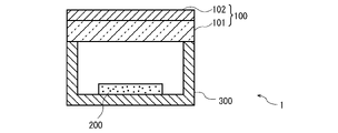
- FIG. 1 is a diagram illustrating a configuration of a near-infrared cut filter according to a first embodiment of the present invention.
- FIG. 2 is a vertical cross-sectional view illustrating the configuration of an image pickup apparatus equipped with a near-infrared cut filter according to the first embodiment of the present invention.
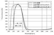
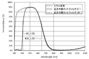
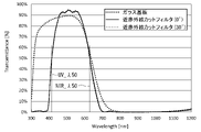
- FIG. 3 is a diagram showing a spectral transmittance curve of a near-infrared cut filter according to the first embodiment (Example 1) of the present invention and a glass substrate used in the near-infrared cut filter.
- FIG. 1 is a diagram illustrating a configuration of a near-infrared cut filter according to a first embodiment of the present invention.
- FIG. 2 is a vertical cross-sectional view illustrating the configuration of an image pickup apparatus equipped with a near-infrared cut filter according to the first embodiment of the present invention.
- FIG. 3 is a diagram showing a spectral transmittance curve of a near-infrared cut filter according to the
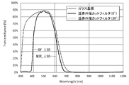
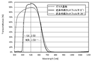
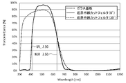
- FIG. 4 is a diagram showing a spectral transmittance curve of a near-infrared cut filter according to the first embodiment (Example 2) of the present invention and a glass substrate used in the near-infrared cut filter.
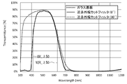
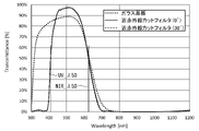
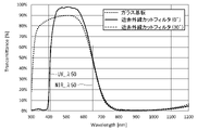
- FIG. 5 is a diagram showing a spectral transmittance curve of a near-infrared cut filter according to a first embodiment (Example 3) of the present invention and a glass substrate used in the near-infrared cut filter.
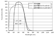
- FIG. 6 is a diagram showing a spectral transmittance curve of a near-infrared cut filter according to a first embodiment (Example 4) of the present invention and a glass substrate used in the near-infrared cut filter.
- FIG. 5 is a diagram showing a spectral transmittance curve of a near-infrared cut filter according to a first embodiment (Example 3) of the present invention and a glass substrate used in the near-infrared cut filter.
- FIG. 6 is
- FIG. 7 is a diagram showing a spectral transmittance curve of a near-infrared cut filter according to a first embodiment (Example 5) of the present invention and a glass substrate used in the near-infrared cut filter.
- FIG. 8 is a diagram showing a spectral transmittance curve of a near-infrared cut filter according to the first embodiment (Example 6) of the present invention and a glass substrate used in the near-infrared cut filter.
- FIG. 9 is a diagram showing a spectral transmittance curve of a near-infrared cut filter according to a first embodiment (Example 7) of the present invention and a glass substrate used in the near-infrared cut filter.
- FIG. 10 is a diagram showing a spectral transmittance curve of a near-infrared cut filter according to the first embodiment (Example 8) of the present invention and a glass substrate used in the near-infrared cut filter.
- FIG. 11 is a diagram showing a spectral transmittance curve of a near-infrared cut filter according to a first embodiment (Example 9) of the present invention and a glass substrate used in the near-infrared cut filter.
- FIG. 12 is a diagram showing a spectral transmittance curve of a near-infrared cut filter according to a first embodiment (Example 10) of the present invention and a glass substrate used in the near-infrared cut filter.
- FIG. 10 is a diagram showing a spectral transmittance curve of a near-infrared cut filter according to the first embodiment (Example 8) of the present invention and a glass substrate used in the near-infrared cut filter.
- FIG. 13 is a diagram showing a spectral transmittance curve of a near-infrared cut filter according to the first embodiment (Example 11) of the present invention and a glass substrate used in the near-infrared cut filter.
- FIG. 14 is a vertical cross-sectional view illustrating the configuration of the near-infrared cut filter according to the second embodiment of the present invention.
- FIG. 15 is a diagram showing a spectral transmittance curve of the near-infrared cut filter according to the second embodiment (Example 12) of the present invention.
- FIG. 16 is a diagram showing a spectral transmittance curve of the near-infrared cut filter according to the second embodiment (Example 13) of the present invention.
- FIG. 17 is a diagram showing a spectral transmittance curve of the near-infrared cut filter according to the second embodiment (Example 14) of the present invention.
- FIG. 18 is a diagram showing a spectral transmittance curve of the near-infrared cut filter according to the second embodiment (Example 15) of the present invention.
- FIG. 19 is a diagram showing a spectral transmittance curve of the near-infrared cut filter according to the second embodiment (Example 16) of the present invention.
- FIG. 20 is a diagram showing a spectral transmittance curve of the near-infrared cut filter according to the second embodiment (Example 17) of the present invention.
- FIG. 18 is a diagram showing a spectral transmittance curve of the near-infrared cut filter according to the second embodiment (Example 15) of the present invention.
- FIG. 19 is a diagram showing a spectral transmittance curve of the near-infrared cut filter according to
- FIG. 21 is a diagram showing a spectral transmittance curve of the near-infrared cut filter according to the second embodiment (Example 18) of the present invention.
- FIG. 22 is a diagram showing a spectral transmittance curve of the near-infrared cut filter according to the second embodiment (Example 19) of the present invention.
- FIG. 23 is a diagram showing a spectral transmittance curve of the near-infrared cut filter according to the second embodiment (Example 20) of the present invention.
- FIG. 24 is a diagram showing a spectral transmittance curve of the near-infrared cut filter according to the second embodiment (Example 21) of the present invention.
- FIG. 25 is a diagram showing a spectral transmittance curve of the near-infrared cut filter according to the second embodiment (Example 22) of the present invention.
- FIG. 26 is a vertical cross-sectional view illustrating the configuration of the near-infrared cut filter according to the third embodiment (Example 23) of the present invention.
- FIG. 27 is a vertical cross-sectional view illustrating the configuration of the near-infrared cut filter according to the third embodiment (Example 24) of the present invention.
- FIG. 28 is a vertical cross-sectional view illustrating the configuration of the near-infrared cut filter according to the third embodiment (Example 25) of the present invention.
- FIG. 26 is a vertical cross-sectional view illustrating the configuration of the near-infrared cut filter according to the third embodiment (Example 23) of the present invention.
- FIG. 27 is a vertical cross-sectional view illustrating the configuration of the near-infrared cut filter according to the third embodiment (Ex
- FIG. 29 is a vertical cross-sectional view showing the configuration of a conventional near-infrared cut filter.
- FIG. 30 is a diagram showing a spectral transmittance curve of a reflective layer used in a conventional near-infrared cut filter.
- FIG. 31 is a diagram showing a spectral transmittance curve of a conventional near-infrared cut filter.
- FIGS. 1A and 1B are views for explaining the configuration of the near-infrared cut filter 100 according to the first embodiment of the present invention
- FIG. 1A is a plan view
- FIG. 1B is a vertical sectional view. be.
- FIG. 2 is a vertical cross-sectional view illustrating the configuration of the image pickup apparatus 1 in which the opening of the package 300 of the solid-state image pickup device 200 is sealed by the near-infrared cut filter 100 of the present embodiment.
- the near-infrared cut filter 100 of the present embodiment is attached to the front surface of the package 300 that houses the solid-state image sensor 200 to protect the solid-state image sensor 200 and the solid-state image sensor 200. It is an optical element used for visual sensitivity correction.
- the near-infrared cut filter 100 of the present embodiment has a rectangular plate shape (for example, 6 mm (horizontal direction) ⁇ 5 mm (longitudinal direction)), and has a glass base material 101 (transparent group). The material) and the resin layer 102 formed on one main surface of the glass base material 101 (the upper surface in FIG. 1B).
- the glass base material 101 of the present embodiment is, for example, an absorbent glass substrate made of phosphate-based glass or fluoride-based glass.
- the thickness of the glass base material 101 of the present embodiment is preferably 0.35 mm or less, more preferably 0.16 to 0.26 mm, from the viewpoint of reducing the size and weight.
- the phosphate-based glass in the present embodiment is a glass containing P and O as essential components and other optional components, and a glass containing CuO is particularly preferable. Since the phosphate-based glass contains CuO, near-infrared light can be absorbed more effectively. Examples of other optional components of the phosphate-based glass include Ca, Mg, Sr, Ba, Li, Na, K, and Cs.
- P 2 O 5 Exceeding 0% by mass and 80% by mass or less, Al 2 O 3 : 0-40% by mass, BaO: 0-40% by mass, CuO: 0-40% by mass Is preferable.
- the fluorinated glass in the present embodiment is a glass containing P, O, F as essential components and other optional components, and a glass containing CuO is particularly preferable. Since the futurate-based glass contains CuO, near-infrared light can be absorbed more effectively.
- Other optional components of the fluorinated glass include, for example, Ca, Mg, Sr, Ba, Li, Na, K, Cs and the like.
- one containing BaO is preferably used.
- the devitrification resistance and meltability of the glass can be improved. If it is more than 10%, devitrification is likely to occur, so 0 to 10% is preferable.
- the BaO content is more preferably 1 to 10% and even more preferably 1 to 5%.
- those containing Al 2 O 3 are preferably used.
- the stability and chemical durability of the glass can be improved. If it is more than 10%, devitrification is likely to occur, so 0 to 10% is preferable.
- the content of Al 2 O 3 is more preferably 1 to 10%, further preferably 1 to 5%.
- one containing Y 2 O 3 is preferably used.
- the refractive index can be increased while maintaining thermal stability. If it is more than 10%, devitrification is likely to occur, and the glass transition temperature and the yield point temperature rise. Therefore, 0 to 10% is preferable.
- the content of Y 2 O 3 is more preferably 1 to 10%, further preferably 1 to 5%.
- one containing BaCl 2 is preferably used as the futurate-based glass.
- the difference between the crystallization start temperature (Tx) and the glass transition temperature (Tg) of the glass becomes large, and the stability of the glass against devitrification is improved. If it is more than 10%, devitrification is likely to occur, so 0 to 10% is preferable.
- the content of BaCl 2 is more preferably 1 to 10%, further preferably 1 to 5%.
- fluoride-based glass P 2 O 5 : Exceeding 0% by mass and 70% by mass or less, Al 2 O 3 : 0-40% by mass, BaO: 0-40% by mass, CuO: 0-40% by mass , And further contains fluoride in an amount of more than 0% by mass and 40% by mass or less.
- P 2 O 5 20 to 60% by mass
- Al 2 O 3 0 to 10% by mass
- BaO 0-10% by mass
- CuO 0 to 10% by mass
- P 2 O 5 20 to 60% by mass
- Al 2 O 3 0 to 10% by mass
- BaO 0-10% by mass
- CuO 0 to 10% by mass
- P 2 O 5 20 to 60% by mass
- Al 2 O 3 1 to 10% by mass
- BaO 1-10% by mass
- CuO 1-10% by mass
- Examples of the fluoride include one or more selected from MgF 2 , CaF 2 , SrF 2 , and the like.
- P 2 O 5 40 to 50% by mass
- Al 2 O 3 1 to 10% by mass
- BaO 1-10% by mass
- CuO 1-10% by mass
- MgF 2 1 to 10% by mass
- CaF 2 1 to 10% by mass
- SrF 2 1 to 10% by mass
- Y 2 O 3 1 to 10% by mass
- BaCl 2 0 to 1% by mass
- the glass substrate 101 of the present embodiment is preferably configured so that the average transmittance in the wavelength range of 800 to 1100 nm is 3% or less, and further preferably 1% or less. preferable.
- the glass base material 101 having a small average transmittance in the wavelength range of 800 to 1100 nm is used, visible light is used without using the reflective film (dielectric multilayer film) used in the conventional near-infrared cut filter.
- a cut filter that selectively transmits light in a region can be manufactured.
- the glass substrate 101 preferably has an average transmittance of 15% or less, more preferably 10% or less, and further preferably 8% or less in the wavelength range of 720 to 750 nm. Further, the glass substrate 101 preferably has an average transmittance of 40% or less, more preferably 10% or less, and further preferably 8% or less in the wavelength range of 650 to 720 nm. Further, the glass substrate 101 preferably has an average transmittance of 5% or less, more preferably 3% or less, and further preferably 2% or less in the wavelength range of 800 to 1200 nm.
- the glass substrate 101 preferably has a half-wavelength (UV_ ⁇ 50) on the short wavelength side of the transmittance curve in the range of 300 to 400 nm, more preferably in the range of 305 to 350 nm, and preferably in the range of 310 to 340 nm. It is more preferable to be in. Further, the glass substrate 101 preferably has a half-value wavelength (NIR_ ⁇ 50) on the long wavelength side of the transmittance curve in the range of 590 to 670 nm, and more preferably in the range of 610 to 650 nm.
- UV_ ⁇ 50 half-wavelength
- NIR_ ⁇ 50 half-value wavelength
- the half-value wavelength means the wavelength when the transmittance becomes 50%
- the half-value wavelength (UV_ ⁇ 50) on the short wavelength side means the transmittance becomes 50% at the rising edge of the transmittance curve
- the half-value wavelength (NIR_ ⁇ 50) on the long wavelength side refers to the wavelength at which the transmittance becomes 50% at the falling edge of the transmittance curve.
- the resin layer 102 of the present embodiment is a layer composed of a dye and a resin that absorb light of a specific wavelength.
- the resin layer 102 contains, for example, at least one of a near-infrared absorbing dye and an ultraviolet absorbing dye and a transparent resin, and it is preferable that the dye is uniformly dissolved or dispersed in the transparent resin. Further, it is preferable that the resin layer 102 of the present embodiment contains a Si atom as an essential component and at least one selected from a Ti atom, a Zr atom and an Al atom as an optional component.
- the near-infrared absorbing dye constituting the resin layer 102 conventionally known dyes can be adopted, for example, cyanine-based dyes, polymethine-based dyes, squarylium-based dyes, porphyrin-based dyes, metal dithiol complex-based dyes, and phthalocyanine-based dyes.
- cyanine-based dyes polymethine-based dyes, squarylium-based dyes, porphyrin-based dyes, metal dithiol complex-based dyes, and phthalocyanine-based dyes.
- One or more selected from dyes, diimonium pigments and inorganic oxide particles can be used, and one or more selected from squarylium pigments, cyanine pigments and phthalocyanine pigments are more preferable.
- dyes can be used as the ultraviolet absorbing dye constituting the resin layer 102.
- benzotriazole-based compounds benzophenone-based compounds, triazine-based compounds, styryl-based compounds, benzoxazine-based compounds, and cyanoacrylates can be used.
- One or more selected from systems, oxanilide compounds, salicylate compounds, formamidine compounds, indole compounds, and azomethine compounds can be used, and benzotriazole compounds, benzophenone compounds, triazine compounds, and styryl compounds can be used. More preferably, one or more selected from the compounds.
- the resin constituting the resin layer 102 a conventionally known transparent resin can be adopted, and acrylic resin, epoxy resin, en-thiol resin, polycarbonate resin, polyether resin, polyarylate resin, polysulfone resin, and polyether monkey can be adopted. Examples thereof include one or more selected from phon resin, polyparaphenylene resin, polyarylene ether phosphine oxide resin, polyimide resin, polyamideimide resin, polyolefin resin, cyclic olefin resin and polyester resin.
- a resin having a high glass transition point (Tg) is preferable from the viewpoint of transparency, solubility of the near-infrared absorbing dye in the transparent resin, and heat resistance, and therefore a thermosetting resin is preferable.
- polyester resin polycarbonate resin, polyether sulfone resin, polyarylate resin, polyimide resin, and epoxy resin
- polyester resin one or more selected from polyethylene terephthalate resin and polyethylene naphthalate resin are preferable.
- thermoplastic resin can be suitably used as a transparent resin by increasing the heat resistance by adjusting a functional group or the like.
- acrylic resins, polyamide resins, polyolefin resins and the like, which can increase heat resistance by adjusting functional groups and the like, can also be used as the transparent resin.
- the resin layer 102 further includes a color correction dye, a leveling agent, an antioxidant, a heat stabilizer, a light stabilizer, and an antioxidant as long as the effects of the present invention are not impaired.
- a color correction dye e.g., a leveling agent, an antioxidant, a heat stabilizer, a light stabilizer, and an antioxidant as long as the effects of the present invention are not impaired.
- Dispersant, flame retardant, lubricant, plasticizer and other optional components may be contained.
- a dye, a transparent resin, and an optional compounding component are dissolved or dispersed in a solvent to prepare a resin film-forming liquid, which is coated, dried, and further cured if necessary.
- a resin film-forming liquid may contain a known surfactant such as a cationic type, an anion type, or a nonionic type.
- one or more coating methods selected from the immersion coating method, the cast coating method, the spray coating method, the spin coating method and the like can be adopted.
- the resin layer 102 is a layer formed on the glass base material 101 and configured to absorb light having a specific wavelength, and the absorption wavelength is set according to the spectral transmittance characteristics of the glass base material 101. By setting (that is, selecting the optimum dye), light in a desired visible light region can be extracted.
- the resin layer 102 of the present embodiment employs an ultraviolet absorbing dye having a maximum absorption wavelength of 340 to 400 nm and a near infrared absorbing dye having a maximum absorption wavelength of 650 to 900 nm. can do.
- the resin layer 102 of the present embodiment is formed on one main surface of the glass base material 101 (the upper surface in FIG. 1B), but is not limited to such a configuration. ..
- the resin layer 102 may be formed on the other main surface of the glass base material 101 (the lower surface in FIG. 1B), or may be formed on both sides of the glass base material 101. Further, the resin layer 102 does not necessarily have to be one layer, and may be composed of a plurality of layers.
- the spectral transmittance curve of the near-infrared cut filter 100 on which the resin layer 102 is formed has a half-wavelength (UV_ ⁇ 50) on the short wavelength side of the transmittance curve of 385 to 430 nm and a half-wavelength (NIR_ ⁇ 50) on the long wavelength side. ) Is 3.0% or less in the wavelength range of 590 to 660 nm and 800 to 1100 nm, which is a characteristic close to human visual sensitivity (details will be described later).
- the near-infrared cut filter 100 of the present embodiment is attached to the front surface of the solid-state imaging element 200, the half-wavelength on the short wavelength side of the transmittance curve is viewed from the viewpoint of the amount of light incident on the solid-state imaging element 200. It is preferable that the difference between (UV_ ⁇ 50) and the half-value wavelength (NIR_ ⁇ 50) on the long wavelength side is large, and in particular, the one having a long half-value wavelength (NIR_ ⁇ 50) on the long wavelength side within the range of human luminosity factor is preferable.
- the half-wavelength (NIR_ ⁇ 50) on the long wavelength side of the transmittance curve of the near-infrared cut filter 100 is close to the half-wavelength (NIR_ ⁇ 50) on the long wavelength side of the transmittance curve of the glass substrate 101. Is set to. More specifically, in the present embodiment, the half-wavelength (NIR_ ⁇ 50) on the long wavelength side of the transmittance curve of the glass substrate 101 and the half-wavelength (NIR_ ⁇ 50) on the long wavelength side of the transmittance curve of the near-infrared cut filter 100.
- the difference from the above is configured to be 20 nm or less.
- the difference between the two is more preferably 15 nm or less, and further preferably 10 nm or less.
- the image pickup device 1 includes a solid-state image sensor 200, a package 300 for accommodating the solid-state image sensor 200, and a near-infrared cut filter 100 attached to the front surface of the package 300. ..
- Examples of the solid-state image sensor 200 include image sensors such as CCD (Charge-Coupled Device) and CMOS (Complementary Metal Oxide Semiconductor).
- image sensors such as CCD (Charge-Coupled Device) and CMOS (Complementary Metal Oxide Semiconductor).
- the solid-state image sensor 200 is arranged at substantially the center of the bottom surface of the box-shaped package 300 so that the other main surface side (lower side in FIG. 1B) of the near-infrared cut filter 100 faces the solid-state image sensor 200. Is attached to the opening of the package 300.
- the resin layer 102 side of the near-infrared cut filter 100 is an incident surface on which light directed toward the solid-state image sensor 200 is incident, and the other main surface side of the near-infrared cut filter 100 is an exit surface.
- the configuration is not necessarily limited to this, and the near-infrared cut filter 100 may be mounted upside down (that is, the resin layer 102 faces the solid-state image sensor 200).
- the near-infrared cut filter 100 is attached to the opening of the package 300 and has a configuration that also serves as a so-called cover glass, but the configuration is not necessarily limited to such a configuration. ..
- the image pickup device 1 may include a lens group (not shown) that guides light to the solid-state image pickup device 200.
- the near-infrared cut filter 100 may be arranged closer to the image pickup apparatus 1 than the lens group, and a cover glass may be provided further closer to the image pickup apparatus 1 than the near-infrared ray cut filter 100.
- the near-infrared cut filter 100 of the present embodiment will be further described with reference to Examples and Comparative Examples, but the present invention is not limited to the following Examples.
- FIG. 3 is a diagram showing a spectral transmittance curve (dotted line) of the glass substrate 101 of Example 1 and a spectral transmittance curve (solid line, broken line) of the near-infrared cut filter 100 of Example 1.
- the vertical axis of FIG. 3 is the transmittance (%), and the horizontal axis is the wavelength (nm).
- the spectral transmittance curve of the near-infrared cut filter 100 shows a spectral transmittance curve (solid line) when the incident angle is 0 ° and a spectral transmittance curve (broken line) when the incident angle is 30 °.
- the glass substrate 101 of this example has an average transmittance of 0.34% (that is, 1% or less) in the wavelength range of 800 to 1100 nm. Further, the glass substrate 101 of this example has an average transmittance of 0.62% (that is, 15% or less) in the wavelength range of 720 to 750 nm. Further, the glass base material 101 has an average transmittance of 5.3% (that is, 40% or less) in the wavelength range of 650 to 720 nm.
- the glass base material 101 has an average transmittance of 0.93% (that is, 5% or less) in the wavelength range of 800 to 1200 nm.
- the half-value wavelength (UV_ ⁇ 50) on the short wavelength side of the transmittance curve is about 350 nm (that is, within the range of 300 to 400 nm), and the half-value wavelength (NIR_ ⁇ 50) on the long wavelength side. Is about 599 nm (that is, in the range of 590 to 670 nm).
- resin layer 102 Acrylic resin (transparent resin), styryl compound and triazine compound (ultraviolet absorbing dye), and squarylium compound (near infrared absorbing dye) are mixed in a container at a predetermined mixing ratio to prepare a resin film forming liquid. Then, the obtained resin film-forming liquid was applied onto the glass substrate 101 using a spin coater. Then, the glass base material 101 coated with the resin film forming liquid was placed on a hot plate heated to 160 ° C. and heated for 20 minutes to be cured, thereby producing the near-infrared cut filter 100 of the present embodiment.
- the spectral transmittance curve (solid line, broken line) of the near-infrared cut filter 100 of this embodiment has a half-value wavelength (UV_ ⁇ 50) on the short wavelength side of the transmittance curve of about 413 nm and a half-value on the long wavelength side.
- the average transmittance in the wavelength range of about 591 nm and 800 to 1100 nm was 0.34%, and the characteristics close to human visual sensitivity were obtained.
- the difference between the half-wavelength (NIR_ ⁇ 50) on the long wavelength side of the transmittance curve of the glass substrate 101 and the half-wavelength (NIR_ ⁇ 50) on the long wavelength side of the transmittance curve of the near-infrared cut filter 100 is , 8 nm.
- the near-infrared cut filter 100 of this embodiment does not have a reflective film like the conventional near-infrared cut filter, the performance as a cut filter is remarkably improved even when light having an incident angle of 30 ° is incident. The generation of impaired phase shift, wavelength shift and ripple is suppressed.
- Example 2 For the near-infrared cut filter 100 of Example 2, a fluorium-based compound (CXD700) manufactured by HOYA Corporation having a thickness of 0.3 mm was selected as the glass base material 101, and the squarylium-based compound of the resin layer 102 ( It differs from Example 1 in that the content of the near-infrared absorbing dye) is changed.
- CXD700 fluorium-based compound manufactured by HOYA Corporation having a thickness of 0.3 mm
- FIG. 4 is a diagram showing a spectral transmittance curve (dotted line) of the glass substrate 101 of Example 2 and a spectral transmittance curve (solid line, broken line) of the near-infrared cut filter 100 of Example 2.
- a spectral transmittance curve (solid line) when the incident angle is 0 ° and a spectral transmittance curve (broken line) when the incident angle is 30 ° are shown.
- the glass substrate 101 of this example has an average transmittance of 0.71% or less (that is, 1% or less) in the wavelength range of 800 to 1100 nm. Further, the glass substrate 101 of this example has an average transmittance of 1.26% (that is, 15% or less) in the wavelength range of 720 to 750 nm. Further, the glass base material 101 has an average transmittance of 7.7% (that is, 40% or less) in the wavelength range of 650 to 720 nm. Further, the glass base material 101 has an average transmittance of 1.65% (that is, 5% or less) in the wavelength range of 800 to 1200 nm.
- the half-value wavelength (UV_ ⁇ 50) on the short wavelength side of the transmittance curve is about 348 nm (that is, within the range of 300 to 400 nm), and the half-value wavelength (NIR_ ⁇ 50) on the long wavelength side. Is about 604 nm (that is, in the range of 590 to 670 nm).
- the near-infrared cut filter 100 of this embodiment has a half-wavelength (UV_ ⁇ 50) on the short wavelength side of the transmittance curve of about 411 nm and a half-wavelength (NIR_ ⁇ 50) on the long wavelength side of about 600 nm, in the wavelength range of 800 to 1100 nm.
- the average transmittance was 0.71% or less, and a characteristic close to human visual sensitivity was obtained.
- the difference between the half-wavelength (NIR_ ⁇ 50) on the long wavelength side of the transmittance curve of the glass substrate 101 and the half-wavelength (NIR_ ⁇ 50) on the long wavelength side of the transmittance curve of the near-infrared cut filter 100 is It became 4 nm.
- the near-infrared cut filter 100 of this embodiment does not have a reflective film like the conventional near-infrared cut filter, the performance as a cut filter is remarkably improved even when light having an incident angle of 30 ° is incident. The generation of impaired phase shift, wavelength shift and ripple is suppressed.
- the near-infrared cut filter 100 of Example 3 is a phosphate-based glass having a thickness of 0.30 mm newly developed by HOYA Co., Ltd. as a glass base material 101. Filing date: July 10, 2nd year of Reiwa))))), the resin layer 102 is made of acrylic resin (transparent resin), styryl compound and triazine compound (ultraviolet absorbing dye), squarylium compound and cyanine. It differs from Example 1 in that it is formed by a compound (near-infrared absorbing dye) (that is, the type of the near-infrared absorbing dye is changed).
- FIG. 5 is a diagram showing a spectral transmittance curve (dotted line) of the glass substrate 101 of Example 3 and a spectral transmittance curve (solid line, broken line) of the near-infrared cut filter 100 of Example 3.
- a spectral transmittance curve (solid line) when the incident angle is 0 ° and a spectral transmittance curve (broken line) when the incident angle is 30 ° are shown.
- the glass substrate 101 of this example has an average transmittance of 0.03% (that is, 1% or less) in the wavelength range of 800 to 1100 nm. Further, the glass substrate 101 of this example has an average transmittance of 1.03% (that is, 15% or less) in the wavelength range of 720 to 750 nm. Further, the glass base material 101 has an average transmittance of 11.1% (that is, 40% or less) in the wavelength range of 650 to 720 nm. Further, the glass base material 101 has an average transmittance of 0.11% (that is, 5% or less) in the wavelength range of 800 to 1200 nm.
- the half-value wavelength (UV_ ⁇ 50) on the short wavelength side of the transmittance curve is about 319 nm (that is, within the range of 300 to 400 nm), and the half-value wavelength (NIR_ ⁇ 50) on the long wavelength side. Is about 622 nm (that is, in the range of 590 to 670 nm).
- the near-infrared cut filter 100 of this embodiment has a half-wavelength (UV_ ⁇ 50) on the short wavelength side of the transmittance curve of about 413 nm and a half-wavelength (NIR_ ⁇ 50) on the long wavelength side of about 610 nm, in the wavelength range of 800 to 1100 nm.
- the average transmittance was 0.03%, and a characteristic close to human visual sensitivity was obtained.
- the difference between the half-wavelength (NIR_ ⁇ 50) on the long wavelength side of the transmittance curve of the glass substrate 101 and the half-wavelength (NIR_ ⁇ 50) on the long wavelength side of the transmittance curve of the near-infrared cut filter 100 is , 12 nm.
- the near-infrared cut filter 100 of this embodiment does not have a reflective film like the conventional near-infrared cut filter, the performance as a cut filter is remarkably improved even when light having an incident angle of 30 ° is incident. The generation of impaired phase shift, wavelength shift and ripple is suppressed.
- Example 4 The near-infrared cut filter 100 of Example 4 was carried out at the point that a glass base material 101 having a thickness of 0.26 mm was selected and the type and content of the near-infrared absorbing dye of the resin layer 102 were changed. It is different from Example 3.
- FIG. 6 is a diagram showing a spectral transmittance curve (dotted line) of the glass substrate 101 of Example 4 and a spectral transmittance curve (solid line, broken line) of the near-infrared cut filter 100 of Example 4.
- a spectral transmittance curve (solid line) when the incident angle is 0 ° and a spectral transmittance curve (broken line) when the incident angle is 30 ° are shown.
- the glass substrate 101 of this example has an average transmittance of 0.09% (that is, 1% or less) in the wavelength range of 800 to 1100 nm. Further, the glass substrate 101 of this example has an average transmittance of 1.85% (that is, 15% or less) in the wavelength range of 720 to 750 nm. Further, the glass substrate 101 has an average transmittance of 14.3% (that is, 40% or less) in the wavelength range of 650 to 720 nm. Further, the glass substrate 101 has an average transmittance of 0.25% (that is, 5% or less) in the wavelength range of 800 to 1200 nm.
- the half-value wavelength (UV_ ⁇ 50) on the short wavelength side of the transmittance curve is about 317 nm (that is, within the range of 300 to 400 nm), and the half-value wavelength (NIR_ ⁇ 50) on the long wavelength side. Is about 628 nm (that is, in the range of 590 to 670 nm).
- the near-infrared cut filter 100 of this embodiment has a half-wavelength (UV_ ⁇ 50) on the short wavelength side of the transmittance curve of about 411 nm and a half-wavelength (NIR_ ⁇ 50) on the long wavelength side of about 619 nm, in the wavelength range of 800 to 1100 nm.
- the average transmittance was 0.08%, and a characteristic close to human visual sensitivity was obtained.
- the difference between the half-wavelength (NIR_ ⁇ 50) on the long wavelength side of the transmittance curve of the glass substrate 101 and the half-wavelength (NIR_ ⁇ 50) on the long wavelength side of the transmittance curve of the near-infrared cut filter 100 is , 9 nm.
- the near-infrared cut filter 100 of this embodiment does not have a reflective film like the conventional near-infrared cut filter, the performance as a cut filter is remarkably improved even when light having an incident angle of 30 ° is incident. The generation of impaired phase shift, wavelength shift and ripple is suppressed.
- Example 5 The near-infrared cut filter 100 of Example 5 was carried out at the point that a glass base material 101 having a thickness of 0.25 mm was selected and the type and content of the near-infrared absorbing dye of the resin layer 102 were changed. It is different from Example 3.
- FIG. 7 is a diagram showing a spectral transmittance curve (dotted line) of the glass substrate 101 of Example 5 and a spectral transmittance curve (solid line, broken line) of the near-infrared cut filter 100 of Example 5.
- a spectral transmittance curve (solid line) when the incident angle is 0 ° and a spectral transmittance curve (broken line) when the incident angle is 30 ° are shown.
- the glass substrate 101 of this example has an average transmittance of 0.11% (that is, 1% or less) in the wavelength range of 800 to 1100 nm. Further, the glass substrate 101 of this example has an average transmittance of 2.15% (that is, 15% or less) in the wavelength range of 720 to 750 nm. Further, the glass base material 101 has an average transmittance of 15.3% (that is, 40% or less) in the wavelength range of 650 to 720 nm. Further, the glass substrate 101 has an average transmittance of 0.31% (that is, 5% or less) in the wavelength range of 800 to 1200 nm.
- the half-value wavelength (UV_ ⁇ 50) on the short wavelength side of the transmittance curve is about 316 nm (that is, within the range of 300 to 400 nm), and the half-value wavelength (NIR_ ⁇ 50) on the long wavelength side. Is about 629 nm (that is, in the range of 590 to 670 nm).
- the near-infrared cut filter 100 of this embodiment has a half-wavelength (UV_ ⁇ 50) on the short wavelength side of the transmittance curve of about 411 nm and a half-wavelength (NIR_ ⁇ 50) on the long wavelength side of about 620 nm, in the wavelength range of 800 to 1100 nm.
- the average transmittance was 0.31%, and a characteristic close to human visual sensitivity was obtained.
- the difference between the half-wavelength (NIR_ ⁇ 50) on the long wavelength side of the transmittance curve of the glass substrate 101 and the half-wavelength (NIR_ ⁇ 50) on the long wavelength side of the transmittance curve of the near-infrared cut filter 100 is , 9 nm.
- the near-infrared cut filter 100 of this embodiment does not have a reflective film like the conventional near-infrared cut filter, the performance as a cut filter is remarkably improved even when light having an incident angle of 30 ° is incident. The generation of impaired phase shift, wavelength shift and ripple is suppressed.
- Example 6 The near-infrared cut filter 100 of Example 6 was carried out at the point that a glass base material 101 having a thickness of 0.227 mm was selected and the type and content of the near-infrared absorbing dye of the resin layer 102 were changed. It is different from Example 3.
- FIG. 8 is a diagram showing a spectral transmittance curve (dotted line) of the glass substrate 101 of Example 6 and a spectral transmittance curve (solid line, broken line) of the near-infrared cut filter 100 of Example 6.
- a spectral transmittance curve (solid line) when the incident angle is 0 ° and a spectral transmittance curve (broken line) when the incident angle is 30 ° are shown.
- the glass substrate 101 of this example has an average transmittance of 0.20% (that is, 1% or less) in the wavelength range of 800 to 1100 nm. Further, the glass base material 101 of this example has an average transmittance of 3.02% (that is, 15% or less) in the wavelength range of 720 to 750 nm. Further, the glass base material 101 has an average transmittance of 17.7% (that is, 40% or less) in the wavelength range of 650 to 720 nm. Further, the glass base material 101 has an average transmittance of 0.49% (that is, 5% or less) in the wavelength range of 800 to 1200 nm.
- the half-value wavelength (UV_ ⁇ 50) on the short wavelength side of the transmittance curve is about 315 nm (that is, within the range of 300 to 400 nm), and the half-value wavelength (NIR_ ⁇ 50) on the long wavelength side. Is about 633 nm (that is, in the range of 590 to 670 nm).
- the near-infrared cut filter 100 of this embodiment has a half-wavelength (UV_ ⁇ 50) on the short wavelength side of the transmittance curve of about 411 nm and a half-wavelength (NIR_ ⁇ 50) on the long wavelength side of about 625 nm, in the wavelength range of 800 to 1100 nm.
- the average transmittance was 0.20%, and a characteristic close to human visual sensitivity was obtained.
- the difference between the half-wavelength (NIR_ ⁇ 50) on the long wavelength side of the transmittance curve of the glass substrate 101 and the half-wavelength (NIR_ ⁇ 50) on the long wavelength side of the transmittance curve of the near-infrared cut filter 100 is , 8 nm.
- the near-infrared cut filter 100 of this embodiment does not have a reflective film like the conventional near-infrared cut filter, the performance as a cut filter is remarkably improved even when light having an incident angle of 30 ° is incident. The generation of impaired phase shift, wavelength shift and ripple is suppressed.
- Example 7 The near-infrared cut filter 100 of Example 7 was selected as the glass base material 101 having a thickness of 0.210 mm, and the type of the near-infrared absorbing dye of the resin layer 102 was only a squarylium compound. It is different from Example 3.
- FIG. 9 is a diagram showing a spectral transmittance curve (dotted line) of the glass substrate 101 of Example 7 and a spectral transmittance curve (solid line, broken line) of the near-infrared cut filter 100 of Example 7.
- a spectral transmittance curve (solid line) when the incident angle is 0 ° and a spectral transmittance curve (broken line) when the incident angle is 30 ° are shown.
- the glass substrate 101 of this example has an average transmittance of 0.31% (that is, 1% or less) in the wavelength range of 800 to 1100 nm. Further, the glass substrate 101 of this example has an average transmittance of 3.88% (that is, 15% or less) in the wavelength range of 720 to 750 nm. Further, the glass substrate 101 has an average transmittance of 19.9% (that is, 40% or less) in the wavelength range of 650 to 720 nm. Further, the glass base material 101 has an average transmittance of 0.70% (that is, 5% or less) in the wavelength range of 800 to 1200 nm.
- the half-value wavelength (UV_ ⁇ 50) on the short wavelength side of the transmittance curve is about 314 nm (that is, within the range of 300 to 400 nm), and the half-value wavelength (NIR_ ⁇ 50) on the long wavelength side. Is about 636 nm (that is, in the range of 590 to 670 nm).
- the near-infrared cut filter 100 of this embodiment has a half-wavelength (UV_ ⁇ 50) on the short wavelength side of the transmittance curve of about 418 nm and a half-wavelength (NIR_ ⁇ 50) on the long wavelength side of about 625 nm, in the wavelength range of 800 to 1100 nm.
- the average transmittance was 0.27%, and a characteristic close to human visual sensitivity was obtained.
- the difference between the half-wavelength (NIR_ ⁇ 50) on the long wavelength side of the transmittance curve of the glass substrate 101 and the half-wavelength (NIR_ ⁇ 50) on the long wavelength side of the transmittance curve of the near-infrared cut filter 100 is , 11 nm.
- the near-infrared cut filter 100 of this embodiment does not have a reflective film like the conventional near-infrared cut filter, the performance as a cut filter is remarkably improved even when light having an incident angle of 30 ° is incident. The generation of impaired phase shift, wavelength shift and ripple is suppressed.
- Example 8 The near-infrared cut filter 100 of Example 8 is different from Example 7 in that the content of the near-infrared absorbing dye in the resin layer 102 is changed.
- FIG. 10 is a diagram showing a spectral transmittance curve (dotted line) of the glass substrate 101 of Example 8 and a spectral transmittance curve (solid line, broken line) of the near-infrared cut filter 100 of Example 8.
- a spectral transmittance curve (solid line) when the incident angle is 0 ° and a spectral transmittance curve (broken line) when the incident angle is 30 ° are shown.
- the near-infrared cut filter 100 of this embodiment has a half-wavelength (UV_ ⁇ 50) on the short wavelength side of the transmittance curve of about 412 nm and a half-wavelength (NIR_ ⁇ 50) on the long wavelength side of about 630 nm, 800 to
- the average transmittance in the wavelength range of 1100 nm was 0.29%, and a characteristic close to human visual sensitivity was obtained.
- the difference between the half-wavelength (NIR_ ⁇ 50) on the long wavelength side of the transmittance curve of the glass substrate 101 and the half-wavelength (NIR_ ⁇ 50) on the long wavelength side of the transmittance curve of the near-infrared cut filter 100 is , 6 nm.
- the near-infrared cut filter 100 of this embodiment does not have a reflective film like the conventional near-infrared cut filter, the performance as a cut filter is remarkably improved even when light having an incident angle of 30 ° is incident. The generation of impaired phase shift, wavelength shift and ripple is suppressed.
- Example 9 The near-infrared cut filter 100 of Example 9 was carried out at the point that a glass base material 101 having a thickness of 0.165 mm was selected and the type and content of the near-infrared absorbing dye of the resin layer 102 were changed. It is different from Example 8.
- FIG. 11 is a diagram showing a spectral transmittance curve (dotted line) of the glass substrate 101 of Example 9 and a spectral transmittance curve (solid line, broken line) of the near-infrared cut filter 100 of Example 9.
- a spectral transmittance curve (solid line) when the incident angle is 0 ° and a spectral transmittance curve (broken line) when the incident angle is 30 ° are shown.
- the glass substrate 101 of this example has an average transmittance of 1.02% (that is, 3% or less) in the wavelength range of 800 to 1100 nm. Further, the glass substrate 101 of this example has an average transmittance of 7.58% (that is, 15% or less) in the wavelength range of 720 to 750 nm. Further, the glass base material 101 has an average transmittance of 26.9% (that is, 40% or less) in the wavelength range of 650 to 720 nm. Further, the glass base material 101 has an average transmittance of 1.80% (that is, 5% or less) in the wavelength range of 800 to 1200 nm.
- the half-value wavelength (UV_ ⁇ 50) on the short wavelength side of the transmittance curve is about 311 nm (that is, within the range of 300 to 400 nm), and the half-value wavelength (NIR_ ⁇ 50) on the long wavelength side. Is about 647 nm (that is, in the range of 590 to 670 nm).
- the near-infrared cut filter 100 of this embodiment has a half-wavelength (UV_ ⁇ 50) on the short wavelength side of the transmittance curve of about 410 nm and a half-wavelength (NIR_ ⁇ 50) on the long wavelength side of about 645 nm, in the wavelength range of 800 to 1100 nm.
- the average transmittance was 0.96%, and a characteristic close to human visual sensitivity was obtained.
- the difference between the half-wavelength (NIR_ ⁇ 50) on the long wavelength side of the transmittance curve of the glass substrate 101 and the half-wavelength (NIR_ ⁇ 50) on the long wavelength side of the transmittance curve of the near-infrared cut filter 100 is It became 2 nm.
- the near-infrared cut filter 100 of this embodiment does not have a reflective film like the conventional near-infrared cut filter, the performance as a cut filter is remarkably improved even when light having an incident angle of 30 ° is incident. The generation of impaired phase shift, wavelength shift and ripple is suppressed.
- Example 10 The near-infrared cut filter 100 of Example 10 was selected as the glass base material 101 having a thickness of 0.150 mm, and the content of the near-infrared absorbing dye in the resin layer 102 was changed. Is different.
- FIG. 12 is a diagram showing a spectral transmittance curve (dotted line) of the glass substrate 101 of Example 10 and a spectral transmittance curve (solid line, broken line) of the near-infrared cut filter 100 of Example 10.
- a spectral transmittance curve (solid line) when the incident angle is 0 ° and a spectral transmittance curve (broken line) when the incident angle is 30 ° are shown.
- the glass substrate 101 of this example has an average transmittance of 1.52% (that is, 3% or less) in the wavelength range of 800 to 1100 nm. Further, the glass substrate 101 of this example has an average transmittance of 9.48% (that is, 15% or less) in the wavelength range of 720 to 750 nm. Further, the glass substrate 101 has an average transmittance of 29.9% (that is, 40% or less) in the wavelength range of 650 to 720 nm. Further, the glass base material 101 has an average transmittance of 2.50% (that is, 5% or less) in the wavelength range of 800 to 1200 nm.
- the half-value wavelength (UV_ ⁇ 50) on the short wavelength side of the transmittance curve is about 310 nm (that is, within the range of 300 to 400 nm), and the half-value wavelength (NIR_ ⁇ 50) on the long wavelength side. Is about 651 nm (that is, in the range of 590 to 670 nm).
- the near-infrared cut filter 100 of this embodiment has a half-wavelength (UV_ ⁇ 50) on the short wavelength side of the transmittance curve of about 410 nm and a half-wavelength (NIR_ ⁇ 50) on the long wavelength side of about 650 nm, in the wavelength range of 800 to 1100 nm.
- the average transmittance was 1.46%, and a characteristic close to human visual sensitivity was obtained.
- the difference between the half-wavelength (NIR_ ⁇ 50) on the long wavelength side of the transmittance curve of the glass substrate 101 and the half-wavelength (NIR_ ⁇ 50) on the long wavelength side of the transmittance curve of the near-infrared cut filter 100 is It became 1 nm.
- the near-infrared cut filter 100 of this embodiment does not have a reflective film like the conventional near-infrared cut filter, the performance as a cut filter is remarkably improved even when light having an incident angle of 30 ° is incident. The generation of impaired phase shift, wavelength shift and ripple is suppressed.
- Example 11 The near-infrared cut filter 100 of Example 11 was selected as the glass base material 101 having a thickness of 0.134 mm, and the type of the near-infrared absorbing dye of the resin layer 102 was only a cyanine compound. It is different from Example 3.
- FIG. 13 is a diagram showing a spectral transmittance curve (dotted line) of the glass substrate 101 of Example 11 and a spectral transmittance curve (solid line, broken line) of the near-infrared cut filter 100 of Example 11.
- a spectral transmittance curve (solid line) when the incident angle is 0 ° and a spectral transmittance curve (broken line) when the incident angle is 30 ° are shown.
- the glass substrate 101 of this example has an average transmittance of 2.33% (that is, 3% or less) in the wavelength range of 800 to 1100 nm. Further, the glass substrate 101 of this example has an average transmittance of 12.05% (that is, 15% or less) in the wavelength range of 720 to 750 nm. Further, the glass base material 101 has an average transmittance of 33.5% (that is, 40% or less) in the wavelength range of 650 to 720 nm. Further, the glass base material 101 has an average transmittance of 3.63% (that is, 5% or less) in the wavelength range of 800 to 1200 nm.
- the half-value wavelength (UV_ ⁇ 50) on the short wavelength side of the transmittance curve is about 309 nm (that is, within the range of 300 to 400 nm), and the half-value wavelength (NIR_ ⁇ 50) on the long wavelength side. Is about 656 nm (that is, in the range of 590 to 670 nm).
- the near-infrared cut filter 100 of this embodiment has a half-wavelength (UV_ ⁇ 50) on the short wavelength side of the transmittance curve of about 410 nm and a half-wavelength (NIR_ ⁇ 50) on the long wavelength side of about 651 nm and 800 to 1100 nm.
- the average transmittance was 1.96%, and a characteristic close to human visual sensitivity was obtained.
- the difference between the half-wavelength (NIR_ ⁇ 50) on the long wavelength side of the transmittance curve of the glass substrate 101 and the half-wavelength (NIR_ ⁇ 50) on the long wavelength side of the transmittance curve of the near-infrared cut filter 100 is It became 5 nm.
- the near-infrared cut filter 100 of this embodiment does not have a reflective film like the conventional near-infrared cut filter, the performance as a cut filter is remarkably improved even when light having an incident angle of 30 ° is incident. The generation of impaired phase shift, wavelength shift and ripple is suppressed.
- the average transmittance in the wavelength range of 800 to 1100 nm is very low (that is, 3% or less or 3% or less) as the glass base material 101. (1% or less) is used, and characteristics close to human visual sensitivity are obtained without using a conventional reflective layer. Therefore, the near-infrared cut filter 100 of the present embodiment has extremely little dependence on the incident angle and is excellent in oblique incident characteristics. Further, since the image pickup apparatus 1 using such a near-infrared cut filter 100 suppresses the generation of ghosts, it is possible to obtain an image having excellent color reproducibility.
- the half-value wavelength (UV_ ⁇ 50) on the short wavelength side of the transmittance curve is close to about 410 to 418 nm
- the half-value wavelength (NIR_ ⁇ 50) on the long wavelength side is close to about 591 to 651 nm.
- the infrared cut filter 100 has been illustrated, it is not limited to those having such characteristics.
- the half-wavelength on the short wavelength side of the transmittance curve can be adjusted within the range of 385 to 430 nm by appropriately selecting the ultraviolet absorbing dye and the near infrared absorbing dye of the resin layer 102 and adjusting the mixing ratio thereof.
- the half-value wavelength on the long wavelength side can be adjusted in the range of 590 to 670 nm.
- FIG. 14 is a vertical cross-sectional view illustrating the configuration of the near-infrared cut filter 100A according to the second embodiment of the present invention.
- the near-infrared cut filter 100A of the present embodiment includes an antireflection film 103 (first antireflection film) on the upper surface of the resin layer 102 (the surface opposite to the glass base material 101).
- the near-infrared cut filter 100 of the first embodiment is provided with an antireflection film 104 (second antireflection film) on the other main surface (lower surface in FIG. 14) of the glass base material 101. Is different.
- the antireflection films 103 and 104 are formed in this way, reflection at the interface (that is, the entrance surface and the exit surface) of the near-infrared cut filter 100A can be suppressed, so that the transmittance can be increased (improved). ..
- the antireflection films 103 and 104 of the present embodiment are layers for preventing reflection at the interface between the entrance surface and the exit surface of the near-infrared cut filter 100A, and specifically, a dielectric film having a low refractive index (low refractive index). It is composed of a dielectric multilayer film in which a film) and a dielectric film having a high refractive index (high refractive index film) are alternately laminated.
- the material of the dielectric film forming the dielectric multilayer film can be freely selected according to the desired optical characteristics, but the refractive index of the low refractive index material for forming the low refractive index dielectric layer is , 1.1 to 1.5, and as the low refractive index material, for example, SiO 2 , MgF 2 , SiO 2 hollow element, low refractive index sol gel coat having an aerosol structure, or the like can be applied. Further, the refractive index of the high refractive index material for forming the dielectric layer having a high refractive index is preferably in the range of 2.0 to 2.5, and examples of the high refractive index material include ZrO 2 .
- Ta 2 O 5 , TiO 2 , Nb 2 O 5 , and the like can be applied. Further, a material having a refractive index of 1.4 to 1.6 (for example, SiO 2 ) can also be used as a high refractive index material, and in this case, a material having a refractive index of 1.1 to 1.3 (for example, aerosol coating) can be used. ) Can be applied as a low refractive index material.
- the antireflection function can be easily imparted by utilizing the interference of light generated by each dielectric film.
- the optical path length becomes long when the light is obliquely incident, and the interference conditions of the reflected light in each layer are broken, so that problems such as wavelength shift and ripple occur.
- such a wavelength shift or ripple causes an increase in reflected light, and is observed as a kind of ghost on the solid-state image sensor 200, which causes a problem that accurate color reproducibility cannot be obtained. Therefore, in the present embodiment, in order to avoid such a problem, the number of film layers of the dielectric multilayer film is set to 10 or less.
- the number of film layers is particularly preferably 5 or less, more preferably 3 or less.
- the thickness of the dielectric film constituting the dielectric multilayer film can be freely selected according to the desired optical characteristics, but is preferably 50 nm to 1 ⁇ m, and more preferably 50 nm to 500 nm. Further, the thickness of the entire dielectric multilayer film (that is, the antireflection films 103 and 104) is set to 500 nm or less.
- the resin layer 102 of the present embodiment is formed on one main surface (upper surface in FIG. 14) of the glass base material 101, but the resin layer 102 is made of glass as in the first embodiment. It may be formed on the other main surface of the base material 101 (lower surface in FIG. 14), or may be formed on both sides of the glass base material 101. Further, the resin layer 102 does not necessarily have to be one layer, and may be composed of a plurality of layers.
- the antireflection films 103 and 104 are provided, but the configuration is not limited to such a configuration, and instead of the antireflection films 103 and 104, an infrared cut film and an ultraviolet cut film are provided. It is also possible to use an optical thin film having other functions such as. That is, the near-infrared cut filter 100A according to the present embodiment can include an optical thin film having at least one or more functions of an antireflection film, an infrared cut film, and an ultraviolet cut film.
- the near-infrared cut filter 100A of the present embodiment will be further described with reference to examples, but the present invention is not limited to the following examples.
- Antireflection films 103 and 104 were further formed on the near infrared cut filter 100 of Example 1 by the following procedure (3. Formation of antireflection films 103 and 104) to prepare the near infrared cut filter 100A of Example 11. ..
- FIG. 15 is a diagram showing a spectral transmittance curve of the near-infrared cut filter 100A of Example 12, and shows a spectral transmittance curve (solid line) when the incident angle is 0 ° and a spectral transmittance when the incident angle is 30 °. The curve (broken line) is shown.
- the near-infrared cut filter 100A of this embodiment has a half-wavelength (UV_ ⁇ 50) on the short wavelength side of the transmittance curve of about 411 nm and a half-wavelength (NIR_ ⁇ 50) on the long wavelength side of about 596 nm, 800 to 800.
- UV_ ⁇ 50 half-wavelength
- NIR_ ⁇ 50 half-wavelength
- the average transmittance in the wavelength range of 1100 nm was 0.3%, and a characteristic close to human visual sensitivity was obtained.
- the difference between the half-wavelength (NIR_ ⁇ 50) on the long wavelength side of the transmittance curve of the glass substrate 101 and the half-wavelength (NIR_ ⁇ 50) on the long wavelength side of the transmittance curve of the near-infrared cut filter 100A is It became 3 nm.
- the near-infrared cut filter 100A of this embodiment has a dielectric multilayer film as the antireflection films 103 and 104, the thickness thereof is sufficiently thin (because it is 500 nm or less), so that the incident angle is 30 °.
- the near-infrared cut filter 100A of the present embodiment includes the antireflection films 103 and 104, the transmittance is higher than that of the near-infrared cut filter 100 of the first embodiment (that is, as compared with FIG. 3). , The peak transmittance is about 98%.
- Example 13 Antireflection films 103 and 104 were formed on the near-infrared cut filter 100 of Example 2 in the same procedure as in Example 12, and the near-infrared cut filter 100A of Example 13 was prepared.
- FIG. 16 is a diagram showing a spectral transmittance curve of the near-infrared cut filter 100A of Example 13, a spectral transmittance curve (solid line) when the incident angle is 0 ° and a spectral transmittance when the incident angle is 30 °.
- the curve (broken line) is shown.
- the near-infrared cut filter 100A of this embodiment has a half-wavelength (UV_ ⁇ 50) on the short wavelength side of the transmittance curve of about 410 nm and a half-wavelength (NIR_ ⁇ 50) on the long wavelength side of about 605 nm, 800 to 800.
- UV_ ⁇ 50 half-wavelength
- NIR_ ⁇ 50 half-wavelength
- the average transmittance in the wavelength range of 1100 nm was 0.6%, and a characteristic close to human visual sensitivity was obtained.
- the difference between the half-wavelength (NIR_ ⁇ 50) on the long wavelength side of the transmittance curve of the glass substrate 101 and the half-wavelength (NIR_ ⁇ 50) on the long wavelength side of the transmittance curve of the near-infrared cut filter 100A is It became 1 nm.
- the near-infrared cut filter 100A of this embodiment has a dielectric multilayer film as the antireflection films 103 and 104, the thickness thereof is sufficiently thin (because it is 500 nm or less), so that the incident angle is 30 °.
- the near-infrared cut filter 100A of the present embodiment includes the antireflection films 103 and 104, the transmittance is higher than that of the near-infrared cut filter 100 of the second embodiment (that is, as compared with FIG. 4).
- the peak transmittance is about 97%.
- Example 14 Antireflection films 103 and 104 were formed on the near-infrared cut filter 100 of Example 3 in the same procedure as in Example 12, and the near-infrared cut filter 100A of Example 14 was prepared.
- FIG. 17 is a diagram showing a spectral transmittance curve of the near-infrared cut filter 100A of Example 14, a spectral transmittance curve (solid line) when the incident angle is 0 ° and a spectral transmittance when the incident angle is 30 °.
- the curve (broken line) is shown.
- the near-infrared cut filter 100A of this embodiment has a half-wavelength (UV_ ⁇ 50) on the short wavelength side of the transmittance curve of about 410 nm and a half-wavelength (NIR_ ⁇ 50) on the long wavelength side of about 615 nm, 800 to 800.
- UV_ ⁇ 50 half-wavelength
- NIR_ ⁇ 50 half-wavelength
- the average transmittance in the wavelength range of 1100 nm was 0.03%, and a characteristic close to human visual sensitivity was obtained.
- the difference between the half-wavelength (NIR_ ⁇ 50) on the long wavelength side of the transmittance curve of the glass substrate 101 and the half-wavelength (NIR_ ⁇ 50) on the long wavelength side of the transmittance curve of the near-infrared cut filter 100A is , 7 nm.
- the near-infrared cut filter 100A of this embodiment has a dielectric multilayer film as the antireflection films 103 and 104, the thickness thereof is sufficiently thin (because it is 500 nm or less), so that the incident angle is 30 °.
- the near-infrared cut filter 100A of this embodiment includes the antireflection films 103 and 104, the transmittance is higher than that of the near-infrared cut filter 100 of Example 3 (that is, compared with FIG. 5).
- the peak transmittance is about 97%.
- Example 15 Antireflection films 103 and 104 were formed on the near-infrared cut filter 100 of Example 4 in the same procedure as in Example 12, and the near-infrared cut filter 100A of Example 15 was prepared.
- FIG. 18 is a diagram showing a spectral transmittance curve of the near-infrared cut filter 100A of Example 15, a spectral transmittance curve (solid line) when the incident angle is 0 ° and a spectral transmittance when the incident angle is 30 °. The curve (broken line) is shown.
- the near-infrared cut filter 100A of this embodiment has a half-wavelength (UV_ ⁇ 50) on the short wavelength side of the transmittance curve of about 409 nm and a half-wavelength (NIR_ ⁇ 50) on the long wavelength side of about 625 nm, 800 to 800.
- UV_ ⁇ 50 half-wavelength
- NIR_ ⁇ 50 half-wavelength
- the average transmittance in the wavelength range of 1100 nm was 0.07%, and a characteristic close to human visual sensitivity was obtained.
- the difference between the half-wavelength (NIR_ ⁇ 50) on the long wavelength side of the transmittance curve of the glass substrate 101 and the half-wavelength (NIR_ ⁇ 50) on the long wavelength side of the transmittance curve of the near-infrared cut filter 100A is It became 3 nm.
- the near-infrared cut filter 100A of this embodiment has a dielectric multilayer film as the antireflection films 103 and 104, the thickness thereof is sufficiently thin (because it is 500 nm or less), so that the incident angle is 30 °.
- the near-infrared cut filter 100A of this embodiment includes the antireflection films 103 and 104, the transmittance is higher than that of the near-infrared cut filter 100 of Example 4 (that is, compared with FIG. 6).
- the peak transmittance is about 97%.
- Example 16 Antireflection films 103 and 104 were formed on the near-infrared cut filter 100 of Example 5 in the same procedure as in Example 12, and the near-infrared cut filter 100A of Example 16 was prepared.
- FIG. 19 is a diagram showing a spectral transmittance curve of the near-infrared cut filter 100A of Example 16, and shows a spectral transmittance curve (solid line) when the incident angle is 0 ° and a spectral transmittance when the incident angle is 30 °. The curve (broken line) is shown.
- the near-infrared cut filter 100A of this embodiment has a half-wavelength (UV_ ⁇ 50) on the short wavelength side of the transmittance curve of about 410 nm and a half-wavelength (NIR_ ⁇ 50) on the long wavelength side of about 625 nm, 800 to 800.
- UV_ ⁇ 50 half-wavelength
- NIR_ ⁇ 50 half-wavelength
- the average transmittance in the wavelength range of 1100 nm was 0.09%, and a characteristic close to human visual sensitivity was obtained.
- the difference between the half-wavelength (NIR_ ⁇ 50) on the long wavelength side of the transmittance curve of the glass substrate 101 and the half-wavelength (NIR_ ⁇ 50) on the long wavelength side of the transmittance curve of the near-infrared cut filter 100A is It became 4 nm.
- the near-infrared cut filter 100A of this embodiment has a dielectric multilayer film as the antireflection films 103 and 104, the thickness thereof is sufficiently thin (because it is 500 nm or less), so that the incident angle is 30 °.
- the near-infrared cut filter 100A of this embodiment includes the antireflection films 103 and 104, the transmittance is higher than that of the near-infrared cut filter 100 of Example 5 (that is, compared with FIG. 7). , The peak transmittance is about 98%.
- Example 17 Antireflection films 103 and 104 were formed on the near-infrared cut filter 100 of Example 6 in the same procedure as in Example 12, and the near-infrared cut filter 100A of Example 17 was prepared.
- FIG. 20 is a diagram showing a spectral transmittance curve of the near-infrared cut filter 100A of Example 17, a spectral transmittance curve (solid line) when the incident angle is 0 ° and a spectral transmittance when the incident angle is 30 °.
- the curve (broken line) is shown.
- the near-infrared cut filter 100A of this embodiment has a half-wavelength (UV_ ⁇ 50) on the short wavelength side of the transmittance curve of about 409 nm and a half-wavelength (NIR_ ⁇ 50) on the long wavelength side of about 630 nm, 800 to 800.
- UV_ ⁇ 50 half-wavelength
- NIR_ ⁇ 50 half-wavelength
- the average transmittance in the wavelength range of 1100 nm was 0.2%, and a characteristic close to human visual sensitivity was obtained.
- the difference between the half-wavelength (NIR_ ⁇ 50) on the long wavelength side of the transmittance curve of the glass substrate 101 and the half-wavelength (NIR_ ⁇ 50) on the long wavelength side of the transmittance curve of the near-infrared cut filter 100A is It became 3 nm.
- the near-infrared cut filter 100A of this embodiment has a dielectric multilayer film as the antireflection films 103 and 104, the thickness thereof is sufficiently thin (because it is 500 nm or less), so that the incident angle is 30 °.
- the near-infrared cut filter 100A of this embodiment includes the antireflection films 103 and 104, the transmittance is higher than that of the near-infrared cut filter 100 of Example 6 (that is, compared with FIG. 8). , The peak transmittance is about 98%.
- Example 18 Antireflection films 103 and 104 were formed on the near-infrared cut filter 100 of Example 7 in the same procedure as in Example 12, and the near-infrared cut filter 100A of Example 18 was prepared.
- FIG. 21 is a diagram showing a spectral transmittance curve of the near-infrared cut filter 100A of Example 18, a spectral transmittance curve (solid line) when the incident angle is 0 °, and a spectral transmittance when the incident angle is 30 °.
- the curve (broken line) is shown. As shown in FIG.
- the near-infrared cut filter 100A of this embodiment has a half-wavelength (UV_ ⁇ 50) on the short wavelength side of the transmittance curve of about 414 nm and a half-wavelength (NIR_ ⁇ 50) on the long wavelength side of about 630 nm, 800 to
- the average transmittance in the wavelength range of 1100 nm was 0.2%, and a characteristic close to human visual sensitivity was obtained.
- the difference between the half-wavelength (NIR_ ⁇ 50) on the long wavelength side of the transmittance curve of the glass substrate 101 and the half-wavelength (NIR_ ⁇ 50) on the long wavelength side of the transmittance curve of the near-infrared cut filter 100A is , 6 nm.
- the near-infrared cut filter 100A of this embodiment has a dielectric multilayer film as the antireflection films 103 and 104, the thickness thereof is sufficiently thin (because it is 500 nm or less), so that the incident angle is 30 °. Even if the light is incident on the surface, the occurrence of phase shift, wavelength shift and ripple, which significantly impairs the performance as a cut filter, is suppressed. Further, since the near-infrared cut filter 100A of this embodiment includes the antireflection films 103 and 104, the transmittance is higher than that of the near-infrared cut filter 100 of Example 7 (that is, compared with FIG. 9). , The peak of transmittance is about 95%.
- Example 19 Antireflection films 103 and 104 were formed on the near-infrared cut filter 100 of Example 8 in the same procedure as in Example 12, and the near-infrared cut filter 100A of Example 19 was prepared.
- FIG. 22 is a diagram showing a spectral transmittance curve of the near-infrared cut filter 100A of Example 19, and shows a spectral transmittance curve (solid line) when the incident angle is 0 ° and a spectral transmittance when the incident angle is 30 °. The curve (broken line) is shown.
- the near-infrared cut filter 100A of this embodiment has a half-wavelength (UV_ ⁇ 50) on the short wavelength side of the transmittance curve of about 410 nm and a half-wavelength (NIR_ ⁇ 50) on the long wavelength side of about 635 nm, 800 to 800.
- UV_ ⁇ 50 half-wavelength
- NIR_ ⁇ 50 half-wavelength
- the average transmittance in the wavelength range of 1100 nm was 0.2%, and a characteristic close to human visual sensitivity was obtained.
- the difference between the half-wavelength (NIR_ ⁇ 50) on the long wavelength side of the transmittance curve of the glass substrate 101 and the half-wavelength (NIR_ ⁇ 50) on the long wavelength side of the transmittance curve of the near-infrared cut filter 100A is It became 1 nm.
- the near-infrared cut filter 100A of this embodiment has a dielectric multilayer film as the antireflection films 103 and 104, the thickness thereof is sufficiently thin (because it is 500 nm or less), so that the incident angle is 30 °.
- the near-infrared cut filter 100A of this embodiment includes the antireflection films 103 and 104, the transmittance is higher than that of the near-infrared cut filter 100 of Example 8 (that is, compared with FIG. 10).
- the peak transmittance is about 97%.
- Example 20 Antireflection films 103 and 104 were formed on the near-infrared cut filter 100 of Example 9 in the same procedure as in Example 12, and the near-infrared cut filter 100A of Example 20 was prepared.
- FIG. 23 is a diagram showing a spectral transmittance curve of the near-infrared cut filter 100A of Example 20, a spectral transmittance curve (solid line) when the incident angle is 0 °, and a spectral transmittance when the incident angle is 30 °.
- the curve (broken line) is shown.
- the near-infrared cut filter 100A of the present embodiment has a half-wavelength (UV_ ⁇ 50) on the short wavelength side of the transmittance curve of about 409 nm and a half-wavelength (NIR_ ⁇ 50) on the long wavelength side of about 651 nm, 800 to 800.
- UV_ ⁇ 50 half-wavelength
- NIR_ ⁇ 50 half-wavelength
- the average transmittance in the wavelength range of 1100 nm was 0.8%, and a characteristic close to human visual sensitivity was obtained.
- the difference between the half-wavelength (NIR_ ⁇ 50) on the long wavelength side of the transmittance curve of the glass substrate 101 and the half-wavelength (NIR_ ⁇ 50) on the long wavelength side of the transmittance curve of the near-infrared cut filter 100A is It became 4 nm.
- the near-infrared cut filter 100A of this embodiment has a dielectric multilayer film as the antireflection films 103 and 104, the thickness thereof is sufficiently thin (because it is 500 nm or less), so that the incident angle is 30 °.
- the near-infrared cut filter 100A of this embodiment includes the antireflection films 103 and 104, the transmittance is higher than that of the near-infrared cut filter 100 of Example 9 (that is, compared with FIG. 11). , The peak transmittance is about 98%.
- Example 21 Antireflection films 103 and 104 were formed on the near-infrared cut filter 100 of Example 10 in the same procedure as in Example 12, and the near-infrared cut filter 100A of Example 21 was prepared.
- FIG. 24 is a diagram showing a spectral transmittance curve of the near-infrared cut filter 100A of Example 21, a spectral transmittance curve (solid line) when the incident angle is 0 °, and a spectral transmittance when the incident angle is 30 °.
- the curve (broken line) is shown.
- the near-infrared cut filter 100A of this embodiment has a half-wavelength (UV_ ⁇ 50) on the short wavelength side of the transmittance curve of about 408 nm and a half-wavelength (NIR_ ⁇ 50) on the long wavelength side of about 656 nm, 800 to 800.
- UV_ ⁇ 50 half-wavelength
- NIR_ ⁇ 50 half-wavelength
- the average transmittance in the wavelength range of 1100 nm was 1.3%, and a characteristic close to human visual sensitivity was obtained.
- the difference between the half-wavelength (NIR_ ⁇ 50) on the long wavelength side of the transmittance curve of the glass substrate 101 and the half-wavelength (NIR_ ⁇ 50) on the long wavelength side of the transmittance curve of the near-infrared cut filter 100A is It became 5 nm.
- the near-infrared cut filter 100A of this embodiment has a dielectric multilayer film as the antireflection films 103 and 104, the thickness thereof is sufficiently thin (because it is 500 nm or less), so that the incident angle is 30 °.
- the near-infrared cut filter 100A of this embodiment includes the antireflection films 103 and 104, the transmittance is higher than that of the near-infrared cut filter 100 of Example 10 (that is, compared with FIG. 12). , The peak transmittance is about 98%.
- Example 22 Antireflection films 103 and 104 were formed on the near-infrared cut filter 100 of Example 11 in the same procedure as in Example 12, and the near-infrared cut filter 100A of Example 22 was prepared.
- FIG. 25 is a diagram showing a spectral transmittance curve of the near-infrared cut filter 100A of Example 22, a spectral transmittance curve (solid line) when the incident angle is 0 °, and a spectral transmittance when the incident angle is 30 °.
- the curve (broken line) is shown.
- the near-infrared cut filter 100A of the present embodiment has a half-wavelength (UV_ ⁇ 50) on the short wavelength side of the transmittance curve of about 409 nm and a half-wavelength (NIR_ ⁇ 50) on the long wavelength side of about 657 nm, 800 to 800.
- UV_ ⁇ 50 half-wavelength
- NIR_ ⁇ 50 half-wavelength
- the average transmittance in the wavelength range of 1100 nm was 1.7%, and a characteristic close to human visual sensitivity was obtained.
- the difference between the half-wavelength (NIR_ ⁇ 50) on the long wavelength side of the transmittance curve of the glass substrate 101 and the half-wavelength (NIR_ ⁇ 50) on the long wavelength side of the transmittance curve of the near-infrared cut filter 100A is It became 1 nm.
- the near-infrared cut filter 100A of this embodiment has a dielectric multilayer film as the antireflection films 103 and 104, the thickness thereof is sufficiently thin (because it is 500 nm or less), so that the incident angle is 30 °.
- the near-infrared cut filter 100A of this embodiment includes the antireflection films 103 and 104, the transmittance is higher than that of the near-infrared cut filter 100 of Example 11 (that is, compared with FIG. 13). , The peak transmittance is about 98%.
- the near-infrared cut filter 100A of Examples 12 to 22 has excellent oblique incident characteristics and high transmittance. Further, the image pickup apparatus 1 using such a near-infrared cut filter 100 can obtain an image that is bright and has excellent color reproducibility.
- FIG. 26 is a vertical cross-sectional view illustrating the configuration of the near-infrared cut filter 100B according to the third embodiment of the present invention.
- the near-infrared cut filter 100B of the present embodiment is close to that of the first embodiment in that a bonding layer 105 for bonding the glass base material 101 and the resin layer 102 is provided. It is different from the infrared cut filter 100.
- the bonding layer 105 is formed in this way, the adhesion between the glass base material 101 and the resin layer 102 can be enhanced, so that the reliability can be improved.
- the bonding layer 105 of the present embodiment is based on such findings, and has a single-layer structure containing one or more selected from Ti atom, Zr atom, and Al atom together with Si atom.
- the single-layer structure is a measurement image (image contrast) obtained when measured by a scanning transmission electron microscope-energy dispersive X-ray spectrophotometer (STEM-EDX) under the following measurement conditions.
- the thickness of the bonding layer 105 is preferably 1000 nm or less, more preferably 10 to 500 nm, and even more preferably 30 to 300 nm.
- the thickness of the bonding layer 105 is 1000 nm or less, it becomes easy to suppress the occurrence of unevenness during the formation (firing) of the bonding layer 105, and the film surface of the bonding layer 105 can be easily made uniform.
- the thickness of the bonding layer 105 is 10 nm or more, the bonding layer 105 tends to exhibit sufficient bonding strength, and the mechanical strength of the near-infrared cut filter 100B can be easily improved.
- the thickness of the bonding layer 105 is 50 in the measurement image (image contrast) of the cross section of the near-infrared cut filter 100B obtained when measured using the STEM-EDX. It means the arithmetic mean value when the point is measured.
- the bonding layer 105 of the present embodiment contains one or more selected from Ti atom, Zr atom and Al atom together with Si atom, but is contained in the bonding layer 105 together with Si atom, Ti atom, Zr atom and Al.
- the Ti atom is preferable as one or more selected from the atoms.
- the ratio ⁇ (atomic%) of the total number of Ti atoms, Zr atoms and Al atoms to the total number of Si atoms, Ti atoms, Zr atoms and Al atoms (total number of atoms) is , 0 atomic% and 50 atomic% or less, more preferably 9 to 50 atomic%, and even more preferably 12 to 50 atomic%.
- the ratio of the total number of Ti atoms, Zr atoms and Al atoms to the total number of Si atoms, Ti atoms, Zr atoms and Al atoms (total number of atoms) constituting the bonding layer 105 ⁇ means a value calculated by the following method.
- the STEM-EDX measurement of the optical filter is performed under the above-mentioned measurement conditions to obtain a STEM-EDX line (EDX line (K line) detection intensity line in the depth direction of each element constituting the optical filter).
- Each EDX ray integrated intensity obtained in (2) has a k factor (correction coefficient different for each atomic number depending on acceleration voltage and detection efficiency.
- the k factor of Si atom is K Si , Ti.
- the value obtained by multiplying the k-factor of the atom by K Ti , the k-factor of the Zr atom by K Zr , and the k-factor of the Al atom by K Al ) can be regarded as corresponding to the weight ratio of each constituent element. Therefore, for example, the weight ratio A Ti (% by weight) of the Ti atoms constituting the bonding layer can be calculated by the following formula. (4) Further, it can be considered that the value obtained by multiplying the EDX ray integrated intensity X of each atom by the k factor and dividing by the atomic weight M corresponds to the ratio of the number of atoms of each constituent element.
- the number of Ti atoms constituting the bonding layer 105 is the number of atoms.
- the ratio ⁇ Ti (atomic%) of can be calculated by the following formula. Further, the ratio ⁇ (atomic%) of the total number of atoms of Ti atom, Zr atom and Al atom constituting the bonding layer 105 can be calculated by the following formula.
- the ratio ⁇ of the total number of Ti atom, Zr atom and Al atom constituting the bonding layer 105 ( atomic%) can be calculated by the following formula.
- K Si 1.000
- K Ti 1.033
- K Zr 5.696
- K Al 1.050.
- the near-infrared cut filter 100B of the present embodiment will be further described with reference to examples, but the present invention is not limited to the following examples.
- Example 23 The joint layer 105 was formed on the glass base material 101 of Example 1 by the following procedure (4. Formation of the joint layer 105). Then, the resin layer 102 was formed on the upper surface of the bonding layer 105 by the same procedure as in Example 1 (2. Formation of the resin layer 102) to prepare a near-infrared cut filter 100B.
- the obtained coating film forming liquid was applied onto the glass substrate 101 using a spin coater so as to have a concentration of 0.03 mL / cm2.
- the glass substrate 101 coated with the coating film forming liquid was placed on a hot plate heated to 250 ° C. and heated for 30 minutes for dehydration condensation to form a cured film (bonding layer 105) on the surface.
- the resin layer 102 was formed on the upper surface of the bonding layer 105 by the same procedure as in Example 1 (2. Formation of the resin layer 102) to prepare a near-infrared cut filter 100B.
- the bonding layer 105 is formed between the glass base material 101 and the resin layer 102 in this way, the adhesion between the glass base material 101 and the resin layer 102 can be remarkably improved, and thus the reliability can be dramatically improved. Can be improved.
- the bonding layer 105 of the present embodiment contains one or more selected from Ti atom, Zr atom and Al atom together with Si atom, but instead of forming the bonding layer 105, each component of the bonding layer 105 is used. It can also be contained in the resin layer 102. That is, the resin layer 102 can be configured to contain one or more selected from Ti atoms, Zr atoms, and Al atoms together with Si atoms.
- the bonding layer 105 of the present embodiment is said to contain one or more selected from Ti atom, Zr atom and Al atom together with Si atom, but the adhesion between the glass base material 101 and the resin layer 102 is enhanced.
- a transparent vapor deposition type or coating type adhesive can be applied.
- the resin layer 102 of the present embodiment is formed on one main surface (upper surface in FIG. 26) of the glass base material 101 via the bonding layer 105, but is the same as that of the first embodiment.
- the resin layer 102 may be formed on the other main surface (lower surface in FIG. 26) of the glass base material 101 via the bonding layer 105, or may be formed on both surfaces of the glass base material 101. good.
- the resin layer 102 does not necessarily have to be one layer, and may be composed of a plurality of layers.
- the bonding layer 105 of the present embodiment is used for the purpose of bonding the glass base material 101 and the resin layer 102, it can also be used as a protective layer (AD (Anti-Dimming) coat) for protecting the glass base material 101. can.
- AD Anti-Dimming
- FIG. 27 shows an example in which the bonding layer 105 of the present embodiment is applied to the protective layer 107 (AD).
- the protective layer 107, the resin layer 102, and the antireflection film 103 are sequentially formed on one main surface of the glass base material 101, and the protective layer is formed on the other main surface. 107 is formed.
- the protective layers 107 are formed on both main surfaces of the glass base material 101, deterioration (burning, etc.) of the glass base material 101 is prevented.
- FIG. 28 shows an antireflection film 104 further formed on the lower protective layer 107 (on the other main surface) shown in FIG. 27.
- the antireflection film 104 is further formed on the protective layer 107, reflection at the interface (that is, the entrance surface and the exit surface) can be suppressed, so that the transmittance Can be enhanced (improved).
- Imaging device 11 Absorption layer 12: Reflective layer 13: Transparent base material 100: Near infrared cut filter 100A: Near infrared cut filter 100B: Near infrared cut filter 101: Glass base material 102: Resin layer 103: Antireflection film 104 : Antireflection film 105: Bonding layer 107: Protective layer 200: Solid-state imaging element 300: Package
Landscapes
- Physics & Mathematics (AREA)
- General Physics & Mathematics (AREA)
- Optics & Photonics (AREA)
- Health & Medical Sciences (AREA)
- Toxicology (AREA)
- Optical Filters (AREA)
Abstract
Description
図1は、本発明の第1の実施形態に係る近赤外線カットフィルタ100の構成を説明する図であり、図1(a)は平面図であり、図1(b)は、縦断面図である。また、図2は、本実施形態の近赤外線カットフィルタ100によって、固体撮像素子200のパッケージ300の開口部が封止された撮像装置1の構成を説明する縦断面図である。図1及び図2に示すように、本実施形態の近赤外線カットフィルタ100は、固体撮像素子200を収納するパッケージ300の前面に取り付けられ、固体撮像素子200を保護すると共に、固体撮像素子200の視感度補正に用いられる光学素子である。
本実施形態のガラス基材101は、例えば、リン酸塩系ガラスやフツリン酸塩系ガラスからなる吸収ガラス基板である。本実施形態のガラス基材101の厚みは、小型軽量化を図る観点から、0.35mm以下であることが好ましく、0.16~0.26mmのものがより好ましい。
P2O5: 0質量%を超え80質量%以下、
Al2O3: 0~40質量%、
BaO: 0~40質量%、
CuO: 0~40質量%
を含むものが好ましい。
P2O5: 0質量%を超え70質量%以下、
Al2O3: 0~40質量%、
BaO: 0~40質量%、
CuO: 0~40質量%
を含み、さらにフッ化物を、0質量%を超え40質量%以下含む
ものが好ましい。
P2O5: 20~60質量%、
Al2O3: 0~10質量%、
BaO: 0~10質量%、
CuO: 0~10質量%
を含み、さらにフッ化物を1~30質量%含む
ものがより好ましい。
P2O5: 20~60質量%、
Al2O3: 1~10質量%、
BaO: 1~10質量%、
CuO: 1~10質量%
を含み、さらにフッ化物を2~30質量%含む
ものがさらに好ましい。
P2O5: 40~50質量%、
Al2O3: 1~10質量%、
BaO: 1~10質量%、
CuO: 1~10質量%、
MgF2: 1~10質量%、
CaF2: 1~10質量%、
SrF2: 1~10質量%、
Y2O3: 1~10質量%、
BaCl2: 0~1質量%、
を含むものが特に好ましい。
また、ガラス基材101は、650~720nmの波長域における平均透過率が40%以下であることが好ましく、10%以下であるとより好ましく、8%以下であるとさらに好ましい。
また、ガラス基材101は、800~1200nmの波長域における平均透過率が5%以下であることが好ましく、3%以下であるとより好ましく、2%以下であるとさらに好ましい。
本実施形態の樹脂層102は、特定の波長の光を吸収する色素と樹脂とによって構成された層である。樹脂層102は、例えば、近赤外吸収色素及び紫外線吸収色素の少なくともいずれか一方と、透明樹脂とを含むものであり、透明樹脂中に色素が均一に溶解または分散してなるものが好ましい。
また、本実施形態の樹脂層102は、Si原子を必須成分として含み、Ti原子、Zr原子およびAl原子から選ばれる一種以上を任意成分として含むことが好ましい。
具体的には、本実施形態の樹脂層102においては、340~400nmに極大吸収波長を有する紫外線吸収色素と、650~900nmに極大吸収波長を有する近赤外吸収色素と、を含むものを採用することができる。
なお、本実施形態の樹脂層102は、ガラス基材101の一方の主面上(図1(b)において上側の面)に形成されているが、このような構成に限定されるものではない。樹脂層102は、ガラス基材101の他方の主面上(図1(b)において下側の面)に形成されてもよく、また、ガラス基材101の両面に形成されてもよい。また、樹脂層102は必ずしも一層である必要はなく、複数層で構成することもできる。
なお、本実施形態の近赤外線カットフィルタ100は、固体撮像素子200の前面に取付けられるものであるため、固体撮像素子200への入射光量の観点からは、透過率曲線の短波長側の半値波長(UV_λ50)と長波長側の半値波長(NIR_λ50)の差が大きいものが好ましく、特に、人間の視感度の範囲内で、長波長側の半値波長(NIR_λ50)が長いものほど好ましい。そこで、本実施形態においては、近赤外線カットフィルタ100の透過率曲線の長波長側の半値波長(NIR_λ50)が、ガラス基材101の透過率曲線の長波長側の半値波長(NIR_λ50)に近くなるように設定されている。より具体的には、本実施形態においては、ガラス基材101の透過率曲線の長波長側の半値波長(NIR_λ50)と近赤外線カットフィルタ100の透過率曲線の長波長側の半値波長(NIR_λ50)との差が、20nm以下となるように構成されている。なお、両者の差が15nm以下であることがより好ましく、10nm以下であることがさらに好ましい。
次に、本発明に係る撮像装置について説明する。図2に示すように、本発明に係る撮像装置1は、固体撮像素子200と、固体撮像素子200を収納するパッケージ300と、パッケージ300の前面に取り付けられる近赤外線カットフィルタ100とを備えている。
[1.ガラス基材101の選定]
実施例1のガラス基材101として、HOYA(株)製のフツリン酸塩系ガラス(CXD700、厚さ0.35mm)を選定した。図3は、実施例1のガラス基材101の分光透過率曲線(点線)と、実施例1の近赤外線カットフィルタ100の分光透過率曲線(実線、破線)を示す図である。なお、図3の縦軸は透過率(%)であり、横軸は波長(nm)である。また、近赤外線カットフィルタ100の分光透過率曲線については、入射角0°のときの分光透過率曲線(実線)と、入射角30°のときの分光透過率曲線(破線)を示している。
図3に示すように、本実施例のガラス基材101は、800~1100nmの波長域における平均透過率が0.34%(つまり、1%以下)になっている。
また、本実施例のガラス基材101は、720~750nmの波長域における平均透過率が0.62%(つまり、15%以下)になっている。
また、ガラス基材101は、650~720nmの波長域における平均透過率が5.3%(つまり、40%以下)になっている。
また、ガラス基材101は、800~1200nmの波長域における平均透過率が0.93%(つまり、5%以下)になっている。
また、本実施例のガラス基材101は、透過率曲線の短波長側の半値波長(UV_λ50)が約350nm(つまり、300~400nmの範囲内)であり、長波長側の半値波長(NIR_λ50)が約599nm(つまり、590~670nmの範囲内)になっている。
容器内で、アクリル樹脂(透明樹脂)、スチリル系化合物とトリアジン系化合物(紫外線吸収色素)、及びスクアリリウム系化合物(近赤外吸収色素)を所定の混合比で混合して樹脂膜形成液を調整し、得られた樹脂膜形成液を、スピンコーターを用いて、ガラス基材101上に、塗布した。そして、樹脂膜形成液が塗布されたガラス基材101を160℃に加熱したホットプレートに乗せ、20分間加熱して硬化させることより、本実施形態の近赤外線カットフィルタ100を作成した。
なお、本実施例においては、ガラス基材101の透過率曲線の長波長側の半値波長(NIR_λ50)と近赤外線カットフィルタ100の透過率曲線の長波長側の半値波長(NIR_λ50)との差は、8nmとなった。
また、本実施例の近赤外線カットフィルタ100は、従来の近赤外線カットフィルタのような反射膜を有していないため、入射角30°の光が入射しても、カットフィルタとしての性能を著しく損なう位相ずれ、波長シフトおよびリップルの発生が抑制される。
実施例2の近赤外線カットフィルタ100は、ガラス基材101として、厚さ0.3mmのHOYA(株)製のフツリン酸塩系ガラス(CXD700)を選定した点、樹脂層102のスクアリリウム系化合物(近赤外線吸収色素)の含有量を変更した点で実施例1と異なっている。
また、本実施例のガラス基材101は、720~750nmの波長域における平均透過率が1.26%(つまり、15%以下)になっている。
また、ガラス基材101は、650~720nmの波長域における平均透過率が7.7%(つまり、40%以下)になっている。
また、ガラス基材101は、800~1200nmの波長域における平均透過率が1.65%(つまり、5%以下)になっている。
また、本実施例のガラス基材101は、透過率曲線の短波長側の半値波長(UV_λ50)が約348nm(つまり、300~400nmの範囲内)であり、長波長側の半値波長(NIR_λ50)が約604nm(つまり、590~670nmの範囲内)になっている。
なお、本実施例においては、ガラス基材101の透過率曲線の長波長側の半値波長(NIR_λ50)と近赤外線カットフィルタ100の透過率曲線の長波長側の半値波長(NIR_λ50)との差は、4nmとなった。
なお、本実施例の近赤外線カットフィルタ100も、従来の近赤外線カットフィルタのような反射膜を有していないため、入射角30°の光が入射しても、カットフィルタとしての性能を著しく損なう位相ずれ、波長シフトおよびリップルの発生が抑制されている。
実施例3の近赤外線カットフィルタ100は、ガラス基材101として、HOYA(株)で新規に開発された、厚さ0.30mmのリン酸塩系ガラス(特許出願済(特願2020-119553(出願日:令和2年7月10日)))を選定した点、樹脂層102を、アクリル樹脂(透明樹脂)、スチリル系化合物とトリアジン系化合物(紫外線吸収色素)、スクアリリウム系化合物とシアニン系化合物(近赤外吸収色素)によって形成した点(つまり、近赤外吸収色素の種類を変更した点)、で実施例1と異なっている。
また、本実施例のガラス基材101は、720~750nmの波長域における平均透過率が1.03%(つまり、15%以下)になっている。
また、ガラス基材101は、650~720nmの波長域における平均透過率が11.1%(つまり、40%以下)になっている。
また、ガラス基材101は、800~1200nmの波長域における平均透過率が0.11%(つまり、5%以下)になっている。
また、本実施例のガラス基材101は、透過率曲線の短波長側の半値波長(UV_λ50)が約319nm(つまり、300~400nmの範囲内)であり、長波長側の半値波長(NIR_λ50)が約622nm(つまり、590~670nmの範囲内)になっている。
なお、本実施例においては、ガラス基材101の透過率曲線の長波長側の半値波長(NIR_λ50)と近赤外線カットフィルタ100の透過率曲線の長波長側の半値波長(NIR_λ50)との差は、12nmとなった。
なお、本実施例の近赤外線カットフィルタ100も、従来の近赤外線カットフィルタのような反射膜を有していないため、入射角30°の光が入射しても、カットフィルタとしての性能を著しく損なう位相ずれ、波長シフトおよびリップルの発生が抑制されている。
実施例4の近赤外線カットフィルタ100は、ガラス基材101として、厚さ0.26mmのものを選定した点、樹脂層102の近赤外吸収色素の種類及び含有量を変更した点、で実施例3と異なっている。
また、本実施例のガラス基材101は、720~750nmの波長域における平均透過率が1.85%(つまり、15%以下)になっている。
また、ガラス基材101は、650~720nmの波長域における平均透過率が14.3%(つまり、40%以下)になっている。
また、ガラス基材101は、800~1200nmの波長域における平均透過率が0.25%(つまり、5%以下)になっている。
また、本実施例のガラス基材101は、透過率曲線の短波長側の半値波長(UV_λ50)が約317nm(つまり、300~400nmの範囲内)であり、長波長側の半値波長(NIR_λ50)が約628nm(つまり、590~670nmの範囲内)になっている。
なお、本実施例においては、ガラス基材101の透過率曲線の長波長側の半値波長(NIR_λ50)と近赤外線カットフィルタ100の透過率曲線の長波長側の半値波長(NIR_λ50)との差は、9nmとなった。
なお、本実施例の近赤外線カットフィルタ100も、従来の近赤外線カットフィルタのような反射膜を有していないため、入射角30°の光が入射しても、カットフィルタとしての性能を著しく損なう位相ずれ、波長シフトおよびリップルの発生が抑制されている。
実施例5の近赤外線カットフィルタ100は、ガラス基材101として、厚さ0.25mmのものを選定した点、樹脂層102の近赤外吸収色素の種類及び含有量を変更した点、で実施例3と異なっている。
また、本実施例のガラス基材101は、720~750nmの波長域における平均透過率が2.15%(つまり、15%以下)になっている。
また、ガラス基材101は、650~720nmの波長域における平均透過率が15.3%(つまり、40%以下)になっている。
また、ガラス基材101は、800~1200nmの波長域における平均透過率が0.31%(つまり、5%以下)になっている。
また、本実施例のガラス基材101は、透過率曲線の短波長側の半値波長(UV_λ50)が約316nm(つまり、300~400nmの範囲内)であり、長波長側の半値波長(NIR_λ50)が約629nm(つまり、590~670nmの範囲内)になっている。
なお、本実施例においては、ガラス基材101の透過率曲線の長波長側の半値波長(NIR_λ50)と近赤外線カットフィルタ100の透過率曲線の長波長側の半値波長(NIR_λ50)との差は、9nmとなった。
なお、本実施例の近赤外線カットフィルタ100も、従来の近赤外線カットフィルタのような反射膜を有していないため、入射角30°の光が入射しても、カットフィルタとしての性能を著しく損なう位相ずれ、波長シフトおよびリップルの発生が抑制されている。
実施例6の近赤外線カットフィルタ100は、ガラス基材101として、厚さ0.227mmのものを選定した点、樹脂層102の近赤外吸収色素の種類及び含有量を変更した点、で実施例3と異なっている。
また、本実施例のガラス基材101は、720~750nmの波長域における平均透過率が3.02%(つまり、15%以下)になっている。
また、ガラス基材101は、650~720nmの波長域における平均透過率が17.7%(つまり、40%以下)になっている。
また、ガラス基材101は、800~1200nmの波長域における平均透過率が0.49%(つまり、5%以下)になっている。
また、本実施例のガラス基材101は、透過率曲線の短波長側の半値波長(UV_λ50)が約315nm(つまり、300~400nmの範囲内)であり、長波長側の半値波長(NIR_λ50)が約633nm(つまり、590~670nmの範囲内)になっている。
なお、本実施例においては、ガラス基材101の透過率曲線の長波長側の半値波長(NIR_λ50)と近赤外線カットフィルタ100の透過率曲線の長波長側の半値波長(NIR_λ50)との差は、8nmとなった。
なお、本実施例の近赤外線カットフィルタ100も、従来の近赤外線カットフィルタのような反射膜を有していないため、入射角30°の光が入射しても、カットフィルタとしての性能を著しく損なう位相ずれ、波長シフトおよびリップルの発生が抑制されている。
実施例7の近赤外線カットフィルタ100は、ガラス基材101として、厚さ0.210mmのものを選定した点、樹脂層102の近赤外吸収色素の種類をスクアリリウム系化合物のみとした点、で実施例3と異なっている。
また、本実施例のガラス基材101は、720~750nmの波長域における平均透過率が3.88%(つまり、15%以下)になっている。
また、ガラス基材101は、650~720nmの波長域における平均透過率が19.9%(つまり、40%以下)になっている。
また、ガラス基材101は、800~1200nmの波長域における平均透過率が0.70%(つまり、5%以下)になっている。
また、本実施例のガラス基材101は、透過率曲線の短波長側の半値波長(UV_λ50)が約314nm(つまり、300~400nmの範囲内)であり、長波長側の半値波長(NIR_λ50)が約636nm(つまり、590~670nmの範囲内)になっている。
なお、本実施例においては、ガラス基材101の透過率曲線の長波長側の半値波長(NIR_λ50)と近赤外線カットフィルタ100の透過率曲線の長波長側の半値波長(NIR_λ50)との差は、11nmとなった。
なお、本実施例の近赤外線カットフィルタ100も、従来の近赤外線カットフィルタのような反射膜を有していないため、入射角30°の光が入射しても、カットフィルタとしての性能を著しく損なう位相ずれ、波長シフトおよびリップルの発生が抑制されている。
実施例8の近赤外線カットフィルタ100は、樹脂層102の近赤外吸収色素の含有量を変更した点、で実施例7と異なっている。
なお、本実施例においては、ガラス基材101の透過率曲線の長波長側の半値波長(NIR_λ50)と近赤外線カットフィルタ100の透過率曲線の長波長側の半値波長(NIR_λ50)との差は、6nmとなった。
なお、本実施例の近赤外線カットフィルタ100も、従来の近赤外線カットフィルタのような反射膜を有していないため、入射角30°の光が入射しても、カットフィルタとしての性能を著しく損なう位相ずれ、波長シフトおよびリップルの発生が抑制されている。
実施例9の近赤外線カットフィルタ100は、ガラス基材101として、厚さ0.165mmのものを選定した点、樹脂層102の近赤外吸収色素の種類及び含有量を変更した点、で実施例8と異なっている。
また、本実施例のガラス基材101は、720~750nmの波長域における平均透過率が7.58%(つまり、15%以下)になっている。
また、ガラス基材101は、650~720nmの波長域における平均透過率が26.9%(つまり、40%以下)になっている。
また、ガラス基材101は、800~1200nmの波長域における平均透過率が1.80%(つまり、5%以下)になっている。
また、本実施例のガラス基材101は、透過率曲線の短波長側の半値波長(UV_λ50)が約311nm(つまり、300~400nmの範囲内)であり、長波長側の半値波長(NIR_λ50)が約647nm(つまり、590~670nmの範囲内)になっている。
なお、本実施例においては、ガラス基材101の透過率曲線の長波長側の半値波長(NIR_λ50)と近赤外線カットフィルタ100の透過率曲線の長波長側の半値波長(NIR_λ50)との差は、2nmとなった。
なお、本実施例の近赤外線カットフィルタ100も、従来の近赤外線カットフィルタのような反射膜を有していないため、入射角30°の光が入射しても、カットフィルタとしての性能を著しく損なう位相ずれ、波長シフトおよびリップルの発生が抑制されている。
実施例10の近赤外線カットフィルタ100は、ガラス基材101として、厚さ0.150mmのものを選定した点、樹脂層102の近赤外吸収色素の含有量を変更した点、で実施例9と異なっている。
また、本実施例のガラス基材101は、720~750nmの波長域における平均透過率が9.48%(つまり、15%以下)になっている。
また、ガラス基材101は、650~720nmの波長域における平均透過率が29.9%(つまり、40%以下)になっている。
また、ガラス基材101は、800~1200nmの波長域における平均透過率が2.50%(つまり、5%以下)になっている。
また、本実施例のガラス基材101は、透過率曲線の短波長側の半値波長(UV_λ50)が約310nm(つまり、300~400nmの範囲内)であり、長波長側の半値波長(NIR_λ50)が約651nm(つまり、590~670nmの範囲内)になっている。
なお、本実施例においては、ガラス基材101の透過率曲線の長波長側の半値波長(NIR_λ50)と近赤外線カットフィルタ100の透過率曲線の長波長側の半値波長(NIR_λ50)との差は、1nmとなった。
なお、本実施例の近赤外線カットフィルタ100も、従来の近赤外線カットフィルタのような反射膜を有していないため、入射角30°の光が入射しても、カットフィルタとしての性能を著しく損なう位相ずれ、波長シフトおよびリップルの発生が抑制されている。
実施例11の近赤外線カットフィルタ100は、ガラス基材101として、厚さ0.134mmのものを選定した点、樹脂層102の近赤外吸収色素の種類をシアニン系化合物のみとした点、で実施例3と異なっている。
また、本実施例のガラス基材101は、720~750nmの波長域における平均透過率が12.05%(つまり、15%以下)になっている。
また、ガラス基材101は、650~720nmの波長域における平均透過率が33.5%(つまり、40%以下)になっている。
また、ガラス基材101は、800~1200nmの波長域における平均透過率が3.63%(つまり、5%以下)になっている。
また、本実施例のガラス基材101は、透過率曲線の短波長側の半値波長(UV_λ50)が約309nm(つまり、300~400nmの範囲内)であり、長波長側の半値波長(NIR_λ50)が約656nm(つまり、590~670nmの範囲内)になっている。
なお、本実施例においては、ガラス基材101の透過率曲線の長波長側の半値波長(NIR_λ50)と近赤外線カットフィルタ100の透過率曲線の長波長側の半値波長(NIR_λ50)との差は、5nmとなった。
なお、本実施例の近赤外線カットフィルタ100も、従来の近赤外線カットフィルタのような反射膜を有していないため、入射角30°の光が入射しても、カットフィルタとしての性能を著しく損なう位相ずれ、波長シフトおよびリップルの発生が抑制されている。
このため、本実施形態の近赤外線カットフィルタ100は、入射角依存性が極めて少なく、斜入射特性に優れたものとなる。また、このような近赤外線カットフィルタ100を用いた撮像装置1は、ゴーストの発生が抑制されるため、色再現性に優れた画像を得ることができる。
図14は、本発明の第2の実施形態に係る近赤外線カットフィルタ100Aの構成を説明する縦断面図である。図14に示すように、本実施形態の近赤外線カットフィルタ100Aは、樹脂層102の上面(ガラス基材101とは反対側の面)に反射防止膜103(第1の反射防止膜)を備え、ガラス基材101の他方の主面上(図14において下側の面)に反射防止膜104(第2の反射防止膜)を備える点で、第1の実施形態の近赤外線カットフィルタ100とは異なる。
このように反射防止膜103、104を形成すると、近赤外線カットフィルタ100Aの界面(つまり、入射面及び出射面)での反射を抑えることができるため、透過率を高める(改善する)ことができる。
また、屈折率1.4~1.6の材料(例えば、SiO2)を高屈折率材料として使用することもでき、この場合、屈折率1.1~1.3の材料(例えば、エアゾルコート)を低屈折率材料として適用できる。
また、誘電体多層膜を構成する誘電体膜の厚さは、所望の光学特性に応じて自由に選択することができるが、好ましくは50nm~1μmであり、より好ましくは50nm~500nmである。
また、誘電体多層膜全体(つまり、反射防止膜103、104)の厚さは、500nm以下に設定されている。
実施例1の近赤外線カットフィルタ100に、以下の手順(3.反射防止膜103、104の形成)によってさらに反射防止膜103、104を形成し、実施例11の近赤外線カットフィルタ100Aを作成した。
実施例1の近赤外線カットフィルタ100の樹脂層102の上面(ガラス基材101とは反対側の面)及びガラス基材101の他方の主面上(図14において下側の面)に、いわゆるゾル・ゲル法を用いて、表1の誘電体薄膜(誘電体層1~5)を順番に形成し(つまり、反射防止膜103、104を形成し)、実施例11の近赤外線カットフィルタ100Aを得た。

なお、本実施例においては、ガラス基材101の透過率曲線の長波長側の半値波長(NIR_λ50)と近赤外線カットフィルタ100Aの透過率曲線の長波長側の半値波長(NIR_λ50)との差は、3nmとなった。
また、本実施例の近赤外線カットフィルタ100Aは、反射防止膜103、104として誘電体多層膜を有しているものの、その厚みが十分に薄いため(500nm以下であるため)、入射角30°の光が入射しても、カットフィルタとしての性能を著しく損なう位相ずれ、波長シフトおよびリップルの発生が抑制されている。
また、本実施例の近赤外線カットフィルタ100Aは、反射防止膜103、104を備えるため、実施例1の近赤外線カットフィルタ100と比較して(つまり、図3と比較して)透過率が高く、透過率のピークは約98%になっている。
実施例2の近赤外線カットフィルタ100に、実施例12と同様の手順で反射防止膜103、104を形成し、実施例13の近赤外線カットフィルタ100Aを作成した。
なお、本実施例においては、ガラス基材101の透過率曲線の長波長側の半値波長(NIR_λ50)と近赤外線カットフィルタ100Aの透過率曲線の長波長側の半値波長(NIR_λ50)との差は、1nmとなった。
また、本実施例の近赤外線カットフィルタ100Aは、反射防止膜103、104として誘電体多層膜を有しているものの、その厚みが十分に薄いため(500nm以下であるため)、入射角30°の光が入射しても、カットフィルタとしての性能を著しく損なう位相ずれ、波長シフトおよびリップルの発生が抑制されている。
また、本実施例の近赤外線カットフィルタ100Aは、反射防止膜103、104を備えるため、実施例2の近赤外線カットフィルタ100と比較して(つまり、図4と比較して)透過率が高く、透過率のピークは約97%になっている。
実施例3の近赤外線カットフィルタ100に、実施例12と同様の手順で反射防止膜103、104を形成し、実施例14の近赤外線カットフィルタ100Aを作成した。
なお、本実施例においては、ガラス基材101の透過率曲線の長波長側の半値波長(NIR_λ50)と近赤外線カットフィルタ100Aの透過率曲線の長波長側の半値波長(NIR_λ50)との差は、7nmとなった。
また、本実施例の近赤外線カットフィルタ100Aは、反射防止膜103、104として誘電体多層膜を有しているものの、その厚みが十分に薄いため(500nm以下であるため)、入射角30°の光が入射しても、カットフィルタとしての性能を著しく損なう位相ずれ、波長シフトおよびリップルの発生が抑制されている。
また、本実施例の近赤外線カットフィルタ100Aは、反射防止膜103、104を備えるため、実施例3の近赤外線カットフィルタ100と比較して(つまり、図5と比較して)透過率が高く、透過率のピークは約97%になっている。
実施例4の近赤外線カットフィルタ100に、実施例12と同様の手順で反射防止膜103、104を形成し、実施例15の近赤外線カットフィルタ100Aを作成した。
なお、本実施例においては、ガラス基材101の透過率曲線の長波長側の半値波長(NIR_λ50)と近赤外線カットフィルタ100Aの透過率曲線の長波長側の半値波長(NIR_λ50)との差は、3nmとなった。
また、本実施例の近赤外線カットフィルタ100Aは、反射防止膜103、104として誘電体多層膜を有しているものの、その厚みが十分に薄いため(500nm以下であるため)、入射角30°の光が入射しても、カットフィルタとしての性能を著しく損なう位相ずれ、波長シフトおよびリップルの発生が抑制されている。
また、本実施例の近赤外線カットフィルタ100Aは、反射防止膜103、104を備えるため、実施例4の近赤外線カットフィルタ100と比較して(つまり、図6と比較して)透過率が高く、透過率のピークは約97%になっている。
実施例5の近赤外線カットフィルタ100に、実施例12と同様の手順で反射防止膜103、104を形成し、実施例16の近赤外線カットフィルタ100Aを作成した。
なお、本実施例においては、ガラス基材101の透過率曲線の長波長側の半値波長(NIR_λ50)と近赤外線カットフィルタ100Aの透過率曲線の長波長側の半値波長(NIR_λ50)との差は、4nmとなった。
また、本実施例の近赤外線カットフィルタ100Aは、反射防止膜103、104として誘電体多層膜を有しているものの、その厚みが十分に薄いため(500nm以下であるため)、入射角30°の光が入射しても、カットフィルタとしての性能を著しく損なう位相ずれ、波長シフトおよびリップルの発生が抑制されている。
また、本実施例の近赤外線カットフィルタ100Aは、反射防止膜103、104を備えるため、実施例5の近赤外線カットフィルタ100と比較して(つまり、図7と比較して)透過率が高く、透過率のピークは約98%になっている。
実施例6の近赤外線カットフィルタ100に、実施例12と同様の手順で反射防止膜103、104を形成し、実施例17の近赤外線カットフィルタ100Aを作成した。
なお、本実施例においては、ガラス基材101の透過率曲線の長波長側の半値波長(NIR_λ50)と近赤外線カットフィルタ100Aの透過率曲線の長波長側の半値波長(NIR_λ50)との差は、3nmとなった。
また、本実施例の近赤外線カットフィルタ100Aは、反射防止膜103、104として誘電体多層膜を有しているものの、その厚みが十分に薄いため(500nm以下であるため)、入射角30°の光が入射しても、カットフィルタとしての性能を著しく損なう位相ずれ、波長シフトおよびリップルの発生が抑制されている。
また、本実施例の近赤外線カットフィルタ100Aは、反射防止膜103、104を備えるため、実施例6の近赤外線カットフィルタ100と比較して(つまり、図8と比較して)透過率が高く、透過率のピークは約98%になっている。
実施例7の近赤外線カットフィルタ100に、実施例12と同様の手順で反射防止膜103、104を形成し、実施例18の近赤外線カットフィルタ100Aを作成した。
なお、本実施例においては、ガラス基材101の透過率曲線の長波長側の半値波長(NIR_λ50)と近赤外線カットフィルタ100Aの透過率曲線の長波長側の半値波長(NIR_λ50)との差は、6nmとなった。
また、本実施例の近赤外線カットフィルタ100Aは、反射防止膜103、104として誘電体多層膜を有しているものの、その厚みが十分に薄いため(500nm以下であるため)、入射角30°の光が入射しても、カットフィルタとしての性能を著しく損なう位相ずれ、波長シフトおよびリップルの発生が抑制されている。
また、本実施例の近赤外線カットフィルタ100Aは、反射防止膜103、104を備えるため、実施例7の近赤外線カットフィルタ100と比較して(つまり、図9と比較して)透過率が高く、透過率のピークは約95%になっている。
実施例8の近赤外線カットフィルタ100に、実施例12と同様の手順で反射防止膜103、104を形成し、実施例19の近赤外線カットフィルタ100Aを作成した。
なお、本実施例においては、ガラス基材101の透過率曲線の長波長側の半値波長(NIR_λ50)と近赤外線カットフィルタ100Aの透過率曲線の長波長側の半値波長(NIR_λ50)との差は、1nmとなった。
また、本実施例の近赤外線カットフィルタ100Aは、反射防止膜103、104として誘電体多層膜を有しているものの、その厚みが十分に薄いため(500nm以下であるため)、入射角30°の光が入射しても、カットフィルタとしての性能を著しく損なう位相ずれ、波長シフトおよびリップルの発生が抑制されている。
また、本実施例の近赤外線カットフィルタ100Aは、反射防止膜103、104を備えるため、実施例8の近赤外線カットフィルタ100と比較して(つまり、図10と比較して)透過率が高く、透過率のピークは約97%になっている。
実施例9の近赤外線カットフィルタ100に、実施例12と同様の手順で反射防止膜103、104を形成し、実施例20の近赤外線カットフィルタ100Aを作成した。
なお、本実施例においては、ガラス基材101の透過率曲線の長波長側の半値波長(NIR_λ50)と近赤外線カットフィルタ100Aの透過率曲線の長波長側の半値波長(NIR_λ50)との差は、4nmとなった。
また、本実施例の近赤外線カットフィルタ100Aは、反射防止膜103、104として誘電体多層膜を有しているものの、その厚みが十分に薄いため(500nm以下であるため)、入射角30°の光が入射しても、カットフィルタとしての性能を著しく損なう位相ずれ、波長シフトおよびリップルの発生が抑制されている。
また、本実施例の近赤外線カットフィルタ100Aは、反射防止膜103、104を備えるため、実施例9の近赤外線カットフィルタ100と比較して(つまり、図11と比較して)透過率が高く、透過率のピークは約98%になっている。
実施例10の近赤外線カットフィルタ100に、実施例12と同様の手順で反射防止膜103、104を形成し、実施例21の近赤外線カットフィルタ100Aを作成した。
なお、本実施例においては、ガラス基材101の透過率曲線の長波長側の半値波長(NIR_λ50)と近赤外線カットフィルタ100Aの透過率曲線の長波長側の半値波長(NIR_λ50)との差は、5nmとなった。
また、本実施例の近赤外線カットフィルタ100Aは、反射防止膜103、104として誘電体多層膜を有しているものの、その厚みが十分に薄いため(500nm以下であるため)、入射角30°の光が入射しても、カットフィルタとしての性能を著しく損なう位相ずれ、波長シフトおよびリップルの発生が抑制されている。
また、本実施例の近赤外線カットフィルタ100Aは、反射防止膜103、104を備えるため、実施例10の近赤外線カットフィルタ100と比較して(つまり、図12と比較して)透過率が高く、透過率のピークは約98%になっている。
実施例11の近赤外線カットフィルタ100に、実施例12と同様の手順で反射防止膜103、104を形成し、実施例22の近赤外線カットフィルタ100Aを作成した。
なお、本実施例においては、ガラス基材101の透過率曲線の長波長側の半値波長(NIR_λ50)と近赤外線カットフィルタ100Aの透過率曲線の長波長側の半値波長(NIR_λ50)との差は、1nmとなった。
また、本実施例の近赤外線カットフィルタ100Aは、反射防止膜103、104として誘電体多層膜を有しているものの、その厚みが十分に薄いため(500nm以下であるため)、入射角30°の光が入射しても、カットフィルタとしての性能を著しく損なう位相ずれ、波長シフトおよびリップルの発生が抑制されている。
また、本実施例の近赤外線カットフィルタ100Aは、反射防止膜103、104を備えるため、実施例11の近赤外線カットフィルタ100と比較して(つまり、図13と比較して)透過率が高く、透過率のピークは約98%になっている。
図26は、本発明の第3の実施形態に係る近赤外線カットフィルタ100Bの構成を説明する縦断面図である。図26に示すように、本実施形態の近赤外線カットフィルタ100Bは、ガラス基材101と樹脂層102との間に、両者を接合する接合層105を備える点で、第1の実施形態の近赤外線カットフィルタ100とは異なる。
このように接合層105を形成すると、ガラス基材101と樹脂層102との密着性を高めることができるため、信頼性を向上させることができる。
なお、本明細書において、単層構造とは、下記測定条件で、走査型透過電子顕微鏡-エネルギー分散型X線分光分析器(STEM-EDX)により測定したときに、得られる測定画像(像コントラスト)または元素分析結果から、同一組成を有する形成材料からなることが特定される層構造を意味する。
<測定条件>
走査型透過電子顕微鏡:日本電子(株)製 ARM200F
エネルギー分散型X線分光分析器:日本電子(株)製 JED-2300T
試料調製:集束イオンビーム加工(FIB)
加速電圧:200kV
元素分析:EDXマッピング(解像度:256×256)
接合層105の厚みが1000nm以下であることにより、接合層105の形成時(焼成時)におけるムラの発生を抑制し易くなり、接合層105の膜面を容易に均一化することができる。
また、接合層105の厚みが10nm以上である場合、接合層105が十分な接合強度を発揮し易くなって、近赤外線カットフィルタ100Bの機械的強度を容易に向上することができる。
なお、本明細書において、接合層105の厚みは、上記STEM-EDXを用いて測定したときに得られる近赤外線カットフィルタ100Bの断面の測定画像(像コントラスト)において、接合層105の厚みを50点測定したときの算術平均値を意味する。
(1)上述した測定条件により光学フィルタのSTEM-EDX測定を行って、STEM-EDXライン(光学フィルタを構成する各元素の深さ方向におけるEDX線(K線)検出強度ライン)を得る。
(2)接合層105を構成する領域における、Si原子のEDX線積算強度XSi、Ti原子のEDX線積算強度XTi、Zr原子のEDX線積算強度XZrおよびAl原子のEDX線積算強度XAlをそれぞれ求める。
(3)(2)で求めた各EDX線積算強度にkファクター(加速電圧や検出効率に依存する、原子番号ごとに異なる補正係数。以下便宜的に、Si原子のkファクターをKSi、Ti原子のkファクターをKTi、Zr原子のkファクターをKZr、Al原子のkファクターをKAlとする。)を掛けた値が、各構成元素の重量比に対応するとみなし得る。このため、例えば接合層を構成するTi原子の重量割合ATi(重量%)は下記式により算出することができる。




実施例1のガラス基材101に、以下の手順(4.接合層105の形成)によって接合層105を形成した。そして、接合層105の上面に、実施例1と同様の手順(2.樹脂層102の形成)で樹脂層102の形成し、近赤外線カットフィルタ100Bを作成した。
1.カップリング剤含有塗布液の調製
(1)容器中に0.5N(mol/L)のHCl水溶液0.3mLと2-メトキシエタノール2.2mLを秤量し、密閉下で混合した。
(2)上記容器内にオルトケイ酸テトラエチル(Si(OC2H5)4)を加え、密閉下で30分間混合し、下記反応式で表される反応を生じさせた。
Si(OC2H5)4+H2O → HO-Si(OC2H5)3+C2H5OH
上記反応により水が全て消費され水酸基が生じるため、加水分解速度の速いTiのアルコキシドを加えても水酸化物が析出せず、溶液が均質となることが期待された。
(3)上記容器内にさらにチタン(IV)n-ブトキシド(Ti(OC4H9)4)を所定の割合(例えば、3~20モル%)になるように添加し、密閉下で30分間混合することにより、カップリング剤含有塗布液を調製した。
なお、このとき容器内では下記反応式で表される反応が生じたと考えられる。
4OH-Si(OC2H5)3+Ti(OC4H9)4→Ti(O-Si(OC2H5)3)4+4C4H9OH
上記カップリング剤含有塗布液を含有する容器内に対し、さらに0.5NのHCl水溶液1.2mLと、水4.7mLと、2-メトキシエタノール8.1mLを秤量し、密閉下で30分間混合して塗布膜形成液を調製した。
このとき容器内では下記反応式で表される反応が生じたと考えられる。
Ti{(O-Si(OC2H5)3}4+12H2O→Ti{(O-Si(OH)3}4+12C2H5OH
HO-Si(OC2H5)3+3H2O→ Si(OH)4 + 3C2H5OH
得られた塗布膜形成液を、スピンコーターを用いてガラス基材101上に、0.03mL/cm2となるように塗布した。
上記塗布膜形成液が塗布されたガラス基材101を250℃に加熱したホットプレートに乗せ、30分間加熱して脱水縮合させることにより表面に硬化膜(接合層105)を形成した。
図27は、本実施形態の接合層105を、保護層107(AD)に適用した実施例である。図27に示すように、本実施例においては、ガラス基材101の一方の主面上に保護層107、樹脂層102、反射防止膜103が順に形成され、他方の主面上に、保護層107が形成されている。
このように、本実施例においては、ガラス基材101の両主面上に保護層107が形成されているため、ガラス基材101の劣化(やけ等)が防止される。
図28は、図27に示す下側の(他方の主面上の)保護層107上に、さらに反射防止膜104を形成したものである。
このように、本実施例においては、保護層107上に、さらに反射防止膜104が形成されているため、界面(つまり、入射面及び出射面)での反射を抑えることができるため、透過率を高める(改善する)ことができる。
11 :吸収層
12 :反射層
13 :透明基材
100 :近赤外線カットフィルタ
100A :近赤外線カットフィルタ
100B :近赤外線カットフィルタ
101 :ガラス基材
102 :樹脂層
103 :反射防止膜
104 :反射防止膜
105 :接合層
107 :保護層
200 :固体撮像素子
300 :パッケージ
Claims (24)
- 厚さが0.16~0.26mmであり、かつ800~1100nmの波長域における平均透過率が1%以下である透明基材と、
前記透明基材の少なくとも一方の主面上に形成され、特定の波長の光を吸収する樹脂層と、
を備えることを特徴とする近赤外線カットフィルタ。 - 前記透明基材の透過率曲線の短波長側の半値波長が300~400nmであり、長波長側の半値波長が590~670nmであることを特徴とする請求項1に記載の近赤外線カットフィルタ。
- 前記透明基材は、650~720nmの波長域における平均透過率が40%以下であることを特徴とする請求項1又は請求項2に記載の近赤外線カットフィルタ。
- 前記透明基材は、720~750nmの波長域における平均透過率が15%以下であることを特徴とする請求項1から請求項3のいずれか一項に記載の近赤外線カットフィルタ。
- 前記透明基材は、800~1200nmの波長域における平均透過率が5%以下であることを特徴とする請求項1から請求項4のいずれか一項に記載の近赤外線カットフィルタ。
- 前記樹脂層は、透明樹脂と、該透明樹脂中に均一に分散してなる色素と、を含むことを特徴とする請求項1から請求項5のいずれか一項に記載の近赤外線カットフィルタ。
- 前記色素は、340~400nmに極大吸収波長を有する紫外線吸収色素を含むことを特徴とする請求項6に記載の近赤外線カットフィルタ。
- 前記色素は、650~900nmに極大吸収波長を有する近赤外吸収色素を含むことを特徴とする請求項6又は請求項7に記載の近赤外線カットフィルタ。
- 前記樹脂層が、Si原子を必須成分として含み、Ti原子、Zr原子およびAl原子から選ばれる一種以上を任意成分として含む、ことを特徴とする請求項1から請求項8のいずれか一項に記載の近赤外線カットフィルタ。
- 前記透明基材と前記樹脂層との間に、前記透明基材と前記樹脂層の密着性を高める接合層を備えることを特徴とする請求項1から請求項9のいずれか一項に記載の近赤外線カットフィルタ。
- 前記透明基材の他方の主面上に前記接合層をさらに備えることを特徴とする請求項10に記載の近赤外線カットフィルタ。
- 前記接合層は、Si原子とともに、Ti原子、Zr原子およびAl原子から選ばれる一種以上を含む単層構造を有することを特徴とする請求項10又は請求項11に記載の近赤外線カットフィルタ。
- 前記接合層において、Si原子、Ti原子、Zr原子およびAl原子の総数に占める、Ti原子、Zr原子およびAl原子の合計原子数の割合が、0atomic%を超え50atomic%以下であることを特徴とする請求項12に記載の近赤外線カットフィルタ。
- 前記樹脂層上に第1の機能膜を備え、前記透明基材の他方の主面上に第2の機能膜を備えることを特徴とする請求項1から請求項13のいずれか一項に記載の近赤外線カットフィルタ。
- 前記第1の機能膜及び前記第2の機能膜が、反射防止膜、赤外線カット膜、紫外線カット膜の少なくとも1つ以上の機能を有する光学薄膜であることを特徴とする請求項14に記載の近赤外線カットフィルタ。
- 前記第1の機能膜及び前記第2の機能膜が、それぞれ、厚さ500nm以下の誘電体多層膜によって構成されていることを特徴とする請求項15に記載の近赤外線カットフィルタ。
- 前記誘電体多層膜が、10層以下であることを特徴とする請求項16に記載の近赤外線カットフィルタ。
- 前記誘電体多層膜は、屈折率1.1~1.5の材料から構成される低屈折誘電体膜と、屈折率2.0~2.5の材料から構成される高屈折誘電体膜と、が交互に積層されて形成されていることを特徴とする請求項16又は請求項17に記載の近赤外線カットフィルタ。
- 前記誘電体多層膜は、屈折率1.1~1.3の材料から構成される低屈折誘電体膜と、屈折率1.4~1.6の材料から構成される高屈折誘電体膜と、が交互に積層されて形成されていることを特徴とする請求項16又は請求項17に記載の近赤外線カットフィルタ。
- 透過率曲線の短波長側の半値波長が385~430nmであり、長波長側の半値波長が590~660nmであることを特徴とする請求項1から請求項19のいずれか一項に記載の近赤外線カットフィルタ。
- 前記透明基材の透過率曲線の長波長側の半値波長と前記近赤外線カットフィルタの透過率曲線の長波長側の半値波長との差が、20nm以下であることを特徴とする請求項1から請求項20のいずれか一項に記載の近赤外線カットフィルタ。
- 前記透明基材が、フツリン酸塩系ガラス又はリン酸塩系ガラスからなることを特徴とする請求項1から請求項21のいずれか一項に記載の近赤外線カットフィルタ。
- 固体撮像素子と、請求項1から請求項22のいずれか一項に記載の近赤外線カットフィルタとを備えることを特徴とする撮像装置。
- 前記近赤外線カットフィルタが、前記固体撮像素子の直前に配置され、カバーガラスを兼ねることを特徴とする請求項23に記載の撮像装置。
Priority Applications (4)
| Application Number | Priority Date | Filing Date | Title |
|---|---|---|---|
| KR1020237025380A KR20230131869A (ko) | 2021-01-13 | 2022-01-12 | 근적외선 차단 필터 및 그것을 갖추는 촬상 장치 |
| JP2022575611A JP7842702B2 (ja) | 2021-01-13 | 2022-01-12 | 近赤外線カットフィルタ及びそれを備える撮像装置 |
| CN202280009207.8A CN116685466A (zh) | 2021-01-13 | 2022-01-12 | 近红外线截止滤光片以及具备其的摄像装置 |
| US18/220,909 US20230367050A1 (en) | 2021-01-13 | 2023-07-12 | Near-infrared cut filter and imaging device having same |
Applications Claiming Priority (2)
| Application Number | Priority Date | Filing Date | Title |
|---|---|---|---|
| JP2021003836 | 2021-01-13 | ||
| JP2021-003836 | 2021-01-13 |
Related Child Applications (1)
| Application Number | Title | Priority Date | Filing Date |
|---|---|---|---|
| US18/220,909 Continuation US20230367050A1 (en) | 2021-01-13 | 2023-07-12 | Near-infrared cut filter and imaging device having same |
Publications (1)
| Publication Number | Publication Date |
|---|---|
| WO2022154017A1 true WO2022154017A1 (ja) | 2022-07-21 |
Family
ID=82446276
Family Applications (1)
| Application Number | Title | Priority Date | Filing Date |
|---|---|---|---|
| PCT/JP2022/000761 Ceased WO2022154017A1 (ja) | 2021-01-13 | 2022-01-12 | 近赤外線カットフィルタ及びそれを備える撮像装置 |
Country Status (6)
| Country | Link |
|---|---|
| US (1) | US20230367050A1 (ja) |
| JP (1) | JP7842702B2 (ja) |
| KR (1) | KR20230131869A (ja) |
| CN (1) | CN116685466A (ja) |
| TW (1) | TW202235926A (ja) |
| WO (1) | WO2022154017A1 (ja) |
Citations (6)
| Publication number | Priority date | Publication date | Assignee | Title |
|---|---|---|---|---|
| JPS5438311A (en) * | 1977-08-31 | 1979-03-22 | Hoya Glass Works Ltd | Low temperature melting coating glass capable of highly absorbing laser |
| WO2016114362A1 (ja) * | 2015-01-14 | 2016-07-21 | 旭硝子株式会社 | 近赤外線カットフィルタおよび固体撮像装置 |
| WO2016114363A1 (ja) * | 2015-01-14 | 2016-07-21 | 旭硝子株式会社 | 近赤外線カットフィルタおよび撮像装置 |
| WO2016133099A1 (ja) * | 2015-02-18 | 2016-08-25 | 旭硝子株式会社 | 光学フィルタおよび撮像装置 |
| CN110255886A (zh) * | 2019-06-25 | 2019-09-20 | 成都光明光电股份有限公司 | 一种玻璃、玻璃制品及其制造方法 |
| WO2020122038A1 (ja) * | 2018-12-10 | 2020-06-18 | ソニーセミコンダクタソリューションズ株式会社 | 固体撮像素子、固体撮像素子の製造方法、及び電子機器 |
Family Cites Families (4)
| Publication number | Priority date | Publication date | Assignee | Title |
|---|---|---|---|---|
| JPS6119920U (ja) | 1984-07-10 | 1986-02-05 | 三菱電機株式会社 | 押釦スイツチ |
| US7192897B2 (en) * | 2002-07-05 | 2007-03-20 | Hoya Corporation | Near-infrared light-absorbing glass, near-infrared light-absorbing element, near-infrared light-absorbing filter, and method of manufacturing near-infrared light-absorbing formed glass article, and copper-containing glass |
| JP6514840B2 (ja) * | 2017-03-22 | 2019-05-15 | 日本板硝子株式会社 | 紫外線及び赤外線吸収性組成物並びに紫外線及び赤外線吸収フィルタ |
| US12546924B2 (en) * | 2018-06-04 | 2026-02-10 | Hoya Corporation | Optical filter and imaging apparatus |
-
2022
- 2022-01-12 CN CN202280009207.8A patent/CN116685466A/zh active Pending
- 2022-01-12 KR KR1020237025380A patent/KR20230131869A/ko active Pending
- 2022-01-12 JP JP2022575611A patent/JP7842702B2/ja active Active
- 2022-01-12 WO PCT/JP2022/000761 patent/WO2022154017A1/ja not_active Ceased
- 2022-01-13 TW TW111101502A patent/TW202235926A/zh unknown
-
2023
- 2023-07-12 US US18/220,909 patent/US20230367050A1/en active Pending
Patent Citations (6)
| Publication number | Priority date | Publication date | Assignee | Title |
|---|---|---|---|---|
| JPS5438311A (en) * | 1977-08-31 | 1979-03-22 | Hoya Glass Works Ltd | Low temperature melting coating glass capable of highly absorbing laser |
| WO2016114362A1 (ja) * | 2015-01-14 | 2016-07-21 | 旭硝子株式会社 | 近赤外線カットフィルタおよび固体撮像装置 |
| WO2016114363A1 (ja) * | 2015-01-14 | 2016-07-21 | 旭硝子株式会社 | 近赤外線カットフィルタおよび撮像装置 |
| WO2016133099A1 (ja) * | 2015-02-18 | 2016-08-25 | 旭硝子株式会社 | 光学フィルタおよび撮像装置 |
| WO2020122038A1 (ja) * | 2018-12-10 | 2020-06-18 | ソニーセミコンダクタソリューションズ株式会社 | 固体撮像素子、固体撮像素子の製造方法、及び電子機器 |
| CN110255886A (zh) * | 2019-06-25 | 2019-09-20 | 成都光明光电股份有限公司 | 一种玻璃、玻璃制品及其制造方法 |
Also Published As
| Publication number | Publication date |
|---|---|
| TW202235926A (zh) | 2022-09-16 |
| KR20230131869A (ko) | 2023-09-14 |
| CN116685466A (zh) | 2023-09-01 |
| JP7842702B2 (ja) | 2026-04-08 |
| US20230367050A1 (en) | 2023-11-16 |
| JPWO2022154017A1 (ja) | 2022-07-21 |
Similar Documents
| Publication | Publication Date | Title |
|---|---|---|
| JP7520564B2 (ja) | 近赤外線カットフィルタ及びそれを備える撮像装置 | |
| JP7499018B2 (ja) | 近赤外線カットフィルタ及びそれを備える撮像装置 | |
| US10416365B2 (en) | Optical arrangement for camera modules, camera modules with optical arrangements, and method of manufacture | |
| CN103718069B (zh) | 滤光器 | |
| JP6087464B1 (ja) | 赤外線カットフィルタ及び撮像光学系 | |
| JP5849719B2 (ja) | 光吸収体及びこれを用いた撮像装置 | |
| TW202113424A (zh) | 光學構件及相機模組 | |
| JP7342958B2 (ja) | 光学フィルタおよび撮像装置 | |
| JP6772450B2 (ja) | 近赤外線吸収型ガラスウェハおよび半導体ウェハ積層体 | |
| CN108700688A (zh) | 玻璃盖板的层叠结构、照相机结构、成像装置 | |
| KR102623827B1 (ko) | 광학 필터 및 촬상 장치 | |
| JP2019066742A (ja) | 光学フィルタ及び撮像装置 | |
| KR20200134243A (ko) | 광학 필터 및 그의 용도 | |
| JP2018132609A (ja) | 赤外線カットフィルタ及び撮像光学系 | |
| WO2022154017A1 (ja) | 近赤外線カットフィルタ及びそれを備える撮像装置 | |
| JP7800621B2 (ja) | 光学フィルタ | |
| US12546922B2 (en) | Optical filter with a stacking structure and an image capturing device including the same | |
| US12546924B2 (en) | Optical filter and imaging apparatus | |
| WO2022044286A1 (ja) | 近赤外線カットフィルタ及びそれを備える撮像装置 | |
| JPWO2022154017A5 (ja) |
Legal Events
| Date | Code | Title | Description |
|---|---|---|---|
| 121 | Ep: the epo has been informed by wipo that ep was designated in this application |
Ref document number: 22739422 Country of ref document: EP Kind code of ref document: A1 |
|
| ENP | Entry into the national phase |
Ref document number: 2022575611 Country of ref document: JP Kind code of ref document: A |
|
| WWE | Wipo information: entry into national phase |
Ref document number: 202280009207.8 Country of ref document: CN |
|
| ENP | Entry into the national phase |
Ref document number: 20237025380 Country of ref document: KR Kind code of ref document: A |
|
| NENP | Non-entry into the national phase |
Ref country code: DE |
|
| 122 | Ep: pct application non-entry in european phase |
Ref document number: 22739422 Country of ref document: EP Kind code of ref document: A1 |