WO2022149526A1 - Dispositif de conversion d'énergie électrique - Google Patents
Dispositif de conversion d'énergie électrique Download PDFInfo
- Publication number
- WO2022149526A1 WO2022149526A1 PCT/JP2021/048555 JP2021048555W WO2022149526A1 WO 2022149526 A1 WO2022149526 A1 WO 2022149526A1 JP 2021048555 W JP2021048555 W JP 2021048555W WO 2022149526 A1 WO2022149526 A1 WO 2022149526A1
- Authority
- WO
- WIPO (PCT)
- Prior art keywords
- power conversion
- power
- circuit
- transformer
- load
- Prior art date
Links
- 238000006243 chemical reaction Methods 0.000 claims description 374
- 238000000034 method Methods 0.000 claims description 38
- 238000001816 cooling Methods 0.000 claims description 37
- 239000002826 coolant Substances 0.000 claims description 13
- XEEYBQQBJWHFJM-UHFFFAOYSA-N Iron Chemical compound [Fe] XEEYBQQBJWHFJM-UHFFFAOYSA-N 0.000 description 36
- 230000008569 process Effects 0.000 description 33
- 238000004804 winding Methods 0.000 description 24
- 229910052742 iron Inorganic materials 0.000 description 18
- 238000013021 overheating Methods 0.000 description 15
- 238000010586 diagram Methods 0.000 description 13
- 230000007423 decrease Effects 0.000 description 12
- 230000004048 modification Effects 0.000 description 9
- 238000012986 modification Methods 0.000 description 9
- 238000004382 potting Methods 0.000 description 8
- 239000003990 capacitor Substances 0.000 description 7
- 230000008859 change Effects 0.000 description 7
- 238000013459 approach Methods 0.000 description 5
- 241001125929 Trisopterus luscus Species 0.000 description 4
- 230000004907 flux Effects 0.000 description 4
- 230000007704 transition Effects 0.000 description 4
- 238000011144 upstream manufacturing Methods 0.000 description 3
- 229910000859 α-Fe Inorganic materials 0.000 description 3
- RYGMFSIKBFXOCR-UHFFFAOYSA-N Copper Chemical compound [Cu] RYGMFSIKBFXOCR-UHFFFAOYSA-N 0.000 description 2
- 239000000498 cooling water Substances 0.000 description 2
- 229910052802 copper Inorganic materials 0.000 description 2
- 239000010949 copper Substances 0.000 description 2
- 230000006866 deterioration Effects 0.000 description 2
- 230000000694 effects Effects 0.000 description 2
- 230000017525 heat dissipation Effects 0.000 description 2
- 239000000463 material Substances 0.000 description 2
- 238000005192 partition Methods 0.000 description 2
- 230000002123 temporal effect Effects 0.000 description 2
- XAGFODPZIPBFFR-UHFFFAOYSA-N aluminium Chemical compound [Al] XAGFODPZIPBFFR-UHFFFAOYSA-N 0.000 description 1
- 229910052782 aluminium Inorganic materials 0.000 description 1
- 230000002528 anti-freeze Effects 0.000 description 1
- 239000002775 capsule Substances 0.000 description 1
- 239000000110 cooling liquid Substances 0.000 description 1
- 238000013461 design Methods 0.000 description 1
- 238000004512 die casting Methods 0.000 description 1
- 239000000428 dust Substances 0.000 description 1
- 230000020169 heat generation Effects 0.000 description 1
- 230000006872 improvement Effects 0.000 description 1
- 239000007788 liquid Substances 0.000 description 1
- 238000012544 monitoring process Methods 0.000 description 1
- 229920002379 silicone rubber Polymers 0.000 description 1
- 239000004945 silicone rubber Substances 0.000 description 1
- 239000002470 thermal conductor Substances 0.000 description 1
- XLYOFNOQVPJJNP-UHFFFAOYSA-N water Substances O XLYOFNOQVPJJNP-UHFFFAOYSA-N 0.000 description 1
Images


Classifications
-
- H—ELECTRICITY
- H02—GENERATION; CONVERSION OR DISTRIBUTION OF ELECTRIC POWER
- H02M—APPARATUS FOR CONVERSION BETWEEN AC AND AC, BETWEEN AC AND DC, OR BETWEEN DC AND DC, AND FOR USE WITH MAINS OR SIMILAR POWER SUPPLY SYSTEMS; CONVERSION OF DC OR AC INPUT POWER INTO SURGE OUTPUT POWER; CONTROL OR REGULATION THEREOF
- H02M3/00—Conversion of dc power input into dc power output
- H02M3/22—Conversion of dc power input into dc power output with intermediate conversion into ac
- H02M3/24—Conversion of dc power input into dc power output with intermediate conversion into ac by static converters
- H02M3/28—Conversion of dc power input into dc power output with intermediate conversion into ac by static converters using discharge tubes with control electrode or semiconductor devices with control electrode to produce the intermediate ac
- H02M3/325—Conversion of dc power input into dc power output with intermediate conversion into ac by static converters using discharge tubes with control electrode or semiconductor devices with control electrode to produce the intermediate ac using devices of a triode or a transistor type requiring continuous application of a control signal
- H02M3/335—Conversion of dc power input into dc power output with intermediate conversion into ac by static converters using discharge tubes with control electrode or semiconductor devices with control electrode to produce the intermediate ac using devices of a triode or a transistor type requiring continuous application of a control signal using semiconductor devices only
- H02M3/3353—Conversion of dc power input into dc power output with intermediate conversion into ac by static converters using discharge tubes with control electrode or semiconductor devices with control electrode to produce the intermediate ac using devices of a triode or a transistor type requiring continuous application of a control signal using semiconductor devices only having at least two simultaneously operating switches on the input side, e.g. "double forward" or "double (switched) flyback" converter
-
- H—ELECTRICITY
- H02—GENERATION; CONVERSION OR DISTRIBUTION OF ELECTRIC POWER
- H02M—APPARATUS FOR CONVERSION BETWEEN AC AND AC, BETWEEN AC AND DC, OR BETWEEN DC AND DC, AND FOR USE WITH MAINS OR SIMILAR POWER SUPPLY SYSTEMS; CONVERSION OF DC OR AC INPUT POWER INTO SURGE OUTPUT POWER; CONTROL OR REGULATION THEREOF
- H02M7/00—Conversion of ac power input into dc power output; Conversion of dc power input into ac power output
- H02M7/02—Conversion of ac power input into dc power output without possibility of reversal
- H02M7/04—Conversion of ac power input into dc power output without possibility of reversal by static converters
- H02M7/06—Conversion of ac power input into dc power output without possibility of reversal by static converters using discharge tubes without control electrode or semiconductor devices without control electrode
-
- H—ELECTRICITY
- H02—GENERATION; CONVERSION OR DISTRIBUTION OF ELECTRIC POWER
- H02J—CIRCUIT ARRANGEMENTS OR SYSTEMS FOR SUPPLYING OR DISTRIBUTING ELECTRIC POWER; SYSTEMS FOR STORING ELECTRIC ENERGY
- H02J7/00—Circuit arrangements for charging or depolarising batteries or for supplying loads from batteries
- H02J7/0029—Circuit arrangements for charging or depolarising batteries or for supplying loads from batteries with safety or protection devices or circuits
- H02J7/00309—Overheat or overtemperature protection
-
- H—ELECTRICITY
- H02—GENERATION; CONVERSION OR DISTRIBUTION OF ELECTRIC POWER
- H02J—CIRCUIT ARRANGEMENTS OR SYSTEMS FOR SUPPLYING OR DISTRIBUTING ELECTRIC POWER; SYSTEMS FOR STORING ELECTRIC ENERGY
- H02J7/00—Circuit arrangements for charging or depolarising batteries or for supplying loads from batteries
- H02J7/007—Regulation of charging or discharging current or voltage
- H02J7/00712—Regulation of charging or discharging current or voltage the cycle being controlled or terminated in response to electric parameters
- H02J7/007182—Regulation of charging or discharging current or voltage the cycle being controlled or terminated in response to electric parameters in response to battery voltage
-
- H—ELECTRICITY
- H02—GENERATION; CONVERSION OR DISTRIBUTION OF ELECTRIC POWER
- H02J—CIRCUIT ARRANGEMENTS OR SYSTEMS FOR SUPPLYING OR DISTRIBUTING ELECTRIC POWER; SYSTEMS FOR STORING ELECTRIC ENERGY
- H02J7/00—Circuit arrangements for charging or depolarising batteries or for supplying loads from batteries
- H02J7/02—Circuit arrangements for charging or depolarising batteries or for supplying loads from batteries for charging batteries from ac mains by converters
-
- H—ELECTRICITY
- H02—GENERATION; CONVERSION OR DISTRIBUTION OF ELECTRIC POWER
- H02M—APPARATUS FOR CONVERSION BETWEEN AC AND AC, BETWEEN AC AND DC, OR BETWEEN DC AND DC, AND FOR USE WITH MAINS OR SIMILAR POWER SUPPLY SYSTEMS; CONVERSION OF DC OR AC INPUT POWER INTO SURGE OUTPUT POWER; CONTROL OR REGULATION THEREOF
- H02M1/00—Details of apparatus for conversion
- H02M1/0003—Details of control, feedback or regulation circuits
- H02M1/0009—Devices or circuits for detecting current in a converter
-
- H—ELECTRICITY
- H02—GENERATION; CONVERSION OR DISTRIBUTION OF ELECTRIC POWER
- H02M—APPARATUS FOR CONVERSION BETWEEN AC AND AC, BETWEEN AC AND DC, OR BETWEEN DC AND DC, AND FOR USE WITH MAINS OR SIMILAR POWER SUPPLY SYSTEMS; CONVERSION OF DC OR AC INPUT POWER INTO SURGE OUTPUT POWER; CONTROL OR REGULATION THEREOF
- H02M1/00—Details of apparatus for conversion
- H02M1/0067—Converter structures employing plural converter units, other than for parallel operation of the units on a single load
- H02M1/007—Plural converter units in cascade
-
- H—ELECTRICITY
- H02—GENERATION; CONVERSION OR DISTRIBUTION OF ELECTRIC POWER
- H02M—APPARATUS FOR CONVERSION BETWEEN AC AND AC, BETWEEN AC AND DC, OR BETWEEN DC AND DC, AND FOR USE WITH MAINS OR SIMILAR POWER SUPPLY SYSTEMS; CONVERSION OF DC OR AC INPUT POWER INTO SURGE OUTPUT POWER; CONTROL OR REGULATION THEREOF
- H02M1/00—Details of apparatus for conversion
- H02M1/32—Means for protecting converters other than automatic disconnection
- H02M1/327—Means for protecting converters other than automatic disconnection against abnormal temperatures
-
- H—ELECTRICITY
- H02—GENERATION; CONVERSION OR DISTRIBUTION OF ELECTRIC POWER
- H02M—APPARATUS FOR CONVERSION BETWEEN AC AND AC, BETWEEN AC AND DC, OR BETWEEN DC AND DC, AND FOR USE WITH MAINS OR SIMILAR POWER SUPPLY SYSTEMS; CONVERSION OF DC OR AC INPUT POWER INTO SURGE OUTPUT POWER; CONTROL OR REGULATION THEREOF
- H02M1/00—Details of apparatus for conversion
- H02M1/42—Circuits or arrangements for compensating for or adjusting power factor in converters or inverters
- H02M1/4208—Arrangements for improving power factor of AC input
- H02M1/4225—Arrangements for improving power factor of AC input using a non-isolated boost converter
-
- H—ELECTRICITY
- H02—GENERATION; CONVERSION OR DISTRIBUTION OF ELECTRIC POWER
- H02M—APPARATUS FOR CONVERSION BETWEEN AC AND AC, BETWEEN AC AND DC, OR BETWEEN DC AND DC, AND FOR USE WITH MAINS OR SIMILAR POWER SUPPLY SYSTEMS; CONVERSION OF DC OR AC INPUT POWER INTO SURGE OUTPUT POWER; CONTROL OR REGULATION THEREOF
- H02M3/00—Conversion of dc power input into dc power output
- H02M3/01—Resonant DC/DC converters
-
- H—ELECTRICITY
- H02—GENERATION; CONVERSION OR DISTRIBUTION OF ELECTRIC POWER
- H02J—CIRCUIT ARRANGEMENTS OR SYSTEMS FOR SUPPLYING OR DISTRIBUTING ELECTRIC POWER; SYSTEMS FOR STORING ELECTRIC ENERGY
- H02J2207/00—Indexing scheme relating to details of circuit arrangements for charging or depolarising batteries or for supplying loads from batteries
- H02J2207/20—Charging or discharging characterised by the power electronics converter
Definitions
- This disclosure relates to a power conversion device, a control method of the power conversion device, and a charging system.
- Patent Document 1 discloses a switching power supply device applicable to a charging device of an electric vehicle or a hybrid vehicle.
- Some power conversion devices are configured as an isolated circuit equipped with a transformer.
- the temperature of the transformer core gradually increases as the power converter continues to operate.
- external force is applied to the core due to the thermal expansion of the transformer parts (bobbins, potting, etc.), and stress is applied to the core due to the unbalanced temperature distribution of the core. Occurs. As a result of such external force and stress, the core may be damaged.
- Patent Document 2 discloses a transformer provided with a water channel for cooling. Even if the transformer is cooled using cooling water as in Patent Document 2, heat exceeding the cooling performance of the transformer may be generated depending on the magnitude of the current flowing through the transformer, and the core may be damaged.
- An object of the present disclosure is to provide an isolated power conversion device equipped with a transformer, which is less likely to cause core damage due to overheating of the transformer. Further, an object of the present disclosure is to provide a control method for such a power conversion device. It is also an object of the present disclosure to provide a charging system with such a power conversion device.
- Multiple power conversion circuits that each have a transformer and supply DC power to a common load device, It is equipped with a control circuit that controls each of the power conversion circuits.
- the control circuit when the load voltage of the load device becomes equal to or higher than the first threshold value, one of the plurality of power conversion circuits operates the power conversion circuit and the other power conversion circuit operates.
- the plurality of power conversion circuits are selectively and sequentially operated so as to stop.
- the power conversion device According to the power conversion device according to one aspect of the present disclosure, it is possible to make it less likely that the core is damaged due to overheating of the transformer.
- FIG. 16 is a graph which shows the time change of the temperature of the core 52 of the transformers 22-1 to 22-3 when the charge control process of FIG. 16 is executed.
- 16 is a timing chart showing the operation of the power conversion circuits 12-1 to 12-3 when the charge control process of FIG. 16 is executed.
- It is a block diagram which shows the structure of the charging system provided with the power conversion apparatus 2C which concerns on the 2nd modification of 2nd Embodiment.
- It is a flowchart which shows the charge control process executed by the control circuit 13C of the power conversion apparatus 2C of FIG.
- FIG. 3 is a flowchart showing a charge control process executed by the control circuit 13D of the power conversion device 2D of FIG. 21.
- a power conversion device including a transformer and a plurality of power conversion circuits for supplying DC power to a common load device will be described.
- a power conversion circuit having a transformer having the highest cooling performance is operated in order to prevent the transformer from overheating. The device will be described.
- FIG. 1 is a block diagram showing a configuration of a charging system including the power conversion device 2 according to the first embodiment.
- the charging system of FIG. 1 includes a power conversion device 2 and a rechargeable battery 3.
- the power conversion device 2 converts the AC power supplied from the AC power source 1 such as a commercial AC power source into DC power and supplies the AC power to the rechargeable battery 3 for charging.
- the charging system of FIG. 1 is mounted on, for example, an electric vehicle or a plug-in hybrid vehicle.
- the power conversion device 2 includes a distributor 11, switches SW-1 to SW-3, power conversion circuits 12-1 to 12-3, and a control circuit 13. Further, the power conversion device 2 further includes a housing 41, a radiator 45, and a pump 46, as will be described later with reference to FIGS. 4 and 5.
- the distributor 11 distributes the 100V or 200V AC power supplied from the AC power supply 1 to the AC power of the LN1 phase, the LN2 phase, and the LN3 phase, and distributes the distributed AC power to the switches SW-1 to SW-. It is supplied to the power conversion circuits 12-1 to 12-3 via 3.
- the AC power supply 1 is, for example, a three-phase AC power supply, and the LN1 phase, the LN2 phase, and the LN3 phase are, for example, AC power of each phase of the three-phase AC power.
- the switch SW-1 passes or blocks the AC power of the LN1 phase supplied from the distributor 11 to the power conversion circuit 12-1.
- the switch SW-2 passes or blocks the LN2 phase AC power supplied from the distributor 11 to the power conversion circuit 12-2.
- the switch SW-3 passes or blocks the AC power of the LN3 phase supplied from the distributor 11 to the power conversion circuit 12-3.
- the switches SW-1 to SW-3 are, for example, mechanical relays and the like.
- the power conversion circuit 12-1 converts LN1 phase AC power into DC power
- the power conversion circuit 12-2 converts LN2 phase AC power into DC power
- the power conversion circuit 12-3 converts LN3 phase AC power.
- the power conversion circuits 12-1 to 12-3 each supply DC power to the rechargeable battery 3 which is a common load device.
- the power conversion circuits 12-1 to 12-3 generate an output voltage equal to the load voltage required for charging the rechargeable battery 3.
- the power conversion circuit 12-1 includes a primary side circuit 21-1, a transformer 22-1, and a secondary side circuit 23-1.
- the power conversion circuit 12-2 includes a primary side circuit 21-2, a transformer 22-2, and a secondary side circuit 23-2.
- the power conversion circuit 12-3 includes a primary side circuit 21-3, a transformer 22-3, and a secondary side circuit 23-3. As described above, the power conversion circuits 12-1 to 12-3 are configured as isolated circuits including transformers 22-1 to 22-3, respectively. The output terminals of the power conversion circuits 12-1 to 12-3 are connected in parallel to the rechargeable battery 3.
- the control circuit 13 receives from the rechargeable battery 3 a control signal indicating the magnitude of the load current and the load voltage required for charging the rechargeable battery 3.
- the control circuit 13 operates the switch SW-1 so as to operate one, two, or three of the power conversion circuits 12-1 to 12-3 according to the required load current and the magnitude of the load voltage. -SW-3 and power conversion circuits 12-1 to 12-3 are controlled.
- the control circuit 13 turns on the switches SW-1 to SW-3 corresponding to the power conversion circuit, and also switches the power conversion circuit.
- the elements Q1 to Q4 (described later with reference to FIG. 2) are switched in a predetermined cycle.
- control circuit 13 turns off the switches SW-1 to SW-3 corresponding to the power conversion circuit, and also turns off the power.
- the switching operation of the switching elements Q1 to Q4 of the conversion circuit is stopped.
- the control circuit 13 is composed of, for example, a microcomputer including a CPU and a memory.
- switches SW-1 to SW-3 are collectively referred to as “switch SW”.
- the power conversion circuits 12-1 to 12-3 are collectively referred to as “power conversion circuit 12".
- the primary side circuits 21-1 to 21-3 are collectively referred to as “primary side circuit 21”.
- transformers 22-1 to 22-3 are collectively referred to as “trans 22”.
- the secondary side circuits 23-1 to 23-3 are also collectively referred to as "secondary side circuit 23".
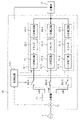
- FIG. 2 is a circuit diagram showing an exemplary configuration of the power conversion circuits 12-1 to 12-3 of FIG.
- the primary side circuit 21 includes diodes D1 to D4, capacitors C1 to C2, a power factor improving circuit 31, and switching elements Q1 to Q4.
- the diodes D1 to D4 rectify the AC power of the LN1 phase, the LN2 phase, or the LN3 phase input via any of the switches SW-1 to SW-3.
- the capacitor C1 smoothes the power rectified by the diodes D1 to D4.
- the power factor improving circuit 31 improves the power factor by suppressing the harmonics of the rectified and smoothed DC power.
- the switching elements Q1 to Q4 form a full-bridge type inverter circuit, and convert the DC power output from the power factor improving circuit 31 into AC power.
- the switching elements Q1 to Q4 are, for example, N-channel MOSFETs.
- the switching elements Q1 to Q4 are turned on / off according to a control signal applied to the gate from the control circuit 13.
- the capacitor C2 is connected between the switching elements Q1 to Q4 and the primary winding L1 of the transformer 22.
- the transformer 22 includes a primary winding L1 and a secondary winding L2.
- the primary winding L1 and the secondary winding L2 each have an exciting inductance.
- the transformer 22 further has a leakage inductance L3. The configuration of the transformer 22 will be described in more detail with reference to FIG.
- the secondary circuit 23 includes diodes D5 to D8 and a capacitor C3.
- the diodes D5 to D8 rectify the AC power generated in the secondary winding L2 of the transformer 22.
- the capacitor C3 smoothes the power rectified by the diodes D5 to D8.
- the rectified and smoothed DC power is supplied to the rechargeable battery 3.
- the exciting inductance of the primary winding L1 of the transformer 22, the leakage inductance L3, and the capacitor C2 form an LLC resonance circuit. Therefore, the switching elements Q1 to Q4 of the primary circuit 21, the capacitors C2, the transformer 22, and the secondary circuit 23 form an LLC resonance type DC / DC converter circuit.
- the LLC resonant DC / DC converter circuit is widely used in high-efficiency power supply devices such as industrial switching power supply devices, in-vehicle charging devices, and power converters.
- the control circuit 13 uses a frequency modulation method that changes the switching frequency of the switching elements Q1 to Q4 while monitoring the load voltage required to charge the rechargeable battery 3, and the power conversion circuits 12-1 to 12-3.
- the power conversion circuits 12-1 to 12-3 are controlled so that the output voltage of the above is close to the load voltage.
- the power conversion circuits 12-1 to 12-3 can reduce the switching loss by operating the switching elements Q1 to Q4 with zero voltage switching. Further, the power conversion circuits 12-1 to 12-3 can reduce the surge current and the voltage and reduce the noise by generating a switching current close to a sine wave.
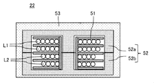
- FIG. 3 is a cross-sectional view showing an exemplary configuration of the transformers 22-1 to 22-3 of FIG.
- the transformer 22 includes a primary winding L1 and a secondary winding L2 as described above, and further includes a bobbin 51, a core 52, and a potting 53.
- the primary winding L1 and the secondary winding L2 are wound around the bobbin 51.
- the core 52 is composed of core portions 52a and 52b, and the core portions 52a and 52b sandwich a bobbin 51 around which the primary winding L1 and the secondary winding L2 are wound.
- the core 52 is made of, for example, ferrite.
- the core 52 is embedded in a potting 53 made of silicone rubber or the like.
- Copper loss occurs in the primary winding L1 and the secondary winding L2, iron loss occurs in the core 52, and the temperatures of the primary winding L1, the secondary winding L2, and the core 52 rise due to these losses. do.
- the heat of the primary winding L1, the secondary winding L2, and the core 52 is released to the outside through the potting 53. Further, by conducting heat to each other between the core portions 52a and 52b, the temperature difference between the core portions 52a and 52b can be reduced.
- the thermal conductivity of the material used for the potting 53 is about 1 to 2 W / (m ⁇ K), whereas the thermal conductivity of the ferrite used for the core 52 is 5 W / (m ⁇ K). ), And has high heat dissipation.
- the thickness of the potting 53 around the core 52 may be constant or may vary from place to place.
- the potting 53 at the bottom of the transformer 22 is more than any other portion. Is also getting thinner.
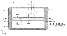
- FIG. 4 is a vertical cross-sectional view of a housing 41 for explaining the cooling device of the power conversion device 2 of FIG.
- FIG. 5 is a cross-sectional view of the housing 41 for explaining the cooling device of the power conversion device 2 of FIG.
- FIG. 5 shows a cross section taken along the line AA'of FIG.
- the power conversion device 2 further includes a housing 41, a radiator 45, and a pump 46.
- the housing 41 protects its internal components from water, dust, noise, and the like.
- the housing 41 is configured by fitting a plurality of parts formed by die-casting aluminum or the like to each other.
- the housing 41 includes chambers 42 to 44. Chambers 42, 43 accommodate each component of the power converter 2 shown in FIG.
- a cooling liquid 44a for example, cooling water or an antifreeze liquid called LLC (Long Life Coolant) circulates inside the chamber 44.
- the coolant 44a is in thermal contact with each component of the power converter 2 via the walls 44b, 44c of the chamber 44.
- the chamber 44 is connected to the radiator 45 and the pump 46 outside the housing 41 via the inlet 44d and the outlet 44e.
- the coolant 44a circulates in the chamber 44, the radiator 45, and the pump 46 by the pump 46.
- the heat generated by the heat generating components of the power conversion device 2 (primary side circuit 21, transformer 22, secondary side circuit 23, etc.) is transferred to the coolant 44a via the wall portions 44b, 44c, and is transferred to the coolant 44a.
- the heat is released from the radiator 45.
- the chamber 44 may include one or more fins 44f to improve cooling performance.
- FIG. 5 schematically shows the footprints of the primary side circuit 21, the transformer 22, and the secondary side circuit 23 of the power conversion circuit 12.
- the power conversion circuits 12-1 to 12-3 have the same configuration as each other, and therefore the primary side circuits 21-1 to 21-3 have the same dimensions as each other, and the transformers 22-1 to 22-1 to The case where 22-3 has the same size as each other and the secondary side circuits 23-1 to 23-3 have the same size as each other is shown.
- the chamber 44 is a flow path F1 to F3 for flowing the coolant 44a, and includes at least the flow paths F1 to F3 in thermal contact with the transformers 22-1 to 22-3, respectively. ..
- the flow paths F1 to F3 may further be in thermal contact with the primary side circuits 21-1 to 21-3 and the secondary side circuits 23-1 to 23-3, respectively.
- the primary side circuits 21-1 to 21-3, the transformers 22-1 to 22-3, and the secondary side circuits 23-1 to 23-3 pass through the wall portion 44b (see FIG. 4) of the chamber 44. It is in thermal contact with the flow paths F1 to F3.
- the flow paths F1 to F3 may be connected to each other at least partially.
- the housing 41, the radiator 45, and the pump 46 constitute a cooling device for the power conversion device 2, and cool the heat-generating components of the power conversion device 2.
- the magnitude of the load voltage required to charge the rechargeable battery 3 depends on the charging state of the rechargeable battery 3, that is, the charged voltage (hereinafter referred to as "voltage of the rechargeable battery 3"). It changes from the lower limit voltage to the fully charged voltage.
- the load current and the magnitude of the load power required for charging the rechargeable battery 3 also change depending on the charging state of the rechargeable battery 3.
- the power conversion device 2 changes the number of operating power conversion circuits 12-1 to 12-3 according to the load current or the magnitude of the load power required for charging the rechargeable battery 3.
- the power conversion device 2 operates all the power conversion circuits 12-1 to 12-3 in a heavy load state where a large current or a large power is required to charge the rechargeable battery 3, and the rechargeable battery 3 is charged. In a light load state where a small current or a small power is required for charging, only one of the power conversion circuits 12-1 to 12-3 is operated.
- the operation of the power conversion device 2 when operating all the power conversion circuits 12-1 to 12-3 is referred to as "heavy load operation", and among the power conversion circuits 12-1 to 12-3.
- the operation of the power conversion device 2 when only one is operated is called "light load operation".
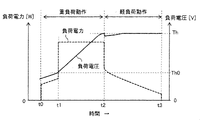
- FIG. 6 is a graph showing exemplary changes in load power and load voltage when the rechargeable battery 3 in FIG. 1 is charged.
- the power conversion device 2 starts charging the rechargeable battery 3
- the power conversion device 2 first operates all of the power conversion circuits 12-1 to 12-3 (heavy load operation).
- the power conversion device 2 operates all of the power conversion circuits 12-1 to 12-3 in order to prevent deterioration of the rechargeable battery 3.
- the rechargeable battery 3 is charged with a small amount of power.
- the power conversion device 2 charges the rechargeable battery 3 with a constant current, and the load power gradually increases as the load voltage rises.
- the power conversion device 2 Increases the output power of the power conversion circuits 12-1 to 12-3 and charges the rechargeable battery 3 with a constant high power.
- Th the voltage of the rechargeable battery 3 further increases and approaches the fully charged voltage Th
- an excessive voltage is applied to the rechargeable battery 3 by superimposing the voltage drop due to the internal resistance of the rechargeable battery 3 and the current on the load voltage. , The rechargeable battery 3 may be damaged and its life may be shortened.
- the power conversion device 2 operates only one of the power conversion circuits 12-1 to 12-3, and of the other power conversion circuits. Stop the operation (light load operation). Since the number of operating power conversion circuits 12-1 to 12-3 is reduced and the output current is reduced, the voltage drop of the rechargeable battery 3 is reduced, and as a result, the load voltage is temporarily lowered. After that, the operating power conversion circuit gradually reduces the current flowing through the rechargeable battery 3. By reducing the current flowing through the rechargeable battery 3, the voltage drop of the rechargeable battery 3 is further reduced, and the voltage of the rechargeable battery 3 approaches the fully charged voltage Th.
- the power conversion device 2 changes the number of operating power conversion circuits 12-1 to 12-3 according to the magnitude of the load voltage instead of the magnitude of the load current or the load power. Let me.
- FIG. 7 is a graph showing the temperature characteristics of the iron loss of the cores 52 of the transformers 22-1 to 22-3 of FIG.
- copper loss occurs due to the current flowing through the primary winding L1 and the secondary winding L2
- iron loss occurs due to the magnetic flux flowing through the core 52. Since a magnetic flux is generated by the exciting current flowing through the primary winding L1, the magnetic flux increases as the exciting current increases, and the iron loss increases. Further, the higher the output voltage, the higher the exciting current, and the smaller the output current, the higher the exciting current. Therefore, as the voltage of the rechargeable battery 3 approaches full charge and the output current of the power conversion circuit 12 is reduced, iron loss occurs. The amount of heat generated by the core 52 increases.
- Materials such as ferrite, which are generally used for the core 52 of the transformer 22, have the temperature characteristics of iron loss as shown in FIG. Iron loss is minimized at 80-90 ° C. When the temperature of the core 52 exceeds 80 to 90 ° C. during the operation of the power conversion circuit 12, the iron loss increases and the temperature of the core 52 further rises. As the temperature of the core 52 rises, the iron loss also increases. By repeating this cycle, thermal runaway may occur and the core 52 of the transformer 22 may be damaged. In order to reduce the thermal runaway of the transformer 22, it is important to reduce or manage the heat generated by the transformer 22.
- the primary side current of the transformer 22 includes a current component (that is, an exciting current) that contributes to the generation of magnetic flux and a current component that contributes to the generation of secondary side current.
- a current component that is, an exciting current
- the latter current component is dominant, and the power conversion circuit 12 operates with high efficiency.
- the output power and the output current decrease, the resonance current decreases, the exciting current that does not contribute to the generation of the secondary side current becomes dominant, and the efficiency of the power conversion circuit 12 decreases. Therefore, in the light load operation, by operating only one power conversion circuit without operating all of the power conversion circuits 12-1 to 12-3, the amount of decrease in the output current of the operating power conversion circuit is reduced. Can be reduced and the decrease in efficiency can be mitigated.
- the power conversion device 2 has a transformer 22 having the highest cooling performance when operating only one of a plurality of power conversion circuits 12 in a light load operation.
- the provided power conversion circuit 12 is operated.
- the bottom surface of the transformer 22 thermally contacts the flow paths F1 to F3 via the wall portion 44b of the chamber 44.
- the entire bottom surface thereof faces the flow path F2
- the transformers 22-1 and 22-3 a part of the bottom surface thereof flows. It faces the roads F1 and F3. Therefore, the area where the transformer 22-2 is in thermal contact with the flow path F2 is larger than the area where the transformers 22-1 and 22-3 are in thermal contact with the flow paths F1 and F3, respectively.
- the cooling performance of the transformer 22-2 becomes higher than the cooling performance of the transformers 22-1, 22-3.
- the control circuit 13 has a flow path among the plurality of power conversion circuits 12 when the power conversion device 2 operates with a light load, that is, when the load voltage of the rechargeable battery 3 becomes equal to or higher than a predetermined threshold value Th.
- the power conversion circuit 12 including the transformer 22 having the largest area of the region in thermal contact with F1 to F3 is operated, and the operation of the other power conversion circuits 12 is stopped. Therefore, in the example of FIG. 5, when the power conversion device 2 operates with a light load, the control circuit 13 operates only the power conversion circuit 12-2 and stops the operation of the power conversion circuits 12-1 and 12-3. ..
- the power conversion circuit 12 including the transformer 22 having the highest cooling performance can be operated. It operates and can make the core 52 less likely to be damaged due to overheating of the transformer 22 than before.
- FIG. 8 is a diagram showing heat conduction between transformers 22-1 to 22-3 when the transformers 22-1 to 22-3 of FIG. 1 are in thermal contact with each other.
- the transformer 22 of the power conversion circuit 12 that has stopped operating approaches the temperature of the coolant 44a in a relatively short time. Therefore, by arranging the transformers 22 of each power conversion circuit 12 so as to be in thermal contact with each other, heat is dissipated from the transformer 22 of the operating power conversion circuit 12 to the transformer 22 of the stopped power conversion circuit 12. Can be done. In particular, by contacting the transformer 22 of the power conversion circuit 12 in operation with the transformers 22 of the plurality of stopped power conversion circuits 12, the transformer 22 of one stopped power conversion circuit 12 is brought into contact with the transformer 22. Cooling performance is improved.
- the control circuit 13 operates one power conversion circuit 12 including a transformer 22 that is in thermal contact with at least two other transformers 22 among the plurality of power conversion circuits 12 when the power conversion device 2 operates with a light load.
- the operation of the other power conversion circuit 12 is stopped. Therefore, in the example of FIG. 8, the control circuit 13 operates only the power conversion circuit 12-2 including the transformer 22-2 when the power conversion device 2 operates with a light load, and the transformers 22-1 and 22-3 are operated.
- the operation of the power conversion circuits 12-1 and 12-3 provided is stopped. In this way, by operating one power conversion circuit 12 including a transformer 22 that is in thermal contact with at least two other transformers 22, the power conversion circuit 12 including the transformer 22 having the highest cooling performance operates. ,
- the damage of the core 52 due to the overheating of the transformer 22 can be made less likely to occur than before.
- each power conversion circuit 12 By arranging the transformers 22 of each power conversion circuit 12 so as to be in thermal contact with each other, even if there is no difference in the area of the region where the transformers 22 are in thermal contact with the flow paths F1 to F3. , The power conversion circuit 12 provided with the transformer 22 having the highest cooling performance can be operated. Further, by arranging each transformer 22 so that the transformer 22 having the largest area of the region in thermal contact with the flow paths F1 to F3 is in thermal contact with at least two other transformers 22, the transformer 22 is cooled. Performance can be further improved.
- FIG. 9 is a block diagram showing a configuration of a charging system including a power conversion device 2A according to a modification of the first embodiment.
- the power conversion device 2A includes a control circuit 13A instead of the control circuit 13 of FIG. 1, and further includes valves 47-1 to 47-3.
- the valves 47-1 to 47-3 pass or block the coolant 44a flowing through the flow paths F1 to F3, as will be described later with reference to FIGS. 10 and 11.
- the valves 47-1 to 47-3 are, for example, solenoid valves.
- the control circuit 13A controls the switches SW-1 to SW-3 and the power conversion circuits 12-1 to 12-3 in the same manner as the control circuit 13 of FIG. 1, and further opens and closes the valves 47-1 to 47-3. Control.
- valve 47 In this specification, valves 47-1 to 47-3 are collectively referred to as "valve 47".
- FIG. 10 is a vertical sectional view of a housing 41 for explaining the cooling device of the power conversion device 2A of FIG.
- FIG. 11 is a cross-sectional view of the housing 41 for explaining the cooling device of the power conversion device 2A of FIG.
- FIG. 11 shows a cross section taken along the line BB'of FIG.
- the chamber 44 includes a partition plate 44g that separates the flow paths F1 to F3 from each other.
- the valves 47-1 to 47-3 are provided in the flow paths F1 to F3, respectively, and pass or block the coolant 44a flowing in the flow paths F1 to F3.
- the control circuit 13A operates the power conversion circuit 12 of one of the plurality of power conversion circuits 12 and stops the operation of the other power conversion circuits 12 as described above. do. Further, the control circuit 13A opens the valves provided in the flow paths F1 to F3 that are in thermal contact with the transformer 22 of the operating power conversion circuit 12 when the power conversion device 2A operates with a light load, and is stopped.
- FIG. 11 shows a case where only the valve 47-2 is opened and the valves 47-1 and 47-3 are closed. In this way, by increasing the flow velocity of the flow paths F1 to F3 that are in thermal contact with the transformer 22 of the operating power conversion circuit 12, the cooling performance of the transformer 22 of the operating power conversion circuit 12 is improved. Damage to the core 52 due to overheating of the transformer 22 can be made less likely to occur than in the past.
- the present inventors have confirmed that when the iron loss of the core 52 is maximized, the temperature of the core 52 is lowered by 20 ° C. by increasing the flow rate from 4 liters / minute to 6 liters / minute. ..
- valve 47 is provided upstream of the transformer 22, but the valve 47 may be provided at any location along the flow paths F1 to F3, for example, downstream of the transformer 22. ..
- the valve 47 does not need to completely block the flow paths F1 to F3, and the flow velocity of the open flow path can be increased by partially making the flow path difficult.
- the valve 47 By using the valve 47, even when there is no difference in the area of the region where the transformer 22 is in thermal contact with the flow paths F1 to F3, the transformer 22 of the operating power conversion circuit 12 can be cooled satisfactorily. Can be done. Further, the control circuit 13A operates when the power conversion circuit 12 including the transformer 22 having the largest area in the region thermally contacted with the flow paths F1 to F3 is operated and the operation of the other power conversion circuits 12 is stopped. The valves 47 provided in the flow paths F1 to F3 that are in thermal contact with the transformer 22 of the power conversion circuit 12 inside are opened, and the flow paths F1 to F3 that are in thermal contact with the transformer 22 of the stopped power conversion circuit 12 are opened. The valve 47 provided in may be closed. Thereby, the cooling performance of the transformer 22 can be further improved.
- the transformer 22 of the operating power conversion circuit 12 can be satisfactorily cooled even when the transformers 22 of each power conversion circuit 12 are not in thermal contact with each other.
- the control circuit 13A is in operation when operating one power conversion circuit 12 including a transformer 22 that is in thermal contact with at least two other transformers 22 and stopping the operation of the other power conversion circuit 12.
- the valves 47 provided in the flow paths F1 to F3 that are in thermal contact with the transformer 22 of the power conversion circuit 12 are opened, and are provided in the flow paths F1 to F3 that are in thermal contact with the transformer 22 of the stopped power conversion circuit 12.
- the closed valve 47 may be closed. Thereby, the cooling performance of the transformer 22 can be further improved.
- the transformer 22 having the highest cooling performance when operating only one of the plurality of power conversion circuits 12 is provided.
- the power conversion circuit 12 can be operated.
- the core 52 can be less likely to be damaged due to overheating of the transformer 22, and the reliability of the power conversion device 2.2A can be improved.
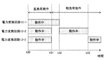
- FIG. 12 is a graph schematically showing the temporal change in the temperature of the core 52 of the transformers 22-1 to 22-3 when the power conversion device 2 of FIG. 1 is switched from the heavy load operation to the light load operation.
- FIG. 12 shows a case where the transformers 22-1 to 22-3 of the power conversion device 2 of FIG. 1 do not have sufficient cooling performance.
- the temperatures of the cores 52 of the transformers 22-1 to 22-3 are equal to each other.
- the power conversion device 2 operates with a light load, in the example of FIG.
- the transformer 22- when only the power conversion circuit 12-1 operates and the operations of the power conversion circuits 12-2 and 12-3 stop, the transformer 22-
- the temperature of the core 52 of 1 rises substantially linearly at a rate of about 0.01 ° C./sec, and the temperature of the core 52 of the transformers 22-2 and 22-3 linearly rises at a rate of about 0.1 ° C./sec. Decreases to. If the operation shown in FIG. 12 is continued, the core 52 of the transformer 22-1 may overheat and be damaged. Therefore, in the second embodiment, the control circuit 13 has a plurality of power conversion circuits when the power conversion device 2 operates with a light load, that is, when the load voltage of the rechargeable battery 3 becomes equal to or higher than the threshold value Th. A plurality of power conversion circuits 12 are selectively and sequentially operated so that one of the power conversion circuits 12 operates and the operation of the other power conversion circuit 12 stops.
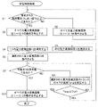
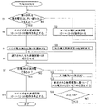
- FIG. 13 is a flowchart showing a charge control process executed by the control circuit 13 of the power conversion device 2 according to the second embodiment.
- step S1 the control circuit 13 determines whether or not the magnitude of the load voltage required for charging the rechargeable battery 3 is equal to or greater than a predetermined threshold value Th, and if YES, step S3. If NO, proceed to step S2.
- the threshold value Th is set to the fully charged voltage of the rechargeable battery 3, for example, as described with reference to FIG.
- step S2 the control circuit 13 turns on and operates all the power conversion circuits 12-1 to 12-3 (heavy load operation), and then periodically returns to step S1.
- step S3 the control circuit 13 stops the operation of all the power conversion circuits 12-1 to 12-3.
- step S4 the control circuit 13 selects one of the power conversion circuits 12-1 to 12-3.
- step S5 the control circuit 13 turns on and operates the selected power conversion circuit 12 (light load operation), and starts supplying power to the rechargeable battery 3.
- step S6 the control circuit 13 starts timing the operation time of the selected power conversion circuit 12.
- step S7 the control circuit 13 determines whether or not the rechargeable battery 3 has reached full charge, and if YES, the process proceeds to step S10, and if NO, the process proceeds to step S8.
- step S8 the control circuit 13 determines whether or not the operating time for the selected power conversion circuit 12, that is, the predetermined time period for the selected power conversion circuit 12 has expired, and YES. When, the process proceeds to step S9, and when NO, the process returns to step S7.
- step S9 the control circuit 13 selects the next power conversion circuit 12 from the power conversion circuits 12-1 to 12-3 in a predetermined order, and returns to step S5.
- the power conversion circuit 12-2 operates next to the power conversion circuit 12-1
- the power conversion circuit 12-3 operates next to the power conversion circuit 12-2, and the power is generated.
- the power conversion circuit 12-1 operates next to the conversion circuit 12-3, and thereafter, the power conversion circuits 12-1 to 12-3 operate selectively and sequentially.
- step S10 the control circuit 13 stops the operation of all the power conversion circuits 12-1 to 12-3.
- FIG. 14 is a timing chart showing the operation of the power conversion circuits 12-1 to 12-3 when the charge control process of FIG. 13 is executed.
- the power conversion device 2 operates with a heavy load
- steps S3 to S9 of FIG. 13 the power conversion device 2 operates with a light load.
- the control circuit 13 switches the operating power conversion circuit 12 among the power conversion circuits 12-1 to 12-3 every time a predetermined time period elapses.
- the power conversion circuits 12-1 to 12-3 operate, for example, for the same period of time.
- each of the power conversion circuits 12-1 to 12-3 operates during a 1/3 time period, and operates during the remaining 2/3 time period. Stop.
- the temperature decrease rate of the core 52 of the transformer 22 in the stopped power conversion circuit 12 is the temperature increase rate of the core 52 of the transformer 22 in the operating power conversion circuit 12. It is 10 times. Therefore, as shown in FIG. 14, when the power conversion device 2 operates with a light load, the temperature of the core 52 does not rise effectively by switching the operating power conversion circuit 12.
- the time period of step S8 in FIG. 13 is determined based on the temperature rise rate of the core 52, the temperature decrease rate of the core 52, the upper limit of the temperature at which thermal runaway does not occur, and the like.
- the time period of step S8 in FIG. 13 may be set to, for example, 1 minute or 2 minutes in order to disperse the core 52 that rises in temperature.
- the time period of step S8 in FIG. 13 may be the same or different for the plurality of power conversion circuits 12.
- the control circuit 13 is a plurality of power conversion circuits so that when the power conversion device 2 operates under a light load, the total operating time lengths of the power conversion circuits 12 over a predetermined long time period are equal to each other. 12 may be operated selectively and sequentially. Further, the control circuit 13 selects a plurality of power conversion circuits 12 so as to allocate a longer operating time to the power conversion circuit 12 including the transformer 22 having higher cooling performance when the power conversion device 2 operates with a light load. It may be operated in a targeted and sequential manner. For example, as described above, the transformer 22 that is in thermal contact with the flow paths F1 to F3 in a larger area has higher cooling performance, and the transformer 22 that is in thermal contact with more transformers 22 has higher cooling performance. , Has higher cooling performance.
- FIG. 15 is a block diagram showing a configuration of a charging system including a power conversion device 2B according to a first modification of the second embodiment.
- the power conversion device 2B includes a control circuit 13B instead of the control circuit 13 of FIG. 1, and further includes temperature sensors 14-1 to 14-3.
- the temperature sensors 14-1 to 14-3 measure the temperature of the core 52 of the transformers 22-1 to 22-3, respectively.
- the control circuit 13B executes the charge control process described with reference to FIG. 16 based on the temperature of the core 52 measured by the temperature sensors 14-1 to 14-3.
- FIG. 16 is a flowchart showing a charge control process executed by the control circuit 13B of the power conversion device 2B of FIG.
- the charge control process of FIG. 16 includes steps S21 to S22 instead of steps S6 and S8 of FIG.
- the control circuit 13B proceeds to step S7 after step S5, and when step S7 is NO, proceeds to step S21.
- step S21 the control circuit 13B measures the temperature Temp of the core 52 of the transformer 22 in the selected power conversion circuit 12.
- step S22 the control circuit 13B determines whether or not the temperature Temp is equal to or higher than the predetermined threshold value ThA. If YES, the process proceeds to step S9, and if NO, the process returns to step S7.
- the threshold value ThA may be set to, for example, a temperature at which the iron loss of the core 52 shown in FIG. 7 is minimized, that is, a temperature at which the iron loss of the core 52 begins to increase, which is 80 ° C. to 90 ° C.
- the control circuit 13B receives each time the temperature of the transformer 22 of the operating power conversion circuit 12 becomes equal to or higher than the threshold value ThA when the power conversion device 2B operates with a light load. , The operating power conversion circuit 12 is switched.
- FIG. 17 is a graph schematically showing the temporal change in the temperature of the core 52 of the transformers 22-1 to 22-3 when the charge control process of FIG. 16 is executed.
- FIG. 18 is a timing chart showing the operation of the power conversion circuits 12-1 to 12-3 when the charge control process of FIG. 16 is executed.
- step S2 of FIG. 16 the power conversion device 2B operates with a heavy load
- steps S3 to S5, S7, S21, S22, and S9 of FIG. 16 the power conversion device 2B operates with a light load.
- the power conversion circuit 12-1 when the light load operation is started, the power conversion circuit 12-1 operates first.
- the temperature of the core 52 of the transformer 22-1 rises due to iron loss of the core 52 and the like.
- the control circuit 13B monitors the temperature of the core 52 of the transformer 22-1, and when the temperature of the core 52 exceeds the threshold value ThA, the operation of the power conversion circuit 12-1 is stopped, and the power conversion circuit 12- The operation of 2 is started. As a result, the temperature of the core 52 of the transformer 22-1 of the stopped power conversion circuit 12-1 starts to decrease and quickly approaches the temperature of the coolant 44a.
- the core 52 of the transformer 22-2 of the power conversion circuit 12-2 is cooled before the power conversion circuit 12-2 starts operation, but gradually rises as the power conversion circuit 12-2 starts operation. do.
- the control circuit 13B monitors the temperature of the core 52 of the transformer 22-2, and when the temperature of the core 52 exceeds the threshold value ThA, the operation of the power conversion circuit 12-2 is stopped, and the power conversion circuit 12- The operation of 3 is started.
- the power converter 2B operates under a light load, the iron loss of the core 52 increases remarkably, but the unbalanced temperature distribution of the core 52 does not occur, which makes it difficult for the core 52 to be damaged and provides high reliability.
- the power conversion device 2B having the power conversion device 2B is obtained.
- the control circuit 13B operates in the range of around 80 to 90 ° C., for example, 70 to 100 ° C., where the iron loss is minimized. As such, the operating power conversion circuit 12 may be switched. As a result, the power conversion device 2B can operate with high efficiency even during a light load operation in which efficiency generally decreases.
- FIG. 19 is a block diagram showing a configuration of a charging system including a power conversion device 2C according to a second modification of the second embodiment.
- the power conversion device 2C includes a control circuit 13C instead of the control circuit 13 of FIG. 1, and further includes a current sensor 15.
- the current sensor 15 measures the input current of each power conversion circuit 12.
- the control circuit 13C executes the charge control process described with reference to FIG. 20 based on the input current measured by the current sensor 15.
- FIG. 20 is a flowchart showing a charge control process executed by the control circuit 13C of the power conversion device 2C of FIG.
- the charge control process of FIG. 20 includes steps S31 to S33 instead of steps S21 to S22 of FIG.
- the control circuit 13C proceeds to step S31 when step S7 is NO.
- step S31 the control circuit 13C measures the input current Iin of the selected power conversion circuit 12.
- step S32 the control circuit 13C sets the threshold value ThB of the input current based on the magnitude of the load current required for charging the rechargeable battery 3.
- step S33 the control circuit 13C determines whether or not the input current Iin is equal to or higher than the threshold value ThB. If YES, the process proceeds to step S9, and if NO, the process returns to step S7.
- the control circuit 13C determines the input current of the power conversion circuit 12 during operation based on the load current of the rechargeable battery 3 when the power conversion device 2C operates with a light load.
- the operating power conversion circuit 12 is switched each time the threshold value ThB or higher is reached.
- the output current of the power conversion circuit 12 is controlled based on the magnitude of the load current required to charge the rechargeable battery 3.
- the control circuit 13C measures the input current Iin of the primary circuit 21 of the transformer 22, and switches the operating power conversion circuit 12 when the input current Iin becomes equal to or higher than a predetermined threshold value ThB.
- ThB the threshold value
- the control circuit 13C can be used when the load current changes. Recalculate the threshold ThB. In this way, by selectively and sequentially operating the plurality of power conversion circuits 12 based on the input current Iin, it is possible to make it less likely that the core 52 is damaged due to overheating of the transformer 22.
- each power conversion circuit 12-1 to 12-3 when the power conversion device 2C operates with a light load, only one of the power conversion circuits 12-1 to 12-3 operates. Therefore, as shown in FIG. 19, 1 provided upstream of the distributor 11.
- the input current of each power conversion circuit 12-1 to 12-3 can be measured by using one current sensor 15. Instead, a current sensor for measuring the input current of each power conversion circuit 12-1 to 12-3 may be provided for each power conversion circuit 12-1 to 12-3.
- FIG. 21 is a block diagram showing a configuration of a charging system including a power conversion device 2D according to a third modification of the second embodiment.
- the power conversion device 2D includes a control circuit 13D instead of the control circuit 13 of FIG. 1, and further includes a power sensor 16.
- the power sensor 16 measures the input power of each power conversion circuit 12.
- the power sensor 16 may be a single sensor or a combination of a current sensor and a voltage sensor.
- the control circuit 13D executes the charge control process described with reference to FIG. 22 based on the input power measured by the power sensor 16.
- FIG. 22 is a flowchart showing a charge control process executed by the control circuit 13D of the power conversion device 2D of FIG. 21.
- the charge control process of FIG. 22 includes steps S41 to S43 instead of steps S21 to S22 of FIG.
- the control circuit 13D proceeds to step S41 when step S7 is NO.
- step S41 the control circuit 13D measures the input power Pin of the selected power conversion circuit 12.
- the control circuit 13D receives from the rechargeable battery 3 a control signal indicating the magnitude of the load current and the load voltage required for charging the rechargeable battery 3, and calculates the load power Pout based on the load current and the load voltage. You may. Further, the control circuit 13D may receive a control signal indicating the magnitude of the load power Pout from the rechargeable battery 3.
- step S43 the control circuit 13D determines whether or not the efficiency Eff is equal to or less than the predetermined threshold value ThC. If YES, the process proceeds to step S9, and if NO, the process returns to step S7.
- the control circuit 13D is operating based on the input power of the operating power conversion circuit 12 and the load power of the rechargeable battery 3 when the power conversion device 2D operates with a light load.
- the efficiency of the power conversion circuit 12 is calculated, and the operating power conversion circuit 12 is switched every time the efficiency becomes equal to or less than the threshold value ThC.
- the power conversion device 2D operates with a light load, only one of the power conversion circuits 12-1 to 12-3 operates. Therefore, as shown in FIG. 21, 1 provided upstream of the distributor 11. Using one power sensor 16, the input power of each power conversion circuit 12-1 to 12-3 can be measured. Instead, a power sensor for measuring the input power of each power conversion circuit 12-1 to 12-3 may be provided for each power conversion circuit 12-1 to 12-3.
- the plurality of power conversion circuits 12 are selectively and sequentially operated even if the cooling device as shown in FIGS. 4 and 5 is not provided. By doing so, the temperature of the core 52 of the transformer 22 is less likely to rise than before.
- the valve 47 described with reference to FIGS. 9 to 11 may be applied to the power conversion devices 2, 2B to 2D according to the second embodiment.
- the control circuits 13, 13B to 13D open the valves provided in the flow paths F1 to F3 that are in thermal contact with the transformer 22 of the power conversion circuit 12 in operation, and the transformer of the power conversion circuit 12 that is stopped is stopped. Close the valves provided in the flow paths F1 to F3 that are in thermal contact with 22. Thereby, the cooling performance of the transformer 22 can be further improved.
- the power conversion device 2 transitions from the heavy load operation to the light load operation.
- the power conversion device 2 may transition from the heavy load operation to the light load operation when the load voltage becomes equal to or higher than a predetermined threshold value lower than the fully charged voltage Th.
- the power conversion device 2 may transition from a heavy load operation to a light load operation based on the load current or load power required to charge the rechargeable battery 3.
- the power conversion device includes the primary side circuit 21, the secondary side circuit 23, and / or other heat generation. It may be configured to prevent overheating of the component.
- the power conversion device 2 receives, for example, a three-phase AC power supply from a three-phase AC power supply 1
- the power conversion device according to the embodiment of the present disclosure is a single or a plurality of single-phase power conversion devices. It may be configured to receive power from a phase AC power source or may be configured to receive power from one two-phase AC power source.
- the distributor 11 may supply the same AC power to the three power conversion circuits 12. Further, when the power conversion device receives power from two single-phase AC power supplies, the distributor 11 supplies the AC power of one AC power supply to one power conversion circuit 12, and supplies the AC power of the other AC power supply.
- the control circuit 13 stops the operation of the remaining one power conversion circuit 12.
- the distributor 11 may supply the AC power of each AC power supply to each power conversion circuit 12 on a one-to-one basis.
- the distributor 11 supplies AC power of one phase to one power conversion circuit 12, and converts AC power of another phase into another power. It may be supplied to the circuit 12. In this case, the control circuit 13 stops the operation of the remaining one power conversion circuit 12.
- the power conversion device may be configured to receive power from one or more DC power sources.
- the distributor 11 supplies power to the three power conversion circuits 12 as in the case of receiving power from one or a plurality of single-phase AC power supplies, and the primary side circuit 21 of each power conversion circuit 12.
- the diodes D1 to D4 and the power factor improving circuit 31 of the above are omitted.
- the power conversion device may include two or four or more power conversion circuits.
- the power conversion device is not limited to the power conversion circuit 12 including the LLC resonance type DC / DC converter circuit, and may include any power conversion circuit including a transformer.
- the power conversion device is not limited to the rechargeable battery 3, and may be configured to supply DC power to any load device in which the magnitude of the load voltage changes.
- the power conversion device is applicable to, for example, an in-vehicle charging system for an electric vehicle or a plug-in hybrid vehicle.
Landscapes
- Engineering & Computer Science (AREA)
- Power Engineering (AREA)
- Dc-Dc Converters (AREA)
Abstract
Priority Applications (4)
| Application Number | Priority Date | Filing Date | Title |
|---|---|---|---|
| US18/271,189 US20240055995A1 (en) | 2021-01-07 | 2021-12-27 | Electric power conversion apparatus capable of controlling power conversion circuits to operate selectively and sequentially |
| CN202180089362.0A CN116711182A (zh) | 2021-01-07 | 2021-12-27 | 电力变换装置 |
| EP21917746.6A EP4277080A1 (fr) | 2021-01-07 | 2021-12-27 | Dispositif de conversion d'énergie électrique |
| JP2022574027A JPWO2022149526A1 (fr) | 2021-01-07 | 2021-12-27 |
Applications Claiming Priority (2)
| Application Number | Priority Date | Filing Date | Title |
|---|---|---|---|
| JP2021-001557 | 2021-01-07 | ||
| JP2021001557 | 2021-01-07 |
Publications (1)
| Publication Number | Publication Date |
|---|---|
| WO2022149526A1 true WO2022149526A1 (fr) | 2022-07-14 |
Family
ID=82357946
Family Applications (1)
| Application Number | Title | Priority Date | Filing Date |
|---|---|---|---|
| PCT/JP2021/048555 WO2022149526A1 (fr) | 2021-01-07 | 2021-12-27 | Dispositif de conversion d'énergie électrique |
Country Status (5)
| Country | Link |
|---|---|
| US (1) | US20240055995A1 (fr) |
| EP (1) | EP4277080A1 (fr) |
| JP (1) | JPWO2022149526A1 (fr) |
| CN (1) | CN116711182A (fr) |
| WO (1) | WO2022149526A1 (fr) |
Citations (6)
| Publication number | Priority date | Publication date | Assignee | Title |
|---|---|---|---|---|
| JPH029472B2 (fr) | 1983-07-19 | 1990-03-02 | Nippon Electric Co | |
| JPH0343678B2 (fr) | 1983-10-18 | 1991-07-03 | Matsushita Electric Ind Co Ltd | |
| JPH10271823A (ja) * | 1997-03-21 | 1998-10-09 | Shindengen Electric Mfg Co Ltd | 3相力率改善型コンバータ |
| JP2008187865A (ja) * | 2007-01-31 | 2008-08-14 | Nagano Japan Radio Co | 充電装置 |
| JP2010233439A (ja) * | 2009-03-03 | 2010-10-14 | Toshiba Corp | 電源制御装置、及びそれを用いた電源装置 |
| JP2014236620A (ja) * | 2013-06-04 | 2014-12-15 | 三菱電機株式会社 | 電力変換装置 |
-
2021
- 2021-12-27 EP EP21917746.6A patent/EP4277080A1/fr active Pending
- 2021-12-27 WO PCT/JP2021/048555 patent/WO2022149526A1/fr active Application Filing
- 2021-12-27 JP JP2022574027A patent/JPWO2022149526A1/ja active Pending
- 2021-12-27 US US18/271,189 patent/US20240055995A1/en active Pending
- 2021-12-27 CN CN202180089362.0A patent/CN116711182A/zh active Pending
Patent Citations (6)
| Publication number | Priority date | Publication date | Assignee | Title |
|---|---|---|---|---|
| JPH029472B2 (fr) | 1983-07-19 | 1990-03-02 | Nippon Electric Co | |
| JPH0343678B2 (fr) | 1983-10-18 | 1991-07-03 | Matsushita Electric Ind Co Ltd | |
| JPH10271823A (ja) * | 1997-03-21 | 1998-10-09 | Shindengen Electric Mfg Co Ltd | 3相力率改善型コンバータ |
| JP2008187865A (ja) * | 2007-01-31 | 2008-08-14 | Nagano Japan Radio Co | 充電装置 |
| JP2010233439A (ja) * | 2009-03-03 | 2010-10-14 | Toshiba Corp | 電源制御装置、及びそれを用いた電源装置 |
| JP2014236620A (ja) * | 2013-06-04 | 2014-12-15 | 三菱電機株式会社 | 電力変換装置 |
Also Published As
| Publication number | Publication date |
|---|---|
| JPWO2022149526A1 (fr) | 2022-07-14 |
| EP4277080A1 (fr) | 2023-11-15 |
| US20240055995A1 (en) | 2024-02-15 |
| CN116711182A (zh) | 2023-09-05 |
Similar Documents
| Publication | Publication Date | Title |
|---|---|---|
| US10780795B2 (en) | Battery heating system and control method thereof | |
| Yang et al. | Double-phase high-efficiency, wide load range high-voltage/low-voltage LLC DC/DC converter for electric/hybrid vehicles | |
| JP5492599B2 (ja) | 回転電機システム | |
| JP5035978B2 (ja) | 車両用dcdcコンバータ装置 | |
| KR101241221B1 (ko) | 마일드 하이브리드 차량용 충전 장치 | |
| US11430596B2 (en) | Temperature regulating device for magnetic circuit component | |
| WO2012144249A1 (fr) | Dispositif de conversion de puissance et dispositif d'alimentation électrique à bord de véhicule doté de celui-ci | |
| US10141862B1 (en) | Power supply device | |
| JP6513211B2 (ja) | 車両用モータ制御装置および車両用モータ制御方法 | |
| JP2008108509A (ja) | 電池搭載装置、温度調整システム | |
| CN110504505B (zh) | 用于蓄电池的温度调节的装置和方法、蓄电池单元 | |
| WO2015087129A1 (fr) | Convertisseur de puissance | |
| CN111886789B (zh) | 功率转换装置 | |
| WO2022149526A1 (fr) | Dispositif de conversion d'énergie électrique | |
| WO2022149525A1 (fr) | Dispositif de conversion de puissance | |
| WO2013001595A1 (fr) | Unité de logement d'élément capacitif | |
| WO2020235500A1 (fr) | Dispositif de conversion de puissance et unité d'entraînement électrique | |
| JP5420080B2 (ja) | 電力変換装置 | |
| JP7320783B2 (ja) | 電力変換装置 | |
| JP5369753B2 (ja) | 電源システム | |
| JP6961047B1 (ja) | 電力変換装置 | |
| JP2019009959A (ja) | 電力変換装置 | |
| Reigosa et al. | A Framework for Reliability Analysis of a SiC Converter for Automotive On-Board Charger Applications | |
| Christian | Design Approaches to Enhance Power Density in Power Converters for Traction Applications | |
| JP2015065785A (ja) | 双方向dc/dcコンバータ装置 |
Legal Events
| Date | Code | Title | Description |
|---|---|---|---|
| 121 | Ep: the epo has been informed by wipo that ep was designated in this application |
Ref document number: 21917746 Country of ref document: EP Kind code of ref document: A1 |
|
| ENP | Entry into the national phase |
Ref document number: 2022574027 Country of ref document: JP Kind code of ref document: A |
|
| WWE | Wipo information: entry into national phase |
Ref document number: 202180089362.0 Country of ref document: CN |
|
| WWE | Wipo information: entry into national phase |
Ref document number: 18271189 Country of ref document: US |
|
| NENP | Non-entry into the national phase |
Ref country code: DE |
|
| ENP | Entry into the national phase |
Ref document number: 2021917746 Country of ref document: EP Effective date: 20230807 |