WO2022137653A1 - 電子制御装置 - Google Patents
電子制御装置 Download PDFInfo
- Publication number
- WO2022137653A1 WO2022137653A1 PCT/JP2021/031897 JP2021031897W WO2022137653A1 WO 2022137653 A1 WO2022137653 A1 WO 2022137653A1 JP 2021031897 W JP2021031897 W JP 2021031897W WO 2022137653 A1 WO2022137653 A1 WO 2022137653A1
- Authority
- WO
- WIPO (PCT)
- Prior art keywords
- control device
- electronic control
- protrusion
- hole
- circuit board
- Prior art date
- Legal status (The legal status is an assumption and is not a legal conclusion. Google has not performed a legal analysis and makes no representation as to the accuracy of the status listed.)
- Ceased
Links
Images




Classifications
-
- H—ELECTRICITY
- H10—SEMICONDUCTOR DEVICES; ELECTRIC SOLID-STATE DEVICES NOT OTHERWISE PROVIDED FOR
- H10W—GENERIC PACKAGES, INTERCONNECTIONS, CONNECTORS OR OTHER CONSTRUCTIONAL DETAILS OF DEVICES COVERED BY CLASS H10
- H10W74/00—Encapsulations, e.g. protective coatings
- H10W74/40—Encapsulations, e.g. protective coatings characterised by their materials
Definitions
- the present invention relates to an electronic control device.
- the in-vehicle electronic control device is equipped with a microcomputer that supports high-speed calculation and high-speed processing in order to realize advanced automatic driving functions, and the computing power of the microcomputers is increasing year by year as the required automatic driving functions become more sophisticated. And the calorific value is increasing proportionally.
- Patent Document 1 discloses "a heat dissipation structure in an electronic component accommodating case body". It is composed of a circuit board on which heat-generating electronic components are mounted and a case body that houses the circuit board, and the case body is formed by two case bodies so as to cover the front surface side and the back surface side of the circuit board. The body is integrally provided with a heat transfer protrusion that comes into contact with the heat-generating electronic component, heat can be dissipated to the case body via the heat transfer protrusion, and a circuit using the protrusion of the housing case is used. It is a heat dissipation structure that is also used as a alignment pin of a substrate, and provides a heat dissipation structure in an electronic component storage case body that allows easy assembly of components.
- the heat dissipation structure of Patent Document 1 has a structure in which the heat transfer protrusion extending from the case body touches the surface of the circuit board or the heat-generating electronic component. Therefore, the distance between the heat transfer protrusion and the heat source is not equal on the front surface side and the back surface side, and the heat transfer amount is biased to either one, so that the heat dissipation efficiency cannot be maximized.
- An object of the present invention is to provide an electronic control device capable of improving heat dissipation efficiency.
- the electronic control device of the present invention includes a circuit board on which a heat generating component is mounted and having a through hole, and a first housing having a first protrusion protruding toward the through hole. Thermal paste that conducts heat from the inner wall of the circuit board forming the through hole and the second housing having the second protrusion facing the first protrusion to the first protrusion and the second protrusion. And.
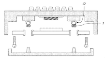
- FIG. It is sectional drawing (development view) of Embodiment 1.
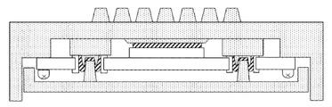
- FIG. It is sectional drawing (assembly drawing) of Embodiment 1.
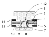
- FIG. It is sectional drawing (development view) of Embodiment 2.
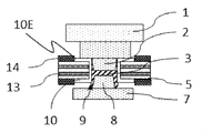
- FIG. It is a structural example 1 of a through hole portion. It is a structural example 2 of the through hole portion. It is a structural example 3 of the through hole portion.
- FIG. 1 is an example of a configuration diagram of a heat dissipation structure according to the present embodiment.
- the electronic control device 100 has a configuration in which a circuit board 5 is sandwiched between a base member 1 and a cover member 7, and the circuit board 5 is fixed to the base member 1 with fasteners such as screws 6.
- the base member projecting portion 2 extends from the base member 1, and the cover member projecting portion 8 extends from the cover member 7 so as to face each other.
- the circuit board 5 is provided with a through hole 9, and is arranged at a position where the base member projecting portion 2 and the cover member projecting portion 8 arranged to face each other are simultaneously inserted.
- Thermal paste 3 is applied to the tip of the base member protrusion 2 or the cover member protrusion 8, and the electronic control device 100 is assembled with a fastening member such as a screw (not shown) to the wall of the through hole 9 and the base.
- the member projecting portion 2 and the cover member projecting portion 8 are thermally connected via the thermal paste 3.
- the thermal paste 3 uses various types of materials such as grease and gel. Generally used is a grease-like heat conductive material, such as a thermosetting resin having adhesiveness and a semi-curing resin having low elasticity. Further, the conductive and non-conductive thermal paste 3 is selected and used in consideration of the mounting situation and the like.
- the thermal paste 3 is preferably a semi-cured resin using a silicon-based resin containing a ceramic filler, which has flexibility that can be deformed by heat deformation and vibration of the circuit board 5 and tolerance during manufacturing, for example. ..
- the thermal paste 3 and the circuit board 5 are arranged on substantially the same plane.
- the heat generating component 4 is electrically connected to the circuit board 5 with a joining material such as solder.
- the heat generated from the heat generating component 4 is transferred to the circuit board 5 via a bonding material such as solder, and the heat accumulated on the circuit board is thermally connected from the through hole 9 via the thermal paste 3 to the protruding portion of the base member. It is transmitted to 2 and the protruding portion 8 of the cover member, and heat is dissipated to the base member 1 and the cover member 7.
- the through hole 9 is covered with plating 10 and is electrically connected to the heat generating component 4 through a GND pattern or the like. The heat released from the heat generating component 4 is efficiently transferred to the plating 10 through the wiring pattern.
- the base member protruding portion 2 When the plated portion connected to the GND pattern, the base member protruding portion 2, the cover member protruding portion 8 or both are connected, the equipotential properties of the circuit board 5, the base member 1, and the cover member 7 are improved.
- the EMC resistance can be improved.
- a pedestal 11 for keeping the thermal paste 3 on substantially the same plane of the circuit board 5 is provided between the base member 1 and the base member protruding portion 2.
- the diameter of the pedestal 11 is larger than that of the through hole 9.
- the shape of the through hole 9 shown in FIGS. 9, 10 and 11 has variations such as a circle and an elongated hole, and the larger the diameter of the through hole 9, the more the base member 1 and the cover member 7 come into contact with each other via the thermal paste 3.
- heat can be dissipated from the circuit board 5 to the base member 1 and the cover member 7 more efficiently.
- the four corners of the through hole 9 are shaped with R so that plating can be applied.
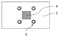
- the through hole 9 may be arranged near the heat generating component 4, the edge of the board, or the like, and if it is arranged near the heat generating component 4, heat can be dissipated before it spreads over the entire circuit board, so that heat can be efficiently dissipated.
- the through hole 9 is arranged at the end of the board, a space for mounting and wiring the component can be secured around the heat generating component 4, and the circuit board 5 is installed at the edge of the board when the circuit board 5 is fastened to the base member 1.
- the base member 1 and the cover member 7 are each made of a metal material having excellent thermal conductivity, such as aluminum (for example, ADC12). Further, it can be formed of a sheet metal such as iron or a non-metal material such as a resin material to reduce the cost and weight. Similarly, the cover member 7 can be formed of a sheet metal such as iron or a non-metal material such as a resin material.
- the electronic control device 100 includes at least a circuit board 5, a first housing (base member 1), a second housing (cover member 7), and thermal paste 3.
- the circuit board 5 is mounted with a heat generating component 4 and has a through hole 9.
- the first housing (base member 1) has a first protruding portion (pedestal 11) that protrudes toward the through hole 9.
- the second housing (cover member 7) has a second protruding portion (cover member protruding portion 8) facing the first protruding portion (pedestal 11).
- the thermal paste 3 conducts heat from the inner wall of the circuit board 5 forming the through hole 9 to the first protruding portion (pedestal 11) and the second protruding portion (cover member protruding portion 8).
- the heat of the heat generating component 4 is transferred to the inner wall of the circuit board 5 forming the through hole 9, the thermal paste 3, the first protruding portion (pedestal 11), the second protruding portion (cover member protruding portion 8), and the first casing. Heat is dissipated into the atmosphere via the body (base member 1) and the second housing (cover member 7).
- the base member 1 and the cover member 7 are referred to as a first housing and a second housing, respectively, but the opposite may be used.
- the pedestal 11 is provided on the base member 1, it may be provided on the cover member 7.
- the first protruding portion (pedestal 11) has a convex portion (base member protruding portion 2) facing the second protruding portion (cover member protruding portion 8).
- the thermal paste 3 is filled between the inner wall of the circuit board 5 forming the through hole 9 and the convex portion (base member projecting portion 2) and the second projecting portion (cover member projecting portion 8).
- the heat of the heat generating component 4 is transferred to the inner wall of the circuit board 5 forming the through hole 9, the thermal paste 3, the convex portion (base member projecting portion 2), the first projecting portion (pedestal 11), and the second projecting portion (the pedestal 11). Heat is dissipated into the atmosphere via the cover member projecting portion 8), the first housing (base member 1), and the second housing (cover member 7).
- the tip of the convex portion (base member protruding portion 2) is located inside the through hole 9.
- the first protrusion (pedestal 11) closes the through hole 9.
- the thermal paste 3 does not leak to the surface side of the circuit board 5 on which the heat generating component 4 is mounted.
- the base member 1 is on the lower side in the vertical direction at the time of assembly, and the circuit board 5 can be supported by the pedestal 11.
- the convex portion (base member projecting portion 2) and the second projecting portion (cover member projecting portion 8) have a tapered shape. This facilitates, for example, positioning of the convex portion (base member protruding portion 2), the through hole 9 of the circuit board 5, and the second protruding portion (cover member protruding portion 8).
- the circuit board 5 has a GND pattern 13 indicating a wiring pattern connected to the ground, and the through hole 9 has a plating 10 connected to the GND pattern 13.
- the first protruding portion (pedestal 11) is in contact with the plating 10.
- the GND pattern 13, the plating 10, the first protrusion (pedestal 11), and the first housing (base member 1) have the same potential.
- the height of the plating 10 is lower than that of the resist 14. Therefore, the end portion 10E (FIG. 5) of the plating 10 is extended to the outside of the outer circumference of the pedestal 11 so that the pedestal 11 is surely in contact with the plating 10.
- the through hole 9 is adjacent to the corner of the heat generating component 4 and is formed in a circular shape with respect to the surface of the circuit board 5 on which the heat generating component 4 is mounted. This facilitates the processing of the through hole 9, for example, while avoiding interference between the lead terminal of the heat generating component 4 and the through hole 9.
- the through hole 9 is adjacent to the corner of the heat generating component 4 and is formed in an L shape with respect to the surface of the circuit board 5 on which the heat generating component 4 is mounted. Thereby, for example, the contact area between the circuit board 5 and the thermal paste 3 can be increased while avoiding the interference between the lead terminal of the heat generating component 4 and the through hole 9.
- the through hole 9 is adjacent to the edge of the circuit board 5 and is formed linearly with respect to the surface of the circuit board 5 on which the heat generating component 4 is mounted. Thereby, for example, the contact area between the circuit board 5 and the thermal paste 3 can be further increased while avoiding the interference between the wiring pattern and the through hole 9.
- the heat dissipation efficiency can be improved.
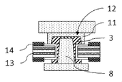
- the groove portion 12 for applying the thermal paste 3 is provided on the base member protruding portion 2.
- the thermal paste 3 stored in the groove 12 spreads inside the through hole 9 by being pressed by the cover member protrusion 8, and the base member protrusion 2 and the cover member protrusion 8 are thermally coupled via the thermal paste 3. Will be done.
- the application position and pressing position of the thermal paste 3 are quantified, and the role of suppressing the variation in the thermal paste performance due to individual differences.
- the convex portion (base member protruding portion 2) has a concave portion (groove portion 12) facing the second protruding portion (cover member protruding portion 8).
- the thermal paste 3 is filled between the second protruding portion (cover member protruding portion 8) and the recess (groove portion 12). Thereby, for example, the contact area between the convex portion (base member protruding portion 2) and the thermal paste 3 can be increased.
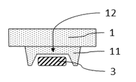
- the groove portion 12 can be formed in the pedestal 11 by eliminating the base member protruding portion 2.
- the first protrusion (pedestal 11) has a recess (groove 12) facing the second protrusion (cover member protrusion 8). This makes it easier to apply the thermal paste 3 to the recess (groove 12) than in the example of FIG.
- the thermal paste 3 is filled between the second protruding portion (cover member protruding portion 8) and the recess (groove portion 12).
- the tip of the second protrusion (cover member protrusion 8) is located inside the recess (groove 12).
- the first protrusion (pedestal 11) closes the through hole 9. As a result, for example, the thermal paste 3 does not easily leak to the surface side of the circuit board 5 on which the heat generating component 4 is mounted.
- the groove portion 12 has a tapered shape so that the pressed thermal paste 3 can easily flow out of the groove portion 12.
- the recess (groove 12) has a taper so that it narrows toward the bottom of the recess (groove 12).
- the embodiment of the present invention may have the following aspects.
- the first and second projecting portions are provided, respectively.
- the circuit board 5 is provided with a through hole 9, and the first and second protrusions are arranged so as to face each other in the through hole 9.
- Thermal paste 3 is applied between the first and second protrusions, and when the housing is assembled, the heat radiation grease is pressed into the through holes 9 by being pressed by the first and second protrusions.
- An electronic control device characterized in that 3 is filled.
- a convex portion or a concave portion is provided at the tip of the first protruding portion and the second protruding portion, and the thermal paste 3 is applied into the concave portion.
- the thermal paste 3 is filled in the through hole 9 by being pressed by the convex portion and the concave portion, and the thermal paste 3 and the circuit board 5 are arranged on substantially the same plane.
- a pedestal 11 is provided between the convex portion and the base member 1 or the cover member 7, or a pedestal 11 for preventing the thermal paste 3 from flowing out is provided in the convex portion of the pedestal 11.
- the circuit board 5 can be sandwiched between the circuit board storage housings without using a board fastener such as a screw 6 (1). ).
- the electronic control device By installing the through hole 9 at the end of the board (the end of the circuit board 5), the circuit board 5 can be sandwiched between the circuit board storage housings without using a board fastener such as a screw 6 (1). ).
- the electronic control device By installing the through hole 9 at the end of the board (the end of the circuit board 5), the circuit board 5 can be sandwiched between the circuit board storage housings without using a board fastener such as a screw 6 (1). ).
- the electronic control device By installing the through hole 9 at the end of the board (the end of the circuit board 5), the circuit board 5 can be sandwiched between the circuit board storage housings without using a board fastener such as a screw 6 (1). ).
- the electronic control device By installing the through hole 9 at the end of the board (the end of the circuit board 5), the circuit board 5 can be sandwiched between
Landscapes
- Cooling Or The Like Of Electrical Apparatus (AREA)
- Cooling Or The Like Of Semiconductors Or Solid State Devices (AREA)
Abstract
Description
図1は、本実施形態に係る放熱構造の構成図の例である。電子制御装置100は、ベース部材1とカバー部材7との間に回路基板5を挟んだ構成になっており、回路基板5は、ネジ6などの締結具でベース部材1に固定されている。ベース部材1からはベース部材突出部2、カバー部材7からはカバー部材突出部8がそれぞれ向かい合うように延伸している。また回路基板5には貫通孔9が設けられており、対向して配置されているベース部材突出部2とカバー部材突出部8が同時に挿通される位置に配置されている。
図3は、実施形態1の構成に加えて、ベース部材突出部2に放熱グリス3を塗布する為の溝部12を設けている。溝部12に溜められた放熱グリス3はカバー部材突出部8により押圧されることで貫通孔9の内側に広がり、ベース部材突出部2とカバー部材突出部8は放熱グリス3を介し熱的に結合される。
また図8のように、ベース部材突出部2を無くし台座11に溝部12を作ることもできる。換言すれば、図7に示すように、第1突出部(台座11)は、第2突出部(カバー部材突出部8)と対向する凹部(溝部12)を有する。これにより、放熱グリス3の凹部(溝部12)への塗布が図6の例よりも容易となる。放熱グリス3は、第2突出部(カバー部材突出部8)と凹部(溝部12)との間に充填される。第2突出部(カバー部材突出部8)の先端は、凹部(溝部12)の内部に位置する。第1突出部(台座11)は、貫通孔9を塞ぐ。これにより、例えば、放熱グリス3は発熱部品4を搭載する回路基板5の面側にもれ出しにくい。
1…ベース部材
2…ベース部材突出部
3…放熱グリス
4…発熱部品
5…回路基板
6…ネジ
7…カバー部材
8…カバー部材突出部
9…貫通孔
10…メッキ
10E…メッキの端部
11…台座
12…溝部
13…GNDパターン
14…レジスト
Claims (13)
- 発熱部品が搭載され、貫通孔を有する回路基板と、
前記貫通孔に向かって突出する第1突出部を有する第1筐体と、
前記第1突出部と対向する第2突出部を有する第2筐体と、
前記貫通孔を形成する前記回路基板の内壁から前記第1突出部及び前記第2突出部へ熱を伝導する放熱グリスと、
を備えることを特徴とする電子制御装置。 - 請求項1に記載の電子制御装置であって、
前記第1突出部は、
前記第2突出部と対向する凸部を有し、
前記放熱グリスは、
前記貫通孔を形成する前記回路基板の内壁と、前記凸部及び前記第2突出部との間に充填される
ことを特徴とする電子制御装置。 - 請求項2に記載の電子制御装置であって、
前記凸部は、
前記第2突出部と対向する凹部を有し、
前記放熱グリスは、
前記第2突出部と前記凹部との間に充填される
ことを特徴とする電子制御装置。 - 請求項3に記載の電子制御装置であって、
前記凹部は、
底に向かうにつれて狭くなるようにテーパーを有する
ことを特徴とする電子制御装置。 - 請求項4に記載の電子制御装置であって、
前記凸部の先端は、
前記貫通孔の内部に位置し、
前記第1突出部は、
前記貫通孔を塞ぐ
ことを特徴とする電子制御装置。 - 請求項5に記載の電子制御装置であって、
前記凸部は、
先細り形状である
ことを特徴とする電子制御装置。 - 請求項6に記載の電子制御装置であって、
前記第2突出部は、
先細り形状である
ことを特徴とする電子制御装置。 - 請求項1に記載の電子制御装置であって、
前記第1突出部は、
前記第2突出部と対向する凹部を有し、
前記放熱グリスは、
前記第2突出部と前記凹部との間に充填される
ことを特徴とする電子制御装置。 - 請求項8に記載の電子制御装置であって、
前記第2突出部の先端は、
前記凹部の内部に位置し、
前記第1突出部は、
前記貫通孔を塞ぐ
ことを特徴とする電子制御装置。 - 請求項1に記載の電子制御装置であって、
前記回路基板は、
GNDパターンを有し、
前記貫通孔は、
前記GNDパターンと接続されたメッキを有し、
前記第1突出部は、
前記メッキに接する
ことを特徴とする電子制御装置。 - 請求項1に記載の電子制御装置であって、
前記貫通孔は、
前記発熱部品の角に隣接し、
前記発熱部品を搭載する回路基板の面に対し、円状に形成される
ことを特徴とする電子制御装置。 - 請求項1に記載の電子制御装置であって、
前記貫通孔は、
前記発熱部品の角に隣接し、
前記発熱部品を搭載する回路基板の面に対し、L字状に形成される
ことを特徴とする電子制御装置。 - 請求項1に記載の電子制御装置であって、
前記貫通孔は、
前記回路基板の縁に隣接し、
前記発熱部品を搭載する回路基板の面に対し、直線状に形成される
ことを特徴とする電子制御装置。
Priority Applications (2)
| Application Number | Priority Date | Filing Date | Title |
|---|---|---|---|
| CN202180081516.1A CN116583944A (zh) | 2020-12-25 | 2021-08-31 | 电子控制装置 |
| JP2022571044A JP7502470B2 (ja) | 2020-12-25 | 2021-08-31 | 電子制御装置 |
Applications Claiming Priority (2)
| Application Number | Priority Date | Filing Date | Title |
|---|---|---|---|
| JP2020216954 | 2020-12-25 | ||
| JP2020-216954 | 2020-12-25 |
Publications (1)
| Publication Number | Publication Date |
|---|---|
| WO2022137653A1 true WO2022137653A1 (ja) | 2022-06-30 |
Family
ID=82158934
Family Applications (1)
| Application Number | Title | Priority Date | Filing Date |
|---|---|---|---|
| PCT/JP2021/031897 Ceased WO2022137653A1 (ja) | 2020-12-25 | 2021-08-31 | 電子制御装置 |
Country Status (3)
| Country | Link |
|---|---|
| JP (1) | JP7502470B2 (ja) |
| CN (1) | CN116583944A (ja) |
| WO (1) | WO2022137653A1 (ja) |
Cited By (1)
| Publication number | Priority date | Publication date | Assignee | Title |
|---|---|---|---|---|
| WO2025263110A1 (ja) * | 2024-06-17 | 2025-12-26 | アルプスアルパイン株式会社 | 電子回路および電子回路の製造方法 |
Families Citing this family (1)
| Publication number | Priority date | Publication date | Assignee | Title |
|---|---|---|---|---|
| US20260173249A1 (en) * | 2024-12-16 | 2026-06-18 | SK Hynix NAND Product Solutions Corp. (dba Solidigm) | Thermal connections within a device enclosure to improve thermal dissipation |
Citations (3)
| Publication number | Priority date | Publication date | Assignee | Title |
|---|---|---|---|---|
| JP2009182182A (ja) * | 2008-01-31 | 2009-08-13 | Nippon Seiki Co Ltd | 電子部品収容ケース体における放熱構造 |
| JP2018006413A (ja) * | 2016-06-28 | 2018-01-11 | 株式会社デンソー | 電子装置、及び、電子装置の製造方法 |
| JP2018064120A (ja) * | 2017-12-25 | 2018-04-19 | 日立オートモティブシステムズ株式会社 | 電子制御装置 |
-
2021
- 2021-08-31 CN CN202180081516.1A patent/CN116583944A/zh active Pending
- 2021-08-31 JP JP2022571044A patent/JP7502470B2/ja active Active
- 2021-08-31 WO PCT/JP2021/031897 patent/WO2022137653A1/ja not_active Ceased
Patent Citations (3)
| Publication number | Priority date | Publication date | Assignee | Title |
|---|---|---|---|---|
| JP2009182182A (ja) * | 2008-01-31 | 2009-08-13 | Nippon Seiki Co Ltd | 電子部品収容ケース体における放熱構造 |
| JP2018006413A (ja) * | 2016-06-28 | 2018-01-11 | 株式会社デンソー | 電子装置、及び、電子装置の製造方法 |
| JP2018064120A (ja) * | 2017-12-25 | 2018-04-19 | 日立オートモティブシステムズ株式会社 | 電子制御装置 |
Cited By (1)
| Publication number | Priority date | Publication date | Assignee | Title |
|---|---|---|---|---|
| WO2025263110A1 (ja) * | 2024-06-17 | 2025-12-26 | アルプスアルパイン株式会社 | 電子回路および電子回路の製造方法 |
Also Published As
| Publication number | Publication date |
|---|---|
| JP7502470B2 (ja) | 2024-06-18 |
| JPWO2022137653A1 (ja) | 2022-06-30 |
| CN116583944A (zh) | 2023-08-11 |
Similar Documents
| Publication | Publication Date | Title |
|---|---|---|
| EP1544915B1 (en) | Electronic module heat sink mounting arrangement | |
| US7697300B2 (en) | Electronic unit and method for manufacturing an electronic unit | |
| JP4638923B2 (ja) | 制御装置 | |
| JP7023298B2 (ja) | 電力変換装置及び電力変換装置の製造方法 | |
| US20180027646A1 (en) | Circuit assembly, electrical junction box, and manufacturing method for circuit assembly | |
| US20110235278A1 (en) | Circuit module | |
| JP2010056493A (ja) | 電子制御装置 | |
| JP7016054B2 (ja) | 電源装置、前照灯、及び移動体 | |
| CN107112736A (zh) | 电子控制装置 | |
| JP2023552884A (ja) | 電子デバイス | |
| JP2018182147A (ja) | 金属部材付き基板、回路構成体及び電気接続箱 | |
| JP2001332670A (ja) | 半導体装置の実装構造 | |
| WO2014132399A1 (ja) | 放熱構造 | |
| JP2006294754A (ja) | 電子装置の放熱構造 | |
| JP2020087966A (ja) | 半導体モジュールおよびそれを用いた半導体装置 | |
| JP7502470B2 (ja) | 電子制御装置 | |
| JP2009223881A (ja) | 無線通信装置 | |
| JP7223639B2 (ja) | 電子制御装置 | |
| JP2026009345A (ja) | 電子制御装置 | |
| JPH09283886A (ja) | 基板実装方法及び実装基板構造並びに該実装基板構造を用いた電子機器 | |
| JP2017162860A (ja) | 電子制御装置 | |
| JP7712108B2 (ja) | 電子制御装置 | |
| JP2004259948A (ja) | 電子制御装置 | |
| CN116235297A (zh) | 基板单元 | |
| WO2025004321A1 (ja) | 熱伝達部材付き基板、回路体及び電気接続箱 |
Legal Events
| Date | Code | Title | Description |
|---|---|---|---|
| 121 | Ep: the epo has been informed by wipo that ep was designated in this application |
Ref document number: 21909811 Country of ref document: EP Kind code of ref document: A1 |
|
| ENP | Entry into the national phase |
Ref document number: 2022571044 Country of ref document: JP Kind code of ref document: A |
|
| WWE | Wipo information: entry into national phase |
Ref document number: 202180081516.1 Country of ref document: CN |
|
| NENP | Non-entry into the national phase |
Ref country code: DE |
|
| 122 | Ep: pct application non-entry in european phase |
Ref document number: 21909811 Country of ref document: EP Kind code of ref document: A1 |