WO2022131296A1 - Battery monitoring device - Google Patents
Battery monitoring device Download PDFInfo
- Publication number
- WO2022131296A1 WO2022131296A1 PCT/JP2021/046289 JP2021046289W WO2022131296A1 WO 2022131296 A1 WO2022131296 A1 WO 2022131296A1 JP 2021046289 W JP2021046289 W JP 2021046289W WO 2022131296 A1 WO2022131296 A1 WO 2022131296A1
- Authority
- WO
- WIPO (PCT)
- Prior art keywords
- voltage
- range
- unit
- detection
- voltage detection
- Prior art date
Links
- 238000012806 monitoring device Methods 0.000 title claims abstract description 61
- 238000001514 detection method Methods 0.000 claims abstract description 353
- 239000003990 capacitor Substances 0.000 claims description 90
- 230000003321 amplification Effects 0.000 claims description 44
- 238000003199 nucleic acid amplification method Methods 0.000 claims description 44
- 238000005070 sampling Methods 0.000 claims description 27
- 238000012546 transfer Methods 0.000 claims description 25
- 230000004044 response Effects 0.000 claims description 9
- 238000012544 monitoring process Methods 0.000 abstract description 20
- 238000010586 diagram Methods 0.000 description 16
- 238000000034 method Methods 0.000 description 9
- YBIDYTOJOXKBLO-USLOAXSXSA-N (4-nitrophenyl)methyl (5r,6s)-6-[(1r)-1-hydroxyethyl]-3,7-dioxo-1-azabicyclo[3.2.0]heptane-2-carboxylate Chemical compound C([C@@H]1[C@H](C(N11)=O)[C@H](O)C)C(=O)C1C(=O)OCC1=CC=C([N+]([O-])=O)C=C1 YBIDYTOJOXKBLO-USLOAXSXSA-N 0.000 description 8
- 238000006243 chemical reaction Methods 0.000 description 8
- 238000003745 diagnosis Methods 0.000 description 8
- 229920005994 diacetyl cellulose Polymers 0.000 description 7
- 230000000694 effects Effects 0.000 description 7
- 238000004891 communication Methods 0.000 description 6
- 230000008569 process Effects 0.000 description 5
- 238000013139 quantization Methods 0.000 description 4
- 238000012545 processing Methods 0.000 description 3
- HBBGRARXTFLTSG-UHFFFAOYSA-N Lithium ion Chemical compound [Li+] HBBGRARXTFLTSG-UHFFFAOYSA-N 0.000 description 2
- 239000000446 fuel Substances 0.000 description 2
- 230000006872 improvement Effects 0.000 description 2
- 229910001416 lithium ion Inorganic materials 0.000 description 2
- 238000012935 Averaging Methods 0.000 description 1
- 238000013459 approach Methods 0.000 description 1
- 230000005540 biological transmission Effects 0.000 description 1
- 238000012937 correction Methods 0.000 description 1
- 238000013461 design Methods 0.000 description 1
- 230000006866 deterioration Effects 0.000 description 1
- 238000007599 discharging Methods 0.000 description 1
- GELKBWJHTRAYNV-UHFFFAOYSA-K lithium iron phosphate Chemical compound [Li+].[Fe+2].[O-]P([O-])([O-])=O GELKBWJHTRAYNV-UHFFFAOYSA-K 0.000 description 1
- 230000009467 reduction Effects 0.000 description 1
- 230000008685 targeting Effects 0.000 description 1
Images


Classifications
-
- G—PHYSICS
- G01—MEASURING; TESTING
- G01R—MEASURING ELECTRIC VARIABLES; MEASURING MAGNETIC VARIABLES
- G01R31/00—Arrangements for testing electric properties; Arrangements for locating electric faults; Arrangements for electrical testing characterised by what is being tested not provided for elsewhere
- G01R31/36—Arrangements for testing, measuring or monitoring the electrical condition of accumulators or electric batteries, e.g. capacity or state of charge [SoC]
- G01R31/396—Acquisition or processing of data for testing or for monitoring individual cells or groups of cells within a battery
-
- G—PHYSICS
- G01—MEASURING; TESTING
- G01R—MEASURING ELECTRIC VARIABLES; MEASURING MAGNETIC VARIABLES
- G01R31/00—Arrangements for testing electric properties; Arrangements for locating electric faults; Arrangements for electrical testing characterised by what is being tested not provided for elsewhere
- G01R31/36—Arrangements for testing, measuring or monitoring the electrical condition of accumulators or electric batteries, e.g. capacity or state of charge [SoC]
- G01R31/382—Arrangements for monitoring battery or accumulator variables, e.g. SoC
- G01R31/3835—Arrangements for monitoring battery or accumulator variables, e.g. SoC involving only voltage measurements
-
- H—ELECTRICITY
- H01—ELECTRIC ELEMENTS
- H01M—PROCESSES OR MEANS, e.g. BATTERIES, FOR THE DIRECT CONVERSION OF CHEMICAL ENERGY INTO ELECTRICAL ENERGY
- H01M10/00—Secondary cells; Manufacture thereof
- H01M10/42—Methods or arrangements for servicing or maintenance of secondary cells or secondary half-cells
- H01M10/48—Accumulators combined with arrangements for measuring, testing or indicating the condition of cells, e.g. the level or density of the electrolyte
-
- H—ELECTRICITY
- H02—GENERATION; CONVERSION OR DISTRIBUTION OF ELECTRIC POWER
- H02J—CIRCUIT ARRANGEMENTS OR SYSTEMS FOR SUPPLYING OR DISTRIBUTING ELECTRIC POWER; SYSTEMS FOR STORING ELECTRIC ENERGY
- H02J7/00—Circuit arrangements for charging or depolarising batteries or for supplying loads from batteries
- H02J7/0047—Circuit arrangements for charging or depolarising batteries or for supplying loads from batteries with monitoring or indicating devices or circuits
- H02J7/0048—Detection of remaining charge capacity or state of charge [SOC]
-
- H—ELECTRICITY
- H02—GENERATION; CONVERSION OR DISTRIBUTION OF ELECTRIC POWER
- H02J—CIRCUIT ARRANGEMENTS OR SYSTEMS FOR SUPPLYING OR DISTRIBUTING ELECTRIC POWER; SYSTEMS FOR STORING ELECTRIC ENERGY
- H02J7/00—Circuit arrangements for charging or depolarising batteries or for supplying loads from batteries
- H02J7/02—Circuit arrangements for charging or depolarising batteries or for supplying loads from batteries for charging batteries from ac mains by converters
-
- G—PHYSICS
- G01—MEASURING; TESTING
- G01R—MEASURING ELECTRIC VARIABLES; MEASURING MAGNETIC VARIABLES
- G01R19/00—Arrangements for measuring currents or voltages or for indicating presence or sign thereof
- G01R19/165—Indicating that current or voltage is either above or below a predetermined value or within or outside a predetermined range of values
- G01R19/16533—Indicating that current or voltage is either above or below a predetermined value or within or outside a predetermined range of values characterised by the application
- G01R19/16538—Indicating that current or voltage is either above or below a predetermined value or within or outside a predetermined range of values characterised by the application in AC or DC supplies
- G01R19/16542—Indicating that current or voltage is either above or below a predetermined value or within or outside a predetermined range of values characterised by the application in AC or DC supplies for batteries
Definitions
- the present disclosure relates to a battery monitoring device that monitors an assembled battery in which a plurality of battery cells are connected in series.
- the battery monitoring device estimates the SOC of each battery cell, and based on the estimation result, performs various controls related to the battery such as equalization processing.
- the SOC is an index indicating the state of charge of the battery, and is an abbreviation for State Of Charge.
- the battery monitoring device is provided with a voltage detection unit that detects the voltage of each battery cell, and SOC is estimated based on the voltage value detected by the voltage detection unit.
- the voltage detection for estimating the SOC is carried out in a wide range from the voltage when the SOC is considered to be 0% to the voltage when the SOC is considered to be 100%.
- the low accuracy of SOC estimation leads to the occurrence of the following problems. That is, in the battery monitoring device, equalization is performed based on the estimated SOC, and therefore, if the estimation accuracy of the SOC is low, the equalization may not be normally performed. In addition, the lower the SOC estimation accuracy, the more margin must be secured in the safe use area of the battery set to prevent the occurrence of over-discharge and over-charge, and the usable area becomes smaller. Problems such as the need to increase the amount of batteries installed in the vehicle arise.
- An object of the present disclosure is to provide a battery monitoring device capable of improving the accuracy of voltage detection of a battery cell.
- the battery monitoring device is a battery monitoring device that monitors an assembled battery having a configuration in which a plurality of battery cells are connected in series, and includes a range designation unit, a voltage detection unit, and a characteristic setting unit.
- the range designation unit specifies a detection range, which is a range for detecting the voltage of the battery cell.
- the voltage detection unit detects the voltage of the battery cell in the detection range, and inputs the A / D converter that inputs the voltage corresponding to the voltage of the battery cell and the digital signal output from the A / D converter. It also includes a digital filter that functions as a low frequency pass filter.
- the voltage detection unit outputs the output signal of the digital filter as a detection signal indicating the detection result of the voltage of the battery cell.
- the characteristic setting unit sets the characteristics of the digital filter.
- the voltage detection range of the battery cell is desired from a wide range that covers the entire voltage range of the battery cell to a narrow range that is a limited narrow range of the total voltage range.
- the detection range to be detected can be selectively specified.
- a desired characteristic can be selectively set as the characteristic of the digital filter.
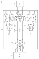
- FIG. 1 is a diagram schematically showing the configuration of the battery monitoring system according to the first embodiment.
- FIG. 2 is a diagram showing a specific first configuration example of the switched capacitor amplifier circuit according to the first embodiment.
- FIG. 3 is a diagram showing a specific second configuration example of the switched capacitor amplifier circuit according to the first embodiment.
- FIG. 4 is for explaining the voltage detection accuracy according to the first embodiment, and is a diagram showing an example of the relationship between the input voltage and the detection error.
- FIG. 5 is a diagram showing an example of the flow of operation by the battery monitoring device according to the first embodiment.
- FIG. 6 is a diagram showing a detection range in the ZOOM operation of each battery cell Cb according to the first specific example of the first embodiment.
- FIG. 7 is for explaining the detection range in the ZOOM operation of each battery cell Cb according to the first specific example of the first embodiment, and is a diagram showing an example of the relationship between the battery voltage and the SOC.
- FIG. 8 is for explaining a method of designating a detection range according to a second specific example of the first embodiment, and is a diagram showing an example of the relationship between OCV and SOC.
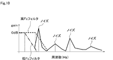
- FIG. 9 is a diagram showing an example of the noise removal performance of the digital filter according to the third specific example of the first embodiment.
- FIG. 10 is a diagram showing an example of various noises generated in the vehicle according to the third specific example of the first embodiment and the noise removal performances of the high Fc filter and the low Fc filter.
- FIG. 11 shows an example of the input / output characteristics of three types of battery cells having different voltage ranges from each other according to the fourth specific example of the first embodiment, and is a diagram showing the relationship between the input / output voltages of the SC amplifier circuit. can be,
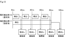
- FIG. 12 is a diagram showing an example of the voltage detection timing of the battery cell by each voltage detection unit according to the fifth specific example of the first embodiment.
- FIG. 13 is a diagram showing an example of the voltage detection timing of the battery cell by each voltage detection unit according to the sixth specific example of the first embodiment.
- FIG. 14 is a diagram schematically showing the configuration of the battery monitoring system according to the second embodiment.
- FIG. 15 is a diagram showing an example of the flow of operation by the battery monitoring device according to the second embodiment.
- FIG. 16 is a diagram showing a specific configuration example of the digital filter according to the second embodiment.
- the battery monitoring system 1 of the present embodiment is mounted on a vehicle such as an automobile, and includes a battery monitoring device 2 and an electronic control device 3.
- the electronic control unit may be abbreviated as ECU.
- the ECU 3 is an example of an external control device.
- the battery monitoring device 2 is a device that detects various states such as the voltage of the assembled battery 4 and monitors the state of the assembled battery 4.
- the battery monitoring device 2 includes a battery monitoring IC 5 which is an integrated circuit in which circuits for performing various operations for battery monitoring are integrated, and a plurality of external elements provided outside the battery monitoring IC 5.
- IC is an abbreviation for Integrated Circuit.
- the assembled battery 4 is mounted on a vehicle such as an automobile, and has a configuration in which a plurality of, for example, 24 battery cells Cb are connected in series between a pair of DC power supply lines L1 and L2.
- the battery cell Cb is, for example, a secondary battery such as a lithium ion battery, a fuel cell, or the like.
- FIG. 1 four battery cells Cb out of the 24 battery cells Cb are shown, and a number is added to the end of the code to distinguish the four battery cells Cb.
- This number corresponds to the arrangement of the battery cells Cb in the assembled battery 4, and 1 is given to the battery cells Cb arranged on the lowest potential side, and 2, 3, 4, and so on toward the high potential side.
- the number given is increasing, and 24 is given to the battery cell Cb arranged on the highest potential side. Therefore, in FIG. 1, the battery cell Cb1 arranged on the lowest potential side, the battery cell Cb2 arranged on the second lowest potential side, and the battery cell Cb23 arranged on the second highest potential side are shown.
- the battery cell Cb24 arranged on the highest potential side is shown.
- Each configuration provided in the battery monitoring device 2 corresponding to each of these four battery cells Cb1, Cb2, Cb23, and Cb24 may be distinguished by adding a similar number to the end of the reference numeral. However, if it is not necessary to distinguish between these configurations, the reference numerals at the end are omitted and they are generically referred to.
- a common mode voltage is superimposed on the battery cell Cb. This common mode voltage becomes higher as the battery cell Cb connected to the upper side of the assembled battery 4, that is, the high potential side, and its maximum value is a relatively high voltage of, for example, about several hundred volts.
- the high potential side terminal of the battery cell Cb24 is connected to the connection terminal PB25 via the resistor RB and also to the connection terminal PS24 via the resistor RS.
- the low-potential side terminal of the battery cell Cb24 and the high-potential side terminal of the battery cell Cb23 are connected to the connection terminal PB24 via the resistor RB and also to the connection terminal PS23 via the resistor RS.
- a capacitor CB is connected between the connection terminal PB25 and the connection terminal PB24.
- a capacitor CS is connected between the connection terminal PS24 and the connection terminal PS23.
- the low-potential side terminal of the battery cell Cb23 and the high-potential side terminal of the battery cell Cb22 (not shown) are connected to the connection terminal PB23 via the resistor RB.
- a capacitor CS is connected between the connection terminal PS23 and the connection terminal PS22 (not shown).
- the high potential side terminal of the battery cell Cb2 is connected to the connection terminal PB3 via the resistor RB and also to the connection terminal PS3 via the resistor RS.
- the low-potential side terminal of the battery cell Cb2 and the high-potential side terminal of the battery cell Cb1 are connected to the connection terminal PB2 via the resistor RB and connected to the connection terminal PS2 via the resistor RS.
- a capacitor CB is connected between the connection terminal PB3 and the connection terminal PB2.
- a capacitor CS is connected between the connection terminal PS3 and the connection terminal PS2.
- the low potential side terminal of the battery cell Cb1 is connected to the connection terminal PB1 via the resistor RB and also to the connection terminal PS1 via the resistor RS.
- a capacitor CB is connected between the connection terminal PB2 and the connection terminal PB1.
- a capacitor CS is connected between the connection terminal PS2 and the connection terminal PS1.
- the filter 6 which is a so-called pie-type low-pass filter is configured by the two resistors RB and the capacitor CB corresponding to each of the battery cells Cb.
- the low-pass filter may be abbreviated as LPF.
- the filter 7, which is a so-called pie-type LPF is configured by the two resistors RS and the capacitor CS corresponding to each of the battery cells Cb. That is, in the above configuration, the filters 6 and 7 are provided so as to correspond to each of the battery cells Cb.
- An equalization switch SW is provided corresponding to each of the plurality of battery cells Cb.
- the equalization switch SW is composed of, for example, a MOS transistor, and constitutes a discharge circuit together with the resistor RB.
- the on / off of the equalization switch is controlled by the control unit 8.
- the control unit 8 controls the overall operation of the battery monitoring IC 5. In the battery equalization process, the operation of each discharge circuit is controlled so that the voltage of each battery cell Cb becomes the same as the voltage of the lowest battery cell Cb.
- the specific connection form of the equalization switch SW is as follows. That is, the equalization switch SW24 corresponding to the battery cell Cb24 is connected between the connection terminal PB25 and the connection terminal PB24.
- the equalization switch SW23 corresponding to the battery cell Cb23 is connected between the connection terminal PB24 and the connection terminal PB23.
- the equalization switch SW2 corresponding to the battery cell Cb2 is connected between the connection terminal PB3 and the connection terminal PB2.
- the equalization switch SW1 corresponding to the battery cell Cb1 is connected between the connection terminal PB2 and the connection terminal PB1.
- the multiplexer 9 inputs each voltage of the connection terminals PB1 to PB25, and selectively selects two voltages required for detecting the voltage of the battery cell Cb to be detected among the input voltages. Output to.
- the multiplexer may be abbreviated as MUX.
- the MUX 9 inputs each voltage of the connection terminals PS1 to PS24, and selectively selects two voltages required for detecting the voltage of the battery cell Cb to be detected among the input voltages. Output to 11.
- the voltage detection unit 10 is a normal system voltage detection unit that mainly performs normal voltage detection, and corresponds to a first voltage detection unit.
- the voltage detection unit 10 detects the voltage of the battery cell Cb in the detection range designated by the control unit 8, and both are switched capacitor amplifier circuits 12 and A / D converters whose operation is controlled by the control unit 8. 13 and a digital filter 14 are provided.
- the switched capacitor may be abbreviated as SC
- the A / D converter may be abbreviated as ADC.
- the SC amplifier circuit 12 inputs the voltage of the battery cell Cb given via the filter 7, MUX9, and the like, and outputs the amplified voltage of the input voltage. In this case, the SC amplifier circuit 12 also performs a level shift to step down the high common mode voltage to the low common mode reference voltage.
- the output voltage of the SC amplifier circuit 12 corresponds to the voltage corresponding to the voltage of the battery cell Cb.
- the ADC 13 inputs the output voltage of the SC amplifier circuit 12 to perform A / D conversion, and outputs a digital signal obtained as a result of the conversion.
- the digital filter 14 functions as an LPF that inputs a digital signal output from the ADC 13 and removes its high frequency component.
- the cutoff frequency, order, and other characteristics of the digital filter 14 are variable, and the settings for these values are made by the control unit 8.
- the voltage detection unit 10 having the above configuration outputs the output signal of the digital filter 14 to the control unit 8 as a detection signal indicating the detection result of the voltage of the battery cell Cb.
- the voltage detection unit 11 is a voltage detection unit of a diagnostic system that mainly performs voltage detection for diagnosis, and corresponds to a second voltage detection unit.
- the voltage detection unit 11 detects the voltage of the battery cell Cb in the detection range designated by the control unit 8, and the SC amplifier circuit 15 having the same configuration as the SC amplifier circuit 12, the ADC 13 and the digital filter 14, respectively. It includes an ADC 16 and a digital filter 17. That is, the voltage detection unit 11 has the same configuration as the voltage detection unit 10.
- the SC amplifier circuit 15 inputs the voltage of the battery cell Cb given via the filter 6 and the MUX 9, and outputs the voltage obtained by amplifying the input voltage.
- the voltage detection unit 11 having the above configuration outputs the output signal of the digital filter 17 to the control unit 8 as a detection signal indicating the detection result of the voltage of the battery cell Cb.
- the control unit 8 is configured as, for example, a logic circuit, and its functional blocks include a detection control unit 21, an equalization control unit 22, a failure diagnosis unit 23, a communication control unit 24, a range specification unit 25, and a characteristic setting unit. It has 26 and so on.
- the control unit 8 communicates with the ECU 3 and executes various controls according to a command or the like given from the ECU 3 via the communication.
- the ECU 3 includes a microcomputer 27, and the microcomputer 27 generates commands for instructing the contents of various controls by the control unit 8.
- the microcomputer may be abbreviated as a microcomputer.
- the detection control unit 21 controls the operation of the voltage detection unit 10 and detects the voltage of the battery cell Cb based on the detection signal output from the digital filter 14 of the voltage detection unit 10. The result of such voltage detection is used for SOC estimation and the like.
- the detection control unit 21 stores data representing the voltage detection result in the register 28. At that time, what kind of detection range the detection result is detected in, in other words, The data is stored in a form that can identify what kind of detection accuracy the data was detected.
- Specific methods for storing such data include a method of adding a flag indicating the detection range, detection accuracy, etc. to the data representing the detection result, and data representing the detection result for each different detection range or for each detection accuracy. A method of dividing the storage location of the data can be mentioned.
- the equalization control unit 22 controls the operation of the equalization switch SW and executes the battery equalization process described above.
- the failure diagnosis unit 23 controls the operation of the voltage detection unit 11 and detects the voltage of the battery cell Cb based on the detection signal output from the voltage detection unit 11.
- the failure diagnosis unit 23 stores data representing the voltage detection result in the register 28.
- the failure diagnosis unit 23 diagnoses failures in various paths and configurations related to voltage detection based on the result of voltage detection by itself and the result of voltage detection by the detection control unit 21.
- the communication control unit 24 controls communication performed with the microcomputer 27 included in the ECU 3 via a communication interface (not shown).
- the range designation unit 25 operates in response to a range designation command given from the ECU 3, and designates a detection range, which is a range for detecting the voltage of the battery cell Cb, for each of the voltage detection units 10 and 11. .. That is, the range designation unit 25 designates the detection range in the voltage detection units 10 and 11 based on the command given from the ECU 3. The range designation unit 25 outputs a signal for designating the detection range to the voltage detection units 10 and 11.
- the characteristic setting unit 26 operates in response to a characteristic setting command given from the ECU 3 via communication, and sets the characteristics of the digital filters 14 and 17. That is, the characteristic setting unit 26 sets the characteristics of the digital filters 14 and 17 based on the command given from the ECU 3.
- the characteristic setting unit 26 outputs a signal for setting the characteristics of the digital filters 14 and 17 to the voltage detection units 10 and 11.
- the SC amplifier circuits 12 and 15 include a sampling capacity and a feedback capacity, sample the voltage of the battery cell Cb by the sampling capacity, and transfer the sampled charge through the feedback capacity to transfer the sampled charge of the battery cell Cb. It outputs a voltage corresponding to the voltage, and has a configuration in which the amplification factor and the offset can be switched.
- the voltage detection units 10 and 11 detect the voltage of the battery cell Cb in the detection range specified by the range specification unit 25 by switching one or both of the amplification factors and the offsets of the SC amplification circuits 12 and 15. ing. In other words, the voltage detection units 10 and 11 are configured to be able to switch the detection range by switching one or both of the amplification factors and offsets of the SC amplification circuits 12 and 15.
- Specific configurations of the SC amplifier circuit 12 include the configuration of the SC amplifier circuit shown in FIG. 1 of JP-A-2019-32175 and SC amplification shown in FIG. 14 of JP-A-2019-32175.
- a circuit configuration or the like can be adopted.
- the former will be referred to as a first configuration example, and the latter will be described as a second configuration example.
- the configuration of the SC amplifier circuit 12 is illustrated here, the same configuration can be adopted for the SC amplifier circuit 15.
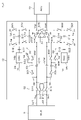
- the SC amplifier circuit 12 of the first configuration example includes an OP amplifier 31 of a differential output type, capacitors C11 to C18, and switches S11 to S25. There is. A voltage output from the MUX 9 through the first output line Lo1 and a voltage output through the second output line Lo2 are input to the SC amplifier circuit 12.
- these two voltages will be referred to as input voltages Vip and Vim.
- the SC amplifier circuit 12 samples the input voltages Vip and Vim by the capacitors C11 and C12 that function as the sampling capacitance, and transfers the sampled charges via the capacitors C13 to C16 that function as the feedback capacitance to input the input.
- This is a sample hold circuit having a differential configuration that outputs a detection voltage corresponding to the voltages Vip and Vim.
- the SC amplifier circuit 12 also performs a level shift to step down the high common mode voltage to the low common mode reference voltage Vcm.
- the common voltage of the OP amplifier 31 is set to be equal to the reference voltage Vcm which is the reference for voltage detection.
- the reference voltage Vcm is an intermediate voltage of the power supply voltage of each circuit included in the battery monitoring IC 5.
- the power supply voltage is, for example, + 5V
- the intermediate voltage is, for example, + 2.5V.
- the OP amplifier 31 outputs output voltages Vop and Vom from its inverting output terminal and non-inverting output terminal, respectively.
- a switch S25 is connected between the inverting output terminal and the non-inverting output terminal of the OP amplifier 31.
- the output voltages Vop and Vom correspond to the detection voltage corresponding to the input voltages Vip and Vim, that is, the voltage corresponding to the voltage of the battery cell Cb, and are converted into digital data by the ADC 13 of the differential input format in the subsequent stage. ..
- the SC amplifier circuit 12 has a configuration capable of imparting an offset so that the output voltages Vop and Vom fall within the input voltage range of the ADC 13.
- the input voltage range of the ADC 13 is, for example, + 2.5V to ⁇ 2.5V.
- the paired capacitors C11 and C12 in the differential configuration have the same capacitance value Cs.
- the "same capacity value" in the present specification is not only the one in which the capacity values are completely the same, but also the ones having the desired effect, there is a slight difference in the capacity values between them, and strictly speaking. Including things that do not match.
- One terminal of the capacitor C11 is connected to the first output line Lo1 via the switch S11 and is connected to the second output line Lo2 via the switch S12.
- One terminal of the capacitor C12 is connected to the second output line Lo2 via the switch S13 and is connected to the first output line Lo1 via the switch S14.
- the switches S11 to S14 constitute a transfer number switching unit 32 for switching the charge transfer number.
- the amplification factor of the SC amplifier circuit 12 changes according to the number of charge transfers. Therefore, in the present embodiment, the SC amplifier circuit 12 is configured such that the amplification factor is switched by switching the number of transfers by the transfer count switching unit 32. That is, in this case, it can be said that the voltage detection unit 10 is configured to switch the amplification factor of the SC amplifier circuit 12 by switching the number of transfers by the transfer number switching unit 32.
- the other terminal of the capacitor C11 is connected to the non-inverting input terminal of the OP amplifier 31, and is also connected to the ground line Lg to which the reference potential of the circuit is given via the switch S15.
- the other terminal of the capacitor C12 is connected to the inverting input terminal of the OP amplifier 31, and is also connected to the ground line Lg via the switch S16.
- the paired capacitors C13 and C14 in the differential configuration have the same capacitance value Cf. Further, the capacitors C15 and C16 that are paired in the differential configuration have the same capacitance value Cf2.
- the capacitor C13 is connected between the non-inverting input terminal and the inverting output terminal of the OP amplifier 31.
- the capacitor C14 is connected between the inverting input terminal and the non-inverting output terminal of the OP amplifier 31.
- One terminal of the capacitor C15 is connected to the non-inverting input terminal of the OP amplifier 31 via the switch S17, and is connected to the ground line Lg via the switch S18.
- the other terminal of the capacitor C15 is connected to the inverting output terminal of the OP amplifier 31 via the switch S19, and is also connected to the ground line Lg via the switch S20.
- One terminal of the capacitor C16 is connected to the inverting input terminal of the OP amplifier 31 via the switch S21 and is connected to the ground line Lg via the switch S22.
- the other terminal of the capacitor C16 is connected to the non-inverting output terminal of the OP amplifier 31 via the switch S23, and is connected to the ground line Lg via the switch S24.
- the capacitor C13 is connected between the non-inverting input terminal and the inverting output terminal of the OP amplifier 31, and the OP amplifier 31 is inverted.
- the capacitor C14 is connected between the input terminal and the non-inverting output terminal.
- the capacitance value of the feedback capacitance is "Cf", which is the capacitance value of the capacitors C13 and C14.
- the capacitors C13 and C15 are connected in parallel between the non-inverting input terminal and the inverting output terminal of the OP amplifier 31, and the inverting input of the OP amplifier 31.
- Capacitors C14 and C16 are connected in parallel between the terminal and the non-inverting output terminal.
- the capacity value of the feedback capacitance is "Cf + Cf2", which is the capacitance value obtained by adding the capacitance values Cf2 of the capacitors C15 and C16 to the capacitance values Cf of the capacitors C13 and C14.
- the capacity value switching unit 33 for switching the capacity value of the feedback capacity is configured by the switches S17, S19, S21, and S23.
- the capacity value switching unit 33 is configured to increase the capacity value of the feedback capacity by switching the switches S17, S19, S21, and S23 from off to on.
- the amplification factor of the SC amplifier circuit 12 changes according to the capacitance value of the feedback capacitance. Therefore, in the present embodiment, the SC amplifier circuit 12 is configured such that the amplification factor is switched by switching the capacitance value by the capacitance value switching unit 33. That is, in this case, it can be said that the voltage detection unit 10 is configured to switch the amplification factor of the SC amplifier circuit 12 by switching the capacity value by the capacity value switching unit 33.
- the capacitors C17 and C18 paired in the differential configuration and the switches S25 to S30 are configured to give the above-mentioned offset.
- One terminal of the capacitor C17 is connected to one terminal of the capacitor C15 and is connected to the non-inverting input terminal of the OP amplifier 31.
- a D / A converter 34 is connected to the other terminal of the capacitor C17.
- the D / A converter may be abbreviated as DAC.
- One terminal of the capacitor C18 is connected to one terminal of the capacitor C16 and is also connected to the inverting input terminal of the OP amplifier 31.
- a DAC35 is connected to the other terminal of the capacitor C18.
- DACs 34 and 35 are capacitive or resistance type DACs that divide and output the input reference voltage Vr, and their internal outputs are voltage Vdp and voltage Vdm. As described above, in the above configuration, the offset of the SC amplifier circuit 12 is switched by the DACs 34 and 35, that is, the offset values Vdp and Vdm are changed.
- the amplification factor of the SC amplifier circuit 12 can be set to an arbitrary value by the combination of the capacitance values Cs, Cf, Cf2, and Cr of the capacitors C11 to C18, that is, the capacitance ratio.
- the capacitance values of the capacitors C11 to C18 are set so that the capacitance ratios of the capacitance values Cs, Cf, Cf2, and Cr are as shown in the following equation (1).
- Cf: Cf2: Cs: Cr 1: 1: 2: 1 ... (1)
- the SC amplifier circuit 12 of the first configuration example described above can execute sampling twice for each voltage detection.
- the input voltage Vip is sampled using the capacitor C11 and the input voltage Vim is sampled using the capacitor C12.
- the input voltage Vip is sampled using the capacitor C12 and the input voltage Vim is sampled using the capacitor C11.
- the operation of the voltage detection unit 10 when the SC amplifier circuit 12 of the first configuration example described above is applied is performed in the order of first sampling ⁇ first charge transfer ⁇ second sampling ⁇ second charge transfer.
- the control unit 8 executes digital processing, which is a process using digital data obtained by A / D converting the output voltages Vop and Vom output from the voltage detection unit 10, so that the voltage of the battery cell Cb Is detected.
- the ON / OFF states of the switches S11 to S30 are as follows. S11: ON, S12: OFF, S13: ON, S14: OFF, S15: ON, S16: ON S17: OFF, S18: ON, S19: OFF, S20: ON S21: OFF, S22: ON, S23: OFF, S24: ON, S25: ON
- the capacitor C11 is charged by the input voltage Vip, and the capacitor C12 is charged by the input voltage Vim. That is, the input voltage Vip is sampled by the capacitor C11, and the input voltage Vim is sampled by the capacitor C12. Further, in the capacitors C13 to C16, all the accumulated charges are discharged by short-circuiting between the terminals thereof. Further, the capacitors C17 and C18 are charged by the reference voltage Vcm.
- the switches S11 to S30 are turned on and off in the following states.
- Vo [1] (2 ⁇ Cs ⁇ Vin-Cr ⁇ Vd) / Cf... (2)
- the ADC 13 inputs the output voltages Vo and Vom obtained by the first charge transfer, performs A / D conversion, and outputs digital data corresponding to the voltage Vo [1], which is the difference voltage between them, to the control unit 8. ..
- the ON / OFF states of the switches S11 to S30 are as follows. S11: OFF, S12: ON, S13: OFF, S14: ON, S15: ON, S16: ON S17: OFF, S18: ON, S19: OFF, S20: ON S21: OFF, S22: ON, S23: OFF, S24: ON, S25: ON
- the capacitor C11 is charged by the input voltage Vim, and the capacitor C12 is charged by the input voltage Vip. That is, the input voltage Vim is sampled by the capacitor C11, and the input voltage Vip is sampled by the capacitor C12.
- the input to the SC amplifier circuit 12 is inverted with respect to the first sampling. Further, in the capacitors C13 to C16, all the accumulated charges are discharged by short-circuiting between the terminals thereof. Further, the capacitors C17 and C18 are charged by the reference voltage Vcm.
- the switches S11 to S30 are turned on and off in the following states.
- Vo [2] ((2, Cs, Vin-Cr, Vd) / Cf) ... (4)
- the following equation (5) can be derived from the above equation (4).
- Vo [2] -4 ⁇ Vin-Vd... (5)
- the voltage Vo [2] is four times the input voltage. That is, the amplification factor in one sampling, that is, the second sampling and the second charge transfer is "4".
- the ADC 13 inputs the output voltages Vo and Vom obtained by the second charge transfer, performs A / D conversion, and outputs digital data corresponding to the voltage Vo [2], which is the difference voltage between them, to the control unit 8. ..
- the control unit 8 executes a process for obtaining the detected value Vad of the voltage of the battery cell Cb, that is, an operation, using the digital data corresponding to each of the voltage Vo [1] and the voltage Vo [2].
- the detected value Vad obtained by such processing is expressed by the following equation (6).
- a voltage 8 times the input voltage is obtained as the detected value Vad of the voltage of the battery cell Cb. That is, the total amplification factor in this case is "8".
- the SC amplification circuit 12 of the second configuration example has capacitors C31 and C32 with respect to the SC amplification circuit 12 of the first configuration example shown in FIG. And the point that switches S31 to S36 are added is different.
- Capacitors C31 and C32 are paired in a differential configuration and have the same capacitance value Csi.
- One terminal of the capacitor C31 is connected to one terminal of the capacitor C11 via the switch S31, and the other terminal is connected to the other terminal of the capacitor C11 via the switch S32. Further, the other terminal of the capacitor C31 is connected to the ground wire Lg via the switch S33.
- One terminal of the capacitor C32 is connected to one terminal of the capacitor C12 via the switch S34, and the other terminal is connected to the other terminal of the capacitor C12 via the switch S35. Further, the other terminal of the capacitor C32 is connected to the ground wire Lg via the switch S36.
- the switches S33 and S36 are turned ON / OFF in the same manner as the switches S15 and S16.
- the switches S31, S32, S34, and S35 are turned ON / OFF according to the switching of the capacity value of the sampling capacity as described later.
- the capacitors C11 and C12 function as sampling capacities and the parallel combined capacities of the capacitors C11 and C31 according to the ON / OFF of the switches S31, S32, S34 and S35. And the state in which the parallel combined capacitance of the capacitors C12 and C32 functions as the sampling capacitance is switched.
- the capacitance value switching unit 36 for switching the capacitance value of the sampling capacitance is configured by the switches S31, S32, S34, and S35. In this case, the capacitance value switching unit 36 increases the sampling capacitance by switching the switches S31, S32, S34, and S35 from off to on.
- the amplification factor of the SC amplifier circuit 12 changes depending not only on the capacity value of the feedback capacity but also on the capacity value of the sampling capacity. Therefore, in the present embodiment, the amplification factor of the SC amplifier circuit 12 is switched not only by the capacity value switching unit 33 but also by the capacity value switching unit 36. It is configured to be. That is, the SC amplifier circuit 12 of the second configuration example includes the capacitance value switching units 33 and 36 for switching both the capacitance value of the sampling capacitance and the capacitance value of the feedback capacitance, and each capacitance value by the capacitance value switching units 33 and 36. The amplification factor is switched by switching between.
- the detection range can be switched by switching the amplification factors of the SC amplification circuits 12 and 15.
- the amplification factor of the SC amplification circuits 12 and 15 is "1"
- the detection range of the voltage detection units 10 and 11 is a relatively wide detection range equivalent to that of the conventional battery monitoring device, and the amplification factor exceeds "1".
- the detection range is limited and narrow within the detection range of the conventional battery monitoring device.
- the operation in the state where the amplification factor is "1” will be referred to as a normal operation
- the operation in the state where the amplification factor is "a value exceeding 1” will be referred to as a ZOOM operation.
- the detection range in normal operation is referred to as a wide range
- the detection range in ZOOM operation is referred to as a narrow range.
- the voltage detection value Vad in normal operation is expressed by the following equation (7).
- the error of the reference voltage Vr of the DACs 34 and 35 is ⁇ Vr
- the quantization error which is the error of the ADC is Vq.
- the voltage detection value Bad / Gaind when the voltage value near “Vr / 2” is detected by subtracting the offset Vr / 2 by the ZOOM operation is expressed by the following equation (8).
- the amplification factor in the analog circuit is Gaina
- the amplification factor in the digital circuit is Gaind.
- the error related to the voltage detection includes an error due to the quantization error Vq and an error due to the error ⁇ Vr of the reference voltage Vr.
- the error due to the error ⁇ Vr of the reference voltage Vr is a constant value regardless of the amplification factor, so that there is no great difference between the case of normal operation and the case of ZOOM operation.
- the error due to the quantization error Vq approaches zero as the amplification factor Gaind is increased in the case of ZOOM operation. Therefore, in the ZOOM operation, it is possible to reduce the error caused by the quantization error Vq as the amplification factor is increased and the detection range is narrowed, and as a result, high accuracy can be realized. In this way, according to the ZOOM operation, it is possible to reduce the temperature characteristics and durability fluctuations related to linear error, thermal noise, ADC error such as flicker, reference voltage Vr error ⁇ Vr, etc., and high accuracy is realized. can do.
- a gain error of "Gaina / Gaind” is included. Since this gain error can be set to zero if Gaina and Gaind have the same value, the circuit design is performed so that they have the same value, but it is difficult to actually match them exactly. .. Therefore, in the present embodiment, the correction is made so that the “Gaina / Gaind” term becomes “1”, whereby the gain error is set to zero.
- FIG. 4 shows an example of the relationship between the input voltage Vin and the detection error when the error ⁇ Vr of the reference voltage Vr is 1 mV, the error of the ADC is 0.5 mV, and the amplification factor is “8”. ..
- the detection range in normal operation is 0 to 5V
- the detection range in ZOOM operation is 2.25 to 2.75V.
- the minus side error in the normal operation is marked with a black circle
- the plus side error in the normal operation is marked with an X mark
- the minus side error in the ZOOM operation is marked with a white circle. Is attached, and a black triangle mark is attached to the error on the plus side in the ZOOM operation.
- the detection error with respect to the ideal value is a very small value as compared with the case of the normal operation.
- the voltage detection accuracy in the ZOOM operation is greatly improved as compared with the voltage detection accuracy in the normal operation.
- the voltage detection accuracy in the ZOOM operation increases as the amplification factor increases. Therefore, in the configuration of the present embodiment, the wider the detection range of the voltage detection units 10 and 11, the lower the voltage detection accuracy, and the narrower the detection range, the higher the detection accuracy.
- the battery monitoring device 2 having the above configuration executes various operations based on a command given from the ECU 3.
- the "cell detection command” is transmitted from the ECU 3.
- the "cell detection command” is a command for instructing voltage detection in normal operation, and includes a range specification command for designating a wide range of detection and a characteristic setting command for setting the characteristics of the digital filters 14 and 17 to predetermined characteristics. ..
- the characteristic setting command does not have to be included in the "cell detection command", and may be transmitted in advance as a command different from the "cell detection command”.
- the battery monitoring device 2 When the battery monitoring device 2 receives the "cell detection command”, it executes "cell detection”. In “cell detection”, the detection range and the characteristics of the digital filters 14 and 17 are set based on the “cell detection command”, and an operation for detecting the voltage of the battery cell Cb is performed. Subsequently, a "read command” is transmitted from the ECU 3.
- the "read command” is a command for commanding reading of the result of voltage detection in a wide range.
- the battery monitoring device 2 executes the "read”. In “reading”, data representing the result of voltage detection in a wide range is read from the register 28, and an operation for transmitting the data to the ECU 3 is performed.
- the "ZOOM command” is transmitted from the ECU 3.
- the "ZOOM command” is a command for instructing voltage detection in ZOOM operation, and includes a range specification command for designating a narrow detection range and a characteristic setting command for setting the characteristics of the digital filters 14 and 17 to predetermined characteristics. ..
- the characteristic setting command does not have to be included in the "ZOOM command", and may be transmitted in advance as a command different from the "ZOOM command".
- the battery monitoring device 2 When the battery monitoring device 2 receives the "ZOOM command”, it executes "ZOOM detection". In “ZOOM detection”, the detection range and the characteristics of the digital filters 14 and 17 are set based on the "ZOOM command”, and an operation for detecting the voltage of the battery cell Cb is performed. Subsequently, the ECU 3 transmits a "ZOOM read command".
- the "ZOOM read command” is a command for instructing to read the result of voltage detection in a narrow range.
- the battery monitoring device 2 Upon receiving the "ZOOM read command", the battery monitoring device 2 executes the "ZOOM read”. In “ZOOM reading”, data representing the result of voltage detection in a narrow range is read from the register 28, and an operation for transmitting the data to the ECU 3 is performed.
- the battery monitoring device 2 of the present embodiment can switch the detection range which is the range for detecting the voltage of the battery cell Cb, and eventually the detection accuracy of the voltage of the battery cell Cb. It can be done based on various ideas. Hereinafter, a plurality of specific examples of such switching will be described.
- the battery monitoring device 2 individually designates a detection range in the ZOOM operation for each battery cell Cb. That is, in this case, the range designation unit 25 is configured so that the detection range can be independently designated for each battery cell Cb. In this case, first, the voltage level of each battery cell Cb is searched. Such a search can be performed, for example, by performing voltage detection in normal operation.
- the detection range in the ZOOM operation of each battery cell Cb is individually specified.
- the detection range in the ZOOM operation is 0 to 0.5V, 0.5 to 1.0V, ..., 4.0 to 4.5V, 4.5 to 5.0V.
- the range of 0 to 5.0V is divided into 0.5V increments.
- Such selection of the detection range can be performed by switching the offsets of the SC amplifier circuits 12 and 15.
- the voltage value of the battery cell Cb1 was in the range of 3.0 to 3.5V, and the voltage values of the battery cells Cb2 to Cb24 were 3.5 to 4. It is assumed that the voltage is in the range of 0V.
- the detection range in the ZOOM operation of the battery cell Cb1 is set to the range of 3.0 to 3.5V, and the detection range in the ZOOM operation of the battery cells Cb2 to Cb24 is set. It is set in the range of 3.5 to 4.0V. After that, voltage detection in the ZOOM operation is performed based on the detection range set in this way.
- the battery monitoring device 2 specifies a detection range based on a cell voltage range predetermined for each type of battery cell Cb. That is, in this case, the range specifying unit 25 specifies the detection range based on the cell voltage range.
- a detection range can be specified in consideration of the following points. That is, in the battery monitoring device 2, it is necessary to improve the estimation accuracy of the SOC in the region where the SOC is close to 0% and the region where the SOC is close to 100%. This is because if the SOC estimation accuracy is lowered in these regions, over-discharging or over-charging may occur.
- a narrow range is specified as the detection range in the region where the SOC is close to 0% and the region where the SOC is close to 100%, and as the detection range in the other regions. It is designed to specify a wide range.
- the digital filters 14 and 17 have different noise removal performance depending on the cutoff frequency Fc.
- the characteristic with a cutoff frequency of 26 Hz is Fc1
- the characteristic with a cutoff frequency of 422 Hz is Fc2
- the characteristic with a cutoff frequency of 1 kHz is Fc3
- the characteristic with a cutoff frequency of 2 kHz is Fc4
- the cutoff frequency is The characteristic of 3 kHz is Fc5
- the characteristic of cutoff frequency is Fc6
- the characteristic of cutoff frequency of 14 kHz is Fc7
- the characteristic of cutoff frequency is 27 kHz is Fc8.
- the noise generated in the vehicle contains various frequency components.
- a high Fc filter which is a filter with a relatively high cutoff frequency Fc, may not be able to completely remove the noise having a lower frequency among these noises.
- the low Fc filter which is a filter having a relatively low cutoff frequency Fc, it is possible to almost certainly remove noise having a low frequency.
- the digital filters 14 and 17 can remove noise at a lower frequency as the cutoff frequency Fc is lowered, that is, the heavier the filter, but the delay time in the filter becomes longer by that amount. That is, the conversion time becomes long.
- the digital filters 14 and 17 the higher the cutoff frequency Fc, that is, the lighter the filter, the more difficult it is to remove noise at a lower frequency, but the shorter the delay time in the filter, that is, the conversion. The time will be shorter.
- the battery monitoring device 2 has a relatively high cutoff frequency of the digital filters 14 and 17 when a wide range, which is a relatively wide range, is specified as the detection range.
- the cutoff frequency of the digital filters 14 and 17 should be set to a low frequency, which is a relatively low frequency. It has become.
- the characteristic setting unit 26 sets the cutoff frequency, which is a characteristic of the digital filters 14 and 17, to a high frequency. Further, in this case, when the range specifying unit 25 specifies a narrow range as the detection range, the characteristic setting unit 26 sets the cutoff frequency, which is a characteristic of the digital filters 14 and 17, to a low frequency. .. By doing so, the conversion time is shortened when the voltage is detected in a wide range, so that the detection time can be further shortened, and the noise removal performance is improved when the voltage is detected in a narrow range, which is high. Further improvement in accuracy can be achieved.
- the battery monitoring device 2 switches the detection range according to the type of the battery cell Cb. That is, in this case, the range designation unit designates the detection range based on the type of the battery cell Cb.
- the voltage range of the battery cell Cb is different depending on the type of, for example, a lithium ion battery, a fuel cell, and the like. Therefore, in the fourth specific example, the battery monitoring device 2 switches the detection range so that the voltage can be detected in the entire voltage range of the battery cell Cb to be detected. Such switching of the detection range can be performed as follows.
- the relationship between the input voltage Vin and the output voltage Vo of the SC amplifier circuits 12 and 15 is expressed by the following equation (9).
- Vo (Cs ⁇ Vin) / Cf- (Cr ⁇ Vr) / Cf... (9)
- the detection range is changed by changing the capacitance ratio, the value of the reference voltage Vr, etc., in other words, by changing the amplification factor and the offset in the SC amplifier circuits 12 and 15. Can be adjusted to the desired range, that is, the detection range can be switched to an appropriate range.
- FIG. 11 shows the input / output characteristics of three types of battery cells Cb having different voltage ranges from each other.
- A, B, and C are added to the end of each of the three battery cells Cb in order to distinguish them.
- the detection range is switched so that the output voltage Vo of the SC amplifier circuits 12 and 15 falls within the input voltage range of the ADCs 13 and 16 for each of the three types of battery cells Cb. This enables voltage detection in the entire voltage range for each of the three types of battery cells Cb.
- the battery monitoring device 2 specifies that the detection ranges of the voltage detection units 10 and 11 are the same as each other, and the voltage detection units 10 and 11 include the battery monitoring device 2.
- the characteristics of the digital filters 14 and 17 are set to be the same as each other. That is, in this case, the range designation unit 25 designates each detection range so that the detection range in the voltage detection unit 10 and the detection range in the voltage detection unit 11 are the same range. Specifically, the range designation unit 25 designates a wide range or a narrow range as each detection range in the voltage detection units 10 and 11.
- the characteristic setting unit 26 sets each characteristic so that the characteristics of the digital filter 14 included in the voltage detection unit 10 and the characteristics of the digital filter 17 included in the voltage detection unit 11 are the same as each other. There is. Specifically, the characteristic setting unit 26 sets a high frequency or a low frequency as each cutoff frequency of the digital filters 14 and 17.
- the "same timing" in the present specification and the like means not only that the timings are completely the same, but also that the timings are slightly different from each other as long as they have the desired effect. Including things that we haven't done. According to such a fifth specific example, the detection timing by each of the voltage detection units 10 and 11 is as shown in FIG. 12, for example.
- the voltage detection unit 11 also detects the voltage of the battery cell Cb1 while the voltage detection unit 10 detects the voltage of the battery cell Cb1. Similar to the battery cell Cb1, the voltage detection unit 10 and the voltage detection unit 11 detect the voltage of the same battery cell Cb in the same period after the battery cell Cb2. By doing so, the voltage detection timing of each battery cell Cb by the voltage detection units 10 and 11 can be made uniform, and by extension, the voltage acquisition timing and the voltage detection unit 11 of each battery cell Cb using the voltage detection unit 10. The consistency with the acquisition timing of the voltage of each battery cell Cb using the above is improved.
- the consistency between the time constant of the digital filter 14 of the voltage detection unit 10 and the time constant of the digital filter 17 of the voltage detection unit 11 is improved. Therefore, according to the fifth specific example, even when the voltage between the terminals of each battery cell Cb fluctuates greatly, the voltage detection value of the predetermined battery cell Cb by the voltage detection unit 10 and the voltage detection unit It becomes possible to substantially match the detected value of the voltage of the predetermined battery cell Cb according to No. 11, and as a result, the accuracy of failure diagnosis is improved.
- the voltage detection values of the battery cells Cb1 to Cb6 by the voltage detection unit 10 are V1 to V6, and the voltage detection values of the battery cells Cb1 to Cb6 by the voltage detection unit 10 are V1'to V6'. ..
- the battery monitoring device 2 specifies a wide range of detection in the voltage detection unit 10, that is, the voltage detection accuracy of the voltage detection unit 10 is made coarse and the voltage is coarse.
- the detection range in the detection unit 11 is specified in a narrow range, that is, the voltage detection accuracy of the voltage detection unit 11 is made high. That is, in this case, the range specifying unit 25 designates a wide range that is a relatively wide range as the detection range in the voltage detection unit 10, and also specifies a narrow range that is a relatively narrow range as the detection range in the voltage detection unit 11. It is designed to be specified.
- the detection timing by each of the voltage detection units 10 and 11 is as shown in FIG. 13, for example.
- the voltage detection unit 10 executes the voltage detection operation in a relatively short cycle, for example, every 20 ms. Therefore, the detected value of the coarsely accurate voltage detected by the voltage detecting unit 10 is read from the register 28 at a relatively short cycle as in the case of detection.
- the voltage detection unit 11 since the voltage detection unit 11 has a narrow detection range, the voltage detection unit 11 executes a voltage detection operation at a longer cycle than the cycle of the voltage detection unit 10, for example, every 100 ms. Therefore, the detected value of the high-precision voltage detected by the voltage detection unit 11 is read from the register 28 at a relatively long cycle as in the case of detection.
- the voltage detection operations by the voltage detection units 10 and 11 are performed in parallel.
- the voltage detection unit 10 acquires the detection value of the voltage of each battery cell Cb at the same coarse accuracy as the conventional one and the same timing as the conventional one, and the voltage detection unit 11 obtains the detection value. For example, it is possible to acquire the detected value of the voltage of each battery cell Cb detected with higher accuracy than before every relatively long cycle such as every 100 ms. That is, in this case, it is possible to perform highly accurate voltage detection while maintaining the conventional schedule for battery monitoring.
- the battery monitoring device 2 includes a range specifying unit 25 that specifies a detection range that is a range for detecting the voltage of the battery cell Cb, and a characteristic setting unit 26 that sets the characteristics of the digital filters 14 and 17 included in the voltage detecting units 10 and 11. I have.
- the voltage detection range of the battery cell Cb ranges from a wide range that covers the entire voltage range of the battery cell Cb to a narrow range that is a limited narrow range of the total voltage range.
- the desired detection range can be selectively specified.
- desired characteristics can be selectively set as the filter characteristics of the digital filters 14 and 17. By doing so, it is possible to detect the voltage of the battery cell Cb after setting an appropriate detection range and an appropriate filter characteristic according to various conditions. Therefore, according to the present embodiment, the accuracy of voltage detection of the battery cell Cb can be improved.
- the SOC estimation accuracy can be further improved, and the relationship between the SOC and the OCV as in the case of an LFP battery, for example.
- the target is a battery in which the area where the voltage becomes flat is large, the SOC can be estimated with sufficient accuracy for practical use. Therefore, according to the present embodiment, the equalization process can be carried out more reliably and normally.
- the margin secured in the safe use area of the battery set for preventing the occurrence of over-discharge and over-charge is reduced, and the usable area is expanded by that amount, and by extension, the battery. It can be used up, and as a result, the effect of increasing the mileage of the vehicle or reducing the amount of batteries installed in the vehicle can be obtained.
- the range designation unit 25 operates in response to a range designation command given from the external ECU 3, and the characteristic setting unit 26 operates in response to the characteristic setting command given by the ECU 3. That is, both the range specifying unit 25 and the characteristic setting unit 26 are designed to specify the detection range and set the filter characteristics based on the command given from the ECU 3. As described above, in the present embodiment, the detection range is specified and the filter characteristics are set by the combination of the battery monitoring device 2 and the ECU 3, so that, for example, the vehicle is running, the vehicle is stopped, the vehicle is being charged, and the like. It is possible to detect the voltage of the battery cell Cb after setting an appropriate detection range and an appropriate filter characteristic according to each of various driving scenes, and it is possible to realize more accurate battery control.
- the range designation unit 25 can specify a detection range based on a cell voltage range predetermined for each type of battery cell Cb.
- the range designation unit 25 can specify a narrow range as a detection range in a region where the SOC is close to 0% and a region where the SOC is close to 100%, and can specify a wide range as a detection range in other regions. ..
- the accuracy of voltage detection becomes high accuracy, which is relatively high accuracy, and the occurrence of over-discharge and over-charging can be prevented.
- the accuracy of voltage detection becomes coarse, which is relatively low, and the time required for voltage detection, and thus the time required for SOC estimation, can be shortened.
- the characteristic setting unit 26 sets the cutoff frequency, which is a filter characteristic, to a high frequency, which is a relatively high frequency, and ranges.
- the designation unit 25 specifies a narrow range that is a relatively narrow range as the detection range
- the characteristic setting unit 26 sets the cutoff frequency, which is a characteristic of the filter, to a low frequency, which is a relatively low frequency. Can be done.
- the conversion time is shortened when the voltage is detected in a wide range, so that the detection time can be further shortened, and the noise removal performance is improved when the voltage is detected in a narrow range, which is high. Further improvement in accuracy can be achieved.
- the deterioration of the S / N ratio due to the noise is suppressed by detecting the voltage in a narrow range and improving the noise removal performance. As a result, the voltage detection accuracy can be improved.
- the range designation unit 25 can specify each detection range so that the detection range in the voltage detection unit 10 of the normal system and the detection range in the voltage detection unit 11 of the diagnostic system are the same range. Further, the characteristic setting unit 26 sets each characteristic so that the characteristics of the digital filter 14 included in the voltage detection unit 10 of the normal system and the characteristics of the digital filter 17 included in the voltage detection unit 11 of the diagnostic system are the same as each other. Can be done. By doing so, the consistency of the voltage acquisition timing of each battery cell Cb using each of the voltage detection units 10 and 11 is improved, and the time constants of the digital filters 14 and 17 of the voltage detection units 10 and 11 are improved. Consistency is improved.
- the voltage detection unit 10 detects the voltage of the predetermined battery cell Cb and the voltage detection unit 11. It is possible to roughly match the detected value of the voltage of the predetermined battery cell Cb, and as a result, the accuracy of the failure diagnosis is improved. Further, according to the above configuration, when a large noise is generated in the vehicle, if a narrow range is specified as the detection range for both the voltage detection units 10 and 11, the noise removal performance of both the normal system and the diagnostic system can be improved. It can be improved, and as a result, the accuracy of failure diagnosis can be maintained well.
- the range specifying unit 25 designates a wide range that is a relatively wide range as the detection range in the voltage detection unit 10 of the normal system, and also designates a narrow range that is a relatively narrow range as the detection range in the voltage detection unit 11. be able to.
- the voltage detection unit 10 acquires the voltage detection value of each battery cell Cb with the same coarse accuracy as the conventional one and the same timing as the conventional one, and the voltage detection unit 11 makes a comparison, for example, every 100 ms. It is possible to acquire the detected value of the voltage of each battery cell Cb detected with higher accuracy than before every long cycle. That is, according to the above configuration, it is possible to perform highly accurate voltage detection while maintaining the conventional schedule for battery monitoring.
- the voltages of the plurality of battery cells Cb constituting the assembled battery 2 do not completely match, and often have different voltage values. Therefore, the appropriate detection range for each battery cell Cb may not be the same but may be different. Therefore, the range specifying unit 25 can independently specify the detection range for each battery cell Cb. By doing so, it is possible to perform voltage detection after setting an appropriate detection range for each battery cell Cb, and it is possible to further improve the accuracy of voltage detection of each battery cell Cb.
- the range designation unit 25 can specify the detection range based on the type of the battery cell Cb.
- the range specifying unit 25 can switch the detection range so that the output voltage of the SC amplifier circuits 12 and 15 falls within the input voltage range of the ADCs 13 and 16 for each of the plurality of battery cells Cb having different voltage ranges. According to this, voltage detection is possible in the entire voltage range for each of a plurality of types of battery cells Cb.
- the voltage detection units 10 and 11 sample the voltage of the battery cell Cb by the capacitors C11 and C12, transfer the sampled charge through the capacitors C13 to C16, and output the voltage corresponding to the voltage of the battery cell Cb. It is designated by the range specifying unit 25 by providing SC amplification circuits 12 and 15 having a configuration in which the amplification factor and the offset can be switched, and by switching one or both of the amplification factors and the offsets of the SC amplification circuits 12 and 15. The voltage of the battery cell Cb is detected in the detection range. According to such a configuration, the voltage detection accuracy can be improved as the detection range in the voltage detection units 10 and 11 is narrowed.
- the battery monitoring device 42 included in the battery monitoring system 41 of the present embodiment includes the battery monitoring IC 43 instead of the battery monitoring IC 5 with respect to the battery monitoring device 2 of the first embodiment. Is different.
- the battery monitoring IC 43 is different from the battery monitoring IC 5 in that the control unit 44 is provided in place of the control unit 8.
- the control unit 44 has a command generation unit 45 added to the control unit 8, a range specification unit 46 and a characteristic setting unit 47 in place of the range specification unit 25 and the characteristic setting unit 26, and the like. It's different.
- the command generation unit 45 generates a range designation command and a characteristic setting command based on the voltage detection result by one or both of the voltage detection unit 10 and the voltage detection unit 11.
- Each command generated by the command generation unit 45 is the same as each command generated by the ECU 3 in the first embodiment. Therefore, the range designation unit 46 operates by receiving the range designation command generated by the command generation unit 45, and the characteristic setting unit 47 operates by receiving the characteristic setting command generated by the command generation unit 45.
- the control unit 44 of the battery monitoring IC 43 is configured to specify the detection range and set the filter characteristics based on its own judgment instead of the command from the ECU 3.
- control unit 44 performs voltage detection by normal operation with a wide detection range, and then reads the voltage detection result in the wide range and coarse accuracy from the register 28. Then, the control unit 44 determines the required range based on the read voltage detection result, and sets an appropriate detection range and filter characteristics for the ZOOM operation in which the detection range is narrow. After that, the control unit 44 performs voltage detection by ZOOM operation within the detection range and filter characteristics set as described above. Hereinafter, such a series of operations will be referred to as self-propelled operations.
- the characteristics of the filter in the ZOOM operation may be set based on a command from the ECU 3.
- the "self-propelled operation command” is transmitted from the ECU 3.
- the “self-propelled operation command” is a command for instructing the execution of the self-propelled operation.
- the battery monitoring device 42 Upon receiving the "self-propelled operation command", the battery monitoring device 42 starts the self-propelled operation described above. In this case, the self-propelled operation is repeatedly executed. That is, in this case, the battery monitoring device 42 does not require the transmission of a command from the ECU 3, and limits the detection range to voltage detection by normal operation, that is, "cell detection”, which has a wide detection range. Voltage detection by ZOOM operation, that is, "ZOOM detection” is executed alternately and periodically.
- the battery monitoring device 42 executes voltage detection by normal operation and voltage detection by ZOOM operation a predetermined number of times by such self-propelled operation, and when a "read command" is given from the ECU 3, the battery monitoring device 42 detects the voltage a predetermined number of times. The result is read from register 28. In this case, the detection result of the voltage of the predetermined number of times is stored in the register 28 as the value obtained by averaging the detected values of the voltage of the predetermined number of times through the digital filters 14 and 17.
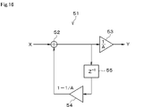
- a primary IIR filter circuit 51 as shown in FIG. 16 can be adopted as a specific configuration of the digital filters 14 and 17.
- IIR is an abbreviation for Infinite Impulse Response.
- the primary IIR filter circuit 51 includes an adder 52, a multiplier 53, 54, and a delayer 55 provided between the input X and the output Y. According to the digital filters 14 and 17 adopting such a configuration, it is possible to output a signal representing a value as if a moving average of the detection results of a predetermined number of times was taken.
- the battery monitoring device 42 of the present embodiment described above can also perform the same operation as the battery monitoring device 42 of the first embodiment. Therefore, the same effect as that of the first embodiment can be obtained by this embodiment as well. Further, according to the present embodiment, the battery monitoring device 42 does not require a command from the ECU 3, and based on its own judgment, appropriately sets the detection range and the filter characteristics in the ZOOM operation according to various situations. Can be set to a value.
- the specific configurations of the SC amplifier circuits 12 and 15 are not limited to those described in each of the above embodiments, and can be appropriately changed as long as the configurations can realize the same functions.
- the battery monitoring device is not limited to the one provided with the voltage detection unit 10 of the normal system and the voltage detection unit 11 of the diagnostic system, and may be configured to include only one voltage detection unit.
Abstract
This battery monitoring device (2, 42) for monitoring an assembled battery (4) having a configuration in which a plurality of battery cells (Cb) are connected in series comprises: a range designation unit (25, 46) which designates a detection range, which is a range for detecting the voltage of the battery cell; an A/D converter (13, 16) which detects the voltage of the battery cell in the detection range and inputs a voltage corresponding to the voltage of the battery cell; a digital filter (14, 17) which receives a digital signal output from the A/D converter and functions as a low-pass filter; a voltage detection unit (10, 11) which outputs an output signal of the digital filter as a detection signal indicating the detection result of the voltage of the battery cell; and a characteristic setting unit (26, 47) which sets the characteristics of the digital filter.
Description
本出願は、2020年12月17日に出願された日本出願番号2020-209289号に基づくもので、ここにその記載内容を援用する。
This application is based on Japanese Application No. 2020-209289 filed on December 17, 2020, and the contents of the description are incorporated herein by reference.
本開示は、複数の電池セルが直列接続された組電池を監視する電池監視装置に関する。
The present disclosure relates to a battery monitoring device that monitors an assembled battery in which a plurality of battery cells are connected in series.
特許文献1に開示されているように、電池監視装置は、各電池セルのSOCを推定し、その推定結果に基づいて均等化処理など電池に関する各種の制御を行っている。なお、SOCは、電池の充電状態を表す指標であり、State Of Chargeの略称である。電池監視装置には、各電池セルの電圧を検出する電圧検出部が設けられており、その電圧検出部により検出された電圧値に基づいてSOCの推定が行われる。SOCの推定のための電圧検出としては、SOCが0%であると考えられるときの電圧からSOCが100%であると考えられるときの電圧にわたる広い領域で実施されるようになっている。
As disclosed in Patent Document 1, the battery monitoring device estimates the SOC of each battery cell, and based on the estimation result, performs various controls related to the battery such as equalization processing. The SOC is an index indicating the state of charge of the battery, and is an abbreviation for State Of Charge. The battery monitoring device is provided with a voltage detection unit that detects the voltage of each battery cell, and SOC is estimated based on the voltage value detected by the voltage detection unit. The voltage detection for estimating the SOC is carried out in a wide range from the voltage when the SOC is considered to be 0% to the voltage when the SOC is considered to be 100%.
従来の電池監視装置では、上述したように広い領域で電池セルの電圧検出を実施していることから電圧の検出精度の高精度化には限界があり、そのため、SOCの推定精度を十分に高めることが困難であった。特に、LFP電池などのようにSOCとOCVとの関係がフラットになる領域が多くなるような電池を対象とした場合には、SOCの推定精度が実用上不十分となる程度まで低下することが懸念される。なお、LFPは、リン酸鉄リチウムの略称であり、OCVは、Open Circuit Voltageの略称である。
In the conventional battery monitoring device, since the voltage detection of the battery cell is performed in a wide range as described above, there is a limit to the high accuracy of the voltage detection accuracy, and therefore, the estimation accuracy of the SOC is sufficiently improved. It was difficult. In particular, when targeting a battery such as an LFP battery in which the relationship between the SOC and the OCV becomes flat in many areas, the estimation accuracy of the SOC may decrease to the extent that it is practically insufficient. I am concerned. LFP is an abbreviation for lithium iron phosphate, and OCV is an abbreviation for Open Circuit Voltage.
SOCの推定精度が低くなるということは、次のような問題の発生に繋がる。すなわち、電池監視装置では、推定されたSOCに基づいて均等化が行われることから、SOCの推定精度が低ければ均等化を正常に実施できなくなるおそれがある。また、SOCの推定精度が低くなればなるほど、過放電および過充電の発生防止のために設定される電池の安全使用領域にマージンを多く確保しなければならなくなり、使用可能領域が少なくなったり、車両に搭載される電池の量を増やさなければならない、といった問題が生じる。
The low accuracy of SOC estimation leads to the occurrence of the following problems. That is, in the battery monitoring device, equalization is performed based on the estimated SOC, and therefore, if the estimation accuracy of the SOC is low, the equalization may not be normally performed. In addition, the lower the SOC estimation accuracy, the more margin must be secured in the safe use area of the battery set to prevent the occurrence of over-discharge and over-charge, and the usable area becomes smaller. Problems such as the need to increase the amount of batteries installed in the vehicle arise.
本開示の目的は、電池セルの電圧検出の精度を向上することができることができる電池監視装置を提供することにある。
An object of the present disclosure is to provide a battery monitoring device capable of improving the accuracy of voltage detection of a battery cell.
本開示の一態様において、電池監視装置は、複数の電池セルが直列接続された構成の組電池を監視する電池監視装置であって、範囲指定部、電圧検出部および特性設定部を備える。範囲指定部は、電池セルの電圧を検出する範囲である検出範囲を指定する。電圧検出部は、検出範囲において電池セルの電圧を検出するものであり、電池セルの電圧に対応した電圧を入力するA/D変換器およびA/D変換器から出力されるデジタル信号を入力するとともに低域通過フィルタとして機能するデジタルフィルタを含む。電圧検出部は、デジタルフィルタの出力信号を電池セルの電圧の検出結果を表す検出信号として出力する。特性設定部は、デジタルフィルタの特性を設定する。
In one aspect of the present disclosure, the battery monitoring device is a battery monitoring device that monitors an assembled battery having a configuration in which a plurality of battery cells are connected in series, and includes a range designation unit, a voltage detection unit, and a characteristic setting unit. The range designation unit specifies a detection range, which is a range for detecting the voltage of the battery cell. The voltage detection unit detects the voltage of the battery cell in the detection range, and inputs the A / D converter that inputs the voltage corresponding to the voltage of the battery cell and the digital signal output from the A / D converter. It also includes a digital filter that functions as a low frequency pass filter. The voltage detection unit outputs the output signal of the digital filter as a detection signal indicating the detection result of the voltage of the battery cell. The characteristic setting unit sets the characteristics of the digital filter.
上記構成によれば、電池セルの電圧の検出範囲として、電池セルの電圧の全電圧範囲に及ぶような広い範囲である広範囲から、全電圧範囲のうち限定した狭い範囲である狭範囲まで、所望する検出範囲を選択的に指定することができる。また、上記構成によれば、デジタルフィルタの特性として、所望する特性を選択的に設定することができる。このようにすれば、様々な条件に応じた適切な検出範囲および適切なデジタルフィルタの特性を設定したうえで、電池セルの電圧を検出することができる。そのため、上記構成によれば、電池セルの電圧検出の精度を向上することができるという優れた効果が得られる。
According to the above configuration, the voltage detection range of the battery cell is desired from a wide range that covers the entire voltage range of the battery cell to a narrow range that is a limited narrow range of the total voltage range. The detection range to be detected can be selectively specified. Further, according to the above configuration, a desired characteristic can be selectively set as the characteristic of the digital filter. By doing so, it is possible to detect the voltage of the battery cell after setting an appropriate detection range and appropriate digital filter characteristics according to various conditions. Therefore, according to the above configuration, it is possible to obtain an excellent effect that the accuracy of voltage detection of the battery cell can be improved.
本開示についての上記目的およびその他の目的、特徴や利点は、添付の図面を参照しながら下記の詳細な記述により、より明確になる。その図面は、
図1は、第1実施形態に係る電池監視システムの構成を模式的に示す図であり、
図2は、第1実施形態に係るスイッチトキャパシタ増幅回路の具体的な第1構成例を示す図であり、
図3は、第1実施形態に係るスイッチトキャパシタ増幅回路の具体的な第2構成例を示す図であり、
図4は、第1実施形態に係る電圧の検出精度を説明するためのものであり、入力電圧と検出誤差との関係の一例を示す図であり、
図5は、第1実施形態に係る電池監視装置による動作の流れの一例を示す図であり、
図6は、第1実施形態の第1具体例に係る各電池セルCbのZOOM動作における検出範囲を示す図であり、
図7は、第1実施形態の第1具体例に係る各電池セルCbのZOOM動作における検出範囲を説明するためのものであり、電池電圧とSOCとの関係の一例を示す図であり、
図8は、第1実施形態の第2具体例に係る検出範囲の指定方法を説明するためのものであり、OCVとSOCとの関係の一例を示す図であり、
図9は、第1実施形態の第3具体例に係るデジタルフィルタのノイズ除去性能の一例を示す図であり、
図10は、第1実施形態の第3具体例に係る車両において発生する各種のノイズと高Fcフィルタおよび低Fcフィルタの各ノイズ除去性能との一例を示す図であり、
図11は、第1実施形態の第4具体例に係る互いに電圧範囲が異なる3種類の電池セルの入出力特性の一例を示すものであり、SC増幅回路の入出力電圧の関係を示す図であり、
図12は、第1実施形態の第5具体例に係る各電圧検出部による電池セルの電圧の検出タイミングの一例を示す図であり、
図13は、第1実施形態の第6具体例に係る各電圧検出部による電池セルの電圧の検出タイミングの一例を示す図であり、
図14は、第2実施形態に係る電池監視システムの構成を模式的に示す図であり、
図15は、第2実施形態に係る電池監視装置による動作の流れの一例を示す図であり、
図16は、第2実施形態に係るデジタルフィルタの具体的な構成例を示す図である。
The above objectives and other objectives, features and advantages of the present disclosure will be further clarified by the following detailed description with reference to the accompanying drawings. The drawing is
FIG. 1 is a diagram schematically showing the configuration of the battery monitoring system according to the first embodiment. FIG. 2 is a diagram showing a specific first configuration example of the switched capacitor amplifier circuit according to the first embodiment. FIG. 3 is a diagram showing a specific second configuration example of the switched capacitor amplifier circuit according to the first embodiment. FIG. 4 is for explaining the voltage detection accuracy according to the first embodiment, and is a diagram showing an example of the relationship between the input voltage and the detection error. FIG. 5 is a diagram showing an example of the flow of operation by the battery monitoring device according to the first embodiment. FIG. 6 is a diagram showing a detection range in the ZOOM operation of each battery cell Cb according to the first specific example of the first embodiment. FIG. 7 is for explaining the detection range in the ZOOM operation of each battery cell Cb according to the first specific example of the first embodiment, and is a diagram showing an example of the relationship between the battery voltage and the SOC. FIG. 8 is for explaining a method of designating a detection range according to a second specific example of the first embodiment, and is a diagram showing an example of the relationship between OCV and SOC. FIG. 9 is a diagram showing an example of the noise removal performance of the digital filter according to the third specific example of the first embodiment. FIG. 10 is a diagram showing an example of various noises generated in the vehicle according to the third specific example of the first embodiment and the noise removal performances of the high Fc filter and the low Fc filter. FIG. 11 shows an example of the input / output characteristics of three types of battery cells having different voltage ranges from each other according to the fourth specific example of the first embodiment, and is a diagram showing the relationship between the input / output voltages of the SC amplifier circuit. can be, FIG. 12 is a diagram showing an example of the voltage detection timing of the battery cell by each voltage detection unit according to the fifth specific example of the first embodiment. FIG. 13 is a diagram showing an example of the voltage detection timing of the battery cell by each voltage detection unit according to the sixth specific example of the first embodiment. FIG. 14 is a diagram schematically showing the configuration of the battery monitoring system according to the second embodiment. FIG. 15 is a diagram showing an example of the flow of operation by the battery monitoring device according to the second embodiment. FIG. 16 is a diagram showing a specific configuration example of the digital filter according to the second embodiment.
以下、複数の実施形態について図面を参照して説明する。なお、各実施形態において実質的に同一の構成には同一の符号を付して説明を省略する。
(第1実施形態)
以下、第1実施形態について図1~図13を参照して説明する。 Hereinafter, a plurality of embodiments will be described with reference to the drawings. In each embodiment, substantially the same configuration is designated by the same reference numeral, and the description thereof will be omitted.
(First Embodiment)
Hereinafter, the first embodiment will be described with reference to FIGS. 1 to 13.
<全体構成>
図1に示すように、本実施形態の電池監視システム1は、例えば自動車などの車両に搭載されるものであり、電池監視装置2および電子制御装置3などを備えている。なお、本明細書では、電子制御装置のことをECUと省略することがある。ECU3は、外部の制御装置の一例である。電池監視装置2は、組電池4の電圧などの各種状態を検出して組電池4の状態を監視する装置である。 <Overall configuration>
As shown in FIG. 1, thebattery monitoring system 1 of the present embodiment is mounted on a vehicle such as an automobile, and includes a battery monitoring device 2 and an electronic control device 3. In this specification, the electronic control unit may be abbreviated as ECU. The ECU 3 is an example of an external control device. The battery monitoring device 2 is a device that detects various states such as the voltage of the assembled battery 4 and monitors the state of the assembled battery 4.
図1に示すように、本実施形態の電池監視システム1は、例えば自動車などの車両に搭載されるものであり、電池監視装置2および電子制御装置3などを備えている。なお、本明細書では、電子制御装置のことをECUと省略することがある。ECU3は、外部の制御装置の一例である。電池監視装置2は、組電池4の電圧などの各種状態を検出して組電池4の状態を監視する装置である。 <Overall configuration>
As shown in FIG. 1, the
電池監視装置2は、電池監視のための各種の動作を行う回路が集積化された集積回路である電池監視IC5と、電池監視IC5の外部に設けられる複数の外付けの素子と、を備えている。なお、ICは、Integrated Circuitの略称である。組電池4は、例えば自動車などの車両に搭載されるものであり、一対の直流電源線L1、L2間に、複数個、例えば24個の電池セルCbが多段に直列接続された構成となっている。この場合、電池セルCbは、例えばリチウムイオン電池などの二次電池、燃料電池などである。
The battery monitoring device 2 includes a battery monitoring IC 5 which is an integrated circuit in which circuits for performing various operations for battery monitoring are integrated, and a plurality of external elements provided outside the battery monitoring IC 5. There is. IC is an abbreviation for Integrated Circuit. The assembled battery 4 is mounted on a vehicle such as an automobile, and has a configuration in which a plurality of, for example, 24 battery cells Cb are connected in series between a pair of DC power supply lines L1 and L2. There is. In this case, the battery cell Cb is, for example, a secondary battery such as a lithium ion battery, a fuel cell, or the like.
なお、図1では、24個の電池セルCbのうち4個の電池セルCbが示されており、それら4個の電池セルCbを区別するために、符号の末尾に数字を付している。この数字は、組電池4における電池セルCbの配置に対応するものであり、最も低電位側に配置される電池セルCbには1が付与され、高電位側に進むにつれて2、3、4、…と付与される数字が大きくなってゆき、最も高電位側に配置される電池セルCbには24が付与される。したがって、図1には、最も低電位側に配置される電池セルCb1と、二番目に低電位側に配置される電池セルCb2と、二番目に高電位側に配置される電池セルCb23と、最も高電位側に配置される電池セルCb24とが示されている。
Note that, in FIG. 1, four battery cells Cb out of the 24 battery cells Cb are shown, and a number is added to the end of the code to distinguish the four battery cells Cb. This number corresponds to the arrangement of the battery cells Cb in the assembled battery 4, and 1 is given to the battery cells Cb arranged on the lowest potential side, and 2, 3, 4, and so on toward the high potential side. The number given is increasing, and 24 is given to the battery cell Cb arranged on the highest potential side. Therefore, in FIG. 1, the battery cell Cb1 arranged on the lowest potential side, the battery cell Cb2 arranged on the second lowest potential side, and the battery cell Cb23 arranged on the second highest potential side are shown. The battery cell Cb24 arranged on the highest potential side is shown.
これら4個の電池セルCb1、Cb2、Cb23、Cb24のそれぞれに対応して電池監視装置2に設けられる各構成についても、符号の末尾に同様の数字を付して区別することがある。ただし、これら各構成について、区別する必要がない場合には、末尾の符号を省略して総称することとする。上記構成では、電池セルCbには、コモンモード電圧が重畳されている。このコモンモード電圧は、組電池4の上段側、つまり高電位側に接続される電池セルCbほど高くなり、その最大値は例えば数百ボルト程度の比較的高い電圧となる。
<外付け素子の構成> Each configuration provided in thebattery monitoring device 2 corresponding to each of these four battery cells Cb1, Cb2, Cb23, and Cb24 may be distinguished by adding a similar number to the end of the reference numeral. However, if it is not necessary to distinguish between these configurations, the reference numerals at the end are omitted and they are generically referred to. In the above configuration, a common mode voltage is superimposed on the battery cell Cb. This common mode voltage becomes higher as the battery cell Cb connected to the upper side of the assembled battery 4, that is, the high potential side, and its maximum value is a relatively high voltage of, for example, about several hundred volts.
<Structure of external element>
<外付け素子の構成> Each configuration provided in the
<Structure of external element>
まず、電池監視IC5の外部に設けられる外付けの素子の構成について説明する。電池セルCb24の高電位側端子は、抵抗RBを介して接続端子PB25に接続されているとともに、抵抗RSを介して接続端子PS24に接続されている。電池セルCb24の低電位側端子および電池セルCb23の高電位側端子は、抵抗RBを介して接続端子PB24に接続されているとともに、抵抗RSを介して接続端子PS23に接続されている。
First, the configuration of an external element provided outside the battery monitoring IC 5 will be described. The high potential side terminal of the battery cell Cb24 is connected to the connection terminal PB25 via the resistor RB and also to the connection terminal PS24 via the resistor RS. The low-potential side terminal of the battery cell Cb24 and the high-potential side terminal of the battery cell Cb23 are connected to the connection terminal PB24 via the resistor RB and also to the connection terminal PS23 via the resistor RS.
接続端子PB25と接続端子PB24との間にはキャパシタCBが接続されている。接続端子PS24と接続端子PS23との間にはキャパシタCSが接続されている。電池セルCb23の低電位側端子および図示しない電池セルCb22の高電位側端子は、抵抗RBを介して接続端子PB23に接続されている。接続端子PS23と図示しない接続端子PS22の間とにはキャパシタCSが接続されている。
A capacitor CB is connected between the connection terminal PB25 and the connection terminal PB24. A capacitor CS is connected between the connection terminal PS24 and the connection terminal PS23. The low-potential side terminal of the battery cell Cb23 and the high-potential side terminal of the battery cell Cb22 (not shown) are connected to the connection terminal PB23 via the resistor RB. A capacitor CS is connected between the connection terminal PS23 and the connection terminal PS22 (not shown).
電池セルCb2の高電位側端子は、抵抗RBを介して接続端子PB3に接続されているとともに、抵抗RSを介して接続端子PS3に接続されている。電池セルCb2の低電位側端子および電池セルCb1の高電位側端子は、抵抗RBを介して接続端子PB2に接続されているとともに、抵抗RSを介して接続端子PS2に接続されている。接続端子PB3と接続端子PB2との間にはキャパシタCBが接続されている。接続端子PS3と接続端子PS2との間にはキャパシタCSが接続されている。電池セルCb1の低電位側端子は、抵抗RBを介して接続端子PB1に接続されているとともに、抵抗RSを介して接続端子PS1に接続されている。
The high potential side terminal of the battery cell Cb2 is connected to the connection terminal PB3 via the resistor RB and also to the connection terminal PS3 via the resistor RS. The low-potential side terminal of the battery cell Cb2 and the high-potential side terminal of the battery cell Cb1 are connected to the connection terminal PB2 via the resistor RB and connected to the connection terminal PS2 via the resistor RS. A capacitor CB is connected between the connection terminal PB3 and the connection terminal PB2. A capacitor CS is connected between the connection terminal PS3 and the connection terminal PS2. The low potential side terminal of the battery cell Cb1 is connected to the connection terminal PB1 via the resistor RB and also to the connection terminal PS1 via the resistor RS.
接続端子PB2と接続端子PB1との間にはキャパシタCBが接続されている。接続端子PS2と接続端子PS1との間にはキャパシタCSが接続されている。上記構成では、各電池セルCbのそれぞれに対応する2つの抵抗RBおよびキャパシタCBにより、いわゆるパイ型の低域通過フィルタであるフィルタ6が構成されている。なお、本明細書では、低域通過フィルタのことをLPFと省略することがある。また、上記構成では、各電池セルCbのそれぞれに対応する2つの抵抗RSおよびキャパシタCSにより、いわゆるパイ型のLPFであるフィルタ7が構成されている。つまり、上記構成では、各電池セルCbのそれぞれに対応するようにフィルタ6、7が設けられている。
A capacitor CB is connected between the connection terminal PB2 and the connection terminal PB1. A capacitor CS is connected between the connection terminal PS2 and the connection terminal PS1. In the above configuration, the filter 6 which is a so-called pie-type low-pass filter is configured by the two resistors RB and the capacitor CB corresponding to each of the battery cells Cb. In this specification, the low-pass filter may be abbreviated as LPF. Further, in the above configuration, the filter 7, which is a so-called pie-type LPF, is configured by the two resistors RS and the capacitor CS corresponding to each of the battery cells Cb. That is, in the above configuration, the filters 6 and 7 are provided so as to correspond to each of the battery cells Cb.
<電池監視ICの内部の構成>
続いて、電池監視IC5の内部の構成について説明する。複数の電池セルCbのそれぞれに対応して均等化スイッチSWが設けられている。均等化スイッチSWは、例えばMOSトランジスタにより構成されており、抵抗RBとともに放電回路を構成する。均等化スイッチのオンオフは、制御部8により制御される。制御部8は、電池監視IC5の動作全般を制御するものである。電池均等化の処理では、各電池セルCbの電圧が、最も低い電池セルCbの電圧と同程度の電圧となるように各放電回路の動作が制御される。 <Internal configuration of battery monitoring IC>
Subsequently, the internal configuration of the battery monitoring IC 5 will be described. An equalization switch SW is provided corresponding to each of the plurality of battery cells Cb. The equalization switch SW is composed of, for example, a MOS transistor, and constitutes a discharge circuit together with the resistor RB. The on / off of the equalization switch is controlled by thecontrol unit 8. The control unit 8 controls the overall operation of the battery monitoring IC 5. In the battery equalization process, the operation of each discharge circuit is controlled so that the voltage of each battery cell Cb becomes the same as the voltage of the lowest battery cell Cb.
続いて、電池監視IC5の内部の構成について説明する。複数の電池セルCbのそれぞれに対応して均等化スイッチSWが設けられている。均等化スイッチSWは、例えばMOSトランジスタにより構成されており、抵抗RBとともに放電回路を構成する。均等化スイッチのオンオフは、制御部8により制御される。制御部8は、電池監視IC5の動作全般を制御するものである。電池均等化の処理では、各電池セルCbの電圧が、最も低い電池セルCbの電圧と同程度の電圧となるように各放電回路の動作が制御される。 <Internal configuration of battery monitoring IC>
Subsequently, the internal configuration of the battery monitoring IC 5 will be described. An equalization switch SW is provided corresponding to each of the plurality of battery cells Cb. The equalization switch SW is composed of, for example, a MOS transistor, and constitutes a discharge circuit together with the resistor RB. The on / off of the equalization switch is controlled by the
均等化スイッチSWの具体的な接続形態は、次のようになっている。すなわち、電池セルCb24に対応する均等化スイッチSW24は、接続端子PB25および接続端子PB24の間に接続されている。電池セルCb23に対応する均等化スイッチSW23は、接続端子PB24および接続端子PB23の間に接続されている。電池セルCb2に対応する均等化スイッチSW2は、接続端子PB3および接続端子PB2の間に接続されている。電池セルCb1に対応する均等化スイッチSW1は、接続端子PB2および接続端子PB1の間に接続されている。
The specific connection form of the equalization switch SW is as follows. That is, the equalization switch SW24 corresponding to the battery cell Cb24 is connected between the connection terminal PB25 and the connection terminal PB24. The equalization switch SW23 corresponding to the battery cell Cb23 is connected between the connection terminal PB24 and the connection terminal PB23. The equalization switch SW2 corresponding to the battery cell Cb2 is connected between the connection terminal PB3 and the connection terminal PB2. The equalization switch SW1 corresponding to the battery cell Cb1 is connected between the connection terminal PB2 and the connection terminal PB1.
マルチプレクサ9は、接続端子PB1~PB25の各電圧を入力し、それら入力された電圧のうち検出対象の電池セルCbの電圧を検出するために必要となる2つの電圧を選択的に電圧検出部10へと出力する。なお、本明細書では、マルチプレクサのことをMUXと省略することがある。また、MUX9は、接続端子PS1~PS24の各電圧を入力し、それら入力された電圧のうち検出対象の電池セルCbの電圧を検出するために必要となる2つの電圧を選択的に電圧検出部11へと出力する。
The multiplexer 9 inputs each voltage of the connection terminals PB1 to PB25, and selectively selects two voltages required for detecting the voltage of the battery cell Cb to be detected among the input voltages. Output to. In this specification, the multiplexer may be abbreviated as MUX. Further, the MUX 9 inputs each voltage of the connection terminals PS1 to PS24, and selectively selects two voltages required for detecting the voltage of the battery cell Cb to be detected among the input voltages. Output to 11.
電圧検出部10は、主に通常の電圧検出を行う通常系の電圧検出部であり、第1電圧検出部に相当する。電圧検出部10は、制御部8により指定される検出範囲において電池セルCbの電圧を検出するものであり、いずれも制御部8により動作が制御されるスイッチトキャパシタ増幅回路12、A/D変換器13およびデジタルフィルタ14を備えている。なお、本明細書では、スイッチトキャパシタのことをSCと省略するとともに、A/D変換器のことをADCと省略することがある。
The voltage detection unit 10 is a normal system voltage detection unit that mainly performs normal voltage detection, and corresponds to a first voltage detection unit. The voltage detection unit 10 detects the voltage of the battery cell Cb in the detection range designated by the control unit 8, and both are switched capacitor amplifier circuits 12 and A / D converters whose operation is controlled by the control unit 8. 13 and a digital filter 14 are provided. In this specification, the switched capacitor may be abbreviated as SC, and the A / D converter may be abbreviated as ADC.
SC増幅回路12は、フィルタ7およびMUX9などを介して与えられる電池セルCbの電圧を入力し、その入力電圧を増幅した電圧を出力する。この場合、SC増幅回路12は、高いコモンモード電圧を、低いコモンモード基準電圧まで降圧させるレベルシフトも行っている。なお、SC増幅回路12の出力電圧は、電池セルCbの電圧に対応した電圧に相当する。ADC13は、SC増幅回路12の出力電圧を入力してA/D変換し、その変換結果として得られるデジタル信号を出力する。
The SC amplifier circuit 12 inputs the voltage of the battery cell Cb given via the filter 7, MUX9, and the like, and outputs the amplified voltage of the input voltage. In this case, the SC amplifier circuit 12 also performs a level shift to step down the high common mode voltage to the low common mode reference voltage. The output voltage of the SC amplifier circuit 12 corresponds to the voltage corresponding to the voltage of the battery cell Cb. The ADC 13 inputs the output voltage of the SC amplifier circuit 12 to perform A / D conversion, and outputs a digital signal obtained as a result of the conversion.
デジタルフィルタ14は、ADC13から出力されるデジタル信号を入力するとともに、その高周波成分を除去するLPFとして機能する。デジタルフィルタ14のカットオフ周波数、次数などの特性は、可変となっており、それらの値についての設定は制御部8により行われる。上記構成の電圧検出部10は、デジタルフィルタ14の出力信号を、電池セルCbの電圧の検出結果を表す検出信号として制御部8に出力するようになっている。
The digital filter 14 functions as an LPF that inputs a digital signal output from the ADC 13 and removes its high frequency component. The cutoff frequency, order, and other characteristics of the digital filter 14 are variable, and the settings for these values are made by the control unit 8. The voltage detection unit 10 having the above configuration outputs the output signal of the digital filter 14 to the control unit 8 as a detection signal indicating the detection result of the voltage of the battery cell Cb.
電圧検出部11は、主に診断用の電圧検出を行う診断系の電圧検出部であり、第2電圧検出部に相当する。電圧検出部11は、制御部8により指定される検出範囲において電池セルCbの電圧を検出するものであり、SC増幅回路12、ADC13およびデジタルフィルタ14のそれぞれと同一の構成のSC増幅回路15、ADC16およびデジタルフィルタ17を備えている。すなわち、電圧検出部11は、電圧検出部10と同一の構成を有する。この場合、SC増幅回路15は、フィルタ6およびMUX9などを介して与えられる電池セルCbの電圧を入力し、その入力電圧を増幅した電圧を出力する。上記構成の電圧検出部11は、デジタルフィルタ17の出力信号を、電池セルCbの電圧の検出結果を表す検出信号として制御部8に出力するようになっている。
The voltage detection unit 11 is a voltage detection unit of a diagnostic system that mainly performs voltage detection for diagnosis, and corresponds to a second voltage detection unit. The voltage detection unit 11 detects the voltage of the battery cell Cb in the detection range designated by the control unit 8, and the SC amplifier circuit 15 having the same configuration as the SC amplifier circuit 12, the ADC 13 and the digital filter 14, respectively. It includes an ADC 16 and a digital filter 17. That is, the voltage detection unit 11 has the same configuration as the voltage detection unit 10. In this case, the SC amplifier circuit 15 inputs the voltage of the battery cell Cb given via the filter 6 and the MUX 9, and outputs the voltage obtained by amplifying the input voltage. The voltage detection unit 11 having the above configuration outputs the output signal of the digital filter 17 to the control unit 8 as a detection signal indicating the detection result of the voltage of the battery cell Cb.
制御部8は、例えばロジック回路として構成されたものであり、その機能ブロックとして、検出制御部21、均等化制御部22、故障診断部23、通信制御部24、範囲指定部25および特性設定部26などを備えている。制御部8は、ECU3との間で通信を行うようになっており、その通信を介してECU3から与えられるコマンドなどに応じて各種の制御を実行する。ECU3は、マイクロコンピュータ27を備えており、そのマイクロコンピュータ27が制御部8による各種の制御の内容を指令するコマンドを生成する。なお、本明細書では、マイクロコンピュータのことをマイコンと省略することがある。
The control unit 8 is configured as, for example, a logic circuit, and its functional blocks include a detection control unit 21, an equalization control unit 22, a failure diagnosis unit 23, a communication control unit 24, a range specification unit 25, and a characteristic setting unit. It has 26 and so on. The control unit 8 communicates with the ECU 3 and executes various controls according to a command or the like given from the ECU 3 via the communication. The ECU 3 includes a microcomputer 27, and the microcomputer 27 generates commands for instructing the contents of various controls by the control unit 8. In this specification, the microcomputer may be abbreviated as a microcomputer.
検出制御部21は、電圧検出部10の動作を制御するとともに、電圧検出部10のデジタルフィルタ14から出力される検出信号に基づいて電池セルCbの電圧を検出する。このような電圧検出の結果は、SOCの推定などに用いられる。検出制御部21は、電圧検出の結果を表すデータをレジスタ28に格納するようになっているが、その際、検出結果が、どのような検出範囲で検出されたものであるのか、言い換えると、どのような検出精度で検出されたものであるのか、を識別できるような形でデータの格納が行われるようになっている。
The detection control unit 21 controls the operation of the voltage detection unit 10 and detects the voltage of the battery cell Cb based on the detection signal output from the digital filter 14 of the voltage detection unit 10. The result of such voltage detection is used for SOC estimation and the like. The detection control unit 21 stores data representing the voltage detection result in the register 28. At that time, what kind of detection range the detection result is detected in, in other words, The data is stored in a form that can identify what kind of detection accuracy the data was detected.
このようなデータの格納の具体的な手法としては、検出結果を表すデータに検出範囲、検出精度などを示すフラグを付与する手法、互いに異なる検出範囲毎にまたは検出精度毎に検出結果を表すデータの格納場所を分ける手法などを挙げることができる。均等化制御部22は、均等化スイッチSWの動作を制御し、前述した電池均等化の処理を実行する。故障診断部23は、電圧検出部11の動作を制御するとともに、電圧検出部11から出力される検出信号に基づいて電池セルCbの電圧を検出する。
Specific methods for storing such data include a method of adding a flag indicating the detection range, detection accuracy, etc. to the data representing the detection result, and data representing the detection result for each different detection range or for each detection accuracy. A method of dividing the storage location of the data can be mentioned. The equalization control unit 22 controls the operation of the equalization switch SW and executes the battery equalization process described above. The failure diagnosis unit 23 controls the operation of the voltage detection unit 11 and detects the voltage of the battery cell Cb based on the detection signal output from the voltage detection unit 11.
故障診断部23は、検出制御部21と同様、電圧検出の結果を表すデータをレジスタ28に格納する。故障診断部23は、自身による電圧検出の結果と、検出制御部21による電圧検出の結果とに基づいて、電圧検出に関連する各種の経路、構成などの故障を診断する。通信制御部24は、図示しない通信インターフェースを介してECU3が備えるマイコン27との間で行われる通信を制御する。
Similar to the detection control unit 21, the failure diagnosis unit 23 stores data representing the voltage detection result in the register 28. The failure diagnosis unit 23 diagnoses failures in various paths and configurations related to voltage detection based on the result of voltage detection by itself and the result of voltage detection by the detection control unit 21. The communication control unit 24 controls communication performed with the microcomputer 27 included in the ECU 3 via a communication interface (not shown).
範囲指定部25は、ECU3から与えられる範囲指定指令を受けて動作するものであり、電池セルCbの電圧を検出する範囲である検出範囲を、電圧検出部10、11のそれぞれに対して指定する。つまり、範囲指定部25は、ECU3から与えられるコマンドに基づいて電圧検出部10、11における検出範囲を指定する。範囲指定部25は、検出範囲を指定するための信号を電圧検出部10、11に対して出力する。
The range designation unit 25 operates in response to a range designation command given from the ECU 3, and designates a detection range, which is a range for detecting the voltage of the battery cell Cb, for each of the voltage detection units 10 and 11. .. That is, the range designation unit 25 designates the detection range in the voltage detection units 10 and 11 based on the command given from the ECU 3. The range designation unit 25 outputs a signal for designating the detection range to the voltage detection units 10 and 11.
特性設定部26は、ECU3から通信を介して与えられる特性設定指令を受けて動作するものであり、デジタルフィルタ14、17の特性を設定する。つまり、特性設定部26は、ECU3から与えられるコマンドに基づいてデジタルフィルタ14、17の特性を設定する。特性設定部26は、デジタルフィルタ14、17の特性を設定するための信号を電圧検出部10、11に対して出力する。
The characteristic setting unit 26 operates in response to a characteristic setting command given from the ECU 3 via communication, and sets the characteristics of the digital filters 14 and 17. That is, the characteristic setting unit 26 sets the characteristics of the digital filters 14 and 17 based on the command given from the ECU 3. The characteristic setting unit 26 outputs a signal for setting the characteristics of the digital filters 14 and 17 to the voltage detection units 10 and 11.
上記構成において、SC増幅回路12、15は、サンプリング容量およびフィードバック容量を備え、サンプリング容量により電池セルCbの電圧をサンプリングし、フィードバック容量を介してサンプリングされた電荷を転送することにより電池セルCbの電圧に対応した電圧を出力するものであり、増幅率およびオフセットを切り替え可能な構成となっている。電圧検出部10、11は、SC増幅回路12、15の増幅率およびオフセットの一方または双方を切り替えることにより、範囲指定部25により指定された検出範囲において電池セルCbの電圧を検出するようになっている。言い換えると、電圧検出部10、11は、SC増幅回路12、15の増幅率およびオフセットの一方または双方を切り替えることにより、その検出範囲を切り替えることができる構成となっている。
In the above configuration, the SC amplifier circuits 12 and 15 include a sampling capacity and a feedback capacity, sample the voltage of the battery cell Cb by the sampling capacity, and transfer the sampled charge through the feedback capacity to transfer the sampled charge of the battery cell Cb. It outputs a voltage corresponding to the voltage, and has a configuration in which the amplification factor and the offset can be switched. The voltage detection units 10 and 11 detect the voltage of the battery cell Cb in the detection range specified by the range specification unit 25 by switching one or both of the amplification factors and the offsets of the SC amplification circuits 12 and 15. ing. In other words, the voltage detection units 10 and 11 are configured to be able to switch the detection range by switching one or both of the amplification factors and offsets of the SC amplification circuits 12 and 15.
<SC増幅回路の具体的な回路構成>
SC増幅回路12の具体的な構成としては、特開2019-32175号公報の図1に示されているSC増幅回路の構成、特開2019-32175号公報の図14に示されているSC増幅回路の構成などを採用することができる。以下、これら各構成のうち前者を第1構成例とし、後者を第2構成例として説明する。なお、ここでは、SC増幅回路12の構成を例示しているが、SC増幅回路15も同様の構成を採用することができる。 <Specific circuit configuration of SC amplifier circuit>
Specific configurations of theSC amplifier circuit 12 include the configuration of the SC amplifier circuit shown in FIG. 1 of JP-A-2019-32175 and SC amplification shown in FIG. 14 of JP-A-2019-32175. A circuit configuration or the like can be adopted. Hereinafter, among these configurations, the former will be referred to as a first configuration example, and the latter will be described as a second configuration example. Although the configuration of the SC amplifier circuit 12 is illustrated here, the same configuration can be adopted for the SC amplifier circuit 15.
SC増幅回路12の具体的な構成としては、特開2019-32175号公報の図1に示されているSC増幅回路の構成、特開2019-32175号公報の図14に示されているSC増幅回路の構成などを採用することができる。以下、これら各構成のうち前者を第1構成例とし、後者を第2構成例として説明する。なお、ここでは、SC増幅回路12の構成を例示しているが、SC増幅回路15も同様の構成を採用することができる。 <Specific circuit configuration of SC amplifier circuit>
Specific configurations of the
[1]SC増幅回路の第1構成例
図2に示すように、第1構成例のSC増幅回路12は、差動出力形式のOPアンプ31、キャパシタC11~C18およびスイッチS11~S25を備えている。SC増幅回路12には、MUX9から第1出力線Lo1を通じて出力される電圧および第2出力線Lo2を通じて出力される電圧が入力されている。以下、これら2つの電圧のことを入力電圧Vip、Vimと称することとする。 [1] First Configuration Example of SC Amplifier Circuit As shown in FIG. 2, theSC amplifier circuit 12 of the first configuration example includes an OP amplifier 31 of a differential output type, capacitors C11 to C18, and switches S11 to S25. There is. A voltage output from the MUX 9 through the first output line Lo1 and a voltage output through the second output line Lo2 are input to the SC amplifier circuit 12. Hereinafter, these two voltages will be referred to as input voltages Vip and Vim.
図2に示すように、第1構成例のSC増幅回路12は、差動出力形式のOPアンプ31、キャパシタC11~C18およびスイッチS11~S25を備えている。SC増幅回路12には、MUX9から第1出力線Lo1を通じて出力される電圧および第2出力線Lo2を通じて出力される電圧が入力されている。以下、これら2つの電圧のことを入力電圧Vip、Vimと称することとする。 [1] First Configuration Example of SC Amplifier Circuit As shown in FIG. 2, the
SC増幅回路12は、サンプリング容量として機能するキャパシタC11、C12により入力電圧Vip、Vimをサンプリングし、そのサンプリングされた電荷を、フィードバック容量として機能するキャパシタC13~C16を介して転送することにより、入力電圧Vip、Vimに対応した検出電圧を出力する差動構成のサンプルホールド回路である。なお、SC増幅回路12は、高いコモンモード電圧を、低いコモンモード基準電圧Vcmまで降圧させるレベルシフトも行っている。
The SC amplifier circuit 12 samples the input voltages Vip and Vim by the capacitors C11 and C12 that function as the sampling capacitance, and transfers the sampled charges via the capacitors C13 to C16 that function as the feedback capacitance to input the input. This is a sample hold circuit having a differential configuration that outputs a detection voltage corresponding to the voltages Vip and Vim. The SC amplifier circuit 12 also performs a level shift to step down the high common mode voltage to the low common mode reference voltage Vcm.
OPアンプ31のコモン電圧は、電圧検出の基準となる基準電圧Vcmに等しく設定されている。基準電圧Vcmは、電池監視IC5が備える各回路の電源電圧の中間電圧になっている。本実施形態では、上記電源電圧は、例えば+5Vであり、上記中間電圧は、例えば+2.5Vである。OPアンプ31は、その反転出力端子、非反転出力端子からそれぞれ出力電圧Vop、Vomを出力する。OPアンプ31の反転出力端子と非反転出力端子との間には、スイッチS25が接続されている。
The common voltage of the OP amplifier 31 is set to be equal to the reference voltage Vcm which is the reference for voltage detection. The reference voltage Vcm is an intermediate voltage of the power supply voltage of each circuit included in the battery monitoring IC 5. In this embodiment, the power supply voltage is, for example, + 5V, and the intermediate voltage is, for example, + 2.5V. The OP amplifier 31 outputs output voltages Vop and Vom from its inverting output terminal and non-inverting output terminal, respectively. A switch S25 is connected between the inverting output terminal and the non-inverting output terminal of the OP amplifier 31.
出力電圧Vop、Vomは、入力電圧Vip、Vimに対応した検出電圧、つまり電池セルCbの電圧に対応した電圧に相当するものであり、後段の差動入力形式のADC13によりデジタルデータに変換される。SC増幅回路12は、出力電圧Vop、VomがADC13の入力電圧範囲に収まるようにオフセットを付与することが可能な構成となっている。本実施形態では、ADC13の入力電圧範囲は、例えば+2.5V~-2.5Vである。
The output voltages Vop and Vom correspond to the detection voltage corresponding to the input voltages Vip and Vim, that is, the voltage corresponding to the voltage of the battery cell Cb, and are converted into digital data by the ADC 13 of the differential input format in the subsequent stage. .. The SC amplifier circuit 12 has a configuration capable of imparting an offset so that the output voltages Vop and Vom fall within the input voltage range of the ADC 13. In this embodiment, the input voltage range of the ADC 13 is, for example, + 2.5V to −2.5V.
差動構成において対をなすキャパシタC11、C12は、互いに同じ容量値Csになっている。なお、本明細書における「同じ容量値」とは、容量値が完全に一致するものだけでなく、目的とする効果を奏するものであれば、互いの容量値に若干の差があり、厳密には一致していないようなものも含む。キャパシタC11の一方の端子は、スイッチS11を介して第1出力線Lo1に接続されるとともに、スイッチS12を介して第2出力線Lo2に接続されている。キャパシタC12の一方の端子は、スイッチS13を介して第2出力線Lo2に接続されるとともに、スイッチS14を介して第1出力線Lo1に接続されている。
The paired capacitors C11 and C12 in the differential configuration have the same capacitance value Cs. It should be noted that the "same capacity value" in the present specification is not only the one in which the capacity values are completely the same, but also the ones having the desired effect, there is a slight difference in the capacity values between them, and strictly speaking. Including things that do not match. One terminal of the capacitor C11 is connected to the first output line Lo1 via the switch S11 and is connected to the second output line Lo2 via the switch S12. One terminal of the capacitor C12 is connected to the second output line Lo2 via the switch S13 and is connected to the first output line Lo1 via the switch S14.
この場合、スイッチS11~S14により、電荷の転送回数を切り替える転送回数切替部32が構成されている。SC増幅回路12の増幅率は、電荷の転送回数に応じて変化する。したがって、本実施形態では、SC増幅回路12は、転送回数切替部32による転送回数の切り替えにより、その増幅率の切り替えが行われる構成となっている。すなわち、この場合、電圧検出部10は、転送回数切替部32による転送回数の切り替えにより、SC増幅回路12の増幅率の切り替えを行う構成であると言える。
In this case, the switches S11 to S14 constitute a transfer number switching unit 32 for switching the charge transfer number. The amplification factor of the SC amplifier circuit 12 changes according to the number of charge transfers. Therefore, in the present embodiment, the SC amplifier circuit 12 is configured such that the amplification factor is switched by switching the number of transfers by the transfer count switching unit 32. That is, in this case, it can be said that the voltage detection unit 10 is configured to switch the amplification factor of the SC amplifier circuit 12 by switching the number of transfers by the transfer number switching unit 32.
キャパシタC11の他方の端子は、OPアンプ31の非反転入力端子に接続されるとともに、スイッチS15を介して回路の基準電位が与えられるグランド線Lgに接続されている。キャパシタC12の他方の端子は、OPアンプ31の反転入力端子に接続されるとともに、スイッチS16を介してグランド線Lgに接続されている。差動構成において対をなすキャパシタC13、C14は、互いに同じ容量値Cfになっている。また、差動構成において対をなすキャパシタC15、C16は、互いに同じ容量値Cf2になっている。
The other terminal of the capacitor C11 is connected to the non-inverting input terminal of the OP amplifier 31, and is also connected to the ground line Lg to which the reference potential of the circuit is given via the switch S15. The other terminal of the capacitor C12 is connected to the inverting input terminal of the OP amplifier 31, and is also connected to the ground line Lg via the switch S16. The paired capacitors C13 and C14 in the differential configuration have the same capacitance value Cf. Further, the capacitors C15 and C16 that are paired in the differential configuration have the same capacitance value Cf2.
キャパシタC13は、OPアンプ31の非反転入力端子と反転出力端子との間に接続されている。キャパシタC14は、OPアンプ31の反転入力端子と非反転出力端子との間に接続されている。キャパシタC15の一方の端子は、スイッチS17を介してOPアンプ31の非反転入力端子に接続されるとともに、スイッチS18を介してグランド線Lgに接続されている。キャパシタC15の他方の端子は、スイッチS19を介してOPアンプ31の反転出力端子に接続されるとともに、スイッチS20を介してグランド線Lgに接続されている。
The capacitor C13 is connected between the non-inverting input terminal and the inverting output terminal of the OP amplifier 31. The capacitor C14 is connected between the inverting input terminal and the non-inverting output terminal of the OP amplifier 31. One terminal of the capacitor C15 is connected to the non-inverting input terminal of the OP amplifier 31 via the switch S17, and is connected to the ground line Lg via the switch S18. The other terminal of the capacitor C15 is connected to the inverting output terminal of the OP amplifier 31 via the switch S19, and is also connected to the ground line Lg via the switch S20.
キャパシタC16の一方の端子は、スイッチS21を介してOPアンプ31の反転入力端子に接続されるとともに、スイッチS22を介してグランド線Lgに接続されている。キャパシタC16の他方の端子は、スイッチS23を介してOPアンプ31の非反転出力端子に接続されるとともに、スイッチS24を介してグランド線Lgに接続されている。このような構成によれば、スイッチS17、S19、S21、S23がオフのとき、OPアンプ31の非反転入力端子と反転出力端子との間にキャパシタC13が接続されるとともに、OPアンプ31の反転入力端子と非反転出力端子との間にキャパシタC14が接続された状態となる。この場合、フィードバック容量の容量値は、キャパシタC13、C14の容量値である「Cf」となる。
One terminal of the capacitor C16 is connected to the inverting input terminal of the OP amplifier 31 via the switch S21 and is connected to the ground line Lg via the switch S22. The other terminal of the capacitor C16 is connected to the non-inverting output terminal of the OP amplifier 31 via the switch S23, and is connected to the ground line Lg via the switch S24. According to such a configuration, when the switches S17, S19, S21, and S23 are off, the capacitor C13 is connected between the non-inverting input terminal and the inverting output terminal of the OP amplifier 31, and the OP amplifier 31 is inverted. The capacitor C14 is connected between the input terminal and the non-inverting output terminal. In this case, the capacitance value of the feedback capacitance is "Cf", which is the capacitance value of the capacitors C13 and C14.
これに対し、スイッチS17、S19、S21、S23がオンのとき、OPアンプ31の非反転入力端子と反転出力端子との間にキャパシタC13、C15が並列接続されるとともに、OPアンプ31の反転入力端子と非反転出力端子との間にキャパシタC14、C16が並列接続された状態となる。この場合、フィードバック容量の容量値は、キャパシタC13、C14の容量値Cfに、キャパシタC15、C16の容量値Cf2を加えた容量値である「Cf+Cf2」となる。
On the other hand, when the switches S17, S19, S21, and S23 are on, the capacitors C13 and C15 are connected in parallel between the non-inverting input terminal and the inverting output terminal of the OP amplifier 31, and the inverting input of the OP amplifier 31. Capacitors C14 and C16 are connected in parallel between the terminal and the non-inverting output terminal. In this case, the capacity value of the feedback capacitance is "Cf + Cf2", which is the capacitance value obtained by adding the capacitance values Cf2 of the capacitors C15 and C16 to the capacitance values Cf of the capacitors C13 and C14.
このように、本実施形態では、スイッチS17、S19、S21、S23によりフィードバック容量の容量値を切り替える容量値切替部33が構成されている。この場合、容量値切替部33は、スイッチS17、S19、S21、S23がオフからオンに切り替わることにより、フィードバック容量の容量値が大きくなるようになっている。SC増幅回路12の増幅率は、フィードバック容量の容量値に応じて変化する。したがって、本実施形態では、SC増幅回路12は、容量値切替部33による容量値の切り替えにより、その増幅率の切り替えが行われる構成となっている。すなわち、この場合、電圧検出部10は、容量値切替部33による容量値の切り替えにより、SC増幅回路12の増幅率の切り替えを行う構成であると言える。
As described above, in the present embodiment, the capacity value switching unit 33 for switching the capacity value of the feedback capacity is configured by the switches S17, S19, S21, and S23. In this case, the capacity value switching unit 33 is configured to increase the capacity value of the feedback capacity by switching the switches S17, S19, S21, and S23 from off to on. The amplification factor of the SC amplifier circuit 12 changes according to the capacitance value of the feedback capacitance. Therefore, in the present embodiment, the SC amplifier circuit 12 is configured such that the amplification factor is switched by switching the capacitance value by the capacitance value switching unit 33. That is, in this case, it can be said that the voltage detection unit 10 is configured to switch the amplification factor of the SC amplifier circuit 12 by switching the capacity value by the capacity value switching unit 33.
差動構成において対をなすキャパシタC17、C18と、スイッチS25~S30とは、前述したオフセットを付与するための構成である。キャパシタC17の一方の端子は、キャパシタC15の一方の端子に接続されているとともにOPアンプ31の非反転入力端子に接続されている。キャパシタC17の他方の端子には、D/A変換器34が接続されている。なお、本明細書では、D/A変換器のことをDACと省略することがある。キャパシタC18の一方の端子は、キャパシタC16の一方の端子に接続されているとともにOPアンプ31の反転入力端子に接続されている。キャパシタC18の他方の端子には、DAC35が接続されている。
The capacitors C17 and C18 paired in the differential configuration and the switches S25 to S30 are configured to give the above-mentioned offset. One terminal of the capacitor C17 is connected to one terminal of the capacitor C15 and is connected to the non-inverting input terminal of the OP amplifier 31. A D / A converter 34 is connected to the other terminal of the capacitor C17. In this specification, the D / A converter may be abbreviated as DAC. One terminal of the capacitor C18 is connected to one terminal of the capacitor C16 and is also connected to the inverting input terminal of the OP amplifier 31. A DAC35 is connected to the other terminal of the capacitor C18.
DAC34、35は、入力される基準電圧Vrを分圧して出力する容量型または抵抗型のDACであり、それらの内部出力は、電圧Vdp、電圧Vdmとなっている。このように、上記構成では、DAC34、35によりSC増幅回路12のオフセットの切り替え、つまり、オフセット値Vdp、Vdmの変更が行われるようになっている。
DACs 34 and 35 are capacitive or resistance type DACs that divide and output the input reference voltage Vr, and their internal outputs are voltage Vdp and voltage Vdm. As described above, in the above configuration, the offset of the SC amplifier circuit 12 is switched by the DACs 34 and 35, that is, the offset values Vdp and Vdm are changed.
上記構成では、SC増幅回路12の増幅率は、キャパシタC11~C18の容量値Cs、Cf、Cf2、Crの組み合わせ、つまり容量比により、任意の値に設定することが可能である。本実施形態では、例えば、容量値Cs、Cf、Cf2、Crの容量比が下記(1)式に示すような比となるように、キャパシタC11~C18の容量値が設定されている。
Cf:Cf2:Cs:Cr=1:1:2:1 …(1) In the above configuration, the amplification factor of theSC amplifier circuit 12 can be set to an arbitrary value by the combination of the capacitance values Cs, Cf, Cf2, and Cr of the capacitors C11 to C18, that is, the capacitance ratio. In the present embodiment, for example, the capacitance values of the capacitors C11 to C18 are set so that the capacitance ratios of the capacitance values Cs, Cf, Cf2, and Cr are as shown in the following equation (1).
Cf: Cf2: Cs: Cr = 1: 1: 2: 1 ... (1)
Cf:Cf2:Cs:Cr=1:1:2:1 …(1) In the above configuration, the amplification factor of the
Cf: Cf2: Cs: Cr = 1: 1: 2: 1 ... (1)
また、上記した第1構成例のSC増幅回路12は、1回の電圧の検出毎に、サンプリングを2回実行することができる。この場合、2回のサンプリングのうちの一方では、キャパシタC11を用いて入力電圧VipがサンプリングされるとともにキャパシタC12を用いて入力電圧Vimがサンプリングされる。また、2回のサンプリングのうちの他方では、キャパシタC12を用いて入力電圧VipがサンプリングされるとともにキャパシタC11を用いて入力電圧Vimがサンプリングされる。このような入力反転2回サンプリングの検出手法によれば、OPアンプ31のオフセットに起因する検出誤差が低減されるといった効果などが得られる。
Further, the SC amplifier circuit 12 of the first configuration example described above can execute sampling twice for each voltage detection. In this case, in one of the two samplings, the input voltage Vip is sampled using the capacitor C11 and the input voltage Vim is sampled using the capacitor C12. In the other of the two samplings, the input voltage Vip is sampled using the capacitor C12 and the input voltage Vim is sampled using the capacitor C11. According to such a detection method of input inversion twice sampling, an effect such as reduction of a detection error due to an offset of the OP amplifier 31 can be obtained.
上記した第1構成例のSC増幅回路12を適用した場合の電圧検出部10の動作は、第1サンプリング→第1電荷転送→第2サンプリング→第2電荷転送という順で行われる。そして、制御部8が、電圧検出部10から出力される出力電圧Vop、VomをA/D変換して得られるデジタルデータを用いた処理であるデジタル処理を実行することにより、電池セルCbの電圧が検出される。
The operation of the voltage detection unit 10 when the SC amplifier circuit 12 of the first configuration example described above is applied is performed in the order of first sampling → first charge transfer → second sampling → second charge transfer. Then, the control unit 8 executes digital processing, which is a process using digital data obtained by A / D converting the output voltages Vop and Vom output from the voltage detection unit 10, so that the voltage of the battery cell Cb Is detected.
第1サンプリングが行われる期間、スイッチS11~S30のON/OFFの状態は、次の通りとなる。
S11:ON、S12:OFF、S13:ON、S14:OFF、S15:ON、S16:ON
S17:OFF、S18:ON、S19:OFF、S20:ON
S21:OFF、S22:ON、S23:OFF、S24:ON、S25:ON During the period in which the first sampling is performed, the ON / OFF states of the switches S11 to S30 are as follows.
S11: ON, S12: OFF, S13: ON, S14: OFF, S15: ON, S16: ON
S17: OFF, S18: ON, S19: OFF, S20: ON
S21: OFF, S22: ON, S23: OFF, S24: ON, S25: ON
これにより、キャパシタC11が入力電圧Vipにより充電されるとともに、キャパシタC12が入力電圧Vimにより充電される。つまり、キャパシタC11により入力電圧Vipがサンプリングされるとともに、キャパシタC12により入力電圧Vimがサンプリングされる。また、キャパシタC13~C16は、それらの端子間が短絡されることにより、蓄積された電荷が全て放電される。さらに、キャパシタC17、C18は、基準電圧Vcmにより充電される。
As a result, the capacitor C11 is charged by the input voltage Vip, and the capacitor C12 is charged by the input voltage Vim. That is, the input voltage Vip is sampled by the capacitor C11, and the input voltage Vim is sampled by the capacitor C12. Further, in the capacitors C13 to C16, all the accumulated charges are discharged by short-circuiting between the terminals thereof. Further, the capacitors C17 and C18 are charged by the reference voltage Vcm.
第1電荷転送が行われる期間、スイッチS11~S30のON/OFFは、次のような状態となる。
S11:OFF、S12:ON、S13:OFF、S14:ON、S15:OFF、S16:OFF
S17:OFF、S18:ON、S19:OFF、S20:ON
S21:OFF、S22:ON、S23:OFF、S24:ON、S25:OFF During the period in which the first charge transfer is performed, the switches S11 to S30 are turned on and off in the following states.
S11: OFF, S12: ON, S13: OFF, S14: ON, S15: OFF, S16: OFF
S17: OFF, S18: ON, S19: OFF, S20: ON
S21: OFF, S22: ON, S23: OFF, S24: ON, S25: OFF
これにより、キャパシタC11に蓄積された電荷がキャパシタC13を介して転送される。また、キャパシタC12に蓄積された電荷がキャパシタC14を介して転送される。このような第1電荷転送により、SC増幅回路12から出力される出力電圧Vop、Vomの差電圧である電圧Vo[1]は、下記(2)式により表される。ただし、入力電圧Vip、Vimの差電圧である「Vip-Vim」をVinとし、DAC34の電圧VdpとDAC35の電圧Vdmとの差電圧である「Vdp-Vdm」をVdとする。電圧Vdは、任意のオフセット変更ができるように調整される。
Vo[1]=(2・Cs・Vin-Cr・Vd)/Cf …(2) As a result, the electric charge stored in the capacitor C11 is transferred via the capacitor C13. Further, the electric charge stored in the capacitor C12 is transferred via the capacitor C14. The voltage Vo [1], which is the difference voltage between the output voltages Vop and Vom output from theSC amplifier circuit 12 by such a first charge transfer, is expressed by the following equation (2). However, "Vip-Vim" which is the difference voltage between the input voltages Vip and Vim is defined as Vin, and "Vdp-Vdm" which is the difference voltage between the voltage Vdp of the DAC 34 and the voltage Vdm of the DAC 35 is defined as Vd. The voltage Vd is adjusted so that any offset can be changed.
Vo [1] = (2 ・ Cs ・ Vin-Cr ・ Vd) / Cf… (2)
Vo[1]=(2・Cs・Vin-Cr・Vd)/Cf …(2) As a result, the electric charge stored in the capacitor C11 is transferred via the capacitor C13. Further, the electric charge stored in the capacitor C12 is transferred via the capacitor C14. The voltage Vo [1], which is the difference voltage between the output voltages Vop and Vom output from the
Vo [1] = (2 ・ Cs ・ Vin-Cr ・ Vd) / Cf… (2)
(1)式に示したキャパシタC11~C18の容量比を考慮すると、上記(2)式から下記(3)式を導出することができる。
Vo[1]=4・Vin-Vd …(3)
上記(3)式に示すように、この場合、電圧Vo[1]として、入力された電圧の4倍の電圧が得られることになる。したがって、1回のサンプリング、つまり第1サンプリングおよび第1電荷転送における増幅率は「4」となる。 Considering the capacitance ratio of the capacitors C11 to C18 shown in the equation (1), the following equation (3) can be derived from the above equation (2).
Vo [1] = 4 ・ Vin-Vd… (3)
As shown in the above equation (3), in this case, the voltage Vo [1] is four times the input voltage. Therefore, the amplification factor in one sampling, that is, the first sampling and the first charge transfer is "4".
ADC13は、第1電荷転送により得られる出力電圧Vop、Vomを入力してA/D変換を行い、それらの差電圧である電圧Vo[1]に対応したデジタルデータを制御部8へと出力する。
The ADC 13 inputs the output voltages Vo and Vom obtained by the first charge transfer, performs A / D conversion, and outputs digital data corresponding to the voltage Vo [1], which is the difference voltage between them, to the control unit 8. ..
第2サンプリングが行われる期間、スイッチS11~S30のON/OFFの状態は、次の通りとなる。
S11:OFF、S12:ON、S13:OFF、S14:ON、S15:ON、S16:ON
S17:OFF、S18:ON、S19:OFF、S20:ON
S21:OFF、S22:ON、S23:OFF、S24:ON、S25:ON During the period when the second sampling is performed, the ON / OFF states of the switches S11 to S30 are as follows.
S11: OFF, S12: ON, S13: OFF, S14: ON, S15: ON, S16: ON
S17: OFF, S18: ON, S19: OFF, S20: ON
S21: OFF, S22: ON, S23: OFF, S24: ON, S25: ON
これにより、キャパシタC11が入力電圧Vimにより充電されるとともに、キャパシタC12が入力電圧Vipにより充電される。つまり、キャパシタC11により入力電圧Vimがサンプリングされるとともに、キャパシタC12により入力電圧Vipがサンプリングされる。このように、第2サンプリングでは、第1サンプリングに対し、SC増幅回路12への入力が反転されるようになっている。また、キャパシタC13~C16は、それらの端子間が短絡されることにより、蓄積された電荷が全て放電される。さらに、キャパシタC17、C18は、基準電圧Vcmにより充電される。
As a result, the capacitor C11 is charged by the input voltage Vim, and the capacitor C12 is charged by the input voltage Vip. That is, the input voltage Vim is sampled by the capacitor C11, and the input voltage Vip is sampled by the capacitor C12. As described above, in the second sampling, the input to the SC amplifier circuit 12 is inverted with respect to the first sampling. Further, in the capacitors C13 to C16, all the accumulated charges are discharged by short-circuiting between the terminals thereof. Further, the capacitors C17 and C18 are charged by the reference voltage Vcm.
第2電荷転送が行われる期間、スイッチS11~S30のON/OFFは、次のような状態となる。
S11:ON、S12:OFF、S13:ON、S14:OFF、S15:OFF、S16:OFF
S17:OFF、S18:ON、S19:OFF、S20:ON
S21:OFF、S22:ON、S23:OFF、S24:ON、S25:OFF During the period when the second charge transfer is performed, the switches S11 to S30 are turned on and off in the following states.
S11: ON, S12: OFF, S13: ON, S14: OFF, S15: OFF, S16: OFF
S17: OFF, S18: ON, S19: OFF, S20: ON
S21: OFF, S22: ON, S23: OFF, S24: ON, S25: OFF
これにより、キャパシタC11に蓄積された電荷がキャパシタC13を介して転送される。また、キャパシタC12に蓄積された電荷がキャパシタC14を介して転送される。このような第2電荷転送により、SC増幅回路12から出力される出力電圧Vop、Vomの差電圧である電圧Vo[2]は、下記(4)式により表される。
Vo[2]=-((2・Cs・Vin-Cr・Vd)/Cf) …(4) As a result, the electric charge stored in the capacitor C11 is transferred via the capacitor C13. Further, the electric charge stored in the capacitor C12 is transferred via the capacitor C14. The voltage Vo [2], which is the difference voltage between the output voltages Vop and Vom output from theSC amplifier circuit 12 by such a second charge transfer, is expressed by the following equation (4).
Vo [2] =-((2, Cs, Vin-Cr, Vd) / Cf) ... (4)
Vo[2]=-((2・Cs・Vin-Cr・Vd)/Cf) …(4) As a result, the electric charge stored in the capacitor C11 is transferred via the capacitor C13. Further, the electric charge stored in the capacitor C12 is transferred via the capacitor C14. The voltage Vo [2], which is the difference voltage between the output voltages Vop and Vom output from the
Vo [2] =-((2, Cs, Vin-Cr, Vd) / Cf) ... (4)
(1)式に示したキャパシタC11~C18の容量比を考慮すると、上記(4)式から下記(5)式を導出することができる。
Vo[2]=-4・Vin-Vd …(5)
上記(5)式に示すように、この場合、電圧Vo[2]として、入力された電圧の4倍の電圧が得られることになる。つまり、1回のサンプリング、つまり第2サンプリングおよび第2電荷転送における増幅率は「4」となる。 Considering the capacitance ratio of the capacitors C11 to C18 shown in the equation (1), the following equation (5) can be derived from the above equation (4).
Vo [2] = -4 ・ Vin-Vd… (5)
As shown in the above equation (5), in this case, the voltage Vo [2] is four times the input voltage. That is, the amplification factor in one sampling, that is, the second sampling and the second charge transfer is "4".
ADC13は、第2電荷転送により得られる出力電圧Vop、Vomを入力してA/D変換を行い、それらの差電圧である電圧Vo[2]に対応したデジタルデータを制御部8へと出力する。
The ADC 13 inputs the output voltages Vo and Vom obtained by the second charge transfer, performs A / D conversion, and outputs digital data corresponding to the voltage Vo [2], which is the difference voltage between them, to the control unit 8. ..
制御部8は、電圧Vo[1]および電圧Vo[2]のそれぞれに対応したデジタルデータを用いて、電池セルCbの電圧の検出値Vadを求めるための処理、つまり演算を実行する。このような処理により得られる検出値Vadは、下記(6)式により表される。
Vad=(Vo[1]-Vo[2])=8・Vin …(6)
上記(6)式に示すように、この場合、電池セルCbの電圧の検出値Vadとして、入力された電圧の8倍の電圧が得られることになる。つまり、この場合の総合的な増幅率は「8」となる。 Thecontrol unit 8 executes a process for obtaining the detected value Vad of the voltage of the battery cell Cb, that is, an operation, using the digital data corresponding to each of the voltage Vo [1] and the voltage Vo [2]. The detected value Vad obtained by such processing is expressed by the following equation (6).
Vad = (Vo [1] -Vo [2]) = 8 · Vin ... (6)
As shown in the above equation (6), in this case, avoltage 8 times the input voltage is obtained as the detected value Vad of the voltage of the battery cell Cb. That is, the total amplification factor in this case is "8".
Vad=(Vo[1]-Vo[2])=8・Vin …(6)
上記(6)式に示すように、この場合、電池セルCbの電圧の検出値Vadとして、入力された電圧の8倍の電圧が得られることになる。つまり、この場合の総合的な増幅率は「8」となる。 The
Vad = (Vo [1] -Vo [2]) = 8 · Vin ... (6)
As shown in the above equation (6), in this case, a
[2]SC増幅回路の第2構成例
図3に示すように、第2構成例のSC増幅回路12は、図2に示した第1構成例のSC増幅回路12に対し、キャパシタC31、C32およびスイッチS31~S36が追加されている点などが異なる。キャパシタC31、C32は、差動構成において対をなしており、互いに同じ容量値Csiになっている。キャパシタC31の一方の端子はスイッチS31を介してキャパシタC11の一方の端子に接続され、その他方の端子はスイッチS32を介してキャパシタC11の他方の端子に接続されている。また、キャパシタC31の他方の端子は、スイッチS33を介してグランド線Lgに接続されている。 [2] Second Configuration Example of SC Amplifier As shown in FIG. 3, theSC amplification circuit 12 of the second configuration example has capacitors C31 and C32 with respect to the SC amplification circuit 12 of the first configuration example shown in FIG. And the point that switches S31 to S36 are added is different. Capacitors C31 and C32 are paired in a differential configuration and have the same capacitance value Csi. One terminal of the capacitor C31 is connected to one terminal of the capacitor C11 via the switch S31, and the other terminal is connected to the other terminal of the capacitor C11 via the switch S32. Further, the other terminal of the capacitor C31 is connected to the ground wire Lg via the switch S33.
図3に示すように、第2構成例のSC増幅回路12は、図2に示した第1構成例のSC増幅回路12に対し、キャパシタC31、C32およびスイッチS31~S36が追加されている点などが異なる。キャパシタC31、C32は、差動構成において対をなしており、互いに同じ容量値Csiになっている。キャパシタC31の一方の端子はスイッチS31を介してキャパシタC11の一方の端子に接続され、その他方の端子はスイッチS32を介してキャパシタC11の他方の端子に接続されている。また、キャパシタC31の他方の端子は、スイッチS33を介してグランド線Lgに接続されている。 [2] Second Configuration Example of SC Amplifier As shown in FIG. 3, the
キャパシタC32の一方の端子はスイッチS34を介してキャパシタC12の一方の端子に接続され、その他方の端子はスイッチS35を介してキャパシタC12の他方の端子に接続されている。また、キャパシタC32の他方の端子は、スイッチS36を介してグランド線Lgに接続されている。上記構成において、スイッチS33、S36は、スイッチS15、S16と同様にON/OFFされる。一方、スイッチS31、S32、S34、S35は、後述するようにサンプリング容量の容量値の切り替えに応じてON/OFFされる。
One terminal of the capacitor C32 is connected to one terminal of the capacitor C12 via the switch S34, and the other terminal is connected to the other terminal of the capacitor C12 via the switch S35. Further, the other terminal of the capacitor C32 is connected to the ground wire Lg via the switch S36. In the above configuration, the switches S33 and S36 are turned ON / OFF in the same manner as the switches S15 and S16. On the other hand, the switches S31, S32, S34, and S35 are turned ON / OFF according to the switching of the capacity value of the sampling capacity as described later.
上記した第2構成例のSC増幅回路12では、スイッチS31、S32、S34、S35のON/OFFに応じて、キャパシタC11、C12がサンプリング容量として機能する状態と、キャパシタC11、C31の並列合成容量とキャパシタC12、C32の並列合成容量とがサンプリング容量として機能する状態とが切り替えられる。このように、第2項構成例では、スイッチS31、S32、S34、S35によりサンプリング容量の容量値を切り替える容量値切替部36が構成されている。この場合、容量値切替部36は、スイッチS31、S32、S34、S35をオフからオンに切り替えることにより、サンプリング容量を大きくするようになっている。
In the SC amplifier circuit 12 of the second configuration example described above, the capacitors C11 and C12 function as sampling capacities and the parallel combined capacities of the capacitors C11 and C31 according to the ON / OFF of the switches S31, S32, S34 and S35. And the state in which the parallel combined capacitance of the capacitors C12 and C32 functions as the sampling capacitance is switched. As described above, in the second configuration example, the capacitance value switching unit 36 for switching the capacitance value of the sampling capacitance is configured by the switches S31, S32, S34, and S35. In this case, the capacitance value switching unit 36 increases the sampling capacitance by switching the switches S31, S32, S34, and S35 from off to on.
SC増幅回路12の増幅率は、フィードバック容量の容量値だけでなく、サンプリング容量の容量値にも依存して変化する。したがって、本実施形態では、SC増幅回路12の増幅率は、容量値切替部33による容量値の切り替えだけでなく、容量値切替部36による容量値の切り替えによっても、その増幅率の切り替えが行われる構成となっている。つまり、第2構成例のSC増幅回路12は、サンプリング容量の容量値およびフィードバック容量の容量値の双方を切り替える容量値切替部33、36を備え、それら容量値切替部33、36による各容量値の切り替えにより、増幅率の切り替えを行う構成となっている。
The amplification factor of the SC amplifier circuit 12 changes depending not only on the capacity value of the feedback capacity but also on the capacity value of the sampling capacity. Therefore, in the present embodiment, the amplification factor of the SC amplifier circuit 12 is switched not only by the capacity value switching unit 33 but also by the capacity value switching unit 36. It is configured to be. That is, the SC amplifier circuit 12 of the second configuration example includes the capacitance value switching units 33 and 36 for switching both the capacitance value of the sampling capacitance and the capacitance value of the feedback capacitance, and each capacitance value by the capacitance value switching units 33 and 36. The amplification factor is switched by switching between.
<電圧の検出誤差について>
上記構成の電圧検出部10、11によれば、SC増幅回路12、15の増幅率を切り替えることにより、その検出範囲を切り替えることができる。電圧検出部10、11の検出範囲は、SC増幅回路12、15の増幅率を「1」とした場合は従来の電池監視装置と同等の比較的広い検出範囲となり、増幅率を「1を超える値」とした場合は従来の電池監視装置の検出範囲のうち限定した狭い検出範囲となる。以下、増幅率が「1」とされた状態での動作を通常動作と称するとともに、増幅率が「1を超える値」とされた状態での動作をZOOM動作と称することとする。また、通常動作における検出範囲を広範囲と称するとともに、ZOOM動作における検出範囲を狭範囲と称することとする。 <About voltage detection error>
According to the voltage detection units 10 and 11 having the above configuration, the detection range can be switched by switching the amplification factors of the SC amplification circuits 12 and 15. When the amplification factor of the SC amplification circuits 12 and 15 is "1", the detection range of the voltage detection units 10 and 11 is a relatively wide detection range equivalent to that of the conventional battery monitoring device, and the amplification factor exceeds "1". When set to "value", the detection range is limited and narrow within the detection range of the conventional battery monitoring device. Hereinafter, the operation in the state where the amplification factor is "1" will be referred to as a normal operation, and the operation in the state where the amplification factor is "a value exceeding 1" will be referred to as a ZOOM operation. Further, the detection range in normal operation is referred to as a wide range, and the detection range in ZOOM operation is referred to as a narrow range.
上記構成の電圧検出部10、11によれば、SC増幅回路12、15の増幅率を切り替えることにより、その検出範囲を切り替えることができる。電圧検出部10、11の検出範囲は、SC増幅回路12、15の増幅率を「1」とした場合は従来の電池監視装置と同等の比較的広い検出範囲となり、増幅率を「1を超える値」とした場合は従来の電池監視装置の検出範囲のうち限定した狭い検出範囲となる。以下、増幅率が「1」とされた状態での動作を通常動作と称するとともに、増幅率が「1を超える値」とされた状態での動作をZOOM動作と称することとする。また、通常動作における検出範囲を広範囲と称するとともに、ZOOM動作における検出範囲を狭範囲と称することとする。 <About voltage detection error>
According to the
通常動作による電圧の検出値Vadは、下記(7)式により表される。ただし、DAC34、35の基準電圧Vrの誤差をΔVrとし、ADCの誤差である量子化誤差をVqとする。また、ZOOM動作によりオフセットVr/2を減算することで「Vr/2」付近の電圧値を検出する場合の電圧の検出値Vad/Gaindは、下記(8)式により表される。ただし、アナログ回路における増幅率をGainaとし、デジタル回路における増幅率をGaindとする。
The voltage detection value Vad in normal operation is expressed by the following equation (7). However, the error of the reference voltage Vr of the DACs 34 and 35 is ΔVr, and the quantization error which is the error of the ADC is Vq. Further, the voltage detection value Bad / Gaind when the voltage value near “Vr / 2” is detected by subtracting the offset Vr / 2 by the ZOOM operation is expressed by the following equation (8). However, the amplification factor in the analog circuit is Gaina, and the amplification factor in the digital circuit is Gaind.

上記(7)式および(8)式に示すように、電圧検出に関する誤差には、量子化誤差Vqによる誤差および基準電圧Vrの誤差ΔVrによる誤差が含まれる。これら誤差のうち、基準電圧Vrの誤差ΔVrによる誤差は、増幅率に関係なく一定の値となることから、通常動作の場合とZOOM動作の場合とで大差は生じない。しかし、量子化誤差Vqによる誤差は、ZOOM動作の場合に増幅率Gaindを大きくするほどゼロに近づく。したがって、ZOOM動作では、増幅率を大きくして検出範囲を狭くするほど量子化誤差Vqに起因する誤差を低減することが可能となり、その結果、高精度化を実現することができる。このように、ZOOM動作によれば、線形誤差、熱ノイズ、フリッカなどのADCの誤差、基準電圧Vrの誤差ΔVrなどについての温度特性および耐久変動を軽減することが可能となり、高精度化を実現することができる。
As shown in the above equations (7) and (8), the error related to the voltage detection includes an error due to the quantization error Vq and an error due to the error ΔVr of the reference voltage Vr. Of these errors, the error due to the error ΔVr of the reference voltage Vr is a constant value regardless of the amplification factor, so that there is no great difference between the case of normal operation and the case of ZOOM operation. However, the error due to the quantization error Vq approaches zero as the amplification factor Gaind is increased in the case of ZOOM operation. Therefore, in the ZOOM operation, it is possible to reduce the error caused by the quantization error Vq as the amplification factor is increased and the detection range is narrowed, and as a result, high accuracy can be realized. In this way, according to the ZOOM operation, it is possible to reduce the temperature characteristics and durability fluctuations related to linear error, thermal noise, ADC error such as flicker, reference voltage Vr error ΔVr, etc., and high accuracy is realized. can do.
なお、ZOOM動作の場合、「Gaina/Gaind」というゲイン誤差が含まれている。このゲイン誤差は、GainaとGaindが同じ値であればゼロにすることができるため、これらが同じ値になるように回路設計が行われるが、実際にこれらを完全に一致させることは困難である。そこで、本実施形態では、「Gaina/Gaind」の項が「1」になるように補正を行うようになっており、これによりゲイン誤差をゼロとしている。
In the case of ZOOM operation, a gain error of "Gaina / Gaind" is included. Since this gain error can be set to zero if Gaina and Gaind have the same value, the circuit design is performed so that they have the same value, but it is difficult to actually match them exactly. .. Therefore, in the present embodiment, the correction is made so that the “Gaina / Gaind” term becomes “1”, whereby the gain error is set to zero.
図4は、基準電圧Vrの誤差ΔVrが1mVであり、ADCの誤差が0.5mVであり、増幅率が「8」である場合における入力電圧Vinと検出誤差との関係の一例を示している。この場合、通常動作における検出範囲は0~5Vとなっており、ZOOM動作における検出範囲は2.25~2.75Vとなっている。なお、図4では、通常動作におけるマイナス側の誤差に黒塗りの丸印を付し、通常動作におけるプラス側の誤差にX印を付し、ZOOM動作におけるマイナス側の誤差に白抜きの丸印を付し、ZOOM動作におけるプラス側の誤差に黒塗りの三角印を付している。
FIG. 4 shows an example of the relationship between the input voltage Vin and the detection error when the error ΔVr of the reference voltage Vr is 1 mV, the error of the ADC is 0.5 mV, and the amplification factor is “8”. .. In this case, the detection range in normal operation is 0 to 5V, and the detection range in ZOOM operation is 2.25 to 2.75V. In FIG. 4, the minus side error in the normal operation is marked with a black circle, the plus side error in the normal operation is marked with an X mark, and the minus side error in the ZOOM operation is marked with a white circle. Is attached, and a black triangle mark is attached to the error on the plus side in the ZOOM operation.
図4に示すように、通常動作の場合、検出誤差がゼロとなる理想値に対し、±0.5mV程度の比較的大きい検出誤差がある。一方、ZOOM動作の場合、理想値に対する検出誤差は、通常動作の場合と比べて非常に小さい値となっている。このように、ZOOM動作における電圧の検出精度は、通常動作における電圧の検出精度と比較して、大きく向上する。また、前述したとおり、ZOOM動作における電圧の検出精度は、増幅率を大きくするほど高まることになる。したがって、本実施形態の構成では、電圧検出部10、11における検出範囲が広くなるほど電圧の検出精度が低くなるとともに、上記検出範囲が狭くなるほど検出精度が高くなるようになっている。
As shown in FIG. 4, in the case of normal operation, there is a relatively large detection error of about ± 0.5 mV with respect to the ideal value at which the detection error is zero. On the other hand, in the case of the ZOOM operation, the detection error with respect to the ideal value is a very small value as compared with the case of the normal operation. As described above, the voltage detection accuracy in the ZOOM operation is greatly improved as compared with the voltage detection accuracy in the normal operation. Further, as described above, the voltage detection accuracy in the ZOOM operation increases as the amplification factor increases. Therefore, in the configuration of the present embodiment, the wider the detection range of the voltage detection units 10 and 11, the lower the voltage detection accuracy, and the narrower the detection range, the higher the detection accuracy.
<電池監視装置による動作の流れ>
上記構成の電池監視装置2は、ECU3から与えられるコマンドに基づいて各種の動作を実行する。以下、このような動作の流れの一例について図5を参照して説明する。まず、ECU3から「セル検出コマンド」が送信される。「セル検出コマンド」は、通常動作での電圧検出を指令するコマンドであり、広範囲の検出範囲を指定する範囲指定指令およびデジタルフィルタ14、17の特性を所定の特性に設定する特性設定指令を含む。なお、特性設定指令は、「セル検出コマンド」に含まれていなくともよく、「セル検出コマンド」とは別のコマンドとして事前に送信されていてもよい。 <Operation flow by battery monitoring device>
Thebattery monitoring device 2 having the above configuration executes various operations based on a command given from the ECU 3. Hereinafter, an example of such an operation flow will be described with reference to FIG. First, the "cell detection command" is transmitted from the ECU 3. The "cell detection command" is a command for instructing voltage detection in normal operation, and includes a range specification command for designating a wide range of detection and a characteristic setting command for setting the characteristics of the digital filters 14 and 17 to predetermined characteristics. .. The characteristic setting command does not have to be included in the "cell detection command", and may be transmitted in advance as a command different from the "cell detection command".
上記構成の電池監視装置2は、ECU3から与えられるコマンドに基づいて各種の動作を実行する。以下、このような動作の流れの一例について図5を参照して説明する。まず、ECU3から「セル検出コマンド」が送信される。「セル検出コマンド」は、通常動作での電圧検出を指令するコマンドであり、広範囲の検出範囲を指定する範囲指定指令およびデジタルフィルタ14、17の特性を所定の特性に設定する特性設定指令を含む。なお、特性設定指令は、「セル検出コマンド」に含まれていなくともよく、「セル検出コマンド」とは別のコマンドとして事前に送信されていてもよい。 <Operation flow by battery monitoring device>
The
電池監視装置2は、「セル検出コマンド」を受信すると、「セル検出」を実行する。「セル検出」では、「セル検出コマンド」に基づいて検出範囲およびデジタルフィルタ14、17の特性が設定され、電池セルCbの電圧を検出するための動作が行われる。続いて、ECU3から「読出しコマンド」が送信される。「読出しコマンド」は、広範囲での電圧検出の結果の読み出しを指令するコマンドである。電池監視装置2は、「読出しコマンド」を受信すると、「読出し」を実行する。「読出し」では、広範囲での電圧検出の結果を表すデータをレジスタ28から読み出すとともに、そのデータをECU3に送信するための動作が行われる。
When the battery monitoring device 2 receives the "cell detection command", it executes "cell detection". In "cell detection", the detection range and the characteristics of the digital filters 14 and 17 are set based on the "cell detection command", and an operation for detecting the voltage of the battery cell Cb is performed. Subsequently, a "read command" is transmitted from the ECU 3. The "read command" is a command for commanding reading of the result of voltage detection in a wide range. Upon receiving the "read command", the battery monitoring device 2 executes the "read". In "reading", data representing the result of voltage detection in a wide range is read from the register 28, and an operation for transmitting the data to the ECU 3 is performed.
その後、ECU3から「ZOOMコマンド」が送信される。「ZOOMコマンド」は、ZOOM動作での電圧検出を指令するコマンドであり、狭範囲の検出範囲を指定する範囲指定指令およびデジタルフィルタ14、17の特性を所定の特性に設定する特性設定指令を含む。なお、特性設定指令は、「ZOOMコマンド」に含まれていなくともよく、「ZOOMコマンド」とは別のコマンドとして事前に送信されていてもよい。
After that, the "ZOOM command" is transmitted from the ECU 3. The "ZOOM command" is a command for instructing voltage detection in ZOOM operation, and includes a range specification command for designating a narrow detection range and a characteristic setting command for setting the characteristics of the digital filters 14 and 17 to predetermined characteristics. .. The characteristic setting command does not have to be included in the "ZOOM command", and may be transmitted in advance as a command different from the "ZOOM command".
電池監視装置2は、「ZOOMコマンド」を受信すると、「ZOOM検出」を実行する。「ZOOM検出」では、「ZOOMコマンド」に基づいて検出範囲およびデジタルフィルタ14、17の特性が設定され、電池セルCbの電圧を検出するための動作が行われる。続いて、ECU3から「ZOOM読出しコマンド」が送信される。「ZOOM読出しコマンド」は、狭範囲での電圧検出の結果の読み出しを指令するコマンドである。電池監視装置2は、「ZOOM読出しコマンド」を受信すると、「ZOOM読出し」を実行する。「ZOOM読出し」では、狭範囲での電圧検出の結果を表すデータをレジスタ28から読み出すとともに、そのデータをECU3に送信するための動作が行われる。
When the battery monitoring device 2 receives the "ZOOM command", it executes "ZOOM detection". In "ZOOM detection", the detection range and the characteristics of the digital filters 14 and 17 are set based on the "ZOOM command", and an operation for detecting the voltage of the battery cell Cb is performed. Subsequently, the ECU 3 transmits a "ZOOM read command". The "ZOOM read command" is a command for instructing to read the result of voltage detection in a narrow range. Upon receiving the "ZOOM read command", the battery monitoring device 2 executes the "ZOOM read". In "ZOOM reading", data representing the result of voltage detection in a narrow range is read from the register 28, and an operation for transmitting the data to the ECU 3 is performed.
<検出範囲の切り替えの具体例>
上記したように、本実施形態の電池監視装置2は、電池セルCbの電圧を検出する範囲である検出範囲、ひいては電池セルCbの電圧の検出精度を切り替えることが可能であるが、その切り替えは様々な考え方に基づいて行うことができる。以下、このような切り替えの複数の具体例について説明する。 <Specific example of switching the detection range>
As described above, thebattery monitoring device 2 of the present embodiment can switch the detection range which is the range for detecting the voltage of the battery cell Cb, and eventually the detection accuracy of the voltage of the battery cell Cb. It can be done based on various ideas. Hereinafter, a plurality of specific examples of such switching will be described.
上記したように、本実施形態の電池監視装置2は、電池セルCbの電圧を検出する範囲である検出範囲、ひいては電池セルCbの電圧の検出精度を切り替えることが可能であるが、その切り替えは様々な考え方に基づいて行うことができる。以下、このような切り替えの複数の具体例について説明する。 <Specific example of switching the detection range>
As described above, the
[1]第1具体例
第1具体例では、電池監視装置2は、電池セルCb毎にZOOM動作における検出範囲を個別に指定するようになっている。つまり、この場合、範囲指定部25は、電池セルCb毎に独立して検出範囲を指定することができるように構成されている。この場合、まず、各電池セルCbの電圧レベルがサーチされる。このようなサーチは、例えば通常動作での電圧検出を行うことにより実施することができる。 [1] First Specific Example In the first specific example, thebattery monitoring device 2 individually designates a detection range in the ZOOM operation for each battery cell Cb. That is, in this case, the range designation unit 25 is configured so that the detection range can be independently designated for each battery cell Cb. In this case, first, the voltage level of each battery cell Cb is searched. Such a search can be performed, for example, by performing voltage detection in normal operation.
第1具体例では、電池監視装置2は、電池セルCb毎にZOOM動作における検出範囲を個別に指定するようになっている。つまり、この場合、範囲指定部25は、電池セルCb毎に独立して検出範囲を指定することができるように構成されている。この場合、まず、各電池セルCbの電圧レベルがサーチされる。このようなサーチは、例えば通常動作での電圧検出を行うことにより実施することができる。 [1] First Specific Example In the first specific example, the
このようなサーチの結果に基づいて、各電池セルCbのZOOM動作における検出範囲が個別に指定される。なお、この場合、図6に示すように、ZOOM動作における検出範囲は、0~0.5V、0.5~1.0V、…、4.0~4.5V、4.5~5.0Vといった具合に0~5.0Vの範囲を0.5V毎に切り分けた範囲となっている。このような検出範囲の選択は、SC増幅回路12、15のオフセットを切り替えることにより実施することができる。
Based on the result of such a search, the detection range in the ZOOM operation of each battery cell Cb is individually specified. In this case, as shown in FIG. 6, the detection range in the ZOOM operation is 0 to 0.5V, 0.5 to 1.0V, ..., 4.0 to 4.5V, 4.5 to 5.0V. The range of 0 to 5.0V is divided into 0.5V increments. Such selection of the detection range can be performed by switching the offsets of the SC amplifier circuits 12 and 15.
上記したサーチの結果、図7に示すように、電池セルCb1の電圧値が3.0~3.5Vの範囲であったとともに、電池セルCb2~Cb24の各電圧値が3.5~4.0Vの範囲であったとする。この場合、図6および図7に示すように、電池セルCb1のZOOM動作における検出範囲が3.0~3.5Vの範囲に設定されるとともに、電池セルCb2~Cb24のZOOM動作における検出範囲が3.5~4.0Vの範囲に設定される。その後、このように設定された検出範囲に基づいてZOOM動作での電圧検出が実施される。
As a result of the above search, as shown in FIG. 7, the voltage value of the battery cell Cb1 was in the range of 3.0 to 3.5V, and the voltage values of the battery cells Cb2 to Cb24 were 3.5 to 4. It is assumed that the voltage is in the range of 0V. In this case, as shown in FIGS. 6 and 7, the detection range in the ZOOM operation of the battery cell Cb1 is set to the range of 3.0 to 3.5V, and the detection range in the ZOOM operation of the battery cells Cb2 to Cb24 is set. It is set in the range of 3.5 to 4.0V. After that, voltage detection in the ZOOM operation is performed based on the detection range set in this way.
[2]第2具体例
第2具体例では、電池監視装置2は、電池セルCbの種類毎に予め定まっているセル電圧範囲に基づいて検出範囲を指定するようになっている。つまり、この場合、範囲指定部25は、セル電圧範囲に基づいて検出範囲を指定するようになっている。このような検出範囲の指定は、次のような点を考慮して行うことができる。すなわち、電池監視装置2では、SOCが0%に近い領域および100%に近い領域では、SOCの推定精度を高める必要がある。なぜなら、これらの領域においてSOCの推定精度が低下すると、過放電または過充電が生じるおそれがあるからである。 [2] Second Specific Example In the second specific example, thebattery monitoring device 2 specifies a detection range based on a cell voltage range predetermined for each type of battery cell Cb. That is, in this case, the range specifying unit 25 specifies the detection range based on the cell voltage range. Such a detection range can be specified in consideration of the following points. That is, in the battery monitoring device 2, it is necessary to improve the estimation accuracy of the SOC in the region where the SOC is close to 0% and the region where the SOC is close to 100%. This is because if the SOC estimation accuracy is lowered in these regions, over-discharging or over-charging may occur.
第2具体例では、電池監視装置2は、電池セルCbの種類毎に予め定まっているセル電圧範囲に基づいて検出範囲を指定するようになっている。つまり、この場合、範囲指定部25は、セル電圧範囲に基づいて検出範囲を指定するようになっている。このような検出範囲の指定は、次のような点を考慮して行うことができる。すなわち、電池監視装置2では、SOCが0%に近い領域および100%に近い領域では、SOCの推定精度を高める必要がある。なぜなら、これらの領域においてSOCの推定精度が低下すると、過放電または過充電が生じるおそれがあるからである。 [2] Second Specific Example In the second specific example, the
一方、他の領域では、SOCの推定精度としては、それほどの精度が要求されない。そこで、第2具体例では、図8に示すように、SOCが0%に近い領域およびSOCが100%に近い領域では、検出範囲として狭範囲を指定するとともに、その他の領域では、検出範囲として広範囲を指定するようになっている。このようにすれば、SOCが0%に近い領域およびSOCが100%に近い領域では、電圧検出の精度が比較的高い精度である高精度となり過放電および過充電の発生が防止され、その他の領域では、電圧検出の精度が比較的低い精度である粗精度となり電圧検出に要する時間、ひいてはSOCの推定に要する時間が短縮される。
On the other hand, in other areas, the accuracy of SOC estimation is not required to be so high. Therefore, in the second specific example, as shown in FIG. 8, a narrow range is specified as the detection range in the region where the SOC is close to 0% and the region where the SOC is close to 100%, and as the detection range in the other regions. It is designed to specify a wide range. By doing so, in the region where the SOC is close to 0% and the region where the SOC is close to 100%, the accuracy of voltage detection becomes high accuracy, which is relatively high accuracy, and the occurrence of over-discharge and over-charge is prevented, and other factors. In the region, the accuracy of voltage detection becomes coarse accuracy, which is relatively low, and the time required for voltage detection, and thus the time required for SOC estimation, is shortened.
[3]第3具体例
図9に示すように、デジタルフィルタ14、17は、そのカットオフ周波数Fcに応じてノイズ除去性能が異なっている。なお、図9では、カットオフ周波数が26Hzの特性をFc1、カットオフ周波数が422Hzの特性をFc2、カットオフ周波数が1kHzの特性をFc3、カットオフ周波数が2kHzの特性をFc4、カットオフ周波数が3kHzの特性をFc5、カットオフ周波数が7kHzの特性をFc6、カットオフ周波数が14kHzの特性をFc7、カットオフ周波数が27kHzの特性をFc8としている。 [3] Third Specific Example As shown in FIG. 9, the digital filters 14 and 17 have different noise removal performance depending on the cutoff frequency Fc. In FIG. 9, the characteristic with a cutoff frequency of 26 Hz is Fc1, the characteristic with a cutoff frequency of 422 Hz is Fc2, the characteristic with a cutoff frequency of 1 kHz is Fc3, the characteristic with a cutoff frequency of 2 kHz is Fc4, and the cutoff frequency is The characteristic of 3 kHz is Fc5, the characteristic of cutoff frequency is Fc6, the characteristic of cutoff frequency of 14 kHz is Fc7, and the characteristic of cutoff frequency is 27 kHz is Fc8.
図9に示すように、デジタルフィルタ14、17は、そのカットオフ周波数Fcに応じてノイズ除去性能が異なっている。なお、図9では、カットオフ周波数が26Hzの特性をFc1、カットオフ周波数が422Hzの特性をFc2、カットオフ周波数が1kHzの特性をFc3、カットオフ周波数が2kHzの特性をFc4、カットオフ周波数が3kHzの特性をFc5、カットオフ周波数が7kHzの特性をFc6、カットオフ周波数が14kHzの特性をFc7、カットオフ周波数が27kHzの特性をFc8としている。 [3] Third Specific Example As shown in FIG. 9, the
車両においては、各種のリップルノイズ、DC/DCコンバータ、インバータなどの動作に伴い発生するノイズ、各種の高調波ノイズが存在する。図10に示すように、車両において発生するノイズには、様々な周波数成分が含まれている。カットオフ周波数Fcが相対的に高いフィルタである高Fcフィルタでは、これらのノイズのうちより周波数が低いノイズについて除去しきれない可能性がある。一方、カットオフ周波数Fcが相対的に低いフィルタである低Fcフィルタでは、周波数が低いノイズについても概ね確実に除去することが可能となる。
In a vehicle, there are various ripple noises, noises generated by the operation of DC / DC converters, inverters, etc., and various harmonic noises. As shown in FIG. 10, the noise generated in the vehicle contains various frequency components. A high Fc filter, which is a filter with a relatively high cutoff frequency Fc, may not be able to completely remove the noise having a lower frequency among these noises. On the other hand, in the low Fc filter, which is a filter having a relatively low cutoff frequency Fc, it is possible to almost certainly remove noise having a low frequency.
すなわち、デジタルフィルタ14、17は、カットオフ周波数Fcを低くするほど、つまり重いフィルタとするほど、より低い周波数のノイズを除去することができるが、その分だけフィルタでの遅延時間が長くなる、つまり変換時間が長くなる。一方、デジタルフィルタ14、17は、カットオフ周波数Fcを高くするほど、つまり軽いフィルタとするほど、より低い周波数のノイズを除去することは難しくなるものの、フィルタでの遅延時間が短くなる、つまり変換時間が短くなる。
That is, the digital filters 14 and 17 can remove noise at a lower frequency as the cutoff frequency Fc is lowered, that is, the heavier the filter, but the delay time in the filter becomes longer by that amount. That is, the conversion time becomes long. On the other hand, in the digital filters 14 and 17, the higher the cutoff frequency Fc, that is, the lighter the filter, the more difficult it is to remove noise at a lower frequency, but the shorter the delay time in the filter, that is, the conversion. The time will be shorter.
このような点を踏まえ、第3具体例では、電池監視装置2は、検出範囲として相対的に広い範囲である広範囲を指定する場合にはデジタルフィルタ14、17のカットオフ周波数を相対的に高い周波数である高周波数に設定し、検出範囲として相対的に狭い範囲である狭範囲を指定する場合にはデジタルフィルタ14、17のカットオフ周波数を相対的に低い周波数である低周波数に設定するようになっている。
Based on these points, in the third specific example, the battery monitoring device 2 has a relatively high cutoff frequency of the digital filters 14 and 17 when a wide range, which is a relatively wide range, is specified as the detection range. When setting to a high frequency, which is a frequency, and specifying a narrow range, which is a relatively narrow range, the cutoff frequency of the digital filters 14 and 17 should be set to a low frequency, which is a relatively low frequency. It has become.
つまり、この場合、範囲指定部25が検出範囲として広範囲を指定する場合には、特性設定部26がデジタルフィルタ14、17の特性であるカットオフ周波数を高周波数に設定するようになっている。また、この場合、範囲指定部25が検出範囲として狭範囲を指定する場合には、特性設定部26がデジタルフィルタ14、17の特性であるカットオフ周波数を低周波数に設定するようになっている。このようにすれば、広範囲での電圧検出の際に変換時間が短くなることから検出時間を一層短くすることができるとともに、狭範囲での電圧検出の際にノイズ除去性能が向上することから高精度化をさらに図ることができる。
That is, in this case, when the range specifying unit 25 specifies a wide range as the detection range, the characteristic setting unit 26 sets the cutoff frequency, which is a characteristic of the digital filters 14 and 17, to a high frequency. Further, in this case, when the range specifying unit 25 specifies a narrow range as the detection range, the characteristic setting unit 26 sets the cutoff frequency, which is a characteristic of the digital filters 14 and 17, to a low frequency. .. By doing so, the conversion time is shortened when the voltage is detected in a wide range, so that the detection time can be further shortened, and the noise removal performance is improved when the voltage is detected in a narrow range, which is high. Further improvement in accuracy can be achieved.
[4]第4具体例
第4具体例では、電池監視装置2は、電池セルCbの種類に応じて検出範囲を切り替えるようになっている。つまり、この場合、範囲指定部は、電池セルCbの種類に基づいて検出範囲を指定するようになっている。電池セルCbは、例えばリチウムイオン電池、燃料電池などの種類に応じて、その電圧範囲が異なっている。そこで、第4具体例では、電池監視装置2は、検出対象となる電池セルCbの全電圧範囲において電圧検出ができるように検出範囲の切り替えを行うようになっている。このような検出範囲の切り替えは、次のように行うことができる。 [4] Fourth Specific Example In the fourth specific example, thebattery monitoring device 2 switches the detection range according to the type of the battery cell Cb. That is, in this case, the range designation unit designates the detection range based on the type of the battery cell Cb. The voltage range of the battery cell Cb is different depending on the type of, for example, a lithium ion battery, a fuel cell, and the like. Therefore, in the fourth specific example, the battery monitoring device 2 switches the detection range so that the voltage can be detected in the entire voltage range of the battery cell Cb to be detected. Such switching of the detection range can be performed as follows.
第4具体例では、電池監視装置2は、電池セルCbの種類に応じて検出範囲を切り替えるようになっている。つまり、この場合、範囲指定部は、電池セルCbの種類に基づいて検出範囲を指定するようになっている。電池セルCbは、例えばリチウムイオン電池、燃料電池などの種類に応じて、その電圧範囲が異なっている。そこで、第4具体例では、電池監視装置2は、検出対象となる電池セルCbの全電圧範囲において電圧検出ができるように検出範囲の切り替えを行うようになっている。このような検出範囲の切り替えは、次のように行うことができる。 [4] Fourth Specific Example In the fourth specific example, the
すなわち、SC増幅回路12、15の入力電圧Vinと出力電圧Voとの関係は、下記(9)式により表される。
Vo=(Cs・Vin)/Cf-(Cr・Vr)/Cf …(9)
上記(9)式に示すように、上記構成では、容量比、基準電圧Vrの値などを変更することにより、言い換えるとSC増幅回路12、15における増幅率およびオフセットを変更することにより、検出範囲が所望する範囲となるように調整すること、つまり検出範囲を適切な範囲へと切り替えることができる。 That is, the relationship between the input voltage Vin and the output voltage Vo of the SC amplifier circuits 12 and 15 is expressed by the following equation (9).
Vo = (Cs ・ Vin) / Cf- (Cr ・ Vr) / Cf… (9)
As shown in the above equation (9), in the above configuration, the detection range is changed by changing the capacitance ratio, the value of the reference voltage Vr, etc., in other words, by changing the amplification factor and the offset in the SC amplifier circuits 12 and 15. Can be adjusted to the desired range, that is, the detection range can be switched to an appropriate range.
Vo=(Cs・Vin)/Cf-(Cr・Vr)/Cf …(9)
上記(9)式に示すように、上記構成では、容量比、基準電圧Vrの値などを変更することにより、言い換えるとSC増幅回路12、15における増幅率およびオフセットを変更することにより、検出範囲が所望する範囲となるように調整すること、つまり検出範囲を適切な範囲へと切り替えることができる。 That is, the relationship between the input voltage Vin and the output voltage Vo of the
Vo = (Cs ・ Vin) / Cf- (Cr ・ Vr) / Cf… (9)
As shown in the above equation (9), in the above configuration, the detection range is changed by changing the capacitance ratio, the value of the reference voltage Vr, etc., in other words, by changing the amplification factor and the offset in the
図11には、互いに電圧範囲が異なる3種類の電池セルCbの入出力特性が示されている。なお、図11では、3つの電池セルCbを区別するため、それぞれの末尾にA、B、Cが付与されている。図11に示すように、本実施形態では、このような3種類の電池セルCbのそれぞれについてSC増幅回路12、15の出力電圧VoがADC13、16の入力電圧範囲に収まるように検出範囲が切り替えられており、それにより3種類の電池セルCbのそれぞれについて全電圧範囲において電圧検出が可能となっている。
FIG. 11 shows the input / output characteristics of three types of battery cells Cb having different voltage ranges from each other. In FIG. 11, A, B, and C are added to the end of each of the three battery cells Cb in order to distinguish them. As shown in FIG. 11, in the present embodiment, the detection range is switched so that the output voltage Vo of the SC amplifier circuits 12 and 15 falls within the input voltage range of the ADCs 13 and 16 for each of the three types of battery cells Cb. This enables voltage detection in the entire voltage range for each of the three types of battery cells Cb.
[5]第5具体例
第5具体例では、電池監視装置2は、電圧検出部10、11における各検出範囲が互いに同一の範囲となるように指定するとともに、電圧検出部10、11が備えるデジタルフィルタ14、17の各特性が互いに同一となるように設定するようになっている。つまり、この場合、範囲指定部25は、電圧検出部10における検出範囲および電圧検出部11における検出範囲が互いに同一の範囲となるように各検出範囲を指定するようになっている。具体的には、範囲指定部25は、電圧検出部10、11における各検出範囲として広範囲または狭範囲を指定する。 [5] Fifth Specific Example In the fifth specific example, thebattery monitoring device 2 specifies that the detection ranges of the voltage detection units 10 and 11 are the same as each other, and the voltage detection units 10 and 11 include the battery monitoring device 2. The characteristics of the digital filters 14 and 17 are set to be the same as each other. That is, in this case, the range designation unit 25 designates each detection range so that the detection range in the voltage detection unit 10 and the detection range in the voltage detection unit 11 are the same range. Specifically, the range designation unit 25 designates a wide range or a narrow range as each detection range in the voltage detection units 10 and 11.
第5具体例では、電池監視装置2は、電圧検出部10、11における各検出範囲が互いに同一の範囲となるように指定するとともに、電圧検出部10、11が備えるデジタルフィルタ14、17の各特性が互いに同一となるように設定するようになっている。つまり、この場合、範囲指定部25は、電圧検出部10における検出範囲および電圧検出部11における検出範囲が互いに同一の範囲となるように各検出範囲を指定するようになっている。具体的には、範囲指定部25は、電圧検出部10、11における各検出範囲として広範囲または狭範囲を指定する。 [5] Fifth Specific Example In the fifth specific example, the
また、この場合、特性設定部26は、電圧検出部10が備えるデジタルフィルタ14の特性および電圧検出部11が備えるデジタルフィルタ17の特性が互いに同一となるように各特性を設定するようになっている。具体的には、特性設定部26は、デジタルフィルタ14、17の各カットオフ周波数として高周波数または低周波数を設定する。なお、本明細書などにおける「同一のタイミング」とは、タイミングが完全に一致するものだけでなく、目的とする効果を奏するものであれば、互いのタイミングに若干の差があり厳密には一致していないようなものも含む。このような第5具体例によれば、各電圧検出部10、11による検出タイミングは、例えば図12に示すようなものとなる。
Further, in this case, the characteristic setting unit 26 sets each characteristic so that the characteristics of the digital filter 14 included in the voltage detection unit 10 and the characteristics of the digital filter 17 included in the voltage detection unit 11 are the same as each other. There is. Specifically, the characteristic setting unit 26 sets a high frequency or a low frequency as each cutoff frequency of the digital filters 14 and 17. It should be noted that the "same timing" in the present specification and the like means not only that the timings are completely the same, but also that the timings are slightly different from each other as long as they have the desired effect. Including things that we haven't done. According to such a fifth specific example, the detection timing by each of the voltage detection units 10 and 11 is as shown in FIG. 12, for example.
図12に示すように、この場合、電圧検出部10が電池セルCb1の電圧を検出する期間、電圧検出部11も電池セルCb1の電圧を検出している。電池セルCb2以降も電池セルCb1と同様に、電圧検出部10と電圧検出部11とが、同一の電池セルCbの電圧を同一の期間に検出するようになっている。このようにすれば、電圧検出部10、11による各電池セルCbの電圧の検出タイミングを揃えることができる、ひいては電圧検出部10を用いた各電池セルCbの電圧の取得タイミングと電圧検出部11を用いた各電池セルCbの電圧の取得タイミングとの一致性が向上する。
As shown in FIG. 12, in this case, the voltage detection unit 11 also detects the voltage of the battery cell Cb1 while the voltage detection unit 10 detects the voltage of the battery cell Cb1. Similar to the battery cell Cb1, the voltage detection unit 10 and the voltage detection unit 11 detect the voltage of the same battery cell Cb in the same period after the battery cell Cb2. By doing so, the voltage detection timing of each battery cell Cb by the voltage detection units 10 and 11 can be made uniform, and by extension, the voltage acquisition timing and the voltage detection unit 11 of each battery cell Cb using the voltage detection unit 10. The consistency with the acquisition timing of the voltage of each battery cell Cb using the above is improved.
また、この場合、電圧検出部10のデジタルフィルタ14の時定数と電圧検出部11のデジタルフィルタ17の時定数との一致性が向上する。そのため、第5具体例によれば、各電池セルCbの端子間電圧が大きく変動するような場合であっても、電圧検出部10による所定の電池セルCbの電圧の検出値と、電圧検出部11による所定の電池セルCbの電圧の検出値とを概ね一致させることが可能となり、その結果、故障診断の精度が向上する。なお、図12では、電圧検出部10による電池セルCb1~Cb6の電圧の検出値をV1~V6とし、電圧検出部10による電池セルCb1~Cb6の電圧の検出値をV1’~V6’としている。
Further, in this case, the consistency between the time constant of the digital filter 14 of the voltage detection unit 10 and the time constant of the digital filter 17 of the voltage detection unit 11 is improved. Therefore, according to the fifth specific example, even when the voltage between the terminals of each battery cell Cb fluctuates greatly, the voltage detection value of the predetermined battery cell Cb by the voltage detection unit 10 and the voltage detection unit It becomes possible to substantially match the detected value of the voltage of the predetermined battery cell Cb according to No. 11, and as a result, the accuracy of failure diagnosis is improved. In FIG. 12, the voltage detection values of the battery cells Cb1 to Cb6 by the voltage detection unit 10 are V1 to V6, and the voltage detection values of the battery cells Cb1 to Cb6 by the voltage detection unit 10 are V1'to V6'. ..
[6]第6具体例
第6具体例では、電池監視装置2は、電圧検出部10における検出範囲を広範囲に指定する、つまり電圧検出部10の電圧の検出精度を粗精度にするとともに、電圧検出部11における検出範囲を狭範囲に指定する、つまり電圧検出部11の電圧の検出精度を高精度にするようになっている。つまり、この場合、範囲指定部25は、電圧検出部10における検出範囲として相対的に広い範囲である広範囲を指定するとともに、電圧検出部11における検出範囲として相対的に狭い範囲である狭範囲を指定するようになっている。 [6] Sixth Specific Example In the sixth specific example, thebattery monitoring device 2 specifies a wide range of detection in the voltage detection unit 10, that is, the voltage detection accuracy of the voltage detection unit 10 is made coarse and the voltage is coarse. The detection range in the detection unit 11 is specified in a narrow range, that is, the voltage detection accuracy of the voltage detection unit 11 is made high. That is, in this case, the range specifying unit 25 designates a wide range that is a relatively wide range as the detection range in the voltage detection unit 10, and also specifies a narrow range that is a relatively narrow range as the detection range in the voltage detection unit 11. It is designed to be specified.
第6具体例では、電池監視装置2は、電圧検出部10における検出範囲を広範囲に指定する、つまり電圧検出部10の電圧の検出精度を粗精度にするとともに、電圧検出部11における検出範囲を狭範囲に指定する、つまり電圧検出部11の電圧の検出精度を高精度にするようになっている。つまり、この場合、範囲指定部25は、電圧検出部10における検出範囲として相対的に広い範囲である広範囲を指定するとともに、電圧検出部11における検出範囲として相対的に狭い範囲である狭範囲を指定するようになっている。 [6] Sixth Specific Example In the sixth specific example, the
このような第6具体例によれば、各電圧検出部10、11による検出タイミングは、例えば図13に示すようなものとなる。図13に示すように、この場合、電圧検出部10は、検出範囲が広範囲になっていることから、比較的短い周期、例えば20ms毎に電圧検出の動作を実行する。そのため、電圧検出部10により検出された粗精度の電圧の検出値は、検出と同様に比較的短い周期毎にレジスタ28から読み出される。これに対し、電圧検出部11は、検出範囲が狭範囲になっていることから、電圧検出部10の周期に対して長い周期、例えば100ms毎に電圧検出の動作を実行する。そのため、電圧検出部11により検出された高精度の電圧の検出値は、検出と同様に比較的長い周期毎にレジスタ28から読み出される。電圧検出部10、11による電圧検出の動作は並行して行われる。
According to such a sixth specific example, the detection timing by each of the voltage detection units 10 and 11 is as shown in FIG. 13, for example. As shown in FIG. 13, in this case, since the detection range is wide, the voltage detection unit 10 executes the voltage detection operation in a relatively short cycle, for example, every 20 ms. Therefore, the detected value of the coarsely accurate voltage detected by the voltage detecting unit 10 is read from the register 28 at a relatively short cycle as in the case of detection. On the other hand, since the voltage detection unit 11 has a narrow detection range, the voltage detection unit 11 executes a voltage detection operation at a longer cycle than the cycle of the voltage detection unit 10, for example, every 100 ms. Therefore, the detected value of the high-precision voltage detected by the voltage detection unit 11 is read from the register 28 at a relatively long cycle as in the case of detection. The voltage detection operations by the voltage detection units 10 and 11 are performed in parallel.
このような第6具体例によれば、電圧検出部10によって従来と同程度の粗精度且つ従来と同程度のタイミングで各電池セルCbの電圧の検出値を取得するとともに、電圧検出部11によって例えば100ms毎といった比較的長い周期毎に従来よりも高い精度で検出された各電池セルCbの電圧の検出値を取得することができる。つまり、この場合、従来の電池監視に関するスケジュールを維持したまま、高精度な電圧検出をも行うことができる。
According to such a sixth specific example, the voltage detection unit 10 acquires the detection value of the voltage of each battery cell Cb at the same coarse accuracy as the conventional one and the same timing as the conventional one, and the voltage detection unit 11 obtains the detection value. For example, it is possible to acquire the detected value of the voltage of each battery cell Cb detected with higher accuracy than before every relatively long cycle such as every 100 ms. That is, in this case, it is possible to perform highly accurate voltage detection while maintaining the conventional schedule for battery monitoring.
以上説明した本実施形態によれば、次のような効果が得られる。
電池監視装置2は、電池セルCbの電圧を検出する範囲である検出範囲を指定する範囲指定部25および電圧検出部10、11が備えるデジタルフィルタ14、17の特性を設定する特性設定部26を備えている。上記構成によれば、電池セルCbの電圧の検出範囲として、電池セルCbの電圧の全電圧範囲に及ぶような広い範囲である広範囲から、全電圧範囲のうち限定した狭い範囲である狭範囲まで、所望する検出範囲を選択的に指定することができる。 According to the present embodiment described above, the following effects can be obtained.
Thebattery monitoring device 2 includes a range specifying unit 25 that specifies a detection range that is a range for detecting the voltage of the battery cell Cb, and a characteristic setting unit 26 that sets the characteristics of the digital filters 14 and 17 included in the voltage detecting units 10 and 11. I have. According to the above configuration, the voltage detection range of the battery cell Cb ranges from a wide range that covers the entire voltage range of the battery cell Cb to a narrow range that is a limited narrow range of the total voltage range. , The desired detection range can be selectively specified.
電池監視装置2は、電池セルCbの電圧を検出する範囲である検出範囲を指定する範囲指定部25および電圧検出部10、11が備えるデジタルフィルタ14、17の特性を設定する特性設定部26を備えている。上記構成によれば、電池セルCbの電圧の検出範囲として、電池セルCbの電圧の全電圧範囲に及ぶような広い範囲である広範囲から、全電圧範囲のうち限定した狭い範囲である狭範囲まで、所望する検出範囲を選択的に指定することができる。 According to the present embodiment described above, the following effects can be obtained.
The
また、上記構成によれば、デジタルフィルタ14、17であるフィルタ特性として、所望する特性を選択的に設定することができる。このようにすれば、様々な条件に応じた適切な検出範囲および適切なフィルタ特性を設定したうえで、電池セルCbの電圧を検出することができる。そのため、本実施形態によれば、電池セルCbの電圧検出の精度を向上することができる。
Further, according to the above configuration, desired characteristics can be selectively set as the filter characteristics of the digital filters 14 and 17. By doing so, it is possible to detect the voltage of the battery cell Cb after setting an appropriate detection range and an appropriate filter characteristic according to various conditions. Therefore, according to the present embodiment, the accuracy of voltage detection of the battery cell Cb can be improved.
このように、電圧の検出精度の更なる高精度化を図ることができる本実施形態によれば、SOCの推定精度を一層高めることができ、例えばLFP電池などのようにSOCとOCVとの関係がフラットになるような領域が多くなるような電池を対象とした場合でも、実用上十分な精度でSOCの推定を行うことができる。そのため、本実施形態によれば、均等化の処理をより確実に正常に実施することが可能になる。また、本実施形態によれば、過放電および過充電の発生防止のために設定される電池の安全使用領域に確保するマージンを削減し、その分だけ使用可能領域を拡大すること、ひいては電池の使い切りが可能となり、その結果、車両の走行可能距離の拡大または車両への電池搭載量の削減といった効果が得られる。
As described above, according to the present embodiment, which can further improve the voltage detection accuracy, the SOC estimation accuracy can be further improved, and the relationship between the SOC and the OCV as in the case of an LFP battery, for example. Even when the target is a battery in which the area where the voltage becomes flat is large, the SOC can be estimated with sufficient accuracy for practical use. Therefore, according to the present embodiment, the equalization process can be carried out more reliably and normally. Further, according to the present embodiment, the margin secured in the safe use area of the battery set for preventing the occurrence of over-discharge and over-charge is reduced, and the usable area is expanded by that amount, and by extension, the battery. It can be used up, and as a result, the effect of increasing the mileage of the vehicle or reducing the amount of batteries installed in the vehicle can be obtained.
範囲指定部25は、外部のECU3から与えられる範囲指定指令を受けて動作し、特性設定部26は、ECU3から与えられる特性設定指令を受けて動作するようになっている。つまり、範囲指定部25および特性設定部26は、いずれもECU3から与えられるコマンドに基づいて検出範囲の指定およびフィルタ特性の設定を行うようになっている。このように、本実施形態では、電池監視装置2とECU3との組み合わせにより検出範囲の指定およびフィルタ特性の設定が行われるため、例えば車両の走行中、車両の停止中、車両の充電中などの様々な走行シーンのそれぞれに応じて、適切な検出範囲および適切なフィルタ特性を設定したうえで電池セルCbの電圧を検出することが可能となり、より高精度な電池制御を実現することができる。
The range designation unit 25 operates in response to a range designation command given from the external ECU 3, and the characteristic setting unit 26 operates in response to the characteristic setting command given by the ECU 3. That is, both the range specifying unit 25 and the characteristic setting unit 26 are designed to specify the detection range and set the filter characteristics based on the command given from the ECU 3. As described above, in the present embodiment, the detection range is specified and the filter characteristics are set by the combination of the battery monitoring device 2 and the ECU 3, so that, for example, the vehicle is running, the vehicle is stopped, the vehicle is being charged, and the like. It is possible to detect the voltage of the battery cell Cb after setting an appropriate detection range and an appropriate filter characteristic according to each of various driving scenes, and it is possible to realize more accurate battery control.
範囲指定部25は、電池セルCbの種類毎に予め定まっているセル電圧範囲に基づいて検出範囲を指定することができる。例えば、範囲指定部25は、SOCが0%に近い領域およびSOCが100%に近い領域では、検出範囲として狭範囲を指定するとともに、その他の領域では、検出範囲として広範囲を指定することができる。このようにすれば、SOCが0%に近い領域およびSOCが100%に近い領域では、電圧検出の精度が比較的高い精度である高精度となり過放電および過充電の発生を防止することができるとともに、その他の領域では、電圧検出の精度が比較的低い精度である粗精度となり電圧検出に要する時間、ひいてはSOCの推定に要する時間を短縮することができる。
The range designation unit 25 can specify a detection range based on a cell voltage range predetermined for each type of battery cell Cb. For example, the range designation unit 25 can specify a narrow range as a detection range in a region where the SOC is close to 0% and a region where the SOC is close to 100%, and can specify a wide range as a detection range in other regions. .. By doing so, in the region where the SOC is close to 0% and the region where the SOC is close to 100%, the accuracy of voltage detection becomes high accuracy, which is relatively high accuracy, and the occurrence of over-discharge and over-charging can be prevented. At the same time, in other regions, the accuracy of voltage detection becomes coarse, which is relatively low, and the time required for voltage detection, and thus the time required for SOC estimation, can be shortened.
範囲指定部25が検出範囲として相対的に広い範囲である広範囲を指定する場合には、特性設定部26がフィルタ特性であるカットオフ周波数を相対的に高い周波数である高周波数に設定し、範囲指定部25が検出範囲として相対的に狭い範囲である狭範囲を指定する場合には、特性設定部26がフィルタの特性であるカットオフ周波数を相対的に低い周波数である低周波数に設定することができる。
When the range specifying unit 25 specifies a wide range as a detection range, which is a relatively wide range, the characteristic setting unit 26 sets the cutoff frequency, which is a filter characteristic, to a high frequency, which is a relatively high frequency, and ranges. When the designation unit 25 specifies a narrow range that is a relatively narrow range as the detection range, the characteristic setting unit 26 sets the cutoff frequency, which is a characteristic of the filter, to a low frequency, which is a relatively low frequency. Can be done.
このようにすれば、広範囲での電圧検出の際に変換時間が短くなることから検出時間を一層短くすることができるとともに、狭範囲での電圧検出の際にノイズ除去性能が向上することから高精度化をさらに図ることができる。上記構成によれば、例えば車両の充電時など車両において大きなノイズが発生するようなとき、狭範囲での電圧検出を行いノイズ除去性能を向上させることにより、ノイズによるS/N比の悪化を抑制することが可能となり、その結果、電圧検出精度の向上を図ることができる。
By doing so, the conversion time is shortened when the voltage is detected in a wide range, so that the detection time can be further shortened, and the noise removal performance is improved when the voltage is detected in a narrow range, which is high. Further improvement in accuracy can be achieved. According to the above configuration, when a large noise is generated in the vehicle such as when charging the vehicle, the deterioration of the S / N ratio due to the noise is suppressed by detecting the voltage in a narrow range and improving the noise removal performance. As a result, the voltage detection accuracy can be improved.
範囲指定部25は、通常系の電圧検出部10における検出範囲および診断系の電圧検出部11における検出範囲が互いに同一の範囲となるように各検出範囲を指定することができる。また、特性設定部26は、通常系の電圧検出部10が備えるデジタルフィルタ14の特性および診断系の電圧検出部11が備えるデジタルフィルタ17の特性が互いに同一となるように各特性を設定することができる。このようにすれば、電圧検出部10、11のそれぞれを用いた各電池セルCbの電圧の取得タイミングの一致性が向上するとともに、電圧検出部10、11のデジタルフィルタ14、17の時定数の一致性が向上する。
The range designation unit 25 can specify each detection range so that the detection range in the voltage detection unit 10 of the normal system and the detection range in the voltage detection unit 11 of the diagnostic system are the same range. Further, the characteristic setting unit 26 sets each characteristic so that the characteristics of the digital filter 14 included in the voltage detection unit 10 of the normal system and the characteristics of the digital filter 17 included in the voltage detection unit 11 of the diagnostic system are the same as each other. Can be done. By doing so, the consistency of the voltage acquisition timing of each battery cell Cb using each of the voltage detection units 10 and 11 is improved, and the time constants of the digital filters 14 and 17 of the voltage detection units 10 and 11 are improved. Consistency is improved.
そのため、上記構成によれば、各電池セルCbの端子間電圧が大きく変動するような場合であっても、電圧検出部10による所定の電池セルCbの電圧の検出値と、電圧検出部11による所定の電池セルCbの電圧の検出値とを概ね一致させることが可能となり、その結果、故障診断の精度が向上する。さらに、上記構成によれば、車両において大きなノイズが発生するようなとき、電圧検出部10、11の両方について検出範囲として狭範囲を指定すれば、通常系および診断系の両方のノイズ除去性能を向上させることができ、その結果、故障診断の精度を良好に維持することができる。
Therefore, according to the above configuration, even when the voltage between the terminals of each battery cell Cb fluctuates greatly, the voltage detection unit 10 detects the voltage of the predetermined battery cell Cb and the voltage detection unit 11. It is possible to roughly match the detected value of the voltage of the predetermined battery cell Cb, and as a result, the accuracy of the failure diagnosis is improved. Further, according to the above configuration, when a large noise is generated in the vehicle, if a narrow range is specified as the detection range for both the voltage detection units 10 and 11, the noise removal performance of both the normal system and the diagnostic system can be improved. It can be improved, and as a result, the accuracy of failure diagnosis can be maintained well.
範囲指定部25は、通常系の電圧検出部10における検出範囲として相対的に広い範囲である広範囲を指定するとともに、電圧検出部11における検出範囲として相対的に狭い範囲である狭範囲を指定することができる。このようにすれば、電圧検出部10によって従来と同程度の粗精度且つ従来と同程度のタイミングで各電池セルCbの電圧の検出値を取得するとともに、電圧検出部11によって例えば100ms毎といった比較的長い周期毎に従来よりも高い精度で検出された各電池セルCbの電圧の検出値を取得することができる。つまり、上記構成によれば、従来の電池監視に関するスケジュールを維持したまま、高精度な電圧検出をも行うことができる。
The range specifying unit 25 designates a wide range that is a relatively wide range as the detection range in the voltage detection unit 10 of the normal system, and also designates a narrow range that is a relatively narrow range as the detection range in the voltage detection unit 11. be able to. In this way, the voltage detection unit 10 acquires the voltage detection value of each battery cell Cb with the same coarse accuracy as the conventional one and the same timing as the conventional one, and the voltage detection unit 11 makes a comparison, for example, every 100 ms. It is possible to acquire the detected value of the voltage of each battery cell Cb detected with higher accuracy than before every long cycle. That is, according to the above configuration, it is possible to perform highly accurate voltage detection while maintaining the conventional schedule for battery monitoring.
組電池2を構成する複数の電池セルCbの電圧は、完全に一致しておらず、それぞれ異なる電圧値になっていることが多い。そのため、各電池セルCbについての適切な検出範囲は、同じとは限らず異なっている可能性がある。そこで、範囲指定部25は、電池セルCb毎に独立して検出範囲を指定することができる。このようにすれば、各電池セルCbのそれぞれについて適切な検出範囲を設定したうえで、電圧検出を行うことが可能となり、各電池セルCbの電圧検出の精度を一層向上することができる。
The voltages of the plurality of battery cells Cb constituting the assembled battery 2 do not completely match, and often have different voltage values. Therefore, the appropriate detection range for each battery cell Cb may not be the same but may be different. Therefore, the range specifying unit 25 can independently specify the detection range for each battery cell Cb. By doing so, it is possible to perform voltage detection after setting an appropriate detection range for each battery cell Cb, and it is possible to further improve the accuracy of voltage detection of each battery cell Cb.
範囲指定部25は、電池セルCbの種類に基づいて検出範囲を指定することができる。例えば、範囲指定部25は、互いに電圧範囲が異なる複数の電池セルCbのそれぞれについてSC増幅回路12、15の出力電圧がADC13、16の入力電圧範囲に収まるように検出範囲を切り替えることが可能であり、これによれば、複数種類の電池セルCbのそれぞれについて全電圧範囲において電圧検出が可能となる。
The range designation unit 25 can specify the detection range based on the type of the battery cell Cb. For example, the range specifying unit 25 can switch the detection range so that the output voltage of the SC amplifier circuits 12 and 15 falls within the input voltage range of the ADCs 13 and 16 for each of the plurality of battery cells Cb having different voltage ranges. According to this, voltage detection is possible in the entire voltage range for each of a plurality of types of battery cells Cb.
電圧検出部10、11は、キャパシタC11、C12により電池セルCbの電圧をサンプリングし、キャパシタC13~C16を介してサンプリングされた電荷を転送することにより電池セルCbの電圧に対応した電圧を出力するものであり、増幅率およびオフセットを切り替え可能な構成のSC増幅回路12、15を備え、SC増幅回路12、15の増幅率およびオフセットの一方または双方を切り替えることにより、範囲指定部25により指定された検出範囲において電池セルCbの電圧を検出するようになっている。このような構成によれば、電圧検出部10、11における検出範囲を狭くするほど電圧の検出精度を高めることができる。
The voltage detection units 10 and 11 sample the voltage of the battery cell Cb by the capacitors C11 and C12, transfer the sampled charge through the capacitors C13 to C16, and output the voltage corresponding to the voltage of the battery cell Cb. It is designated by the range specifying unit 25 by providing SC amplification circuits 12 and 15 having a configuration in which the amplification factor and the offset can be switched, and by switching one or both of the amplification factors and the offsets of the SC amplification circuits 12 and 15. The voltage of the battery cell Cb is detected in the detection range. According to such a configuration, the voltage detection accuracy can be improved as the detection range in the voltage detection units 10 and 11 is narrowed.
(第2実施形態)
以下、第2実施形態について図14~図16を参照して説明する。
<全体構成>
図14に示すように、本実施形態の電池監視システム41が備える電池監視装置42は、第1実施形態の電池監視装置2に対し、電池監視IC5に代えて電池監視IC43を備えている点などが異なっている。電池監視IC43は、電池監視IC5に対し、制御部8に代えて制御部44を備えている点などが異なっている。制御部44は、制御部8に対し、指令生成部45が追加されている点、範囲指定部25および特性設定部26に代えて範囲指定部46および特性設定部47を備えている点などが異なっている。 (Second Embodiment)
Hereinafter, the second embodiment will be described with reference to FIGS. 14 to 16.
<Overall configuration>
As shown in FIG. 14, thebattery monitoring device 42 included in the battery monitoring system 41 of the present embodiment includes the battery monitoring IC 43 instead of the battery monitoring IC 5 with respect to the battery monitoring device 2 of the first embodiment. Is different. The battery monitoring IC 43 is different from the battery monitoring IC 5 in that the control unit 44 is provided in place of the control unit 8. The control unit 44 has a command generation unit 45 added to the control unit 8, a range specification unit 46 and a characteristic setting unit 47 in place of the range specification unit 25 and the characteristic setting unit 26, and the like. It's different.
以下、第2実施形態について図14~図16を参照して説明する。
<全体構成>
図14に示すように、本実施形態の電池監視システム41が備える電池監視装置42は、第1実施形態の電池監視装置2に対し、電池監視IC5に代えて電池監視IC43を備えている点などが異なっている。電池監視IC43は、電池監視IC5に対し、制御部8に代えて制御部44を備えている点などが異なっている。制御部44は、制御部8に対し、指令生成部45が追加されている点、範囲指定部25および特性設定部26に代えて範囲指定部46および特性設定部47を備えている点などが異なっている。 (Second Embodiment)
Hereinafter, the second embodiment will be described with reference to FIGS. 14 to 16.
<Overall configuration>
As shown in FIG. 14, the
指令生成部45は、電圧検出部10および電圧検出部11の一方または双方による電圧の検出結果に基づいて範囲指定指令および特性設定指令を生成する。指令生成部45により生成される各指令は、第1実施形態においてECU3により生成される各指令と同様のものとなっている。そのため、範囲指定部46は、指令生成部45により生成される範囲指定指令を受けて動作し、特性設定部47は、指令生成部45により生成される特性設定指令を受けて動作する。このように、電池監視IC43の制御部44は、ECU3からのコマンドではなく、自身の判断に基づいて検出範囲の指定およびフィルタ特性の設定を行うようになっている。
The command generation unit 45 generates a range designation command and a characteristic setting command based on the voltage detection result by one or both of the voltage detection unit 10 and the voltage detection unit 11. Each command generated by the command generation unit 45 is the same as each command generated by the ECU 3 in the first embodiment. Therefore, the range designation unit 46 operates by receiving the range designation command generated by the command generation unit 45, and the characteristic setting unit 47 operates by receiving the characteristic setting command generated by the command generation unit 45. As described above, the control unit 44 of the battery monitoring IC 43 is configured to specify the detection range and set the filter characteristics based on its own judgment instead of the command from the ECU 3.
この場合、制御部44は、検出範囲を広範囲とする通常動作による電圧検出を実施した後、その広範囲且つ粗精度での電圧検出の結果をレジスタ28から読み出す。そして、制御部44は、その読み出した電圧検出の結果に基づいて必要となるレンジを判断し、検出範囲を狭範囲とするZOOM動作について適切な検出範囲およびフィルタ特性を設定する。その後、制御部44は、上記したように設定した検出範囲およびフィルタ特性でZOOM動作による電圧検出を実施する。以下、このような一連の動作のことを自走動作と称することとする。なお、ZOOM動作におけるフィルタの特性については、ECU3からのコマンドに基づいて設定するようにしてもよい。
In this case, the control unit 44 performs voltage detection by normal operation with a wide detection range, and then reads the voltage detection result in the wide range and coarse accuracy from the register 28. Then, the control unit 44 determines the required range based on the read voltage detection result, and sets an appropriate detection range and filter characteristics for the ZOOM operation in which the detection range is narrow. After that, the control unit 44 performs voltage detection by ZOOM operation within the detection range and filter characteristics set as described above. Hereinafter, such a series of operations will be referred to as self-propelled operations. The characteristics of the filter in the ZOOM operation may be set based on a command from the ECU 3.
<電池監視装置による動作の流れ>
続いて、上記構成の電池監視装置42により実行される動作の流れの一例について、図15を参照して説明する。まず、ECU3から「自走動作コマンド」が送信される。「自走動作コマンド」は、自走動作の実行を指令するコマンドである。電池監視装置42は、「自走動作コマンド」を受信すると、前述した自走動作を開始する。この場合、自走動作が繰り返し実行される。すなわち、この場合、電池監視装置42は、ECU3からのコマンドの送信を必要とすることなく、検出範囲を広範囲とする通常動作による電圧検出、つまり「セル検出」と、検出範囲を狭範囲とするZOOM動作による電圧検出、つまり「ZOOM検出」と、を交互に且つ周期的に実行する。 <Operation flow by battery monitoring device>
Subsequently, an example of the flow of operation executed by thebattery monitoring device 42 having the above configuration will be described with reference to FIG. First, the "self-propelled operation command" is transmitted from the ECU 3. The "self-propelled operation command" is a command for instructing the execution of the self-propelled operation. Upon receiving the "self-propelled operation command", the battery monitoring device 42 starts the self-propelled operation described above. In this case, the self-propelled operation is repeatedly executed. That is, in this case, the battery monitoring device 42 does not require the transmission of a command from the ECU 3, and limits the detection range to voltage detection by normal operation, that is, "cell detection", which has a wide detection range. Voltage detection by ZOOM operation, that is, "ZOOM detection" is executed alternately and periodically.
続いて、上記構成の電池監視装置42により実行される動作の流れの一例について、図15を参照して説明する。まず、ECU3から「自走動作コマンド」が送信される。「自走動作コマンド」は、自走動作の実行を指令するコマンドである。電池監視装置42は、「自走動作コマンド」を受信すると、前述した自走動作を開始する。この場合、自走動作が繰り返し実行される。すなわち、この場合、電池監視装置42は、ECU3からのコマンドの送信を必要とすることなく、検出範囲を広範囲とする通常動作による電圧検出、つまり「セル検出」と、検出範囲を狭範囲とするZOOM動作による電圧検出、つまり「ZOOM検出」と、を交互に且つ周期的に実行する。 <Operation flow by battery monitoring device>
Subsequently, an example of the flow of operation executed by the
電池監視装置42は、このような自走動作により通常動作による電圧検出およびZOOM動作による電圧検出を所定回数実行した後、ECU3から「読出しコマンド」が与えられると、それらの所定回数の電圧の検出結果をレジスタ28から読み出す。この場合、上記した所定回数の電圧の検出結果は、所定回数の電圧の検出値がデジタルフィルタ14、17を介して平均化された値としてレジスタ28に格納されるようになっている。
The battery monitoring device 42 executes voltage detection by normal operation and voltage detection by ZOOM operation a predetermined number of times by such self-propelled operation, and when a "read command" is given from the ECU 3, the battery monitoring device 42 detects the voltage a predetermined number of times. The result is read from register 28. In this case, the detection result of the voltage of the predetermined number of times is stored in the register 28 as the value obtained by averaging the detected values of the voltage of the predetermined number of times through the digital filters 14 and 17.
上述したような値の出力を実現するため、デジタルフィルタ14、17の具体的な構成としては、例えば図16に示すような1次IIRフィルタ回路51を採用することができる。なお、IIRは、Infinite Impulse Responseの略称である。1次IIRフィルタ回路51は、入力Xと出力Yとの間に設けられた加算器52、乗算器53、54および遅延器55を備えている。このような構成を採用したデジタルフィルタ14、17によれば、所定回数の電圧の検出結果の移動平均を取ったような値を表す信号を出力することができる。
In order to realize the output of the above-mentioned values, for example, a primary IIR filter circuit 51 as shown in FIG. 16 can be adopted as a specific configuration of the digital filters 14 and 17. IIR is an abbreviation for Infinite Impulse Response. The primary IIR filter circuit 51 includes an adder 52, a multiplier 53, 54, and a delayer 55 provided between the input X and the output Y. According to the digital filters 14 and 17 adopting such a configuration, it is possible to output a signal representing a value as if a moving average of the detection results of a predetermined number of times was taken.
以上説明した本実施形態の電池監視装置42によっても、第1実施形態の電池監視装置42と同様の動作を行うことができる。したがって、本実施形態によっても、第1実施形態と同様の効果が得られる。また、本実施形態によれば、電池監視装置42は、ECU3からのコマンドを必要とすることなく、自身の判断に基づいて、ZOOM動作における検出範囲およびフィルタ特性を様々な状況に応じて適切な値に設定することができる。
The battery monitoring device 42 of the present embodiment described above can also perform the same operation as the battery monitoring device 42 of the first embodiment. Therefore, the same effect as that of the first embodiment can be obtained by this embodiment as well. Further, according to the present embodiment, the battery monitoring device 42 does not require a command from the ECU 3, and based on its own judgment, appropriately sets the detection range and the filter characteristics in the ZOOM operation according to various situations. Can be set to a value.
(その他の実施形態)
なお、本開示は上記し且つ図面に記載した各実施形態に限定されるものではなく、その要旨を逸脱しない範囲で任意に変形、組み合わせ、あるいは拡張することができる。
上記各実施形態で示した数値などは例示であり、それに限定されるものではない。 (Other embodiments)
It should be noted that the present disclosure is not limited to the embodiments described above and shown in the drawings, and can be arbitrarily modified, combined, or extended without departing from the gist thereof.
The numerical values and the like shown in each of the above embodiments are examples and are not limited thereto.
SC増幅回路12、15の具体的な構成としては、上記各実施形態において説明した者に限らずともよく、同様の機能を実現することができるような構成であれば適宜変更することができる。
電池監視装置としては、通常系の電圧検出部10と診断系の電圧検出部11とを備えたものに限らずともよく、1つの電圧検出部だけを備えた構成であってもよい。 The specific configurations of the SC amplifier circuits 12 and 15 are not limited to those described in each of the above embodiments, and can be appropriately changed as long as the configurations can realize the same functions.
The battery monitoring device is not limited to the one provided with thevoltage detection unit 10 of the normal system and the voltage detection unit 11 of the diagnostic system, and may be configured to include only one voltage detection unit.
電池監視装置としては、通常系の電圧検出部10と診断系の電圧検出部11とを備えたものに限らずともよく、1つの電圧検出部だけを備えた構成であってもよい。 The specific configurations of the
The battery monitoring device is not limited to the one provided with the
本開示は、実施例に準拠して記述されたが、本開示は当該実施例や構造に限定されるものではないと理解される。本開示は、様々な変形例や均等範囲内の変形をも包含する。加えて、様々な組み合わせや形態、さらには、それらに一要素のみ、それ以上、あるいはそれ以下、を含む他の組み合わせや形態をも、本開示の範疇や思想範囲に入るものである。
Although the present disclosure has been described in accordance with the examples, it is understood that the present disclosure is not limited to the examples and structures. The present disclosure also includes various variations and variations within a uniform range. In addition, various combinations and forms, as well as other combinations and forms that include only one element, more, or less, are within the scope and scope of the present disclosure.
Claims (11)
- 複数の電池セル(Cb)が直列接続された構成の組電池(4)を監視する電池監視装置(2、42)であって、
前記電池セルの電圧を検出する範囲である検出範囲を指定する範囲指定部(25、46)と、
前記検出範囲において前記電池セルの電圧を検出するものであり、前記電池セルの電圧に対応した電圧を入力するA/D変換器(13、16)および前記A/D変換器から出力されるデジタル信号を入力するとともに低域通過フィルタとして機能するデジタルフィルタ(14、17)を含み、前記デジタルフィルタの出力信号を前記電池セルの電圧の検出結果を表す検出信号として出力する電圧検出部(10、11)と、
前記デジタルフィルタの特性を設定する特性設定部(26、47)と、
を備える電池監視装置。 It is a battery monitoring device (2, 42) that monitors an assembled battery (4) having a configuration in which a plurality of battery cells (Cb) are connected in series.
A range designation unit (25, 46) that specifies a detection range, which is a range for detecting the voltage of the battery cell, and
The A / D converter (13, 16) that detects the voltage of the battery cell in the detection range and inputs the voltage corresponding to the voltage of the battery cell, and the digital output from the A / D converter. A voltage detection unit (10, 17) that includes a digital filter (14, 17) that inputs a signal and functions as a low-pass filter, and outputs an output signal of the digital filter as a detection signal representing a voltage detection result of the battery cell. 11) and
The characteristic setting unit (26, 47) for setting the characteristics of the digital filter and
Battery monitoring device. - 前記範囲指定部(25)は、外部の制御装置(3)から与えられる範囲指定指令を受けて動作し、
前記特性設定部(26)は、前記制御装置から与えられる特性設定指令を受けて動作する請求項1に記載の電池監視装置。 The range designation unit (25) operates in response to a range designation command given from the external control device (3).
The battery monitoring device according to claim 1, wherein the characteristic setting unit (26) operates in response to a characteristic setting command given by the control device. - さらに、前記電圧検出部による電圧の検出結果に基づいて範囲指定指令および特性設定指令を生成する指令生成部(45)を備え、
前記範囲指定部(46)は、前記範囲指定指令を受けて動作し、
前記特性設定部(47)は、前記特性設定指令を受けて動作する請求項1に記載の電池監視装置。 Further, a command generation unit (45) that generates a range designation command and a characteristic setting command based on the voltage detection result by the voltage detection unit is provided.
The range designation unit (46) operates in response to the range designation command, and operates.
The battery monitoring device according to claim 1, wherein the characteristic setting unit (47) operates in response to the characteristic setting command. - 前記範囲指定部は、前記電池セルの種類毎に予め定まっているセル電圧範囲に基づいて前記検出範囲を指定するようになっている請求項1から3のいずれか一項に記載の電池監視装置。 The battery monitoring device according to any one of claims 1 to 3, wherein the range designation unit designates the detection range based on a cell voltage range predetermined for each type of battery cell. ..
- 前記範囲指定部が前記検出範囲として相対的に広い範囲である広範囲を指定する場合には、前記特性設定部が前記デジタルフィルタの特性であるカットオフ周波数を相対的に高い周波数である高周波数に設定し、
前記範囲指定部が前記検出範囲として相対的に狭い範囲である狭範囲を指定する場合には、前記特性設定部が前記デジタルフィルタの特性であるカットオフ周波数を相対的に低い周波数である低周波数に設定するようになっている請求項1から4のいずれか一項に記載の電池監視装置。 When the range specifying unit specifies a wide range as the detection range, which is a relatively wide range, the characteristic setting unit changes the cutoff frequency, which is a characteristic of the digital filter, to a high frequency, which is a relatively high frequency. Set,
When the range specifying unit specifies a narrow range as the detection range, which is a relatively narrow range, the characteristic setting unit sets the cutoff frequency, which is a characteristic of the digital filter, to a relatively low frequency. The battery monitoring device according to any one of claims 1 to 4, which is set to. - 前記電圧検出部を第1電圧検出部としたとき、前記第1電圧検出部と同一の構成を有する第2電圧検出部を備え、
前記範囲指定部は、前記第1電圧検出部における前記検出範囲および前記第2電圧検出部における前記検出範囲が互いに同一の範囲となるように各検出範囲を指定し、
前記特性設定部は、前記第1電圧検出部が備える前記デジタルフィルタの特性および前記第2電圧検出部が備える前記デジタルフィルタの特性が互いに同一となるように各特性を設定するようになっている請求項1から5のいずれか一項に記載の電池監視装置。 When the voltage detection unit is used as the first voltage detection unit, a second voltage detection unit having the same configuration as the first voltage detection unit is provided.
The range designation unit designates each detection range so that the detection range in the first voltage detection unit and the detection range in the second voltage detection unit are in the same range.
The characteristic setting unit sets each characteristic so that the characteristics of the digital filter included in the first voltage detection unit and the characteristics of the digital filter included in the second voltage detection unit are the same as each other. The battery monitoring device according to any one of claims 1 to 5. - 前記電圧検出部を第1電圧検出部としたとき、前記第1電圧検出部と同一の構成を有する第2電圧検出部を備え、
前記範囲指定部は、前記第1電圧検出部における前記検出範囲として相対的に広い範囲である広範囲を指定するとともに、前記第2電圧検出部における前記検出範囲として相対的に狭い範囲である狭範囲を指定するようになっている請求項1から5のいずれか一項に記載の電池監視装置。 When the voltage detection unit is used as the first voltage detection unit, a second voltage detection unit having the same configuration as the first voltage detection unit is provided.
The range designation unit designates a wide range, which is a relatively wide range as the detection range in the first voltage detection unit, and a narrow range, which is a relatively narrow range as the detection range in the second voltage detection unit. The battery monitoring device according to any one of claims 1 to 5, wherein the battery monitoring device is designed to specify. - 前記範囲指定部は、前記電池セル毎に独立して前記検出範囲を指定することができるように構成されている請求項1から7のいずれか一項に記載の電池監視装置。 The battery monitoring device according to any one of claims 1 to 7, wherein the range designation unit is configured so that the detection range can be independently designated for each battery cell.
- 前記電圧検出部は、
サンプリング容量(C11、C12)およびフィードバック容量(C13~C16)を備え、前記サンプリング容量により前記電池セルの電圧をサンプリングし、前記フィードバック容量を介して前記サンプリングされた電荷を転送することにより前記電池セルの電圧に対応した電圧を出力するものであり、増幅率およびオフセットを切り替え可能な構成のスイッチトキャパシタ増幅回路(12、15)を備え、
前記スイッチトキャパシタ増幅回路の増幅率およびオフセットの一方または双方を切り替えることにより、前記範囲指定部により指定された前記検出範囲において前記電池セルの電圧を検出するようになっている請求項1から8のいずれか一項に記載の電池監視装置。 The voltage detector is
The battery cell is provided with a sampling capacity (C11, C12) and a feedback capacity (C13 to C16), the voltage of the battery cell is sampled by the sampling capacity, and the sampled charge is transferred through the feedback capacity. It outputs a voltage corresponding to the voltage of the above, and is equipped with a switched capacitor amplifier circuit (12, 15) having a configuration in which the amplification factor and the offset can be switched.
Claims 1 to 8 for detecting the voltage of the battery cell in the detection range designated by the range designation unit by switching one or both of the amplification factor and the offset of the switched capacitor amplifier circuit. The battery monitoring device according to any one of the items. - 前記スイッチトキャパシタ増幅回路は、前記サンプリング容量の容量値および前記フィードバック容量の容量値の一方または双方を切り替える容量値切替部(33、36)を備え、
前記電圧検出部は、前記容量値切替部による容量値の切り替えにより、前記増幅率の切り替えを行う構成である請求項9に記載の電池監視装置。 The switched capacitor amplifier circuit includes a capacitance value switching unit (33, 36) for switching one or both of the capacitance value of the sampling capacitance and the capacitance value of the feedback capacitance.
The battery monitoring device according to claim 9, wherein the voltage detection unit is configured to switch the amplification factor by switching the capacity value by the capacity value switching unit. - 前記スイッチトキャパシタ増幅回路は、前記電荷の転送回数を切り替える転送回数切替部(32)を備え、
前記電圧検出部は、前記転送回数切替部による転送回数の切り替えにより、前記増幅率の切り替えを行う構成である請求項9または10に記載の電池監視装置。 The switched capacitor amplifier circuit includes a transfer number switching unit (32) for switching the number of transfers of the charge.
The battery monitoring device according to claim 9 or 10, wherein the voltage detecting unit is configured to switch the amplification factor by switching the number of transfers by the switching number of transfers.
Priority Applications (1)
| Application Number | Priority Date | Filing Date | Title |
|---|---|---|---|
| US18/320,465 US20230288491A1 (en) | 2020-12-17 | 2023-05-19 | Battery monitoring device |
Applications Claiming Priority (2)
| Application Number | Priority Date | Filing Date | Title |
|---|---|---|---|
| JP2020209289A JP7396261B2 (en) | 2020-12-17 | 2020-12-17 | battery monitoring device |
| JP2020-209289 | 2020-12-17 |
Related Child Applications (1)
| Application Number | Title | Priority Date | Filing Date |
|---|---|---|---|
| US18/320,465 Continuation US20230288491A1 (en) | 2020-12-17 | 2023-05-19 | Battery monitoring device |
Publications (1)
| Publication Number | Publication Date |
|---|---|
| WO2022131296A1 true WO2022131296A1 (en) | 2022-06-23 |
Family
ID=82057655
Family Applications (1)
| Application Number | Title | Priority Date | Filing Date |
|---|---|---|---|
| PCT/JP2021/046289 WO2022131296A1 (en) | 2020-12-17 | 2021-12-15 | Battery monitoring device |
Country Status (3)
| Country | Link |
|---|---|
| US (1) | US20230288491A1 (en) |
| JP (1) | JP7396261B2 (en) |
| WO (1) | WO2022131296A1 (en) |
Citations (8)
| Publication number | Priority date | Publication date | Assignee | Title |
|---|---|---|---|---|
| JPH10508460A (en) * | 1995-09-11 | 1998-08-18 | マイクロチップ テクノロジー インコーポレイテッド | Digital fine-tuning of on-chip analog components |
| JP2009271706A (en) * | 2008-05-07 | 2009-11-19 | Canon Inc | Electronic apparatus |
| JP2010228523A (en) * | 2009-03-26 | 2010-10-14 | Hitachi Ltd | Battery system for vehicle |
| JP2015062006A (en) * | 2013-08-22 | 2015-04-02 | 株式会社デンソー | Route switching circuit and voltage detection device |
| JP2017032311A (en) * | 2015-07-29 | 2017-02-09 | 住友電気工業株式会社 | Battery state detection device |
| JP2017096723A (en) * | 2015-11-20 | 2017-06-01 | 住友電気工業株式会社 | Apparatus for detecting state of power storage device |
| JP2019032175A (en) * | 2017-08-04 | 2019-02-28 | 株式会社デンソー | Voltage detection device |
| CN212158819U (en) * | 2020-05-11 | 2020-12-15 | 中国船舶重工集团公司第七六0研究所 | Portable underwater sound beacon detection device |
-
2020
- 2020-12-17 JP JP2020209289A patent/JP7396261B2/en active Active
-
2021
- 2021-12-15 WO PCT/JP2021/046289 patent/WO2022131296A1/en active Application Filing
-
2023
- 2023-05-19 US US18/320,465 patent/US20230288491A1/en active Pending
Patent Citations (8)
| Publication number | Priority date | Publication date | Assignee | Title |
|---|---|---|---|---|
| JPH10508460A (en) * | 1995-09-11 | 1998-08-18 | マイクロチップ テクノロジー インコーポレイテッド | Digital fine-tuning of on-chip analog components |
| JP2009271706A (en) * | 2008-05-07 | 2009-11-19 | Canon Inc | Electronic apparatus |
| JP2010228523A (en) * | 2009-03-26 | 2010-10-14 | Hitachi Ltd | Battery system for vehicle |
| JP2015062006A (en) * | 2013-08-22 | 2015-04-02 | 株式会社デンソー | Route switching circuit and voltage detection device |
| JP2017032311A (en) * | 2015-07-29 | 2017-02-09 | 住友電気工業株式会社 | Battery state detection device |
| JP2017096723A (en) * | 2015-11-20 | 2017-06-01 | 住友電気工業株式会社 | Apparatus for detecting state of power storage device |
| JP2019032175A (en) * | 2017-08-04 | 2019-02-28 | 株式会社デンソー | Voltage detection device |
| CN212158819U (en) * | 2020-05-11 | 2020-12-15 | 中国船舶重工集团公司第七六0研究所 | Portable underwater sound beacon detection device |
Also Published As
| Publication number | Publication date |
|---|---|
| JP2022096272A (en) | 2022-06-29 |
| US20230288491A1 (en) | 2023-09-14 |
| JP7396261B2 (en) | 2023-12-12 |
Similar Documents
| Publication | Publication Date | Title |
|---|---|---|
| US9958505B2 (en) | Voltage sensing circuit and battery pack monitoring system | |
| US8711536B2 (en) | Voltage detection apparatus and combination circuit | |
| JP5304654B2 (en) | Voltage equalization circuit | |
| US20190064285A1 (en) | Relay diagnosis circuit, diagnosis method, and battery management system | |
| US10228423B2 (en) | Semiconductor device, battery monitoring system, and detection method | |
| US10429447B2 (en) | Voltage sensing device | |
| JP5321739B2 (en) | Sample hold circuit and A / D converter | |
| JP2012132852A (en) | Flying capacitor type voltage detection circuit and integrated circuit for battery protection | |
| JP5169949B2 (en) | Voltage detector | |
| JP4616875B2 (en) | Voltage detector | |
| CN103023499B (en) | Analog to digital converter and method of work thereof | |
| WO2022131296A1 (en) | Battery monitoring device | |
| JP5049162B2 (en) | Fault diagnosis circuit and battery pack provided with the same | |
| JP5157634B2 (en) | Voltage measuring apparatus and voltage measuring method | |
| JP3878602B2 (en) | Charge control device for large capacity capacitor, discharge control device for large capacity capacitor, charge control method for large capacity capacitor, and discharge control method for large capacity capacitor | |
| JP6554748B2 (en) | Voltage detector | |
| JPWO2019123904A1 (en) | Management device and power storage system | |
| US20230025900A1 (en) | Battery modules for determining temperature and voltage characteristics of electrochemical cells, and associated methods | |
| WO2022201913A1 (en) | Battery device | |
| JP6020038B2 (en) | Storage module monitoring device | |
| US11050432B2 (en) | Pseudo differential analog-to-digital converter | |
| WO2022249702A1 (en) | Monitoring device and battery apparatus comprising same | |
| US20190277918A1 (en) | Battery monitoring device and battery monitoring system | |
| JP2022069374A (en) | Battery management device and battery device | |
| JP2019074348A (en) | Secondary battery state detection device and secondary battery state detection method |
Legal Events
| Date | Code | Title | Description |
|---|---|---|---|
| 121 | Ep: the epo has been informed by wipo that ep was designated in this application |
Ref document number: 21906657 Country of ref document: EP Kind code of ref document: A1 |
|
| NENP | Non-entry into the national phase |
Ref country code: DE |
|
| 122 | Ep: pct application non-entry in european phase |
Ref document number: 21906657 Country of ref document: EP Kind code of ref document: A1 |