WO2022124167A1 - 撮像装置および電子機器 - Google Patents
撮像装置および電子機器 Download PDFInfo
- Publication number
- WO2022124167A1 WO2022124167A1 PCT/JP2021/044166 JP2021044166W WO2022124167A1 WO 2022124167 A1 WO2022124167 A1 WO 2022124167A1 JP 2021044166 W JP2021044166 W JP 2021044166W WO 2022124167 A1 WO2022124167 A1 WO 2022124167A1
- Authority
- WO
- WIPO (PCT)
- Prior art keywords
- light
- pixel
- phase modulation
- image pickup
- pixels
- Prior art date
- Legal status (The legal status is an assumption and is not a legal conclusion. Google has not performed a legal analysis and makes no representation as to the accuracy of the status listed.)
- Ceased
Links
Images















Classifications
-
- G—PHYSICS
- G02—OPTICS
- G02B—OPTICAL ELEMENTS, SYSTEMS OR APPARATUS
- G02B3/00—Simple or compound lenses
-
- G—PHYSICS
- G03—PHOTOGRAPHY; CINEMATOGRAPHY; ANALOGOUS TECHNIQUES USING WAVES OTHER THAN OPTICAL WAVES; ELECTROGRAPHY; HOLOGRAPHY
- G03B—APPARATUS OR ARRANGEMENTS FOR TAKING PHOTOGRAPHS OR FOR PROJECTING OR VIEWING THEM; APPARATUS OR ARRANGEMENTS EMPLOYING ANALOGOUS TECHNIQUES USING WAVES OTHER THAN OPTICAL WAVES; ACCESSORIES THEREFOR
- G03B35/00—Stereoscopic photography
- G03B35/08—Stereoscopic photography by simultaneous recording
-
- H—ELECTRICITY
- H04—ELECTRIC COMMUNICATION TECHNIQUE
- H04N—PICTORIAL COMMUNICATION, e.g. TELEVISION
- H04N25/00—Circuitry of solid-state image sensors [SSIS]; Control thereof
- H04N25/70—SSIS architectures; Circuits associated therewith
-
- H—ELECTRICITY
- H10—SEMICONDUCTOR DEVICES; ELECTRIC SOLID-STATE DEVICES NOT OTHERWISE PROVIDED FOR
- H10F—INORGANIC SEMICONDUCTOR DEVICES SENSITIVE TO INFRARED RADIATION, LIGHT, ELECTROMAGNETIC RADIATION OF SHORTER WAVELENGTH OR CORPUSCULAR RADIATION
- H10F39/00—Integrated devices, or assemblies of multiple devices, comprising at least one element covered by group H10F30/00, e.g. radiation detectors comprising photodiode arrays
- H10F39/10—Integrated devices
- H10F39/12—Image sensors
-
- H—ELECTRICITY
- H10—SEMICONDUCTOR DEVICES; ELECTRIC SOLID-STATE DEVICES NOT OTHERWISE PROVIDED FOR
- H10F—INORGANIC SEMICONDUCTOR DEVICES SENSITIVE TO INFRARED RADIATION, LIGHT, ELECTROMAGNETIC RADIATION OF SHORTER WAVELENGTH OR CORPUSCULAR RADIATION
- H10F39/00—Integrated devices, or assemblies of multiple devices, comprising at least one element covered by group H10F30/00, e.g. radiation detectors comprising photodiode arrays
- H10F39/80—Constructional details of image sensors
- H10F39/805—Coatings
- H10F39/8053—Colour filters
-
- H—ELECTRICITY
- H10—SEMICONDUCTOR DEVICES; ELECTRIC SOLID-STATE DEVICES NOT OTHERWISE PROVIDED FOR
- H10F—INORGANIC SEMICONDUCTOR DEVICES SENSITIVE TO INFRARED RADIATION, LIGHT, ELECTROMAGNETIC RADIATION OF SHORTER WAVELENGTH OR CORPUSCULAR RADIATION
- H10F39/00—Integrated devices, or assemblies of multiple devices, comprising at least one element covered by group H10F30/00, e.g. radiation detectors comprising photodiode arrays
- H10F39/80—Constructional details of image sensors
- H10F39/805—Coatings
- H10F39/8057—Optical shielding
-
- H—ELECTRICITY
- H10—SEMICONDUCTOR DEVICES; ELECTRIC SOLID-STATE DEVICES NOT OTHERWISE PROVIDED FOR
- H10F—INORGANIC SEMICONDUCTOR DEVICES SENSITIVE TO INFRARED RADIATION, LIGHT, ELECTROMAGNETIC RADIATION OF SHORTER WAVELENGTH OR CORPUSCULAR RADIATION
- H10F39/00—Integrated devices, or assemblies of multiple devices, comprising at least one element covered by group H10F30/00, e.g. radiation detectors comprising photodiode arrays
- H10F39/80—Constructional details of image sensors
- H10F39/806—Optical elements or arrangements associated with the image sensors
-
- H—ELECTRICITY
- H10—SEMICONDUCTOR DEVICES; ELECTRIC SOLID-STATE DEVICES NOT OTHERWISE PROVIDED FOR
- H10F—INORGANIC SEMICONDUCTOR DEVICES SENSITIVE TO INFRARED RADIATION, LIGHT, ELECTROMAGNETIC RADIATION OF SHORTER WAVELENGTH OR CORPUSCULAR RADIATION
- H10F39/00—Integrated devices, or assemblies of multiple devices, comprising at least one element covered by group H10F30/00, e.g. radiation detectors comprising photodiode arrays
- H10F39/80—Constructional details of image sensors
- H10F39/806—Optical elements or arrangements associated with the image sensors
- H10F39/8063—Microlenses
-
- A—HUMAN NECESSITIES
- A61—MEDICAL OR VETERINARY SCIENCE; HYGIENE
- A61B—DIAGNOSIS; SURGERY; IDENTIFICATION
- A61B90/00—Instruments, implements or accessories specially adapted for surgery or diagnosis and not covered by any of the groups A61B1/00 - A61B50/00, e.g. for luxation treatment or for protecting wound edges
- A61B90/20—Surgical microscopes characterised by non-optical aspects
Definitions
- the embodiments of the present disclosure relate to an image pickup apparatus and an electronic device.
- An image recognition system including an image pickup device (sensor) having a plurality of pixels and a microlens array having a plurality of microlenses having the same size level as the unit pixel of the image pickup device is known.
- one or two pinholes are provided between each micron and the corresponding sensor. Then, the closer the microlens is to the peripheral side with respect to the optical axis of the microlens located in the center of the microlens array, the larger the tilt angle of the optical axis becomes. As a result, the subject image can be recognized with a wide angle of view.
- the range of incident light is limited by using pinholes, so the light utilization efficiency is low. Also, as it approaches the periphery of the microlens array, the cross section of the light beam that has passed through the circular pinhole becomes a distorted ellipse, and it is not possible to select a ray with a desired angle of view at the pinhole and reach the sensor array. , It is difficult to obtain good image quality.
- the present disclosure provides an image pickup device capable of obtaining a high-quality image with high light utilization efficiency and an electronic device using this image pickup device.
- the image pickup apparatus includes at least one pixel, and the pixel is a pixel. It passes through a lens unit that collects incident light, a phase modulation unit that modulates the phase of a part of the light that has passed through the lens unit, and light whose phase is modulated by the phase modulation unit and light whose phase is not modulated. It includes a light-shielding portion having a pinhole for causing the light to be formed, and an image pickup element for capturing light that has passed through the pinhole.
- the phase modulation unit has a first portion and a second portion, and the light passing through the first portion and the light passing through the second portion have a wavelength of 1. It may be configured to generate a phase difference of / 2.
- the phase modulation unit may have substantially the same area as the first portion and the second portion.
- the image pickup apparatus may further include a first light guide unit that is arranged closer to the subject than the lens unit and guides the subject light to the lens unit.
- the image pickup apparatus may further include a second light guide unit that is arranged between the phase modulation unit and the light shielding unit and guides the light that has passed through the phase modulation unit to the light shielding unit. ..
- the light-shielding portion includes a first member having the pinhole and arranged in a direction intersecting the propagation direction of light passing through the phase modulation portion, and a peripheral portion of the first member. It may have a second member extending in the direction of the phase modulation section and arranged on the side of the second light guide section.
- the image pickup device includes a plurality of pixels arranged in a matrix, and each pixel has a lens unit that collects incident light and a pinhole that allows at least a part of the light that has passed through the lens unit to pass through.
- the light-shielding portion and the image pickup element that captures the light that has passed through the pinhole are provided, and at least one of the plurality of pixels modulates the phase of a part of the light that has passed through the lens portion.
- the light-shielding portion of the pixel having the phase modulation unit and having the phase modulation unit has the pinhole for passing light whose phase is modulated by the phase modulation unit and light which is not modulated by the phase modulation unit.
- the phase modulation unit has a first portion and a second portion, and the light passing through the first portion and the light passing through the second portion have a wavelength of 1. It may be configured to generate a phase difference of / 2.
- the phase modulation unit may have substantially the same area as the first portion and the second portion.
- the first light guide portion arranged on the subject side of the lens portion and guiding the subject light to the lens portion is arranged between the lens portion and the light shielding portion.
- a second light guide portion that guides the light beam from the lens portion to the light shielding portion may be further provided.
- the light-shielding portion includes a first member having the pinhole and arranged in a direction intersecting the propagation direction of light passing through the phase modulation portion, and a peripheral portion of the first member. May extend in the direction of the phase modulation section and be arranged on the side of the second light guide section.
- the plurality of pixels are arranged in units of pixel groups having first to fourth pixels arranged in two adjacent rows and two columns, and the first to third pixels are arranged in the phase.
- the fourth pixel may have a modulation unit, the fourth pixel may not have the phase modulation unit, and may have a color filter arranged between the image pickup element and the lens unit.
- the plurality of pixels are arranged in units of pixel groups having first to fourth pixels arranged in two adjacent rows and two columns, and the first to second pixels are arranged in the phase.
- the third to fourth pixels may have a modulation unit, do not have the phase modulation unit, and have different color filters arranged between the image pickup element and the lens unit.
- the plurality of pixels are arranged in units of pixel groups having first to fourth pixels arranged in two adjacent rows and two columns, and the first pixel has the phase modulation unit.
- the second to fourth pixels may not have the phase modulation unit and may have different color filters arranged between the image pickup element and the lens unit.
- the plurality of pixels are arranged in units of pixel groups having first to fourth pixels arranged in two adjacent rows and two columns, and the first pixel has the phase modulation unit.
- the second to third pixels do not have the phase modulation unit, and have a first color filter of the same color arranged between the image pickup element and the lens unit, and the fourth pixel has. It may have a second color filter having a color different from that of the first color filter arranged between the image pickup element and the lens unit without having the phase modulation unit.
- an optical member arranged between the plurality of pixels and the subject and condensing light from the subject to the plurality of pixels may be further provided.
- the optical member may be a convex lens.
- the optical member may be a Fresnel lens.
- the optical member may be a hologram.
- the electronic device includes an image pickup device and a signal processing unit that performs signal processing based on the pixel signal captured by the image pickup device, and the image pickup device includes a plurality of pixels arranged in a matrix.
- Each pixel has a lens unit that collects incident light, a light-shielding unit that has a pinhole that allows at least a part of the light that has passed through the lens group, and an image pickup that captures the light that has passed through the pinhole. It comprises an element, and at least one of the plurality of pixels has a phase modulator that modulates the phase of a portion of light that has passed through the lens portion.
- the light-shielding portion of the pixel having the phase modulation unit has the pinhole for passing light whose phase is modulated by the phase modulation unit and light whose phase is not modulated by the phase modulation unit.
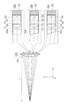
- the cross-sectional view which shows the composition of the pixel in the image pickup apparatus by 1st Embodiment.
- the plan view which shows the phase modulation part of a pixel in the image pickup apparatus of 1st Embodiment.
- the circuit diagram which shows the structure of the image pickup apparatus of 1st Embodiment.
- the plan view which shows the phase modulation part of a pixel in the image pickup apparatus by one modification of 1st Embodiment.
- the figure which shows the pixel arrangement of the image pickup apparatus by 2nd Embodiment The figure which shows the pixel arrangement of the image pickup apparatus by the 1st modification of 2nd Embodiment.
- FIG. 3 is a cross-sectional view showing an example of an optical member of an image pickup apparatus according to a first modification of the third embodiment.
- 12A and 12B are a cross-sectional view and a top view showing an example of an optical member of the image pickup apparatus according to the first modification of the third embodiment, respectively.
- the cross-sectional view which shows the manufacturing process of the image pickup apparatus according to 6th Embodiment The cross-sectional view which shows the manufacturing process of the image pickup apparatus according to 6th Embodiment.
- the cross-sectional view which shows the manufacturing process of the image pickup apparatus according to 6th Embodiment. The cross-sectional view which shows the manufacturing process of the image pickup apparatus according to 6th Embodiment.
- the cross-sectional view which shows the manufacturing process of the image pickup apparatus according to 6th Embodiment. which shows the manufacturing process of the image pickup apparatus according to 6th Embodiment.
- the cross-sectional view which shows the manufacturing process of the image pickup apparatus according to 6th Embodiment. The cross-sectional view which shows the manufacturing process of the image pickup apparatus according to 6th Embodiment.
- the image pickup apparatus of the first embodiment is an image sensor, and includes a pixel array having a plurality of pixels arranged in a matrix.
- FIG. 1 is a cross-sectional view of pixels arranged in one direction.
- a plurality of (for example, two) pixels 10 are arranged in the x direction, but a plurality of pixels (not shown) may be arranged in the y direction. That is, when m and n are positive integers, the pixels 10 may be arranged in a matrix of m rows ⁇ n columns in the pixel array.
- the z direction is a direction in which light from a subject (not shown) propagates.
- Each pixel 10 includes a light guide unit 12, a lens unit 14, a phase modulation unit 16, a light guide unit 18, a light shielding unit 20, and an image pickup element 30.
- the light guide unit 12 is arranged between a subject (not shown) and the image sensor 30, and propagates light from the subject to the lens unit 14.
- the light guide unit 12 is made of a material through which visible light is transmitted, and for example, a material having a refractive index of 1.55 for sodium D line (hereinafter, also simply referred to as D line) is used.
- the lens unit 14 is arranged between the light guide unit 12 and the image pickup element 30, and the light propagating through the light guide unit 12 propagates to the phase modulation unit 16.
- the lens unit 14 has, for example, a convex microlens, and the microlens has, for example, a refractive index of 1.9 for the D line.
- the phase modulation unit 16 is arranged between the lens unit 14 and the image pickup element 30, and has a phase difference (for example, a phase difference of a half wavelength of the wavelength ⁇ of visible light) of the light propagated from the lens unit 14. It separates into two lights and propagates to the light guide unit 18.
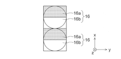
- the phase modulation unit 16 is divided into two portions 16a and 16b, for example, as shown in FIG. 2, the portion 16a is composed of, for example, a transparent material having a refractive index of 1.9 on the D line, and the portion 16b is formed.
- a transparent material having a refractive index of 1.55 for the D line is used, and a transparent material having a thickness (length in the z direction) of, for example, 0.7857 ⁇ m is used.
- the area of the portion 16a and the area of the portion 16b when viewed from the subject are substantially equal. That is, it means that the difference between the area of the portion 16a and the area of the portion 16b is within the manufacturing error range.
- FIG. FIG. 3 is a plan view of the phase modulation unit 16 as viewed from the subject.
- the circular solid line indicates the range of the light beam bundle that has passed through the lens portion 14.
- the light guide unit 18 is arranged between the phase modulation unit 16 and the image pickup element 30, and the light from the phase modulation unit 16 propagates to the light shielding unit 20.
- the light guide unit 18 is made of a material through which visible light is transmitted, and for example, a material having a refractive index of 1.55 for the D line is used.
- the light-shielding unit 20 is arranged between the light guide unit 18 and the image pickup element 30, and is provided on the surface of the light guide unit 18 facing the image pickup element 30 and the side surface of the light guide unit 18 (in the z direction).
- a portion 20b provided on a part of a parallel surface) is provided.
- the portion 20a is arranged at a position substantially separated from the lens portion 14 by a focal length of the microlens, and a pinhole 20c is provided in the center.
- the "substantial focal length” means a focal length within the range of manufacturing error of the microlens.
- the focal length of the microlens is preferably larger than 0.0003 mm and smaller than 3 mm.
- the diameter of the pinhole is preferably larger than 0.1 ⁇ m and smaller than 2 ⁇ m.
- the portion 20b is provided on the image pickup element 30 side of the side surface of the light guide unit 18 to prevent light from propagating from the side surface of the light guide unit 18 to other pixels. That is, the light shielding unit 20 propagates the light rays focused by the lens unit 14 via the phase modulation unit 16 and the light guide unit 18 to the image pickup device 30 through the pinhole 20c, and the light is adjacent to the pixels by the portion 20b. Propagate to and prevent crosstalk from occurring. That is, the portions 20a and 20b are made of a material that absorbs visible light.
- the image pickup device 30 includes a CCD (Charge Coupled Device) or CMOS image sensor element.
- the optical axis of the optical system including the light guide unit 12, the lens unit 14, the phase modulation unit 16, the light guide unit 18, and the light shielding unit 20 passes substantially the center of the image pickup element 30.
- a phase modulation unit 16 is provided, and the phase modulation unit 16 separates the light passing through the phase modulation unit 16 by the portion 16a and the portion 16b into two lights having a phase difference of half a wavelength.
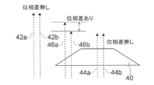
- the subject 40 has a trapezoidal cross section and is almost transparent, and when light is incident on the subject 40 from the opposite side of the image sensor, that is, the light is incident on the subject 40 from the lower side of the trapezoid and the upper side.
- Two light rays are paired and photoelectrically converted by an image sensor having the same pixel.
- One of the two light rays represents the light passing through the area center of the portion 16a of the phase modulation unit 16, and the other one represents the light passing through the area center of the portion 16b of the phase modulation unit 16.
- the phase difference is canceled in the image sensor, and the same image as when there is no phase difference is obtained. Since the light rays 46a and 46b shown in FIG. 3 pass through different positions on the hypotenuse of the subject 40, there is a phase difference. Therefore, the phase difference is different between the light ray passing through the area center of the portion 16a of the phase modulation unit 16 and the light ray passing through the area center of the part 16b of the phase modulation unit 16, and the phase difference is not canceled by the corresponding image pickup element. , An image with a phase difference is obtained. That is, it is possible to obtain an image having a differential interference contrast contrast, and it is possible to obtain a high-quality image.
- the portion 16a and the portion 16b are arranged separately in the x direction, so that the contrast of the image is generated along the x direction, and the obtained image is x. It looks like a three-dimensional image seen from the direction.
- the lens unit 14 made of a microlens is used to collect light in the pinhole 20c of the light shielding unit 20, it is possible to improve the efficiency of light utilization. Further, since a part of the side surface of the light guide portion 18 is covered by the portion 20b of the light shielding portion 20, cross stalk can be suppressed and the light utilization efficiency can be further improved.
- FIG. 4 shows the overall configuration of the image pickup apparatus of this embodiment.
- the image pickup apparatus 250 of this embodiment includes a pixel region 251, a pixel drive line 252, a vertical signal line 253, a vertical drive unit 254, a column processing unit 255, a horizontal drive unit 256, a system control unit 257, and the like. It includes a signal processing unit 258 and a memory unit 259. These are formed on a semiconductor substrate (chip) such as a silicon substrate (not shown).
- the pixel region 251 is formed on a sensor chip made of a first semiconductor substrate, and the pixel drive line 252, the vertical signal line 253, the vertical drive unit 254, the column processing unit 255, the horizontal drive unit 256, the system control unit 257, and the signal processing.
- a unit 258 and a memory unit 259 may be formed on a circuit chip made of a second semiconductor substrate, and these chips may be bonded together.
- the pixel region 251 is a pixel array in which the pixels 10 described in FIG. 1 are two-dimensionally arranged, and an optical signal is converted into an electric signal for imaging.
- a pixel drive line 252 is provided for every two rows of a pixel, and a vertical signal line 253 is provided for every two columns.
- the vertical drive unit 254 is configured by a shift register, an address decoder, or the like, and pixel signals corresponding to the charges stored in each image sensor in the pixel area 251 are read out in order from the top in the order of odd-numbered columns and even-numbered columns. As described above, the drive signal is supplied to the pixel drive line 252.
- the column processing unit 255 has a signal processing circuit for each of the two rows of pixels in the pixel area 251. Each signal processing circuit of the column processing unit 255 performs A / D conversion processing and correlated double sampling (CDS (Correlated Double Sampling)) for the pixel signal read from the corresponding pixel and supplied through the vertical signal line 253. ) Perform signal processing such as processing.
- the column processing unit 255 temporarily holds the pixel signal after signal processing.
- the horizontal drive unit 256 is composed of a shift register, an address decoder, etc., and sequentially selects the signal processing circuit of the column processing unit 255. As a result, the pixel signals signal-processed by each signal processing circuit of the column processing unit 255 are sequentially output to the signal processing unit 258.
- the system control unit 257 is composed of a timing generator or the like that generates various timing signals, and controls the vertical drive unit 254, the column processing unit 255, and the horizontal drive unit 256 based on the various timing signals generated by the timing generator. do.
- the signal processing unit 258 performs various signal processing on the pixel signal output from the column processing unit. At this time, the signal processing unit 258 stores the intermediate result of signal processing and the like in the memory unit 259 as necessary, and refers to the signal processing unit 258 at a necessary timing.
- the signal processing unit 258 outputs the pixel signal after signal processing.
- the memory unit 259 is composed of a DRAM (Dynamic Random Access Memory), a SRAM (Static Random Access Memory), or the like.
- the phase modulation unit 16 shown in FIG. 2 is used as the phase modulation unit 16A shown in FIG. 5, so that the subject is in the x-direction and the y-direction. You can see the difference in thickness.
- the phase modulation unit 16A has a portion 16a arranged in two regions located on one diagonal of the regions divided into two in the x direction and two in the y direction, and two regions located on the other diagonal. It has a configuration in which the portion 16b is arranged in. Also in FIG. 5, the areas of the portion 16a and the portion 16b are substantially the same.
- a specific wavelength for example, 940 nm
- a 1/2 wavelength phase plate having the specific wavelength is used as a portion 16a of the phase modulation unit 16A of each pixel. Can be done.
- this modification can also provide an image pickup device capable of obtaining a high-quality image with high light utilization efficiency.
- the image pickup apparatus according to the second embodiment will be described with reference to FIG.
- the first embodiment is an image pickup device that can obtain a monochromatic image
- the second embodiment is an image pickup device that can obtain a color image.
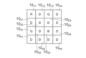
- FIG. 6 is a diagram showing a pixel arrangement of the image pickup apparatus of the second embodiment.
- Pixels 10 11 to 10 44 arranged in 4 rows and 4 columns are divided into 1st to 4th pixel groups with 4 pixels arranged in 2 rows and 2 columns as one unit.
- the first pixel group is composed of pixels 10 11 , 10, 12 , 10 21 , and 1022
- the second pixel group is composed of pixels 10 13 , 10 14 , 10 23 , and 10 24
- the third pixel group is composed of pixels. It is composed of 10 31 , 10 32 , 10 41 , and 10 42
- the fourth pixel group is composed of pixels 10 33 , 10 34 , 10 43 , and 10 44 .
- one pixel (for example, pixel 10 11 ) of the four pixels 10 11 , 10 12 12 , 10 21 and 10 22 of the first pixel group is a red pixel (hereinafter, also referred to as an R pixel).
- the other pixels are referred to as differential interference pixels (hereinafter, also referred to as D pixels).
- One pixel (for example, pixel 10 13 ) of the four pixels 10 13 , 10, 14 , 10 23 , and 10 24 of the second pixel group is a green pixel (hereinafter, also referred to as G pixel), and the other pixel is D. Let it be a pixel.
- One pixel (for example, pixel 10 31 ) of the four pixels 10 31 , 10 32 , 10 41 , and 10 42 in the third pixel group is a G pixel, and the other pixel is a D pixel.
- One pixel (for example, pixel 10 33 ) of the four pixels 10 33 , 10 34 , 10 43 , 10 44 of the fourth pixel group is a blue pixel (hereinafter, also referred to as B pixel), and the other pixel is a D pixel. And.
- the D pixel has the same configuration as the pixel 10 shown in FIG. 1, and the phase modulation unit 16 shown in FIG. 2 or the phase modulation unit 16A shown in FIG. 5 is used as the phase modulation unit.
- the D pixel of the first pixel group uses an R color half-wavelength phase plate as the phase modulation unit 16A
- the D pixel of the second pixel group is a G color half as the phase modulation unit 16A.
- a wavelength phase plate is used
- a G-color half-wave phase plate is used as the phase modulation unit 16A for the D pixel of the third pixel group
- a B-color half-wave phase of the D pixel of the fourth pixel group is used as the phase modulation unit 16A.
- a board is used.
- the R pixel replaces the phase modulation unit 16 of the pixel 10 shown in FIG. 1 with a red filter
- the G pixel replaces the phase modulation unit 16 of the pixel 10 shown in FIG. 1 with a green filter
- the B pixel is the pixel 10 shown in FIG. It has a configuration in which the phase modulation unit 16 is replaced with a B color filter.
- each pixel group is provided with one color pixel and the remaining three D pixels, and since these three D pixels are provided with a half-wavelength plate of the color of the color pixel, the above-mentioned color is emphasized in the image. Can be obtained.
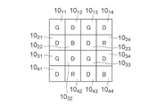
- FIG. 7 is a diagram showing a pixel arrangement of an image pickup apparatus according to a first modification of the second embodiment.
- the pixels 10 11 to 10 44 arranged in 4 rows and 4 columns are set as a pixel group in which 4 pixels arranged in 2 rows and 2 columns are used as one unit, and the first to 1st to 4 pixels are used. It is divided into a fourth pixel group.
- the first pixel group is composed of pixels 10 11 , 10, 12 , 10 21 , and 1022
- the second pixel group is composed of pixels 10 13 , 10 14 , 10 23 , and 10 24
- the third pixel group is composed of pixels. It is composed of 10 31 , 10 32 , 10 41 , and 10 42
- the fourth pixel group is composed of pixels 10 33 , 10 34 , 10 43 , and 10 44 .
- one pixel (for example, pixel 10 11 ) of the four pixels 10 11 1, 10 12 12 , 10 21 and 10 22 of the first pixel group is a G pixel.
- the other one pixel (for example, pixel 10 22 ) is a B pixel, and the remaining two pixels are D pixels.
- a G-color half-wavelength phase plate is used as the phase modulation unit 16A.
- One pixel (for example, pixel 10 13 ) of the four pixels 10 13 , 10, 14 , 10 23 , and 10 24 of the second pixel group is a G pixel
- the other pixel (for example, pixel 10 24 ) is an R pixel.
- the remaining two pixels are D pixels.
- a G-color half-wavelength phase plate is used as the phase modulation unit 16A.
- One pixel (for example, pixel 10 31 ) of the four pixels 10 31 , 10 32 , 10 41 , and 10 42 in the third pixel group is a G pixel, and the other pixel (for example, pixel 10 42 ) is an R pixel.
- the remaining two pixels be D pixels.
- a G-color half-wavelength phase plate is used as the phase modulation unit 16A.
- One pixel (for example, pixel 10 33 ) of the four pixels 10 33 , 10 34 , 10 43 , 10 44 of the fourth pixel group is a G pixel, and the other pixel (for example, pixel 10 44 ) is a B pixel.
- the remaining two pixels be D pixels.
- a B-color half-wavelength phase plate is used as the phase modulation unit 16A.
- FIG. 8 is a diagram showing a pixel arrangement of an image pickup apparatus according to a second modification of the second embodiment. Similar to the second embodiment, the pixels 10 11 to 10 44 arranged in 4 rows and 4 columns are set as a pixel group in which 4 pixels arranged in 2 rows and 2 columns are used as one unit, and the first to 1st to 4 pixels are used. It is divided into a fourth pixel group.
- the first pixel group is composed of pixels 10 11 , 10, 12 , 10 21 , and 1022
- the second pixel group is composed of pixels 10 13 , 10 14 , 10 23 , and 10 24
- the third pixel group is composed of pixels. It is composed of 10 31 , 10 32 , 10 41 , and 10 42
- the fourth pixel group is composed of pixels 10 33 , 10 34 , 10 43 , and 10 44 .
- one pixel (for example, pixel 10 11 ) of the four pixels 10 11 1, 10 12 12 , 10 21 and 10 22 of the first pixel group is an R pixel, and the other.
- One pixel (for example, pixel 10 12 ) is a G pixel
- another pixel (for example, pixel 10 21 ) is a B pixel
- the remaining one pixel (for example, pixel 10 22 ) is a D pixel.
- a G-color half-wavelength phase plate is used as the phase modulation unit 16A.
- One pixel (for example, pixel 10 13 ) of the four pixels 10 13 10, 10 14 10, 10 23 , 10 24 of the second pixel group is an R pixel, and the other pixel (for example, pixel 10 14 ) is a G pixel.
- another pixel for example, pixel 10 23
- B pixel another pixel
- D pixel the remaining one pixel
- a G-color half-wavelength phase plate is used as the phase modulation unit 16A.
- One pixel (for example, pixel 10 31 ) of the four pixels 10 31 , 10 32 , 10 41 , 10 42 of the third pixel group is an R pixel, and the other pixel (for example, pixel 10 32 ) is a G pixel.
- another pixel for example, pixel 10 41
- B pixel another pixel
- D pixel the remaining one pixel
- a G-color half-wavelength phase plate is used as the phase modulation unit 16A.
- One pixel (for example, pixel 10 33 ) of the four pixels 10 33 , 10 34 , 10 43 , 10 44 of the fourth pixel group is an R pixel, and the other pixel (for example, pixel 10 34 ) is a G pixel.
- another pixel for example, pixel 10 43
- B pixel another pixel
- D pixel the remaining one pixel
- a G-color half-wavelength phase plate is used as the phase modulation unit 16A.
- the first to fourth pixel groups each have the same array of pixels.
- the second modification of the second embodiment can also obtain a high-quality color image with high light utilization efficiency.
- FIG. 9 is a diagram showing a pixel arrangement of an image pickup apparatus according to a third modification of the second embodiment. Similar to the second embodiment, the pixels 10 11 to 10 44 arranged in 4 rows and 4 columns are set as a pixel group in which 4 pixels arranged in 2 rows and 2 columns are used as one unit, and the first to 1st to 4 pixels are used. It is divided into a fourth pixel group.
- the first pixel group is composed of pixels 10 11 , 10, 12 , 10 21 , and 1022
- the second pixel group is composed of pixels 10 13 , 10 14 , 10 23 , and 10 24
- the third pixel group is composed of pixels. It is composed of 10 31 , 10 32 , 10 41 , and 10 42
- the fourth pixel group is composed of pixels 10 33 , 10 34 , 10 43 , and 10 44 .
- one pixel for example, pixel 10 11 of the four pixels 10 11 1, 10 12 12 , 10 21 and 10 22 of the first pixel group is used as an R pixel, and the like.
- Two pixels for example, pixels 10 12 and 10 21 ) are G pixels, and the remaining one pixel (for example, pixels 10 22 ) is a D pixel.
- a G-color half-wavelength phase plate is used as the phase modulation unit 16A.
- One pixel (for example, pixel 10 13 ) of the four pixels 10 13 10, 10 14 10, 10 23 , 10 24 of the second pixel group is defined as a B pixel, and the other two pixels (for example, pixels 10 14 10 10 23 ) are used.
- a G-color half-wavelength phase plate is used as the phase modulation unit 16A.
- One pixel (for example, pixel 10 31 ) of the four pixels 10 31 , 10 32 , 10 41 , 10 42 of the third pixel group is defined as a B pixel, and the other two pixels (for example, pixels 10 32 , 10 41 ) are used.
- a G-color half-wavelength phase plate is used as the phase modulation unit 16A.
- One pixel (for example, pixel 10 33 ) of the four pixels 10 33 , 10 34 , 10 43 , 10 44 of the fourth pixel group is an R pixel, and the other two pixels (for example, pixels 10 34 , 10 43 ) are used.
- a G-color half-wavelength phase plate is used as the phase modulation unit 16A.
- FIG. 10 is a cross-sectional view of the image pickup apparatus of the third embodiment.
- the image pickup device 100 of the third embodiment is an optical member (for example, a convex lens) on a pixel array in which a plurality of pixels 10 are arranged in a matrix in the image pickup devices of the first embodiment and the second embodiment and modified examples thereof. ) 50 is further provided.
- an optical member for example, a convex lens
- the pixel 10a is a pixel corresponding to the central portion of the image obtained by the image pickup apparatus, and receives light rays passing through the central region 50a of the convex lens 50.
- the light rays that have passed through the region 50a propagate to the light guide unit 12 of the pixel 10a.
- the pixel 10c is a pixel corresponding to the vicinity of the end portion of the image obtained by the image pickup apparatus, and receives light rays passing through the region 50c near the end portion of the convex lens 50.
- the light rays that have passed through the region 50c propagate to the light guide unit 12 of the pixel 10c.
- the pixel 10b is a pixel corresponding to a region between the central portion and the vicinity of the end portion of the image obtained by the image pickup apparatus, and is a region 50b between the central region 50a of the convex lens 50 and the region 50c near the end portion. Receives light rays that pass through. The light rays that have passed through the region 50b propagate to the light guide unit 12 of the pixel 10b.
- the arrangement pitch of the image pickup device 30 is 5 ⁇ m
- the diagonal length d of the effective diameter of the image pickup device 100 is 3.3 mm
- the focal length f of the convex lens 50 is 10 mm.
- the diagonal length of the image is reduced from 3.3 mm to 1.65 mm, and the pixel pitch (resolution in a broad sense) is increased. Reduce from 5 ⁇ m to 2.5 ⁇ m. That is, it will be reduced to 1/2.
- the diagonal length of the image is reduced from 3.3 mm to 0.33 mm, and the resolution is reduced from 5 ⁇ m to 0.5 ⁇ m. That is, it will be reduced to 1/10.
- the diagonal length of the image is reduced from 3.3 mm to 0.033 mm, and the resolution is reduced from 5 ⁇ m to 0.05 ⁇ m. .. That is, it will be reduced to 1/100.
- the diagonal length of the image is reduced from 3.3 mm to 0.0066 mm and the resolution is reduced from 5 ⁇ m to 0.01 ⁇ m. .. That is, it will be reduced to 1/500.
- the image pickup apparatus of this embodiment has the same functions as a microscope and is a microscope that does not use an objective lens.
- the focal length of the convex lens 50 is preferably larger than 0.1 mm and smaller than 1000 mm.
- the image pickup apparatus 100 of the present embodiment is provided with the phase modulation unit 16 in each pixel, it is possible to observe a subject such as a cell that is almost transparent as in the image pickup apparatus of the first embodiment. Therefore, the obtained image has high image quality.
- the image pickup device of the second embodiment and its modified example is used as the image pickup device of the present embodiment, it is possible to obtain an image in which a nearly transparent subject is color-reproduced and color-enhanced.
- the convex lens 50 is usually made of a glass material.
- a plastic lens made of a plastic material may be used. In this case, it can be formed on a pixel array using a replica process.
- the third embodiment can provide an image pickup device capable of obtaining a high-quality image with high light utilization efficiency, similarly to the first embodiment.
- the image pickup apparatus according to the first modification of the third embodiment will be described with reference to FIG.
- the image pickup apparatus of the first modification has a configuration in which the optical member 50 is replaced with the Fresnel lens 52 shown in FIG. 11 in the image pickup apparatus 100 of the third embodiment.
- FIG. 11 is a cross-sectional view taken along a plane including the optical axis of the Fresnel lens 52.
- this first modification also makes it possible to observe a subject such as a cell that is almost transparent, and the obtained image has high image quality. Further, if the image pickup device of the second embodiment and the modification thereof is used as the image pickup device of the present modification, it is possible to obtain an image in which a nearly transparent subject is color-reproduced and color-enhanced.
- FIGS. 12A and 12B The image pickup apparatus according to the second modification of the third embodiment will be described with reference to FIGS. 12A and 12B.
- the image pickup apparatus of the second modification has a configuration in which the optical member 50 is replaced with the hologram 54 shown in FIGS. 12A and 12B in the image pickup apparatus 100 of the third embodiment.
- FIG. 12A is a cross-sectional view cut along a plane including the optical axis of the hologram 54
- FIG. 12B is a top view of the hologram 54.
- This hologram 54 utilizes a diffraction phenomenon, unlike a lens or the like that utilizes a refraction phenomenon.
- this first modification also makes it possible to observe a subject such as a cell that is almost transparent, and the obtained image has high image quality. Further, if the image pickup device of the second embodiment and the modification thereof is used as the image pickup device of the present modification, it is possible to obtain an image in which a nearly transparent subject is color-reproduced and color-enhanced.
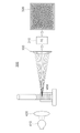
- the electronic device 300 is a system for displaying a microscope for observing a subject such as cells that are almost transparent and an image thereof, and includes an image pickup device 100, a processing unit 310, and a display unit 320.
- the image pickup device 100 is the image pickup device of the third embodiment.
- a PC Personal Computer
- the processing unit 310 is used as the processing unit 310 to process the signal supplied from the signal processing unit 258 shown in FIG. 4 to obtain image data.
- the display device 320 displays an image using the image data supplied from the processing unit 310.
- the light beam emitted from the light source 410 is applied to the well 450 containing the sample (for example, cells) through the lens 420.
- the light beam transmitted through the well 450 is imaged by the image pickup device 100, the image pickup result is processed by the processing unit 310, and the processing result is displayed by the display device 320.
- the image pickup device 100 the image pickup device of the first modification or the second modification of the third embodiment may be used.
- the electronic device of the fourth embodiment can observe a subject such as a cell that is almost transparent, and the obtained image has high image quality.
- the image pickup device 100 of the present embodiment is used as the image pickup device of the second embodiment and its modified example, it is possible to obtain an image in which a nearly transparent subject is color-reproduced and color-enhanced.
- the image pickup apparatus according to the fifth embodiment is shown in FIG.
- the image pickup device 100A of the fifth embodiment includes a configuration in which the phase modulation section 16 is deleted from each pixel and the light-shielding section 20 is replaced with the light-shielding section 20A in the image pickup device 100 of the third embodiment shown in FIG. ing.
- the pixels 10Aa, 10Ab, and 10Ac shown in FIG. 14 correspond to the pixels 10a, 10b, and 10c shown in FIG. 10, respectively.
- the light-shielding portion 20A has a configuration in which the pinhole 20c is removed from the light-shielding portion 20 shown in FIG. That is, in the light-shielding portion 20A, the pinhole 20c provided on a part of the side surface of the light guide portion 18 is deleted.
- the lens portion 14 made of a microlens is used to collect light in the pinhole of the light shielding portion 20A, so that the efficiency of light utilization is improved. be able to.
- FIG. 15 is a schematic cross-sectional configuration diagram of an image pickup apparatus manufactured by the manufacturing method of the present embodiment.
- a first semiconductor chip portion 500 including a pixel array (hereinafter, also referred to as a pixel region) and a control circuit, and a second semiconductor chip portion 700 on which a logic circuit is mounted are electrically connected up and down. It is laminated in.
- an image sensor in a semi-finished state is provided in a region to be a chip portion of the first semiconductor wafer (hereinafter, also referred to as a first semiconductor substrate) 510. It forms a control region 530 with 520. That is, for example, a photodiode (PD) to be a photoelectric conversion part of each pixel is formed in a region to be a chip portion of a first semiconductor substrate 510 made of a silicon substrate, and a source / source of each pixel transistor is formed in the semiconductor well region 512.
- the drain region 514 is formed.
- the semiconductor well region 512 is formed by introducing a first conductive type, for example, p-type impurity, and the source / drain region 514 is formed by introducing a second conductive type, for example, n-type impurity.
- the photodiode (PD) and the source / drain region 514 of each pixel transistor are formed by ion implantation from the substrate surface.
- the photodiode (PD) has an n-type semiconductor region 516 and a p-type semiconductor region 517 on the substrate surface side.
- a gate electrode 518 is formed on the surface of the substrate constituting the pixel via a gate insulating film, and pixel transistors Tr1 and Tr2 are formed by a source / drain region 514 paired with the gate electrode 518.
- a plurality of pixel transistors are represented by two pixel transistors Tr1 and Tr2.
- the pixel transistor Tr1 adjacent to the photodiode (PD) corresponds to a transfer transistor, and its source / drain region corresponds to a floating diffusion (FD).
- Each unit pixel is separated by the element separation region 522.
- a MOS transistor constituting the control region 530 is formed on the first semiconductor substrate 510.
- FIG. 16 shows MOS transistors constituting the control region 530, represented by MOS transistors Tr3 and Tr4.
- Each MOS transistor Tr3 and Tr4 includes an n-type source / drain region 514 and a gate electrode 518 formed via a gate insulating film. The MOS transistors Tr3 and Tr4 are separated by the element separation region 525.
- the first layer of the interlayer insulating film 540 is formed on the surface of the first semiconductor substrate 510, and then a contact hole is formed in the interlayer insulating film 540 to form a connecting conductor 542 to be connected to a required transistor.
- a first insulating thin film for example, a silicon oxide film is formed on the entire surface including the upper surface of the transistor, and as a second insulating thin film (not shown) as an etching stopper.
- it is formed of a silicon nitride film and laminated.
- a second interlayer insulating film 540 is formed on the second insulating thin film. After that, contact holes having different depths are selectively formed in the second interlayer insulating film 540 up to the second insulating thin film (not shown) as an etching stopper.
- the first insulating thin film (not shown) and the second insulating thin film (not shown) having the same film thickness are selectively etched in each part so as to be connected to each contact hole to form a contact hole.
- the connecting conductor 542 is embedded in each contact hole.
- each copper wiring 546 is formed. Normally, each copper wiring 546 is covered with a barrier metal layer (not shown) in order to prevent Cu diffusion.
- the first multilayer wiring layer 550 is formed by alternately forming the interlayer insulating film 540 and the copper wiring 546 formed via the barrier metal layer.
- the first multilayer wiring layer 550 is formed of copper wiring 546, but metal wiring made of other metal materials is also possible.
- the first semiconductor chip portion 500 having the first multilayer wiring layer 550 on the upper portion and having the pixel region 520 and the control region 530 in the semi-finished state is formed.
- a logic circuit 710 including a signal processing circuit for processing a signal in a semi-finished product state is formed in a region to be a chip portion of a second semiconductor substrate (semiconductor wafer) 720 made of silicon, for example. do. That is, a plurality of MOS transistors constituting the logic circuit 710 are formed in the p-type semiconductor well region 722 on the surface side of the second semiconductor substrate 720 so as to be separated by the element separation region 725.
- a plurality of MOS transistors are represented by MOS transistors Tr11, Tr12, and Tr13.
- Each of the MOS transistors Tr11, Tr12, and Tr13 has a pair of n-type source / drain regions 730 and a gate electrode 732 formed via a gate insulating film (not shown).
- the logic circuit 710 can be configured with a CMOS transistor.
- the first layer of the interlayer insulating film 740 is formed on the surface of the second semiconductor substrate 720, and then a contact hole is formed in the interlayer insulating film 740.
- a connecting conductor 742 is formed to connect to a required transistor so as to embed this contact hole.
- a silicon oxide film as a first insulating thin film (not shown) and a second insulating thin film as an etching stopper are formed on the entire surface including the upper surface of the transistor, as in the case described above.
- a silicon nitride film is laminated.
- a second interlayer insulating film 740 is formed on the second insulating thin film. Then, contact holes having different depths are selectively formed in the second interlayer insulating film 640 up to the second insulating thin film (not shown) which serves as an etching stopper.
- the first insulating thin film (not shown) and the second insulating thin film (not shown) having the same film thickness are selectively etched in each part so as to be connected to each contact hole to form a contact hole.
- the second multilayer wiring layer 750 is formed by repeating the formation of the interlayer insulating film 740 and the formation of the metal wiring of a plurality of layers.
- the four layers of copper wiring 752 are formed by using the same process as the step of forming the first multilayer wiring layer 550 formed on the first semiconductor substrate 510, and the second multilayer wiring layer 750 is formed. ..
- a warp correction film 760 for reducing warpage when the first semiconductor substrate 610 and the second semiconductor substrate 720 are bonded is formed on the upper part of the second multilayer wiring layer 750.
- a second semiconductor substrate 720 having a second multilayer wiring layer 750 on the upper portion and having a logic circuit in a semi-finished state is formed on the upper part of the second multilayer wiring layer 750.
- the first semiconductor substrate 510 and the second semiconductor substrate 720 are bonded so that the first multilayer wiring layer 550 and the second multilayer wiring layer 750 face each other.
- the bonding is performed with, for example, an adhesive. In addition, they may be bonded by plasma bonding.
- the first multilayer wiring layer 550 having the multilayer wiring layer on the upper portion and the second semiconductor substrate 720 are laminated and laminated to form a laminated body 800 composed of two different types of substrates.
- the first semiconductor substrate 510 is thinned by grinding and polishing from the back surface side of the first semiconductor substrate 510. This thinning is performed so that the back surface of the photodiode (PD), that is, the n-type semiconductor region 516 is exposed. After thinning, a p-type semiconductor layer (not shown) for suppressing dark current is formed on the back surface of the photodiode (PD).
- the thickness of the first semiconductor substrate 510 is, for example, about 600 ⁇ m, but the thickness of the first semiconductor substrate 510 is reduced to, for example, about 3 to 5 ⁇ m.
- the back surface of the first semiconductor substrate 510 is a light incident surface when configured as a back-illuminated image pickup device.
- an antireflection coating 810 is applied to the back surface of the first semiconductor substrate 510.
- a tungsten film 820 is formed on the photodiode (PD) with a thickness of, for example, 350 nm.
- the surface is polished by a CMP (Chemical Mechanical Polishing) method, and pinhole 822 is formed by etching.
- a light-shielding film groove portion 830 which requires light-shielding, is formed.
- the light-shielding film groove portion 830 is formed by forming an opening by etching from the upper surface of the insulating film 826 formed on the back surface side of the first semiconductor substrate 510. This opening is formed, for example, at a depth that does not reach the first semiconductor substrate 510.
- a tungsten (W) film is formed and the surface is polished by the CMP method.
- the tungsten in the light-shielding film groove portion 830 remains, and the light-shielding film 832 is formed in the light-shielding region.
- phase plate 840 that occupies an area of about 1/2 of the effective diameter of the sensor is formed.
- the phase plate 840 forms, for example, a thin film of silicon nitride on the flattening film 836, and a photoresist is formed on the silicon nitride film.
- a mask (not shown) having a hole in the shape of a half-wavelength phase plate is formed.
- exposure and development are performed, and then the photoresist in the area not covered by the mask is removed. Then, using the above mask. It can be formed by etching the silicon nitride film, then peeling off the photoresist and performing cleaning. The mask is removed when the photoresist is peeled off.
- red (R), green (G), and blue (B) on-chip color filters 860 are formed on the flattening film 836 corresponding to each pixel.
- the on-chip color filter 860 can be formed on the top of the photodiode (PD) constituting the desired pixel array by forming an organic film containing a pigment or dye of a desired color and patterning the organic film. .. Then, the on-chip lens material 870 is formed in the pixel array region including the upper part of the on-chip color filter 860.
- a resist film for an on-chip lens is formed in a region corresponding to each pixel on the upper part of the on-chip lens material 870, and an etching process is performed to form an on-chip lens 872. ..
- the convex lens 50 of the third embodiment shown in FIG. 10 of the present disclosure is formed with an air gap.
- the adhesive layer 880 may be formed to form the convex lens 50.
- the Fresnel lens 52 shown in FIG. 11 may be formed.
- the hologram 54 shown in FIGS. 12A and 12B may be formed.
- the convex lens 50 can be bonded by using a plastic mold lens or a glass mold lens.
- a wafer level lens manufactured by a replica process may be formed by step and repeat.
- the hologram 54 may be formed after the adhesive layer 880 is formed, the cover glass is adhered, and the thickness is reduced to, for example, 50 ⁇ m.
- the hologram manufactured by this manufacturing method has a four-step step shape.
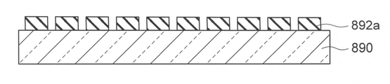
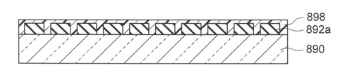
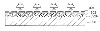
- the adhesive layer 880 shown in FIG. 23 is formed on the upper layer of the light incident surface (back surface), and then the cover glass 890 is adhered. Subsequently, for example, the cover glass 890 is thinned to 50 ⁇ m, and a silicon oxide film 892 having a thickness of 0.4 ⁇ m is formed on the cover glass 890. A photoresist film 894 is formed on the silicon oxide film 892.
- a mask having a hole in the shape of the first stage of the hologram is formed on the photoresist film 894, and the photoresist film 894 is exposed (FIG. 25).
- the exposed photoresist and mask 896 are removed.
- a mask 894a made of a photoresist is formed (FIG. 26).
- the silicon oxide film 892 is etched using this mask 894a.
- the silicon oxide film becomes a patterned silicon oxide film 892a (FIG. 27).
- the mask 894a made of the photoresist is removed, and then cleaning is performed. This completes the first stage of the step hologram made of the silicon oxide film 892a (FIG. 28).
- a photoresist film 898 is formed on the silicon oxide film 892a and between the adjacent silicon oxide films 892a (FIG. 29). Subsequently, a mask 900 having a hole in the shape of a second stage of the hologram is formed on the photoresist film 898. The photoresist film 898 is exposed using this mask 900 (FIG. 30).
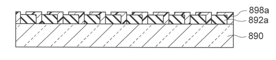
- the exposed photoresist film 898 is developed, the exposed photoresist film 898 is removed, and the mask 900 is also removed. As a result, a mask 898a made of a photoresist is formed (FIG. 31).
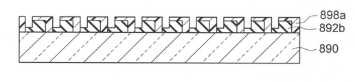
- the silicon oxide film 892a is etched using the mask 898a (FIG. 32). Subsequently, the mask 898a made of a photoresist is peeled off and washed. This completes the silicon oxide film 892b having the first and second stages of the stepped hologram (FIG. 33).
- a photoresist film 902 is formed on the silicon oxide film 892b and between the adjacent silicon oxide films 892b (FIG. 34).
- a mask 904 provided with a hole in the shape of the third stage of the hologram is formed on the photoresist film 902. Subsequently, the photoresist film 902 is exposed using this mask 904 (FIG. 35).
- the photoresist film 902 is developed, the exposed photoresist is removed, and a mask 902a made of the photoresist is formed. At this time, the mask 904 is also removed (FIG. 36).
- the silicon oxide film 892b is etched using the mask 902a.
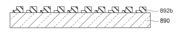
- the third stage of the stepped hologram is completed, and the silicon oxide film 892c that shakes the first stage, the second cross section, and the third stage is formed (FIG. 37).
- the mask 902a made of photoresist is removed and washed. This completes the hologram made of the silicon oxide film 892c, which also has the fourth stage of the stepped hologram (FIG. 38).
- At least one pixel is provided, and the pixel is It passes through a lens unit that collects incident light, a phase modulation unit that modulates the phase of a part of the light that has passed through the lens unit, and light whose phase is modulated by the phase modulation unit and light whose phase is not modulated.
- An image pickup device including a light-shielding portion having a pinhole for causing the light to be formed, and an image pickup element for capturing light that has passed through the pinhole.
- the phase modulation unit has a first portion and a second portion, and a phase difference of 1 ⁇ 2 of the wavelength between the light passing through the first portion and the light passing through the second portion.
- the imaging apparatus which is configured to generate the above.
- the image pickup apparatus according to any one of (1) to (3), which is arranged closer to the subject than the lens portion and further includes a first light guide portion that guides the subject light to the lens portion.
- the second light guide section (1) to (4) which is arranged between the phase modulation section and the light-shielding section and guides the light passing through the phase modulation section to the light-shielding section.
- the light-shielding portion includes a first member having the pinhole and arranged in a direction intersecting the propagation direction of light passing through the phase modulation portion, and the phase modulation portion from the peripheral portion of the first member.
- the image pickup apparatus according to (5) which has a second member extending in the direction of the above and arranged on the side of the second light guide portion.
- a plurality of pixels arranged in a matrix are provided, and each pixel has a lens unit that collects incident light and a light-shielding unit having a pinhole that allows at least a part of the light that has passed through the lens unit to pass through.
- An image pickup element that captures light that has passed through the pinhole, and at least one of the plurality of pixels has a phase modulation unit that modulates the phase of a part of the light that has passed through the lens unit.
- the light-shielding portion of the pixel having the phase-modulating section is an image pickup device having the pinhole for passing light whose phase is modulated by the phase-modulating section and light whose phase is not modulated by the phase-modulating section.
- the phase modulation unit has a first portion and a second portion, and a phase difference of 1 ⁇ 2 of the wavelength between the light passing through the first portion and the light passing through the second portion.
- the image pickup apparatus according to (7) or (8), wherein the phase modulation unit has substantially the same area as the first portion and the second portion.
- the image pickup apparatus according to any one of (7) to (9), further comprising a second light guide portion for guiding light to the light shielding portion.
- the light-shielding portion includes a first member having the pinhole and arranged in a direction intersecting the propagation direction of light passing through the phase modulation portion, and the phase modulation portion from the peripheral portion of the first member.
- the image pickup apparatus which extends in the direction of the above and is arranged on the side portion of the second light guide portion.
- the plurality of pixels are arranged in units of pixel groups having first to fourth pixels arranged in two adjacent rows and two columns, and the first to third pixels have the phase modulation unit.
- the image pickup apparatus according to any one of (7) to (11), wherein the fourth pixel does not have the phase modulation section and has a color filter arranged between the image pickup element and the lens section.
- the plurality of pixels are arranged in units of pixel groups having first to fourth pixels arranged in two adjacent rows and two columns, and the first to second pixels have the phase modulation unit.
- the third to fourth pixels are described in any one of (7) to (11), wherein the third to fourth pixels do not have the phase modulation unit and have different color filters arranged between the image pickup element and the lens unit.
- Imaging device (14)
- the plurality of pixels are arranged in units of pixel groups having first to fourth pixels arranged in two adjacent rows and two columns, and the first pixel has the phase modulation unit, and the first pixel is the first. 2.
- the plurality of pixels are arranged in units of pixel groups having first to fourth pixels arranged in two adjacent rows and two columns, and the first pixel has the phase modulation unit, and the first pixel is the first.
- the second to third pixels do not have the phase modulation unit, and have a first color filter of the same color arranged between the image pickup element and the lens unit, and the fourth pixel has the phase modulation unit.
- the image pickup apparatus according to any one of (7) to (11), which does not have a second color filter and has a second color filter having a color different from that of the first color filter arranged between the image pickup element and the lens portion. ..
- the image pickup apparatus according to (7) to (15), further comprising an optical member arranged between the plurality of pixels and a subject and condensing light from the subject onto the plurality of pixels.
- the optical member is a convex lens.
- the optical member is a Fresnel lens.
- the image pickup apparatus according to (16), wherein the optical member is a hologram.
- the image pickup apparatus includes an image pickup apparatus and a signal processing unit that performs signal processing based on a pixel signal imaged by the image pickup apparatus, and the image pickup apparatus includes a plurality of pixels arranged in a matrix, and each pixel is provided.
- a lens unit that collects incident light
- a light-shielding unit having a pinhole that allows at least a part of the light that has passed through the lens group
- an image pickup element that captures the light that has passed through the pinhole.
- At least one of the plurality of pixels has a phase modulation section that modulates the phase of a part of light that has passed through the lens section, and the light-shielding section of the pixel having the phase modulation section is the light-shielding section.
- An electronic device having the pinhole for passing light whose phase is modulated and light whose phase is not modulated by a phase modulator.
Landscapes
- Physics & Mathematics (AREA)
- General Physics & Mathematics (AREA)
- Optics & Photonics (AREA)
- Engineering & Computer Science (AREA)
- Multimedia (AREA)
- Signal Processing (AREA)
- Transforming Light Signals Into Electric Signals (AREA)
- Solid State Image Pick-Up Elements (AREA)
- Stereoscopic And Panoramic Photography (AREA)
Abstract
[課題]光の利用効率が高く高画質の画像を得ることが可能な撮像装置およびこの撮像装置を用いた電子機器を提供する。 [解決手段]本開示の撮像装置は、少なくとも1つの画素を備え、前記画素は、入射光を集光するレンズ部と、前記レンズ部を通過した一部の光の位相を変調する位相変調部と、前記位相変調部で位相が変調された光と位相が変調されない光とを通過させるピンホールを有する遮光部と、前記ピンホールを通過した光を撮像する撮像素子と、 を備えている。
Description
本開示の実施形態は、撮像装置および電子機器に関する。
複数の画素を有する撮像装置(センサ)と、撮像装置の単位画素と同じサイズレベルのマイクロレンズを複数個有するマイクロレンズアレイと、を備えた画像認識システムが知られている。
この画像認識システムにおいては、各マイクロンズと対応するセンサとの間に1つまたは2つのピンホールが設けられている。そして、マイクロレンズアレイのうち中央に位置しているマイクロレンズの光軸に対して、周縁側により近いマイクロレンズほど、光軸の傾斜角度を大きくしてくる。これにより、広い画角で被写体像を認識することができる。
しかし、この画像認識システムにおいては、ピンホールを用いて入射光の範囲を制限しているため、光の利用効率が低い。また、マイクロレンズアレイの周縁に近づくに従って、円形のピンホールを通過した光束の断面が歪んだ楕円になり、ピンホールで所望の画角の光線を選択してセンサアレイに到達させることができず、良質の画質を得ることが難しい。
本開示では、光の利用効率が高く高画質の画像を得ることが可能な撮像装置およびこの撮像装置を用いた電子機器を提供する。
本開示の第1態様による撮像装置は、少なくとも1つの画素を備え、前記画素は、
入射光を集光するレンズ部と、前記レンズ部を通過した一部の光の位相を変調する位相変調部と、前記位相変調部で位相が変調された光と位相が変調されない光とを通過させるピンホールを有する遮光部と、前記ピンホールを通過した光を撮像する撮像素子と、を備えている。
入射光を集光するレンズ部と、前記レンズ部を通過した一部の光の位相を変調する位相変調部と、前記位相変調部で位相が変調された光と位相が変調されない光とを通過させるピンホールを有する遮光部と、前記ピンホールを通過した光を撮像する撮像素子と、を備えている。
第1態様による撮像装置において、前記位相変調部は、第1部分と、第2部分とを有し、前記第1部分を通過した光と前記第2部分を通過した光とで、波長の1/2の位相差を生じるように構成されていてもよい。
第1態様による撮像装置において、前記位相変調部は、前記第1部分と前記第2部分は実質的に同じ面積を有していてもよい。
第1態様による撮像装置において、前記レンズ部よりも被写体側に配置され、被写体光を前記レンズ部に導光する第1導光部を更に備えていてもよい。
第1態様による撮像装置において、前記位相変調部と前記遮光部との間に配置され前記位相変調部を通過した光を前記遮光部に導光する第2導光部を更に備えていてもよい。
第1態様による撮像装置において、前記遮光部は、前記ピンホールを有し前記位相変調部を通過した光の伝搬方向に交差する方向に配置された第1部材と、前記第1部材の周縁部から前記位相変調部の方向に延び前記第2導光部の側部に配置される第2部材と、を有していてもよい。
第2態様による撮像装置は、マトリクス状に配列された複数の画素を備え、各画素は、入射光を集光するレンズ部と、前記レンズ部を通過した光の少なくとも一部を通過させるピンホールを有する遮光部と、前記ピンホールを通過した光を撮像する撮像素子と、を備え、前記複数の画素のうち少なくとも1つの画素は、前記レンズ部を通過した一部の光の位相を変調する位相変調部を有し、前記位相変調部を有する前記画素の前記遮光部は、前記位相変調部で位相が変調された光と変調されない光とを通過させる前記ピンホールを有する。
第2態様による撮像装置において、前記位相変調部は、第1部分と、第2部分とを有し、前記第1部分を通過した光と前記第2部分を通過した光とで、波長の1/2の位相差を生じるように構成されていてもよい。
第2態様による撮像装置において、前記位相変調部は、前記第1部分と前記第2部分は実質的に同じ面積を有していてもよい。
第2態様による撮像装置において、前記レンズ部よりも被写体側に配置され、被写体光を前記レンズ部に導光する第1導光部と、前記レンズ部と前記遮光部との間に配置され前記レンズ部からの光線を前記遮光部に導光する第2導光部と、を更に備えていてもよい。
第2態様による撮像装置において、前記遮光部は、前記ピンホールを有し前記位相変調部を通過した光の伝搬方向に交差する方向に配置された第1部材と、前記第1部材の周縁部から前記位相変調部の方向に延び前記第2導光部の側部に配置されていてもよい。
第2態様による撮像装置において、前記複数の画素は、隣接する2行2列に配置された第1乃至第4画素を有する画素群を単位として配置され、前記第1乃至第3画素は前記位相変調部を有し、前記第4画素は前記位相変調部を有せず、かつ前記撮像素子と前記レンズ部との間に配置される色フィルタを有していてもよい。
第2態様による撮像装置において、前記複数の画素は、隣接する2行2列に配置された第1乃至第4画素を有する画素群を単位として配置され、前記第1乃至第2画素は前記位相変調部を有し、前記第3乃至第4画素は前記位相変調部を有せず、かつ前記撮像素子と前記レンズ部との間に配置される異なる色フィルタを有していてもよい。
第2態様による撮像装置において、前記複数の画素は、隣接する2行2列に配置された第1乃至第4画素を有する画素群を単位として配置され、前記第1画素は前記位相変調部を有し、前記第2乃至第4画素は前記位相変調部を有せず、かつ前記撮像素子と前記レンズ部との間に配置される互いに異なる色フィルタを有していてもよい。
第2態様による撮像装置において、前記複数の画素は、隣接する2行2列に配置された第1乃至第4画素を有する画素群を単位として配置され、前記第1画素は前記位相変調部を有し、前記第2乃至第3画素は前記位相変調部を有せず、かつ前記撮像素子と前記レンズ部との間に配置される同色の第1色フィルタを有し、前記第4画素は、前記位相変調部を有せず、かつ前記撮像素子と前記レンズ部との間に配置される前記第1色フィルタと異なる色の第2色フィルタを有していてもよい。
第2態様による撮像装置において、前記複数の画素と被写体との間に配置され、前記被写体からの光を前記複数の画素に集光する光学部材を更に備えていてもよい。
第2態様による撮像装置において。前記光学部材は凸レンズであってもよい。
第2態様による撮像装置において、前記光学部材はフレネルレンズであってもよい。
第2態様による撮像装置において、前記光学部材はホログラムであってもよい。
第3態様による電子機器は、撮像装置と、前記撮像装置で撮像された画素信号に基づいて信号処理を行う信号処理部と、を備え、前記撮像装置は、マトリクス状に配列された複数の画素を備え、各画素は、入射光を集光するレンズ部と、前記レンズ群を通過した光の少なくとも一部を通過させるピンホールを有する遮光部と、前記ピンホールを通過した光を撮像する撮像素子と、を備え、前記複数の画素のうち少なくとも1つの画素は、前記レンズ部を通過した一部の光の位相を変調する位相変調部を有し、
前記位相変調部を有する前記画素の前記遮光部は、前記位相変調部で位相が変調された光と変調されない光とを通過させる前記ピンホールを有する。
前記位相変調部を有する前記画素の前記遮光部は、前記位相変調部で位相が変調された光と変調されない光とを通過させる前記ピンホールを有する。
本開示の実施形態について図面を参照して説明する。以下の実施形態では、撮像装置および電子機器の構成部分を主に説明するが、撮像装置および電子機器には、図示又は説明されていない構成部分や機能が存在しうる。以下の説明は、図示又は説明されていない構成部分や機能を除外するものではない。
また、以下の説明で参照される図面は、本開示の実施形態の説明と、その理解を促すための図面であり、分かり易くするために、図中に示される形状、寸法、比などは実際と異なる場合がある。
(第1実施形態)
第1実施形態による撮像装置について図1乃至図5を参照して説明する。第1実施形態の撮像装置はイメージセンサであって、マトリクス状に配列された複数の画素を有する画素アレイを備えている。図1は、一方向に配列された画素の断面図である。図1では、複数(例えば2個)の画素10がx方向に配列されているが、y方向に図示しない複数の画素が配列されていてもよい。すなわち、m、nを正の整数とした場合に、画素アレイは、画素10がm行×n列のマトリクス状に配列されていてもよい。なお、z方向は図示しない被写体からの光が伝播する方向である。
第1実施形態による撮像装置について図1乃至図5を参照して説明する。第1実施形態の撮像装置はイメージセンサであって、マトリクス状に配列された複数の画素を有する画素アレイを備えている。図1は、一方向に配列された画素の断面図である。図1では、複数(例えば2個)の画素10がx方向に配列されているが、y方向に図示しない複数の画素が配列されていてもよい。すなわち、m、nを正の整数とした場合に、画素アレイは、画素10がm行×n列のマトリクス状に配列されていてもよい。なお、z方向は図示しない被写体からの光が伝播する方向である。
各画素10は、導光部12と、レンズ部14と、位相変調部16と、導光部18と、遮光部20と、撮像素子30と、を備えている。
導光部12は、図示しない被写体と撮像素子30との間に配置され、被写体からの光をレンズ部14に伝播する。この導光部12は可視光が透過する材料で構成され、例えばナトリウムのD線(以下、単にD線とも云う)の屈折率が1.55の材料が用いられる。
レンズ部14は導光部12と撮像素子30との間に配置され、導光部12を伝播してきた光を位相変調部16に伝播する。このレンズ部14として、例えば凸形状のマイクロレンズを有し、このマイクロレンズは、例えばD線の屈折率が1.9となっている。
位相変調部16は、レンズ部14と撮像素子30との間に配置され、レンズ部14から伝播されてきた光を、位相差(例えば可視光の波長λの半波長の位相差)を有する2つの光に分離し、導光部18に伝播する。この位相変調部16は、例えば図2に示すように、2つの部分16a、16bに分けられ、部分16aは例えばD線の屈折率が1.9の透明体の材料で構成し、部分16bは例えばD線の屈折率が1.55の透明材料で構成し、それぞれの厚さ(z方向の長さ)が例えば0.7857μmの透明材料が用いられる。図2において、被写体から見たときの部分16aの面積と部分16bの面積は実質的に等しい。すなわち、部分16aの面積と部分16bの面積との差は製造誤差範囲内にあること意味する。
この構成により、部分16aと部分16bを透過した光に1/2波長の位相差が生じる。なお、図2は。位相変調部16を被写体からみた平面図である。図2において、円形の実線は、レンズ部14を通過した光線束の範囲を示している。
導光部18は位相変調部16と撮像素子30との間に配置され、位相変調部16からの光を遮光部20に伝播する。この導光部18は導光部12と同様に、可視光が透過する材料で構成され、例えばD線の屈折率が1.55の材料が用いられる。
遮光部20は、導光部18と撮像素子30との間に配置され、撮像素子30に対向する導光部18の面に設けられた部分20aと、導光部18の側面(z方向に平行な面)の一部に設けられた部分20bとを、備えている。部分20aは、レンズ部14からマイクロレンズの実質的焦点距離離れた位置に配置され、中央にピンホール20cが設けられている。ここで、「実質的焦点距離」とは、マイクロレンズの製造誤差の範囲内の焦点距離であることを意味する。なお、マイクロレンズの焦点距離は、0.0003mmより大きく3mmよりも小さいことが好ましい。また、ピンホールの直径は0.1μmより大きく2μmよりも小さいことが好ましい。
部分20bは導光部18の側面の撮像素子30側に設けられ、導光部18の側面から光が他の画素に伝播するのを防止する。すなわち、遮光部20は、レンズ部14によって位相変調部16および導光部18を介して集光された光線を、ピンホール20cを通して撮像素子30に伝播するとともに、部分20bによって光が隣接する画素に伝播しクロストークが生じることを防止する。すなわち、部分20a、20bは可視光を吸収する材料で構成される。
撮像素子30は、CCD(Charge Coupled Device)またはCMOSイメージセンサ素子を備えている。
各画素10において、導光部12,レンズ部14、位相変調部16、導光部18、および遮光部20からなる光学系の光軸は、撮像素子30のほぼ中心を通る。
本実施形態においては、位相変調部16が設けられ、この位相変調部16は、部分16aと部分16bによって位相変調部16を通過する光を半波長の位相差を有する2つの光に分離する。これにより、被写体が細胞などの透明に近いものをより見え易くすることが可能になる。このことについて図3を参照して以下に説明する。例えば。図3に示すように被写体40として、断面が台形形状で透明に近いものとし、撮像素子と反対側から被写体40に光が入射する場合、すなわち台形の下辺側から光が被写体40に入射し上辺側から画素に出射する場合を考える。2本の光線がペアとなり、同一の画素の撮像素子で光電変換されると仮定する。2本の光線のうち1本は位相変調部16の部分16aの面積中心を通過する光を表し、他の1本は位相変調部16の部分16bの面積中心を通過する光を表す。
図3に示す光線42a、42bは被写体40を通過しないので、2本の光線42a、42bに位相差は生じない。このため、位相変調部16の部分16aを通過した光線42aと部分16bを通過した光線42bは対応する撮像素子において位相差が打ち消され、位相差が無い場合と同じ画像が得られる。図3に示す光線44a、44bは被写体40の台形形状の下辺および上辺を透過しているので、透過後の光線44a、44bに位相差が生じず、光線42a、42bの場合と同様に、対応する撮像素子において位相差が打ち消され、位相差が無い場合と同じ画像が得られる。図3に示す光線46a、46bは被写体40の斜辺の異なる位置を通過しているため、位相差がある。このため、位相変調部16の部分16aの面積中心を通過した光線と、位相変調部16の部分16bの面積中心を通過した光線とで位相差が異なり、対応する撮像素子で位相差が打ち消されず、位相差がある画像が得られる。すなわち、微分干渉コントラストを有する画像を得ることが可能となり、高画質の画像を得ることができる。
なお、第1実施形態では、位相変調部16は、部分16aと部分16bがx方向に分けられて配置されているので、画像のコントラストはx方向に沿って生じ、得られた画像は、x方向から見た3次元画像のようになる。
本実施形態では、マイクロレンズからなるレンズ部14を用いて遮光部20のピンホール20cに集光しているため、光の利用効率を高めることができる。また、導光部18の側面の一部が遮光部20の部分20bによって覆われているため、クロスストークを抑制することが可能になるとともに光の利用効率を更に高めることができる。
本実施形態の撮像装置の全体の構成を図4に示す。この実施形態の撮像装置250は、画素領域251と、画素駆動線252と、垂直信号線253と、垂直駆動部254と、カラム処理部255と、水平駆動部256と、システム制御部257と、信号処理部258と、メモリ部259と、を備えている。これらが図示せぬシリコン基板等の半導体基板(チップ)に形成されている。なお、画素領域251を第1半導体基板からなるセンサチップに形成され、画素駆動線252、垂直信号線253、垂直駆動部254、カラム処理部255、水平駆動部256、システム制御部257、信号処理部258、およびメモリ部259を第2半導体基板からなる回路チップに形成し、これらのチップを貼り合わせてもよい。
画素領域251には、図1で説明した画素10が2次元配列された画素アレイであって、光信号を電気信号に変換して撮像を行う。この画素領域251には画素に対して2行ごとに画素駆動線252が設けられ、2列ごとに垂直信号線253が設けられている。
垂直駆動部254は、シフトレジスタやアドレスデコーダなどによって構成され、画素領域251の各撮像素子に蓄積された電荷に対応する画素信号が、奇数列、偶数列の順に行単位で上から順に読み出されるように、画素駆動線252に駆動信号を供給する。
カラム処理部255は、画素領域251の画素の2列ごとに信号処理回路を有する。カラム処理部255の各信号処理回路は、対応する画素から読み出され、垂直信号線253を通して供給される画素信号に対して、A/D変換処理、相関二重サンプリング(CDS(Correlated Double Sampling))処理等の信号処理を行う。カラム処理部255は信号処理後の画素信号を一時的に保持する。
水平駆動部256は、シフトレジスタやアドレスデコーダなどによって構成され、カラム処理部255の信号処理回路を順番に選択する。これにより、カラム処理部255の各信号処理回路で信号処理された画素信号が順番に信号処理部258に出力される。
システム制御部257は、各種のタイミング信号を生成するタイミングジェネレータ等で構成され、タイミングジェネレータで生成された各種のタイミング信号を基に垂直駆動部254、カラム処理部255、および水平駆動部256を制御する。
信号処理部258は、カラム処理部から出力される画素信号に対して種々の信号処理を行う。このとき、信号処理部258は、必要に応じて信号処理の途中結果などをメモリ部259に格納し、必要なタイミングで参照する。信号処理部258は、信号処理後の画素信号を出力する。
信号処理部258は、カラム処理部から出力される画素信号に対して種々の信号処理を行う。このとき、信号処理部258は、必要に応じて信号処理の途中結果などをメモリ部259に格納し、必要なタイミングで参照する。信号処理部258は、信号処理後の画素信号を出力する。
メモリ部259は、DRAM(Dynamic Random Access Memory)やSRAM(Static Random Access Memory)などにより構成される。
以上説明したことにより、本実施形態によれば、光の利用効率が高く高画質の画像を得ることが可能な撮像装置を提供することができる。
(変形例)
第1実施形態では、得られた画像はx方向にコントラストが生じるため、被写体のx方向の厚さの違いを見ることができる。しかし、被写体のy方向の厚みの違いを得ることは難しい。
第1実施形態では、得られた画像はx方向にコントラストが生じるため、被写体のx方向の厚さの違いを見ることができる。しかし、被写体のy方向の厚みの違いを得ることは難しい。
そこで、第1実施形態の変形例として、第1実施形態の撮像装置において、図2に示す位相変調部16を図5に示す位相変調部16Aを用いることにより、被写体のx方向およびy方向の厚みの違いを見ることができる。この位相変調部16Aは、x方向に2分割およびy方向に2分割された領域のうち1つの対角線上に位置する2つの領域に部分16aが配置され、他方の対角線上に位置する2つの領域に部分16bが配置された構成を有している。図5においても部分16aと部分16bとの面積は実質的に等しい。
例として、撮像装置の全ての画素において、特定の波長(例えば940nm)が入射される場合に、各画素の位相変調部16Aの部分16aとして上記特定の波長の1/2波長位相板を用いることができる。
この変形例も第1実施形態と同様に、光の利用効率が高く高画質の画像を得ることが可能な撮像装置を提供することができる。
(第2実施形態)
第2実施形態による撮像装置について図6を参照して説明する。第1実施形態は単色画像が得られる撮像装置であったが、第2実施形態は、カラー画像が得られる撮像装置である。
第2実施形態による撮像装置について図6を参照して説明する。第1実施形態は単色画像が得られる撮像装置であったが、第2実施形態は、カラー画像が得られる撮像装置である。
図6は、第2実施形態の撮像装置の画素配列を示す図である。4行4列に配置された画素1011~1044に対して、2行2列に配置された4個の画素を1単位とする画素群とし、第1乃至第4画素群に分割する。例えば、第1画素群は画素1011、1012、1021,1022から構成され、第2画素群は画素1013、1014、1023、1024から構成され、第3画素群は画素1031、1032、1041、1042から構成され、第4画素群は画素1033、1034、1043、1044から構成される。
この第2実施形態においては、第1画素群の4つの画素1011、1012、1021,1022のうちの1つの画素(例えば画素1011)を赤色画素(以下、R画素とも云う)とし、他の画素を微分干渉画素(以下、D画素とも云う)とする。
第2画素群の4つの画素1013、1014、1023、1024のうちの1つの画素(例えば、画素1013)を緑色画素(以下、G画素とも云う)とし、他の画素をD画素とする。
第3画素群の4つの画素1031、1032、1041、1042のうちの1つの画素(例えば画素1031)をG画素とし、他の画素をD画素とする。
第4画素群の4つの画素1033、1034、1043、1044のうちの1つの画素(例えば画素1033)を青色画素(以下、B画素とも云う)とし、他の画素をD画素とする。
D画素は図1に示す画素10と同じ構成を有しており、位相変調部として図2に示す位相変調部16または図5に示す位相変調部16Aが用いられる。なお、第2実施形態においては、第1画素群のD画素は位相変調部16AとしてR色の半波長位相板が用いられ、第2画素群のD画素は位相変調部16AとしてG色の半波長位相板が用いられ、第3画素群のD画素は位相変調部16AとしてG色の半波長位相板が用いられ、第4画素群のD画素は位相変調部16AとしてB色の半波長位相板が用いられる。
R画素は図1に示す画素10の位相変調部16を赤色フィルタに置き換え、G画素は図1に示す画素10の位相変調部16を緑色フィルタに置き換え、B画素は図1に示す画素10の位相変調部16をB色フィルタに置き換えた構成を有している。このような構成にすることにより、第1乃至第4画素群を色再現の1単位としてみると、ベイヤー配列となり、カラー画像を得ることができる。
また、各画素群には1つの色画素と残りの3つのD画素が設けられ、これらの3つのD画素は色画素の色の半波長板を備えているので、上記色が強調された画像を得ることができる。
この第2実施形態も、光の利用効率が高く高画質のカラー画像を得ることができる。
(第1変形例)
第2実施形態の第1変形例による撮像装置について図7を参照して説明する。図7は、第2実施形態の第1変形例による撮像装置の画素配列を示す図である。第2実施形態と同様に、4行4列に配置された画素1011~1044に対して、2行2列に配置された4個の画素を1単位とする画素群とし、第1乃至第4画素群に分割する。例えば、第1画素群は画素1011、1012、1021,1022から構成され、第2画素群は画素1013、1014、1023、1024から構成され、第3画素群は画素1031、1032、1041、1042から構成され、第4画素群は画素1033、1034、1043、1044から構成される。
第2実施形態の第1変形例による撮像装置について図7を参照して説明する。図7は、第2実施形態の第1変形例による撮像装置の画素配列を示す図である。第2実施形態と同様に、4行4列に配置された画素1011~1044に対して、2行2列に配置された4個の画素を1単位とする画素群とし、第1乃至第4画素群に分割する。例えば、第1画素群は画素1011、1012、1021,1022から構成され、第2画素群は画素1013、1014、1023、1024から構成され、第3画素群は画素1031、1032、1041、1042から構成され、第4画素群は画素1033、1034、1043、1044から構成される。
この第2実施形態の第1変形例においては、第1画素群の4つの画素1011、1012、1021,1022のうちの1つの画素(例えば画素1011)をG画素とするとともに、他の1つの画素(例えば画素1022)をB画素とし、残りの2つの画素をD画素とする。これらのD画素は、位相変調部16AとしてG色の半波長位相板が用いられる。
第2画素群の4つの画素1013、1014、1023、1024のうちの1つの画素(例えば画素1013)をG画素とし、他の1つの画素(例えば画素1024)R画素とし、残りの2つの画素をD画素とする。これらのD画素は、位相変調部16AとしてG色の半波長位相板が用いられる。
第3画素群の4つの画素1031、1032、1041、1042のうちの1つの画素(例えば画素1031)をG画素とし、他の1つの画素(例えば画素1042)をR画素とし、残りの2つ画素をD画素とする。これらのD画素は、位相変調部16AとしてG色の半波長位相板が用いられる。
第4画素群の4つの画素1033、1034、1043、1044のうちの1つの画素(例えば画素1033)をG画素とし、他の1つの画素(例えば画素1044)をB画素とし、残りの2つ画素をD画素とする。これらのD画素は、位相変調部16AとしてB色の半波長位相板が用いられる。
この第1変形例においては、第1乃至第4画素群の各D画素には、位相変調部16AとしてB色の半波長位相板が用いられるので、B色が強調された画像を得ることができる。
このような構成にすることにより、第2実施形態の第1変形例も、光の利用効率が高く高画質のカラー画像を得ることができる。
(第2変形例)
第2実施形態の第2変形例による撮像装置について図8を参照して説明する。図8は、第2実施形態の第2変形例による撮像装置の画素配列を示す図である。第2実施形態と同様に、4行4列に配置された画素1011~1044に対して、2行2列に配置された4個の画素を1単位とする画素群とし、第1乃至第4画素群に分割する。例えば、第1画素群は画素1011、1012、1021,1022から構成され、第2画素群は画素1013、1014、1023、1024から構成され、第3画素群は画素1031、1032、1041、1042から構成され、第4画素群は画素1033、1034、1043、1044から構成される。
第2実施形態の第2変形例による撮像装置について図8を参照して説明する。図8は、第2実施形態の第2変形例による撮像装置の画素配列を示す図である。第2実施形態と同様に、4行4列に配置された画素1011~1044に対して、2行2列に配置された4個の画素を1単位とする画素群とし、第1乃至第4画素群に分割する。例えば、第1画素群は画素1011、1012、1021,1022から構成され、第2画素群は画素1013、1014、1023、1024から構成され、第3画素群は画素1031、1032、1041、1042から構成され、第4画素群は画素1033、1034、1043、1044から構成される。
この第2実施形態の第2変形例においては、第1画素群の4つの画素1011、1012、1021,1022のうちの1つの画素(例えば画素1011)をR画素とし、他の1つの画素(例えば画素1012)をG画素とし、更に他の1つの画素(例えば画素1021)をB画素とし、残り1つの画素(例えば画素1022)をD画素とする。このD画素は、位相変調部16AとしてG色の半波長位相板が用いられる。
第2画素群の4つの画素1013、1014、1023,1024のうちの1つの画素(例えば画素1013)をR画素とし、他の1つの画素(例えば画素1014)をG画素とし、更に他の1つの画素(例えば画素1023)をB画素とし、残り1つの画素(例えば画素1024)をD画素とする。このD画素は、位相変調部16AとしてG色の半波長位相板が用いられる。
第3画素群の4つの画素1031、1032、1041,1042のうちの1つの画素(例えば画素1031)をR画素とし、他の1つの画素(例えば画素1032)をG画素とし、更に他の1つの画素(例えば画素1041)をB画素とし、残り1つの画素(例えば画素1042)をD画素とする。このD画素は、位相変調部16AとしてG色の半波長位相板が用いられる。
第4画素群の4つの画素1033、1034、1043,1044のうちの1つの画素(例えば画素1033)をR画素とし、他の1つの画素(例えば画素1034)をG画素とし、更に他の1つの画素(例えば画素1043)をB画素とし、残り1つの画素(例えば画素1044)をD画素とする。このD画素は、位相変調部16AとしてG色の半波長位相板が用いられる。
すなわち、この第2変形例においては、第1乃至第4画素群はそれぞれ、同じ配列の画素を有している。
この第2変形例においては、第1乃至第4画素群の各D画素には、位相変調部16AとしてB色の半波長位相板が用いられるので、B色が強調された画像を得ることができる。
このような構成にすることにより、第2実施形態の第2変形例も、光の利用効率が高く高画質のカラー画像を得ることができる。
(第3変形例)
第2実施形態の第3変形例による撮像装置について図9を参照して説明する。図9は、第2実施形態の第3変形例による撮像装置の画素配列を示す図である。第2実施形態と同様に、4行4列に配置された画素1011~1044に対して、2行2列に配置された4個の画素を1単位とする画素群とし、第1乃至第4画素群に分割する。例えば、第1画素群は画素1011、1012、1021,1022から構成され、第2画素群は画素1013、1014、1023、1024から構成され、第3画素群は画素1031、1032、1041、1042から構成され、第4画素群は画素1033、1034、1043、1044から構成される。
第2実施形態の第3変形例による撮像装置について図9を参照して説明する。図9は、第2実施形態の第3変形例による撮像装置の画素配列を示す図である。第2実施形態と同様に、4行4列に配置された画素1011~1044に対して、2行2列に配置された4個の画素を1単位とする画素群とし、第1乃至第4画素群に分割する。例えば、第1画素群は画素1011、1012、1021,1022から構成され、第2画素群は画素1013、1014、1023、1024から構成され、第3画素群は画素1031、1032、1041、1042から構成され、第4画素群は画素1033、1034、1043、1044から構成される。
この第2実施形態の第3変形例においては、第1画素群の4つの画素1011、1012、1021,1022のうちの1つの画素(例えば画素1011)をR画素とし、他の2つの画素(例えば画素1012、1021)をG画素とし、残り1つの画素(例えば画素1022)をD画素とする。このD画素は、位相変調部16AとしてG色の半波長位相板が用いられる。
第2画素群の4つの画素1013、1014、1023,1024のうちの1つの画素(例えば画素1013)をB画素とし、他の2つの画素(例えば画素1014、1023)をG画素とし、残り1つの画素(例えば画素1024)をD画素とする。このD画素は、位相変調部16AとしてG色の半波長位相板が用いられる。
第3画素群の4つの画素1031、1032、1041,1042のうちの1つの画素(例えば画素1031)をB画素とし、他の2つの画素(例えば画素1032、1041)をG画素とし、残り1つの画素(例えば画素1042)をD画素とする。このD画素は、位相変調部16AとしてG色の半波長位相板が用いられる。
第4画素群の4つの画素1033、1034、1043,1044のうちの1つの画素(例えば画素1033)をR画素とし、他の2つの画素(例えば画素1034、1043)をG画素とし、残り1つの画素(例えば画素1044)をD画素とする。このD画素は、位相変調部16AとしてG色の半波長位相板が用いられる。
この第3変形例においては、第1乃至第4画素群の各D画素には、位相変調部16AとしてB色の半波長位相板が用いられるので、B色が強調された画像を得ることができる。
このような構成にすることにより、第2実施形態の第3変形例も、光の利用効率が高く高画質のカラー画像を得ることができる。
(第3実施形態)
第3実施形態による撮像装置の構成を図10に示す。図10は第3実施形態の撮像装置の断面図である。この第3実施形態の撮像装置100は、第1実施形態および第2実施形態の撮像装置ならびにそれらの変形例において、複数の画素10がマトリクス状に配列された画素アレイ上に光学部材(例えば凸レンズ)50を更に設けた構成を備えている。
第3実施形態による撮像装置の構成を図10に示す。図10は第3実施形態の撮像装置の断面図である。この第3実施形態の撮像装置100は、第1実施形態および第2実施形態の撮像装置ならびにそれらの変形例において、複数の画素10がマトリクス状に配列された画素アレイ上に光学部材(例えば凸レンズ)50を更に設けた構成を備えている。
図10においては、画素アレイ中の3個の画素10a、10b、10cが示されている。画素10aは、撮像装置によって得られる画像の中心部に対応する画素であり、凸レンズ50の中心部の領域50aを通過する光線を受光する。領域50aを通過した光線は画素10aの導光部12に伝播する。
画素10cは撮像装置によって得られる画像の端部近傍に対応する画素であり、凸レンズ50の端部近傍の領域50cを通過する光線を受光する。領域50cを通過した光線は画素10cの導光部12に伝播する。
画素10bは、撮像装置によって得られる画像の中心部と端部近傍との間の領域に対応する画素であり、凸レンズ50の中心部の領域50aと端部近傍の領域50cとの間の領域50bを通過する光線を受光する。領域50bを通過した光線は画素10bの導光部12に伝播する。
この第3実施形態の撮像装置100において、例えば撮像素子30の配列ピッチを5μm、撮像装置100の有効径の対角長dを3.3mmとし、凸レンズ50の焦点距離fを10mmとする。
この場合において、凸レンズ50から5mmの位置にある被写体(図示せず)を見ると、画像の対角長が3.3mmから1.65mmに縮小するとともに、画素ピッチ(広い意味での分解能)が5μmから2.5μmに縮小する。すなわち1/2に縮小することになる。
また、凸レンズ50から9mmの位置にある被写体(図示せず)を見ると、画像の対角長が3.3mmから0.33mmに縮小するとともに、分解能が5μmから0.5μmに縮小する。すなわち、1/10に縮小することになる。
また、凸レンズ50から9.9mmの位置にある被写体(図示せず)を見ると、画像の対角長が3.3mmから0.033mmに縮小するとともに、分解能が5μmから0.05μmに縮小する。すなわち、1/100に縮小することになる。
更に、凸レンズ50から9.95mmの位置にある被写体(図示せず)を見ると、画像の対角長が3.3mmから0.0066mmに縮小するとともに、分解能が5μmから0.01μmに縮小する。すなわち、1/500に縮小することになる。
以上の説明から、本実施形態の撮像装置は、顕微鏡と同等の機能を備え、対物レンズを用いない顕微鏡となる。
なお、凸レンズ50の焦点距離は0.1mmより大きく1000mmよりも小さいことが好ましい。
また、本実施形態の撮像装置100は、各画素には位相変調部16が設けられているので、第1実施形態の撮像装置と同様に、透明に近い細胞などの被写体を観察することが可能となり、得られた画像は、高画質となる。
また、本実施形態の撮像装置として、第2実施形態およびその変形例の撮像装置を用いれば、透明に近い被写体を色再現および色強調した画像を得ることができる。
なお、凸レンズ50は、通常ガラス材料で形成される。しかし、プラスチック材料で形成したプラスチックレンズを用いてもよい。この場合、レプリカプロセスを用いて画素アレイ上に形成することができる。
以上説明したことにより、第3実施形態も第1実施形態と同様に、光の利用効率が高く高画質の画像を得ることが可能な撮像装置を提供することができる。
(第1変形例)
第3実施形態の第1変形例による撮像装置について図11を参照して説明する。この第1変形例の撮像装置は、第3実施形態の撮像装置100において、光学部材50を図11に示すフレネルレンズ52に置き換えた構成を有している。図11は、フレネルレンズ52の光軸を含む平面で切断した断面図である。
第3実施形態の第1変形例による撮像装置について図11を参照して説明する。この第1変形例の撮像装置は、第3実施形態の撮像装置100において、光学部材50を図11に示すフレネルレンズ52に置き換えた構成を有している。図11は、フレネルレンズ52の光軸を含む平面で切断した断面図である。
この第1変形例も第3実施形態と同様に、透明に近い細胞などの被写体を観察することが可能となり、得られた画像は、高画質となる。また、本変形例の撮像装置として、第2実施形態およびその変形例の撮像装置を用いれば、透明に近い被写体を色再現および色強調した画像を得ることができる。
以上説明したように、本変形例によれば、光の利用効率が高く高画質の画像を得ることが可能な撮像装置を提供することができる。
(第2変形例)
第3実施形態の第2変形例による撮像装置について図12Aおよび図12Bを参照して説明する。この第2変形例の撮像装置は、第3実施形態の撮像装置100において、光学部材50を図12A、12Bに示すホログラム54に置き換えた構成を有している。図12Aはホログラム54の光軸を含む平面で切断した断面図、12Bはホログラム54の上面図である。このホログラム54は、屈折現象を利用するレンズ等と異なり、回折現象を利用する。
第3実施形態の第2変形例による撮像装置について図12Aおよび図12Bを参照して説明する。この第2変形例の撮像装置は、第3実施形態の撮像装置100において、光学部材50を図12A、12Bに示すホログラム54に置き換えた構成を有している。図12Aはホログラム54の光軸を含む平面で切断した断面図、12Bはホログラム54の上面図である。このホログラム54は、屈折現象を利用するレンズ等と異なり、回折現象を利用する。
この第1変形例も第3実施形態と同様に、透明に近い細胞などの被写体を観察することが可能となり、得られた画像は、高画質となる。また、本変形例の撮像装置として、第2実施形態およびその変形例の撮像装置を用いれば、透明に近い被写体を色再現および色強調した画像を得ることができる。
以上説明したように、本変形例によれば、光の利用効率が高く高画質の画像を得ることが可能な撮像装置を提供することができる。
(第4実施形態)
第4実施形態による電子機器を図13に示す。この電子機器300は、透明に近い細胞等の被写体を観察する顕微鏡およびその画像を表示するシステムであり、撮像装置100と、処理部310と、表示部320と、を備えている。撮像装置100は、第3実施形態の撮像装置である。処理部310は、例えばPC(Personal Computer)が用いられ、図4に示す信号処理部258から供給された信号を処理し、画像データを得る。表示装置320は、処理部310から供給された画像データを用いて画像を表示する。
第4実施形態による電子機器を図13に示す。この電子機器300は、透明に近い細胞等の被写体を観察する顕微鏡およびその画像を表示するシステムであり、撮像装置100と、処理部310と、表示部320と、を備えている。撮像装置100は、第3実施形態の撮像装置である。処理部310は、例えばPC(Personal Computer)が用いられ、図4に示す信号処理部258から供給された信号を処理し、画像データを得る。表示装置320は、処理部310から供給された画像データを用いて画像を表示する。
第4実施形態においては、光源410から出射された光線をレンズ420を通して試料(例えば細胞等)が入ったウェル450に照射する。ウェル450を透過した光線を撮像装置100によって撮像し、撮像結果を処理部310において処理し、処理結果を表示装置320で表示する。
なお、撮像装置100として、第3実施形態の第1変形例または第2変形例の撮像装置を用いてもよい。
以上説明したことにより、第4実施形態の電子機器は、透明に近い細胞などの被写体を観察することが可能となり、得られた画像は、高画質となる。
また、本実施形態の撮像装置100として、第2実施形態およびその変形例の撮像装置を用いれば、透明に近い被写体を色再現および色強調した画像を得ることができる。
これにより、第4実施形態によれば、光の利用効率が高く高画質のカラー画像を得ることが可能な電子機器を得ることができる。
(第5実施形態)
第5実施形態による撮像装置を図14に示す。この第5実施形態の撮像装置100Aは、図10に示す第3実施形態の撮像装置100において、各画素から位相変調部16を削除するとともに、遮光部20を遮光部20Aに置き換えた構成を備えている。
第5実施形態による撮像装置を図14に示す。この第5実施形態の撮像装置100Aは、図10に示す第3実施形態の撮像装置100において、各画素から位相変調部16を削除するとともに、遮光部20を遮光部20Aに置き換えた構成を備えている。
図14に示す画素10Aa、10Ab、10Acはそれぞれ、図10に示す画素10a、10b、10cに対応する。
遮光部20Aは、図1に示す遮光部20からピンホール20cを削除した構成を有している。すなわち、遮光部は20Aは、導光部18の側面の一部に設けられたピンホール20cが削除されている。
このように構成された撮像装置100Aにおいては、第1実施形態と同様に、マイクロレンズからなるレンズ部14を用いて遮光部20Aのピンホールに集光しているため、光の利用効率を高めることができる。
なお、第1実施形態と同様に、導光部18の側面の一部を覆う部分20bを新たに設ければ、クロスストークを抑制することが可能になるとともに光の利用効率を更に高めることができる。
(第6実施形態)
第6実施形態による撮像装置の製造方法について図15乃至図23を参照して説明する。第6実施形態の製造方法は、裏面照射型のMOS型撮像装置を製造する。
図15は、本実施形態の製造方法によって製造される撮像装置の概略断面構成図である。この撮像装置は、画素アレイ(以下、画素領域とも云う)および制御回路を含む第1半導体チップ部500と、ロジック回路が搭載された第2半導体チップ部700が電気的に接続された状態で上下に積層されている。
第6実施形態による撮像装置の製造方法について図15乃至図23を参照して説明する。第6実施形態の製造方法は、裏面照射型のMOS型撮像装置を製造する。
図15は、本実施形態の製造方法によって製造される撮像装置の概略断面構成図である。この撮像装置は、画素アレイ(以下、画素領域とも云う)および制御回路を含む第1半導体チップ部500と、ロジック回路が搭載された第2半導体チップ部700が電気的に接続された状態で上下に積層されている。
第6実施形態においては、先ず、図16に示すように、第1半導体ウェハ(以下、第1半導体基板とも云う)510の各チップ部となる領域に、半製品状態のイメージセンサ 、すなわち画素領域520と制御領域530を形成する。すなわち、例えばシリコン基板からなる第1半導体基板510の各チップ部となる領域に、各画素の光電変換部となるフォトダイオード(PD)を形成し、その半導体ウェル領域512に各画素トランジスタのソース/ドレイン領域514を形成する。
半導体ウェル領域512は、第1導電型、例えばp型の不純物を導入して形成し、ソース/ドレイン領域514は、第2導電型、例えばn型の不純物を導入して形成する。フォトダイオード(PD)及び各画素トランジスタのソース/ドレイン領域514は、基板表面からのイオン注入によって形成する。フォトダイオード(PD)は、n型半導体領域516と基板表面側のp型半導体領域517を有している。
画素を構成する基板表面上にはゲート絶縁膜を介してゲート電極518を形成し、ゲート電極518と対のソース/ドレイン領域514により画素トランジスタTr1、Tr2を形成する。
図16に示すように、複数の画素トランジスタを、2つの画素トランジスタTr1、Tr2で代表して示す。フォトダイオード(PD)に隣接する画素トランジスタTr1が転送トランジスタに相当し、そのソース/ドレイン領域がフローティングディフージョン(FD)に相当する。
各単位画素が素子分離領域522で分離される。一方、制御領域530では、第1の半導体基板510に制御領域530を構成するMOSトランジスタを形成する。図16では、MOSトランジスタTr3、Tr4で代表して、制御領域530を構成するMOSトランジスタを示す。各MOSトランジスタTr3、Tr4は、n型のソース/ドレイン領域514と、ゲート絶縁膜を介して形成したゲート電極518とを備えていう。MOSトランジスタTr3、Tr4は、素子分離領域525で分離される。
次いで、第1半導体基板510の表面に、1層目の層間絶縁膜540を形成し、その後 、層間絶縁膜540にコンタクトホールを形成し、所要のトランジスタに接続する接続導体542を形成する。高さの異なる接続導体542の形成に際しては、トランジスタ上面を含む全面に第1絶縁薄膜(図示せず)として例えばシリコン酸化膜で形成し、エッチングストッパとなる第2絶縁薄膜(図示せず)として例えばシリコン窒化膜で形成して積層する。この第2絶縁薄膜上に2層目の層間絶縁膜540を形成する。その後、2層目の層間絶縁膜540に深さの異なるコンタクトホールをエッチングストッパとなる第2絶縁薄膜(図示せず)まで選択的に形成する。
次いで、各コンタクトホールに接続するように、各部で同じ膜厚の第1絶縁薄膜(図示せず)及び第2絶縁薄膜(図示せず)を選択的にエッチングしてコンタクトホールを形成する。そして、各コンタクトホールに接続導体542を埋め込む。
次いで、各接続導体542に接続するように、層間絶縁膜540を介して複数層、本例では3層の銅配線546を形成することにより。第1多層配線層550を形成する。通常、各銅配線546は、Cu拡散を防止するため図示しないバリアメタル層で覆われる。
層間絶縁膜540とバリアメタル層を介して形成される銅配線546とを交互に形成することにより、第1多層配線層550が形成される。本実施形態では、第1多層配線層550を銅配線546で形成としたが、その他の金属材料によるメタル配線とすることも可能である。
これまでの工程で、上部に第1多層配線層550を有し、半製品状態の画素領域520及び制御領域530が構成された第1半導体チップ部500が形成される。
一方、図17に示すように、例えばシリコンからなる第2半導体基板(半導体ウェハ)720の各チップ部となる領域に、半製品状態の信号処理するための信号処理回路を含むロジック回路710を形成する。すなわち、第2半導体基板720の表面側のp型の半導体ウェル領域722に、素子分離領域725で分離されるように、ロジック回路710を構成する複数のMOSトランジスタを形成する。ここでは、複数のMOSトランジスタを、MOSトランジスタTr11,Tr12、Tr13で代表する。各MOSトランジスタTr11、Tr12、Tr13は、それぞれ1対のn型のソース/ドレイン領域730と、ゲート絶縁膜(図示せず)を介して形成したゲート電極732を有している。ロジック回路710は、CMOSトランジスタで構成することができる。
次いで、第2半導体基板720の表面に、1層目の層間絶縁膜740を形成し、その後 、層間絶縁膜740にコンタクトホールを形成する。このコンタクトホールを埋め込むように所要のトランジスタに接続する接続導体742を形成する。高さの異なる接続導体742の形成に際しては、前述した場合と同様に、トランジスタの上面を含む全面に第1絶縁薄膜(図示せず)として例えばシリコン酸化膜と、エッチングストッパとなる第2絶縁薄膜(図示せず)として例えばシリコン窒化膜を積層する。この第2絶縁薄膜上に2層目の層間絶縁膜740を形成する。そして、2層目の層間絶縁膜640に深さの異なるコンタクトホールをエッチングストッパとなる第2絶縁薄膜(図示せず)まで選択的に形成する。
次いで、各コンタクトホールに接続するように、各部で同じ膜厚の第1絶縁薄膜(図示せず)及び第2絶縁薄膜(図示せず)を選択的にエッチングしてコンタクトホールを形成する。
そして 、各コンタクトホールに接続導体742を埋め込む。その後、層間絶縁膜740の形成と複数層のメタル配線の形成を繰り返すことにより、第2多層配線層750を形成する。本実施形態では、第1半導体基板510上に形成した第1多層配線層550の形成工程と同様の工程を用いて4層の銅配線752を形成し、第2多層配線層750が形成される。
そして、第2多層配線層750の上部には、第1半導体基板610と第2半導体基板720の貼り合わせの際に反りを軽減するための反り矯正膜760を形成する。これまでの工程で、上部に第2多層配線層750を有し、半製品状態のロジック回路が構成された第2半導体基板720が形成される。
次に、図18に示すように、第1半導体基板510と第2半導体基板720とを、第1多層配線層550及び第2多層配線層750が向き合うように貼り合わせる。貼り合わせは、例えば接着剤にて行う。この他、プラズマ接合で貼り合わせてもよい。そして、上部に多層配線層を有する第1多層配線層550と第2半導体基板720とが積層して貼り合わされることにより、2つの異種基板からなる積層体800が形成される。
次に、図19に示すように、第1半導体基板510の裏面側から研削、研磨して第1半導体基板510を薄肉化する。この薄肉化は、フォトダイオード(PD)の裏面、すなわちn型半導体領域516が露出するように行われる。薄肉化した後、フォトダイオード(PD)の裏面に暗電流抑制のためのp型半導体層(図示せず)を形成する。第1半導体基板510の厚さは例えば600μm程度あるが、第1半導体基板510を例えば3~5μm程度まで薄肉化する。この第1半導体基板510の裏面が裏面照射型の撮像装置として構成されたときの、光入射面となる。
次に、第1半導体基板510の裏面に反射防止コーティング810を施す。続いて、図19に示すように、フォトダイオード(PD)の上にタングステン膜820を、例えば350nmの厚で形成する。その後、CMP(Chemical Mechanical Polishing)法で表面を研磨し、エッチングでピンホール822を形成する。
次に、図20に示すように遮光が必要な、遮光膜用溝部830を形成する。遮光膜用溝部830は、第1半導体基板510の裏面側に形成された絶縁膜826の上面からエッチングにより開口を形成することで形成する。この開口は、例えば第1半導体基板510に達しない深さに形成する。
その後、図21に示すように、例えば、タングステン(W)膜を形成し、CMP法で表面を研磨する。これにより、遮光膜用溝部830内のタングステンを残存させ、遮光領域に遮光膜832が形成される。
その後、全面に平坦化膜836を形成する。続いて、センサ有効径の約1/2の面積を占める1/2波長の位相板840を形成する。この位相板840は、例えば平坦化膜836上に、窒化シリコンの薄膜を形成し、この窒化シリコン膜上にフォトレジストを形成する。このフォトレジスト上に、1/2波長の位相板の形状の穴が空けられたマスク(図示せず)を形成する。続いて、露光および現像し、その後、上記マスクで覆われていない領域のフォトレジストの除去を行う。そして、上記マスクを用いて。窒化シリコン膜をエッチングし、その後、フォトレジストを剥離し、洗浄を行うことにより形成できる。なお、上記マスクは、フォトレジストを剥離する時に除去される。
次に、図22に示すように、平坦化膜836上に各画素に対応して例えば赤(R)、緑( G)、青(B)のオンチップカラーフィルタ860を形成する。オンチップカラーフィルタ860は、所望の色の顔料又は染料が含有された有機膜を成膜し、パターニングすることにより、所望の画素アレイを構成するフォトダイオード(PD)の上部に形成することができる。その後、オンチップカラーフィルタ860の上部を含む画素アレイ領域にオンチップレンズ材料870を成膜する。
次に、図22に示すように、オンチップレンズ材料870の上部の各画素に対応する領域に、オンチップレンズ用のレジスト膜を形成し、エッチング処理を行い、オンチップレンズ872が形成される。
この上に、本開示の例えば図10に示す第3実施形態の凸レンズ50を、空気の間隔を設けて形成する。また、図23に示すように、接着層880を形成して、凸レンズ50を形成してもよい。また、凸レンズ50の代わりに、図11に示すフレネルレンズ52を形成しても良い。また、凸レンズ50の代わりに、図12A、12Bに示すホログラム54を形成しても良い。この時、凸レンズ50は、プラスチックモールドレンズやガラスモールドレンズを用いて接着することが出来る。また、ステップ&リピートで、レプリカプロセスで製作したウエハーレベルレンズを形成しても良い。
または、図23に示すように、接着層880を形成してからカバーガラスを接着して、例えば50μmまで薄肉化したあと、ホログラム54を形成しても良い。
(ホログラムの製造方法)
次に、ホログラム54の製造方法について図24乃至図38を参照して説明する。この製造方法で製造されるホログラムは4段のステップ形状を有している。
次に、ホログラム54の製造方法について図24乃至図38を参照して説明する。この製造方法で製造されるホログラムは4段のステップ形状を有している。
図24に示すように、光入射面(裏面)の上層部に図23に示す接着層880を形成し、その後、カバーガラス890を接着する。続いて、例えばカバーガラス890を50μmまで薄肉化し、このカバーガラス890上に厚さが0.4μmシリコン酸化膜892を形成する。シリコン酸化膜892上にフォトレジスト膜894を形成する。
次に、ホログラムの1段目の形状の穴が開けられたマスクをフォトレジスト膜894上に形成し、フォトレジスト膜894を露光する(図25)。
次に、現像した後、露光されたフォトレジストおよびマスク896を除去する。これにより、フォトレジストからなるマスク894aが形成される(図26)。続いて、このマスク894aを用いて、シリコン酸化膜892をエッチングする。これにより、シリコン酸化膜はパターニングされたシリコン酸化膜892aとなる(図27)。その後、フォトレジストからなるマスク894aを除去し、続いて、洗浄を行う。これにより、シリコン酸化膜892aからなるステップホログラムの1段目が完成する(図28)。
次に、シリコン酸化膜892a上および隣接するシリコン酸化膜892a間にフォトレジスト膜898を形成する(図29)。続いて、フォトレジスト膜898上に、ホログラムの2段目の形状の穴が設けられたマスク900を形成する。このマスク900を用いてフォトレジスト膜898を露光する(図30)。
次に、露光されたフォトレジスト膜898を現像し、露光されたフォトレジスト膜898を除去するとともにマスク900も除去する。これにより、フォトレジストからなるマスク898aが形成される(図31)。
次に、マスク898aを用いて、シリコン酸化膜892aをエッチングする(図32)。続いて、フォトレジストからなるマスク898aを剥離し、洗浄を行う。これにより、ステップドホログラムの1段目および2段目を有するシリコン酸化膜892bが完成する(図33)。
次に、シリコン酸化膜892b上および隣接するシリコン酸化膜892b間にフォトレジスト膜902を形成する(図34)。
次に、ホログラムの3段目の形状の穴が設けられたマスク904をフォトレジスト膜902上に形成する。続いて、このマスク904を用いてフォトレジスト膜902を露光する(図35)。
次に、フォトレジスト膜902を現像し、露光されたフォトレジストを除去し、フォトレジストからなるマスク902aを形成する。このときマスク904も除去される(図36)。
次に、マスク902aを用いてシリコン酸化膜892bをエッチングする。このエッチングにより、ステップドホログラムの3段目が完成し、1段目、2断面、3段目を揺するシリコン酸化膜892cが形成される(図37)。
次に、フォトレジストからなるマスク902aを除去し、洗浄を行う。これにより、ステップドホログラムの4段目も有するシリコン酸化膜892cからなるホログラムが完成する(図38)。
以上、添付図面を参照して本開示の実施形態をについて詳細に説明したが、本開示の技術的範囲はかかる例に限定されない。本開示の技術分野における通常の知識を有する者であれば、特許請求の範囲に記載された技術的思想の範疇内において、各種の変更例または修正例に想到し得ることは明らかである。これらについても、当然に本開示の技術的範囲に属するものと了解される。
また、本明細書に記載された効果は、あくまで説明的または例示的なものであって限定的ではない。つまり、本開示に係る技術は、上記効果とともに、または上記効果に代えて、本明細書の記載から当業者に明らかな他の効果を奏し得る。
なお、以下のような構成も本開示の技術的範囲に属する。
(1) 少なくとも1つの画素を備え、前記画素は、
入射光を集光するレンズ部と、前記レンズ部を通過した一部の光の位相を変調する位相変調部と、前記位相変調部で位相が変調された光と位相が変調されない光とを通過させるピンホールを有する遮光部と、前記ピンホールを通過した光を撮像する撮像素子と、を備えた撮像装置。
(2) 前記位相変調部は、第1部分と、第2部分とを有し、前記第1部分を通過した光と前記第2部分を通過した光とで、波長の1/2の位相差を生じるように構成された(1)記載の撮像装置。
(3) 前記位相変調部は、前記第1部分と前記第2部分は実質的に同じ面積を有している(2)記載の撮像装置。
(4) 前記レンズ部よりも被写体側に配置され、被写体光を前記レンズ部に導光する第1導光部を更に備えた(1)乃至(3)のいずれかに記載の撮像装置。
(5) 前記位相変調部と前記遮光部との間に配置され前記位相変調部を通過した光を前記遮光部に導光する第2導光部を更に備えた(1)乃至(4)のいずれkない記載の撮像装置。
(6) 前記遮光部は、前記ピンホールを有し前記位相変調部を通過した光の伝搬方向に交差する方向に配置された第1部材と、前記第1部材の周縁部から前記位相変調部の方向に延び前記第2導光部の側部に配置される第2部材と、を有する(5)記載の撮像装置。
(7) マトリクス状に配列された複数の画素を備え、各画素は、入射光を集光するレンズ部と、前記レンズ部を通過した光の少なくとも一部を通過させるピンホールを有する遮光部と、前記ピンホールを通過した光を撮像する撮像素子と、を備え、前記複数の画素のうち少なくとも1つの画素は、前記レンズ部を通過した一部の光の位相を変調する位相変調部を有し、前記位相変調部を有する前記画素の前記遮光部は、前記位相変調部で位相が変調された光と変調されない光とを通過させる前記ピンホールを有する撮像装置。
(8) 前記位相変調部は、第1部分と、第2部分とを有し、前記第1部分を通過した光と前記第2部分を通過した光とで、波長の1/2の位相差を生じるように構成された(7)記載の撮像装置。
(9) 前記位相変調部は、前記第1部分と前記第2部分は実質的に同じ面積を有する(7)または(8)記載の撮像装置。
(10) 前記レンズ部よりも被写体側に配置され、被写体光を前記レンズ部に導光する第1導光部と、前記レンズ部と前記遮光部との間に配置され前記レンズ部からの光線を前記遮光部に導光する第2導光部と、を更に備えた(7)乃至(9)のいずれかに記載の撮像装置。
(11) 前記遮光部は、前記ピンホールを有し前記位相変調部を通過した光の伝搬方向に交差する方向に配置された第1部材と、前記第1部材の周縁部から前記位相変調部の方向に延び前記第2導光部の側部に配置された(10)記載の撮像装置。
(12) 前記複数の画素は、隣接する2行2列に配置された第1乃至第4画素を有する画素群を単位として配置され、前記第1乃至第3画素は前記位相変調部を有し、前記第4画素は前記位相変調部を有せず、かつ前記撮像素子と前記レンズ部との間に配置される色フィルタを有する(7)乃至(11)のいずれかに記載の撮像装置。
(13) 前記複数の画素は、隣接する2行2列に配置された第1乃至第4画素を有する画素群を単位として配置され、前記第1乃至第2画素は前記位相変調部を有し、前記第3乃至第4画素は前記位相変調部を有せず、かつ前記撮像素子と前記レンズ部との間に配置される異なる色フィルタを有する(7)乃至(11)のいずれかに記載の撮像装置。
(14) 前記複数の画素は、隣接する2行2列に配置された第1乃至第4画素を有する画素群を単位として配置され、前記第1画素は前記位相変調部を有し、前記第2乃至第4画素は前記位相変調部を有せず、かつ前記撮像素子と前記レンズ部との間に配置される互いに異なる色フィルタを有する(7)乃至(11)記載の撮像装置。
(15) 前記複数の画素は、隣接する2行2列に配置された第1乃至第4画素を有する画素群を単位として配置され、前記第1画素は前記位相変調部を有し、前記第2乃至第3画素は前記位相変調部を有せず、かつ前記撮像素子と前記レンズ部との間に配置される同色の第1色フィルタを有し、前記第4画素は、前記位相変調部を有せず、かつ前記撮像素子と前記レンズ部との間に配置される前記第1色フィルタと異なる色の第2色フィルタを有する(7)乃至(11)のいずれかに記載の撮像装置。
(16) 前記複数の画素と被写体との間に配置され、前記被写体からの光を前記複数の画素に集光する光学部材を更に備えた(7)乃至(15)記載の撮像装置。
(17) 前記光学部材は凸レンズである(16)記載の撮像装置。
(18) 前記光学部材はフレネルレンズである(16)記載の撮像装置。
(19) 前記光学部材はホログラムである(16)記載の撮像装置。
(20) 撮像装置と、前記撮像装置で撮像された画素信号に基づいて信号処理を行う信号処理部と、を備え、前記撮像装置は、マトリクス状に配列された複数の画素を備え、各画素は、入射光を集光するレンズ部と、前記レンズ群を通過した光の少なくとも一部を通過させるピンホールを有する遮光部と、前記ピンホールを通過した光を撮像する撮像素子と、を備え、前記複数の画素のうち少なくとも1つの画素は、前記レンズ部を通過した一部の光の位相を変調する位相変調部を有し、前記位相変調部を有する前記画素の前記遮光部は、前記位相変調部で位相が変調された光と変調されない光とを通過させる前記ピンホールを有する、電子機器。
(1) 少なくとも1つの画素を備え、前記画素は、
入射光を集光するレンズ部と、前記レンズ部を通過した一部の光の位相を変調する位相変調部と、前記位相変調部で位相が変調された光と位相が変調されない光とを通過させるピンホールを有する遮光部と、前記ピンホールを通過した光を撮像する撮像素子と、を備えた撮像装置。
(2) 前記位相変調部は、第1部分と、第2部分とを有し、前記第1部分を通過した光と前記第2部分を通過した光とで、波長の1/2の位相差を生じるように構成された(1)記載の撮像装置。
(3) 前記位相変調部は、前記第1部分と前記第2部分は実質的に同じ面積を有している(2)記載の撮像装置。
(4) 前記レンズ部よりも被写体側に配置され、被写体光を前記レンズ部に導光する第1導光部を更に備えた(1)乃至(3)のいずれかに記載の撮像装置。
(5) 前記位相変調部と前記遮光部との間に配置され前記位相変調部を通過した光を前記遮光部に導光する第2導光部を更に備えた(1)乃至(4)のいずれkない記載の撮像装置。
(6) 前記遮光部は、前記ピンホールを有し前記位相変調部を通過した光の伝搬方向に交差する方向に配置された第1部材と、前記第1部材の周縁部から前記位相変調部の方向に延び前記第2導光部の側部に配置される第2部材と、を有する(5)記載の撮像装置。
(7) マトリクス状に配列された複数の画素を備え、各画素は、入射光を集光するレンズ部と、前記レンズ部を通過した光の少なくとも一部を通過させるピンホールを有する遮光部と、前記ピンホールを通過した光を撮像する撮像素子と、を備え、前記複数の画素のうち少なくとも1つの画素は、前記レンズ部を通過した一部の光の位相を変調する位相変調部を有し、前記位相変調部を有する前記画素の前記遮光部は、前記位相変調部で位相が変調された光と変調されない光とを通過させる前記ピンホールを有する撮像装置。
(8) 前記位相変調部は、第1部分と、第2部分とを有し、前記第1部分を通過した光と前記第2部分を通過した光とで、波長の1/2の位相差を生じるように構成された(7)記載の撮像装置。
(9) 前記位相変調部は、前記第1部分と前記第2部分は実質的に同じ面積を有する(7)または(8)記載の撮像装置。
(10) 前記レンズ部よりも被写体側に配置され、被写体光を前記レンズ部に導光する第1導光部と、前記レンズ部と前記遮光部との間に配置され前記レンズ部からの光線を前記遮光部に導光する第2導光部と、を更に備えた(7)乃至(9)のいずれかに記載の撮像装置。
(11) 前記遮光部は、前記ピンホールを有し前記位相変調部を通過した光の伝搬方向に交差する方向に配置された第1部材と、前記第1部材の周縁部から前記位相変調部の方向に延び前記第2導光部の側部に配置された(10)記載の撮像装置。
(12) 前記複数の画素は、隣接する2行2列に配置された第1乃至第4画素を有する画素群を単位として配置され、前記第1乃至第3画素は前記位相変調部を有し、前記第4画素は前記位相変調部を有せず、かつ前記撮像素子と前記レンズ部との間に配置される色フィルタを有する(7)乃至(11)のいずれかに記載の撮像装置。
(13) 前記複数の画素は、隣接する2行2列に配置された第1乃至第4画素を有する画素群を単位として配置され、前記第1乃至第2画素は前記位相変調部を有し、前記第3乃至第4画素は前記位相変調部を有せず、かつ前記撮像素子と前記レンズ部との間に配置される異なる色フィルタを有する(7)乃至(11)のいずれかに記載の撮像装置。
(14) 前記複数の画素は、隣接する2行2列に配置された第1乃至第4画素を有する画素群を単位として配置され、前記第1画素は前記位相変調部を有し、前記第2乃至第4画素は前記位相変調部を有せず、かつ前記撮像素子と前記レンズ部との間に配置される互いに異なる色フィルタを有する(7)乃至(11)記載の撮像装置。
(15) 前記複数の画素は、隣接する2行2列に配置された第1乃至第4画素を有する画素群を単位として配置され、前記第1画素は前記位相変調部を有し、前記第2乃至第3画素は前記位相変調部を有せず、かつ前記撮像素子と前記レンズ部との間に配置される同色の第1色フィルタを有し、前記第4画素は、前記位相変調部を有せず、かつ前記撮像素子と前記レンズ部との間に配置される前記第1色フィルタと異なる色の第2色フィルタを有する(7)乃至(11)のいずれかに記載の撮像装置。
(16) 前記複数の画素と被写体との間に配置され、前記被写体からの光を前記複数の画素に集光する光学部材を更に備えた(7)乃至(15)記載の撮像装置。
(17) 前記光学部材は凸レンズである(16)記載の撮像装置。
(18) 前記光学部材はフレネルレンズである(16)記載の撮像装置。
(19) 前記光学部材はホログラムである(16)記載の撮像装置。
(20) 撮像装置と、前記撮像装置で撮像された画素信号に基づいて信号処理を行う信号処理部と、を備え、前記撮像装置は、マトリクス状に配列された複数の画素を備え、各画素は、入射光を集光するレンズ部と、前記レンズ群を通過した光の少なくとも一部を通過させるピンホールを有する遮光部と、前記ピンホールを通過した光を撮像する撮像素子と、を備え、前記複数の画素のうち少なくとも1つの画素は、前記レンズ部を通過した一部の光の位相を変調する位相変調部を有し、前記位相変調部を有する前記画素の前記遮光部は、前記位相変調部で位相が変調された光と変調されない光とを通過させる前記ピンホールを有する、電子機器。
10,1011~1044、10a,10b,10c,10Aa,10Ab,10Ac,・・・画素、12・・・導光部、14・・・レンズ部、16・・・位相変調部、16a,16b・・・部分、18・・・導光部、20,20A・・・遮光部、20a,20b・・・部分、20c・・・ピンホール、30・・・撮像素子、40・・・被写体、42a,42b・・・光線、44a,44b・・・光線、46a,46b・・・光線、50・・・レンズ、50a,50b,50c・・・領域、52・・・フレネルレンズ、54・・・ホログラム、100,100A・・・撮像装置、250・・・撮像装置、251・・・画素領域(画素アレイ)、252・・・画素駆動線、253・・・垂直信号線、254垂直駆動部、255・・カラム処理部、256・・・水平駆動部、257・・・システム制御部、258・・・信号処理部、259・・・メモリ部、300・・・電子機器、310・・・処理部、320・・・表示部、410・・・光源、420・・・レンズ、450・・・ウェル、500・・・第1半導体チップ部、510・・・第1半導体基板、512・・・半導体ウェル領域、514・・・ソース/ドレイン領域、516・・・n型半導体領域、517・・・p型半導体領域、518・・・ゲート電極、520・・・画素領域、522・・・素子分離領域、525・・・素子分離領域、530・・・制御領域、540・・・層間絶縁膜、542・・・接続導体、546・・・銅配線、550・・・第1多層配線層、700・・・第2半導体チップ部、710・・・ロジック回路、720・・・第2半導体基板(半導体ウェハ)、722・・・p型の半導体ウェル領域、725・・・素子分離領域、730・・・ソース/ドレイン領域、732・・・ゲート電極、740・・・層間絶縁膜、742・・・接続導体、750・・・第2多層配線層、760・・・反り矯正膜、800・・・積層体、810・・・反射防止コーティング、820・・・タングステン膜、822・・・ピンホール、826・・・絶縁膜、830・・・遮光膜用溝部、832・・・遮光膜、836・・・平坦化膜、860・・・オンチップカラーフィルタ、870・・・オンチップレンズ材料、872・・・オンチップレンズ、880・・・接着層、890・・・カバーガラス、892,892a,892b,892c・・・シリコン酸化膜、894・・・フォトレジスト膜、894a・・・フォトレジストからなるマスク、896・・・マスク、898・・・フォトレジスト膜、898a・・・フォトレジストからなるマスク、900・・・マスク、902・・・フォトレジスト膜、902a・・・フォトレジストからなるマスク、904・・・マスク、
Claims (20)
- 少なくとも1つの画素を備え、前記画素は、
入射光を集光するレンズ部と、
前記レンズ部を通過した一部の光の位相を変調する位相変調部と、
前記位相変調部で位相が変調された光と位相が変調されない光とを通過させるピンホールを有する遮光部と、
前記ピンホールを通過した光を撮像する撮像素子と、
を備えた撮像装置。 - 前記位相変調部は、第1部分と、第2部分とを有し、前記第1部分を通過した光と前記第2部分を通過した光とで、波長の1/2の位相差を生じるように構成された請求項1記載の撮像装置。
- 前記位相変調部は、前記第1部分と前記第2部分は実質的に同じ面積を有している請求項2記載の撮像装置。
- 前記レンズ部よりも被写体側に配置され、被写体光を前記レンズ部に導光する第1導光部を更に備えた請求項1に記載の撮像装置。
- 前記位相変調部と前記遮光部との間に配置され前記位相変調部を通過した光を前記遮光部に導光する第2導光部を更に備えた請求項1記載の撮像装置。
- 前記遮光部は、前記ピンホールを有し前記位相変調部を通過した光の伝搬方向に交差する方向に配置された第1部材と、前記第1部材の周縁部から前記位相変調部の方向に延び前記第2導光部の側部に配置される第2部材と、を有する請求項5記載の撮像装置。
- マトリクス状に配列された複数の画素を備え、各画素は、
入射光を集光するレンズ部と、
前記レンズ部を通過した光の少なくとも一部を通過させるピンホールを有する遮光部と、
前記ピンホールを通過した光を撮像する撮像素子と、
を備え、
前記複数の画素のうち少なくとも1つの画素は、前記レンズ部を通過した一部の光の位相を変調する位相変調部を有し、
前記位相変調部を有する前記画素の前記遮光部は、前記位相変調部で位相が変調された光と変調されない光とを通過させる前記ピンホールを有する、撮像装置。 - 前記位相変調部は、第1部分と、第2部分とを有し、前記第1部分を通過した光と前記第2部分を通過した光とで、波長の1/2の位相差を生じるように構成された請求項7記載の撮像装置。
- 前記位相変調部は、前記第1部分と前記第2部分は実質的に同じ面積を有している請求項8記載の撮像装置。
- 前記レンズ部よりも被写体側に配置され、被写体光を前記レンズ部に導光する第1導光部と、
前記レンズ部と前記遮光部との間に配置され前記レンズ部からの光線を前記遮光部に導光する第2導光部と、を更に備えた請求項7記載の撮像装置。 - 前記遮光部は、前記ピンホールを有し前記位相変調部を通過した光の伝搬方向に交差する方向に配置された第1部材と、前記第1部材の周縁部から前記位相変調部の方向に延び前記第2導光部の側部に配置される第2部材と、を有する請求項10記載の撮像装置。
- 前記複数の画素は、隣接する2行2列に配置された第1乃至第4画素を有する画素群を単位として配置され、
前記第1乃至第3画素は前記位相変調部を有し、
前記第4画素は前記位相変調部を有せず、かつ前記撮像素子と前記レンズ部との間に配置される色フィルタを有する請求項11記載の撮像装置。 - 前記複数の画素は、隣接する2行2列に配置された第1乃至第4画素を有する画素群を単位として配置され、
前記第1乃至第2画素は前記位相変調部を有し、
前記第3乃至第4画素は前記位相変調部を有せず、かつ前記撮像素子と前記レンズ部との間に配置される異なる色フィルタを有する請求項11記載の撮像装置。 - 前記複数の画素は、隣接する2行2列に配置された第1乃至第4画素を有する画素群を単位として配置され、
前記第1画素は前記位相変調部を有し、
前記第2乃至第4画素は前記位相変調部を有せず、かつ前記撮像素子と前記レンズ部との間に配置される互いに異なる色フィルタを有する請求項11記載の撮像装置。 - 前記複数の画素は、隣接する2行2列に配置された第1乃至第4画素を有する画素群を単位として配置され、
前記第1画素は前記位相変調部を有し、
前記第2乃至第3画素は前記位相変調部を有せず、かつ前記撮像素子と前記レンズ部との間に配置される同色の第1色フィルタを有し、
前記第4画素は、前記位相変調部を有せず、かつ前記撮像素子と前記レンズ部との間に配置される前記第1色フィルタと異なる色の第2色フィルタを有する請求項11記載の撮像装置。 - 前記複数の画素と被写体との間に配置され、前記被写体からの光を前記複数の画素に集光する光学部材を更に備えた請求項7記載の撮像装置。
- 前記光学部材は凸レンズである請求項16記載の撮像装置。
- 前記光学部材はフレネルレンズである請求項16記載の撮像装置。
- 前記光学部材はホログラムである請求項16記載の撮像装置。
- 撮像装置と、
前記撮像装置で撮像された画素信号に基づいて信号処理を行う信号処理部と、を備え、
前記撮像装置は、
マトリクス状に配列された複数の画素を備え、各画素は、
入射光を集光するレンズ部と、
前記レンズ部を通過した光の少なくとも一部を通過させるピンホールを有する遮光部と、
前記ピンホールを通過した光を撮像する撮像素子と、
を備え、
前記複数の画素のうち少なくとも1つの画素は、前記レンズ部を通過した一部の光の位相を変調する位相変調部を有し、
前記位相変調部を有する前記画素の前記遮光部は、前記位相変調部で位相が変調された光と変調されない光とを通過させる前記ピンホールを有する、電子機器。
Priority Applications (1)
| Application Number | Priority Date | Filing Date | Title |
|---|---|---|---|
| US18/255,421 US20240030253A1 (en) | 2020-12-09 | 2021-12-01 | Imaging device and electronic apparatus |
Applications Claiming Priority (2)
| Application Number | Priority Date | Filing Date | Title |
|---|---|---|---|
| JP2020-204154 | 2020-12-09 | ||
| JP2020204154A JP2022091358A (ja) | 2020-12-09 | 2020-12-09 | 撮像装置および電子機器 |
Publications (1)
| Publication Number | Publication Date |
|---|---|
| WO2022124167A1 true WO2022124167A1 (ja) | 2022-06-16 |
Family
ID=81973592
Family Applications (1)
| Application Number | Title | Priority Date | Filing Date |
|---|---|---|---|
| PCT/JP2021/044166 Ceased WO2022124167A1 (ja) | 2020-12-09 | 2021-12-01 | 撮像装置および電子機器 |
Country Status (3)
| Country | Link |
|---|---|
| US (1) | US20240030253A1 (ja) |
| JP (1) | JP2022091358A (ja) |
| WO (1) | WO2022124167A1 (ja) |
Citations (5)
| Publication number | Priority date | Publication date | Assignee | Title |
|---|---|---|---|---|
| JP2007520743A (ja) * | 2004-01-20 | 2007-07-26 | フラウンホッファー−ゲゼルシャフト・ツァー・フォデラング・デル・アンゲワンテン・フォーシュング・エー.ファウ. | 画像認識システムおよびその利用 |
| JP2010539562A (ja) * | 2007-09-10 | 2010-12-16 | フラウンホッファー−ゲゼルシャフト ツァー フェーデルング デア アンゲバンテン フォルシュング エー ファー | 光ナビゲーションデバイス |
| JP2011176715A (ja) * | 2010-02-25 | 2011-09-08 | Nikon Corp | 裏面照射型撮像素子および撮像装置 |
| JP2015201834A (ja) * | 2014-03-31 | 2015-11-12 | ソニー株式会社 | 固体撮像装置及びその駆動制御方法、画像処理方法、並びに、電子機器 |
| US20200116559A1 (en) * | 2018-08-09 | 2020-04-16 | Ouster, Inc. | Bulk optics for a scanning array |
Family Cites Families (1)
| Publication number | Priority date | Publication date | Assignee | Title |
|---|---|---|---|---|
| JP2011151345A (ja) * | 2009-12-25 | 2011-08-04 | Hoya Corp | 撮像素子および撮像装置 |
-
2020
- 2020-12-09 JP JP2020204154A patent/JP2022091358A/ja active Pending
-
2021
- 2021-12-01 US US18/255,421 patent/US20240030253A1/en active Pending
- 2021-12-01 WO PCT/JP2021/044166 patent/WO2022124167A1/ja not_active Ceased
Patent Citations (5)
| Publication number | Priority date | Publication date | Assignee | Title |
|---|---|---|---|---|
| JP2007520743A (ja) * | 2004-01-20 | 2007-07-26 | フラウンホッファー−ゲゼルシャフト・ツァー・フォデラング・デル・アンゲワンテン・フォーシュング・エー.ファウ. | 画像認識システムおよびその利用 |
| JP2010539562A (ja) * | 2007-09-10 | 2010-12-16 | フラウンホッファー−ゲゼルシャフト ツァー フェーデルング デア アンゲバンテン フォルシュング エー ファー | 光ナビゲーションデバイス |
| JP2011176715A (ja) * | 2010-02-25 | 2011-09-08 | Nikon Corp | 裏面照射型撮像素子および撮像装置 |
| JP2015201834A (ja) * | 2014-03-31 | 2015-11-12 | ソニー株式会社 | 固体撮像装置及びその駆動制御方法、画像処理方法、並びに、電子機器 |
| US20200116559A1 (en) * | 2018-08-09 | 2020-04-16 | Ouster, Inc. | Bulk optics for a scanning array |
Also Published As
| Publication number | Publication date |
|---|---|
| US20240030253A1 (en) | 2024-01-25 |
| JP2022091358A (ja) | 2022-06-21 |
Similar Documents
| Publication | Publication Date | Title |
|---|---|---|
| US20220123041A1 (en) | Solid-state imaging device, method of manufacturing the same, and electronic apparatus | |
| CN109728014B (zh) | 摄像装置 | |
| JP5556122B2 (ja) | 固体撮像装置、固体撮像装置の製造方法、電子機器 | |
| US10204948B2 (en) | Solid-state imaging device, solid-state imaging device manufacturing method, electronic device, and lens array | |
| CN103579272B (zh) | 成像装置、成像系统和成像装置的制造方法 | |
| WO2021215290A1 (ja) | 固体撮像素子 | |
| JP2015050331A (ja) | 固体撮像素子およびその製造方法、並びに電子機器 | |
| US8243186B2 (en) | Solid-state image pickup apparatus and electronic apparatus | |
| CN114447010A (zh) | 固态成像装置和电子设备 | |
| US20100133420A1 (en) | Solid-state imaging device, method of producing the same, and camera | |
| WO2021149349A1 (ja) | 撮像素子および撮像装置 | |
| WO2019039177A1 (ja) | 撮像素子および撮像装置 | |
| WO2021186909A1 (ja) | 固体撮像装置及び電子機器 | |
| JP2012234968A (ja) | 固体撮像装置およびその製造方法、並びに電子情報機器 | |
| WO2022124167A1 (ja) | 撮像装置および電子機器 | |
| JP2011238636A (ja) | 固体撮像素子及びその製造方法 |
Legal Events
| Date | Code | Title | Description |
|---|---|---|---|
| 121 | Ep: the epo has been informed by wipo that ep was designated in this application |
Ref document number: 21903271 Country of ref document: EP Kind code of ref document: A1 |
|
| WWE | Wipo information: entry into national phase |
Ref document number: 18255421 Country of ref document: US |
|
| NENP | Non-entry into the national phase |
Ref country code: DE |
|
| 122 | Ep: pct application non-entry in european phase |
Ref document number: 21903271 Country of ref document: EP Kind code of ref document: A1 |