WO2022124155A1 - 中性子検出素子 - Google Patents
中性子検出素子 Download PDFInfo
- Publication number
- WO2022124155A1 WO2022124155A1 PCT/JP2021/044054 JP2021044054W WO2022124155A1 WO 2022124155 A1 WO2022124155 A1 WO 2022124155A1 JP 2021044054 W JP2021044054 W JP 2021044054W WO 2022124155 A1 WO2022124155 A1 WO 2022124155A1
- Authority
- WO
- WIPO (PCT)
- Prior art keywords
- layer
- neutron
- detection unit
- detection element
- semiconductor layer
- Prior art date
- Legal status (The legal status is an assumption and is not a legal conclusion. Google has not performed a legal analysis and makes no representation as to the accuracy of the status listed.)
- Ceased
Links
Images



Classifications
-
- G—PHYSICS
- G01—MEASURING; TESTING
- G01T—MEASUREMENT OF NUCLEAR OR X-RADIATION
- G01T3/00—Measuring neutron radiation
- G01T3/08—Measuring neutron radiation with semiconductor detectors
Definitions
- the present disclosure relates to a neutron detection element and a neutron two-dimensional sensor.
- Neutrons are uncharged particles and have the property of passing through various substances. Therefore, it is used for neutron radiography to observe the inside of a substance. When using neutrons for internal observation or treatment, it is important to detect transmitted neutrons.
- neutrons for the treatment of cancer, such as Boron Neutron Capture Therapy (BNCT). Even in such cases, it is important to detect how the irradiated neutrons are absorbed.
- BNCT Boron Neutron Capture Therapy
- a conventional semiconductor neutron detection element generates charged particles from neutrons and detects the generated charged particles.
- neutrons When generating charged particles from neutrons, neutrons are incident on boron-10 ( 10 B) or the like to generate helium nuclei ( ⁇ rays) and lithium nuclei (Li particle beams). Since electron-hole pairs are generated when ⁇ -rays and Li particle beams are incident on the depletion layer, neutrons can be detected by measuring the current due to the generated electron-hole pairs.
- the ⁇ ray and the Li particle beam are emitted in opposite directions, so that the ⁇ ray or the Li particle beam is incident on the depletion layer. become. Since the amount of charge generated in the depletion layer differs between the case where the ⁇ ray is incident and the case where the Li particle beam is incident, the output of the detector will fluctuate depending on the incident charged particle beam.
- the object of the present disclosure is to make it possible to realize a semiconductor neutron detection element in which output fluctuation is unlikely to occur.
- the neutron detection element of the present disclosure includes a neutron detection unit that detects neutrons and converts them into an electric signal, and an amplification unit that amplifies the output of the neutron detection unit.
- the neutron detection unit is a first conductive type. It has a semiconductor layer, a second conductive type detection unit diffusion layer formed on the semiconductor layer, and a neutron conversion layer that converts neutrons formed on the detection unit diffusion layer into ⁇ -rays. It has a plurality of transistors formed in a semiconductor layer, and the neutron conversion layer is a metal film having a layer containing boron 10 or a layer containing lithium 6.
- ⁇ rays can be incident on the semiconductor layer, and output fluctuation can be less likely to occur.
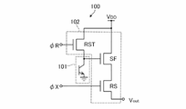
- the neutron detection element 100 has a neutron detection unit 101 that detects neutrons and converts them into an electric signal, and an amplification unit 102 that amplifies the output of the neutron detection unit.
- the amplification unit 102 has a reset transistor (RST), a source follower transistor (SF), and a row selection transistor (RS). It can be driven as a neutron detection element by adding a reset signal to ⁇ R and a row selection signal to ⁇ X.
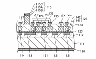
- the neutron detection unit 101 and the amplification unit 102 are formed on a p - type semiconductor layer 112 formed on an n-type semiconductor substrate 111.
- the semiconductor substrate 111 and the semiconductor layer 112 are made of silicon carbide (SiC).
- the semiconductor layer 112 is formed with an n + type detection unit diffusion layer 113, a source / drain diffusion layer 121, and a p + type potential stabilization region 114.
- a gate insulating film 123 is formed on the semiconductor layer 112, and a gate electrode 124 is formed in a predetermined region on the gate insulating film 123.
- an ohmic electrode 117 that is in ohmic contact with the potential stabilization region 114 and a source drain electrode 122 that is in ohmic contact with the source drain diffusion layer 121 are formed.
- the ohmic electrode 117 and the source / drain electrode 122 are formed by a silicide layer 141 that is in ohmic contact with the diffusion layer and a metal electrode layer 142 that covers the silicide layer 141.
- An interlayer insulating film 133 is formed on the semiconductor layer 112 so as to cover each electrode, and a neutron conversion layer 115, wiring 135, and wiring 136 are formed on the interlayer insulating film 133.
- the neutron detection unit 101 and the amplification unit 102 are formed with an amplification unit 102 having a reset transistor (RST), a source follower transistor (SF), and a row selection transistor (RS).
- RST reset transistor
- SF source follower transistor
- RS row selection transistor
- one of the source / drain diffusion layers of the reset transistor (RST) is integrally formed with the detection unit diffusion layer 113.
- a back surface electrode 126 is provided on the back surface of the semiconductor substrate 111.
- the back surface electrode 126 is an ohmic electrode that is in ohmic contact with the back surface of the semiconductor substrate 111, and can be formed of niobium-nickel silicide or the like.
- the back surface electrode 126 has the effect of rapidly discharging the electron / hole carriers generated in the semiconductor substrate 111 and stabilizing the device operation.
- the neutron conversion layer 115 is a metal film having a 10 B-containing layer 115 A containing boron 10 ( 10 B), which is an isotope of boron which is a conversion functional layer.
- the 10 B-containing layer 115 A can be formed by, for example, ion-implanting 10 B, or depositing 10 B by a sputtering method, a vapor deposition method, or the like.
- the conversion functional layer may be a layer containing lithium 6 ( 6 Li), which is an isotope of lithium, instead of the 10 B-containing layer.
- the lower metal layer 115B is present on the lower side of the 10B-containing layer 115A and the upper metal layer 115C is present on the upper side, but the upper metal layer 115C may not be present.
- the lower metal layer 115B and the upper metal layer 115C are preferably metals having a relatively large atomic number from the viewpoint of making it difficult for ⁇ rays and Li rays to pass through.
- metals having a relatively large atomic number from the viewpoint of making it difficult for ⁇ rays and Li rays to pass through.
- Al aluminum
- W tungsten
- Mo molybdenum
- Al is preferable because it can be formed by the same method as Al wiring.
- the neutrons incident on the neutron conversion layer 115 react with 10B to generate ⁇ -rays and Li particle beams.
- the lower metal layer 115B made of Al or the like, Li particle rays are more easily attenuated than ⁇ rays, and only ⁇ rays pass through the lower metal layer 115B and enter the detection unit diffusion layer 113 to detect n + type.
- An electron-hole pair is generated in the depletion layer near the PN junction between the partial diffusion layer 113 and the p-type semiconductor layer 112.
- the generated negative charge (electron) of the electron-hole pair moves to the n + type detector diffusion layer 113. This charge is accumulated in the gate electrode of the SF transistor through the wirings 135 and 136, and changes the potential of the gate electrode.
- a parasitic bipolar junction transistor (BJT) is formed. Positive charges (holes) from electron-hole pairs generated in the depletion layer are injected into the base portion of the parasitic BJT, and the parasitic BJT is temporarily turned on and diffused from the semiconductor substrate 111 through the base portion. Electrons move to layer 113. Similar to the electrons of the electron-hole pair generated in the depletion layer, the electrons are accumulated in the gate electrode of the SF transistor through the wirings 135 and 135, and the potential of the gate electrode is further changed.
- the amplification effect by the parasitic BJT can be further increased, that is, the number of electrons injected from the semiconductor substrate 111 into the detection unit diffusion layer 113 can be increased. ..
- the presence of the parasitic BJT can increase the sensitivity of the sensor.
- the parasitic BJT is not always necessary, and the sensor operates only with the detection unit diffusion layer 113.
- the charge accumulated in the gate electrode of the SF transistor changes the potential of this gate electrode, and as a result, after the RS transistor is turned on, the output voltage changes according to the potential of the gate electrode of the SF transistor. By measuring this potential, it becomes possible to measure the number of neutrons incident on the sensor.
- the detection unit diffusion layer 113 is integrated with the source / drain diffusion layer of the reset transistor (RST), and the negative charge transferred to the detection unit diffusion layer 113 is read out by the amplification unit 102 and converted into neutrons. A signal corresponding to the energy of the neutrons incident on the layer 115 is obtained.
- the positive charge (hole) is discharged through the potential stabilization region 114.
- the formation of the parasitic BJT improves the detection sensitivity of neutrons, but the configuration may be such that the parasitic BJT is not formed.
- the neutron detection element 100 of the present embodiment detects neutrons by using only ⁇ rays among ⁇ rays and Li particle beams generated by neutrons incident on the neutron conversion layer 115. Therefore, the quantification of neutrons can be improved.
- the neutron conversion layer 115 is formed only directly above the detection unit diffusion layer 113, and is not formed on the transistor or the like constituting the amplification unit 102.
- the neutron conversion layer 115 By forming the neutron conversion layer 115 only directly above the detection unit diffusion layer 113, it is difficult for ⁇ rays emitted from the neutron conversion layer 115 to enter the portion of the semiconductor layer 112 other than the detection unit diffusion layer 113. It is possible to prevent malfunctions from occurring.
- the portion directly above the detection unit diffusion layer 113 is a portion that overlaps the detection unit diffusion layer 113 in a plan view, but the detection unit diffusion layer 113 and the neutron conversion layer 115 do not have to completely overlap.
- the neutron conversion layer 115 may be formed in a portion other than directly above the detection unit diffusion layer 113.
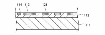
- the silicon carbide light receiving element of the present embodiment can be formed, for example, as follows. First, as shown in FIG. 3A, the p-type semiconductor layer 112 is epitaxially grown on the n-type semiconductor substrate 111. Subsequently, the n-type impurities are selectively injected into the semiconductor layer 112 using the first ion implantation mask to form the n + type detector diffusion layer 113 and the source / drain diffusion layer 121. In addition, a second ion implantation mask is used to form the p + -type potential stabilizing region 114. After this, activation annealing is performed.
- the semiconductor substrate 111 is not particularly limited, but may be 4H-SiC.
- the thickness of the semiconductor layer 112 can be, for example, about 1 ⁇ m to 5 ⁇ m.
- the first ion implantation mask and the second ion implantation mask can be formed, for example, by a silicon oxide (SiO 2 ) film.
- the activation annealing may be performed by covering the semiconductor layer 112 in which ions have been implanted with a carbon cap film and then performing a heat treatment at about 1700 ° C.
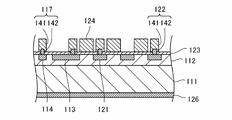
- thermal oxidation is performed to form a gate insulating film 123 having a thickness of about 20 nm, and then an ohmic electrode 117, a source / drain electrode 122, a gate electrode 124, and a back surface electrode 126 are formed.
- the ohmic electrode 117 and the source / drain electrode 122 can be formed by, for example, a silicide layer 141 and a metal electrode layer 142.
- the silicide layer 141 can be formed by selectively forming a metal film to be the silicide layer 141 by, for example, a lift-off method using a resist mask, and then silicidizing it by heat treatment.
- the metal film in this case can be, for example, a niobium-nickel film, but can also be formed of a metal forming another silicide such as a nickel-molybdenum alloy film.
- the metal electrode layer 142 can be formed by forming a metal film made of Al or the like so as to cover the silicide layer 141 and selectively removing the metal film by etching.
- the metal electrode layer 142 and the gate electrode 124 can be formed by the same process.
- the metal electrode layer 142 and the gate electrode 124 can also be formed of titanium nitride, polysilicon, or the like.
- the back surface electrode 126 may be formed by forming a metal film such as a niobium-nickel film on the back surface of the semiconductor substrate 111 and then silicidizing the back surface electrode 126.
- an interlayer insulating film 133 made of silicon oxide or the like is formed on the entire surface of the semiconductor substrate 111, and a lower metal layer 115B is formed on the interlayer insulating film 133.
- the thickness of the interlayer insulating film 133 affects the incident of ⁇ rays emitted from the neutron conversion layer 115 on the detection unit diffusion layer 113, and can be, for example, about 1 ⁇ m.
- 10 B is ion-implanted into the lower metal layer 115 B to form the 10 B-containing layer 115 A which is an impurity diffusion layer.
- the lower metal layer 115B may be any metal layer that attenuates Li particle beams, and can be formed of aluminum, tungsten, molybdenum, or the like.
- the 10B - containing layer 115A can be formed by depositing 10B by a sputtering method, a vapor deposition method, or the like, not limited to the ion implantation method.
- the thickness of the lower metal layer 115B is such that the Li particle beam does not pass through and the ⁇ ray passes through. The thickness may be appropriately determined depending on the type of metal used, and for example, it may be about 2 ⁇ m to 4 ⁇ m in the case of aluminum and about 0.4 ⁇ m in the case of tungsten.
- the implantation amount can be about 1 ⁇ 10 15 cm ⁇ 2 to about 4 ⁇ 10 15 cm ⁇ 2 .
- the thickness of the upper metal layer 115C is not particularly limited, but in the case of aluminum, for example, it can be about 10 nm to 1000 nm.
- the 6 Li-containing layer can also be formed in the same manner.
- the lower metal layer 115B on which the 10B-containing layer 115A is formed is selectively removed except immediately above the detection unit diffusion layer 113.
- the upper metal layer 115C, the wiring 135, and the wiring 136 are formed. If the upper metal layer 115C and the wiring 135 and the wiring 136 are made of the same metal, they can be formed by the same process.
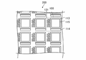
- the neutron detection element 100 of the present embodiment can be arranged in a matrix as shown in FIG. 4 to form a neutron two-dimensional sensor 200 having the neutron detection element 100 as one pixel.
- the neutron two-dimensional sensor 200 By using the neutron two-dimensional sensor 200, the distribution on the plane of neutrons can be easily measured, and the transmission and absorption of neutrons can be evaluated in real time in neutron radiography and BNCT. Further, since the neutron detection element 100 of the present embodiment is excellent in quantification, it is possible to visualize the intensity distribution of neutrons with high accuracy.
- a high-density layer 151 can be formed between the neutron conversion layer 115 and the detection unit diffusion layer 113.
- the high-density layer 151 may be a layer having a higher density than the semiconductor layer 112, and a layer containing a metal is preferable.
- a simple metal layer, an alloy layer containing a plurality of metals, a silicide layer, and other metals and non-metals Can be a layer containing.
- the high-density layer is formed by the same silicide layer as the source-drain electrode 122, the high-density layer can be formed without increasing the number of steps. In this case, the silicide layer 141 of the source / drain electrode 122 and the high-density layer 151 can be integrally formed.
- the high-density layer 151 is preferably in contact with the detection unit diffusion layer 113, but it may also have a configuration in which another layer such as an insulating film exists between the high-density layer 151 and the detection unit diffusion layer 113. ..
- the high-density layer 151 is preferably formed at least directly below the neutron conversion layer 115 in the detection unit diffusion layer 113. It may be formed so as to cover the entire detection unit diffusion layer 113, or it may be formed so as to cover a wider area than the detection unit diffusion layer 113.
- the thickness of the high-density layer 115 is not particularly limited, but it is preferably about 0.01 ⁇ m to 0.3 ⁇ m from the viewpoint of preventing ⁇ rays from reaching the detection unit diffusion layer and preventing penetration.
- the high-density layer 151 is formed by the same process as the silicide layer 141 of the source / drain electrode 122, the thickness can be matched with the silicide layer 141 of the source / drain electrode 122.
- the semiconductor layer 112 is a p-type, and an n-type transistor is formed.
- the semiconductor layer 112 may be n-type, and a p-type detection unit diffusion layer and a transistor may be formed.
- the potential stabilization region can be n + type.
- the potential stabilization region may or may not be provided as needed.
- the potential stabilization region 114 is arranged so as to be separated from and adjacent to the detection unit diffusion layer 113.
- the effect of stabilizing the potential can be further enhanced.
- the potential stabilization region 114 can be formed on any of the same semiconductor layers 112 as the detection unit diffusion layer 113.
- the + sign attached to the p or n symbol indicating the conductive type indicates that the impurity concentration is higher than in the case where no sign is attached, and the-sign indicates that the impurity concentration is higher than in the case where no sign is attached. Indicates that the impurity concentration is low.
- the element can also be formed of a silicon semiconductor.
- the neutron detection element of the present disclosure is particularly useful in the medical field using neutrons because output fluctuation is unlikely to occur and quantitative detection of neutrons is easy.
- Neutral detection element 101 Neutral detection unit 102 Amplification unit 111 Semiconductor substrate 112 Semiconductor layer 113 Detection unit Diffusion layer 114 Potential stabilization region 115 Neutron conversion layer 115A 10 B-containing layer 115B Lower metal layer 115C Upper metal layer 117 Ohmic electrode 121 Source Drain diffusion layer 122 Source drain electrode 123 Gate insulating film 124 Gate electrode 126 Backside electrode 133 Interlayer insulating film 135 Wiring 136 Wiring 141 silicide layer 142 Metal electrode layer 151 High density layer 200 Neutron two-dimensional sensor
Landscapes
- Physics & Mathematics (AREA)
- Health & Medical Sciences (AREA)
- Life Sciences & Earth Sciences (AREA)
- General Physics & Mathematics (AREA)
- High Energy & Nuclear Physics (AREA)
- Molecular Biology (AREA)
- Spectroscopy & Molecular Physics (AREA)
- Measurement Of Radiation (AREA)
- Light Receiving Elements (AREA)
Abstract
Description
101 中性子検出部
102 増幅部
111 半導体基板
112 半導体層
113 検出部拡散層
114 電位安定化領域
115 中性子変換層
115A 10B含有層
115B 下側金属層
115C 上側金属層
117 オーミック電極
121 ソースドレイン拡散層
122 ソースドレイン電極
123 ゲート絶縁膜
124 ゲート電極
126 裏面電極
133 層間絶縁膜
135 配線
136 配線
141 シリサイド層
142 金属電極層
151 高密度層
200 中性子2次元センサ
Claims (8)
- 中性子を検出して電気信号に変換する中性子検出部と、
前記中性子検出部の出力を増幅する増幅部とを備え、
前記中性子検出部は、第1導電型の半導体層と、前記半導体層に形成された第2導電型の検出部拡散層と、前記検出部拡散層の上に形成された中性子をα線に変換する中性子変換層とを有し、
前記増幅部は、前記半導体層に形成された複数のトランジスタとを有し、
前記中性子変換層は、ホウ素10を含む層又はリチウム6を含む層を有する金属膜である、中性子検出素子。 - 前記ホウ素10を含む層又はリチウム6を含む層は、不純物拡散層である、請求項1に記載の中性子検出素子。
- 前記半導体層は、炭化珪素半導体層である、請求項1又は2に記載の中性子検出素子。
- 前記中性子変換層は、前記検出部拡散層の直上に絶縁膜を介して形成されている、請求項1~3のいずれか1項に記載の中性子検出素子。
- 前記中性子変換層と前記検出部拡散層との間に形成され、前記半導体層よりも密度が高い材料により形成された、高密度層を有している、請求項1~4のいずれか1項に記載の中性子検出素子。
- 前記高密度層は、金属シリサイド層である、請求項5に記載の中性子検出素子。
- 前記半導体層に形成され、前記半導体層よりも不純物濃度が高い第1導電型の電位安定化領域を有している、請求項1~6のいずれか1項に記載の中性子検出素子。
- 請求項1~7のいずれか1項に記載の中性子検出素子がマトリクス状に配置された、中性子2次元センサ。
Priority Applications (2)
| Application Number | Priority Date | Filing Date | Title |
|---|---|---|---|
| US18/266,601 US12416737B2 (en) | 2020-12-11 | 2021-12-01 | Neutron detection element |
| JP2022568215A JP7843499B2 (ja) | 2020-12-11 | 2021-12-01 | 中性子検出素子 |
Applications Claiming Priority (2)
| Application Number | Priority Date | Filing Date | Title |
|---|---|---|---|
| JP2020-205664 | 2020-12-11 | ||
| JP2020205664 | 2020-12-11 |
Publications (1)
| Publication Number | Publication Date |
|---|---|
| WO2022124155A1 true WO2022124155A1 (ja) | 2022-06-16 |
Family
ID=81973580
Family Applications (1)
| Application Number | Title | Priority Date | Filing Date |
|---|---|---|---|
| PCT/JP2021/044054 Ceased WO2022124155A1 (ja) | 2020-12-11 | 2021-12-01 | 中性子検出素子 |
Country Status (3)
| Country | Link |
|---|---|
| US (1) | US12416737B2 (ja) |
| JP (1) | JP7843499B2 (ja) |
| WO (1) | WO2022124155A1 (ja) |
Families Citing this family (1)
| Publication number | Priority date | Publication date | Assignee | Title |
|---|---|---|---|---|
| TWI838103B (zh) * | 2023-01-31 | 2024-04-01 | 禾榮科技股份有限公司 | 中子量測方法及中子量測裝置 |
Citations (5)
| Publication number | Priority date | Publication date | Assignee | Title |
|---|---|---|---|---|
| JPH07176777A (ja) * | 1993-12-20 | 1995-07-14 | Hitachi Ltd | 中性子検出器及び中性子モニタ |
| WO2013002697A1 (en) * | 2011-06-30 | 2013-01-03 | European Spallation Source Ess Ab | A method for producing a neutron detector component comprising a boron carbide layer for use in a neutron detecting device |
| JP2016535240A (ja) * | 2014-07-14 | 2016-11-10 | ヘルムホルツ−ツェントルム ゲーストハハト ツェントルム フュアー マテリアル ウント キュステンフォルシュンク ゲーエムベーハー | 中性子コンバータの製造方法 |
| JP2018017613A (ja) * | 2016-07-28 | 2018-02-01 | 日立Geニュークリア・エナジー株式会社 | 放射線計測装置 |
| JP2018505396A (ja) * | 2014-12-19 | 2018-02-22 | コミッサリア ア レネルジー アトミーク エ オ ゼネルジ ザルタナテイヴ | 中性子検出器を実現するための方法及び中性子検出器 |
Family Cites Families (6)
| Publication number | Priority date | Publication date | Assignee | Title |
|---|---|---|---|---|
| US5940460A (en) * | 1997-09-15 | 1999-08-17 | The United States Of America As Represented By The United States Department Of Energy | Solid state neutron detector array |
| US7902513B2 (en) * | 2008-03-19 | 2011-03-08 | The United States Of America As Represented By The Secretary Of The Navy | Neutron detector with gamma ray isolation |
| JP2012181065A (ja) | 2011-02-28 | 2012-09-20 | High Energy Accelerator Research Organization | 放射線検出装置 |
| US20140027648A1 (en) | 2011-09-22 | 2014-01-30 | Sture Petersson | Neutron Detector |
| WO2015015700A1 (ja) * | 2013-08-02 | 2015-02-05 | シャープ株式会社 | 放射線検出用半導体装置 |
| JP6948668B2 (ja) | 2017-02-28 | 2021-10-13 | 国立大学法人静岡大学 | 中性子半導体検出器 |
-
2021
- 2021-12-01 JP JP2022568215A patent/JP7843499B2/ja active Active
- 2021-12-01 US US18/266,601 patent/US12416737B2/en active Active
- 2021-12-01 WO PCT/JP2021/044054 patent/WO2022124155A1/ja not_active Ceased
Patent Citations (5)
| Publication number | Priority date | Publication date | Assignee | Title |
|---|---|---|---|---|
| JPH07176777A (ja) * | 1993-12-20 | 1995-07-14 | Hitachi Ltd | 中性子検出器及び中性子モニタ |
| WO2013002697A1 (en) * | 2011-06-30 | 2013-01-03 | European Spallation Source Ess Ab | A method for producing a neutron detector component comprising a boron carbide layer for use in a neutron detecting device |
| JP2016535240A (ja) * | 2014-07-14 | 2016-11-10 | ヘルムホルツ−ツェントルム ゲーストハハト ツェントルム フュアー マテリアル ウント キュステンフォルシュンク ゲーエムベーハー | 中性子コンバータの製造方法 |
| JP2018505396A (ja) * | 2014-12-19 | 2018-02-22 | コミッサリア ア レネルジー アトミーク エ オ ゼネルジ ザルタナテイヴ | 中性子検出器を実現するための方法及び中性子検出器 |
| JP2018017613A (ja) * | 2016-07-28 | 2018-02-01 | 日立Geニュークリア・エナジー株式会社 | 放射線計測装置 |
Also Published As
| Publication number | Publication date |
|---|---|
| JP7843499B2 (ja) | 2026-04-10 |
| US20240045087A1 (en) | 2024-02-08 |
| US12416737B2 (en) | 2025-09-16 |
| JPWO2022124155A1 (ja) | 2022-06-16 |
Similar Documents
| Publication | Publication Date | Title |
|---|---|---|
| CN101281148B (zh) | 一种高分辨率的半导体核辐射探测器 | |
| Bolotnikov et al. | Factors limiting the performance of CdZnTe detectors | |
| US20100148040A1 (en) | Geiger-mode photodiode with integrated and adjustable quenching resistor, photodiode array, and manufacturing method thereof | |
| JP2004080010A (ja) | 直接変換に基づく画像化x線検出器 | |
| US12183844B2 (en) | Radiation detection element, radiation detector and radiation detection device | |
| JP2013021014A (ja) | エネルギー線検出装置の製造方法 | |
| TW202118077A (zh) | 半導體本體、累崩式光二極體以及半導體本體之製造方法 | |
| US7847360B2 (en) | Radiation detector of the deltaE-E type with insulation trenches | |
| US12416737B2 (en) | Neutron detection element | |
| Iwanczyk et al. | Simulation and modelling of a new silicon X-ray drift detector design for synchrotron radiation applications | |
| US6172370B1 (en) | Lateral PN arrayed digital x-ray image sensor | |
| EP2888764B1 (en) | Photon counting semiconductor detectors | |
| US9159765B2 (en) | Apparatus for detecting soft X-ray radiation and X-ray detection system including such apparatus | |
| Arnab et al. | A novel amorphous selenium avalanche detector structure for low dose medical X-ray imaging | |
| JP2023543735A (ja) | 低侵入性粒子低利得アバランシェ検出器 | |
| Hammig et al. | Suppression of interface-induced noise by the control of electron-phonon interactions | |
| EP2579067B1 (en) | X-ray detection apparatus and X-ray detection system | |
| Giubilato et al. | LePix—A high resistivity, fully depleted monolithic pixel detector | |
| RU2427942C1 (ru) | Интегральная ячейка детектора излучения на основе биполярного транзистора с сетчатой базой | |
| US20230171976A1 (en) | Imaging device and imaging method | |
| RU2583857C1 (ru) | Биполярная ячейка координатного фотоприемника - детектора излучений | |
| EP4379427A1 (en) | Silicon carbide dosimeter for high dose pulsed radiation | |
| US20250151425A1 (en) | Apparatus and method | |
| Stavro | Development of an Amorphous Selenium Based Photon Counting Detector for Breast Imaging Applications | |
| Shin et al. | Optimizing floating guard ring designs for FASPAX N-in-P silicon sensors |
Legal Events
| Date | Code | Title | Description |
|---|---|---|---|
| 121 | Ep: the epo has been informed by wipo that ep was designated in this application |
Ref document number: 21903259 Country of ref document: EP Kind code of ref document: A1 |
|
| DPE1 | Request for preliminary examination filed after expiration of 19th month from priority date (pct application filed from 20040101) | ||
| ENP | Entry into the national phase |
Ref document number: 2022568215 Country of ref document: JP Kind code of ref document: A |
|
| WWE | Wipo information: entry into national phase |
Ref document number: 18266601 Country of ref document: US |
|
| NENP | Non-entry into the national phase |
Ref country code: DE |
|
| 122 | Ep: pct application non-entry in european phase |
Ref document number: 21903259 Country of ref document: EP Kind code of ref document: A1 |
|
| WWG | Wipo information: grant in national office |
Ref document number: 18266601 Country of ref document: US |