WO2022124139A1 - 固体撮像装置、調整方法及び電子機器 - Google Patents
固体撮像装置、調整方法及び電子機器 Download PDFInfo
- Publication number
- WO2022124139A1 WO2022124139A1 PCT/JP2021/043863 JP2021043863W WO2022124139A1 WO 2022124139 A1 WO2022124139 A1 WO 2022124139A1 JP 2021043863 W JP2021043863 W JP 2021043863W WO 2022124139 A1 WO2022124139 A1 WO 2022124139A1
- Authority
- WO
- WIPO (PCT)
- Prior art keywords
- pixel
- solid
- semiconductor substrate
- state image
- charge
- Prior art date
- Legal status (The legal status is an assumption and is not a legal conclusion. Google has not performed a legal analysis and makes no representation as to the accuracy of the status listed.)
- Ceased
Links
Images












Classifications
-
- H—ELECTRICITY
- H04—ELECTRIC COMMUNICATION TECHNIQUE
- H04N—PICTORIAL COMMUNICATION, e.g. TELEVISION
- H04N25/00—Circuitry of solid-state image sensors [SSIS]; Control thereof
- H04N25/60—Noise processing, e.g. detecting, correcting, reducing or removing noise
- H04N25/62—Detection or reduction of noise due to excess charges produced by the exposure, e.g. smear, blooming, ghost image, crosstalk or leakage between pixels
-
- H—ELECTRICITY
- H04—ELECTRIC COMMUNICATION TECHNIQUE
- H04N—PICTORIAL COMMUNICATION, e.g. TELEVISION
- H04N25/00—Circuitry of solid-state image sensors [SSIS]; Control thereof
- H04N25/70—SSIS architectures; Circuits associated therewith
-
- H—ELECTRICITY
- H10—SEMICONDUCTOR DEVICES; ELECTRIC SOLID-STATE DEVICES NOT OTHERWISE PROVIDED FOR
- H10D—INORGANIC ELECTRIC SEMICONDUCTOR DEVICES
- H10D84/00—Integrated devices formed in or on semiconductor substrates that comprise only semiconducting layers, e.g. on Si wafers or on GaAs-on-Si wafers
-
- H—ELECTRICITY
- H10—SEMICONDUCTOR DEVICES; ELECTRIC SOLID-STATE DEVICES NOT OTHERWISE PROVIDED FOR
- H10D—INORGANIC ELECTRIC SEMICONDUCTOR DEVICES
- H10D84/00—Integrated devices formed in or on semiconductor substrates that comprise only semiconducting layers, e.g. on Si wafers or on GaAs-on-Si wafers
- H10D84/01—Manufacture or treatment
-
- H—ELECTRICITY
- H10—SEMICONDUCTOR DEVICES; ELECTRIC SOLID-STATE DEVICES NOT OTHERWISE PROVIDED FOR
- H10D—INORGANIC ELECTRIC SEMICONDUCTOR DEVICES
- H10D84/00—Integrated devices formed in or on semiconductor substrates that comprise only semiconducting layers, e.g. on Si wafers or on GaAs-on-Si wafers
- H10D84/01—Manufacture or treatment
- H10D84/0123—Integrating together multiple components covered by H10D12/00 or H10D30/00, e.g. integrating multiple IGBTs
- H10D84/0126—Integrating together multiple components covered by H10D12/00 or H10D30/00, e.g. integrating multiple IGBTs the components including insulated gates, e.g. IGFETs
-
- H—ELECTRICITY
- H10—SEMICONDUCTOR DEVICES; ELECTRIC SOLID-STATE DEVICES NOT OTHERWISE PROVIDED FOR
- H10D—INORGANIC ELECTRIC SEMICONDUCTOR DEVICES
- H10D84/00—Integrated devices formed in or on semiconductor substrates that comprise only semiconducting layers, e.g. on Si wafers or on GaAs-on-Si wafers
- H10D84/01—Manufacture or treatment
- H10D84/02—Manufacture or treatment characterised by using material-based technologies
- H10D84/03—Manufacture or treatment characterised by using material-based technologies using Group IV technology, e.g. silicon technology or silicon-carbide [SiC] technology
- H10D84/038—Manufacture or treatment characterised by using material-based technologies using Group IV technology, e.g. silicon technology or silicon-carbide [SiC] technology using silicon technology, e.g. SiGe
-
- H—ELECTRICITY
- H10—SEMICONDUCTOR DEVICES; ELECTRIC SOLID-STATE DEVICES NOT OTHERWISE PROVIDED FOR
- H10D—INORGANIC ELECTRIC SEMICONDUCTOR DEVICES
- H10D84/00—Integrated devices formed in or on semiconductor substrates that comprise only semiconducting layers, e.g. on Si wafers or on GaAs-on-Si wafers
- H10D84/80—Integrated devices formed in or on semiconductor substrates that comprise only semiconducting layers, e.g. on Si wafers or on GaAs-on-Si wafers characterised by the integration of at least one component covered by groups H10D12/00 or H10D30/00, e.g. integration of IGFETs
- H10D84/82—Integrated devices formed in or on semiconductor substrates that comprise only semiconducting layers, e.g. on Si wafers or on GaAs-on-Si wafers characterised by the integration of at least one component covered by groups H10D12/00 or H10D30/00, e.g. integration of IGFETs of only field-effect components
- H10D84/83—Integrated devices formed in or on semiconductor substrates that comprise only semiconducting layers, e.g. on Si wafers or on GaAs-on-Si wafers characterised by the integration of at least one component covered by groups H10D12/00 or H10D30/00, e.g. integration of IGFETs of only field-effect components of only insulated-gate FETs [IGFET]
-
- H—ELECTRICITY
- H10—SEMICONDUCTOR DEVICES; ELECTRIC SOLID-STATE DEVICES NOT OTHERWISE PROVIDED FOR
- H10F—INORGANIC SEMICONDUCTOR DEVICES SENSITIVE TO INFRARED RADIATION, LIGHT, ELECTROMAGNETIC RADIATION OF SHORTER WAVELENGTH OR CORPUSCULAR RADIATION
- H10F30/00—Individual radiation-sensitive semiconductor devices in which radiation controls the flow of current through the devices, e.g. photodetectors
- H10F30/20—Individual radiation-sensitive semiconductor devices in which radiation controls the flow of current through the devices, e.g. photodetectors the devices having potential barriers, e.g. phototransistors
-
- H—ELECTRICITY
- H10—SEMICONDUCTOR DEVICES; ELECTRIC SOLID-STATE DEVICES NOT OTHERWISE PROVIDED FOR
- H10F—INORGANIC SEMICONDUCTOR DEVICES SENSITIVE TO INFRARED RADIATION, LIGHT, ELECTROMAGNETIC RADIATION OF SHORTER WAVELENGTH OR CORPUSCULAR RADIATION
- H10F39/00—Integrated devices, or assemblies of multiple devices, comprising at least one element covered by group H10F30/00, e.g. radiation detectors comprising photodiode arrays
- H10F39/10—Integrated devices
- H10F39/12—Image sensors
Definitions
- This disclosure relates to a solid-state image sensor, an adjustment method, and an electronic device.
- CMOS Complementary MOS
- MOS Metal-Oxide-Semiconductor
- the solid-state image sensor has a feature that an active structure having an amplification function for each pixel can be easily created by a miniaturization technique associated with a CMOS process.
- peripheral circuits such as a drive circuit for driving a pixel array unit, which is an aggregate of pixels, and a signal processing circuit for processing signals output from each pixel of the pixel array unit are referred to as a pixel array unit. It has the feature that it can be integrated on the same semiconductor substrate (chip). Due to these characteristics, CMOS type solid-state image sensors are being actively developed.
- a photoelectric conversion unit that converts light into electric charge
- a charge storage unit that transfers the electric charge from the photoelectric conversion unit
- an overflow path that discharges the excess electric charge
- a solid-state imaging device comprising an adjusting circuit for adjusting the potential barrier of the overflow path.
- a photoelectric conversion unit that converts light into electric charge a charge storage unit that transfers the electric charge from the photoelectric conversion unit, and an overflow unit that discharges the excess electric charge are provided on the semiconductor substrate.
- a photoelectric conversion unit that converts light into electric charge
- a charge storage unit that transfers the electric charge from the photoelectric conversion unit
- an overflow unit that discharges the excess electric charge
- An electronic device comprises a solid-state imaging device comprising a path and an adjustment circuit that adjusts the potential barrier of the overflow path.
- FIG. 1 It is sectional drawing which shows an example of the detailed structure of the pixel 100 which concerns on 4th Embodiment of this disclosure. It is a plane schematic diagram which shows an example of the detailed structure of the pixel 100 which concerns on 5th Embodiment of this disclosure. It is sectional drawing which shows an example of the detailed structure of the pixel 100 which concerns on 5th Embodiment of this disclosure. It is sectional drawing which shows an example of the detailed structure of the pixel 100 which concerns on 6th Embodiment of this disclosure. It is a plane schematic diagram which shows an example of the detailed structure of the pixel 100 which concerns on 7th Embodiment of this disclosure. It is sectional drawing which shows an example of the detailed structure of the pixel 100 which concerns on 7th Embodiment of this disclosure. FIG.
- FIG. 1 is a schematic plan view (No. 1) showing an example of the detailed configuration of the pixel array unit 30 according to the seventh embodiment of the present disclosure.
- FIG. 2 is a schematic plan view (No. 2) showing an example of the detailed configuration of the pixel array unit 30 according to the seventh embodiment of the present disclosure.
- It is an equivalent circuit diagram of the pixel 100 which concerns on 8th Embodiment of this disclosure.
- It is a plane schematic diagram which shows an example of the detailed structure of the pixel 100 which concerns on 8th Embodiment of this disclosure.
- a plurality of components having substantially the same or similar functional configurations may be distinguished by adding different numbers after the same reference numerals. However, if it is not necessary to particularly distinguish each of the plurality of components having substantially the same or similar functional configurations, only the same reference numerals are given. Further, similar components of different embodiments may be distinguished by adding different alphabets after the same reference numerals. However, if it is not necessary to distinguish each of the similar components, only the same reference numerals are given.
- the drawings referred to in the following description are drawings for explaining and understanding one embodiment of the present disclosure, and for the sake of clarity, the shapes, dimensions, ratios, etc. shown in the drawings are actually shown. May differ from.
- the image pickup apparatus shown in the figure can be appropriately redesigned in consideration of the following description and known techniques.
- the vertical direction of the laminated structure of the image pickup device corresponds to the relative direction when the light receiving surface on which the light incident on the image pickup device enters is facing down. It may differ from the vertical direction according to the actual gravitational acceleration.
- the embodiment of the present disclosure is applied to a back-illuminated image pickup apparatus. Therefore, in the image pickup apparatus, light is incident from the back surface side of the substrate. .. Therefore, in the following description, the front surface of the substrate is the surface facing the back surface when the side on which light is incident is the back surface.
- electrically connected means connecting a plurality of elements so that electricity (signal) is conducted. Means that.
- electrically connected in the following description includes not only the case of directly and electrically connecting a plurality of elements, but also indirectly and electrically through other elements. It shall also include the case of connecting to.
- FIG. 1 is an explanatory diagram showing a plan configuration example of the image pickup apparatus 1 according to the embodiment of the present disclosure.
- the image pickup apparatus 1 according to the embodiment of the present disclosure includes, for example, a pixel array unit 30 in which a plurality of pixels 100 are arranged in a matric manner on a semiconductor substrate 10 made of silicon, and the pixels. It has a peripheral circuit unit provided so as to surround the array unit 30.
- the image pickup apparatus 1 includes a vertical drive circuit unit 32, a column signal processing circuit unit 34, a horizontal drive circuit unit 36, an output circuit unit 38, a control circuit unit 40, and the like as the peripheral circuit unit. The details of each block of the image pickup apparatus 1 will be described below.
- the pixel array unit 30 has a plurality of pixels 100 arranged two-dimensionally in a matrix along the row direction and the column direction on the semiconductor substrate 10.
- Each pixel 100 has a photodiode (photoelectric conversion unit) (not shown) that performs photoelectric conversion on incident light to generate an electric charge, and a plurality of pixel transistors (for example, a MOS (Metal-Oxide-Semiconductor) transistor).
- the pixel transistor includes, for example, four MOS transistors such as a transfer transistor, a selection transistor, a reset transistor, and an amplification transistor.
- a plurality of pixels 100 are arranged two-dimensionally according to, for example, a Bayer arrangement.
- pixels 100 that absorb light having a green wavelength (for example, a wavelength of 495 nm to 570 nm) and generate a charge are arranged in a checkered pattern, and the remaining portion has a red wavelength (for example, a wavelength of 620 nm or more).
- a pixel 100 that absorbs light having a wavelength of 750 nm and generates a charge and a pixel 100 that absorbs light having a blue wavelength (for example, a wavelength of 450 nm to 495 nm) and generates a charge are arranged alternately in a row.
- An array pattern The detailed structure of the pixel 100 will be described later.
- the vertical drive circuit unit 32 is formed by, for example, a shift register, selects a pixel drive wiring 42, supplies a pulse for driving the pixel 100 to the selected pixel drive wiring 42, and drives the pixel 100 in row units. .. That is, the vertical drive circuit unit 32 selectively scans each pixel 100 of the pixel array unit 30 in the vertical direction (vertical direction in FIG. 1) in a row-by-row manner, and receives light from the photoelectric conversion unit (not shown) of each pixel 100. A pixel signal based on the signal charge generated according to the amount is supplied to the column signal processing circuit unit 34 described later through the vertical signal line 44.
- the column signal processing circuit unit 34 is arranged for each column of the pixel 100, and performs signal processing such as noise removal for each pixel signal for the pixel signal output from the pixel 100 for one row.
- the column signal processing circuit unit 34 performs signal processing such as CDS (Correlated Double Sampling) and AD (Analog-Degital) conversion in order to remove fixed pattern noise peculiar to pixels.
- the horizontal drive circuit unit 36 is formed by, for example, a shift register, and by sequentially outputting horizontal scan pulses, each of the above-mentioned column signal processing circuit units 34 is sequentially selected, and pixels from each of the column signal processing circuit units 34. The signal is output to the horizontal signal line 46.
- the output circuit unit 38 performs signal processing on the pixel signals sequentially supplied from each of the column signal processing circuit units 34 described above through the horizontal signal line 46, and outputs the signals.
- the output circuit unit 38 may function as, for example, a functional unit that performs buffering, or may perform processing such as black level adjustment, column variation correction, and various digital signal processing. Note that buffering refers to temporarily storing pixel signals in order to compensate for differences in processing speed and transfer speed when exchanging pixel signals.
- the input / output terminal 48 is a terminal for exchanging signals with an external device.
- Control circuit unit 40 receives an input clock and data instructing an operation mode or the like, and outputs data such as internal information of the image pickup apparatus 1. That is, the control circuit unit 40 is based on the vertical synchronization signal, the horizontal synchronization signal, and the master clock, and is a clock signal that serves as a reference for the operation of the vertical drive circuit unit 32, the column signal processing circuit unit 34, the horizontal drive circuit unit 36, and the like. Generate a control signal. Then, the control circuit unit 40 outputs the generated clock signal and control signal to the vertical drive circuit unit 32, the column signal processing circuit unit 34, the horizontal drive circuit unit 36, and the like.
- CMOS type solid-state image sensor that can be manufactured by the same process as the MOS integrated circuit can be applied to the image pickup device 1 as the pixel 100.
- the solid-state image sensor has a feature that an active structure having an amplification function can be easily created for each pixel 100 by the miniaturization technique associated with the CMOS process.
- the solid-state image sensor has the same peripheral circuit units as the pixel array unit 30, such as a drive circuit for driving the pixel array unit 30 and a signal processing circuit for processing signals output from each pixel 100 of the pixel array unit 30. It has a feature that it can be integrated on a semiconductor substrate (chip) 10. Due to these characteristics, CMOS type solid-state image sensors are being actively developed.
- the overflow path is independent of the transfer design.
- a structure capable of controlling the potential of the potential barrier can be mentioned.
- an n-type semiconductor region-p-type semiconductor region-n-type semiconductor region is formed along the film thickness direction of the semiconductor substrate 10.
- the present inventor provides an overflow path on the photodiode independently of the gate of the transfer transistor, and further, individually by biasing to apply the potential of the potential barrier of the overflow path.
- the saturation signal amount is measured in advance for each image pickup device 1, wafer, or lot, and the bias value to be applied is determined based on the measurement result. By doing so, the bias applied to the overflow path can be determined in consideration of the variation in the potential of the potential barrier of the overflow path.
- the saturation signal amount decreases or the excess charge becomes difficult to be discharged due to the variation in the potential of the potential barrier of the overflow path, and the yield decreases. Can be avoided.
- the overflow path is provided on the photodiode independently of the gate of the transfer transistor, it is possible to improve other characteristics of the pixel 100.
- FIG. 2 is an equivalent circuit diagram of the pixel 100 according to the present embodiment.
- the pixel 100 has a photodiode PD as a photoelectric conversion element (photoelectric conversion unit) that converts light into electric charges, and a charge discharge transistor OF. Further, the pixel 100 has a transfer transistor TG, a stray diffusion region FD, a reset transistor RST, an amplification transistor AMP, and a selection transistor SEL.
- one of the source / drain of the charge discharge transistor OF is electrically connected to the photodiode PD that generates charge by receiving light. Further, the other of the source / drain of the charge discharge transistor OF is electrically connected to the power supply circuit (power supply potential VDD). Then, the charge discharge transistor OF can discharge excess charge from the photodiode PD to the power supply circuit (power supply potential VDD) according to the voltage applied to its own gate.
- one of the source / drain of the transfer transistor TG is electrically connected to the photodiode PD, and the other of the source / drain of the transfer transistor TG is the floating diffusion region FD. Is electrically connected to. Then, the transfer transistor TG becomes conductive according to the voltage applied to its own gate, and the electric charge generated by the photodiode PD can be transferred to the stray diffusion region FD.
- the floating diffusion region FD is electrically connected to the gate of the amplification transistor AMP that converts the electric charge into a voltage and outputs it as a signal.
- one of the source / drain of the amplification transistor AMP is electrically connected to one of the source / drain of the selection transistor that outputs the signal obtained by conversion to the signal line according to the selection signal.
- the other of the source / drain of the amplification transistor AMP is electrically connected to the power supply circuit (power supply potential VDD).
- the other of the source / drain of the selection transistor SEL is electrically connected to the signal line that transmits the converted voltage as a signal, and is further electrically connected to the column signal processing circuit unit 34 described above.
- the gate of the selection transistor SEL is electrically connected to a selection line (not shown) for selecting a line for outputting a signal, and further electrically connected to the above-mentioned vertical drive circuit unit 32. That is, the electric charge accumulated in the floating diffusion region FD is converted into a voltage by the amplification transistor AMP2 under the control of the selection transistor SEL, and is output to the signal line.
- the floating diffusion region FD is electrically connected to one of the drain / source of the reset transistor RST for resetting the accumulated charge.
- the gate of the reset transistor RST is electrically connected to a reset signal line (not shown), and further electrically connected to the above-mentioned vertical drive circuit unit 32.
- the other of the drain / source of the reset transistor RST is electrically connected to the power supply circuit (power supply potential VDD). Then, the reset transistor RST becomes conductive according to the voltage applied to its own gate, and the electric charge accumulated in the stray diffusion region FD can be reset (discharged to the power supply circuit (power supply potential VDD)).
- the equivalent circuit of the pixel 100 according to the present embodiment is not limited to the example shown in FIG. 2, and may include, for example, other elements and the like, and is not particularly limited.
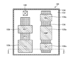
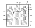
- FIG. 3 is a schematic plan view showing an example of the detailed configuration of the pixel 100 according to the present embodiment, and is a view when the pixel 100 is viewed from above the surface of the semiconductor substrate 102.
- a pixel separation portion 104 made of an insulating film embedded in a groove provided in the semiconductor substrate 102 is provided so as to surround the outer periphery of the pixel 100.
- the p-type (second conductive type) semiconductor substrate 102 surrounded by the pixel separation portion 104 is provided with an n-type (first conductive type) semiconductor region 106.
- a charge discharge transistor OF, a transfer transistor TG, a reset transistor RST, an amplification transistor AMP, and gate electrodes 108o, 108t, 108r of the selection transistor SEL are placed on the semiconductor substrate 102 via an oxide insulating film (not shown). 108a and 108s are provided.
- the gate electrodes 108t and 108r of the transfer transistor TG and the reset transistor RST are arranged along the vertical direction in the figure, and the gate electrode 108t and the gate electrode 108r are arranged in a plan view.
- the n-type semiconductor region located between them functions as a floating diffusion region FD for accumulating charges.
- the gate electrodes 108o, 108a, 108s of the charge discharge transistor OF, the amplification transistor AMP, and the selection transistor SEL are arranged along the vertical direction in the figure, and are sandwiched between the gate electrodes 108o, 108a, 108s in a plan view.
- the n-type semiconductor region is used as a source or drain of these transistors.
- the p-type semiconductor substrate 102 surrounded by the pixel separation portion 104 is provided with a contact 140 for setting the p-well region (not shown) of the p-type semiconductor substrate to a predetermined potential.
- planar structure of the pixel 100 according to the present embodiment is not limited to the example shown in FIG. 3, and may include, for example, other elements and the like, and is not particularly limited.
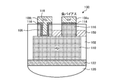
- FIG. 4 is a schematic cross-sectional view showing an example of the detailed configuration of the pixel 100 according to the present embodiment.
- FIG. 4 is a cross-sectional view when the pixel 100 is cut along the line AA'of FIG. 3, and in detail, the lower side in FIG. 4 is the back surface side of the semiconductor substrate 102. The upper side of 4 is the surface side of the semiconductor substrate 102.
- the pixel 100 has a semiconductor substrate 102 made of a silicon substrate or the like. Specifically, a p-type semiconductor region (not shown) and an n-type semiconductor region (not shown) are laminated in the semiconductor substrate 102, whereby a photodiode (PD) (photoelectric conversion unit) is formed in the semiconductor substrate 102. 110 is formed.
- the photodiode 110 performs photoelectric conversion by light incident from the back surface of the semiconductor substrate 102 to generate electric charges.
- a p-type separation layer 150 is provided above the photodiode 110.
- the p-type separation layer 150 has a function of separating the n-type semiconductor region (not shown) of the photodiode 110 and the n-type diffusion region (not shown) of the pixel transistor.
- an on-chip lens 120 made of a styrene resin, an acrylic resin, a styrene-acrylic copolymer resin, a siloxane resin, or the like, which is incident with light, is provided.
- a pixel separation unit 104 is provided so as to surround the pixel 100 so as to penetrate the semiconductor substrate 102 and prevent incident light from entering the adjacent pixel 100.
- the pixel separation portion 104 is composed of, for example, a trench penetrating from the back surface to the front surface or from the front surface to the back surface of the semiconductor substrate 200, and an insulating film such as silicon oxide embedded in the trench.
- a gate electrode (transfer gate) 108t of the transfer transistor TG Adjacent to the photodiode 110, a gate electrode (transfer gate) 108t of the transfer transistor TG is provided on the surface of the semiconductor substrate 102.
- the gate electrode 108t is, for example, made of a polysilicon film and has an embedded portion 118 embedded in an n-type semiconductor region 106 of a semiconductor substrate 102 via an insulating film 114 and a p-type semiconductor region (not shown). It has a type gate electrode structure. Further, a floating diffusion region (FD) (charge storage portion) (see FIG.
- FD floating diffusion region
- a gate electrode (overflow gate) 108o of the charge discharge transistor OF is provided on the surface of the semiconductor substrate 102.
- the gate electrode 108o is a vertical type having, for example, a polysilicon film and having an embedded portion 118 embedded in an n-type semiconductor region 106 of a semiconductor substrate 102 via an insulating film 114 and a p-type semiconductor region (not shown). It has a gate electrode structure.
- the n-type semiconductor region 106 near the surface of the semiconductor substrate 102 close to the gate electrode 108 of the charge discharge transistor TG is electrically connected to a power supply circuit (not shown) (see FIG. 3). Therefore, an overflow path for discharging the excess charge generated by the photodiode 110 is formed around the gate electrode 108o of the charge discharge transistor OF, and the surplus charge is discharged to the power supply circuit through the overflow path. Will be done.
- the potential of the potential barrier of the overflow path can be adjusted by a negative bias (for example, about ⁇ 1.2V) applied to the gate electrode 108o. Therefore, the gate electrode 108o is electrically connected to a dedicated power supply (power supply capable of generating a negative bias) (adjustment circuit) (not shown) (not shown), which is not shown, and a negative bias is applied.
- a dedicated power supply power supply capable of generating a negative bias
- adjustment circuit not shown
- the potential of the potential barrier of the overflow path can be controlled to the optimum state.
- the gate electrode 108t of the transfer transistor TG into a vertical gate electrode structure
- charge transfer can be made faster.
- the gate electrode 108o of the charge discharge transistor OF into a vertical gate electrode structure the potential of the potential barrier can be accurately measured even if the overflow path is located deep in the semiconductor substrate 102. It becomes possible to adjust.
- the cross-sectional structure of the pixel 100 according to the present embodiment is not limited to the example shown in FIG. 4, and may include, for example, other elements and the like, and is not particularly limited.
- FIG. 5 is a schematic cross-sectional view showing an example of the detailed configuration of the pixel 100 according to the present embodiment.
- FIG. 5 is a cross-sectional view when the pixel 100 is cut along the line AA'of FIG. 3, and in detail, the lower side in FIG. 5 is the back surface side of the semiconductor substrate 102. The upper side of 5 is the surface side of the semiconductor substrate 102.
- the gate electrode (overflow gate) 108o of the charge discharge transistor OF is provided on the surface of the semiconductor substrate 102.
- the gate electrode 108o is made of, for example, a polysilicon film and has a flat plate type gate electrode structure laminated on a p-type semiconductor region 116 in a semiconductor substrate 102 via an insulating film 114.
- the interface in contact with the insulating film 114 or the like has a simple structure, so that the charge is captured at the interface. The phenomenon is less likely to occur, and the generation of dark current can be suppressed.
- the cross-sectional structure of the pixel 100 according to the present embodiment is not limited to the example shown in FIG. 5, and may include, for example, other elements and the like, and is not particularly limited.
- FIG. 6 is a schematic cross-sectional view showing an example of the detailed configuration of the pixel 100 according to the present embodiment.
- FIG. 6 is a cross-sectional view when the pixel 100 is cut along the line AA'of FIG. 3, and in detail, the lower side in FIG. 6 is the back surface side of the semiconductor substrate 102. The upper side of 6 is the surface side of the semiconductor substrate 102.
- the gate electrode (transfer gate) 108t of the transfer transistor TG is provided on the surface of the semiconductor substrate 102.
- the gate electrode 108t is made of, for example, a polysilicon film and has a flat plate type gate electrode structure laminated on a p-type semiconductor region 116 in a semiconductor substrate 102 via an insulating film 114.
- the interface in contact with the insulating film 114 or the like has a simple structure, so that a phenomenon such as charge being captured at the interface is formed. Is less likely to occur, and the generation of dark current can be suppressed.
- the cross-sectional structure of the pixel 100 according to the present embodiment is not limited to the example shown in FIG. 6, and may include, for example, other elements and the like, and is not particularly limited.
- FIG. 7 is a schematic cross-sectional view showing an example of the detailed configuration of the pixel 100 according to the present embodiment.
- FIG. 7 is a cross-sectional view when the pixel 100 is cut along the line AA'of FIG. 3, and in detail, the lower side in FIG. 7 is the back surface side of the semiconductor substrate 102. The upper side of 7 is the front side of the semiconductor substrate 102.
- the gate electrode (overflow gate) 108o of the charge discharge transistor OF and the gate electrode (transfer gate) 108t of the transfer transistor TG are provided on the surface of the semiconductor substrate 102.
- the gate electrodes 108o and 108t are made of, for example, a polysilicon film, and have a flat plate type gate electrode structure laminated on the p-type semiconductor region 116 in the semiconductor substrate 102 via the insulating film 114.
- the vertical gate electrode structure is not formed, the number of steps is small and the increase in manufacturing cost can be suppressed.
- the cross-sectional structure of the pixel 100 according to the present embodiment is not limited to the example shown in FIG. 7, and may include, for example, other elements and the like, and is not particularly limited.
- FIG. 8 is a schematic plan view showing an example of the detailed configuration of the pixel 100 according to the present embodiment, and is a view when the pixel 100 is viewed from above the surface of the semiconductor substrate 102.
- the gate electrode 108o of the charge discharge transistor OF is not provided, and the contact 130 that is directly electrically connected to the semiconductor region is provided.
- the contact 130 can be formed of, for example, polysilicon.
- planar structure of the pixel 100 according to the present embodiment is not limited to the example shown in FIG. 8, and may include, for example, other elements and the like, and is not particularly limited.
- FIG. 9 is a schematic cross-sectional view showing an example of the detailed configuration of the pixel 100 according to the present embodiment.
- FIG. 9 is a cross-sectional view when the pixel 100 is cut along the line BB'of FIG. 8, and in detail, the lower side in FIG. 9 is the back surface side of the semiconductor substrate 102. The upper side of 9 is the front side of the semiconductor substrate 102.
- the n-type semiconductor region 106 is provided in the vicinity of the surface of the semiconductor substrate 102 adjacent to the photodiode 110, and the contact 130 electrically connected to the n-type semiconductor region 106 is provided. ..
- An overflow path for discharging the excess charge generated by the photodiode 110 is formed in the n-type semiconductor region 106 electrically connected to the contact 130, and the excess charge is supplied as a power source through the overflow path. It will be discharged to the circuit.
- the potential of the potential barrier of the overflow path can be adjusted by applying a positive bias via the contact 130. Therefore, the contact 130 is electrically connected to a dedicated power source (a power source capable of generating a positive bias) (adjustment circuit) (not shown) (not shown), which is not shown, and a positive bias is applied.
- a dedicated power source a power source capable of generating a positive bias
- adjustment circuit not shown
- the bias to be applied can be adjusted even when the potential of the potential barrier of the overflow path varies depending on the workmanship of the pixel 100. Therefore, the overflow path can be adjusted.
- the potential of the potential barrier can be controlled to the optimum state.
- the power supply connected to the contact 130 has a simpler configuration than a negative bias power supply that requires a complicated configuration.
- the image pickup device 1 can be miniaturized and the increase in manufacturing cost can be suppressed.
- the cross-sectional structure of the pixel 100 according to the present embodiment is not limited to the example shown in FIG. 9, and may include, for example, other elements and the like, and is not particularly limited.
- FIG. 10 is a schematic cross-sectional view showing an example of the detailed configuration of the pixel 100 according to the present embodiment.
- FIG. 10 is a cross-sectional view when the pixel 100 is cut along the line BB'of FIG. 8, and in detail, the lower side in FIG. 10 is the back surface side of the semiconductor substrate 102.
- the upper side of 10 is the surface side of the semiconductor substrate 102.
- the gate electrode (transfer gate) 108t of the transfer transistor TG is provided on the surface of the semiconductor substrate 102.
- the gate electrode 108t is made of, for example, a polysilicon film and has a flat plate type gate electrode structure laminated on a p-type semiconductor region 116 in a semiconductor substrate 102 via an insulating film 114.
- the interface in contact with the insulating film 114 or the like has a simple structure, so that a phenomenon such as charge being captured at the interface is formed. Is less likely to occur, and the generation of dark current can be suppressed.
- the vertical gate electrode structure is not formed, the number of steps is small and the increase in manufacturing cost can be suppressed.
- the cross-sectional structure of the pixel 100 according to the present embodiment is not limited to the example shown in FIG. 10, and may include, for example, other elements and the like, and is not particularly limited.
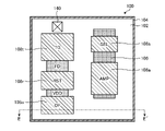
- FIG. 11 is a schematic plan view showing an example of the detailed configuration of the pixel 100 according to the present embodiment, and is a view when the pixel 100 is viewed from above the surface of the semiconductor substrate 102.
- a pixel separation portion 104 made of an insulating film embedded in a groove provided in the semiconductor substrate 102 is provided so as to surround the outer periphery of the pixel 100.
- a photodiode 110 is provided on the semiconductor substrate 102 surrounded by the pixel separation unit 104.
- a gate electrode 108t of the transfer transistor TG and a floating diffusion region FD adjacent to the gate electrode 108t to store electric charges are provided.
- a contact 130 is provided in the upper right corner of the figure of the photodiode 110.
- a reset transistor RST an amplification transistor AMP, and gate electrodes 108r, 108a, 108s of the selection transistor SEL are provided on the semiconductor substrate 102 via an oxide insulating film (not shown). There is.
- planar structure of the pixel 100 according to the present embodiment is not limited to the example shown in FIG. 11, and may include, for example, other elements and the like, and is not particularly limited.
- FIG. 12 is a schematic cross-sectional view showing an example of the detailed configuration of the pixel 100 according to the present embodiment.
- FIG. 12 is a cross-sectional view when the pixel 100 is cut along the line C—C ′ of FIG. 11, and in detail, the lower side in FIG. 12 is the back surface side of the semiconductor substrate 102.
- the upper side of 12 is the front side of the semiconductor substrate 102.
- the n-type semiconductor region 106 is provided in the vicinity of the surface of the semiconductor substrate 102 adjacent to the photodiode 110, and the contact 130 electrically connected to the n-type semiconductor region 106 is provided. ..
- An overflow path for discharging the excess charge generated by the photodiode 110 is formed in the n-type semiconductor region 106 electrically connected to the contact 130, and the excess charge is supplied as a power source through the overflow path. It will be discharged to the circuit.
- the potential of the potential barrier of the overflow path can be adjusted by applying a positive bias via the contact 130. Therefore, the contact 130 is electrically connected to a dedicated power source (a power source capable of generating a positive bias) (adjustment circuit) (not shown) (not shown), which is not shown, and a positive bias is applied.
- a dedicated power source a power source capable of generating a positive bias
- adjustment circuit not shown
- the bias to be applied can be adjusted even when the potential of the potential barrier of the overflow path varies depending on the workmanship of the pixel 100. Therefore, the overflow path can be adjusted.
- the potential of the potential barrier can be controlled to the optimum state.
- the power supply connected to the contact 130 has a simpler configuration than a negative bias power supply that requires a complicated configuration.
- the image pickup device 1 can be miniaturized and the increase in manufacturing cost can be suppressed.
- the cross-sectional structure of the pixel 100 according to the present embodiment is not limited to the example shown in FIG. 12, and may include, for example, other elements and the like, and is not particularly limited.
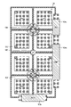
- FIGS. 13 and 14 are schematic plan views showing an example of the detailed configuration of the pixel array unit 30 according to the present embodiment, and are views when the pixels 100 are viewed from above the surface of the semiconductor substrate 102.
- the pixels 100 having the planar structure shown in FIG. 11 may be arranged in a matrix in a 2 ⁇ 2 arrangement. At this time, it is preferable to arrange the pixels 100 so that the floating diffusion region FD is located at the center of the pixel array unit 30. By doing so, each pixel 100 can share one floating diffusion region FD.
- the reset transistor RST, the amplification transistor AMP, and the gate electrodes 108r, 108a, 108s of the selection transistor SEL are provided on the outer periphery of the pixel array unit 30, and each pixel 100 is provided with one each.
- the reset transistor RST, the amplification transistor AMP, and the selection transistor SEL may be shared.
- the pixel array unit 30 in the pixel array unit 30 according to the present embodiment, two configurations shown in FIG. 13 can be arranged, that is, even if the pixels 100 are arranged in a matrix in a 2 ⁇ 4 arrangement. good. Also in the example of FIG. 14, it is preferable to arrange the floating diffusion region FD so as to be located at the center of the four pixels 100, and by doing so, the four pixels 100 share one floating diffusion region FD. can do. Further, in the example shown in FIG. 14, the reset transistor RST, the amplification transistor AMP, and the gate electrodes 108r, 108a, 108s of the selection transistor SEL are provided on the outer periphery of the pixel array unit 30. By doing so, the eight pixels 100 may share one reset transistor RST, an amplification transistor AMP, and a selection transistor SEL.
- planar structure of the pixel array unit 30 according to the present embodiment is not limited to the examples shown in FIGS. 13 and 14, and for example, other numbers of pixels 100 may be arranged, and the plan structure is particularly limited. It's not a thing.
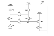
- FIG. 15 is an equivalent circuit diagram of the pixel 100 according to the present embodiment.
- the charge discharge transistor OF may be electrically connected to the capacitor FC instead of the power supply circuit. That is, the excess charge may be discharged to the capacitor FC electrically connected to the overflow path. Further, the capacitor FC may discharge the accumulated charge to the power supply circuit by being controlled by the electrically connected capacitor control transistor FCG. Further, in the present embodiment, the pixel 100 also has a capacitor connection transistor FDG that connects the floating diffusion region FD and the capacitor FC.
- the equivalent circuit of the pixel 100 according to the present embodiment is not limited to the example shown in FIG. 15, and may include, for example, other elements and the like, and is not particularly limited.
- FIG. 16 is a schematic plan view showing an example of the detailed configuration of the pixel 100 according to the present embodiment, and is a view when the pixel 100 is viewed from above the surface of the semiconductor substrate 102.
- a pixel separation unit 104 is provided so as to surround the outer periphery of the pixel 100. Further, on the semiconductor substrate 102 surrounded by the pixel separation unit 104, a charge discharge transistor OF, a transfer transistor TG, a reset transistor RST, an amplification transistor AMP, a selection transistor SEL, and a capacitor control are performed via an insulating film (not shown). The gate electrodes 108o, 108t, 108r, 108a, 108s, 108c, 108d of the transistor FCG and the capacitor connection transistor FDG are provided.
- planar structure of the pixel 100 according to the present embodiment is not limited to the example shown in FIG. 16, and may include, for example, other elements and the like, and is not particularly limited.
- the interface of the region where the overflow path is formed is pinned by the p-type semiconductor region.
- FIG. 17 is a schematic plan view showing an example of the detailed configuration of the pixel 100 according to the present embodiment, and is a view when the pixel 100 is viewed from above the surface of the semiconductor substrate 102.
- the overflow path may be electrically connected to the power supply circuit connected to the reset transistor RST.
- the gate electrodes 108t, 108r, and 108o of the transfer transistor TG, the reset transistor RST, and the charge discharge transistor OF are arranged along the vertical direction in the figure, and the gate electrodes are arranged in a plan view.
- the n-type semiconductor region 106 located between the 108r and the gate electrode 108o is connected to the power supply circuit, and excess charge is discharged through the region.
- planar structure of the pixel 100 according to the present embodiment is not limited to the example shown in FIG. 17, and may include, for example, other elements and the like, and is not particularly limited.
- FIG. 18 is a schematic cross-sectional view showing an example of the detailed configuration of the pixel 100 according to the present embodiment.
- FIG. 18 is a cross-sectional view when the pixel 100 is cut along the line EE of FIG. 17, and in detail, the lower side in FIG. 18 is the back surface side of the semiconductor substrate 102. The upper side of 18 is the surface side of the semiconductor substrate 102.
- the gate electrode (overflow gate) 108o of the charge discharge transistor OF has a flat plate type gate electrode structure.
- the interface in contact with the insulating film 114 or the like has a simple structure, so that the charge is captured at the interface. The phenomenon is less likely to occur, and the generation of dark current can be suppressed.
- the vertical gate electrode structure is not formed, the number of steps is small and the increase in manufacturing cost can be suppressed.
- the cross-sectional structure of the pixel 100 according to the present embodiment is not limited to the example shown in FIG. 18, and may include, for example, other elements and the like, and is not particularly limited.
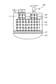
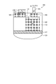
- FIG. 19 is a schematic diagram for explaining the manufacturing method of the pixel 100 according to the present embodiment, and corresponds to the cross section of the pixel 100 at each stage in the manufacturing method.
- a part of the semiconductor substrate 102 is covered with a resist mask, and ions are implanted into a predetermined region in the semiconductor substrate 102 to form the photodiode 110.
- a p-type impurity is ion-implanted into a predetermined region of the semiconductor substrate 102 using a resist mask to form the p-type separation layer 150.
- an n-type impurity is ion-implanted using a resist mask to form an n-type semiconductor region 106.
- a gate electrode 108 having a vertical gate structure is formed.
- the pixel 100 according to the embodiment of the present disclosure can be easily manufactured by using the manufacturing process of the existing semiconductor device.
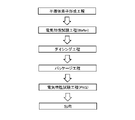
- the image pickup apparatus according to the embodiment of the present disclosure is shipped as a product through a plurality of steps shown in FIG. 20, which is a schematic diagram for explaining the shipping process of the image pickup apparatus 1 according to the present embodiment.
- the electrical characteristics are tested in the form of the wafer (electrical characteristic test step). Wafers judged to be non-defective in the electrical property test process will be sent to the next process.
- the electrical characteristics are tested again in the form of a package (electrical property test step). Then, the image pickup device 1 determined to be a non-defective product will be shipped.
- the pixels 100 are saturated in advance before shipment.
- the signal amount is measured, and the bias applied to the overflow path is adjusted based on the measurement result.
- the image pickup device 1 enclosed in each wafer, each chip, or in the package in the electrical property test step in the form of the package.
- the saturation signal amount is measured by irradiating the image pickup device 1 light for each lot or each lot.
- the value of the bias to be applied is determined based on the measured saturation signal amount with reference to the calibration curve showing the relationship between the saturation signal amount and the bias obtained in advance. Then, in the present embodiment, the determined bias value is stored in the image pickup apparatus 1, and the bias applied to the overflow path by the adjustment circuit is adjusted according to the stored value.
- FIGS. 21 to 23 are block diagrams showing an example of a circuit block according to the present embodiment.
- FIG. 22 is an equivalent circuit diagram showing an example of the fuse cut circuit 52 according to the present embodiment.
- the image pickup apparatus 1 has a circuit block as shown in FIG. 21 to hold a bias determined based on the measured saturation signal amount, and the held bias applies a bias to the overflow path.
- the image pickup apparatus 1 can have a bias setting information holding unit 50 and a fuse cut circuit 52.
- the bias setting information holding unit 50 has an OTP (One Time Program) circuit and can store the determined bias value.
- the fuse cut circuit 52 is a circuit composed of a resistor and a switch, and by selecting a combination of resistors to be used according to the determined bias value, each pixel 100 ( The bias applied to the overflow path of the pixel array unit 30) can be adjusted.
- the image pickup apparatus 1 has a circuit block as shown in FIG. 23 to hold a bias determined based on the measured saturation signal amount, and the held bias applies a bias to the overflow path. May be adjusted.
- the image pickup apparatus 1 may have a logic gate circuit 54 instead of the fuse cut circuit 52.
- the logic gate circuit 54 has a built-in logic circuit, and a bias applied to the overflow path of each pixel 100 (pixel array unit 30) by outputting a predetermined signal from the logic circuit according to the determined bias value. Can be adjusted.
- an overflow path is provided on the photodiode PD independently of the gate electrode 108t of the transfer transistor TR, and a bias applied to the overflow path is further applied by the adjustment circuit. It can be applied to individually adjust the potential of the potential barrier of the overflow path. Further, in each embodiment of the present disclosure, the saturation signal amount is measured in advance for each image pickup device 1, wafer, or lot, and the bias value to be applied is determined based on the measurement result, thereby overflowing. The bias applied to the overflow path can be determined in consideration of the variation in the potential of the potential barrier of the path.
- the variation in the potential of the potential barrier of the overflow path reduces the amount of saturation signal or makes it difficult for excess charge to be discharged, resulting in a decrease in yield. Can be avoided.
- it is possible to improve other characteristics of the pixel 100 by providing an overflow path on the photodiode, independent of the gate of the transfer transistor.
- the pixel 100 in which the first conductive type is n-type, the second conductive type is p-type, and electrons are used as signal charges has been described.
- the morphology is not limited to such examples.
- this embodiment can be applied to a pixel 100 in which the first conductive type is a p-type, the second conductive type is an n-type, and holes are used as signal charges.
- the semiconductor substrate 102 does not necessarily have to be a silicon substrate, but may be another substrate (for example, an SOI (Silicon On Insulator) substrate, a SiGe substrate, or the like). Further, the semiconductor substrate 102 may have a semiconductor structure or the like formed on such various substrates.
- SOI Silicon On Insulator
- the image pickup device 1 is not limited to the image pickup device that detects the distribution of the incident light amount of visible light and captures the image as an image.
- an image pickup device that captures the distribution of incident amounts of infrared rays, X-rays, particles, etc. as an image, and a fingerprint that detects the distribution of other physical quantities such as pressure and capacitance and captures images as an image. It can be applied to an image pickup device (physical quantity distribution detection device) such as a detection sensor.
- the image pickup apparatus 1 according to the embodiment of the present disclosure can be manufactured by using the methods, devices, and conditions used for manufacturing a general semiconductor device. That is, the image pickup apparatus 1 according to the present embodiment can be manufactured by using the manufacturing process of the existing semiconductor device.
- Examples of the above-mentioned manufacturing method include a PVD (Physical Vapor Deposition) method, a CVD (Chemical Vapor Deposition) method, and an ALD (Atomic Layer Deposition) method.
- the PVD method includes a vacuum vapor deposition method, an EB (electron beam) vapor deposition method, various sputtering methods (magnetron sputtering method, RF (Radio Frequency) -DC (Direct Current) combined bias sputtering method, and ECR (Electron Cyclotron Precision) sputtering method.
- examples of the CVD method include a plasma CVD method, a thermal CVD method, an organic metal (MO) CVD method, and an optical CVD method.
- Various printing methods such as method and flexographic printing method; stamp method; spray method; air doctor coater method, blade coater method, rod coater method, knife coater method, squeeze coater method, reverse roll coater method, transfer roll coater method, gravure coater method.
- Kiss coater method, cast coater method, spray coater method, slit orifice coater method, calendar coater method and various other coating methods can be mentioned.
- examples of the patterning method include shadow mask, laser transfer, chemical etching such as photolithography, and physical etching by ultraviolet rays or laser.
- examples of the flattening technique include a CMP (Chemical Mechanical Polishing) method, a laser flattening method, a reflow method, and the like.
- each step in the manufacturing method according to the embodiment of the present disclosure described above does not necessarily have to be processed in the order described.
- each step may be processed in an appropriately reordered manner.
- the method used in each step does not necessarily have to be performed according to the described method, and may be performed by another method.
- the technique according to the present disclosure can be further applied to various products.
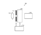
- the technique according to the present disclosure may be applied to a camera or the like. Therefore, with reference to FIG. 24, a configuration example of the camera 700 as an electronic device to which the present technology is applied will be described.
- FIG. 24 is an explanatory diagram showing an example of a schematic functional configuration of the camera 700 to which the technique according to the present disclosure (the present technique) can be applied.
- the camera 700 includes an image pickup device 702, an optical lens 710, a shutter mechanism 712, a drive circuit unit 714, and a signal processing circuit unit 716.
- the optical lens 710 forms an image of image light (incident light) from the subject on the image pickup surface of the image pickup apparatus 702.
- the signal charge is accumulated in the pixel 100 of the image pickup apparatus 702 for a certain period of time.
- the shutter mechanism 712 controls the light irradiation period and the light shielding period to the image pickup apparatus 702 by opening and closing.
- the drive circuit unit 714 supplies drive signals for controlling the signal transfer operation of the image pickup apparatus 702, the shutter operation of the shutter mechanism 712, and the like.
- the image pickup apparatus 702 performs signal transfer based on the drive signal (timing signal) supplied from the drive circuit unit 714.
- the signal processing circuit unit 716 performs various signal processing. For example, the signal processing circuit unit 716 outputs the signal-processed video signal to a storage medium (not shown) such as a memory, or outputs it to a display unit (not shown).
- FIG. 25 is a block diagram showing an example of a schematic functional configuration of a smartphone 900 to which the technique according to the present disclosure (the present technique) can be applied.
- the smartphone 900 includes a CPU (Central Processing Unit) 901, a ROM (Read Only Memory) 902, and a RAM (Random Access Memory) 903.
- the smartphone 900 also includes a storage device 904, a communication module 905, and a sensor module 907.
- the smartphone 900 includes an image pickup device 909, a display device 910, a speaker 911, a microphone 912, an input device 913, and a bus 914.
- the smartphone 900 may have a processing circuit such as a DSP (Digital Signal Processor) in place of or in combination with the CPU 901.
- DSP Digital Signal Processor
- the CPU 901 functions as an arithmetic processing device and a control device, and controls all or a part of the operation in the smartphone 900 according to various programs recorded in the ROM 902, the RAM 903, the storage device 904, and the like.
- the ROM 902 stores programs, calculation parameters, and the like used by the CPU 901.
- the RAM 903 primary stores a program used in the execution of the CPU 901, parameters that appropriately change in the execution, and the like.
- the CPU 901, ROM 902, and RAM 903 are connected to each other by a bus 914.
- the storage device 904 is a data storage device configured as an example of the storage unit of the smartphone 900.
- the storage device 904 is composed of, for example, a magnetic storage device such as an HDD (Hard Disk Drive), a semiconductor storage device, an optical storage device, and the like.
- the storage device 904 stores programs executed by the CPU 901, various data, various data acquired from the outside, and the like.
- the communication module 905 is a communication interface composed of, for example, a communication device for connecting to the communication network 906.
- the communication module 905 may be, for example, a communication card for a wired or wireless LAN (Local Area Network), Bluetooth (registered trademark), WUSB (Wireless USB), or the like. Further, the communication module 905 may be a router for optical communication, a router for ADSL (Asymmetric Digital Subscriber Line), a modem for various communications, or the like.
- the communication module 905 transmits and receives signals and the like to and from the Internet and other communication devices using a predetermined protocol such as TCP (Transmission Control Protocol) / IP (Internet Protocol).
- the communication network 906 connected to the communication module 905 is a network connected by wire or wirelessly, and is, for example, the Internet, a home LAN, infrared communication, satellite communication, or the like.
- the sensor module 907 is, for example, a motion sensor (for example, an acceleration sensor, a gyro sensor, a geomagnetic sensor, etc.), a biometric information sensor (for example, a pulse sensor, a blood pressure sensor, a fingerprint sensor, etc.), or a position sensor (for example, GNSS (Global Navigation)). Includes various sensors such as Satellite System) receivers, etc.).
- a motion sensor for example, an acceleration sensor, a gyro sensor, a geomagnetic sensor, etc.
- a biometric information sensor for example, a pulse sensor, a blood pressure sensor, a fingerprint sensor, etc.
- GNSS Global Navigation
- the image pickup device 909 is provided on the surface of the smartphone 900 and can image an object or the like located on the back side or the front side of the smartphone 900.
- the image pickup device 909 is for an image pickup element (not shown) such as a CMOS (Complementary MOS) image sensor to which the technique (the present technique) according to the present disclosure can be applied, and a signal photoelectrically converted by the image pickup element. It can be configured to include a signal processing circuit (not shown) that performs image pickup signal processing.
- the image pickup apparatus 909 further includes an optical system mechanism (not shown) composed of an image pickup lens, a zoom lens, a focus lens, and the like, and a drive system mechanism (not shown) that controls the operation of the optical system mechanism.
- the image pickup element collects the incident light from the object as an optical image
- the signal processing circuit photoelectrically converts the imaged optical image on a pixel-by-pixel basis and reads out the signal of each pixel as an image pickup signal.
- the captured image can be acquired by image processing.
- the display device 910 is provided on the surface of the smartphone 900, and can be, for example, a display device such as an LCD (Liquid Crystal Display) or an organic EL (Electro Luminescence) display.
- the display device 910 can display an operation screen, an image captured by the image pickup device 909 described above, and the like.
- the speaker 911 can output, for example, call voice, voice accompanying the video content displayed by the above-mentioned display device 910, and the like to the user.
- the microphone 912 can collect, for example, a user's call voice, a voice including a command for activating a function of the smartphone 900, and a voice of the surrounding environment of the smartphone 900.
- the input device 913 is a device operated by the user, such as a button, a keyboard, a touch panel, and a mouse.
- the input device 913 includes an input control circuit that generates an input signal based on the information input by the user and outputs the input signal to the CPU 901.
- the user can input various data to the smartphone 900 and instruct the processing operation.
- the configuration example of the smartphone 900 is shown above.
- Each of the above components may be configured by using general-purpose members, or may be configured by hardware specialized for the function of each component. Such a configuration may be changed as appropriate depending on the technical level at the time of implementation.
- the present technology can also have the following configurations.
- a photoelectric conversion unit that converts light into electric charges
- An overflow path that discharges the excess charge and An adjustment circuit that adjusts the potential barrier of the overflow path
- a solid-state image sensor Provided on the semiconductor substrate, A photoelectric conversion unit that converts light into electric charges, A charge storage unit to which the charge is transferred from the photoelectric conversion unit and a charge storage unit An overflow path that discharges the excess charge and An adjustment circuit that adjusts the potential barrier of the overflow path, and A solid-state image sensor.
- the overflow gate has a vertical gate electrode structure having an embedded portion embedded in the semiconductor substrate.
- the solid-state image pickup device according to any one of (1) to (8) above, wherein the overflow path is electrically connected to a power supply circuit.
- the solid-state image sensor according to any one of (1) to (8) above, wherein the overflow path is electrically connected to a capacitor.
- the adjustment circuit adjusts the potential barrier based on the measurement result of the saturation signal amount of the photoelectric conversion unit.
- the adjustment circuit includes a fuse cut circuit.
- the adjustment circuit includes a logic gate circuit.
- a photoelectric conversion unit that converts light into electric charges
- An overflow path that discharges the excess charge
- An adjustment circuit that adjusts the potential barrier of the overflow path, and It is a method of adjusting the potential barrier of the solid-state image sensor having the above.
- the adjustment circuit adjusts the potential barrier based on the measurement result of the saturation signal amount of the photoelectric conversion unit. Adjustment method including that.
- a photoelectric conversion unit that converts light into electric charges
- An overflow path that discharges the excess charge and An adjustment circuit that adjusts the potential barrier of the overflow path
- An electronic device equipped with a solid-state image sensor provided on the semiconductor substrate.
- 1,702,909 Imaging device 10 102 Semiconductor board 30 Pixel array part 32 Vertical drive circuit part 34 Column signal processing circuit part 36 Horizontal drive circuit part 38 Output circuit part 40 Control circuit part 42 Pixel drive wiring 44 Vertical signal line 46 Horizontal Signal line 48 Input / output terminal 50 Bias setting information holding part 52 Fuse cut circuit 54 Logic gate circuit 100 pixels 104 Pixel separation part 106 n-type semiconductor area 108 Gate electrode 110 photodiode 114 Insulation film 116 p-type semiconductor area 118 Embedded part 120 on Chip lens 122 Antireflection film 130, 140 Contact 150 p-type separation layer 700 Camera 710 Optical lens 712 Shutter mechanism 714 Drive circuit unit 716 Signal processing circuit unit 900 Smartphone 901 CPU 902 ROM 903 RAM 904 Storage device 905 Communication module 906 Communication network 907 Sensor module 910 Display device 911 Speaker 912 Microphone 913 Input device 914 Bus
Landscapes
- Engineering & Computer Science (AREA)
- Multimedia (AREA)
- Signal Processing (AREA)
- Solid State Image Pick-Up Elements (AREA)
- Metal-Oxide And Bipolar Metal-Oxide Semiconductor Integrated Circuits (AREA)
- Design And Manufacture Of Integrated Circuits (AREA)
- Light Receiving Elements (AREA)
- Transforming Light Signals Into Electric Signals (AREA)
- Semiconductor Integrated Circuits (AREA)
Abstract
半導体基板(102)に設けられた、光を電荷に変換する光電変換部(110)と、前記光電変換部から前記電荷が転送される電荷蓄積部(FD)と、余剰の前記電荷を排出するオーバーフローパスと、前記オーバーフローパスの電位障壁を調整する調整回路と、を備える、固体撮像装置(100)を提供する。
Description
本開示は、固体撮像装置、調整方法及び電子機器に関する。
被写体の撮影を行う撮像装置には、画素として、MOS(Metal-Oxide-Semiconductor)集積回路と同様のプロセスで製造することができるCMOS(Complementary MOS)型固体撮像素子を適用することができる。固体撮像素子は、CMOSプロセスに付随した微細化技術により、画素毎に増幅機能を持つアクティブ型の構造を容易に作ることができるという特徴を有する。さらに、固体撮像素子は、画素の集合体である画素アレイ部を駆動する駆動回路や画素アレイ部の各画素から出力される信号を処理する信号処理回路などの周辺回路部を、画素アレイ部と同一の半導体基板(チップ)上に集積できるという特徴を有する。このような特徴から、CMOS型固体撮像素子の開発が盛んになされている。
従来から、上述の固体撮像素子に対して多量の光が照射された際に、固体撮像素子の有するフォトダイオードから溢れ出た余剰の電荷をどのように取り扱うかについて検討がなされており、余剰の電荷を排出するための様々な構造が提案されている。例えば、余剰の電荷をフォトダイオードからオーバーフローさせることができる様々な構造が提案されているが、飽和信号量(閾値)を超えた場合にオーバーフローさせるとした場合に、飽和信号量を定めるオーバーフロー電位障壁のポテンシャルを精度よく制御することは難しい。従って、いずれの構造においても、オーバーフロー電位障壁のポテンシャルのばらつきが発生することを避けることが難しく、飽和信号量の低下や、歩留まりの低下を招くこととなる。
そこで、本開示では、飽和信号量の低下や、歩留まりの低下を避けることができる、固体撮像装置、調整方法及び電子機器を提案する。
本開示によれば、半導体基板に設けられた、光を電荷に変換する光電変換部と、前記光電変換部から前記電荷が転送される電荷蓄積部と、余剰の前記電荷を排出するオーバーフローパスと、前記オーバーフローパスの電位障壁を調整する調整回路と、を備える、固体撮像装置が提供される。
また、本開示によれば、半導体基板に設けられた、光を電荷に変換する光電変換部と、前記光電変換部から前記電荷が転送される電荷蓄積部と、余剰の前記電荷を排出するオーバーフローパスと、前記オーバーフローパスの電位障壁を調整する調整回路と、を有する固体撮像装置の前記電位障壁の調整方法であって、前記調整回路は、光電変換部の飽和信号量の測定結果に基づき、前記電位障壁を調整する、ことを含む、調整方法が提供される。
さらに、本開示によれば、半導体基板に設けられた、光を電荷に変換する光電変換部と、前記光電変換部から前記電荷が転送される電荷蓄積部と、余剰の前記電荷を排出するオーバーフローパスと、前記オーバーフローパスの電位障壁を調整する調整回路と、を有する固体撮像装置を、搭載する電子機器が提供される。
以下に、本開示の実施形態について図面に基づいて詳細に説明する。なお、以下の各実施形態において、同一の部位には同一の符号を付することにより重複する説明を省略する。
また、本明細書および図面において、実質的に同一または類似の機能構成を有する複数の構成要素を、同一の符号の後に異なる数字を付して区別する場合がある。ただし、実質的に同一または類似の機能構成を有する複数の構成要素の各々を特に区別する必要がない場合、同一符号のみを付する。また、異なる実施形態の類似する構成要素については、同一の符号の後に異なるアルファベットを付して区別する場合がある。ただし、類似する構成要素の各々を特に区別する必要がない場合、同一符号のみを付する。
また、以下の説明で参照される図面は、本開示の一実施形態の説明とその理解を促すための図面であり、わかりやすくするために、図中に示される形状や寸法、比などは実際と異なる場合がある。さらに、図中に示される撮像装置は、以下の説明と公知の技術を参酌して適宜、設計変更することができる。また、撮像装置の断面図を用いた説明においては、撮像装置の積層構造の上下方向は、撮像装置に対して入射する光が入ってくる受光面を下とした場合の相対方向に対応し、実際の重力加速度に従った上下方向とは異なる場合がある。
さらに、以下の説明においては、本開示の実施形態を裏面照射型撮像装置に適用した場合を例に説明し、従って、当該撮像装置においては、基板の裏面側から光が入射されることとなる。従って、以下の説明においては、基板の表面とは、光が入射される側を裏面とした場合に、裏面と対向する表面となる。
また、以下の回路(電気的な接続)の説明においては、特段の断りがない限りは、「電気的に接続」とは、複数の要素の間を電気(信号)が導通するように接続することを意味する。加えて、以下の説明における「電気的に接続」には、複数の要素を直接的に、且つ、電気的に接続する場合だけでなく、他の要素を介して間接的に、且つ、電気的に接続する場合も含むものとする。
以下、本開示を実施するための形態について、図面を参照して詳細に説明する。なお、説明は以下の順序で行う。
1. 撮像装置の概略構成
2. 本発明者が本開示に係る実施形態を創作するに至った背景
3. 第1の実施形態
3.1 等価回路
3.2 平面構造
3.3 断面構造
4. 第2の実施形態
5. 第3の実施形態
6. 第4の実施形態
7. 第5の実施形態
7.1 平面構造
7.2 断面構造
8. 第6の実施形態
9. 第7の実施形態
9.1 平面構造
9.2 断面構造
9.3 画素アレイ部30の平面構造
10. 第8の実施形態
10.1 等価回路
10.2 平面構造
11. 第9の実施形態
11.1 平面構造
11.2 断面構造
12. 第10の実施形態
13. 第11の実施形態
14.まとめ
15. カメラへの応用例
16. スマートフォンへの応用例
17. 補足
1. 撮像装置の概略構成
2. 本発明者が本開示に係る実施形態を創作するに至った背景
3. 第1の実施形態
3.1 等価回路
3.2 平面構造
3.3 断面構造
4. 第2の実施形態
5. 第3の実施形態
6. 第4の実施形態
7. 第5の実施形態
7.1 平面構造
7.2 断面構造
8. 第6の実施形態
9. 第7の実施形態
9.1 平面構造
9.2 断面構造
9.3 画素アレイ部30の平面構造
10. 第8の実施形態
10.1 等価回路
10.2 平面構造
11. 第9の実施形態
11.1 平面構造
11.2 断面構造
12. 第10の実施形態
13. 第11の実施形態
14.まとめ
15. カメラへの応用例
16. スマートフォンへの応用例
17. 補足
<<1.撮像装置の概略構成>>
まずは、図1を参照して、本開示の実施形態に係る撮像装置1の概略構成について説明する。図1は、本開示の実施形態に係る撮像装置1の平面構成例を示す説明図である。図1に示すように、本開示の実施形態に係る撮像装置1は、例えば、シリコンからなる半導体基板10上に、複数の画素100がマトリック状に配置されている画素アレイ部30と、当該画素アレイ部30を取り囲むように設けられた周辺回路部とを有する。さらに、上記撮像装置1には、当該周辺回路部として、垂直駆動回路部32、カラム信号処理回路部34、水平駆動回路部36、出力回路部38、制御回路部40等が含まれる。以下に、撮像装置1の各ブロックの詳細について説明する。
まずは、図1を参照して、本開示の実施形態に係る撮像装置1の概略構成について説明する。図1は、本開示の実施形態に係る撮像装置1の平面構成例を示す説明図である。図1に示すように、本開示の実施形態に係る撮像装置1は、例えば、シリコンからなる半導体基板10上に、複数の画素100がマトリック状に配置されている画素アレイ部30と、当該画素アレイ部30を取り囲むように設けられた周辺回路部とを有する。さらに、上記撮像装置1には、当該周辺回路部として、垂直駆動回路部32、カラム信号処理回路部34、水平駆動回路部36、出力回路部38、制御回路部40等が含まれる。以下に、撮像装置1の各ブロックの詳細について説明する。
(画素アレイ部30)
画素アレイ部30は、半導体基板10上に、行方向及び列方向に沿ってマトリックス状に、2次元配置された複数の画素100を有する。各画素100は、入射された光に対して光電変換を行い、電荷を発生させるフォトダイオード(光電変換部)(図示省略)と、複数の画素トランジスタ(例えばMOS(Metal-Oxide-Semiconductor)トランジスタ)(図示省略)とを有している。そして、当該画素トランジスタは、例えば、転送トランジスタ、選択トランジスタ、リセットトランジスタ、及び、増幅トランジスタの4つのMOSトランジスタを含む。さらに、画素アレイ部30においては、例えばベイヤー配列に従って、複数の画素100が2次元状に配列している。ここで、ベイヤー配列とは、緑色の波長(例えば波長495nm~570nm)をもつ光を吸収して電荷を発生する画素100が市松状に並び、残りの部分に、赤色の波長(例えば波長620nm~750nm)をもつ光を吸収して電荷を発生する画素100と、青色の波長(例えば波長450nm~495nm)をもつ光を吸収して電荷を発生する画素100とが一列ごとに交互に並ぶような、配列パターンである。なお、画素100の詳細構造については後述する。
画素アレイ部30は、半導体基板10上に、行方向及び列方向に沿ってマトリックス状に、2次元配置された複数の画素100を有する。各画素100は、入射された光に対して光電変換を行い、電荷を発生させるフォトダイオード(光電変換部)(図示省略)と、複数の画素トランジスタ(例えばMOS(Metal-Oxide-Semiconductor)トランジスタ)(図示省略)とを有している。そして、当該画素トランジスタは、例えば、転送トランジスタ、選択トランジスタ、リセットトランジスタ、及び、増幅トランジスタの4つのMOSトランジスタを含む。さらに、画素アレイ部30においては、例えばベイヤー配列に従って、複数の画素100が2次元状に配列している。ここで、ベイヤー配列とは、緑色の波長(例えば波長495nm~570nm)をもつ光を吸収して電荷を発生する画素100が市松状に並び、残りの部分に、赤色の波長(例えば波長620nm~750nm)をもつ光を吸収して電荷を発生する画素100と、青色の波長(例えば波長450nm~495nm)をもつ光を吸収して電荷を発生する画素100とが一列ごとに交互に並ぶような、配列パターンである。なお、画素100の詳細構造については後述する。
(垂直駆動回路部32)
垂直駆動回路部32は、例えばシフトレジスタによって形成され、画素駆動配線42を選択し、選択された画素駆動配線42に画素100を駆動するためのパルスを供給し、行単位で画素100を駆動する。すなわち、垂直駆動回路部32は、画素アレイ部30の各画素100を行単位で順次垂直方向(図1中の上下方向)に選択走査し、各画素100の光電変換部(図示省略)の受光量に応じて生成された信号電荷に基づく画素信号を、垂直信号線44を通して後述するカラム信号処理回路部34に供給する。
垂直駆動回路部32は、例えばシフトレジスタによって形成され、画素駆動配線42を選択し、選択された画素駆動配線42に画素100を駆動するためのパルスを供給し、行単位で画素100を駆動する。すなわち、垂直駆動回路部32は、画素アレイ部30の各画素100を行単位で順次垂直方向(図1中の上下方向)に選択走査し、各画素100の光電変換部(図示省略)の受光量に応じて生成された信号電荷に基づく画素信号を、垂直信号線44を通して後述するカラム信号処理回路部34に供給する。
(カラム信号処理回路部34)
カラム信号処理回路部34は、画素100の列ごとに配置されており、1行分の画素100から出力される画素信号に対して画素列ごとにノイズ除去等の信号処理を行う。例えば、カラム信号処理回路部34は、画素固有の固定パターンノイズを除去するためにCDS(Correlated Double Sampling:相関2重サンプリング)およびAD(Analog-Degital)変換等の信号処理を行う。
カラム信号処理回路部34は、画素100の列ごとに配置されており、1行分の画素100から出力される画素信号に対して画素列ごとにノイズ除去等の信号処理を行う。例えば、カラム信号処理回路部34は、画素固有の固定パターンノイズを除去するためにCDS(Correlated Double Sampling:相関2重サンプリング)およびAD(Analog-Degital)変換等の信号処理を行う。
(水平駆動回路部36)
水平駆動回路部36は、例えばシフトレジスタによって形成され、水平走査パルスを順次出力することによって、上述したカラム信号処理回路部34の各々を順番に選択し、カラム信号処理回路部34の各々から画素信号を水平信号線46に出力させる。
水平駆動回路部36は、例えばシフトレジスタによって形成され、水平走査パルスを順次出力することによって、上述したカラム信号処理回路部34の各々を順番に選択し、カラム信号処理回路部34の各々から画素信号を水平信号線46に出力させる。
(出力回路部38)
出力回路部38は、上述したカラム信号処理回路部34の各々から水平信号線46を通して順次に供給される画素信号に対し、信号処理を行って出力する。出力回路部38は、例えば、バッファリング(buffering)を行う機能部として機能してもよく、もしくは、黒レベル調整、列ばらつき補正、各種デジタル信号処理等の処理を行ってもよい。なお、バッファリングとは、画素信号のやり取りの際に、処理速度や転送速度の差を補うために、一時的に画素信号を保存することをいう。さらに、入出力端子48は、外部装置との間で信号のやり取りを行うための端子である。
出力回路部38は、上述したカラム信号処理回路部34の各々から水平信号線46を通して順次に供給される画素信号に対し、信号処理を行って出力する。出力回路部38は、例えば、バッファリング(buffering)を行う機能部として機能してもよく、もしくは、黒レベル調整、列ばらつき補正、各種デジタル信号処理等の処理を行ってもよい。なお、バッファリングとは、画素信号のやり取りの際に、処理速度や転送速度の差を補うために、一時的に画素信号を保存することをいう。さらに、入出力端子48は、外部装置との間で信号のやり取りを行うための端子である。
(制御回路部40)
制御回路部40は、入力クロックと、動作モード等を指令するデータを受け取り、また撮像装置1の内部情報等のデータを出力する。すなわち、制御回路部40は、垂直同期信号、水平同期信号及びマスタクロックに基づいて、垂直駆動回路部32、カラム信号処理回路部34及び水平駆動回路部36等の動作の基準となるクロック信号や制御信号を生成する。そして、制御回路部40は、生成したクロック信号や制御信号を、垂直駆動回路部32、カラム信号処理回路部34及び水平駆動回路部36等に出力する。
制御回路部40は、入力クロックと、動作モード等を指令するデータを受け取り、また撮像装置1の内部情報等のデータを出力する。すなわち、制御回路部40は、垂直同期信号、水平同期信号及びマスタクロックに基づいて、垂直駆動回路部32、カラム信号処理回路部34及び水平駆動回路部36等の動作の基準となるクロック信号や制御信号を生成する。そして、制御回路部40は、生成したクロック信号や制御信号を、垂直駆動回路部32、カラム信号処理回路部34及び水平駆動回路部36等に出力する。
<<2. 本発明者が本開示に係る実施形態を創作するに至った背景>>
次に、本開示に係る実施形態の詳細を説明する前に、本発明者が本開示に係る実施形態を創作するに至った背景について説明する。
次に、本開示に係る実施形態の詳細を説明する前に、本発明者が本開示に係る実施形態を創作するに至った背景について説明する。
先に説明したように、撮像装置1には、画素100として、MOS集積回路と同様のプロセスで製造できるCMOS型固体撮像素子を適用することができる。固体撮像素子は、CMOSプロセスに付随した微細化技術により、画素100毎に増幅機能を持つアクティブ型の構造を容易に作ることができるという特徴を有する。さらに、固体撮像素子は、画素アレイ部30を駆動する駆動回路や画素アレイ部30の各画素100から出力される信号を処理する信号処理回路などの周辺回路部を、画素アレイ部30と同一の半導体基板(チップ)10上に集積できるという特徴を有する。このような特徴から、CMOS型固体撮像素子の開発が盛んになされている。
このような固体撮像素子のうち、半導体基板10の裏面の光が照射される裏面照射型撮像素子がある。従来から、固体撮像素子としての画素100に対して多量の光が照射された際に、フォトダイオードから溢れ出た余剰の電荷をどのように取り扱いかについて検討がなされており、余剰の電荷を排出するための様々な構造が提案されている。余剰の電荷が隣接する画素100へ流れだした場合には、隣接する画素100は、意図しない画素信号を発生することから、本来あるべき像を撮像することができない。このような現象はブルーミングと呼ばれている。
例えば、従来検討された構造としては、フォトダイオードからの電荷を浮遊拡散領域に転送する転送トランジスタのゲート下から、浮遊拡散領域へ余剰の電荷をオーバーフローさせることができる構造が挙げられる。
このような構造を選択した場合、固体撮像素子の製造においては、転送トランジスタのゲート下の領域に形成されるオーバーフローパスの電位障壁のポテンシャルを精度よく所望の状態にしつつ、高速で電荷を転送することができるように、転送トランジスタのゲート下の領域の不純物プロファイルを精度よく制御することが求められる。すなわち、上記構造によれば、オーバーフローパスの電位障壁のポテンシャル制御と転送設計との2つを同時に満たさなくてはならないことから、製造(量産)の難易度が高くなる。そして、転送トランジスタのゲート下の領域の不純物プロファイルを精度よく制御して製造することが難しいことから、オーバーフローパスの電位障壁のポテンシャルはばらつき、画素によっては、飽和信号量が低下したり、もしくは、余剰の電荷が排出され難くなり、歩留まりの低下を招くこととなる。加えて、上記構造によれば、オーバーフローパスの電位障壁のポテンシャル制御を優先することにより、画素100の他の特性が劣化する場合もある。
また、他の構造としては、例えば、浮遊拡散領域の下に、半導体基板10の膜厚方向に余剰電荷を輩出するためのオーバーフローパスを形成することにより、転送設計とは独立して、オーバーフローパスの電位障壁のポテンシャルを制御することが可能な構造を挙げることができる。当該構造においては、オーバーフローパスを設けるために、例えば、半導体基板10の膜厚方向に沿って、n型半導体領域-p型半導体領域-n型半導体領域を形成する。しかしながら、当該構造においても、オーバーフローパスが設けられる領域の不純物プロファイルを精度よく制御することが難しく、オーバーフローパスの電位障壁のポテンシャルのばらつきが発生することを避けることが難しい。そのため、当該構造においても、飽和信号量の低下や、歩留まりの低下を招くこととなる。
そこで、上述のような状況を鑑みて、本発明者は、転送トランジスタのゲートと独立して、フォトダイオードの上にオーバーフローパスを設け、さらに、オーバーフローパスの電位障壁のポテンシャルを印加するバイアスにより個別に調整することができるような画素100の構造を創作するに至った。さらに、本発明者が創作した本開示の実施形態においては、撮像装置1ごと、ウエハーごと、もしくは、ロットごとに飽和信号量を予め計測し、計測結果に基づいて、印加するバイアスの値を決定することにより、オーバーフローパスの電位障壁のポテンシャルのばらつきを加味した上で、オーバーフローパスに印加するバイアスを決定することができる。このような本発明者が創作した本開示の実施形態においては、オーバーフローパスの電位障壁のポテンシャルのばらつきにより、飽和信号量が低下したり、もしくは、余剰の電荷が排出され難くなり、歩留まりの低下を招くことを避けることができる。加えて、上記構造によれば、転送トランジスタのゲートと独立して、フォトダイオードの上にオーバーフローパスを設けることから、画素100の他の特性を向上させることも可能となる。以下に、本発明者が創作した本開示の実施形態の詳細について順次説明する。
<<3. 第1の実施形態>>
<3.1 等価回路>
まずは、図2を参照して、本発明者が創作した本開示の第1の実施形態に係る画素100の等価回路を説明する。図2は、本実施形態に係る画素100の等価回路図である。
<3.1 等価回路>
まずは、図2を参照して、本発明者が創作した本開示の第1の実施形態に係る画素100の等価回路を説明する。図2は、本実施形態に係る画素100の等価回路図である。
図2に示すように、画素100は、光を電荷に変換する光電変換素子(光電変換部)としてのフォトダイオードPDと、電荷排出トランジスタOFとを有する。さらに、画素100は、転送トランジスタTG、浮遊拡散領域FD、リセットトランジスタRST、増幅トランジスタAMP、及び選択トランジスタSELを有する。
詳細には、図2に示すように、画素100においては、電荷排出トランジスタOFのソース/ドレインの一方は、受光することで電荷を発生するフォトダイオードPDに電気的に接続される。さらに、電荷排出トランジスタOFのソース/ドレインの他方は、電源回路(電源電位VDD)に電気的に接続される。そして、電荷排出トランジスタOFは、自身のゲートに印加された電圧に応じて、フォトダイオードPDからの余剰の電荷を上記電源回路(電源電位VDD)に排出することができる。
また、図2に示すように、画素100においては、転送トランジスタTGのソース/ドレインの一方は、フォトダイオードPDに電気的に接続され、転送トランジスタTGのソース/ドレインの他方は、浮遊拡散領域FDに電気的に接続される。そして、転送トランジスタTGは、自身のゲートに印加された電圧に応じて導通状態になり、フォトダイオードPDで発生した電荷を浮遊拡散領域FDに転送することができる。
また、浮遊拡散領域FDは、電荷を電圧に変換して信号として出力する増幅トランジスタAMPのゲートに電気的に接続される。また、増幅トランジスタAMPのソース/ドレインの一方は、選択信号に従って、変換によって得た上記信号を信号線に出力する選択トランジスタのソース/ドレインの一方に電気的に接続される。さらに、増幅トランジスタAMPのソース/ドレインの他方は、電源回路(電源電位VDD)に電気的に接続される。
また、選択トランジスタSELのソース/ドレインの他方は、変換された電圧を信号として伝達する上記信号線に電気的に接続され、さらに上述したカラム信号処理回路部34に電気的に接続される。さらに、選択トランジスタSELのゲートは、信号を出力する行を選択する選択線(図示省略)に電気的に接続され、さらに上述した垂直駆動回路部32に電気的に接続される。すなわち、浮遊拡散領域FDに蓄積された電荷は、選択トランジスタSELの制御により、増幅トランジスタAMP2によって電圧に変換され、信号線に出力されることとなる。
また、図2に示すように、浮遊拡散領域FDは、蓄積した電荷をリセットするためのリセットトランジスタRSTのドレイン/ソースの一方に電気的に接続される。リセットトランジスタRSTのゲートは、リセット信号線(図示省略)に電気的に接続され、さらに上述した垂直駆動回路部32に電気的に接続される。また、リセットトランジスタRSTのドレイン/ソースの他方は、電源回路(電源電位VDD)に電気的に接続される。そして、リセットトランジスタRSTは、自身のゲートに印加された電圧に応じて導通状態になり、浮遊拡散領域FDに蓄積された電荷をリセット(電源回路(電源電位VDD)へ排出)することができる。
なお、本実施形態に係る画素100の等価回路は、図2に示される例に限定されるものではなく、例えば、他の素子等を含んでもよく、特に限定されるものではない。
<3.2 平面構造>
まずは、図3を参照して、本開示の第1の実施形態に係る画素100の平面構造例を説明する。図3は、本実施形態に係る画素100の詳細構成の一例を表す平面模式図であって、半導体基板102の表面の上方から画素100を見た場合の図となる。
まずは、図3を参照して、本開示の第1の実施形態に係る画素100の平面構造例を説明する。図3は、本実施形態に係る画素100の詳細構成の一例を表す平面模式図であって、半導体基板102の表面の上方から画素100を見た場合の図となる。
図3に示すように、画素100においては、画素100の外周を取り囲むように、半導体基板102に設けられた溝に埋め込まれた絶縁膜からなる画素分離部104が設けられている。また、画素分離部104に取り囲まれたp型(第2の導電型)半導体基板102には、n型(第1の導電型)半導体領域106が設けられている。さらに、半導体基板102上には、酸化絶縁膜(図示省略)を介して、電荷排出トランジスタOF、転送トランジスタTG、リセットトランジスタRST、増幅トランジスタAMP、及び選択トランジスタSELのゲート電極108o、108t、108r、108a、108sが設けられている。
詳細には、図3に示すように、転送トランジスタTG及びリセットトランジスタRSTのゲート電極108t、108rが、図中上下方向に沿って並んでおり、平面視において、ゲート電極108tとゲート電極108rとの間に位置するn型半導体領域が、電荷を蓄積する浮遊拡散領域FDとして機能する。さらに、電荷排出トランジスタOF、増幅トランジスタAMP、及び選択トランジスタSELのゲート電極108o、108a、108sが、図中上下方向に沿って並んでおり、平面視において、これらゲート電極108o、108a、108sに挟まれたn型半導体領域が、これらトランジスタのソース又はドレインとして機能する。また、画素分離部104に取り囲まれたp型半導体基板102には、p型半導体基板のpウェル領域(図示省略)を所定の電位にするためのコンタクト140が設けられる。
なお、本実施形態に係る画素100の平面構造は、図3に示される例に限定されるものではなく、例えば、他の素子等を含んでもよく、特に限定されるものではない。
<3.3 断面構造>
次に、図4を参照して、本開示の第1の実施形態に係る画素100の断面構造例を説明する。図4は、本実施形態に係る画素100の詳細構成の一例を表す断面模式図である。詳細には、図4は、図3のA―A´線に沿って画素100を切断した際の断面図であり、詳細には、図4中の下側が半導体基板102の裏面側となり、図4中の上側が半導体基板102の表面側となる。
次に、図4を参照して、本開示の第1の実施形態に係る画素100の断面構造例を説明する。図4は、本実施形態に係る画素100の詳細構成の一例を表す断面模式図である。詳細には、図4は、図3のA―A´線に沿って画素100を切断した際の断面図であり、詳細には、図4中の下側が半導体基板102の裏面側となり、図4中の上側が半導体基板102の表面側となる。
まずは、図4に示すように、画素100は、シリコン基板等からなる半導体基板102を有する。詳細には、半導体基板102内には、p型半導体領域(図示省略)とn型半導体領域(図示省略)が積層されることにより、半導体基板102内にフォトダイオード(PD)(光電変換部)110が形成される。当該フォトダイオード110は、半導体基板102の裏面から入射された光により光電変換を行い、電荷を発生する。また、フォトダイオード110の上方には、p型分離層150が設けられている。当該p型分離層150は、フォトダイオード110のn型半導体領域(図示省略)と、画素トランジスタに有するn型拡散領域(図示省略)とを分離する機能を有する。
次に、図4中の下側、すなわち、半導体基板102の裏面側から説明する。半導体基板102の裏面の上方には、光が入射される、スチレン系樹脂、アクリル系樹脂、スチレンーアクリル共重合系樹脂、又はシロキサン系樹脂等からなるオンチップレンズ120が設けられている。
オンチップレンズ120の下方には、例えば、酸化ハフニウム(HfO2)、酸化アルミニウム(Al2O3)、酸化チタン(TiO2)、酸化シリコン等、もしくは、これらの積層からなる反射防止膜122が設けられる。さらに、当該反射防止膜122には、他の膜が積層されていてもよい。
さらに、図4では図示を省略しているものの、画素100を囲むように、半導体基板102を貫通し、隣接する画素100へと入射光が入り込むことを防止するための画素分離部104が設けられている。当該画素分離部104は、例えば、半導体基板200の裏面から表面まで、もしくは、表面から裏面までを貫通するトレンチと、当該トレンチに埋め込まれた酸化シリコン等の絶縁膜とからなる。
次に、図4中の上側、すなわち、半導体基板102の表面側を説明する。フォトダイオード110上に隣接して、転送トランジスタTGのゲート電極(転送ゲート)108tが、半導体基板102の表面上に設けられている。当該ゲート電極108tは、例えば、ポリシリコン膜からなり、半導体基板102のn型半導体領域106に、絶縁膜114及びp型半導体領域(図示省略)を介して埋め込まれた埋め込み部118を有する、縦型ゲート電極構造を持つ。さらに、転送トランジスタTGのゲート電極108tに近接した半導体基板102の表面近傍のn型半導体領域106には浮遊拡散領域(FD)(電荷蓄積部)(図3 参照)が形成されており、転送トランジスタTGのゲート電極108tに印加された電圧に応じて、フォトダイオード110で発生した電荷を浮遊拡散領域(FD)に転送することができる。
さらに、フォトダイオード110に隣接して、電荷排出トランジスタOFのゲート電極(オーバフローゲート)108oが、半導体基板102の表面上に設けられている。当該ゲート電極108oは、例えばポリシリコン膜からなり、半導体基板102のn型半導体領域106に、絶縁膜114及びp型半導体領域(図示省略)を介して埋め込まれた埋め込み部118を有する、縦型ゲート電極構造を持つ。さらに、電荷排出トランジスタTGのゲート電極108に近接した半導体基板102の表面近傍のn型半導体領域106は、電源回路(図示省略)と電気的に接続されている(図3 参照)。従って、電荷排出トランジスタOFのゲート電極108oの周囲には、フォトダイオード110で発生した余剰の電荷を排出するためのオーバーフローパスが形成され、当該オーバーフローパスを介して、余剰の電荷が電源回路に排出されることとなる。
本実施形態においては、オーバーフローパスの電位障壁のポテンシャルをゲート電極108oに印加される負のバイアス(例えば、-1.2V程度)により、調整することができる。従って、ゲート電極108oは、図示しない専用の電源(負のバイアスを発生させることができる電源)(調整回路)(図示省略)に電気的に接続され、負のバイアスが印加される。本実施形態においては、このような構造を持つことにより、画素100の出来栄えにより、オーバーフローパスの電位障壁のポテンシャルがばらついた場合であっても、ゲート電極108oに印加するバイアスを調整することができることから、オーバーフローパスの電位障壁のポテンシャルを最適な状態に制御することができる。
また、本実施形態においては、転送トランジスタTGのゲート電極108tを縦型ゲート電極構造とすることで、電荷の転送をより高速にすることができる。さらに、本実施形態においては、電荷排出トランジスタOFのゲート電極108oを縦型ゲート電極構造とすることで、半導体基板102の深い位置にあるオーバーフローパスであっても、その電位障壁のポテンシャルを精度良く調整することが可能となる。
なお、本実施形態に係る画素100の断面構造は、図4に示される例に限定されるものではなく、例えば、他の素子等を含んでもよく、特に限定されるものではない。
<<4. 第2の実施形態>>
次に、図5を参照して、本開示の第2の実施形態に係る画素100の断面構造例を説明する。図5は、本実施形態に係る画素100の詳細構成の一例を表す断面模式図である。詳細には、図5は、図3のA―A´線に沿って画素100を切断した際の断面図であり、詳細には、図5中の下側が半導体基板102の裏面側となり、図5中の上側が半導体基板102の表面側となる。
次に、図5を参照して、本開示の第2の実施形態に係る画素100の断面構造例を説明する。図5は、本実施形態に係る画素100の詳細構成の一例を表す断面模式図である。詳細には、図5は、図3のA―A´線に沿って画素100を切断した際の断面図であり、詳細には、図5中の下側が半導体基板102の裏面側となり、図5中の上側が半導体基板102の表面側となる。
本実施形態においては、上述した第1の実施形態と異なり、電荷排出トランジスタOFのゲート電極(オーバフローゲート)108oが、半導体基板102の表面上に設けられている。当該ゲート電極108oは、例えばポリシリコン膜からなり、半導体基板102内のp型半導体領域116上に、絶縁膜114を介して積層される平板型ゲート電極構造を有する。本実施形態においては、電荷排出トランジスタOFのゲート電極108oが平板型ゲート電極構造を有することで、絶縁膜114等と接する界面がシンプルな構造となることから、界面で電荷が捕獲される等の現象が起き難くなり、暗電流の発生を抑えることができる。
なお、本実施形態に係る画素100の断面構造は、図5に示される例に限定されるものではなく、例えば、他の素子等を含んでもよく、特に限定されるものではない。
<<5. 第3の実施形態>>
次に、図6を参照して、本開示の第3の実施形態に係る画素100の断面構造例を説明する。図6は、本実施形態に係る画素100の詳細構成の一例を表す断面模式図である。詳細には、図6は、図3のA―A´線に沿って画素100を切断した際の断面図であり、詳細には、図6中の下側が半導体基板102の裏面側となり、図6中の上側が半導体基板102の表面側となる。
次に、図6を参照して、本開示の第3の実施形態に係る画素100の断面構造例を説明する。図6は、本実施形態に係る画素100の詳細構成の一例を表す断面模式図である。詳細には、図6は、図3のA―A´線に沿って画素100を切断した際の断面図であり、詳細には、図6中の下側が半導体基板102の裏面側となり、図6中の上側が半導体基板102の表面側となる。
本実施形態においては、上述した第1の実施形態と異なり、転送トランジスタTGのゲート電極(転送ゲート)108tが、半導体基板102の表面上に設けられている。当該ゲート電極108tは、例えばポリシリコン膜からなり、半導体基板102内のp型半導体領域116上に、絶縁膜114を介して積層される平板型ゲート電極構造を有する。本実施形態においては、転送トランジスタOFのゲート電極108tが平板型ゲート電極構造を有することで、絶縁膜114等と接する界面がシンプルな構造となることから、界面で電荷が捕獲される等の現象が起き難くなり、暗電流の発生を抑えることができる。
なお、本実施形態に係る画素100の断面構造は、図6に示される例に限定されるものではなく、例えば、他の素子等を含んでもよく、特に限定されるものではない。
<<6. 第4の実施形態>>
次に、図7を参照して、本開示の第4の実施形態に係る画素100の断面構造例を説明する。図7は、本実施形態に係る画素100の詳細構成の一例を表す断面模式図である。詳細には、図7は、図3のA―A´線に沿って画素100を切断した際の断面図であり、詳細には、図7中の下側が半導体基板102の裏面側となり、図7中の上側が半導体基板102の表面側となる。
次に、図7を参照して、本開示の第4の実施形態に係る画素100の断面構造例を説明する。図7は、本実施形態に係る画素100の詳細構成の一例を表す断面模式図である。詳細には、図7は、図3のA―A´線に沿って画素100を切断した際の断面図であり、詳細には、図7中の下側が半導体基板102の裏面側となり、図7中の上側が半導体基板102の表面側となる。
本実施形態においては、上述した第1の実施形態と異なり、電荷排出トランジスタOFのゲート電極(オーバフローゲート)108o及び転送トランジスタTGのゲート電極(転送ゲート)108tが、半導体基板102の表面上に設けられている。詳細には、当該ゲート電極108o、108tは、例えばポリシリコン膜からなり、半導体基板102内のp型半導体領域116上に、絶縁膜114を介して積層される平板型ゲート電極構造を有する。本実施形態においては、第1の実施形態と異なり、縦型ゲート電極構造を形成しないことから、工程数が少なく、製造コストの増加を抑えることができる。
なお、本実施形態に係る画素100の断面構造は、図7に示される例に限定されるものではなく、例えば、他の素子等を含んでもよく、特に限定されるものではない。
<<7. 第5の実施形態>>
<7.1 平面構造>
まずは、図8を参照して、本開示の第5の実施形態に係る画素100の平面構造例を説明する。図8は、本実施形態に係る画素100の詳細構成の一例を表す平面模式図であって、半導体基板102の表面の上方から画素100を見た場合の図となる。
<7.1 平面構造>
まずは、図8を参照して、本開示の第5の実施形態に係る画素100の平面構造例を説明する。図8は、本実施形態に係る画素100の詳細構成の一例を表す平面模式図であって、半導体基板102の表面の上方から画素100を見た場合の図となる。
本実施形態においては、第1の実施形態と異なり、オーバーフローパスが形成されるn型半導体領域106に対して直接的に正バイアスを印加して、オーバーフローパスの電位障壁のポテンシャルを調整してもよい。従って、本実施形態においては、第1の実施形態と異なり、電荷排出トランジスタOFのゲート電極108oが設けられておらず、半導体領域に直接、電気的に接続するコンタクト130が設けられている。コンタクト130は、例えば、ポリシリコンで形成することができる。
なお、本実施形態に係る画素100の平面構造は、図8に示される例に限定されるものではなく、例えば、他の素子等を含んでもよく、特に限定されるものではない。
<7.2 断面構造>
次に、図9を参照して、本開示の第5の実施形態に係る画素100の断面構造例を説明する。図9は、本実施形態に係る画素100の詳細構成の一例を表す断面模式図である。詳細には、図9は、図8のB―B´線に沿って画素100を切断した際の断面図であり、詳細には、図9中の下側が半導体基板102の裏面側となり、図9中の上側が半導体基板102の表面側となる。
次に、図9を参照して、本開示の第5の実施形態に係る画素100の断面構造例を説明する。図9は、本実施形態に係る画素100の詳細構成の一例を表す断面模式図である。詳細には、図9は、図8のB―B´線に沿って画素100を切断した際の断面図であり、詳細には、図9中の下側が半導体基板102の裏面側となり、図9中の上側が半導体基板102の表面側となる。
本実施形態においては、フォトダイオード110に隣接して、n型半導体領域106が半導体基板102の表面近傍に設けられており、n型半導体領域106と電気的に接続するコンタクト130が設けられている。コンタクト130と電気的に接続されたn型半導体領域106内には、フォトダイオード110で発生した余剰の電荷を排出するためのオーバーフローパスが形成され、当該オーバーフローパスを介して、余剰の電荷が電源回路に排出されることとなる。
本実施形態においては、オーバーフローパスの電位障壁のポテンシャルを、コンタクト130を介して正のバイアスを印加することにより、調整することができる。従って、コンタクト130は、図示しない専用の電源(正のバイアスを発生させることができる電源)(調整回路)(図示省略)に電気的に接続され、正のバイアスが印加される。本実施形態においては、このような構造を持つことにより、画素100の出来栄えにより、オーバーフローパスの電位障壁のポテンシャルがばらついた場合であっても、印加するバイアスを調整することができることから、オーバーフローパスの電位障壁のポテンシャルを最適な状態に制御することができる。さらに、本実施形態においては、コンタクト130には正のバイアスが印加されることから、コンタクト130に接続される電源は、複雑な構成を必要とする負のバイアスの電源に比べてシンプルな構成の電源であることができる。その結果、本実施形態によれば、撮像装置1を小型化したり、製造コストの増加を抑えることができる。
なお、本実施形態に係る画素100の断面構造は、図9に示される例に限定されるものではなく、例えば、他の素子等を含んでもよく、特に限定されるものではない。
<<8. 第6の実施形態>>
次に、図10を参照して、本開示の第6の実施形態に係る画素100の断面構造例を説明する。図10は、本実施形態に係る画素100の詳細構成の一例を表す断面模式図である。詳細には、図10は、図8のB―B´線に沿って画素100を切断した際の断面図であり、詳細には、図10中の下側が半導体基板102の裏面側となり、図10中の上側が半導体基板102の表面側となる。
次に、図10を参照して、本開示の第6の実施形態に係る画素100の断面構造例を説明する。図10は、本実施形態に係る画素100の詳細構成の一例を表す断面模式図である。詳細には、図10は、図8のB―B´線に沿って画素100を切断した際の断面図であり、詳細には、図10中の下側が半導体基板102の裏面側となり、図10中の上側が半導体基板102の表面側となる。
本実施形態においては、上述した第5の実施形態と異なり、転送トランジスタTGのゲート電極(転送ゲート)108tが、半導体基板102の表面上に設けられている。当該ゲート電極108tは、例えばポリシリコン膜からなり、半導体基板102内のp型半導体領域116上に、絶縁膜114を介して積層される平板型ゲート電極構造を有する。本実施形態においては、転送トランジスタOFのゲート電極108tが平板型ゲート電極構造を有することで、絶縁膜114等と接する界面がシンプルな構造となることから、界面で電荷が捕獲される等の現象が起き難くなり、暗電流の発生を抑えることができる。さらに、本実施形態においては、第5の実施形態と異なり、縦型ゲート電極構造を形成しないことから、工程数が少なく、製造コストの増加を抑えることができる。
なお、本実施形態に係る画素100の断面構造は、図10に示される例に限定されるものではなく、例えば、他の素子等を含んでもよく、特に限定されるものではない。
<<9. 第7の実施形態>>
<9.1 平面構造>
まずは、図11を参照して、本開示の第7の実施形態に係る画素100の平面構造例を説明する。図11は、本実施形態に係る画素100の詳細構成の一例を表す平面模式図であって、半導体基板102の表面の上方から画素100を見た場合の図となる。
<9.1 平面構造>
まずは、図11を参照して、本開示の第7の実施形態に係る画素100の平面構造例を説明する。図11は、本実施形態に係る画素100の詳細構成の一例を表す平面模式図であって、半導体基板102の表面の上方から画素100を見た場合の図となる。
図11に示すように、画素100においては、画素100の外周を取り囲むように、半導体基板102に設けられた溝に埋め込まれた絶縁膜からなる画素分離部104が設けられている。また、画素分離部104に取り囲まれた半導体基板102には、フォトダイオード110が設けられている。また、画素分離部104に取り囲まれた半導体基板102の図中左下の隅には、転送トランジスタTGのゲート電極108tと、当該ゲート電極108tに隣接して電荷を蓄積する浮遊拡散領域FDが設けられている。また、フォトダイオード110の図中右上の隅には、コンタクト130が設けられている。また、画素100の外周には、半導体基板102上に、酸化絶縁膜(図示省略)を介して、リセットトランジスタRST、増幅トランジスタAMP、及び選択トランジスタSELのゲート電極108r、108a、108sが設けられている。
なお、本実施形態に係る画素100の平面構造は、図11に示される例に限定されるものではなく、例えば、他の素子等を含んでもよく、特に限定されるものではない。
<9.2 断面構造>
次に、図12を参照して、本開示の第7の実施形態に係る画素100の断面構造例を説明する。図12は、本実施形態に係る画素100の詳細構成の一例を表す断面模式図である。詳細には、図12は、図11のC―C´線に沿って画素100を切断した際の断面図であり、詳細には、図12中の下側が半導体基板102の裏面側となり、図12中の上側が半導体基板102の表面側となる。
次に、図12を参照して、本開示の第7の実施形態に係る画素100の断面構造例を説明する。図12は、本実施形態に係る画素100の詳細構成の一例を表す断面模式図である。詳細には、図12は、図11のC―C´線に沿って画素100を切断した際の断面図であり、詳細には、図12中の下側が半導体基板102の裏面側となり、図12中の上側が半導体基板102の表面側となる。
本実施形態においては、フォトダイオード110に隣接して、n型半導体領域106が半導体基板102の表面近傍に設けられており、n型半導体領域106と電気的に接続するコンタクト130が設けられている。コンタクト130と電気的に接続されたn型半導体領域106内には、フォトダイオード110で発生した余剰の電荷を排出するためのオーバーフローパスが形成され、当該オーバーフローパスを介して、余剰の電荷が電源回路に排出されることとなる。
本実施形態においては、オーバーフローパスの電位障壁のポテンシャルを、コンタクト130を介して正のバイアスを印加することにより、調整することができる。従って、コンタクト130は、図示しない専用の電源(正のバイアスを発生させることができる電源)(調整回路)(図示省略)に電気的に接続され、正のバイアスが印加される。本実施形態においては、このような構造を持つことにより、画素100の出来栄えにより、オーバーフローパスの電位障壁のポテンシャルがばらついた場合であっても、印加するバイアスを調整することができることから、オーバーフローパスの電位障壁のポテンシャルを最適な状態に制御することができる。さらに、本実施形態においては、コンタクト130には正のバイアスが印加されることから、コンタクト130に接続される電源は、複雑な構成を必要とする負のバイアスの電源に比べてシンプルな構成の電源であることができる。その結果、本実施形態によれば、撮像装置1を小型化したり、製造コストの増加を抑えることができる。
なお、本実施形態に係る画素100の断面構造は、図12に示される例に限定されるものではなく、例えば、他の素子等を含んでもよく、特に限定されるものではない。
<9.3 画素アレイ部30の平面構造>
次には、図13及び図14を参照して、本開示の第7の実施形態に係る画素アレイ部30の平面構造例を説明する。図13及び図14は、本実施形態に係る画素アレイ部30の詳細構成の一例を表す平面模式図であって、半導体基板102の表面の上方から画素100を見た場合の図となる。
次には、図13及び図14を参照して、本開示の第7の実施形態に係る画素アレイ部30の平面構造例を説明する。図13及び図14は、本実施形態に係る画素アレイ部30の詳細構成の一例を表す平面模式図であって、半導体基板102の表面の上方から画素100を見た場合の図となる。
例えば、図13に示すように、本実施形態に係る画素アレイ部30においては、図11で示した平面構造を有する画素100を2×2の配列でマトリックス状に並べてもよい。この際、画素アレイ部30の中心に浮遊拡散領域FDが位置するように、画素100を並べることが好ましい。このようにすることで、各画素100は、1つの浮遊拡散領域FDを共有することができる。さらに、図13に示す例では、画素アレイ部30の外周に、リセットトランジスタRST、増幅トランジスタAMP、及び選択トランジスタSELのゲート電極108r、108a、108sを設けており、各画素100は、1つずつのリセットトランジスタRST、増幅トランジスタAMP、及び選択トランジスタSELを共有してもよい。
さらに、図14に示すように、本実施形態に係る画素アレイ部30においては、図13に示す構成を2つ並べることもでき、すなわち、画素100を2×4の配列でマトリックス状に並べてもよい。図14の例においても、4つの画素100の中心に、浮遊拡散領域FDが位置するように並べることが好ましく、このようにすることで、4つの画素100は、1つの浮遊拡散領域FDを共有することができる。さらに、図14に示す例では、画素アレイ部30の外周に、リセットトランジスタRST、増幅トランジスタAMP、及び選択トランジスタSELのゲート電極108r、108a、108sを設けている。このようにすることで、8つの画素100は、1つずつのリセットトランジスタRST、増幅トランジスタAMP、及び選択トランジスタSELを共有してもよい。
なお、本実施形態に係る画素アレイ部30の平面構造は、図13及び図14に示される例に限定されるものではなく、例えば、他の数の画素100を並べてもよく、特に限定されるものではない。
<<10. 第8の実施形態>>
<10.1 等価回路>
まずは、図15を参照して、本開示の第8の実施形態に係る画素100の等価回路を説明する。図15は、本実施形態に係る画素100の等価回路図である。
<10.1 等価回路>
まずは、図15を参照して、本開示の第8の実施形態に係る画素100の等価回路を説明する。図15は、本実施形態に係る画素100の等価回路図である。
図15に示すように、本実施形態に係る画素100においては、電荷排出トランジスタOFは、電源回路ではなく、キャパシタFCに電気的に接続してもよい。すなわち、余剰の電荷は、オーバーフローパスに電気的に接続されたキャパシタFCに排出されてもよい。また、キャパシタFCは、電気的に接続されたキャパシタ制御トランジスタFCGにより制御されることにより、蓄積した電荷を電源回路に排出してもよい。さらに、本実施形態においては、画素100は、浮遊拡散領域FDとキャパシタFCとを接続するキャパシタ接続トランジスタFDGも有する。
なお、本実施形態に係る画素100の等価回路は、図15に示される例に限定されるものではなく、例えば、他の素子等を含んでもよく、特に限定されるものではない。
<10.2 平面構造>
次に、図16を参照して、本開示の第8の実施形態に係る画素100の平面構造例を説明する。図16は、本実施形態に係る画素100の詳細構成の一例を表す平面模式図であって、半導体基板102の表面の上方から画素100を見た場合の図となる。
次に、図16を参照して、本開示の第8の実施形態に係る画素100の平面構造例を説明する。図16は、本実施形態に係る画素100の詳細構成の一例を表す平面模式図であって、半導体基板102の表面の上方から画素100を見た場合の図となる。
図16に示すように、本実施形態に係る画素100においては、画素100の外周を取り囲むように、画素分離部104が設けられている。また、画素分離部104に取り囲まれた半導体基板102上には、絶縁膜(図示省略)を介して、電荷排出トランジスタOF、転送トランジスタTG、リセットトランジスタRST、増幅トランジスタAMP、選択トランジスタSEL、キャパシタ制御トランジスタFCG、キャパシタ接続トランジスタFDGのゲート電極108o、108t、108r、108a、108s、108c、108dが設けられている。
なお、本実施形態に係る画素100の平面構造は、図16に示される例に限定されるものではなく、例えば、他の素子等を含んでもよく、特に限定されるものではない。
また、図16のD―D´線に沿って画素100を切断した際の断面図は、図5と同様であるため、ここでは、断面構造の説明を省略する。なお、本実施形態においては、図示を省略するものの、オーバーフローパスが形成される領域の界面は、p型半導体領域によりピニングされていることが好ましい。
<<11. 第9の実施形態>>
<11.1 平面構造>
まずは、図17を参照して、本開示の第9の実施形態に係る画素100の平面構造例を説明する。図17は、本実施形態に係る画素100の詳細構成の一例を表す平面模式図であって、半導体基板102の表面の上方から画素100を見た場合の図となる。
<11.1 平面構造>
まずは、図17を参照して、本開示の第9の実施形態に係る画素100の平面構造例を説明する。図17は、本実施形態に係る画素100の詳細構成の一例を表す平面模式図であって、半導体基板102の表面の上方から画素100を見た場合の図となる。
本実施形態においては、オーバーフローパスは、リセットトランジスタRSTと接続される電源回路に電気的に接続されてもよい。詳細には、図17に示すように、転送トランジスタTG、リセットトランジスタRST、電荷排出トランジスタOFのゲート電極108t、108r、108oが、図中上下方向に沿って並んでおり、平面視において、ゲート電極108rとゲート電極108oとの間に位置するn型半導体領域106が、電源回路と接続され、当該領域を介して、余剰の電荷が排出されることとなる。
なお、本実施形態に係る画素100の平面構造は、図17に示される例に限定されるものではなく、例えば、他の素子等を含んでもよく、特に限定されるものではない。
<11.2 断面構造>
次に、図18を参照して、本開示の第9の実施形態に係る画素100の断面構造例を説明する。図18は、本実施形態に係る画素100の詳細構成の一例を表す断面模式図である。詳細には、図18は、図17のE―E´線に沿って画素100を切断した際の断面図であり、詳細には、図18中の下側が半導体基板102の裏面側となり、図18中の上側が半導体基板102の表面側となる。
次に、図18を参照して、本開示の第9の実施形態に係る画素100の断面構造例を説明する。図18は、本実施形態に係る画素100の詳細構成の一例を表す断面模式図である。詳細には、図18は、図17のE―E´線に沿って画素100を切断した際の断面図であり、詳細には、図18中の下側が半導体基板102の裏面側となり、図18中の上側が半導体基板102の表面側となる。
本実施形態においては、図18に示すように、電荷排出トランジスタOFのゲート電極(オーバフローゲート)108oは、平板型ゲート電極構造を有する。本実施形態においては、電荷排出トランジスタOFのゲート電極108oが平板型ゲート電極構造を有することで、絶縁膜114等と接する界面がシンプルな構造となることから、界面で電荷が捕獲される等の現象が起き難くなり、暗電流の発生を抑えることができる。さらに、本実施形態においては、縦型ゲート電極構造を形成しないことから、工程数が少なく、製造コストの増加を抑えることができる。
なお、本実施形態に係る画素100の断面構造は、図18に示される例に限定されるものではなく、例えば、他の素子等を含んでもよく、特に限定されるものではない。
<<12. 第10の実施形態>>
次に、図19を参照して、本開示の実施形態に係る画素100の製造方法を説明する。図19は、本実施形態に係る画素100の製造方法を説明するための模式図であって、製造方法における各段階における画素100の断面に対応する。
次に、図19を参照して、本開示の実施形態に係る画素100の製造方法を説明する。図19は、本実施形態に係る画素100の製造方法を説明するための模式図であって、製造方法における各段階における画素100の断面に対応する。
まずは、図19の左上に示すように、レジストマスクで半導体基板102の一部を覆い、半導体基板102内の所定の領域にイオン注入を行うことにより、フォトダイオード110を形成する。
次に、図19の右上に示すように、レジストマスクを用いて、半導体基板102の所定の領域に、p型の不純物をイオン注入し、p型分離層150を形成する。
次に、図19の左下に示すように、レジストマスクを用いてn型の不純物をイオン注入して、n型半導体領域106を形成する。
さらに、図19の右下に示すように、半導体基板102の表面に溝を形成し、溝内に、p型半導体領域(図示省略)や絶縁膜114(図19では図示省略)を形成した後に、ポリシリコン膜を形成することにより、縦型ゲート構造を持つゲート電極108を形成する。
以上のように、本開示の実施形態に係る画素100は、既存の半導体装置の製造工程を用いて容易に製造することが可能である。
<<13. 第11の実施形態>>
ところで、本開示の実施形態に係る撮像装置は、本実施形態に係る撮像装置1の出荷工程を説明するための模式図である図20に示す複数の工程を経て、製品として出荷される。詳細には、まず、図19を用いて説明した半導体素子形成を経て、ウエハーの形態のまま、電気特性が試験される(電気特性試験工程)。当該電気特性試験工程で良品と判定されたウエハーが、次の工程に廻されることとなる。次に、ウエハーをチップごとに切断するダイシング工程、及び、チップをパッケージに封入するパッケージ工程を経て、パッケージの形態で再度電気特性を試験する(電気特性試験工程)。そして、良品と判定された撮像装置1が出荷されることとなる。
ところで、本開示の実施形態に係る撮像装置は、本実施形態に係る撮像装置1の出荷工程を説明するための模式図である図20に示す複数の工程を経て、製品として出荷される。詳細には、まず、図19を用いて説明した半導体素子形成を経て、ウエハーの形態のまま、電気特性が試験される(電気特性試験工程)。当該電気特性試験工程で良品と判定されたウエハーが、次の工程に廻されることとなる。次に、ウエハーをチップごとに切断するダイシング工程、及び、チップをパッケージに封入するパッケージ工程を経て、パッケージの形態で再度電気特性を試験する(電気特性試験工程)。そして、良品と判定された撮像装置1が出荷されることとなる。
本実施形態においては、先に説明したように、オーバーフローパスの電子障壁のポテンシャル調整を各撮像装置1の出来栄えに応じて最適化することを実現するために、予め出荷前に、画素100の飽和信号量を計測し、計測結果に基づいて、オーバーフローパスに印加するバイアスを調整する。詳細には、本実施形態においては、ウエハーの形態のままの電気特性試験工程、又は、パッケージの形態での電気特性試験工程において、ウエハーごと、チップごと、又は、パッケージに封入された撮像装置1ごと、もしくは、ロットごとに、撮像装置1光を照射して飽和信号量を計測する。そして、予め得ておいた飽和信号量とバイアスとの関係を示す検量線を参照して、計測した飽和信号量に基づき、印加するバイアスの値を決定する。そして、本実施形態においては、決定したバイアスの値を、撮像装置1内に格納しておき、格納した値に応じて、調整回路がオーバーフローパスに印加するバイアスを調整する。
調整回路の詳細を図21から図23を参照して説明する。図21及び図23は、本実施形態に係る回路ブロックの一例を示すブロック図である。また、図22は、本実施形態に係るヒューズカット回路52の一例を示す等価回路図である。
例えば、本実施形態においては、撮像装置1は、図21に示すような回路ブロックを有することにより、計測した飽和信号量に基づき決定したバイアスを保持し、保持したバイアスによりオーバーフローパスに印加するバイアスを調整する。図21に示すように、撮像装置1は、バイアス設定情報保持部50と、ヒューズカット回路52とを有することができる。バイアス設定情報保持部50は、OTP(One Time Programmable)回路を有し、決定したバイアスの値を格納することができる。また、ヒューズカット回路52は、図22に示すように、抵抗とスイッチとで構成された回路であり、決定したバイアスの値に応じて使用する抵抗の組み合わせを選択することにより、各画素100(画素アレイ部30)のオーバーフローパスに印加するバイアスを調整することができる。
また、本実施形態においては、撮像装置1は、図23に示すような回路ブロックを有することにより、計測した飽和信号量に基づき決定したバイアスを保持し、保持したバイアスによりオーバーフローパスに印加するバイアスを調整してもよい。図23に示すように、撮像装置1は、ヒューズカット回路52の代わりに、論理ゲート回路54を有することができる。論理ゲート回路54は、論理回路を内蔵しており、決定したバイアスの値に応じて論理回路から所定の信号を出力することにより、各画素100(画素アレイ部30)のオーバーフローパスに印加するバイアスを調整することができる。
<<14. まとめ>>
以上説明したように、本開示の各実施形態においては、転送トランジスタTRのゲート電極108tと独立して、フォトダイオードPDの上にオーバーフローパスを設け、さらに、調整回路によりオーバーフローパスに印加するバイアスを印加して、オーバーフローパスの電位障壁のポテンシャルを個別に調整することができる。さらに、本開示の各実施形態においては、撮像装置1ごと、ウエハーごと、もしくは、ロットごとに飽和信号量を予め計測し、計測結果に基づいて、印加するバイアスの値を決定することにより、オーバーフローパスの電位障壁のポテンシャルのばらつきを加味した上で、オーバーフローパスに印加するバイアスを決定することができる。このような本開示の各実施形態によれば、オーバーフローパスの電位障壁のポテンシャルのばらつきにより、飽和信号量が低下したり、もしくは、余剰の電荷が排出され難くなり、歩留まりの低下を招くことを避けることができる。加えて、本開示の各実施形態によれば、転送トランジスタのゲートと独立して、フォトダイオードの上にオーバーフローパスを設けることから、画素100の他の特性を向上させることも可能となる。
以上説明したように、本開示の各実施形態においては、転送トランジスタTRのゲート電極108tと独立して、フォトダイオードPDの上にオーバーフローパスを設け、さらに、調整回路によりオーバーフローパスに印加するバイアスを印加して、オーバーフローパスの電位障壁のポテンシャルを個別に調整することができる。さらに、本開示の各実施形態においては、撮像装置1ごと、ウエハーごと、もしくは、ロットごとに飽和信号量を予め計測し、計測結果に基づいて、印加するバイアスの値を決定することにより、オーバーフローパスの電位障壁のポテンシャルのばらつきを加味した上で、オーバーフローパスに印加するバイアスを決定することができる。このような本開示の各実施形態によれば、オーバーフローパスの電位障壁のポテンシャルのばらつきにより、飽和信号量が低下したり、もしくは、余剰の電荷が排出され難くなり、歩留まりの低下を招くことを避けることができる。加えて、本開示の各実施形態によれば、転送トランジスタのゲートと独立して、フォトダイオードの上にオーバーフローパスを設けることから、画素100の他の特性を向上させることも可能となる。
なお、上述した本開示の実施形態においては、裏面照射型CMOSイメージセンサ構造に適用した場合について説明したが、本開示の実施形態はこれに限定されるものではなく、他の構造に適用されてもよい。
なお、上述した本開示の実施形態においては、第1の導電型をn型とし、第2の導電型をp型とし、電子を信号電荷として用いた画素100について説明したが、本開示の実施形態はこのような例に限定されるものではない。例えば、本実施形態は、第1の導電型をp型とし、第2の導電型をn型とし、正孔を信号電荷として用いる画素100に適用することが可能である。
また、上述した本開示の実施形態においては、半導体基板102は、必ずしもシリコン基板でなくてもよく、他の基板(例えば、SOI(Silicon On Insulator)基板やSiGe基板など)であっても良い。また、上記半導体基板102は、このような種々の基板上に半導体構造等が形成されたものでも良い。
さらに、本開示の実施形態に係る撮像装置1は、可視光の入射光量の分布を検知して画像として撮像する撮像装置に限定されるものではない。例えば、本実施形態は、赤外線やX線、あるいは粒子等の入射量の分布を画像として撮像する撮像装置や、圧力や静電容量など、他の物理量の分布を検知して画像として撮像する指紋検出センサ等の撮像装置(物理量分布検知装置)に対して適用することができる。
また、本開示の実施形態に係る撮像装置1は、一般的な半導体装置の製造に用いられる、方法、装置、及び条件を用いることにより製造することが可能である。すなわち、本実施形態に係る撮像装置1は、既存の半導体装置の製造工程を用いて製造することが可能である。
なお、上述の製造方法としては、例えば、PVD(Physical Vapor Deposition)法、CVD(Chemical Vapor Deposition)法及びALD(Atomic Layer Deposition)法等を挙げることができる。PVD法としては、真空蒸着法、EB(電子ビーム)蒸着法、各種スパッタリング法(マグネトロンスパッタリング法、RF(Radio Frequency)-DC(Direct Current)結合形バイアススパッタリング法、ECR(Electron Cyclotron Resonance)スパッタリング法、対向ターゲットスパッタリング法、高周波スパッタリング法等)、イオンプレーティング法、レーザーアブレーション法、分子線エピタキシー法(MBE(Molecular Beam Epitaxy)法)、レーザー転写法を挙げることができる。また、CVD法としては、プラズマCVD法、熱CVD法、有機金属(MO)CVD法、光CVD法を挙げることができる。さらに、他の方法としては、電解メッキ法や無電解メッキ法、スピンコート法;浸漬法;キャスト法;マイクロコンタクトプリント法;ドロップキャスト法;スクリーン印刷法やインクジェット印刷法、オフセット印刷法、グラビア印刷法、フレキソ印刷法といった各種印刷法;スタンプ法;スプレー法;エアドクタコーター法、ブレードコーター法、ロッドコーター法、ナイフコーター法、スクイズコーター法、リバースロールコーター法、トランスファーロールコーター法、グラビアコーター法、キスコーター法、キャストコーター法、スプレーコーター法、スリットオリフィスコーター法、カレンダーコーター法といった各種コーティング法を挙げることができる。さらに、パターニング法としては、シャドーマスク、レーザー転写、フォトリソグラフィー等の化学的エッチング、紫外線やレーザー等による物理的エッチング等を挙げることができる。加えて、平坦化技術としては、CMP(Chemical Mechanical Polishing)法、レーザー平坦化法、リフロー法等を挙げることができる。
また、上述した本開示の実施形態に係る製造方法における各ステップは、必ずしも記載された順序に沿って処理されなくてもよい。例えば、各ステップは、適宜順序が変更されて処理されてもよい。さらに、各ステップで用いられる方法についても、必ずしも記載された方法に沿って行われなくてもよく、他の方法によって行われてもよい。
<<15. カメラへの応用例>>
本開示に係る技術(本技術)は、さらに様々な製品へ応用することができる。例えば、本開示に係る技術は、カメラ等に適用されてもよい。そこで、図24を参照して、本技術を適用した電子機器としての、カメラ700の構成例について説明する。図24は、本開示に係る技術(本技術)が適用され得るカメラ700の概略的な機能構成の一例を示す説明図である。
本開示に係る技術(本技術)は、さらに様々な製品へ応用することができる。例えば、本開示に係る技術は、カメラ等に適用されてもよい。そこで、図24を参照して、本技術を適用した電子機器としての、カメラ700の構成例について説明する。図24は、本開示に係る技術(本技術)が適用され得るカメラ700の概略的な機能構成の一例を示す説明図である。
図24に示すように、カメラ700は、撮像装置702、光学レンズ710、シャッタ機構712、駆動回路ユニット714、及び、信号処理回路ユニット716を有する。光学レンズ710は、被写体からの像光(入射光)を撮像装置702の撮像面上に結像させる。これにより、撮像装置702の画素100内に、一定期間、信号電荷が蓄積される。シャッタ機構712は、開閉することにより、撮像装置702への光照射期間及び遮光期間を制御する。駆動回路ユニット714は、撮像装置702の信号の転送動作やシャッタ機構712のシャッタ動作等を制御する駆動信号をこれらに供給する。すなわち、撮像装置702は、駆動回路ユニット714から供給される駆動信号(タイミング信号)に基づいて信号転送を行うこととなる。信号処理回路ユニット716は、各種の信号処理を行う。例えば、信号処理回路ユニット716は、信号処理を行った映像信号を例えばメモリ等の記憶媒体(図示省略)に出力したり、表示部(図示省略)に出力したりする。
<<16. スマートフォンへの応用例>>
本開示に係る技術(本技術)は、さらに様々な製品へ応用することができる。例えば、本開示に係る技術は、スマートフォン等に適用されてもよい。そこで、図25を参照して、本技術を適用した電子機器としての、スマートフォン900の構成例について説明する。図25は、本開示に係る技術(本技術)が適用され得るスマートフォン900の概略的な機能構成の一例を示すブロック図である。
本開示に係る技術(本技術)は、さらに様々な製品へ応用することができる。例えば、本開示に係る技術は、スマートフォン等に適用されてもよい。そこで、図25を参照して、本技術を適用した電子機器としての、スマートフォン900の構成例について説明する。図25は、本開示に係る技術(本技術)が適用され得るスマートフォン900の概略的な機能構成の一例を示すブロック図である。
図18に示すように、スマートフォン900は、CPU(Central Processing Unit)901、ROM(Read Only Memory)902、及びRAM(Random Access Memory)903を含む。また、スマートフォン900は、ストレージ装置904、通信モジュール905、及びセンサモジュール907を含む。さらに、スマートフォン900は、撮像装置909、表示装置910、スピーカ911、マイクロフォン912、入力装置913、及びバス914を含む。また、スマートフォン900は、CPU901に代えて、又はこれとともに、DSP(Digital Signal Processor)等の処理回路を有してもよい。
CPU901は、演算処理装置及び制御装置として機能し、ROM902、RAM903、又はストレージ装置904等に記録された各種プログラムに従って、スマートフォン900内の動作全般又はその一部を制御する。ROM902は、CPU901が使用するプログラムや演算パラメータなどを記憶する。RAM903は、CPU901の実行において使用するプログラムや、その実行において適宜変化するパラメータ等を一次記憶する。CPU901、ROM902、及びRAM903は、バス914により相互に接続されている。また、ストレージ装置904は、スマートフォン900の記憶部の一例として構成されたデータ格納用の装置である。ストレージ装置904は、例えば、HDD(Hard Disk Drive)等の磁気記憶デバイス、半導体記憶デバイス、光記憶デバイス等により構成される。このストレージ装置904は、CPU901が実行するプログラムや各種データ、及び外部から取得した各種のデータ等を格納する。
通信モジュール905は、例えば、通信ネットワーク906に接続するための通信デバイスなどで構成された通信インタフェースである。通信モジュール905は、例えば、有線又は無線LAN(Local Area Network)、Bluetooth(登録商標)、WUSB(Wireless USB)用の通信カード等であり得る。また、通信モジュール905は、光通信用のルータ、ADSL(Asymmetric Digital Subscriber Line)用のルータ、又は、各種通信用のモデム等であってもよい。通信モジュール905は、例えば、インターネットや他の通信機器との間で、TCP(Transmission Control Protocol)/IP(Internet Protocol)等の所定のプロトコルを用いて信号等を送受信する。また、通信モジュール905に接続される通信ネットワーク906は、有線又は無線によって接続されたネットワークであり、例えば、インターネット、家庭内LAN、赤外線通信又は衛星通信等である。
センサモジュール907は、例えば、モーションセンサ(例えば、加速度センサ、ジャイロセンサ、地磁気センサ等)、生体情報センサ(例えば、脈拍センサ、血圧センサ、指紋センサ等)、又は位置センサ(例えば、GNSS(Global Navigation Satellite System)受信機等)等の各種のセンサを含む。
撮像装置909は、スマートフォン900の表面に設けられ、スマートフォン900の裏側又は表側に位置する対象物等を撮像することができる。詳細には、撮像装置909は、本開示に係る技術(本技術)が適用され得るCMOS(Complementary MOS)イメージセンサ等の撮像素子(図示省略)と、撮像素子で光電変換された信号に対して撮像信号処理を施す信号処理回路(図示省略)とを含んで構成することができる。さらに、撮像装置909は、撮像レンズ、ズームレンズ、及びフォーカスレンズ等により構成される光学系機構(図示省略)及び、上記光学系機構の動作を制御する駆動系機構(図示省略)をさらに有することができる。そして、上記撮像素子は、対象物からの入射光を光学像として集光し、上記信号処理回路は、結像された光学像を画素単位で光電変換し、各画素の信号を撮像信号として読み出し、画像処理することにより撮像画像を取得することができる。
表示装置910は、スマートフォン900の表面に設けられ、例えば、LCD(Liquid Crystal Display)、有機EL(Electro Luminescence)ディスプレイ等の表示装置であることができる。表示装置910は、操作画面や、上述した撮像装置909が取得した撮像画像などを表示することができる。
スピーカ911は、例えば、通話音声や、上述した表示装置910が表示する映像コンテンツに付随する音声等を、ユーザに向けて出力することができる。
マイクロフォン912は、例えば、ユーザの通話音声、スマートフォン900の機能を起動するコマンドを含む音声や、スマートフォン900の周囲環境の音声を集音することができる。
入力装置913は、例えば、ボタン、キーボード、タッチパネル、マウス等、ユーザによって操作される装置である。入力装置913は、ユーザが入力した情報に基づいて入力信号を生成してCPU901に出力する入力制御回路を含む。ユーザは、この入力装置913を操作することによって、スマートフォン900に対して各種のデータを入力したり処理動作を指示したりすることができる。
以上、スマートフォン900の構成例を示した。上記の各構成要素は、汎用的な部材を用いて構成されていてもよいし、各構成要素の機能に特化したハードウェアにより構成されていてもよい。かかる構成は、実施する時々の技術レベルに応じて適宜変更され得る。
<<17. 補足>>
以上、添付図面を参照しながら本開示の好適な実施形態について詳細に説明したが、本開示の技術的範囲はかかる例に限定されない。本開示の技術分野における通常の知識を有する者であれば、請求の範囲に記載された技術的思想の範疇内において、各種の変更例または修正例に想到し得ることは明らかであり、これらについても、当然に本開示の技術的範囲に属するものと了解される。
以上、添付図面を参照しながら本開示の好適な実施形態について詳細に説明したが、本開示の技術的範囲はかかる例に限定されない。本開示の技術分野における通常の知識を有する者であれば、請求の範囲に記載された技術的思想の範疇内において、各種の変更例または修正例に想到し得ることは明らかであり、これらについても、当然に本開示の技術的範囲に属するものと了解される。
また、本明細書に記載された効果は、あくまで説明的または例示的なものであって限定的ではない。つまり、本開示に係る技術は、上記の効果とともに、または上記の効果に代えて、本明細書の記載から当業者には明らかな他の効果を奏しうる。
なお、本技術は以下のような構成も取ることができる。
(1)
半導体基板に設けられた、
光を電荷に変換する光電変換部と、
前記光電変換部から前記電荷が転送される電荷蓄積部と、
余剰の前記電荷を排出するオーバーフローパスと、
前記オーバーフローパスの電位障壁を調整する調整回路と、
を備える、固体撮像装置。
(2)
前記電位障壁は、前記オーバーフローパス上に設けられたオーバーフローゲートに印加される負バイアスにより調整される、上記(1)に記載の固体撮像装置。
(3)
前記オーバーフローゲートは、前記半導体基板に埋め込まれた埋め込み部を有する縦型ゲート電極構造を持つ、上記(2)に記載の固体撮像装置。
(4)
前記オーバーフローゲートは、前記半導体基板上に設けられた平板型ゲート電極構造を持つ、上記(2)に記載の固体撮像装置。
(5)
前記電位障壁は、前記オーバーフローパスに印加される正バイアスにより調整される、上記(1)に記載の固体撮像装置。
(6)
前記光電変換部からの前記電荷を前記電荷蓄積部へ転送する転送ゲートをさらに備える、上記(1)~(5)のいずれか1つに記載の固体撮像装置。
(7)
前記転送ゲートは、前記半導体基板に埋め込まれた埋め込み部を有する縦型ゲート電極構造を持つ、上記(6)に記載の固体撮像装置。
(8)
前記転送ゲートは、前記半導体基板上に設けられた平板型ゲート電極構造を持つ、上記(6)に記載の固体撮像装置。
(9)
前記オーバーフローパスは、電源回路に電気的に接続されている、上記(1)~(8)のいずれか1つに記載の固体撮像装置。
(10)
前記オーバーフローパスは、キャパシタに電気的に接続されている、上記(1)~(8)のいずれか1つに記載の固体撮像装置。
(11)
前記調整回路は、前記光電変換部の飽和信号量の測定結果に基づき、前記電位障壁を調整する、上記(1)~(10)のいずれか1つに記載の固体撮像装置。
(12)
前記調整回路は、ヒューズカット回路を含む、上記(11)に記載の固体撮像装置。
(13)
前記調整回路は、論理ゲート回路を含む、上記(11)に記載の固体撮像装置。
(14)
半導体基板に設けられた、
光を電荷に変換する光電変換部と、
前記光電変換部から前記電荷が転送される電荷蓄積部と、
余剰の前記電荷を排出するオーバーフローパスと、
前記オーバーフローパスの電位障壁を調整する調整回路と、
を有する固体撮像装置の前記電位障壁の調整方法であって、
前記調整回路は、光電変換部の飽和信号量の測定結果に基づき、前記電位障壁を調整する、
ことを含む、調整方法。
(15)
半導体基板に設けられた、
光を電荷に変換する光電変換部と、
前記光電変換部から前記電荷が転送される電荷蓄積部と、
余剰の前記電荷を排出するオーバーフローパスと、
前記オーバーフローパスの電位障壁を調整する調整回路と、
を有する固体撮像装置を、搭載する電子機器。
(1)
半導体基板に設けられた、
光を電荷に変換する光電変換部と、
前記光電変換部から前記電荷が転送される電荷蓄積部と、
余剰の前記電荷を排出するオーバーフローパスと、
前記オーバーフローパスの電位障壁を調整する調整回路と、
を備える、固体撮像装置。
(2)
前記電位障壁は、前記オーバーフローパス上に設けられたオーバーフローゲートに印加される負バイアスにより調整される、上記(1)に記載の固体撮像装置。
(3)
前記オーバーフローゲートは、前記半導体基板に埋め込まれた埋め込み部を有する縦型ゲート電極構造を持つ、上記(2)に記載の固体撮像装置。
(4)
前記オーバーフローゲートは、前記半導体基板上に設けられた平板型ゲート電極構造を持つ、上記(2)に記載の固体撮像装置。
(5)
前記電位障壁は、前記オーバーフローパスに印加される正バイアスにより調整される、上記(1)に記載の固体撮像装置。
(6)
前記光電変換部からの前記電荷を前記電荷蓄積部へ転送する転送ゲートをさらに備える、上記(1)~(5)のいずれか1つに記載の固体撮像装置。
(7)
前記転送ゲートは、前記半導体基板に埋め込まれた埋め込み部を有する縦型ゲート電極構造を持つ、上記(6)に記載の固体撮像装置。
(8)
前記転送ゲートは、前記半導体基板上に設けられた平板型ゲート電極構造を持つ、上記(6)に記載の固体撮像装置。
(9)
前記オーバーフローパスは、電源回路に電気的に接続されている、上記(1)~(8)のいずれか1つに記載の固体撮像装置。
(10)
前記オーバーフローパスは、キャパシタに電気的に接続されている、上記(1)~(8)のいずれか1つに記載の固体撮像装置。
(11)
前記調整回路は、前記光電変換部の飽和信号量の測定結果に基づき、前記電位障壁を調整する、上記(1)~(10)のいずれか1つに記載の固体撮像装置。
(12)
前記調整回路は、ヒューズカット回路を含む、上記(11)に記載の固体撮像装置。
(13)
前記調整回路は、論理ゲート回路を含む、上記(11)に記載の固体撮像装置。
(14)
半導体基板に設けられた、
光を電荷に変換する光電変換部と、
前記光電変換部から前記電荷が転送される電荷蓄積部と、
余剰の前記電荷を排出するオーバーフローパスと、
前記オーバーフローパスの電位障壁を調整する調整回路と、
を有する固体撮像装置の前記電位障壁の調整方法であって、
前記調整回路は、光電変換部の飽和信号量の測定結果に基づき、前記電位障壁を調整する、
ことを含む、調整方法。
(15)
半導体基板に設けられた、
光を電荷に変換する光電変換部と、
前記光電変換部から前記電荷が転送される電荷蓄積部と、
余剰の前記電荷を排出するオーバーフローパスと、
前記オーバーフローパスの電位障壁を調整する調整回路と、
を有する固体撮像装置を、搭載する電子機器。
1、702、909 撮像装置
10、102 半導体基板
30 画素アレイ部
32 垂直駆動回路部
34 カラム信号処理回路部
36 水平駆動回路部
38 出力回路部
40 制御回路部
42 画素駆動配線
44 垂直信号線
46 水平信号線
48 入出力端子
50 バイアス設定情報保持部
52 ヒューズカット回路
54 論理ゲート回路
100 画素
104 画素分離部
106 n型半導体領域
108 ゲート電極
110 フォトダイオード
114 絶縁膜
116 p型半導体領域
118 埋め込み部
120 オンチップレンズ
122 反射防止膜
130、140 コンタクト
150 p型分離層
700 カメラ
710 光学レンズ
712 シャッタ機構
714 駆動回路ユニット
716 信号処理回路ユニット
900 スマートフォン
901 CPU
902 ROM
903 RAM
904 ストレージ装置
905 通信モジュール
906 通信ネットワーク
907 センサモジュール
910 表示装置
911 スピーカ
912 マイクロフォン
913 入力装置
914 バス
10、102 半導体基板
30 画素アレイ部
32 垂直駆動回路部
34 カラム信号処理回路部
36 水平駆動回路部
38 出力回路部
40 制御回路部
42 画素駆動配線
44 垂直信号線
46 水平信号線
48 入出力端子
50 バイアス設定情報保持部
52 ヒューズカット回路
54 論理ゲート回路
100 画素
104 画素分離部
106 n型半導体領域
108 ゲート電極
110 フォトダイオード
114 絶縁膜
116 p型半導体領域
118 埋め込み部
120 オンチップレンズ
122 反射防止膜
130、140 コンタクト
150 p型分離層
700 カメラ
710 光学レンズ
712 シャッタ機構
714 駆動回路ユニット
716 信号処理回路ユニット
900 スマートフォン
901 CPU
902 ROM
903 RAM
904 ストレージ装置
905 通信モジュール
906 通信ネットワーク
907 センサモジュール
910 表示装置
911 スピーカ
912 マイクロフォン
913 入力装置
914 バス
Claims (15)
- 半導体基板に設けられた、
光を電荷に変換する光電変換部と、
前記光電変換部から前記電荷が転送される電荷蓄積部と、
余剰の前記電荷を排出するオーバーフローパスと、
前記オーバーフローパスの電位障壁を調整する調整回路と、
を備える、固体撮像装置。 - 前記電位障壁は、前記オーバーフローパス上に設けられたオーバーフローゲートに印加される負バイアスにより調整される、請求項1に記載の固体撮像装置。
- 前記オーバーフローゲートは、前記半導体基板に埋め込まれた埋め込み部を有する縦型ゲート電極構造を持つ、請求項2に記載の固体撮像装置。
- 前記オーバーフローゲートは、前記半導体基板上に設けられた平板型ゲート電極構造を持つ、請求項2に記載の固体撮像装置。
- 前記電位障壁は、前記オーバーフローパスに印加される正バイアスにより調整される、請求項1に記載の固体撮像装置。
- 前記光電変換部からの前記電荷を前記電荷蓄積部へ転送する転送ゲートをさらに備える、請求項1に記載の固体撮像装置。
- 前記転送ゲートは、前記半導体基板に埋め込まれた埋め込み部を有する縦型ゲート電極構造を持つ、請求項6に記載の固体撮像装置。
- 前記転送ゲートは、前記半導体基板上に設けられた平板型ゲート電極構造を持つ、請求項6に記載の固体撮像装置。
- 前記オーバーフローパスは、電源回路に電気的に接続されている、請求項1に記載の固体撮像装置。
- 前記オーバーフローパスは、キャパシタに電気的に接続されている、請求項1に記載の固体撮像装置。
- 前記調整回路は、前記光電変換部の飽和信号量の測定結果に基づき、前記電位障壁を調整する、請求項1に記載の固体撮像装置。
- 前記調整回路は、ヒューズカット回路を含む、請求項11に記載の固体撮像装置。
- 前記調整回路は、論理ゲート回路を含む、請求項11に記載の固体撮像装置。
- 半導体基板に設けられた、
光を電荷に変換する光電変換部と、
前記光電変換部から前記電荷が転送される電荷蓄積部と、
余剰の前記電荷を排出するオーバーフローパスと、
前記オーバーフローパスの電位障壁を調整する調整回路と、
を有する固体撮像装置の前記電位障壁の調整方法であって、
前記調整回路は、光電変換部の飽和信号量の測定結果に基づき、前記電位障壁を調整する、
ことを含む、調整方法。 - 半導体基板に設けられた、
光を電荷に変換する光電変換部と、
前記光電変換部から前記電荷が転送される電荷蓄積部と、
余剰の前記電荷を排出するオーバーフローパスと、
前記オーバーフローパスの電位障壁を調整する調整回路と、
を有する固体撮像装置を、搭載する電子機器。
Priority Applications (1)
| Application Number | Priority Date | Filing Date | Title |
|---|---|---|---|
| CN202180080370.9A CN116529893A (zh) | 2020-12-08 | 2021-11-30 | 固体摄像装置、调整方法和电子设备 |
Applications Claiming Priority (2)
| Application Number | Priority Date | Filing Date | Title |
|---|---|---|---|
| JP2020-203565 | 2020-12-08 | ||
| JP2020203565A JP2022090951A (ja) | 2020-12-08 | 2020-12-08 | 固体撮像装置、調整方法及び電子機器 |
Publications (1)
| Publication Number | Publication Date |
|---|---|
| WO2022124139A1 true WO2022124139A1 (ja) | 2022-06-16 |
Family
ID=81973203
Family Applications (1)
| Application Number | Title | Priority Date | Filing Date |
|---|---|---|---|
| PCT/JP2021/043863 Ceased WO2022124139A1 (ja) | 2020-12-08 | 2021-11-30 | 固体撮像装置、調整方法及び電子機器 |
Country Status (3)
| Country | Link |
|---|---|
| JP (1) | JP2022090951A (ja) |
| CN (1) | CN116529893A (ja) |
| WO (1) | WO2022124139A1 (ja) |
Cited By (1)
| Publication number | Priority date | Publication date | Assignee | Title |
|---|---|---|---|---|
| WO2026083723A1 (ja) * | 2024-10-15 | 2026-04-23 | ソニーセミコンダクタソリューションズ株式会社 | 撮像装置、および撮像方法 |
Citations (8)
| Publication number | Priority date | Publication date | Assignee | Title |
|---|---|---|---|---|
| JP2000012820A (ja) * | 1998-06-24 | 2000-01-14 | Canon Inc | 固体撮像装置 |
| JP2006505159A (ja) * | 2002-10-29 | 2006-02-09 | フォトンフォーカス アクチェンゲゼルシャフト | 光電センサ |
| JP2008104150A (ja) * | 2006-09-20 | 2008-05-01 | Sanyo Electric Co Ltd | 光検出装置 |
| JP2010109902A (ja) * | 2008-10-31 | 2010-05-13 | Panasonic Corp | 固体撮像装置及びその駆動方法 |
| JP2016181532A (ja) * | 2015-03-23 | 2016-10-13 | ソニー株式会社 | 固体撮像装置、及び、電子機器 |
| JP2018029127A (ja) * | 2016-08-18 | 2018-02-22 | シャープ株式会社 | 固体撮像素子 |
| JP2018518111A (ja) * | 2015-06-04 | 2018-07-05 | ニュー イメージング テクノロジーズ | 光学センサ |
| JP2018148039A (ja) * | 2017-03-06 | 2018-09-20 | ソニーセミコンダクタソリューションズ株式会社 | 固体撮像装置および固体撮像装置の製造方法 |
-
2020
- 2020-12-08 JP JP2020203565A patent/JP2022090951A/ja active Pending
-
2021
- 2021-11-30 WO PCT/JP2021/043863 patent/WO2022124139A1/ja not_active Ceased
- 2021-11-30 CN CN202180080370.9A patent/CN116529893A/zh not_active Withdrawn
Patent Citations (8)
| Publication number | Priority date | Publication date | Assignee | Title |
|---|---|---|---|---|
| JP2000012820A (ja) * | 1998-06-24 | 2000-01-14 | Canon Inc | 固体撮像装置 |
| JP2006505159A (ja) * | 2002-10-29 | 2006-02-09 | フォトンフォーカス アクチェンゲゼルシャフト | 光電センサ |
| JP2008104150A (ja) * | 2006-09-20 | 2008-05-01 | Sanyo Electric Co Ltd | 光検出装置 |
| JP2010109902A (ja) * | 2008-10-31 | 2010-05-13 | Panasonic Corp | 固体撮像装置及びその駆動方法 |
| JP2016181532A (ja) * | 2015-03-23 | 2016-10-13 | ソニー株式会社 | 固体撮像装置、及び、電子機器 |
| JP2018518111A (ja) * | 2015-06-04 | 2018-07-05 | ニュー イメージング テクノロジーズ | 光学センサ |
| JP2018029127A (ja) * | 2016-08-18 | 2018-02-22 | シャープ株式会社 | 固体撮像素子 |
| JP2018148039A (ja) * | 2017-03-06 | 2018-09-20 | ソニーセミコンダクタソリューションズ株式会社 | 固体撮像装置および固体撮像装置の製造方法 |
Cited By (1)
| Publication number | Priority date | Publication date | Assignee | Title |
|---|---|---|---|---|
| WO2026083723A1 (ja) * | 2024-10-15 | 2026-04-23 | ソニーセミコンダクタソリューションズ株式会社 | 撮像装置、および撮像方法 |
Also Published As
| Publication number | Publication date |
|---|---|
| CN116529893A (zh) | 2023-08-01 |
| JP2022090951A (ja) | 2022-06-20 |
Similar Documents
| Publication | Publication Date | Title |
|---|---|---|
| US12170306B2 (en) | Imaging device and electronic device | |
| WO2014141900A1 (ja) | 固体撮像素子およびその製造方法、並びに電子機器 | |
| US9368539B2 (en) | Semiconductor device with atom diffusion barrier layer and method of manufacturing semiconductor device with atom diffusion barrier layer | |
| US9570496B2 (en) | Solid-state imaging element and electronic device | |
| WO2016047474A1 (ja) | 固体撮像装置、および電子装置 | |
| JP7775219B2 (ja) | 光検出装置及び測距システム | |
| JP2015088691A (ja) | 固体撮像装置およびその製造方法、並びに電子機器 | |
| CN101819981A (zh) | 固态摄像装置及其制造方法以及电子设备 | |
| JP2008016771A (ja) | 光電変換装置、光電変換装置の製造方法および光電変換装置を用いた撮像システム | |
| US9431456B2 (en) | Image sensor with doped transfer gate | |
| WO2022124139A1 (ja) | 固体撮像装置、調整方法及び電子機器 | |
| WO2022158233A1 (ja) | 光検出装置、電子機器及び測距システム | |
| JP2008227357A (ja) | 固体撮像装置及びその製造方法 | |
| US20250169217A1 (en) | Semiconductor device and electronic device | |
| WO2022163259A1 (ja) | 受光素子、受光素子の製造方法及び測距システム | |
| JP2024163563A (ja) | 光検出装置及び電子機器 | |
| WO2025018144A1 (ja) | 撮像装置、半導体装置及び電子機器 | |
| WO2025094625A1 (ja) | 光検出装置、半導体装置及び半導体装置の製造方法 | |
| HK1179757B (en) | Image sensor with doped transfer gate |
Legal Events
| Date | Code | Title | Description |
|---|---|---|---|
| 121 | Ep: the epo has been informed by wipo that ep was designated in this application |
Ref document number: 21903243 Country of ref document: EP Kind code of ref document: A1 |
|
| WWE | Wipo information: entry into national phase |
Ref document number: 202180080370.9 Country of ref document: CN |
|
| NENP | Non-entry into the national phase |
Ref country code: DE |
|
| 122 | Ep: pct application non-entry in european phase |
Ref document number: 21903243 Country of ref document: EP Kind code of ref document: A1 |