WO2022118809A1 - 不揮発性記憶装置 - Google Patents
不揮発性記憶装置 Download PDFInfo
- Publication number
- WO2022118809A1 WO2022118809A1 PCT/JP2021/043742 JP2021043742W WO2022118809A1 WO 2022118809 A1 WO2022118809 A1 WO 2022118809A1 JP 2021043742 W JP2021043742 W JP 2021043742W WO 2022118809 A1 WO2022118809 A1 WO 2022118809A1
- Authority
- WO
- WIPO (PCT)
- Prior art keywords
- semiconductor member
- volatile storage
- storage device
- insulating layer
- width
- Prior art date
- Legal status (The legal status is an assumption and is not a legal conclusion. Google has not performed a legal analysis and makes no representation as to the accuracy of the status listed.)
- Ceased
Links
Images










Classifications
-
- H—ELECTRICITY
- H10—SEMICONDUCTOR DEVICES; ELECTRIC SOLID-STATE DEVICES NOT OTHERWISE PROVIDED FOR
- H10B—ELECTRONIC MEMORY DEVICES
- H10B51/00—Ferroelectric RAM [FeRAM] devices comprising ferroelectric memory transistors
- H10B51/20—Ferroelectric RAM [FeRAM] devices comprising ferroelectric memory transistors characterised by the three-dimensional [3D] arrangements, e.g. with cells on different height levels
-
- H—ELECTRICITY
- H10—SEMICONDUCTOR DEVICES; ELECTRIC SOLID-STATE DEVICES NOT OTHERWISE PROVIDED FOR
- H10B—ELECTRONIC MEMORY DEVICES
- H10B51/00—Ferroelectric RAM [FeRAM] devices comprising ferroelectric memory transistors
- H10B51/30—Ferroelectric RAM [FeRAM] devices comprising ferroelectric memory transistors characterised by the memory core region
-
- H—ELECTRICITY
- H10—SEMICONDUCTOR DEVICES; ELECTRIC SOLID-STATE DEVICES NOT OTHERWISE PROVIDED FOR
- H10D—INORGANIC ELECTRIC SEMICONDUCTOR DEVICES
- H10D30/00—Field-effect transistors [FET]
- H10D30/60—Insulated-gate field-effect transistors [IGFET]
- H10D30/701—IGFETs having ferroelectric gate insulators, e.g. ferroelectric FETs
-
- H—ELECTRICITY
- H10—SEMICONDUCTOR DEVICES; ELECTRIC SOLID-STATE DEVICES NOT OTHERWISE PROVIDED FOR
- H10D—INORGANIC ELECTRIC SEMICONDUCTOR DEVICES
- H10D64/00—Electrodes of devices having potential barriers
- H10D64/60—Electrodes characterised by their materials
- H10D64/66—Electrodes having a conductor capacitively coupled to a semiconductor by an insulator, e.g. MIS electrodes
- H10D64/68—Electrodes having a conductor capacitively coupled to a semiconductor by an insulator, e.g. MIS electrodes characterised by the insulator, e.g. by the gate insulator
- H10D64/689—Electrodes having a conductor capacitively coupled to a semiconductor by an insulator, e.g. MIS electrodes characterised by the insulator, e.g. by the gate insulator having ferroelectric layers
Definitions
- One embodiment of the present invention relates to a non-volatile storage device.
- the present invention relates to a non-volatile storage device having a three-dimensional laminated structure in which a plurality of non-volatile storage elements are arranged in series.
- IoT Internet of Things
- non-volatile memory as a high-speed and large-capacity storage memory is required for Internet-connected products. Further, with the miniaturization of Internet-connected products, non-volatile memory is strongly required to have low power consumption.
- ferroelectric memory which has been known for a long time, is in the limelight.
- a ferroelectric memory using a hafnium oxide-based material is characterized by high consistency with a CMOS process, high erasing / programming speed, low voltage operation, and low power consumption. Therefore, recently, FeFETs (Ferroelectric Field Effect Transistor) using a hafnium oxide-based material as a gate insulating layer have been actively developed (for example, Non-Patent Document 1 and Non-Patent Document 2).
- Non-Patent Documents 3 and 4 a high-density and low power consumption memory in which a plurality of FeFETs are integrated in a three-dimensional structure has also been proposed (for example, Non-Patent Documents 3 and 4). ..
- the memory having a three-dimensional laminated structure described in Non-Patent Document 4 uses a hafnium oxide-based material as a gate insulating film and a semiconductor material containing a metal oxide (for example, IGZO) as a channel layer. It has low power consumption and high reliability.
- IGZO metal oxide
- One of the problems of the present invention is to provide a highly reliable non-volatile storage device.
- one of the problems of the present invention is to provide a highly reliable non-volatile storage device with low power consumption.
- the non-volatile storage device is a non-volatile storage device having a three-dimensional laminated structure in which a plurality of non-volatile storage elements are arranged in series.
- the non-volatile storage device includes a columnar semiconductor member containing a metal oxide, a dielectric layer containing hafnium oxide, which is in contact with the side surface of the semiconductor member and surrounds the semiconductor member, and the dielectric layer via the dielectric layer.
- a plurality of gate electrodes facing the side surface of the semiconductor member and arranged along the longitudinal direction of the semiconductor member are provided, and the semiconductor member is a continuous member from the outer peripheral surface to the central axis.
- C facing B via A is a relationship that at least a part of A, at least a part of B, and at least a part of C should be satisfied, and all of A, all of B, and so on. Or, it is not limited to the relationship that all of C should be satisfied.
- the plurality of non-volatile storage elements may share a semiconductor member. Further, the diameter of the semiconductor member may be 20 nm or less.
- the metal oxide is preferably a first oxide composed of a single metal or a plurality of metals selected from the group consisting of In, Ga, Zn, and Sn.
- the metal oxides include IGZO (metal oxide composed of indium, gallium, zinc, and oxygen), ITO (Indium Tin Oxide), IZO (Indium Zinc Oxide), ITZO (Indium Tin Zinc Oxide), and ZnO (ZnO). It may be Zinc Oxide) or InO (Indium Oxide).
- the metal oxide is preferably a second oxide composed of a plurality of metals selected from the group consisting of In, Al, and Zn.
- it may be IAO (Indium Aluminum Oxide) or IAZO (Indium Aluminum Zinc Oxide).
- the metal oxide is a third oxide composed of In and an element X (Si, Hf, Zr, Ti, Ta, W), or an element X in the first oxide or the second oxide. Metal oxides to which at least one is added are preferred.
- the non-volatile storage device may further include a plurality of insulating layers provided between the plurality of gate electrodes.
- the width of each of the plurality of gate electrodes may be 1 ⁇ m or less.
- the film thickness of the ferroelectric layer may be 5 nm or more and 20 nm or less.
- FIG. It is a figure which shows the distribution of the polarization charge of the gate insulating layer in the non-volatile memory element of one Embodiment of this invention. It is a figure which shows the distribution of the polarization charge of the gate insulating layer in the non-volatile memory element of the comparative example 1.
- FIG. It is a figure which shows the simulation model of the electric field distribution inside the gate insulating layer in the non-volatile memory element of one Embodiment of this invention. It is a figure which shows the simulation result of the electric field distribution inside the gate insulating layer in the non-volatile memory element of one Embodiment of this invention.
- FIG. 1 It is a figure which shows the simulation result of the Id-Vg characteristic in the non-volatile memory element of one Embodiment of this invention. It is a figure which shows the relationship between the width of a memory window and the diameter of a channel obtained from the Id-Vg characteristic shown in FIG. It is a figure which shows the relationship between the SS value and the drain current obtained from the Id-Vg characteristic shown in FIG. It is sectional drawing which shows the element structure in the non-volatile memory element of the comparative example 2.
- FIG. It is a figure which shows the simulation result of the Id-Vg characteristic of the non-volatile memory element of the comparative example 2.
- FIG. 1 shows the simulation result of the Id-Vg characteristic in the non-volatile memory element of the comparative example 2.
- FIG. It is a figure which shows the relationship between the width of a memory window and the channel length obtained from the Id-Vg characteristic shown in FIG. It is a figure which shows the relationship between the SS value and the drain current obtained from the Id-Vg characteristic shown in FIG. It is a figure which compared the dependence of the width of the memory window with respect to the channel length in the non-volatile memory element of one Embodiment of this invention, and the non-volatile memory element of the comparative example 2.
- FIG. It is sectional drawing which shows the modification of the element structure in the non-volatile memory apparatus of one Embodiment of this invention.
- FIG. 21 It is a figure which shows the relationship between the width of a memory window and the film thickness of a gate insulating layer 220 in the non-volatile memory element of the element structure shown in FIG. It is sectional drawing which shows the modification of the element structure in the non-volatile memory apparatus of one Embodiment of this invention. It is a figure which shows the relationship between the width of a memory window and the film thickness of a semiconductor member in the non-volatile memory element of the element structure shown in FIG. 21. It is sectional drawing corresponding to the element structure in the non-volatile memory element of the comparative example 2.
- the temperature conditions of the simulation are all room temperature.
- FIG. 1 is a cross-sectional view showing a device structure in the non-volatile storage device 100 according to the embodiment of the present invention.
- the non-volatile storage device 100 shown in FIG. 1 has a three-dimensional laminated structure in which a plurality of non-volatile storage elements 20 (see FIG. 2) are three-dimensionally integrated.
- the plurality of non-volatile memory elements 20 share a columnar semiconductor member 210 that functions as a channel, and are arranged in series along the longitudinal direction of the semiconductor member 210.
- the non-volatile storage element 20 is a FeFET (Ferroelectric Field Effect Transistor) having a gate insulating layer composed of a ferroelectric substance.
- FeFET Ferroelectric Field Effect Transistor
- a source electrode 120 is provided on the substrate 110.
- the substrate 110 a silicon substrate having an insulating surface, a metal substrate, or the like can be used.
- the source electrode 120 a metal material containing titanium, aluminum, tungsten, tantalum, molybdenum, copper and the like, or a compound material containing those metal materials can be used.
- an n-type semiconductor substrate for example, an n-type silicon substrate
- the source electrode 120 shown in FIG. 1 can be omitted.
- the plurality of non-volatile storage elements 20 are arranged in series between the source electrode 120 and the drain electrode 130.
- the semiconductor member 210 is electrically connected to the source electrode 120 and the drain electrode 130. That is, in the non-volatile storage device 100, the plurality of non-volatile storage elements 20 share the source electrode 120 and the drain electrode 130 in addition to the semiconductor member 210.
- the source electrode 120 is electrically connected to the source terminal 140 made of a metal material.
- the drain electrode 130 is electrically connected to the drain terminal 150 made of a metal material.
- the drain terminal 150 is connected to a bit line (not shown) of the non-volatile storage device 100.
- the plurality of gate electrodes 230 are electrically connected to the gate terminal 160, respectively.
- the plurality of gate terminals 160 are connected to the word line (not shown) of the non-volatile storage device 100.
- the source terminal 140, the drain terminal 150, and the gate terminal 160 are the source electrode 120 and the drain electrode 130, respectively, via the contact holes provided in the passivation layer 170 or the insulating layer 240 provided between the gate electrodes 230. And is electrically connected to the gate electrode 230.
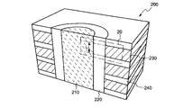
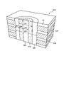
- FIG. 2 is a cross-sectional perspective view showing an element structure in the non-volatile storage device 100 according to the embodiment of the present invention. Specifically, FIG. 2 is an enlarged view of a portion surrounded by a frame line 200 (a portion corresponding to three non-volatile storage elements 20) in the non-volatile storage device 100.
- FIG. 3 is a perspective view showing the configuration of the semiconductor member 210 and the gate insulating layer 220 in the non-volatile storage element 20 shown in FIG. 2.
- the non-volatile storage element 20 of this embodiment is a FeFET composed of a semiconductor member 210, a gate insulating layer 220, and a gate electrode 230.
- the plurality of non-volatile storage elements 20 share the semiconductor member 210 and the gate insulating layer 220.
- the semiconductor member 210 is a columnar member that functions as a channel of the non-volatile memory element 20. As shown in FIGS. 2 and 3, the semiconductor member 210 has substantially no hollow portion or other member inside.
- substantially having no hollow portion or other member inside means that, for example, a minute hollow portion or other member may be included inside the semiconductor member 210. That is, a minute hollow portion or other member that does not significantly affect the element characteristics may be present inside the semiconductor member 210.
- the semiconductor member 210 is a continuous member from the outer peripheral surface to the central axis. That is, the semiconductor member 210 is continuously composed of the same material (including a material that can be regarded as substantially the same) from the outer peripheral surface to the central axis.
- IGZO is used as a material constituting the semiconductor member 210.
- IGZO is a metal oxide exhibiting semiconductor properties, and is a compound material composed of indium, gallium, zinc, and oxygen.
- IGZO is an oxide containing In, Ga and Zn, or a mixture of such oxides.
- the composition of IGZO is preferably In 2 -xGaxO 3 (ZnO) m (0 ⁇ x ⁇ 2, m is a natural number less than 0 or 6), and more preferably InGaO 3 (ZnO) m (m is 0). Or a natural number less than 6), most preferably InGaO 3 (ZnO).
- the semiconductor member 210 is cylindrical. However, the present invention is not limited to this example, and the semiconductor member 210 may be an elliptical columnar member or a prismatic columnar member. In the present embodiment, the diameter (D) of the semiconductor member 210 is 8 nm. The diameter of the semiconductor member 210 may be set in the range of, for example, 30 nm or less (preferably 1 nm or more and 20 nm or less, more preferably 4 nm or more and 10 nm or less).
- the diameter or length of the semiconductor member 210 in a direction substantially orthogonal to the interface between the semiconductor member 210 and the gate insulating layer 220 is set as the diameter of the semiconductor member 210. Just do it.
- a columnar semiconductor member 210 having a longitudinal direction in a direction substantially orthogonal to the substrate 110 is used.
- a hole having a diameter of 30 nm or less is filled with a metal oxide material to form a semiconductor member 210.
- the semiconductor member 210 is formed by using an ALD (Atomic Layer Deposition) method.
- the semiconductor member 210 uses a PLD (Pulsed Laser Deposition) method, a DC sputtering method, an RF sputtering method, a spin coating method, a dip coating method, a mist CVD (Mist Chemical Vapor Deposition) method, or the like. It is also possible to form. In particular, a method using a solution such as a spin coating method is suitable for filling the pores with a metal oxide material.
- the gate insulating layer 220 corresponds to the ferroelectric layer in the non-volatile storage element 20 of the present embodiment.
- hafnium oxide hereinafter referred to as “HZO”
- zirconium is added
- the present invention is not limited to this, and another ferroelectric layer such as hafnium oxide to which silicon, aluminum, gadolinium, yttrium, lanthanum, strontium or the like is added may be used as the gate insulating layer 220.
- the gate insulating layer 220 is formed with a film thickness of 10 nm by using an ALD (Atomic Layer Deposition) method.
- ALD Atomic Layer Deposition
- the film thickness of the gate insulating layer 220 is not limited to this example, and may be, for example, 5 nm or more and 22 nm or less (preferably 10 nm or more and 18 nm or less).
- the gate insulating layer 220 is provided so as to be in contact with the side surface of the semiconductor member 210 and surround the semiconductor member 210. That is, as shown in FIG. 3, the gate insulating layer 220 can be said to be a cylindrical member having a cylindrical semiconductor member 210 having a diameter (D) inside. As described above, the channel portion of the present embodiment has a structure in which the space inside the tubular gate insulating layer 220 is occupied by the semiconductor member 210.
- the gate electrode 230 functions as a gate for controlling the programming operation or the erasing operation of the non-volatile storage element 20.
- a compound layer made of titanium nitride (TiN) is used as the gate electrode 230.
- TiN titanium nitride
- the present invention is not limited to this, and as the material of the gate electrode 230, a metal material containing tungsten, tantalum, molybdenum, aluminum, copper and the like, or a compound material containing those metal materials can be used.
- the gate electrode 230 can be formed by, for example, a sputtering method.
- a technique called a gate first method or a gate last method can be used to form the gate electrode 230.
- the gate-first method a step of alternately laminating a polysilicon layer and an insulating layer such as silicon oxide on a substrate to form a laminate, and forming a plurality of holes in the vertical direction in the laminate to form the plurality of pores. After forming a strong dielectric layer inside the hole and then forming a channel layer (punch and plug), the polysilicon layer is used as it is as a gate electrode.
- the gate last method first, a step of alternately laminating a dummy layer made of silicon nitride or the like and an insulating layer such as silicon oxide to form a laminate, and a punch-and-plug step are performed. After that, a step of selectively removing the dummy layer and a step of embedding a metal material such as tungsten in the space formed by the removal are performed, and the metal layer made of the embedded metal material is used as a gate electrode.
- lithography and reactive ion etching can be used to form the pores.
- a CVD method or an ALD method can be used for embedding the space with a metal material.
- the width of the gate electrode 230 corresponds to the channel length (L) of the non-volatile storage element 20.
- the width of the gate electrode 230 is the film thickness of the titanium nitride layer that functions as the gate electrode 230.
- the width of the gate electrode 230 (that is, the channel length) is 1 ⁇ m or less (preferably 50 nm or less).
- the non-volatile storage element 20 of the present embodiment can secure a stable memory window when the channel length is 1 ⁇ m or less.
- the insulating layer 240 is an insulating film for insulatingly separating the two gate electrodes 230 adjacent to each other.
- an insulating film such as a silicon oxide film or a silicon nitride film can be used.
- the film thickness of the insulating layer 240 is 10 nm or more and 50 nm or less (preferably 20 nm or more and 40 nm or less), but the film thickness is not limited to this example.
- the film thickness of the insulating layer 240 may be appropriately determined according to the relationship with the channel length (that is, the width of the gate electrode 230).
- the film thickness of the insulating layer 240 is too thin, the adjacent non-volatile memory elements 20 may affect each other and cause a malfunction. Further, if the film thickness of the insulating layer 240 is too thick, the distance between the channels of the adjacent non-volatile storage elements 20 becomes long, which may be a barrier to carrier movement.
- the non-volatile storage device 100 of the present embodiment has a three-dimensional laminated structure in which a plurality of non-volatile storage elements 20 are integrated at high density. Further, since each non-volatile memory element 20 uses a metal oxide called IGZO as a channel, it has high reliability. IGZO has fewer internal defects than polysilicon, which is generally used as an FET channel, and is less likely to cause a decrease in carrier mobility. Further, since IGZO does not form an interface layer (low-k layer) having a low dielectric constant at the interface with the ferroelectric layer, it is possible to reduce the voltage loss that occurs when a voltage is supplied to the gate electrode.
- IGZO metal oxide
- IGZO has sufficient carrier mobility in the film-formed state (that is, in the amorphous state), so that it is not necessary to make it polycrystalline by annealing treatment, and it is affected by grain boundaries and crystal defects. None receive.
- the non-volatile storage element using IGZO as a channel can be operated as a junctionless FET (transistor without a pn junction). Therefore, the FET having IGZO as a channel has carriers moving in the channel body (near the center of the channel) and is not easily affected by the charge trap near the interface layer.
- the non-volatile storage element 20 of the present embodiment can realize high reliability by using IGZO as a channel. Further, as will be described later, in the non-volatile storage device 100 of the present embodiment, each non-volatile storage element 20 can operate with low power consumption. Therefore, according to the present embodiment, it is possible to obtain a non-volatile storage device 100 having a large capacity, low power consumption, and high reliability.
- the element characteristics of the non-volatile storage element 20 will be described using simulation results.
- FIG. 4 is a diagram showing a simulation result of Id-Vg characteristics in the non-volatile storage element 20 according to the embodiment of the present invention. Specifically, FIG. 4 shows the dependence of the Id-Vg characteristic on the channel length in FeFETs having the structures shown in FIGS. 2 and 3.
- FIG. 5 is a diagram showing the relationship between the width of the memory window and the channel length obtained from the Id-Vg characteristic of FIG.
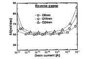
- FIG. 6 is a diagram showing the relationship between the SS value obtained from the Id-Vg characteristic of FIG. 4 and the drain current.
- the channel length (L) of the semiconductor member 210 was set to 10 nm, 20 nm, 50 nm, 100 nm, 200 nm, 500 nm, or 1 ⁇ m, respectively.
- the diameter of the semiconductor member 210 and the film thickness of the gate insulating layer 220 are set to 8 nm and 10 nm, respectively.
- the residual polarization (Pr) was set to 20 ⁇ C / cm 2 .
- the source-drain voltage (Vds) was set to 50 mV, and the source-gate voltage (hereinafter referred to as “gate voltage”) (Vg) was swept in the range of ⁇ 5 V to 5 V.
- the non-volatile storage element 20 of the present embodiment has a sufficient memory window if the channel length is 20 nm or more and 1 ⁇ m or less, and there is almost no change in the width of the memory window. I understood.
- the width of the memory window is 1.0 V or more and 1.3 V or less (specifically, 1.05 V or more and 1.25 V or less). ) Is stable. In other words, in the range where the channel length is 20 nm or more and 1 ⁇ m or less, the width of the memory window is within the range of 1.15 V ⁇ 1.0 V. As described above, the non-volatile storage element 20 of the present embodiment can secure a stable memory window width in a range of 20 nm or more and 1 ⁇ m or less without depending on the channel length.
- the non-volatile storage element 20 of the present embodiment when the channel length is less than 20 nm, the characteristics deteriorate like the so-called short channel effect due to the influence of the coupling between the source side potential and the drain side potential. Is considered to have occurred.
- the non-volatile storage element 20 of the present embodiment can obtain good switching operation at a low voltage of ⁇ 1.0 V or less regardless of the channel length in the range of the channel length of 1 ⁇ m or less. ing. In particular, in the range where the channel length is 20 nm or more and 1 ⁇ m or less, good switching operation is obtained at a low voltage of ⁇ 0.5 V or less. As described above, the non-volatile storage element 20 of the present embodiment has a feature of low power consumption because it can be operated at a low voltage.
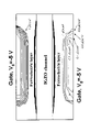
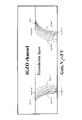
- FIG. 7 is a diagram showing the distribution of the polarization charge of the gate insulating layer 220 in the non-volatile storage element 20 according to the embodiment of the present invention.
- FIG. 8 is a diagram showing the distribution of the polarization charge of the gate insulating layer 220 in the non-volatile storage element 50 of Comparative Example 1.
- the gate voltage is set to ⁇ 5 V.
- the gate insulating layer (ferroelectric layer) is set as a continuum model.
- 7 and 8 show the dielectric polarization moment of the gate insulating layer in 0.2 ⁇ C / cm 2 steps when the channel length is 50 nm.
- the length of the long side of the rectangle described as “IGZO Channel” representing the channel corresponds to the channel length.
- spontaneous polarization reversal occurs continuously along the channel. That is, the spontaneous polarization of the gate insulating layer 220 in the non-volatile memory element 20 is continuously reversed from the source to the drain.
- the sign ( ⁇ ) of the spontaneous polarization is opposite on the upper side and the lower side of the channel, but it means that the vector direction of the electric field is opposite.
- a portion where spontaneous polarization inversion does not occur is observed at a position away from the channel, which is considered to be due to the fact that the ferroelectric layer is treated as a continuum model.
- the gate insulating layer 220 of the non-volatile storage element 20 continuously inverts the spontaneous polarization from the source side to the drain side, so that good write operation (program operation and erase operation) is controlled. It is possible.
- FIG. 8 shows the simulation result of FeFET having a planar structure using IGZO as a channel and a ferroelectric layer as a gate insulating layer.
- the reversal of the spontaneous polarization of the gate insulating layer is observed on the left side and the right side, but not near the center. That is, in the gate insulating layer in the non-volatile storage element of Comparative Example 1, the spontaneous polarization reversal occurs in the vicinity of the source and the drain, but the spontaneous polarization does not occur in the portion far from the source and the drain.
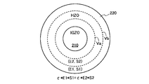
- FIG. 9 is a diagram showing a simulation model of the electric field distribution inside the gate insulating layer 220 in the non-volatile storage element 20 according to the embodiment of the present invention. Specifically, FIG. 9 shows the electric field distribution of the surface perpendicular to the longitudinal direction in the semiconductor member 210 and the gate insulating layer 220 shown in FIG.
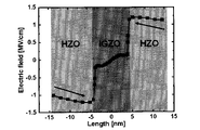
- FIG. 10 is a diagram showing a simulation result of the electric field distribution inside the gate insulating layer 220 in the non-volatile storage element 20 according to the embodiment of the present invention.
- FIG. 10 shows the electric field distribution in a straight line passing through the center point of the cross section perpendicular to the longitudinal direction in the semiconductor member 210 and the gate insulating layer 220 shown in FIG.
- the dotted lines schematically represent the equipotential lines Va and Vb, respectively.
- ⁇ , E and S represent the dielectric constant, the electric field strength and the surface area, respectively. That is, the electric field strength (electric field strength) inside the gate insulating layer 220 increases as it approaches the semiconductor member 210.
- FIG. 10 shows how the electric field strength inside the gate insulating layer 220 (region marked as HZO) increases as it approaches the semiconductor member 210 (region marked IGZO). Inside the gate insulating layer 220, a large electric field is formed in the vicinity of the semiconductor member 210 that functions as a channel. Therefore, as shown in FIG. 7, it is considered that spontaneous polarization reversal occurs continuously along the channel.
- the non-volatile memory element 20 of the present embodiment has a structure in which the columnar semiconductor member 210 is surrounded by the cylindrical gate insulating layer 220, so that the gate insulating layer 220 in the vicinity of the channel is spontaneously polarized. It has the feature that inversion is likely to occur. That is, in the present embodiment, it is possible to improve the characteristics of the program operation (particularly the erasing operation) by utilizing the fact that the electric field in the vicinity of the channel is strengthened by the electric field concentration in the three-dimensional structure.
- FIG. 11 is a diagram showing a simulation result of Id-Vg characteristics in the non-volatile storage element 20 according to the embodiment of the present invention. Specifically, FIG. 11 shows the dependence of the Id-Vg characteristic on the diameter of the semiconductor member 210 in the FeFET having the structures shown in FIGS. 2 and 3.
- FIG. 12 is a diagram showing the relationship between the width and the diameter of the memory window obtained from the Id-Vg characteristics shown in FIG.
- FIG. 13 is a diagram showing the relationship between the SS value obtained from the Id-Vg characteristic shown in FIG. 11 and the drain current.
- the diameter (D) of the semiconductor member 210 was set to 8 nm, 16 nm, or 24 nm, respectively.
- the channel length of the semiconductor member 210 and the film thickness of the gate insulating layer 220 are set to 50 nm and 10 nm, respectively.
- the residual polarization (Pr) was set to 20 ⁇ C / cm 2 .
- the source-drain voltage (Vds) was set to 50 mV, and the gate voltage (Vg) was swept in the range of ⁇ 5 V to 5 V.
- the diameter of the semiconductor member 210 in the non-volatile storage element 20 and the width of the memory window have a linear relationship.
- the diameter of the semiconductor member 210 is 20 nm or less, the width of the memory window of 0.6 V or more can be secured.
- the diameter of the semiconductor member 210 is 16 nm or less, the width of the memory window of 0.8 V or more can be secured.
- the diameter of the semiconductor member 210 is 10 nm or less, the width of the memory window of 1.0 V or more can be secured.
- the SS value of the non-volatile memory element 20 does not depend on the diameter of the semiconductor member 210 and falls within the range of 60 mV / dec or more and 65 mV / dec or less. It was also found that the SS value of the non-volatile memory element 20 decreases as the diameter of the semiconductor member 210 decreases. From the above, it was found that the SS value of the non-volatile memory element 20 shows a good value regardless of the diameter of the semiconductor member 210.
- the non-volatile storage element 20 of the present embodiment has a structure in which the inside of the cylindrical gate insulating layer 220 is occupied by the semiconductor member 210, as shown in FIGS. 2 and 3.
- the non-volatile storage element 20 has a good memory window in a range where the diameter (D) of the semiconductor member 210 is 20 nm or less and the channel length (L) is 1 ⁇ m or less, for example.
- the width and SS value can be obtained.
- FIG. 14 is a cross-sectional view showing an element structure in the non-volatile storage device 500 of Comparative Example 2.
- the non-volatile storage device 500 has a three-dimensional laminated structure in which a plurality of non-volatile storage elements 50 are three-dimensionally integrated.
- the plurality of non-volatile memory elements 50 are arranged in series along the longitudinal direction of the channel layer 510 in common with the cylindrical channel layer 510 that functions as a channel.
- the non-volatile memory element 50 is a FeFET composed of a channel layer 510, a gate insulating layer 520, and a gate electrode 530.
- the channel layer 510 and the gate insulating layer 520 are common to the plurality of non-volatile storage elements 50.
- the difference between the non-volatile memory element 20 of the present embodiment and the non-volatile memory element 50 shown in FIG. 14 is that the channel layer 510 of the non-volatile memory element 50 has a cylindrical shape, and the inside of the non-volatile memory element 50 is made of an insulating material.
- the point is that it has a filler member 550.
- the filler member 550 functions as a filling member that fills the inside of the cylindrical channel layer 510.
- an insulating material such as silicon oxide, silicon nitride, or resin can be used.
- the filler member 550 a member having a diameter of 4 nm and made of silicon oxide is used.
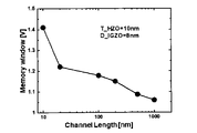
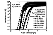
- FIG. 15 is a diagram showing a simulation result of the Id-Vg characteristic of the non-volatile storage element 50 of Comparative Example 2. Specifically, FIG. 15 shows the dependence of the Id-Vg characteristic on the channel length in the FeFET having the structure shown in FIG.
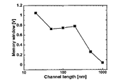
- FIG. 16 is a diagram showing the relationship between the width of the memory window and the channel length obtained from the Id-Vg characteristics shown in FIG.
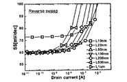
- FIG. 17 is a diagram showing the relationship between the SS value and the drain current obtained from the Id-Vg characteristics shown in FIG.
- the channel length (L) of the channel layer 510 was set to 20 nm, 50 nm, 100 nm, 200 nm, 500 nm, or 1 ⁇ m, respectively.
- the film thickness of the channel layer 510 and the film thickness of the gate insulating layer 520 were set to 8 nm and 10 nm, respectively.
- the residual polarization (Pr) was set to 20 ⁇ C / cm 2 .
- the source-drain voltage (Vds) was set to 50 mV and the gate voltage (Vg) was swept in the range of -5 V to 5 V.
- the memory window gradually opens in the range where the channel length is 500 nm or less, and the width of the memory window expands as the channel length becomes shorter.
- the width of the memory window is stable in the range of about 0.7 V or more and 0.8 V or less.
- the width of the memory window increased. This factor may be due to the influence of the coupling between the source side potential and the drain side potential.
- the SS value of the non-volatile storage element 50 of Comparative Example 2 did not depend on the channel length and was within about 60 mV / dec.
- the channel length was 20 nm, some deterioration was confirmed in the SS value.
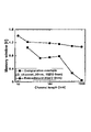
- FIG. 18 is a diagram comparing the dependence of the width of the memory window on the channel length between the non-volatile storage element 20 of the embodiment of the present invention and the non-volatile storage element 50 of Comparative Example 2.
- the plot represented by “Embodiment” shows the width of the memory window of the non-volatile storage element 20 of the present embodiment.
- the plot represented by “Comparative element” shows the width of the memory window of the non-volatile storage element 50 of Comparative Example 2.
- “D_channel_20 nm” means a structure in which a cylindrical IGZO having a film thickness of 8 nm is provided around a filler member having a diameter of 4 nm.
- the width of the memory window of the non-volatile storage element 20 according to the embodiment of the present invention is larger than the width of the memory window of the non-volatile storage element 50 of Comparative Example 2.
- the non-volatile storage element 50 of Comparative Example 2 has a large fluctuation in the width of the memory window, whereas the non-volatile storage element 20 of the present embodiment has a stable memory window width of about 1.2 V.
- the non-volatile storage element 20 of the present embodiment can stably secure a large memory window as compared with the non-volatile storage element 50 of Comparative Example 2 regardless of the channel length. That is, the non-volatile storage element 20 of the present embodiment can significantly improve the memory window as compared with the non-volatile storage element 50 of Comparative Example 2.
- Modification 1 In this modification, the relationship between the outer diameter of the semiconductor member 210 and the film thickness of the gate insulating layer 220 will be described.
- FIG. 19 is a cross-sectional perspective view showing a modified example of the element structure in the non-volatile storage device 100 according to the embodiment of the present invention. Specifically, FIG. 19 corresponds to an enlarged view of a portion surrounded by a frame line 200 in the non-volatile storage device 100 shown in FIG.
- the film thickness D2 of the gate insulating layer 220 composed of the ferroelectric substance is larger than the outer diameter D1 of the semiconductor member 210 (that is, the diameter of the semiconductor member 210). Specifically, when the outer diameter of the semiconductor member 210 is D1 and the film thickness of the gate insulating layer 220 is D2, the relationship of D1 ⁇ D2 is established. Such a relationship is derived from the simulation results described below.
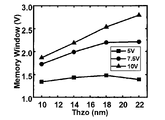
- FIG. 20 is a diagram showing the relationship between the width of the memory window and the film thickness of the gate insulating layer 220 (referred to as “Thso” in FIG. 20) in the non-volatile storage element having the element structure shown in FIG.
- the channel length and diameter of the semiconductor member 210 are set to 50 nm and 8 nm, respectively.
- the writing voltage was 5V, 7.5V and 10V.
- the width of the memory window gradually increases as the film thickness D2 of the gate insulating layer 220 increases regardless of the writing voltage. The tendency to become was observed.
- the width of the memory window decreases when the write voltage is 5 V, and the width of the memory window hardly changes when the write voltage is 7.5 V. I could't see it.
- the write voltage When the write voltage is 5 V, the tendency observed when the film thickness D2 of the gate insulating layer 220 exceeds 18 nm is that the write applied to the non-volatile storage element due to the increase in the film thickness of the gate insulating layer 220. It is probable that the voltage was insufficient. Therefore, when the write voltage is 10 V, the width of the memory window increases even if the film thickness D2 of the gate insulating layer 220 exceeds 18 nm. That is, it is considered that the higher the write voltage, the larger the film thickness of the gate insulating layer 220 at which the memory window reaches the maximum. However, since an increase in the write voltage causes an increase in the power consumption of the non-volatile storage device 100, it is desirable that the write voltage be 7.5 V or less.
- the width of the memory window linearly increases regardless of the write voltage when the film thickness D2 of the gate insulating layer 220 is at least 10 nm or more and 18 nm or less. Moreover, it was confirmed that a memory window having a width of at least 1.3 V or more can be secured. According to the results shown in FIG. 20, when each graph is extrapolated to the range where the film thickness D2 is 10 nm or less, the width is 1.3 V or more at least in the range where the film thickness D2 of the gate insulating layer 220 is 8 nm or more. It is expected that the memory window to be possessed can be secured.
- the film thickness D2 of the gate insulating layer 220 is equal to or larger than the outer diameter D1 (here, 8 nm) of the semiconductor member 210. More preferably, the film thickness D2 of the gate insulating layer 220 is 1.4 times or more the outer diameter D1 of the semiconductor member 210. That is, in the case of the example shown in FIG. 20, it is desirable that the film thickness D2 of the gate insulating layer 220 is 8 nm or more (preferably 12 nm or more, more preferably 16 nm or more).
- the film thickness D2 of the gate insulating layer 220 is made equal to the outer diameter D1 of the semiconductor member 210, or is made larger than the outer diameter D1 of the semiconductor member 210. Sufficient memory window width can be secured.
- the element structure shown in this modification is particularly effective when the diameter of the memory hole (cylindrical hole having a diameter of D3 in FIG. 19) is about 50 nm.
- the diameter of the memory hole (cylindrical hole having a diameter of D3 in FIG. 19) is about 50 nm.
- the smaller the outer diameter of the semiconductor member 210 the better the width of the memory window. Is obtained.
- the outer diameter of the semiconductor member 210 is inevitably large, which is not desirable from the viewpoint of securing the memory window.
- the element structure of this modification has a diameter of 50 nm while ensuring a memory window having a sufficient width by increasing the film thickness D2 of the gate insulating layer 220 while reducing the outer diameter D1 of the semiconductor member 210. It can sufficiently cope with a memory hole of a certain degree. Specifically, assuming that the diameter of the memory hole is in the range of 30 nm or more and 60 nm or less, the outer diameter of the semiconductor member 210 is 1 nm or more and 12 nm or less, and the film thickness of the gate insulating layer 220 is 15 nm or more and 22 nm or less. Is preferable.
- FIG. 21 is a cross-sectional perspective view showing a modified example of the element structure in the non-volatile storage device 100 according to the embodiment of the present invention. Specifically, FIG. 21 corresponds to an enlarged view of a portion surrounded by a frame line 200 in the non-volatile storage device 100 shown in FIG.
- the semiconductor member 210a has a cylindrical shape. That is, the semiconductor member 210a has a hollow portion in the center. In this modification, the hollow portion of the semiconductor member 210a is filled with the filler member 250a made of an insulating material. However, the present invention is not limited to this example, and the hollow portion of the semiconductor member 210a may be an empty void.
- the inner diameter D5 of the semiconductor member 210a (that is, the outer diameter of the filler member 250a) is sufficiently smaller than the outer diameter D1 of the semiconductor member 210a (that is, the diameter of the semiconductor member 210a).
- the ratio of the inner diameter D5 of the semiconductor member 210a to the outer diameter D1 of the semiconductor member 210a is 15% or less (preferably 10% or less). Such a relationship is derived from the simulation results described below.
- FIG. 22 is a diagram showing the relationship between the width of the memory window in the non-volatile storage element having the element structure shown in FIG. 21 and the film thickness D4 of the semiconductor member (referred to as “Tigzo” in FIG. 22).
- the channel length of the semiconductor member was set to 50 nm
- the film thickness of the gate insulating layer was set to 10 nm
- the write voltage was set to 5 V.
- the outer diameter D1 of the semiconductor member (simply referred to as “D” in FIG. 22) was set to 8 nm, 16 nm and 24 nm.
- the plot located at the right end corresponds to the element structure in which the semiconductor member has no hollow portion, that is, the element structure shown in FIG.
- all the plots other than the plot located at the right end correspond to the element structure in which the semiconductor member has a hollow portion (D5> 0) as shown in FIG. 21.
- the width of the memory window substantially equivalent to that of the element structure shown in FIG. 2 can be secured.
- the semiconductor member 210 is formed by filling a hole (trench) having a diameter of about 30 to 50 nm with a metal oxide material. At this time, from the inner wall side of the trench. As the filling progresses, a gap that cannot be filled may be formed in the vicinity of the center of the semiconductor member 210. However, even in this case, if the volume of the void is sufficiently small, it is considered that a memory window substantially equivalent to the case without the void can be secured.
- the width of the memory window is about 1.25 V.
- the diameter of the memory hole (cylindrical hole having a diameter of D3 in FIG. 23) is 36 nm.
- Such an element structure corresponds to the element structure of Comparative Example 2 shown in FIG. Specifically, referring to FIG.
- the outer diameter D1 of the semiconductor member 510 is 16 nm
- the film thickness D2 of the gate insulating layer 520 is 10 nm
- the diameter D3 of the memory hole is 36 nm
- the film thickness D4 of the semiconductor member 510 is 4 nm.
- the outer diameter D5 of the filler member 550 is 8 nm.
- the element structure in which the film thickness of the semiconductor member 210 (corresponding to half of the outer diameter D1 of the semiconductor member 210) and the diameter D3 of the memory hole are the same as the element structure shown in FIG.
- the outer diameter D1 of the semiconductor member 210 is 8 nm
- the film thickness D2 of the gate insulating layer 220 is 14 nm
- the diameter D3 of the memory hole is 36 nm.
- the width of the memory window of such an element structure is about 1.45V. That is, it is larger than the width of the memory window (about 1.25V) in the element structure shown in FIG. 23.
- the total thickness of the semiconductor members in the memory hole diameter D3 (D1 in the case of the element structure shown in FIG. 19 and twice D4 in the case of the element structure shown in FIG. 23).
- the element structure shown in FIG. 19 has a larger memory window width than the element structure shown in FIG. 23.
- Non-volatile storage element 110 ... Substrate, 120 ... Source electrode, 130 ... Drain electrode, 140 ... Source terminal, 150 ... Drain terminal, 160 ... Gate terminal, 170 ... Passion layer, 210 ... Semiconductor member, 220 ... Gate insulation Layer, 230 ... Gate electrode, 240 ... Insulation layer
Landscapes
- Non-Volatile Memory (AREA)
- Semiconductor Memories (AREA)
Abstract
Description
以下、本発明の一実施形態の不揮発性記憶装置100について説明する。
図4は、本発明の一実施形態の不揮発性記憶素子20におけるId-Vg特性のシミュレーション結果を示す図である。具体的には、図4は、図2及び図3に示した構造を有するFeFETにおけるチャネル長に対するId-Vg特性の依存性を示している。図5は、図4のId-Vg特性から求めたメモリウィンドウの幅とチャネル長との関係を示す図である。図6は、図4のId-Vg特性から求めたSS値とドレイン電流との関係を示す図である。
図14は、比較例2の不揮発性記憶装置500における素子構造を示す断面図である。図14に示すように、不揮発性記憶装置500は、複数の不揮発性記憶素子50が立体的に集積化した3次元積層構造を有する。複数の不揮発性記憶素子50は、チャネルとして機能する円筒状のチャネル層510を共通にして、チャネル層510の長手方向に沿って直列に配置される。不揮発性記憶素子50は、チャネル層510、ゲート絶縁層520、及びゲート電極530で構成されるFeFETである。チャネル層510及びゲート絶縁層520は、複数の不揮発性記憶素子50に対して共通である。本実施形態の不揮発性記憶素子20と、図14に示す不揮発性記憶素子50との相違点は、不揮発性記憶素子50は、チャネル層510が円筒形状であり、内側に絶縁材料で構成されるフィラー部材550を有する点である。フィラー部材550は、円筒形状のチャネル層510の内側を充填する充填部材として機能する。フィラー部材550としては、酸化シリコン、窒化シリコン、樹脂等の絶縁材料を用いることができる。本実施形態では、フィラー部材550として、酸化シリコンで構成される、直径4nmの部材を用いる。
本変形例では、半導体部材210の外径とゲート絶縁層220の膜厚との関係について説明する。
本変形例では、半導体部材の中心に、半導体部材の外径よりも十分に径の小さい中空部分が存在する例について説明する。
Claims (9)
- 複数の不揮発性記憶素子が直列に配置された3次元積層構造を有する不揮発性記憶装置であって、
金属酸化物を含む柱状の半導体部材と、
酸化ハフニウムを含み、前記半導体部材の側面に接して前記半導体部材を囲む強誘電体層と、
前記強誘電体層を介して前記半導体部材の側面に対向すると共に前記半導体部材の長手方向に沿って配置された複数のゲート電極と、
を備え、
前記半導体部材は、外周面から中心軸に至るまで連続する部材である、不揮発性記憶装置。 - 前記複数の不揮発性記憶素子は、前記半導体部材を共有する、請求項1に記載の不揮発性記憶装置。
- 前記半導体部材の直径が20nm以下である、請求項1又は2に記載の不揮発性記憶装置。
- 前記金属酸化物が、IGZO、ITO、IZO、又はITZOである、請求項1乃至3のいずれか一項に記載の不揮発性記憶装置。
- 前記複数のゲート電極の間にそれぞれ設けられた複数の絶縁層をさらに備える、請求項1乃至4のいずれか一項に記載の不揮発性記憶装置。
- 前記複数のゲート電極それぞれの幅が1μm以下である、請求項1乃至5のいずれか一項に記載の不揮発性記憶装置。
- 前記強誘電体層の膜厚が5nm以上20nm以下である、請求項1乃至6のいずれか一項に記載の不揮発性記憶装置。
- 前記強誘電体層の膜厚が前記半導体部材の外径以上である、請求項1乃至6のいずれか一項に記載の不揮発性記憶装置。
- 複数の不揮発性記憶素子が直列に配置された3次元積層構造を有する不揮発性記憶装置であって、
金属酸化物を含む円筒状の半導体部材と、
酸化ハフニウムを含み、前記半導体部材の側面に接して前記半導体部材を囲む強誘電体層と、
前記強誘電体層を介して前記半導体部材の側面に対向すると共に前記半導体部材の長手方向に沿って配置された複数のゲート電極と、
を備え、
前記半導体部材の外径に対する前記半導体部材の内径の割合が15%以下である、不揮発性記憶装置。
Priority Applications (4)
| Application Number | Priority Date | Filing Date | Title |
|---|---|---|---|
| KR1020237016235A KR20230110508A (ko) | 2020-12-04 | 2021-11-30 | 비휘발성 기억 장치 |
| JP2022566911A JP7849882B2 (ja) | 2020-12-04 | 2021-11-30 | 不揮発性記憶装置 |
| CN202180075646.4A CN116548079A (zh) | 2020-12-04 | 2021-11-30 | 非易失性存储装置 |
| US18/300,728 US20230255033A1 (en) | 2020-12-04 | 2023-04-14 | Ferroelectric memory device |
Applications Claiming Priority (2)
| Application Number | Priority Date | Filing Date | Title |
|---|---|---|---|
| JP2020-202180 | 2020-12-04 | ||
| JP2020202180 | 2020-12-04 |
Related Child Applications (1)
| Application Number | Title | Priority Date | Filing Date |
|---|---|---|---|
| US18/300,728 Continuation US20230255033A1 (en) | 2020-12-04 | 2023-04-14 | Ferroelectric memory device |
Publications (1)
| Publication Number | Publication Date |
|---|---|
| WO2022118809A1 true WO2022118809A1 (ja) | 2022-06-09 |
Family
ID=81853947
Family Applications (1)
| Application Number | Title | Priority Date | Filing Date |
|---|---|---|---|
| PCT/JP2021/043742 Ceased WO2022118809A1 (ja) | 2020-12-04 | 2021-11-30 | 不揮発性記憶装置 |
Country Status (6)
| Country | Link |
|---|---|
| US (1) | US20230255033A1 (ja) |
| JP (1) | JP7849882B2 (ja) |
| KR (1) | KR20230110508A (ja) |
| CN (1) | CN116548079A (ja) |
| TW (1) | TWI904291B (ja) |
| WO (1) | WO2022118809A1 (ja) |
Families Citing this family (2)
| Publication number | Priority date | Publication date | Assignee | Title |
|---|---|---|---|---|
| CN115701210B (zh) * | 2021-07-16 | 2025-07-04 | 长鑫存储技术有限公司 | 半导体结构及其制造方法 |
| CN116209344B (zh) * | 2023-02-10 | 2025-11-25 | 山东大学 | 基于铟铝锌氧化物的神经形态忆阻器、制备方法及设备 |
Citations (4)
| Publication number | Priority date | Publication date | Assignee | Title |
|---|---|---|---|---|
| JP2014053571A (ja) * | 2012-09-10 | 2014-03-20 | Toshiba Corp | 強誘電体メモリ及びその製造方法 |
| JP2016063027A (ja) * | 2014-09-17 | 2016-04-25 | 株式会社東芝 | 不揮発性半導体記憶装置及びその製造方法 |
| JP2020505790A (ja) * | 2017-01-20 | 2020-02-20 | リ, ウェイミンLI, Weimin | 強誘電体酸化物メモリデバイス |
| JP2020155644A (ja) * | 2019-03-20 | 2020-09-24 | キオクシア株式会社 | 半導体記憶装置 |
Family Cites Families (3)
| Publication number | Priority date | Publication date | Assignee | Title |
|---|---|---|---|---|
| US9634097B2 (en) | 2014-11-25 | 2017-04-25 | Sandisk Technologies Llc | 3D NAND with oxide semiconductor channel |
| WO2018144957A1 (en) * | 2017-02-04 | 2018-08-09 | Monolithic 3D Inc. | 3d semiconductor device and structure |
| US9941299B1 (en) * | 2017-05-24 | 2018-04-10 | Sandisk Technologies Llc | Three-dimensional ferroelectric memory device and method of making thereof |
-
2021
- 2021-11-30 CN CN202180075646.4A patent/CN116548079A/zh active Pending
- 2021-11-30 WO PCT/JP2021/043742 patent/WO2022118809A1/ja not_active Ceased
- 2021-11-30 KR KR1020237016235A patent/KR20230110508A/ko active Pending
- 2021-11-30 JP JP2022566911A patent/JP7849882B2/ja active Active
- 2021-12-03 TW TW110145251A patent/TWI904291B/zh active
-
2023
- 2023-04-14 US US18/300,728 patent/US20230255033A1/en active Pending
Patent Citations (4)
| Publication number | Priority date | Publication date | Assignee | Title |
|---|---|---|---|---|
| JP2014053571A (ja) * | 2012-09-10 | 2014-03-20 | Toshiba Corp | 強誘電体メモリ及びその製造方法 |
| JP2016063027A (ja) * | 2014-09-17 | 2016-04-25 | 株式会社東芝 | 不揮発性半導体記憶装置及びその製造方法 |
| JP2020505790A (ja) * | 2017-01-20 | 2020-02-20 | リ, ウェイミンLI, Weimin | 強誘電体酸化物メモリデバイス |
| JP2020155644A (ja) * | 2019-03-20 | 2020-09-24 | キオクシア株式会社 | 半導体記憶装置 |
Also Published As
| Publication number | Publication date |
|---|---|
| CN116548079A (zh) | 2023-08-04 |
| KR20230110508A (ko) | 2023-07-24 |
| JPWO2022118809A1 (ja) | 2022-06-09 |
| JP7849882B2 (ja) | 2026-04-22 |
| TWI904291B (zh) | 2025-11-11 |
| TW202243221A (zh) | 2022-11-01 |
| US20230255033A1 (en) | 2023-08-10 |
Similar Documents
| Publication | Publication Date | Title |
|---|---|---|
| US10714629B2 (en) | Transistor, semiconductor memory device, and method of manufacturing transistor | |
| US11765907B2 (en) | Ferroelectric memory device and operation method thereof | |
| EP3128534B1 (en) | Ferroelectric memory device and fabrication method thereof | |
| CN110854198B (zh) | 逻辑开关器件及其制造方法 | |
| US20150243658A1 (en) | Integrated circuits with varying gate structures and fabrication methods | |
| CN109671629B (zh) | 栅电极结构中的负电容匹配 | |
| CN108091693B (zh) | 铁电场效应晶体管及其制备方法 | |
| US12232434B2 (en) | Multi-doped data storage structure configured to improve resistive memory cell performance | |
| US8945997B2 (en) | Integrated circuits having improved split-gate nonvolatile memory devices and methods for fabrication of same | |
| TW201104846A (en) | Methods, devices, and systems relating to a memory cell having a floating body | |
| US11476254B2 (en) | Support pillars for vertical three-dimensional (3D) memory | |
| US9419078B2 (en) | Floating body memory with asymmetric channel | |
| US20230255033A1 (en) | Ferroelectric memory device | |
| Jeong et al. | All-sputter-deposited Hf 0.5 Zr 0.5 O 2 double-gate ferroelectric thin-film transistor with amorphous indium–gallium–zinc oxide channel | |
| TW202501830A (zh) | 薄膜電晶體 | |
| US20250176258A1 (en) | Semiconductor device including two-dimensional material | |
| US11462552B2 (en) | Semiconductor devices with memory cells | |
| US10043875B2 (en) | Spatially decoupled floating gate semiconductor device | |
| CN119096714A (zh) | 非易失性存储装置 | |
| US8921920B2 (en) | Semiconductor device | |
| US20260089916A1 (en) | Semiconductor device and semiconductor memory device | |
| US20230240063A1 (en) | Memory device | |
| US20240079495A1 (en) | Memory device and method of fabricating the same | |
| Huang et al. | Reconfigurable Logic and DRAM toward BEOL via Direct Deposition of High-k vdW Dielectric for 2D FETs | |
| Huang et al. | Direct Deposition of High-k van der Waals Dielectric for Top-Gated MoS 2 FETs Enabling Reconfigurable Logic and 2T0C DRAM toward BEOL-Compatible 3D Integration |
Legal Events
| Date | Code | Title | Description |
|---|---|---|---|
| 121 | Ep: the epo has been informed by wipo that ep was designated in this application |
Ref document number: 21900562 Country of ref document: EP Kind code of ref document: A1 |
|
| ENP | Entry into the national phase |
Ref document number: 2022566911 Country of ref document: JP Kind code of ref document: A |
|
| WWE | Wipo information: entry into national phase |
Ref document number: 202180075646.4 Country of ref document: CN |
|
| NENP | Non-entry into the national phase |
Ref country code: DE |
|
| 122 | Ep: pct application non-entry in european phase |
Ref document number: 21900562 Country of ref document: EP Kind code of ref document: A1 |