WO2022106943A1 - 半導体装置、表示装置、表示モジュール、及び電子機器 - Google Patents
半導体装置、表示装置、表示モジュール、及び電子機器 Download PDFInfo
- Publication number
- WO2022106943A1 WO2022106943A1 PCT/IB2021/060110 IB2021060110W WO2022106943A1 WO 2022106943 A1 WO2022106943 A1 WO 2022106943A1 IB 2021060110 W IB2021060110 W IB 2021060110W WO 2022106943 A1 WO2022106943 A1 WO 2022106943A1
- Authority
- WO
- WIPO (PCT)
- Prior art keywords
- layer
- insulating layer
- transistor
- semiconductor
- resin layer
- Prior art date
- Legal status (The legal status is an assumption and is not a legal conclusion. Google has not performed a legal analysis and makes no representation as to the accuracy of the status listed.)
- Ceased
Links
Images













Classifications
-
- H—ELECTRICITY
- H10—SEMICONDUCTOR DEVICES; ELECTRIC SOLID-STATE DEVICES NOT OTHERWISE PROVIDED FOR
- H10K—ORGANIC ELECTRIC SOLID-STATE DEVICES
- H10K59/00—Integrated devices, or assemblies of multiple devices, comprising at least one organic light-emitting element covered by group H10K50/00
- H10K59/10—OLED displays
- H10K59/12—Active-matrix OLED [AMOLED] displays
- H10K59/131—Interconnections, e.g. wiring lines or terminals
- H10K59/1315—Interconnections, e.g. wiring lines or terminals comprising structures specially adapted for lowering the resistance
-
- G—PHYSICS
- G09—EDUCATION; CRYPTOGRAPHY; DISPLAY; ADVERTISING; SEALS
- G09F—DISPLAYING; ADVERTISING; SIGNS; LABELS OR NAME-PLATES; SEALS
- G09F9/00—Indicating arrangements for variable information in which the information is built-up on a support by selection or combination of individual elements
- G09F9/30—Indicating arrangements for variable information in which the information is built-up on a support by selection or combination of individual elements in which the desired character or characters are formed by combining individual elements
-
- G—PHYSICS
- G09—EDUCATION; CRYPTOGRAPHY; DISPLAY; ADVERTISING; SEALS
- G09G—ARRANGEMENTS OR CIRCUITS FOR CONTROL OF INDICATING DEVICES USING STATIC MEANS TO PRESENT VARIABLE INFORMATION
- G09G3/00—Control arrangements or circuits, of interest only in connection with visual indicators other than cathode-ray tubes
- G09G3/20—Control arrangements or circuits, of interest only in connection with visual indicators other than cathode-ray tubes for presentation of an assembly of a number of characters, e.g. a page, by composing the assembly by combination of individual elements arranged in a matrix no fixed position being assigned to or needed to be assigned to the individual characters or partial characters
- G09G3/22—Control arrangements or circuits, of interest only in connection with visual indicators other than cathode-ray tubes for presentation of an assembly of a number of characters, e.g. a page, by composing the assembly by combination of individual elements arranged in a matrix no fixed position being assigned to or needed to be assigned to the individual characters or partial characters using controlled light sources
- G09G3/30—Control arrangements or circuits, of interest only in connection with visual indicators other than cathode-ray tubes for presentation of an assembly of a number of characters, e.g. a page, by composing the assembly by combination of individual elements arranged in a matrix no fixed position being assigned to or needed to be assigned to the individual characters or partial characters using controlled light sources using electroluminescent panels
- G09G3/32—Control arrangements or circuits, of interest only in connection with visual indicators other than cathode-ray tubes for presentation of an assembly of a number of characters, e.g. a page, by composing the assembly by combination of individual elements arranged in a matrix no fixed position being assigned to or needed to be assigned to the individual characters or partial characters using controlled light sources using electroluminescent panels semiconductive, e.g. using light-emitting diodes [LED]
- G09G3/3208—Control arrangements or circuits, of interest only in connection with visual indicators other than cathode-ray tubes for presentation of an assembly of a number of characters, e.g. a page, by composing the assembly by combination of individual elements arranged in a matrix no fixed position being assigned to or needed to be assigned to the individual characters or partial characters using controlled light sources using electroluminescent panels semiconductive, e.g. using light-emitting diodes [LED] organic, e.g. using organic light-emitting diodes [OLED]
- G09G3/3266—Details of drivers for scan electrodes
-
- G—PHYSICS
- G09—EDUCATION; CRYPTOGRAPHY; DISPLAY; ADVERTISING; SEALS
- G09G—ARRANGEMENTS OR CIRCUITS FOR CONTROL OF INDICATING DEVICES USING STATIC MEANS TO PRESENT VARIABLE INFORMATION
- G09G3/00—Control arrangements or circuits, of interest only in connection with visual indicators other than cathode-ray tubes
- G09G3/20—Control arrangements or circuits, of interest only in connection with visual indicators other than cathode-ray tubes for presentation of an assembly of a number of characters, e.g. a page, by composing the assembly by combination of individual elements arranged in a matrix no fixed position being assigned to or needed to be assigned to the individual characters or partial characters
- G09G3/22—Control arrangements or circuits, of interest only in connection with visual indicators other than cathode-ray tubes for presentation of an assembly of a number of characters, e.g. a page, by composing the assembly by combination of individual elements arranged in a matrix no fixed position being assigned to or needed to be assigned to the individual characters or partial characters using controlled light sources
- G09G3/30—Control arrangements or circuits, of interest only in connection with visual indicators other than cathode-ray tubes for presentation of an assembly of a number of characters, e.g. a page, by composing the assembly by combination of individual elements arranged in a matrix no fixed position being assigned to or needed to be assigned to the individual characters or partial characters using controlled light sources using electroluminescent panels
- G09G3/32—Control arrangements or circuits, of interest only in connection with visual indicators other than cathode-ray tubes for presentation of an assembly of a number of characters, e.g. a page, by composing the assembly by combination of individual elements arranged in a matrix no fixed position being assigned to or needed to be assigned to the individual characters or partial characters using controlled light sources using electroluminescent panels semiconductive, e.g. using light-emitting diodes [LED]
- G09G3/3208—Control arrangements or circuits, of interest only in connection with visual indicators other than cathode-ray tubes for presentation of an assembly of a number of characters, e.g. a page, by composing the assembly by combination of individual elements arranged in a matrix no fixed position being assigned to or needed to be assigned to the individual characters or partial characters using controlled light sources using electroluminescent panels semiconductive, e.g. using light-emitting diodes [LED] organic, e.g. using organic light-emitting diodes [OLED]
- G09G3/3275—Details of drivers for data electrodes
-
- H—ELECTRICITY
- H10—SEMICONDUCTOR DEVICES; ELECTRIC SOLID-STATE DEVICES NOT OTHERWISE PROVIDED FOR
- H10D—INORGANIC ELECTRIC SEMICONDUCTOR DEVICES
- H10D30/00—Field-effect transistors [FET]
- H10D30/01—Manufacture or treatment
- H10D30/021—Manufacture or treatment of FETs having insulated gates [IGFET]
-
- H—ELECTRICITY
- H10—SEMICONDUCTOR DEVICES; ELECTRIC SOLID-STATE DEVICES NOT OTHERWISE PROVIDED FOR
- H10D—INORGANIC ELECTRIC SEMICONDUCTOR DEVICES
- H10D30/00—Field-effect transistors [FET]
- H10D30/60—Insulated-gate field-effect transistors [IGFET]
- H10D30/67—Thin-film transistors [TFT]
- H10D30/6729—Thin-film transistors [TFT] characterised by the electrodes
- H10D30/673—Thin-film transistors [TFT] characterised by the electrodes characterised by the shapes, relative sizes or dispositions of the gate electrodes
- H10D30/6733—Multi-gate TFTs
- H10D30/6734—Multi-gate TFTs having gate electrodes arranged on both top and bottom sides of the channel, e.g. dual-gate TFTs
-
- H—ELECTRICITY
- H10—SEMICONDUCTOR DEVICES; ELECTRIC SOLID-STATE DEVICES NOT OTHERWISE PROVIDED FOR
- H10D—INORGANIC ELECTRIC SEMICONDUCTOR DEVICES
- H10D30/00—Field-effect transistors [FET]
- H10D30/60—Insulated-gate field-effect transistors [IGFET]
- H10D30/67—Thin-film transistors [TFT]
- H10D30/674—Thin-film transistors [TFT] characterised by the active materials
- H10D30/6755—Oxide semiconductors, e.g. zinc oxide, copper aluminium oxide or cadmium stannate
-
- H—ELECTRICITY
- H10—SEMICONDUCTOR DEVICES; ELECTRIC SOLID-STATE DEVICES NOT OTHERWISE PROVIDED FOR
- H10D—INORGANIC ELECTRIC SEMICONDUCTOR DEVICES
- H10D86/00—Integrated devices formed in or on insulating or conducting substrates, e.g. formed in silicon-on-insulator [SOI] substrates or on stainless steel or glass substrates
- H10D86/40—Integrated devices formed in or on insulating or conducting substrates, e.g. formed in silicon-on-insulator [SOI] substrates or on stainless steel or glass substrates characterised by multiple TFTs
- H10D86/421—Integrated devices formed in or on insulating or conducting substrates, e.g. formed in silicon-on-insulator [SOI] substrates or on stainless steel or glass substrates characterised by multiple TFTs having a particular composition, shape or crystalline structure of the active layer
- H10D86/423—Integrated devices formed in or on insulating or conducting substrates, e.g. formed in silicon-on-insulator [SOI] substrates or on stainless steel or glass substrates characterised by multiple TFTs having a particular composition, shape or crystalline structure of the active layer comprising semiconductor materials not belonging to the Group IV, e.g. InGaZnO
-
- H—ELECTRICITY
- H10—SEMICONDUCTOR DEVICES; ELECTRIC SOLID-STATE DEVICES NOT OTHERWISE PROVIDED FOR
- H10D—INORGANIC ELECTRIC SEMICONDUCTOR DEVICES
- H10D86/00—Integrated devices formed in or on insulating or conducting substrates, e.g. formed in silicon-on-insulator [SOI] substrates or on stainless steel or glass substrates
- H10D86/40—Integrated devices formed in or on insulating or conducting substrates, e.g. formed in silicon-on-insulator [SOI] substrates or on stainless steel or glass substrates characterised by multiple TFTs
- H10D86/441—Interconnections, e.g. scanning lines
-
- H—ELECTRICITY
- H10—SEMICONDUCTOR DEVICES; ELECTRIC SOLID-STATE DEVICES NOT OTHERWISE PROVIDED FOR
- H10D—INORGANIC ELECTRIC SEMICONDUCTOR DEVICES
- H10D86/00—Integrated devices formed in or on insulating or conducting substrates, e.g. formed in silicon-on-insulator [SOI] substrates or on stainless steel or glass substrates
- H10D86/40—Integrated devices formed in or on insulating or conducting substrates, e.g. formed in silicon-on-insulator [SOI] substrates or on stainless steel or glass substrates characterised by multiple TFTs
- H10D86/60—Integrated devices formed in or on insulating or conducting substrates, e.g. formed in silicon-on-insulator [SOI] substrates or on stainless steel or glass substrates characterised by multiple TFTs wherein the TFTs are in active matrices
-
- H—ELECTRICITY
- H10—SEMICONDUCTOR DEVICES; ELECTRIC SOLID-STATE DEVICES NOT OTHERWISE PROVIDED FOR
- H10K—ORGANIC ELECTRIC SOLID-STATE DEVICES
- H10K59/00—Integrated devices, or assemblies of multiple devices, comprising at least one organic light-emitting element covered by group H10K50/00
- H10K59/10—OLED displays
- H10K59/12—Active-matrix OLED [AMOLED] displays
- H10K59/124—Insulating layers formed between TFT elements and OLED elements
-
- G—PHYSICS
- G09—EDUCATION; CRYPTOGRAPHY; DISPLAY; ADVERTISING; SEALS
- G09G—ARRANGEMENTS OR CIRCUITS FOR CONTROL OF INDICATING DEVICES USING STATIC MEANS TO PRESENT VARIABLE INFORMATION
- G09G2300/00—Aspects of the constitution of display devices
- G09G2300/04—Structural and physical details of display devices
- G09G2300/0421—Structural details of the set of electrodes
- G09G2300/0426—Layout of electrodes and connections
-
- G—PHYSICS
- G09—EDUCATION; CRYPTOGRAPHY; DISPLAY; ADVERTISING; SEALS
- G09G—ARRANGEMENTS OR CIRCUITS FOR CONTROL OF INDICATING DEVICES USING STATIC MEANS TO PRESENT VARIABLE INFORMATION
- G09G2300/00—Aspects of the constitution of display devices
- G09G2300/04—Structural and physical details of display devices
- G09G2300/0421—Structural details of the set of electrodes
- G09G2300/043—Compensation electrodes or other additional electrodes in matrix displays related to distortions or compensation signals, e.g. for modifying TFT threshold voltage in column driver
-
- G—PHYSICS
- G09—EDUCATION; CRYPTOGRAPHY; DISPLAY; ADVERTISING; SEALS
- G09G—ARRANGEMENTS OR CIRCUITS FOR CONTROL OF INDICATING DEVICES USING STATIC MEANS TO PRESENT VARIABLE INFORMATION
- G09G2300/00—Aspects of the constitution of display devices
- G09G2300/08—Active matrix structure, i.e. with use of active elements, inclusive of non-linear two terminal elements, in the pixels together with light emitting or modulating elements
- G09G2300/0809—Several active elements per pixel in active matrix panels
- G09G2300/0819—Several active elements per pixel in active matrix panels used for counteracting undesired variations, e.g. feedback or autozeroing
-
- G—PHYSICS
- G09—EDUCATION; CRYPTOGRAPHY; DISPLAY; ADVERTISING; SEALS
- G09G—ARRANGEMENTS OR CIRCUITS FOR CONTROL OF INDICATING DEVICES USING STATIC MEANS TO PRESENT VARIABLE INFORMATION
- G09G3/00—Control arrangements or circuits, of interest only in connection with visual indicators other than cathode-ray tubes
- G09G3/20—Control arrangements or circuits, of interest only in connection with visual indicators other than cathode-ray tubes for presentation of an assembly of a number of characters, e.g. a page, by composing the assembly by combination of individual elements arranged in a matrix no fixed position being assigned to or needed to be assigned to the individual characters or partial characters
- G09G3/22—Control arrangements or circuits, of interest only in connection with visual indicators other than cathode-ray tubes for presentation of an assembly of a number of characters, e.g. a page, by composing the assembly by combination of individual elements arranged in a matrix no fixed position being assigned to or needed to be assigned to the individual characters or partial characters using controlled light sources
- G09G3/30—Control arrangements or circuits, of interest only in connection with visual indicators other than cathode-ray tubes for presentation of an assembly of a number of characters, e.g. a page, by composing the assembly by combination of individual elements arranged in a matrix no fixed position being assigned to or needed to be assigned to the individual characters or partial characters using controlled light sources using electroluminescent panels
- G09G3/32—Control arrangements or circuits, of interest only in connection with visual indicators other than cathode-ray tubes for presentation of an assembly of a number of characters, e.g. a page, by composing the assembly by combination of individual elements arranged in a matrix no fixed position being assigned to or needed to be assigned to the individual characters or partial characters using controlled light sources using electroluminescent panels semiconductive, e.g. using light-emitting diodes [LED]
- G09G3/3208—Control arrangements or circuits, of interest only in connection with visual indicators other than cathode-ray tubes for presentation of an assembly of a number of characters, e.g. a page, by composing the assembly by combination of individual elements arranged in a matrix no fixed position being assigned to or needed to be assigned to the individual characters or partial characters using controlled light sources using electroluminescent panels semiconductive, e.g. using light-emitting diodes [LED] organic, e.g. using organic light-emitting diodes [OLED]
- G09G3/3225—Control arrangements or circuits, of interest only in connection with visual indicators other than cathode-ray tubes for presentation of an assembly of a number of characters, e.g. a page, by composing the assembly by combination of individual elements arranged in a matrix no fixed position being assigned to or needed to be assigned to the individual characters or partial characters using controlled light sources using electroluminescent panels semiconductive, e.g. using light-emitting diodes [LED] organic, e.g. using organic light-emitting diodes [OLED] using an active matrix
- G09G3/3233—Control arrangements or circuits, of interest only in connection with visual indicators other than cathode-ray tubes for presentation of an assembly of a number of characters, e.g. a page, by composing the assembly by combination of individual elements arranged in a matrix no fixed position being assigned to or needed to be assigned to the individual characters or partial characters using controlled light sources using electroluminescent panels semiconductive, e.g. using light-emitting diodes [LED] organic, e.g. using organic light-emitting diodes [OLED] using an active matrix with pixel circuitry controlling the current through the light-emitting element
-
- H—ELECTRICITY
- H10—SEMICONDUCTOR DEVICES; ELECTRIC SOLID-STATE DEVICES NOT OTHERWISE PROVIDED FOR
- H10K—ORGANIC ELECTRIC SOLID-STATE DEVICES
- H10K2102/00—Constructional details relating to the organic devices covered by this subclass
- H10K2102/301—Details of OLEDs
- H10K2102/351—Thickness
Definitions
- One aspect of the present invention relates to a semiconductor device and a method for manufacturing the same.
- One aspect of the present invention relates to a display device.
- one aspect of the present invention is not limited to the above technical fields.
- the technical fields of one aspect of the present invention disclosed in the present specification and the like include semiconductor devices, display devices, light emitting devices, power storage devices, storage devices, electronic devices, lighting devices, input devices, input / output devices, and driving methods thereof. , Or their manufacturing methods, can be mentioned as an example.
- Semiconductor devices refer to all devices that can function by utilizing semiconductor characteristics.
- Oxide semiconductors using metal oxides are attracting attention as semiconductor materials applicable to transistors used in display devices.
- a plurality of oxide semiconductor layers are laminated, and among the plurality of oxide semiconductor layers, the oxide semiconductor layer serving as a channel contains indium and gallium, and the ratio of indium is the ratio of gallium.
- a semiconductor device having an increased electric field effect mobility by making it larger than the above is disclosed.
- One aspect of the present invention is to provide a display device in which the parasitic capacitance of wiring is reduced.
- One aspect of the present invention is to provide a display device having both high resolution and high frame frequency.
- One aspect of the present invention is to provide a high-definition display device.
- One aspect of the present invention is to provide a highly reliable display device or semiconductor device.
- One aspect of the present invention is to provide a semiconductor device, a display device, a display module, an electronic device, or the like having a novel configuration.
- One aspect of the present invention is to provide a method for manufacturing the above-mentioned display device or semiconductor device with high yield.
- One aspect of the present invention is to alleviate at least one of the problems of the prior art.
- One aspect of the present invention is a semiconductor device having a first wiring, a second wiring, and a transistor.
- the semiconductor device has a first resin layer between the first wiring and the transistor.
- the semiconductor device has a first insulating layer between the first resin layer and the transistor.
- the semiconductor device has a second resin layer between the transistor and the second wiring.
- the semiconductor device has a second insulating layer between the second resin layer and the transistor.
- the first insulating layer and the second insulating layer have an inorganic insulating film containing nitrogen.
- the first resin layer and the second resin layer have a lower dielectric constant than the first insulating layer and the second insulating layer, respectively. Further, the thickness of the first resin layer and the second resin layer is 5 times or more and 100 times or less as thick as those of the first insulating layer and the second insulating layer, respectively.
- the first resin layer and the second resin layer contain the same material and have the same thickness.
- the thickness of the second resin layer is preferably 80% or more and 120% or less of the thickness of the first resin layer.
- the first resin layer and the second resin layer are formed by the same film forming method using the same material.
- the first insulating layer and the second insulating layer contain the same material and have the same thickness.
- the thickness of the second insulating layer is preferably 80% or more and 120% or less of the thickness of the first insulating layer.
- the first insulating layer and the second insulating layer are formed by the same film forming method using the same material.
- the transistor has a first gate electrode, a second gate electrode, a first gate insulating layer, a second gate insulating layer, and a semiconductor layer.
- the first gate insulating layer is located between the semiconductor layer and the first gate electrode.
- the second gate insulating layer is located between the semiconductor layer and the second gate electrode.
- the first gate electrode and the second gate electrode have an overlapping region via the semiconductor layer.
- the first gate electrode is electrically connected to the first wiring at the openings provided in the first insulating layer and the first resin layer.
- the second wiring is electrically connected to the semiconductor layer at the openings provided in the second resin layer and the second insulating layer.
- the transistor has a first electrode between the second resin layer and the second insulating layer. Further, it is preferable that the first electrode is electrically connected to a part of the semiconductor layer at the opening provided in the second insulating layer. Further, it is preferable that the second wiring is electrically connected to the first electrode at the opening provided in the second resin layer.
- the second gate electrode is electrically connected to the first gate electrode at the openings provided in the first gate insulating layer and the second gate insulating layer. ..
- the semiconductor layer contains either or both of indium and zinc and oxygen.
- the semiconductor layer contains indium, gallium, and zinc, and the semiconductor layer has an atomic number ratio of indium more than twice that of gallium and a zinc atomic number ratio of more than twice that of gallium. It is more preferable to have.
- the first resin layer and the second resin layer each contain acrylic or polyimide.
- one aspect of the present invention is a display device having any of the above semiconductor devices, a pixel electrode, a source drive circuit, and a gate drive circuit. Further, it is preferable that the display device has a third resin layer between the pixel electrode and the transistor. Further, it is preferable that the first wiring is electrically connected to the source drive circuit and the second wiring is electrically connected to the gate drive circuit.
- the pixel electrode is preferably an electrode of an organic EL element.
- one aspect of the present invention is a display module having any of the above display devices and a connector or an integrated circuit.
- one aspect of the present invention is an electronic device having the above-mentioned display module and at least one of an antenna, a battery, a housing, a camera, a speaker, a microphone, a touch sensor, and an operation button.
- a display device in which the parasitic capacitance of wiring is reduced.
- a display device having both high resolution and high frame frequency Alternatively, a high-definition display device can be provided.
- a highly reliable display device or semiconductor device can be provided.
- a semiconductor device a display device, a display module, an electronic device, or the like having a novel configuration.
- at least one of the problems of the prior art can be alleviated.
- 1A to 1C are diagrams showing a configuration example of a semiconductor device.
- 2A and 2B are diagrams showing a configuration example of a semiconductor device.
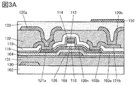
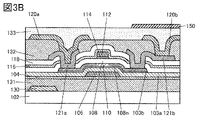
- 3A and 3B are diagrams showing a configuration example of a semiconductor device.
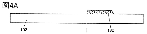
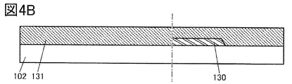
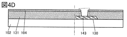
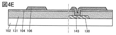
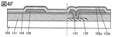
- 4A to 4F are diagrams illustrating an example of a method for manufacturing a semiconductor device.
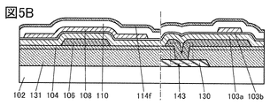
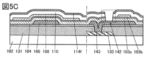
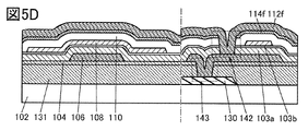
- 5A to 5D are diagrams illustrating an example of a method for manufacturing a semiconductor device.
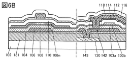
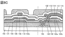
- 6A to 6C are diagrams illustrating an example of a method for manufacturing a semiconductor device.
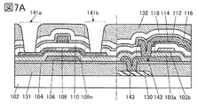
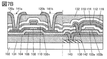
- 7A and 7B are diagrams illustrating an example of a method for manufacturing a semiconductor device.
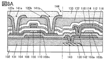
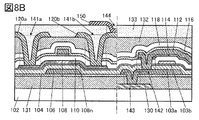
- 8A and 8B are diagrams illustrating an example of a method for manufacturing a semiconductor device.
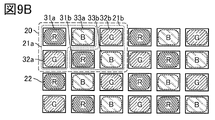
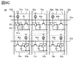
- 9A to 9C are diagrams showing a configuration example of the display device.
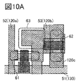
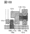
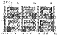
- FIGS. 10A to 10C are diagrams showing a configuration example of pixels.
- FIG. 11 is a diagram showing a configuration example of the display device.
- FIG. 12 is a diagram showing a configuration example of the display device.
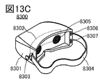
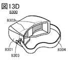
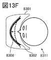
- 13A to 13F are views showing a configuration example of an electronic device.
- 14A and 14B are diagrams showing a configuration example of a display module.
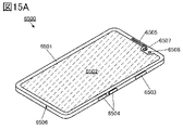
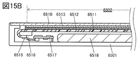
- 15A and 15B are diagrams showing a configuration example of an electronic device.
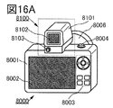
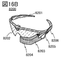
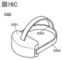
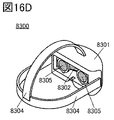
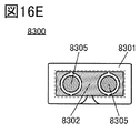
- 16A to 16E are diagrams showing a configuration example of an electronic device.
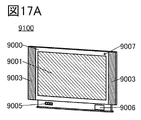
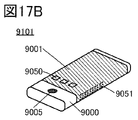
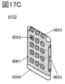
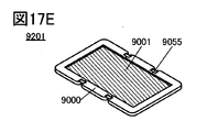
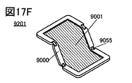
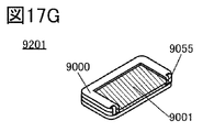
- 17A to 17G are diagrams showing a configuration example of an electronic device.
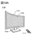
- 18A to 18D are diagrams showing a configuration example of an electronic device.
- a transistor is a kind of semiconductor element, and can realize a function of amplifying a current or a voltage and a switching operation for controlling conduction or non-conduction.
- the transistor in the present specification includes an IGFET (Insulated Gate Field Transistor) and a thin film transistor (TFT: Thin Film Transistor).
- source and drain functions may be interchanged when transistors with different polarities are used, or when the direction of current changes during circuit operation. Therefore, in the present specification, the terms “source” and “drain” may be used interchangeably.
- membrane and the term “layer” can be interchanged with each other.
- conductive layer or “insulating layer” may be interchangeable with the terms “conductive film” or “insulating film”.
- the display panel which is one aspect of the display device, has a function of displaying (outputting) an image or the like on the display surface. Therefore, the display panel is an aspect of the output device.
- a connector such as FPC (Flexible Printed Circuit) or TCP (Tape Carrier Package) is attached to the board of the display panel, or an IC is used on the board by a COG (Chip On Glass) method or the like.
- FPC Flexible Printed Circuit
- TCP Transmission Carrier Package
- COG Chip On Glass
- Embodiment 1 a semiconductor device according to one aspect of the present invention, a method for manufacturing the semiconductor device, a display device, and the like will be described.
- a transistor using an oxide semiconductor in the semiconductor layer on which the channel is formed will be described.
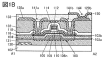
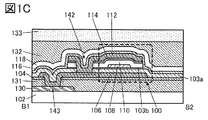
- FIG. 1A shows a schematic top view of a semiconductor device including the transistor 100. Further, FIG. 1B corresponds to a cross-sectional view of the alternate long and short dash line A1-A2 shown in FIG. 1A, and FIG. 1C corresponds to a cross-sectional view of the alternate long and short dash line B1-B2 shown in FIG. 1A. In FIG. 1A, a part of the components (gate insulating layer, etc.) is omitted. 1B is a cross-sectional view of the transistor 100 in the channel length direction, and FIG. 1C is a cross-sectional view including a cross section in the channel width direction.
- the transistor 100 is provided on the substrate 102 and has a conductive layer 106, an insulating layer 103a, an insulating layer 103b, a semiconductor layer 108, an insulating layer 110, a metal oxide layer 114, a conductive layer 112, and the like. Further, a resin layer 131 is provided between the transistor 100 and the substrate 102. A resin layer 132 is provided on the transistor 100. An insulating layer 104 is provided between the resin layer 131 and the transistor 100. An insulating layer 116 and an insulating layer 118 are laminated and provided between the transistor 100 and the resin layer 132.
- a part of the conductive layer 106 and a part of the conductive layer 112 each function as a gate electrode. Further, a part of the insulating layer 103a, a part of the insulating layer 103b, and a part of the insulating layer 110 each function as a gate insulating layer.
- a conductive layer 130 that functions as wiring is provided between the substrate 102 and the resin layer 131. Further, a conductive layer 120a and a conductive layer 120b are provided on the resin layer 132. At least one of the conductive layer 120a and the conductive layer 120b functions as wiring.
- the resin layer 133 is provided so as to cover the resin layer 132, the conductive layer 120a, and the conductive layer 120b. Further, a conductive layer 150 is provided on the resin layer 133.
- the conductive layer 150 can be used, for example, as a pixel electrode of a display element. Alternatively, the conductive layer 150 may be used as wiring.
- the conductive layer 150 is electrically connected to the conductive layer 120b at the opening 144 provided in the resin layer 133.
- the insulating layer 104 functions as a barrier membrane that prevents impurities such as water and hydrogen in the resin layer 131 from diffusing into the transistor 100.
- the insulating layer 116 also functions as a barrier membrane that prevents impurities such as water and hydrogen contained in the resin layer 132 from diffusing into the transistor 100.
- an inorganic insulating film in which water or hydrogen does not easily diffuse can be used.
- an insulating film containing a nitride such as silicon nitride, silicon nitride oxide, silicon nitride nitride, aluminum nitride, and aluminum nitride can be preferably used.
- silicon nitride since silicon nitride has a blocking property against either one or both of hydrogen and oxygen, it can prevent both the diffusion of hydrogen from the outside to the semiconductor layer 108 and the desorption of oxygen from the semiconductor layer 108 to the outside. It is possible to realize a highly reliable transistor.
- Organic resin can be used for the resin layer 131 and the resin layer 132.
- acrylic or polyimide it is preferable to use acrylic or polyimide.
- the material that can be used for the resin layer 131 is not limited to this, and a chemically or thermally stable material can be used.
- the resin layer 131 and the resin layer 132 preferably function as a flattening film.
- a film formed by a coating method such as a spin coating method or a slit coating method is preferable. Since the resin layer 131 functions as a flattening film, the influence of the step due to the conductive layer 130 located closer to the substrate 102 than the transistor 100 can be suppressed, the formed surface of the transistor 100 can be flattened, and the electrical characteristics of the transistor 100 can be improved. Variation can be reduced. Further, since the resin layer 132 functions as a flattening film, the influence of the step due to the transistor 100 can be suppressed, the formed surfaces of the conductive layer 120a and the conductive layer 120b can be flattened, and processing defects thereof can be reduced. Further, since the formed surface of the conductive layer 150 that can be used as a pixel electrode or the like can be flattened, it is possible to reduce variations in the electrical characteristics and optical characteristics of the display element that uses the conductive layer 150 as the pixel electrode.
- the resin layer 131 and the resin layer 132 each have a low dielectric constant. Specifically, it is preferable to use an organic insulating material having a lower dielectric constant than either or both of the insulating layer 104 and the insulating layer 116. In particular, it is preferable that the resin layer 131 and the resin layer 132 have a lower dielectric constant than both the insulating layer 104 and the insulating layer 116.
- the resin layer 131 and the resin layer 132 are each thickly formed.
- the resin layer 131 and the resin layer 132 are thicker than either or both of the insulating layer 104 and the insulating layer 116, respectively.
- the resin layer 131 and the resin layer 132 are thicker than both the insulating layer 104 and the insulating layer 116.
- the thickness of the resin layer 131 and the resin layer 132 is 5 times or more and 100 times or less, or 5 times or more and 50 times or less, or 5 times or more and 30 times or less, respectively, as thick as the insulating layer 104 or the insulating layer 116. Can be.
- the insulating layer 104 and the insulating layer 116 may have a thickness of 50 nm or more and 300 nm or less, and the resin layer 131 and the resin layer 132 may have a thickness of 500 nm or more and 20 ⁇ m or less, preferably 1 ⁇ m or more and 10 ⁇ m or less. can.
- FIG. 1B shows a cross section at the intersection of the conductive layer 130 and the conductive layer 120a shown in FIG. 1A.
- At least a resin layer 131 and a resin layer 132 are provided between the conductive layer 130 and the conductive layer 120a. Since the resin layer 131 and the resin layer 132 are layers having a low dielectric constant and formed thickly, the capacitance generated between them at the intersection of the conductive layer 130 and the conductive layer 120a should be extremely small. Can be done. This makes it possible to realize a display device that can be driven at a high resolution, a high definition, and a high frame rate.
- the resolution is full high definition (also called “2K resolution”, “2K1K”, or “2K”), ultra high definition (also called “4K resolution”, “4K2K”, or “4K”) or super high definition ("8K resolution”). , “8K4K”, or “8K”).
- the fineness is, for example, 400 ppi or more, or 500 ppi or more, preferably 1000 ppi or more, more preferably 2000 ppi or more, further 3000 ppi or more, and a high-definition display having a fineness of 10,000 ppi or less, 7500 ppi or less, or 6000 ppi or less.
- the device can be realized. It should be noted that even for a display device having a definition of less than 400 ppi, it is preferable because the parasitic capacitance can be reduced by applying the above configuration. For example, the above configuration can be suitably used for a large display device having a screen diagonal size of 50 inches or more, 60 inches or more, or 70 inches or more.
- the time constant of the wiring can be reduced, the time required for charging and discharging the wiring (for example, the writing time of the pixel) can be shortened, so that it is possible to drive at a high frame rate. For example, 60Hz drive, 120Hz drive, 180Hz drive, and even 240Hz drive can be expected.
- the resin layer 131 and the resin layer 132 contain the same material and have the same thickness.
- the thickness of the resin layer 132 is preferably 80% or more and 120% or less of the thickness of the resin layer 131.
- the resin layer 131 and the resin layer 132 are formed by the same film forming method using the same material.
- the stress can be made the same.
- the stress can be made similar between the upper and lower parts of the transistor 100, so that an extreme stress difference does not occur, and as a result, film peeling during the process can be suppressed.
- the stress applied to the transistor 100 from above and below can be made uniform, variations in the electrical characteristics of the transistor 100 can be reduced.
- the insulating layer 104 and the insulating layer 116 also contain the same material and have the same thickness.
- the thickness of the insulating layer 116 is preferably 80% or more and 120% or less of the thickness of the insulating layer 104.
- the insulating layer 104 and the insulating layer 116 are formed by the same film forming method using the same material. As a result, not only the film peeling during the process can be suppressed more effectively, but also the variation in the electrical characteristics of the transistor 100 can be reduced.
- the conductive layer 106 is provided on the insulating layer 104.
- the insulating layer 103a is provided so as to cover the conductive layer 106.
- the insulating layer 103b is provided on the insulating layer 103a.
- the island-shaped semiconductor layer 108 is provided on the insulating layer 103b and overlaps with a part of the conductive layer 106.
- the insulating layer 110, the metal oxide layer 114, and the conductive layer 112 are provided on the semiconductor layer 108 and the insulating layer 103b in this order, and have a portion that overlaps with the semiconductor layer 108 and the conductive layer 106.
- the insulating layer 116 is provided so as to cover the insulating layer 103a, the semiconductor layer 108, the insulating layer 110, the metal oxide layer 114, and the conductive layer 112.
- the insulating layer 118 is provided on the insulating layer 116.
- the semiconductor layer 108 has a region that overlaps with the conductive layer 112 and a pair of low resistance regions 108n that sandwich the region.
- the region of the semiconductor layer 108 that overlaps with the conductive layer 112 functions as a channel forming region of the transistor 100.
- the pair of low resistance regions 108n function as a source region and a drain region of the transistor 100.
- the insulating layer 103a and the insulating layer 103b are continuously formed by using a plasma CVD apparatus without being exposed to the atmosphere.
- an insulating film containing nitrogen such as a silicon nitride film, a silicon nitride film, an aluminum nitride film, and a hafnium nitride film can be used.
- the insulating layer 103b in contact with the semiconductor layer 108 is preferably a dense insulating film in which impurities such as water are not easily adsorbed on the surface thereof. Further, it is preferable to use an insulating film having as few defects as possible and reduced impurities such as water or hydrogen.
- Examples of the insulating layer 103b include a silicon oxide film, a silicon nitride film, a silicon nitride film, an aluminum oxide film, a hafnium oxide film, an yttrium oxide film, a zirconium oxide film, a gallium oxide film, a tantalum oxide film, and a magnesium oxide film.
- An insulating layer containing one or more of a lanthanum oxide film, a cerium oxide film, and a neodymium oxide film can be used. In particular, it is preferable to use a silicon oxide film or a silicon nitride film.
- the insulating layer 103b in contact with the semiconductor layer 108 preferably has an oxide insulating film. Further, it is more preferable that the insulating layer 103b has a region containing oxygen in excess of the stoichiometric composition. In other words, the insulating layer 103b has an insulating film capable of releasing oxygen. For example, forming the insulating layer 103b in an oxygen atmosphere, heat-treating the insulating layer 103b after film formation in an oxygen atmosphere, plasma treatment in an oxygen atmosphere after forming the insulating layer 110, etc.
- an oxide film for example, a metal oxide film to be the semiconductor layer 108
- oxygen can be supplied to the insulating layer 103b. ..
- an oxidizing gas for example, nitrous oxide, ozone, etc. may be used instead of or in addition to oxygen.
- the semiconductor layer 108 contains a metal oxide exhibiting semiconductor characteristics (hereinafter, also referred to as an oxide semiconductor).
- the semiconductor layer 108 preferably contains at least indium and oxygen. Since the semiconductor layer 108 contains an oxide of indium, the carrier mobility can be enhanced. For example, it is possible to realize a transistor capable of passing a larger current than when amorphous silicon is used.
- the region of the semiconductor layer 108 that overlaps the conductive layer 112 functions as a channel forming region. Further, the semiconductor layer 108 preferably has a pair of low resistance regions 108n with the channel forming region interposed therebetween.
- the low resistance region 108n is a region having a higher carrier concentration than the channel formation region, and functions as a source region and a drain region.
- the low resistance region 108n can also be said to be a region having a lower resistance, a region having a high carrier concentration, a region having a large amount of oxygen deficiency, a region having a high hydrogen concentration, or a region having a high impurity concentration than the channel forming region.
- the semiconductor layer 108 preferably contains at least a metal oxide containing indium and oxygen. Further, the semiconductor layer 108 may contain zinc in addition to these. Further, the semiconductor layer 108 may contain gallium.
- indium oxide indium zinc oxide (In-Zn oxide), indium gallium zinc oxide (also referred to as In-Ga-Zn oxide, IGZO) and the like can be typically used.
- indium tin oxide In—Sn oxide
- indium tin oxide containing silicon or the like can also be used.
- the composition of the semiconductor layer 108 greatly affects the electrical characteristics, reliability, and the like of the transistor 100. For example, by increasing the content of indium in the semiconductor layer 108, carrier mobility is improved, and a transistor having high field effect mobility can be realized.
- GBT Gate Bias Stress Test
- PBTS Positive Bias Temperature Stress
- the PBTS test and the NBTS test conducted in a state of being irradiated with light such as white LED light are called PBTIS (Positive Bias Temperature Illumination Stress) test and NBTIS (Negative Bias Temperature Test) Test, respectively.
- the composition of the semiconductor layer 108 preferably has a smaller gallium content than the indium content. This makes it possible to realize a highly reliable transistor.
- a metal oxide film in which the atomic number ratio of In is higher than the atomic number ratio of Ga is applied to the semiconductor layer 108.
- the semiconductor layer 108 is preferably a film formed by a sputtering method using a metal oxide target in which the atomic number ratio of the metal element is in the above range. At this time, the composition of the semiconductor layer 108 after the film formation may deviate from the composition of the metal oxide target.
- a metal oxide film containing no gallium may be applied to the semiconductor layer 108.
- the In—Zn oxide can be applied to the semiconductor layer 108.
- the electric field effect mobility of the transistor can be increased by increasing the atomic number ratio of In to the atomic number of the metal element contained in the metal oxide film.
- a highly crystalline metal oxide film is obtained, so that fluctuations in the electrical characteristics of the transistor are suppressed and reliability is improved.
- a metal oxide film containing no gallium and zinc such as indium oxide may be applied to the semiconductor layer 108.
- an oxide film such as indium oxide, indium zinc oxide, or indium tin oxide can be used for the semiconductor layer 108.
- M is aluminum, silicon, boron, yttrium, tin, copper, vanadium, beryllium, titanium, iron, nickel, germanium, zirconium, molybdenum
- M is preferably one or more selected from gallium, aluminum, yttrium, or tin.
- a crystalline metal oxide film for the semiconductor layer 108 It is preferable to use a crystalline metal oxide film for the semiconductor layer 108.
- a metal oxide film having a CAAC (c-axis aligned crystal) structure, a polycrystalline structure, a microcrystal structure, etc., which will be described later, can be used.
- CAAC c-axis aligned crystal
- the defect level density in the semiconductor layer 108 can be reduced, and a highly reliable semiconductor device can be realized.
- the low resistance region 108n of the semiconductor layer 108 is a region containing an impurity element.
- the impurity element include hydrogen, boron, carbon, nitrogen, fluorine, phosphorus, sulfur, arsenic, aluminum, and rare gas.
- the noble gas include helium, neon, argon, krypton, xenon and the like. In particular, it preferably contains boron or phosphorus. Further, it may contain two or more of these elements.
- the impurity concentration is 1 ⁇ 10 19 atoms / cm 3 or more, 1 ⁇ 10 23 atoms / cm 3 or less, preferably 5 ⁇ 10 19 atoms / cm 3 or more, and 5 ⁇ 10 22 atoms / cm 3
- the concentration of impurities contained in the low resistance region 108n is analyzed by, for example, an analysis method such as secondary ion mass spectrometry (SIMS: Secondary Ion Mass Spectrometry) or X-ray photoelectron spectroscopy (XPS: X-ray Photoelectron Spectroscopy).
- an analysis method such as secondary ion mass spectrometry (SIMS: Secondary Ion Mass Spectrometry) or X-ray photoelectron spectroscopy (XPS: X-ray Photoelectron Spectroscopy).
- SIMS Secondary Ion Mass Spectrometry
- XPS X-ray Photoelectron Spectroscopy
- the conductive layer 112, the metal oxide layer 114, and the insulating layer 110 are processed so that their upper surface shapes substantially match each other.
- the top surface shapes are substantially the same.
- the contours do not overlap, and the upper layer may be located inside the lower layer, or the upper layer may be located outside the lower layer. In this case as well, it is said that the top surface shapes are roughly the same.
- the description of the insulating layer 103b can be incorporated.
- the metal oxide layer 114 located between the insulating layer 110 and the conductive layer 112 functions as a barrier membrane for preventing oxygen contained in the insulating layer 110 from diffusing toward the conductive layer 112. Further, the metal oxide layer 114 also functions as a barrier membrane for preventing hydrogen or water contained in the conductive layer 112 from diffusing toward the insulating layer 110.
- the metal oxide layer 114 for example, it is preferable to use a material that is less permeable to oxygen and hydrogen than the insulating layer 110.
- the metal oxide layer 114 can prevent oxygen from diffusing from the insulating layer 110 to the conductive layer 112 even when a metal material such as aluminum or copper that easily absorbs oxygen is used for the conductive layer 112. .. Further, even when the conductive layer 112 contains hydrogen, it is possible to prevent hydrogen from diffusing from the conductive layer 112 to the semiconductor layer 108 via the insulating layer 110. As a result, the carrier density in the channel formation region of the semiconductor layer 108 can be made extremely low.
- the metal oxide layer 114 an insulating material or a conductive material can be used.
- the metal oxide layer 114 functions as a part of the gate insulating layer.
- the metal oxide layer 114 has conductivity, the metal oxide layer 114 functions as a part of the gate electrode.
- the metal oxide layer 114 it is preferable to use an insulating material having a higher dielectric constant than silicon oxide.
- an aluminum oxide film, a hafnium oxide film, a hafnium aluminate film, or the like because the driving voltage can be reduced.
- a conductive oxide such as indium oxide, indium tin oxide (ITO), or silicon-containing indium tin oxide (ITSO) can also be used.
- ITO indium tin oxide
- ITSO silicon-containing indium tin oxide
- conductive oxides containing indium are preferable because they have high conductivity.
- the metal oxide layer 114 it is preferable to use an oxide material containing one or more of the same elements as the semiconductor layer 108. In particular, it is preferable to use an oxide semiconductor material applicable to the semiconductor layer 108. At this time, it is preferable to apply the metal oxide film formed by using the same sputtering target as the semiconductor layer 108 as the metal oxide layer 114 because the apparatus can be shared.
- the metal oxide layer 114 is formed by using a sputtering device.
- oxygen can be suitably added to the insulating layer 110 or the semiconductor layer 108 by forming the oxide film in an atmosphere containing oxygen gas.
- the insulating layer 116 is provided in contact with the upper surface of the low resistance region 108n.
- the insulating layer 116 preferably has a function of lowering the resistance of the low resistance region 108n.
- an insulating film capable of supplying impurities into the low resistance region 108n by heating during or after the film formation of the insulating layer 116 can be used.
- an insulating film capable of causing oxygen deficiency in the low resistance region 108n can be used by heating the insulating layer 116 during or after the film formation.
- an insulating film capable of giving distortion to the low resistance region 108n can be used by heating the insulating layer 116 during or after the film formation.
- the insulating layer 116 an insulating film that functions as a supply source for supplying impurities to the low resistance region 108n can be used.
- the insulating layer 116 is preferably a film that releases hydrogen by heating.
- the insulating layer 116 is preferably a film formed by using a gas containing an impurity element such as a hydrogen element as the film forming gas used for film formation. Further, the lower the film formation temperature of the insulating layer 116, the more impurity elements can be effectively supplied to the semiconductor layer 108.
- the film formation temperature of the insulating layer 116 can be, for example, 200 ° C. or higher and 500 ° C. or lower, preferably 220 ° C. or higher and 450 ° C. or lower, and more preferably 230 ° C. or higher and 400 ° C. or lower.
- the insulating layer 116 under reduced pressure and heating it, it is possible to promote the desorption of oxygen from the region of the semiconductor layer 108 that becomes the low resistance region 108n.
- impurities such as hydrogen
- the carrier density in the low resistance region 108n is increased, and the resistance of the low resistance region 108n can be reduced more effectively.
- an insulating film containing a nitride such as silicon nitride, silicon nitride, silicon oxide, aluminum nitride, and aluminum nitride can be preferably used.
- silicon nitride has a blocking property against hydrogen or oxygen, it can prevent both the diffusion of hydrogen from the outside to the semiconductor layer and the desorption of oxygen from the semiconductor layer to the outside, and is a highly reliable transistor. Can be realized.
- an insulating film containing an oxide such as silicon oxide, aluminum oxide, or hafnium oxide can be used.
- the insulating layer 118 functions as a protective layer that protects the transistor 100.
- an inorganic insulating material such as an oxide or a nitride can be used.
- an inorganic insulating material such as silicon oxide, silicon nitride nitride, silicon nitride, silicon nitride oxide, aluminum oxide, aluminum nitride, aluminum nitride, hafnium oxide, and hafnium aluminate can be used.
- the stacking order of the insulating layer 116 and the insulating layer 118 may be changed.
- a part of the conductive layer 120a and the conductive layer 120b provided on the resin layer 132 is electrically connected to the low resistance region 108n of the transistor 100 and functions as a source electrode or a drain electrode.
- the conductive layer 120a and the conductive layer 120b are electrically connected to the low resistance region 108n via the openings 141a or 141b provided in the resin layer 132, the insulating layer 118, and the insulating layer 116, respectively.
- the conductive layer 112 is electrically connected to the conductive layer 106 at the openings 142 provided in the metal oxide layer 114, the insulating layer 110, the insulating layer 103b, and the insulating layer 103a. Further, the conductive layer 106 is electrically connected to the conductive layer 130 at the openings 143 provided in the insulating layer 104 and the resin layer 131.
- both of the pair of gate electrodes are electrically connected to the conductive layer 130 here, one of them may be electrically connected to the conductive layer 130.
- the conductive layer 130 and the conductive layer 112 are electrically connected without passing through the conductive layer 106, the conductive layer 130 and the conductive layer are connected via a relay electrode formed by processing the same conductive film as the conductive layer 106. It suffices to connect with 106 electrically.
- an opening may be formed from the metal oxide layer 114 to reach the upper surface of the conductive layer 130, and the conductive layer 112 and the conductive layer 130 may be directly connected to each other.
- a transistor having only one gate also referred to as a single gate transistor
- the transistor can be a so-called top gate type transistor having a gate above the semiconductor layer 108 on which the channel is formed.
- a single-gate transistor can be realized by forming the right end of the conductive layer 106 so as to be located between the opening 142 and the semiconductor layer 108.
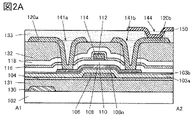
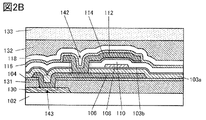
- FIGS. 2A and 2B show an example in which a part of the configuration is different from that of the above configuration example 1.
- the configurations shown in FIGS. 2A and 2B are mainly different in that the shape of the insulating layer 110 is different.
- the insulating layer 110 is provided so as to cover the upper surface of the insulating layer 103b, the upper surface and the side surface of the semiconductor layer 108.
- the insulating layer 110 is provided in contact with the upper surface of the low resistance region 108n as well as the channel forming region of the semiconductor layer 108.
- the low resistance region 108n can be formed by forming the insulating layer 110, the metal oxide layer 114, and the conductive layer 112, and then supplying impurities or the like through the insulating layer 110 with the conductive layer 112 as a mask. ..
- the above-mentioned impurity element can be supplied to the semiconductor layer 108 via the insulating layer 110 by plasma treatment, plasma ion doping method, ion implantation method, or the like.
- the covering property of the insulating layer 116 in the vicinity of the end portion of the conductive layer 112 can be improved, so that the reliability and the manufacturing yield can be improved.
- FIG. 3A The configuration shown in FIG. 3A is mainly different from the above configuration example 1 in that it has a conductive layer 121a and a conductive layer 121b.
- the conductive layer 120a is electrically connected to the low resistance region 108n via the conductive layer 121a. Further, the conductive layer 120b is electrically connected to the low resistance region 108n via the conductive layer 121b. Therefore, the conductive layer 121a and the conductive layer 121b can also be referred to as relay wiring, respectively.
- the conductive layer 121a and the conductive layer 121b are provided between the insulating layer 118 and the resin layer 132.
- the conductive layer 121a and the conductive layer 121b are electrically connected to the low resistance region 108n at the openings provided in the insulating layer 118 and the insulating layer 116, respectively.
- the conductive layer 120a and the conductive layer 120b are electrically connected to the conductive layer 121a and the conductive layer 121b, respectively, at the openings provided in the resin layer 132.
- the conductive layer 121a and the conductive layer 121b that function as relay wiring between the insulating layer 118 and the resin layer 132 in this way, it is not necessary to form a deep contact hole, so that the production yield can be increased. Can be done.
- the resin layer 132 containing a resin and the insulating layer 118 and the insulating layer 116 containing an inorganic insulating film are opened in a series of steps, not only the restrictions on the processing conditions become stricter but also the bottom of the opening is opened. Problems such as the disappearance of the positioned semiconductor layer 108 or the increase in the opening diameter may occur.
- FIG. 3A shows an example in which the opening provided in the resin layer 132 and the opening provided in the insulating layer 118 and the insulating layer 116 overlap each other at the connection portion between the conductive layer 120a and the conductive layer 121a. ing. Further, like the connection portion between the conductive layer 120b and the conductive layer 121b, the above two openings may be staggered so as not to be overlapped with each other.
- FIG. 3B is an example in which the conductive layer 121a and the conductive layer 121b are applied to the configuration exemplified in the above configuration example 2.
- the conductive layer 121a and the conductive layer 121b are electrically connected to the low resistance region 108n at the openings provided in the insulating layer 118, the insulating layer 116, and the insulating layer 110, respectively.
- the thin films (insulating film, semiconductor film, conductive film, etc.) constituting the semiconductor device include a sputtering method, a chemical vapor deposition (CVD) method, a vacuum vapor deposition method, and a pulsed laser deposition (PLD: Pulsed Laser Deposition).
- CVD chemical vapor deposition
- ALD Atomic Layer Deposition
- CVD method examples include a plasma chemical vapor deposition (PECVD: Plasma Enhanced CVD) method and a thermal CVD method.
- PECVD plasma chemical vapor deposition
- thermal CVD there is an organometallic chemical vapor deposition (MOCVD: Metalorganic CVD) method.
- the thin films (insulating film, semiconductor film, conductive film, etc.) that make up the semiconductor device are spin coated, dip, spray coated, inkjet, dispense, screen printing, offset printing, doctor knife, slit coat, roll coat, curtain coat. , Can be formed by a method such as knife coating.
- a thin film constituting a semiconductor device when processing a thin film constituting a semiconductor device, it can be processed by using a photolithography method or the like.
- the thin film may be processed by a nanoimprint method, a sandblast method, a lift-off method, or the like.
- an island-shaped thin film may be directly formed by a film forming method using a shielding mask such as a metal mask.
- photolithography methods There are typically the following two methods as photolithography methods.
- One is a method of forming a resist mask on a thin film to be processed, processing the thin film by etching or the like, and removing the resist mask.
- the other is a method in which a photosensitive thin film is formed, and then exposed and developed to process the thin film into a desired shape.
- the light used for exposure for example, i-line (wavelength 365 nm), g-line (wavelength 436 nm), h-line (wavelength 405 nm), or a mixture of these can be used.
- ultraviolet rays, KrF laser light, ArF laser light, or the like can also be used.
- the exposure may be performed by the immersion exposure technique.
- extreme ultraviolet (EUV: Extreme Ultra-violet) light or X-rays may be used as the light used for exposure.
- an electron beam can be used instead of the light used for exposure. It is preferable to use extreme ultraviolet light, X-rays or an electron beam because extremely fine processing is possible.
- extreme ultraviolet light, X-rays or an electron beam because extremely fine processing is possible.
- a dry etching method, a wet etching method, a sandblasting method, etc. can be used for etching the thin film.
- 4A to 8B show side-by-side cross sections in the channel length direction and the channel width direction at each stage of the manufacturing process of the semiconductor device exemplified in the configuration example 2.
- a conductive film is formed on the substrate 102 and processed by etching to form a conductive layer 130 that functions as wiring (FIG. 4A).
- the resin layer 131 to be formed later functions as a flattening film and has extremely high coverage, the conductive layer 130 does not have to be tapered. Further, since the conductive layer 130 can be made thicker, it is possible to reduce the wiring resistance of the wiring to which the conductive layer 130 is applied.
- the wiring resistance can be reduced.
- a conductive film containing copper As the conductive film to be the conductive layer 106, the wiring resistance can be reduced.
- the insulating layer 103a suppresses the diffusion of copper toward the semiconductor layer 108, so that a highly reliable transistor can be realized.
- the resin layer 131 is a mixture of the resin precursor and the solvent by, for example, spin coating, dipping, spray coating, inkjet, dispensing, screen printing, offset printing, doctor knife, slit coating, roll coating, curtain coating, knife coating and the like.
- the material is formed on the support substrate. After that, by performing a heat treatment, the material can be cured while removing the solvent and the like to form the resin layer 131 containing the organic resin.
- polyimide As the organic resin that can be used for the resin layer 131, polyimide can be typically used. Polyimide is preferable because it has excellent heat resistance. In addition, acrylic, epoxy, polyamide, polyimideamide, siloxane, benzocyclobutene resin, phenol resin and the like can be used.
- polyimide when polyimide is used, a resin precursor that forms an imide bond by dehydration can be used. Alternatively, a material containing soluble polyimide may be used.
- the organic resin used for the resin layer 131 either photosensitive or non-photosensitive resin may be used.
- the photosensitive polyimide is a material preferably used for a flattening film or the like of a display panel, a forming device and a material can be shared. Therefore, no new device, material, or the like is required to realize the configuration of one aspect of the present invention.
- a photosensitive resin material and subjecting it to exposure and development treatment for example, an opening can be formed or an unnecessary portion can be removed.
- optimizing the exposure method and the exposure conditions it is possible to form an uneven shape on the surface. For example, a multiple exposure technique, an exposure technique using a halftone mask or a gray tone mask, or the like may be used.
- the insulating layer 104 is formed on the resin layer 131 (FIG. 4C).
- the insulating layer 104 can be formed by using a PECVD method, an ALD method, a sputtering method, or the like.
- opening 143 a resist mask is formed on the insulating layer 104, and a part of the insulating layer 104 is removed by etching to form an opening in the insulating layer 104. Subsequently, using the insulating layer 104 as a hard mask, an opening reaching the conductive layer 130 is formed in a part of the resin layer 131 to form an opening 143 (FIG. 4D).
- the diameter of the opening 143 can be reduced.
- the resin layer 131 is preferably etched by dry etching. For example, it can be etched by an ashing process using plasma.
- the opening 143 may be formed by using the following method. First, a photosensitive material is used for the resin layer 131, and exposure and development are performed to form the resin layer 131 having an opening overlapping with the conductive layer 130. Subsequently, after the insulating layer 104 is formed into a film, the opening portion 143 can be formed by removing the portion overlapping the opening of the resin layer 131 by etching. In this method, the step of etching the thick resin layer 131 can be omitted.
- conductive layer 106 is formed by covering the insulating layer 104 and the opening 143, and this is processed by etching to form a conductive layer 106 that functions as a gate electrode (FIG. 4E).
- the wiring resistance can be reduced.
- the insulating layer 103a and the insulating layer 103b can be formed by using a PECVD method, an ALD method, a sputtering method, or the like.
- the insulating layer 103a and the insulating layer 103b are laminated and formed.
- the insulating layer 103a and the insulating layer 103b are preferably formed by the PECVD method.
- a process of supplying oxygen to the insulating layer 103b may be performed.
- plasma treatment or heat treatment in an oxygen atmosphere can be performed.
- oxygen may be supplied to the insulating layer 103b by a plasma ion doping method, an ion implantation method, or the like.
- the metal oxide film is preferably formed by a sputtering method using a metal oxide target.
- the metal oxide film is preferably a dense film with as few defects as possible. Further, the metal oxide film is preferably a high-purity film in which impurities such as hydrogen and water are reduced as much as possible. In particular, it is preferable to use a metal oxide film having crystallinity.
- oxygen gas and an inert gas for example, helium gas, argon gas, xenon gas, etc.
- oxygen flow rate ratio the ratio of oxygen gas to the entire film formation gas
- a high-quality transistor can be realized.
- the lower the oxygen flow rate ratio the lower the crystallinity of the metal oxide film, and the transistor can be made with an increased on-current.
- the substrate temperature may be room temperature or higher and 250 ° C. or lower, preferably room temperature or higher and 200 ° C. or lower, and more preferably the substrate temperature is room temperature or higher and 140 ° C. or lower.
- productivity is high and it is preferable.
- the crystallinity can be lowered by forming a metal oxide film at a substrate temperature of room temperature or in a state where the substrate is not intentionally heated.
- At least one of the treatments for desorbing water, hydrogen, organic substances, etc. adsorbed on the surface of the insulating layer 103b and the treatment for supplying oxygen into the insulating layer 103b before forming the metal oxide film can be performed at a temperature of 70 ° C. or higher and 200 ° C. or lower in a reduced pressure atmosphere.
- plasma treatment may be performed in an atmosphere containing oxygen.
- oxygen may be supplied to the insulating layer 103b by plasma treatment in an atmosphere containing an oxidizing gas such as nitrous oxide ( N2O).
- oxygen can be supplied while suitably removing organic substances on the surface of the insulating layer 103b. After such treatment, it is preferable to continuously form a metal oxide film without exposing the surface of the insulating layer 103b to the atmosphere.
- the metal oxide film to be formed first is formed, and then the surface thereof is continuously formed without being exposed to the atmosphere. It is preferable to form the following metal oxide film.
- either one or both of the wet etching method and the dry etching method may be used.
- a part of the insulating layer 103b that does not overlap with the semiconductor layer 108 may be etched and thinned.
- the insulating layer 103b may disappear by etching and the surface of the insulating layer 103a may be exposed.
- heat treatment after forming the metal oxide film or processing the metal oxide film into the semiconductor layer 108.
- heat treatment hydrogen or water contained in or adsorbed on the surface of the metal oxide film or the semiconductor layer 108 can be removed. Further, the heat treatment may improve the film quality of the metal oxide film or the semiconductor layer 108 (for example, reduction of defects, improvement of crystallinity, etc.).
- oxygen can be supplied from the insulating layer 103b to the metal oxide film or the semiconductor layer 108 by heat treatment. At this time, it is more preferable to perform heat treatment before processing the semiconductor layer 108.
- the temperature of the heat treatment can be typically 150 ° C. or higher and lower than the strain point of the substrate, 200 ° C. or higher and 500 ° C. or lower, 250 ° C. or higher and 450 ° C. or lower, or 300 ° C. or higher and 450 ° C. or lower.
- the heat treatment can be performed in an atmosphere containing noble gas or nitrogen. Alternatively, after heating in the atmosphere, heating may be performed in an atmosphere containing oxygen. Alternatively, it may be heated in a dry air atmosphere. It is preferable that the atmosphere of the heat treatment does not contain hydrogen, water or the like as much as possible.
- an electric furnace, an RTA (Rapid Thermal Anneal) device, or the like can be used. By using the RTA device, the heat treatment time can be shortened.
- the heat treatment is unnecessary, it may not be performed. Further, the heat treatment is not performed here, and may be combined with the heat treatment performed in a later step. In addition, it may be possible to combine the heat treatment with a treatment under a high temperature (for example, a film forming step) in a later step.
- a high temperature for example, a film forming step
- Insulation Layer 110 [Formation of Insulation Layer 110] Subsequently, the insulating layer 103b and the semiconductor layer 108 are covered to form the insulating layer 110.
- the insulating layer 110 is preferably formed by the PECVD method.
- the plasma treatment it is preferable to perform plasma treatment on the surface of the semiconductor layer 108 before forming the insulating layer 110.
- impurities such as water adsorbed on the surface of the semiconductor layer 108 can be reduced. Therefore, impurities at the interface between the semiconductor layer 108 and the insulating layer 110 can be reduced, so that a highly reliable transistor can be realized.
- the plasma treatment can be performed in an atmosphere such as oxygen, ozone, nitrogen, nitrous oxide, or argon. Further, it is preferable that the plasma treatment and the film formation of the insulating layer 110 are continuously performed without being exposed to the atmosphere.
- heat treatment it is preferable to perform heat treatment after forming the insulating layer 110.
- heat treatment hydrogen or water contained in the insulating layer 110 or adsorbed on the surface can be removed.
- defects in the insulating layer 110 can be reduced.
- the heat treatment is unnecessary, it may not be performed. Further, the heat treatment is not performed here, and may be combined with the heat treatment performed in a later step. In addition, it may be possible to combine the heat treatment with a treatment under a high temperature (for example, a film forming step) in a later step.
- a high temperature for example, a film forming step
- the metal oxide film 114f is preferably formed in an atmosphere containing oxygen, for example. In particular, it is preferably formed by the sputtering method in an atmosphere containing oxygen. As a result, oxygen can be supplied to the insulating layer 110 when the metal oxide film 114f is formed. Oxygen may be supplied to the semiconductor layer 108 at the time of forming the metal oxide film 114f.
- the metal oxide film 114f is formed by a sputtering method using an oxide target containing a metal oxide similar to that of the semiconductor layer 108, the description of the semiconductor layer 108 can be incorporated.
- the metal oxide film may be formed by a reactive sputtering method using oxygen as the film forming gas and using a metal target.
- a metal target for example, an aluminum oxide film can be formed.
- the oxygen supplied into the layer 110 can be increased.
- the oxygen flow rate ratio or oxygen partial pressure is, for example, 50% or more and 100% or less, preferably 65% or more and 100% or less, more preferably 80% or more and 100% or less, and further preferably 90% or more and 100% or less.
- it is preferable that the oxygen flow rate ratio is 100% and the oxygen partial pressure in the film forming chamber is as close as possible to 100%.
- heat treatment oxygen contained in the insulating layer 110 can be supplied to the semiconductor layer 108.
- oxygen can be prevented from being desorbed from the insulating layer 110 to the outside, and a large amount of oxygen can be supplied to the semiconductor layer 108.
- oxygen deficiency in the semiconductor layer 108 can be reduced, and a highly reliable transistor can be realized.
- the heat treatment is unnecessary, it may not be performed. Further, the heat treatment is not performed here, and may be combined with the heat treatment performed in a later step. In addition, it may be possible to combine the heat treatment with a treatment under a high temperature (for example, a film forming step) in a later step.
- a high temperature for example, a film forming step
- the metal oxide film 114f may be removed after the film formation of the metal oxide film 114f or after the heat treatment.
- opening 142 [Formation of opening 142] Subsequently, by etching a part of the metal oxide film 114f, the insulating layer 110, the insulating layer 103b, and the insulating layer 103a, an opening 142 reaching the conductive layer 106 is formed (FIG. 5C). Thereby, the conductive layer 106 and the conductive layer 112 to be formed later can be electrically connected to each other through the opening 142.
- the conductive film 112f it is preferable to use a metal or alloy material having low resistance. Further, as the conductive film 112f, it is preferable to use a material that does not easily release hydrogen and that does not easily diffuse hydrogen. Further, it is preferable to use a material that is hard to oxidize as the conductive film 112f.
- the conductive film 112f is preferably formed by a sputtering method using a sputtering target containing a metal or an alloy.
- the conductive film 112f it is preferable to use a laminated film in which a conductive film that is difficult to oxidize and hydrogen is not easily diffused and a conductive film having low resistance are laminated.
- the conductive layer 112 and the metal oxide layer 114 are formed by etching a part of the conductive film 112f and the metal oxide film 114f. It is preferable that the conductive film 112f and the metal oxide film 114f are each processed using the same resist mask. Alternatively, the metal oxide film 114f may be etched by using the etched conductive layer 112 as a hard mask.
- the conductive layer 112 and the metal oxide layer 114 having substantially the same top surface shape can be formed.
- the semiconductor layer 108 and the insulating layer are formed when the conductive film 112f or the like is etched. It is possible to prevent 103b and the like from being etched and thinned.
- a process of supplying (also referred to as addition or injection) of the impurity element 140 to the semiconductor layer 108 via the insulating layer 110 is performed (FIG. 6A).
- the impurity element 140 is supplied in consideration of the material and thickness of the conductive layer 112 or the like as a mask so that the impurity element 140 is not supplied to the region overlapping the conductive layer 112 of the semiconductor layer 108 as much as possible. It is preferable to determine the conditions. As a result, it is possible to form a channel forming region in which the impurity concentration is sufficiently reduced in the region overlapping the conductive layer 112 of the semiconductor layer 108.
- a plasma ion doping method or an ion implantation method can be preferably used.
- the concentration profile in the depth direction can be controlled with high accuracy by the acceleration voltage of ions, the dose amount, and the like.
- Productivity can be increased by using the plasma ion doping method.
- the ion implantation method using mass separation the purity of the supplied impurity element can be increased.
- the interface between the semiconductor layer 108 and the insulating layer 110, the portion of the semiconductor layer 108 near the interface, or the portion of the insulating layer 110 near the interface has the highest concentration.
- the impurity element 140 having an optimum concentration can be supplied to both the semiconductor layer 108 and the insulating layer 110 by one treatment.
- Examples of the impurity element 140 include hydrogen, boron, carbon, nitrogen, fluorine, phosphorus, sulfur, arsenic, aluminum, magnesium, silicon, and rare gas.
- Typical examples of the noble gas include helium, neon, argon, krypton, xenon and the like. In particular, it is preferable to use boron, phosphorus, aluminum, magnesium, or silicon.
- a gas containing the impurity element can be used as the raw material gas for the impurity element 140.
- a gas containing the impurity element can be used.
- B 2 H 6 gas, BF 3 gas, or the like can be typically used.
- PH 3 gas can be typically used.
- a mixed gas obtained by diluting these raw material gases with a rare gas may be used.
- raw material gas CH 4 , N 2 , NH 3 , AlH 3 , AlCl 3 , SiH 4 , Si 2 H 6 , F 2 , HF, H 2 , (C 5 H 5 ) 2 Mg, rare gas, etc.
- the ion source is not limited to gas, and a solid or liquid may be heated and vaporized.
- the addition of the impurity element 140 can be controlled by setting conditions such as an acceleration voltage or a dose amount in consideration of the composition, density, thickness and the like of the insulating layer 110 and the semiconductor layer 108.
- the dose amount is, for example, 1 ⁇ 10 13 ions / cm 2 or more and 1 ⁇ 10 17 ions / cm 2 or less, preferably 1 ⁇ 10 14 It can be in the range of ions / cm 2 or more and 5 ⁇ 10 16 ions / cm 2 or less, more preferably 1 ⁇ 10 15 ions / cm 2 or more and 3 ⁇ 10 16 ions / cm 2 or less.
- the method of supplying the impurity element 140 is not limited to this, and for example, a treatment using heat diffusion by heating, a plasma treatment, or the like may be used.
- the impurity element can be added by generating plasma in a gas atmosphere containing the impurity element to be added and performing the plasma treatment.
- a dry etching device, an ashing device, a plasma CVD device, a high-density plasma CVD device, or the like can be used as the device for generating the plasma.
- the impurity element 140 can be supplied to the semiconductor layer 108 via the insulating layer 110. Therefore, even when the semiconductor layer 108 has crystallinity, the damage to the semiconductor layer 108 when the impurity element 140 is supplied can be reduced, and the crystallinity can be suppressed from being impaired. Therefore, it is suitable when the electric resistance increases due to the decrease in crystallinity.
- Insulating Layer 116 and Insulating Layer 118 [Formation of Insulating Layer 116 and Insulating Layer 118] Subsequently, the insulating layer 110, the metal oxide layer 114, and the conductive layer 112 are covered to form the insulating layer 116 and the insulating layer 118 (FIG. 6B).
- the film formation temperature of the insulating layer 116 and the insulating layer 118 may be determined in consideration of these factors.
- the film formation temperature of the insulating layer 116 and the insulating layer 118 is preferably, for example, 150 ° C. or higher and 400 ° C. or lower, preferably 180 ° C. or higher and 360 ° C. or lower, and more preferably 200 ° C. or higher and 250 ° C. or lower.
- the low resistance region 108n may be made more stable and have low resistance.
- the impurity element 140 can be appropriately diffused and locally homogenized, and a low resistance region 108n having an ideal impurity element concentration gradient can be formed. If the temperature of the heat treatment is too high (for example, 500 ° C. or higher), the impurity element 140 may diffuse into the channel forming region, which may lead to deterioration of the electrical characteristics and reliability of the transistor.
- the heat treatment is unnecessary, it may not be performed. Further, the heat treatment is not performed here, and may be combined with the heat treatment performed in a later step. Further, when there is a treatment under high temperature (for example, a film forming step) in a later step, it may be possible to combine the heat treatment.
- the description of the resin layer 131 can be referred to.
- a photosensitive material is used, and the resin layer 132 having an opening is formed by exposure and development.
- the resin layer 132 is used as an etching mask, and the portions of the insulating layer 118, the insulating layer 116, and the insulating layer 110 located in the opening of the resin layer 132 are etched.
- the opening 141a and the opening 141b may be formed by using the following method. First, before forming the resin layer 132, a resist mask is formed on the insulating layer 118, and openings are formed in advance in the insulating layer 118, the insulating layer 116, and the insulating layer 110. Subsequently, the resin layer 132 having an opening is formed by performing exposure and development using a photosensitive material. Thereby, the opening 141a and the opening 141b can be formed.
- a semiconductor device including a transistor can be manufactured.
- the description of the resin layer 131 and the resin layer 132 can be referred to.
- conductive layer 150 [Formation of conductive layer 150] Subsequently, a conductive film is formed on the resin layer 133 so as to cover the opening 144, and the conductive film is processed into a desired shape to form the conductive layer 150 (FIG. 8B).
- ⁇ substrate ⁇ There are no major restrictions on the material of the substrate 102, but at least it must have heat resistance sufficient to withstand the subsequent heat treatment.
- a single crystal semiconductor substrate made of silicon or silicon carbide, a polycrystalline semiconductor substrate, a compound semiconductor substrate such as silicon germanium, an SOI substrate, a glass substrate, a ceramic substrate, a quartz substrate, a sapphire substrate, or the like is used as the substrate 102. May be good. Further, those in which semiconductor elements are provided on these substrates may be used as the substrate 102.
- a flexible substrate may be used as the substrate 102, and the semiconductor device may be formed directly on the flexible substrate.
- a release layer may be provided between the substrate 102 and the semiconductor device. The release layer can be used for separating the semiconductor device from the substrate 102 and reprinting it on another substrate after the semiconductor device is partially or completely completed on the release layer. At that time, the semiconductor device can be reprinted on a substrate having inferior heat resistance or a flexible substrate.
- the conductive layer 112, the conductive layer 106, the conductive layer 120a, the conductive layer 120b, the conductive layer 121a, the conductive layer 121b, the conductive layer 130, the conductive layer 150 and the like are made of chromium, copper, aluminum, gold, silver, zinc, molybdenum and tantalum. , Titanium, tungsten, manganese, nickel, iron, a metal element selected from cobalt, an alloy containing the above-mentioned metal element as a component, an alloy obtained by combining the above-mentioned metal elements, and the like.
- the conductive layer includes In-Sn oxide, In-W oxide, In-W-Zn oxide, In-Ti oxide, In-Ti-Sn oxide, In-Zn oxide, In-Sn.
- An oxide conductor such as ⁇ Si oxide or In—Ga—Zn oxide or a metal oxide film can also be applied.
- the semiconductor layer 108 is an In—M—Zn oxide
- the atomic number ratio of the semiconductor layer 108 to be formed includes a variation of plus or minus 40% of the atomic number ratio of the metal element contained in the sputtering target.
- the semiconductor layer 108 has an energy gap of 2 eV or more, preferably 2.5 eV or more. As described above, by using a metal oxide having a wider energy gap than silicon, the off-current of the transistor can be reduced.
- the semiconductor layer 108 preferably has a non-single crystal structure.
- the non-single crystal structure includes, for example, a CAAC structure, a polycrystalline structure, a microcrystal structure, or an amorphous structure described later.
- the amorphous structure has the highest defect level density
- the CAAC structure has the lowest defect level density.
- CAAC c-axis aligned critical
- the CAAC structure is one of crystal structures such as a thin film having a plurality of nanocrystals (crystal regions having a maximum diameter of less than 10 nm), and each nanocrystal has a c-axis oriented in a specific direction and an a-axis.
- the b-axis is a crystal structure having no orientation and having a feature that nanocrystals are continuously connected without forming grain boundaries.
- the thin film having a CAAC structure has a feature that the c-axis of each nanocrystal is easily oriented in the thickness direction of the thin film, the normal direction of the surface to be formed, or the normal direction of the surface of the thin film.
- CAAC-OS Oxide Semiconductor
- CAAC-OS Oxide Semiconductor
- CAAC-OS since a clear crystal grain boundary cannot be confirmed, it can be said that the decrease in electron mobility due to the crystal grain boundary is unlikely to occur. Further, since the crystallinity of the oxide semiconductor may be deteriorated due to the mixing of impurities, the generation of defects, etc., CAAC-OS can be said to be an oxide semiconductor having few impurities and defects (oxygen deficiency, etc.). Therefore, the oxide semiconductor having CAAC-OS has stable physical properties. Therefore, the oxide semiconductor having CAAC-OS is resistant to heat and has high reliability.
- crystallography it is common to take a unit cell with a specific axis as the c axis for the three axes (crystal axis) of the a-axis, b-axis, and c-axis that compose the unit cell. ..
- a crystal having a layered structure it is common that two axes parallel to the plane direction of the layer are the a-axis and the b-axis, and the axes intersecting the layers are the c-axis.
- a typical example of a crystal having such a layered structure is graphite classified into a hexagonal system.
- the a-axis and b-axis of the unit cell are parallel to the cleavage plane, and the c-axis is orthogonal to the cleavage plane. do.
- the crystal of InGaZnO 4 having a layered structure of YbFe 2 O 4 type can be classified into a hexagonal system, and the a-axis and b-axis of the unit cell are parallel to the plane direction of the layer and the c-axis. Is orthogonal to the layer (ie, a-axis and b-axis).
- the crystal part may not be clearly confirmed in the observation image by TEM.
- the crystal part contained in the microcrystalline oxide semiconductor film often has a size of 1 nm or more and 100 nm or less, or 1 nm or more and 10 nm or less.
- an oxide semiconductor film having nanocrystals nc: nanocrystals
- nc-OS nanocrystalline Oxide Semiconductor
- the crystal grain boundaries may not be clearly confirmed in the observation image by TEM.
- the nc-OS film has periodicity in the atomic arrangement in a minute region (for example, a region of 1 nm or more and 10 nm or less, particularly a region of 1 nm or more and 3 nm or less).
- the nc-OS film does not show regularity in crystal orientation between different crystal portions. Therefore, no orientation is observed in the entire film. Therefore, the nc-OS film may be indistinguishable from the amorphous oxide semiconductor film depending on the analysis method. For example, when structural analysis is performed on an nc-OS film using an XRD apparatus using an X-ray having a diameter larger than that of the crystal portion, a peak indicating a crystal plane is not detected in the analysis by the out-of-plane method.
- electron beam diffraction also referred to as limited field electron diffraction
- a diffraction pattern such as a halo pattern is performed. Is observed.
- electron diffraction also referred to as nanobeam electron diffraction
- a probe diameter for example, 1 nm or more and 30 nm or less
- the nc-OS film has a lower defect level density than the amorphous oxide semiconductor film.
- the nc-OS film there is no regularity in the crystal orientation between different crystal portions. Therefore, the nc-OS film has a higher defect level density than the CAAC-OS film. Therefore, the nc-OS film may have a higher carrier density and higher electron mobility than the CAAC-OS film. Therefore, a transistor using an nc-OS film may exhibit high field effect mobility.
- the nc-OS film can be formed by reducing the oxygen flow rate ratio at the time of film formation as compared with the CAAC-OS film. Further, the nc-OS film can also be formed by lowering the substrate temperature at the time of film formation as compared with the CAAC-OS film. For example, the nc-OS film can be formed even when the substrate temperature is relatively low (for example, a temperature of 130 ° C. or lower) or the substrate is not heated, so that a large glass substrate or a resin substrate can be formed. It is suitable for use and can increase productivity.
- a metal oxide An example of the crystal structure of a metal oxide will be described.
- the substance tends to have a crystal structure of either an nc (nano crystal) structure or a CAAC structure, or a structure in which these are mixed.
- the metal oxide formed with the substrate temperature at room temperature (RT) tends to have an nc crystal structure.
- the room temperature (RT) referred to here includes a temperature when the substrate is not intentionally heated.
- CAAC c-axis aligned crystal
- CAC Cloud-Indexed Composite
- the CAC-OS or CAC-metal oxide has a conductive function in a part of the material and an insulating function in a part of the material, and has a function as a semiconductor in the whole material.
- the conductive function is the function of allowing electrons (or holes) to be carriers to flow
- the insulating function is the function of allowing electrons (or holes) to be carriers. It is a function that does not shed.
- CAC-OS or CAC-metal oxide has a conductive region and an insulating region.
- the conductive region has the above-mentioned conductive function
- the insulating region has the above-mentioned insulating function.
- the conductive region and the insulating region may be separated at the nanoparticle level. Further, the conductive region and the insulating region may be unevenly distributed in the material. In addition, the conductive region may be observed with the periphery blurred and connected in a cloud shape.
- CAC-OS or CAC-metal oxide when the conductive region and the insulating region are dispersed in the material in a size of 0.5 nm or more and 10 nm or less, preferably 0.5 nm or more and 3 nm or less, respectively. There is.
- CAC-OS or CAC-metal oxide is composed of components having different band gaps.
- CAC-OS or CAC-metal oxide is composed of a component having a wide gap due to an insulating region and a component having a narrow gap due to a conductive region.
- the carrier when the carrier is flown, the carrier mainly flows in the component having a narrow gap.
- the component having a narrow gap acts complementarily to the component having a wide gap, and the carrier flows to the component having a wide gap in conjunction with the component having a narrow gap. Therefore, when the CAC-OS or CAC-metal oxide is used in the channel forming region of the transistor, a high current driving force, that is, a large on-current and a high field effect mobility can be obtained in the ON state of the transistor.
- CAC-OS or CAC-metal oxide can also be referred to as a matrix composite material (matrix composite) or a metal matrix composite material (metal matrix composite).
- FIG. 9A shows a schematic top view of the display device 10 illustrated below.
- the display device 10 includes a pixel unit 11, a circuit 12, a circuit 13, a terminal unit 15a, a terminal unit 15b, a wiring 16a, a wiring 16b, and a wiring 16c. Further, FIG. 9A shows an example in which the IC 17 is mounted on the display device 10.
- the pixel unit 11 has a plurality of pixels and has a function of displaying an image.
- the circuit 12 and the IC 17 have a function of outputting a signal for driving the pixel to each pixel in the pixel unit 11.
- the circuit 12 is a circuit that functions as a gate drive circuit.
- the IC 17 is a circuit that functions as a source drive circuit.
- FIG. 9A shows an example in which two circuits 12 are provided with the pixel portion 11 interposed therebetween, and six ICs 17 are mounted. An IC that functions as a gate drive circuit may be mounted, and the circuit 12 may not be provided. Further, a source drive circuit may be provided and the IC 17 may not be mounted.
- a form in which an integrated circuit such as an IC or a connector such as an FPC (Flexible Printed Circuit) is mounted can also be called a display module. Further, a form in which a connector or an integrated circuit is not mounted can also be called a display panel.
- FPC Flexible Printed Circuit
- the circuit 13 is a circuit (for example, a demultiplexer circuit) having a function of distributing one of the signals input from the IC 17 to two or more wires.
- a circuit for example, a demultiplexer circuit
- the number of signals output by the IC 17 can be reduced, and the number of terminals of the IC 17 can be reduced. Or the number of parts can be reduced.
- the circuit 13 may not be provided if it is unnecessary.
- a plurality of terminals are provided in the terminal portion 15a and the terminal portion 15b, and a connector such as an FPC or an integrated circuit such as another IC can be connected.
- Each terminal of the terminal portion 15a is electrically connected to the circuit 12 via one of the plurality of wirings 16a.
- Each terminal of the terminal portion 15b is electrically connected to the IC 17 via one of the plurality of wirings 16b.
- the plurality of output terminals of the IC 17 are electrically connected to the circuit 13 via one of the plurality of wirings 16c, respectively.
- FIG. 9B is a schematic top view showing an example of a method of arranging pixel electrodes in the pixel portion 11.
- the pixel unit 11 has a plurality of pixel units 20.
- FIG. 9B shows four pixel units 20.
- the pixel unit 20 includes pixels 21a and pixels 21b.
- the pixel 21a has a pixel electrode 31a, a pixel electrode 32a, and a pixel electrode 33a.
- the pixel 21b has a pixel electrode 31b, a pixel electrode 32b, and a pixel electrode 33b.
- Each pixel electrode functions as an electrode of a display element described later.
- the display area 22 of one sub-pixel is located inside the pixel electrode of the sub-pixel.
- the six pixel electrodes of the pixel unit 20 are arranged in a matrix of two in the vertical direction and three in the horizontal direction.
- the pixel electrode 31a, the pixel electrode 32a, and the pixel electrode 33a can be electrodes of display elements exhibiting different colors.
- the pixel electrode 31b can be a pixel electrode 31a
- the pixel electrode 32b can be a pixel electrode 32a
- the pixel electrode 33b can be a pixel electrode 33a as electrodes of display elements having the same color.
- the sizes of the three types of pixel electrodes are specified here as being the same, they may have different sizes. Alternatively, the size of the display area 22 on each pixel electrode may be different.
- the pixel electrode 31a is designated as an electrode of a display element exhibiting a red color (R) and is designated by an R.
- the pixel electrode 32a is designated by G as an electrode of a display element exhibiting green color (G)
- the pixel electrode 33a is designated by B as an electrode of a display element exhibiting blue color (B).
- the pixel arrangement shown in FIG. 9B and the like is an example, and is not limited to this. Further, R, G, and B can exchange these with each other. Further, a pixel array in which the pixel array shown in FIG. 9B or the like is flipped horizontally or vertically may be used.
- the method of arranging the display elements is not limited to the above, and may be, for example, a so-called stripe arrangement in which three rectangular display elements are arranged in one square. Alternatively, it may be a so-called delta array in which any of the three display elements is arranged at the vertices of a lattice in which triangles of the same shape are spread.
- FIG. 9C shows an example of a circuit diagram of the pixel unit 20.
- Wiring 51a and 51b, wiring 52a to 52d, and wiring 53a to 53c are connected to the pixel unit 20.
- FIG. 9C shows an example in which four wires (wiring 52a, etc.) that function as signal lines are connected to one pixel unit 20.
- the pixel 21a has a sub-pixel 71a, a sub-pixel 72a, and a sub-pixel 73a.
- the pixel 21b has a sub-pixel 71b, a sub-pixel 72b, and a sub-pixel 73b.
- Each sub-pixel has a pixel circuit (pixel circuit 41a, pixel circuit 41b, pixel circuit 42a, pixel circuit 42b, pixel circuit 43a or pixel circuit 43b) and a display element 60.
- the sub-pixel 71a has a pixel circuit 41a and a display element 60.
- a light emitting element such as an organic EL element is used as the display element 60 is shown.
- each pixel circuit has a transistor 61, a transistor 62, and a capacitive element 63.
- the gate is electrically connected to the wiring 51a
- one of the source or the drain is electrically connected to the wiring 52a
- the other of the source or the drain is the gate of the transistor 62 and the capacitive element. It is electrically connected to one of the electrodes of 63.
- one of the source and the drain is electrically connected to one electrode of the display element 60
- the other of the source and the drain is electrically connected to the other electrode of the capacitive element 63 and the wiring 53a.
- the other electrode of the display element 60 is electrically connected to the wiring to which the potential V1 is given.
- the wiring connected to the gate of the transistor 61, the wiring connected to one of the source or drain of the transistor 61, and the wiring connected to the other electrode of the capacitive element 63 As for the other pixel circuits, as shown in FIG. 9C, the wiring connected to the gate of the transistor 61, the wiring connected to one of the source or drain of the transistor 61, and the wiring connected to the other electrode of the capacitive element 63. It has the same configuration as the pixel circuit 41a except that it is different.
- the transistor 61 has a function as a selection transistor. Further, the transistor 62 is connected in series with the display element 60 and has a function of controlling the current flowing through the display element 60. In FIG. 9C, it can be said that the transistor 61 that functions as a selection transistor and one electrode (pixel electrode) of the display element 60 are electrically connected via the transistor 62. Further, the capacitive element 63 has a function of holding the potential of the node to which the gate of the transistor 62 is connected. If the leak current in the off state of the transistor 61, the leak current through the gate of the transistor 62, and the like are extremely small, the capacitive element 63 may not be intentionally provided.
- the transistor 62 has a first gate and a second gate, which are electrically connected to each other, respectively. With the configuration having two gates in this way, the current that can be passed through the transistor 62 can be increased. Particularly in a high-definition display device, the current can be increased without increasing the size of the transistor 62, particularly the channel width, which is preferable.
- the electrode electrically connected to the transistor 62 corresponds to the pixel electrode (for example, the pixel electrode 31a or the like).
- FIG. 9C shows a configuration in which the electrode electrically connected to the transistor 62 of the display element 60 is used as a cathode and the electrode on the opposite side is used as an anode.
- the transistor 62 is an n-channel type transistor. That is, when the transistor 62 is in the ON state, the potential given by the wiring 53a becomes the source potential, so that the current flowing through the transistor 62 is constant regardless of the variation in the electrical resistance of the display element 60 and the variation in the electrical resistance. be able to.
- the electrode on the transistor 62 side of the display element 60 may be used as an anode, and the electrode on the opposite side may be used as a cathode.
- a fixed potential lower than the potential given to the wiring 53a or the like can be used for the potential V1 given to the other electrode of the display element 60.
- a potential common to the potential used for other circuits such as a common potential or a ground potential, for the potential V1 because the circuit configuration can be simplified.
- a p-channel type transistor may be used.
- FIGS. 10A and 10B show an example of the layout of one sub-pixel.
- an example before forming the pixel electrode is shown.
- the wiring 52 and the like in FIG. 10A are shown by broken lines.
- the sub-pixel shown in FIG. 10A has a transistor 61, a transistor 62, and a capacitive element 63.
- the transistor 62 is a transistor having two gates sandwiching the semiconductor layer.
- the transistor exemplified in the first embodiment can be applied to the transistor 61 and the transistor 62.
- the same hatching pattern is attached to a pattern formed by processing the same conductive film.
- the wiring 51 is formed by the conductive layer (conductive layer 130) located at the lowermost side.
- a relay wiring, one gate of the transistor 62, and the like are formed by the conductive layer (conductive layer 106a, conductive layer 106b, etc.) formed after this.
- the conductive layer (conductive layer 112a, conductive layer 112b, etc.) formed after this forms the gate of the transistor 61, the other gate of the transistor 62, and the like.
- the wiring 52, the wiring 53, the relay wiring, and the like are formed by the conductive layer (conductive layer 120a, conductive layer 120b, conductive layer 120c, etc.) formed after this.
- a part of the wiring 53 functions as the other electrode of the capacitive element 63.
- the conductive layer 120c functions as a relay wiring for connecting the transistor 62 and the pixel electrode 31 and the like.
- the transistor 61 has a semiconductor layer 108a
- the transistor 62 has a semiconductor layer 108b.
- FIG. 10C shows an example of the layout of the pixel unit 20 using the sub-pixels exemplified in FIG. 10A.
- each pixel electrode and the display area 22 are also clearly shown.
- the display area 22 of the three sub-pixels electrically connected to the wiring 51a and the display area 22 of the three sub-pixels electrically connected to the wiring 51b are half the arrangement pitch in the extending direction of the wiring 51a. It may be arranged so as to deviate from each other. This makes it possible to realize a so-called delta array.
- the display device exemplified in this embodiment can realize an extremely high-definition display device. Further, it is possible to provide a display device having improved display quality. Further, it is possible to provide a display device having improved viewing angle characteristics. Further, it is possible to provide a display device having an increased aperture ratio.
- FIG. 11 shows a schematic cross-sectional view of the display panel 700.
- FIG. 11 shows a cross section including a pixel unit 702, a gate driver circuit unit 706, and an FPC terminal unit 708.
- the pixel unit 702 includes a transistor 750, a transistor 754, and a capacitive element 790.
- the gate driver circuit unit 706 has a transistor 752.
- the transistor exemplified in the first embodiment can be applied to the transistor 750, the transistor 752, and the transistor 754.
- the transistor 750, the transistor 752, and the transistor 754 are transistors in which an oxide semiconductor is applied to the semiconductor layer on which a channel is formed. Not limited to this, a transistor using silicon (amorphous silicon, polycrystalline silicon, or single crystal silicon), an organic semiconductor, or the like can be applied to the semiconductor layer.
- the transistor used in this embodiment has an oxide semiconductor film that is highly purified and suppresses the formation of oxygen deficiency.
- the transistor can significantly reduce the off current. Therefore, in the pixel to which such a transistor is applied, the holding time of an electric signal such as an image signal can be lengthened, and the writing interval of the image signal or the like can be set to be long. Therefore, the frequency of refresh operations can be reduced, and power consumption can be reduced.
- the transistor used in this embodiment can be driven at high speed because a relatively high field effect mobility can be obtained.
- a transistor capable of high-speed drive for the display panel it is possible to form the switching transistor of the pixel portion and the driver transistor used for the drive circuit portion on the same substrate. That is, it is possible to configure a configuration in which a drive circuit formed of a silicon wafer or the like is not applied, and it is possible to reduce the number of parts of the display device. Further, even in the pixel portion, by using a transistor capable of high-speed driving, it is possible to provide a high-quality image.
- the capacitive element 790 has a lower electrode formed by processing the same film as the first gate electrode of the transistor 750 and an upper electrode formed by processing the same metal oxide film as the semiconductor layer. Have.
- the upper electrode has a low resistance as in the source region and drain region of the transistor 750. Further, a part of an insulating film that functions as a first gate insulating layer of the transistor 750 is provided between the lower electrode and the upper electrode. That is, the capacitive element 790 has a laminated structure in which an insulating film functioning as a dielectric film is sandwiched between a pair of electrodes. Further, wiring obtained by processing the same film as the source electrode and drain electrode of the transistor 750 is connected to the upper electrode.
- the display panel 700 has a support substrate 745 and a support substrate 740.
- a flexible substrate such as a glass substrate or a plastic substrate can be used.
- the transistor 750, the transistor 752, the transistor 754, the capacitive element 790, and the like are provided on the insulating layer 744.
- the support substrate 745 and the insulating layer 744 are bonded to each other by the adhesive layer 742.
- the conductive layer 720 is provided on the insulating layer 744.
- the resin layer 722 is provided so as to cover the insulating layer 744 and the conductive layer 720.
- the insulating layer 723 is provided so as to cover the resin layer 722.
- the transistor 750, the transistor 752, the transistor 754, the capacitive element 790, and the like are provided on the insulating layer 723.
- the transistor 750, the transistor 752, and the transistor 754 have a conductive layer 791 that functions as a first gate electrode, an insulating layer 792 that functions as a first gate insulating layer, a semiconductor layer 793, and an insulation that functions as a second gate insulating layer, respectively. It has a layer 794, a conductive layer 795 that functions as a second gate electrode, and the like. Further, an insulating layer 726 is provided so as to cover the transistor 750, the transistor 752, and the transistor 754.
- a resin layer 724 is provided on the insulating layer 726, and a conductive layer 725 or the like is provided on the resin layer 724.
- the conductive layer 721 formed by processing the same conductive film as the conductive layer 791 is electrically connected to the conductive layer 720 at the openings provided in the insulating layer 723 and the resin layer 722.
- a part of the conductive layer 720 functions as a gate wire.
- a part of the conductive layer 725 functions as a source line.
- a part of the conductive layer 720 and a part of the conductive layer 725 are overlapped with each other via at least the resin layer 722 and the resin layer 724.
- an insulating layer 770 that functions as a flattening film is provided on the transistor 750, the transistor 752, the transistor 754, and the capacitive element 790.
- the transistor 750 and the transistor 754 of the pixel unit 702 and the transistor 752 of the gate driver circuit unit 706 may use transistors having different structures from each other. For example, a top gate type transistor may be applied to one of them, and a bottom gate type transistor may be applied to any of the other.
- the FPC terminal portion 708 has a wiring 760, an anisotropic conductive film 780, and an FPC 716, part of which functions as a connection electrode.
- the wiring 760 is electrically connected to the terminal of the FPC 716 via the anisotropic conductive film 780.
- the wiring 760 is formed of the same conductive film as the source electrode and the drain electrode of the transistor 750 and the like.
- the display panel 700 has a light emitting element 782, a colored layer 736, a light shielding layer 738, and the like.
- the light emitting element 782 has a conductive layer 772, an EL layer 786, and a conductive layer 788.
- the conductive layer 772 is electrically connected to the source electrode or drain electrode of the transistor 750.
- the conductive layer 772 is provided on the insulating layer 770 and functions as a pixel electrode. Further, an insulating layer 730 is provided so as to cover the end portion of the conductive layer 772, and an EL layer 786 and a conductive layer 788 are laminated on the insulating layer 730 and the conductive layer 772.
- the light emitting element 782 is a top emission type light emitting element that emits light to the side opposite to the surface to be formed (support substrate 740 side).
- the EL layer 786 has an organic compound or an inorganic compound such as a quantum dot.
- the EL layer 786 contains a light emitting material that exhibits white light when an electric current flows.
- a fluorescent material As the light emitting material, a fluorescent material, a phosphorescent material, a Thermally activated delayed fluorescent (TADF) material, an inorganic compound (quantum dot material, etc.) and the like can be used.
- TADF Thermally activated delayed fluorescent
- quantum dot material an inorganic compound
- examples of materials that can be used for quantum dots include colloidal quantum dot materials, alloy-type quantum dot materials, core-shell type quantum dot materials, and core-type quantum dot materials.
- the light-shielding layer 738 and the colored layer 736 are provided on one surface of the insulating layer 746.
- the colored layer 736 is provided at a position overlapping with the light emitting element 782.
- the light-shielding layer 738 is provided in the pixel portion 702 in a region that does not overlap with the light-emitting element 782.
- the light-shielding layer 738 may be provided so as to be overlapped with the gate driver circuit unit 706 or the like.
- the support substrate 740 is bonded to the other surface of the insulating layer 746 by an adhesive layer 747. Further, the support substrate 740 and the support substrate 745 are bonded to each other by the sealing layer 732.
- the EL layer 786 of the light emitting element 782 a light emitting material exhibiting white light emission is applied.
- the white light emitted by the light emitting element 782 is colored by the colored layer 736 and emitted to the outside.
- the EL layer 786 is provided over pixels exhibiting different colors.
- a conductive film having transparency and reflectivity may be used as the conductive layer 788.
- a microcavity structure can be realized between the conductive layer 772 and the conductive layer 788, and the light having a specific wavelength can be strengthened and emitted.
- an optical adjustment layer for adjusting the optical distance is arranged between the conductive layer 772 and the conductive layer 788, and the thickness of the optical adjustment layer is made different between pixels of different colors. It may be configured to increase the color purity of the light emitted from the pixel.
- the EL layer 786 When the EL layer 786 is formed in an island shape for each pixel or in a striped shape for each pixel row, that is, when the EL layer 786 is formed by painting separately, the colored layer 736 and at least one of the above-mentioned optical adjustment layers are not provided. May be good. In that case, the EL layer 786 may be made separately by a vacuum vapor deposition method using a shadow mask such as a metal mask, or the EL layer 786 may be processed into an island shape or a striped shape by a photolithography method.
- an inorganic insulating film that functions as a barrier film having low moisture permeability, respectively, for the insulating layer 744 and the insulating layer 746.
- the display panel 700A shown in FIG. 12 has a protective layer 749 instead of the support substrate 740.
- the protective layer 749 is attached to the sealing layer 732.
- a glass substrate, a resin film, or the like can be used.
- a polarizing plate including a circular polarizing plate
- an optical member such as a scattering plate
- an input device such as a touch sensor panel, or a configuration in which two or more of these are laminated may be applied.
- the EL layer 786 of the light emitting element 782 is provided in an island shape on the insulating layer 730 and the conductive layer 772. By separately forming the EL layer 786 so that the emission color is different for each sub-pixel, color display can be realized without using the coloring layer 736.
- a protective layer 741 is provided so as to cover the light emitting element 782.
- the protective layer 741 has a function of preventing impurities such as water from diffusing into the light emitting element 782.
- the protective layer 741 has a laminated structure in which the insulating layer 741a, the insulating layer 741b, and the insulating layer 741c are laminated in this order from the conductive layer 788 side.
- the protective layer 741 is extended to the gate driver circuit unit 706 as well.
- a conductive layer 761 is provided on the protective layer 741.
- the conductive layer 761 can be used as wiring, electrodes, or the like.
- the conductive layer 761 functions as an electrostatic shielding film for preventing electrical noise when driving the pixels from being transmitted to the touch sensor. be able to.
- the conductive layer 761 may be configured to be provided with a predetermined constant potential.
- the conductive layer 761 can be used, for example, as an electrode of a touch sensor.
- the display panel 700A can be made to function as a touch panel.
- the conductive layer 761 can be used as an electrode or wiring of a capacitive touch sensor.
- the conductive layer 761 can be used as a wiring or an electrode to which the detection circuit is connected, a wiring or an electrode to which the sensor signal is input, or the like.
- the conductive layer 761 is provided in a portion that does not overlap with the light emitting element 782.
- the conductive layer 761 can be provided at a position overlapping with the insulating layer 730.
- a transparent conductive film having a relatively low conductivity as the conductive layer 761, and a metal or an alloy having a high conductivity can be used, so that the sensitivity of the sensor can be increased.
- the touch sensor method that can be configured by using the conductive layer 761 is not limited to the capacitance method, but various methods such as a resistance film method, a surface acoustic wave method, an infrared method, an optical method, and a pressure sensitive method. Can be used. Alternatively, two or more of these may be used in combination.
- 13A and 13B show the appearance of the head-mounted display 8300.
- the head-mounted display 8300 has a housing 8301, a display unit 8302, an operation button 8303, and a band-shaped fixture 8304.
- the operation button 8303 has a function such as a power button. Further, it may have a button in addition to the operation button 8303.
- a lens 8305 may be provided between the display unit 8302 and the position of the user's eyes.
- the lens 8305 allows the user to magnify the display unit 8302, which further enhances the sense of presence.
- a dial 8306 that changes the position of the lens for diopter adjustment may be provided.
- a display device can be applied to the display unit 8302. Since the display device of one aspect of the present invention has extremely high definition, even if the display device is magnified using the lens 8305 as shown in FIG. 13C, the pixels are not visually recognized by the user, and a more realistic image can be obtained. Can be displayed.
- FIGS. 13A to 13C show an example in which one display unit 8302 is provided. With such a configuration, the number of parts can be reduced.
- the display unit 8302 can display two images, one for the right eye and the other for the left eye, side by side in the two left and right areas, respectively. This makes it possible to display a stereoscopic image using binocular parallax.
- one image that can be visually recognized by both eyes may be displayed over the entire area of the display unit 8302. This makes it possible to display a panoramic image over both ends of the field of view, which enhances the sense of reality.
- the head-mounted display 8300 has a mechanism for changing the curvature of the display unit 8302 to an appropriate value according to the size of the user's head, the position of the eyes, and the like.
- the user may adjust the curvature of the display unit 8302 by operating the dial 8307 for adjusting the curvature of the display unit 8302.
- the housing 8301 is provided with a sensor (for example, a camera, a contact sensor, a non-contact sensor, etc.) that detects the size of the user's head or the position of the eyes, and the display unit 8302 is based on the detection data of the sensor. It may have a mechanism for adjusting the curvature of.
- the dial 8306 may have a function of adjusting the angle of the lens.
- FIGS. 13E and 13F show an example including a drive unit 8308 that controls the curvature of the display unit 8302.
- the drive unit 8308 is fixed to at least a part of the display unit 8302.
- the drive unit 8308 has a function of deforming the display unit 8302 by deforming or moving a portion fixed to the display unit 8302.
- FIG. 13E is a schematic view of a user 8310 having a relatively large head size wearing the housing 8301. At this time, the shape of the display unit 8302 is adjusted by the drive unit 8308 so that the curvature is relatively small (the radius of curvature is large).
- FIG. 13F shows a case where the user 8311, whose head size is smaller than that of the user 8310, is wearing the housing 8301.
- the distance between the eyes of the user 8311 is narrower than that of the user 8310.
- the shape of the display unit 8302 is adjusted by the drive unit 8308 so that the curvature of the display unit 8302 becomes large (the radius of curvature becomes small).
- the position and shape of the display unit 8302 in FIG. 13E are shown by broken lines.
- the head-mounted display 8300 has a mechanism for adjusting the curvature of the display unit 8302, so that it is possible to provide an optimum display to various users of all ages.
- the shaking can be expressed by vibrating the curvature of the display unit 8302.
- various effects can be produced according to the scene in the content, and a new experience can be provided to the user.
- interlocking with the vibration module provided in the housing 8301 it is possible to display with a higher sense of presence.
- the head-mounted display 8300 may have two display units 8302 as shown in FIG. 13D.
- the user can see one display unit for each eye.
- a high-resolution image can be displayed even when performing a three-dimensional display using parallax or the like.
- the display unit 8302 is curved in an arc shape centered substantially on the user's eyes.
- the distance from the user's eyes to the display surface of the display unit becomes constant, so that the user can see a more natural image.
- the user's eyes are positioned in the normal direction of the display surface of the display unit, so that the user's eyes are substantially located. Since the influence can be ignored, a more realistic image can be displayed.
- the display module 6000 shown in FIG. 14A has a display device 6006, a frame 6009, a printed circuit board 6010, and a battery 6011 to which an FPC 6005 is connected between the upper cover 6001 and the lower cover 6002.
- a display device manufactured by using one aspect of the present invention can be used for the display device 6006.
- the display device 6006 it is possible to realize a display module having extremely low power consumption.
- the shape and dimensions of the upper cover 6001 and the lower cover 6002 can be appropriately changed according to the size of the display device 6006.
- the display device 6006 may have a function as a touch panel.
- the frame 6009 may have a protective function of the display device 6006, a function of blocking electromagnetic waves generated by the operation of the printed circuit board 6010, a function of a heat sink, and the like.
- the printed circuit board 6010 has a power supply circuit, a signal processing circuit for outputting a video signal and a clock signal, a battery control circuit, and the like.
- FIG. 14B is a schematic cross-sectional view of a display module 6000 including an optical touch sensor.
- the display module 6000 has a light emitting unit 6015 and a light receiving unit 6016 provided on the printed circuit board 6010. Further, the area surrounded by the upper cover 6001 and the lower cover 6002 has a pair of light guides (light guide 6017a, light guide 6017b).
- the display device 6006 is provided so as to overlap the printed circuit board 6010 and the battery 6011 with the frame 6009 in between.
- the display device 6006 and the frame 6009 are fixed to the light guide unit 6017a and the light guide unit 6017b.
- the light 6018 emitted from the light emitting unit 6015 passes through the upper part of the display device 6006 by the light guide unit 6017a, passes through the light guide unit 6017b, and reaches the light receiving unit 6016.
- the touch operation can be detected by blocking the light 6018 by a detected object such as a finger or a stylus.
- a plurality of light emitting units 6015 are provided, for example, along two adjacent sides of the display device 6006.
- a plurality of light receiving units 6016 are provided at positions facing the light emitting unit 6015. As a result, it is possible to acquire information on the position where the touch operation has been performed.
- the light emitting unit 6015 can use a light source such as an LED element, and it is particularly preferable to use a light source that emits infrared rays.
- a light source such as an LED element
- a photoelectric element that receives the light emitted by the light emitting unit 6015 and converts it into an electric signal can be used.
- a photodiode capable of receiving infrared rays can be used.
- the light emitting unit 6015 and the light receiving unit 6016 can be arranged under the display device 6006 by the light guide unit 6017a and the light receiving unit 6017b that transmit the light 6018, and the external light reaches the light receiving unit 6016 and the touch sensor. Can be suppressed from malfunctioning. In particular, if a resin that absorbs visible light and transmits infrared rays is used, the malfunction of the touch sensor can be suppressed more effectively.
- This embodiment can be carried out by appropriately combining at least a part thereof with other embodiments described in the present specification.
- the electronic device 6500 shown in FIG. 15A is a portable information terminal that can be used as a smartphone.
- the electronic device 6500 has a housing 6501, a display unit 6502, a power button 6503, a button 6504, a speaker 6505, a microphone 6506, a camera 6507, a light source 6508, and the like.
- the display unit 6502 has a touch panel function.
- a display device can be applied to the display unit 6502.
- FIG. 15B is a schematic cross-sectional view including the end portion of the housing 6501 on the microphone 6506 side.
- a translucent protective member 6510 is provided on the display surface side of the housing 6501, and a display panel 6511, an optical member 6512, a touch sensor panel 6513, and a print are provided in a space surrounded by the housing 6501 and the protective member 6510.
- a substrate 6517, a battery 6518, and the like are arranged.
- the display panel 6511, the optical member 6512, and the touch sensor panel 6513 are fixed to the protective member 6510 by an adhesive layer (not shown).
- the FPC 6515 is connected to the folded portion.
- the IC6516 is mounted on the FPC6515. Further, the FPC 6515 is connected to a terminal provided on the printed circuit board 6517.
- a flexible display panel according to one aspect of the present invention can be applied to the display panel 6511. Therefore, an extremely lightweight electronic device can be realized. Further, since the display panel 6511 is extremely thin, it is possible to mount a large-capacity battery 6518 while suppressing the thickness of the electronic device. Further, by folding back a part of the display panel 6511 and arranging the connection portion with the FPC 6515 on the back side of the pixel portion, an electronic device having a narrow frame can be realized.
- This embodiment can be carried out by appropriately combining at least a part thereof with other embodiments described in the present specification.
- the electronic device exemplified below is provided with a display device according to one aspect of the present invention in the display unit. Therefore, it is an electronic device that realizes high resolution. In addition, it is possible to make an electronic device that has both high resolution and a large screen.
- One aspect of the present invention includes a display device and at least one of an antenna, a battery, a housing, a camera, a speaker, a microphone, a touch sensor, and an operation button.
- the electronic device of one aspect of the present invention may have a secondary battery, and it is preferable that the secondary battery can be charged by using non-contact power transmission.
- the secondary battery examples include a lithium ion secondary battery such as a lithium polymer battery (lithium ion polymer battery) using a gel-like electrolyte, a nickel hydrogen battery, a nicad battery, an organic radical battery, a lead storage battery, an air secondary battery, and nickel.
- a lithium ion secondary battery such as a lithium polymer battery (lithium ion polymer battery) using a gel-like electrolyte, a nickel hydrogen battery, a nicad battery, an organic radical battery, a lead storage battery, an air secondary battery, and nickel.
- Examples include zinc batteries and silver-zinc batteries.
- the electronic device of one aspect of the present invention may have an antenna.
- the display unit can display images, information, and the like.
- the antenna may be used for non-contact power transmission.
- An image having a resolution of, for example, full high-definition, 4K2K, 8K4K, 16K8K, or higher can be displayed on the display unit of the electronic device of one aspect of the present invention.
- Electronic devices include, for example, electronic devices with relatively large screens such as television devices, notebook personal computers, monitor devices, digital signage, pachinko machines, and game machines, as well as digital cameras, digital video cameras, and digital photos. Examples include frames, mobile phones, portable game machines, mobile information terminals, sound reproduction devices, and the like.
- An electronic device to which one aspect of the present invention is applied can be incorporated along a flat surface or a curved surface of an inner wall or an outer wall of a building such as a house or a building, or an interior or exterior of an automobile or the like.
- FIG. 16A is a diagram showing the appearance of the camera 8000 with the finder 8100 attached.
- the camera 8000 has a housing 8001, a display unit 8002, an operation button 8003, a shutter button 8004, and the like.
- a detachable lens 8006 is attached to the camera 8000.
- the lens 8006 and the housing may be integrated.
- the camera 8000 can take an image by pressing the shutter button 8004 or touching the display unit 8002 that functions as a touch panel.
- the housing 8001 has a mount having electrodes, and can be connected to a finder 8100, a strobe device, or the like.
- the finder 8100 has a housing 8101, a display unit 8102, a button 8103, and the like.
- the housing 8101 is attached to the camera 8000 by a mount that engages with the mount of the camera 8000.
- the finder 8100 can display an image or the like received from the camera 8000 on the display unit 8102.
- Button 8103 has a function as a power button or the like.
- the display device of one aspect of the present invention can be applied to the display unit 8002 of the camera 8000 and the display unit 8102 of the finder 8100.
- the camera may be a camera 8000 with a built-in finder.
- FIG. 16B is a diagram showing the appearance of the head-mounted display 8200.
- the head-mounted display 8200 has a mounting unit 8201, a lens 8202, a main body 8203, a display unit 8204, a cable 8205, and the like. Further, the battery 8206 is built in the mounting portion 8201.
- the cable 8205 supplies power from the battery 8206 to the main body 8203.
- the main body 8203 is provided with a wireless receiver or the like, and the received video information can be displayed on the display unit 8204. Further, the main body 8203 is provided with a camera, and information on the movement of the user's eyeball or eyelid can be used as an input means.
- the mounting portion 8201 may be provided with a plurality of electrodes capable of detecting the current flowing with the movement of the user's eyeball at a position touching the user, and may have a function of recognizing the line of sight. Further, it may have a function of monitoring the pulse of the user by the current flowing through the electrode. Further, the mounting unit 8201 may have various sensors such as a temperature sensor, a pressure sensor, and an acceleration sensor, and may have a function of displaying the biological information of the user on the display unit 8204 and the movement of the user's head. At the same time, it may have a function of changing the image displayed on the display unit 8204.
- a display device can be applied to the display unit 8204.
- the head-mounted display 8300 has a housing 8301, a display unit 8302, a band-shaped fixture 8304, and a pair of lenses 8305.
- the user can visually recognize the display of the display unit 8302 through the lens 8305. It is preferable to arrange the display unit 8302 in a curved manner because the user can feel a high sense of presence. Further, by visually recognizing another image displayed in a different area of the display unit 8302 through the lens 8305, three-dimensional display using parallax or the like can be performed.
- the configuration is not limited to the configuration in which one display unit 8302 is provided, and two display units 8302 may be provided and one display unit may be arranged for one eye of the user.
- the display device of one aspect of the present invention can be applied to the display unit 8302. Since the display device having the semiconductor device of one aspect of the present invention has extremely high definition, even if the display device is magnified by using the lens 8305 as shown in FIG. 16E, the pixels are not visually recognized by the user, and the feeling of reality is increased. It is possible to display high-quality images.
- the electronic devices shown in FIGS. 17A to 17G include a housing 9000, a display unit 9001, a speaker 9003, an operation key 9005 (including a power switch or an operation switch), a connection terminal 9006, and a sensor 9007 (force, displacement, position, speed). , Acceleration, angular velocity, rotation speed, distance, light, liquid, magnetism, temperature, chemical substance, voice, time, hardness, electric field, current, voltage, power, radiation, flow rate, humidity, gradient, vibration, smell or infrared ), Microphone 9008, etc.
- the electronic devices shown in FIGS. 17A to 17G have various functions. For example, a function to display various information (still images, moving images, text images, etc.) on the display unit, a touch panel function, a function to display a calendar, date or time, etc., a function to control processing by various software (programs), It can have a wireless communication function, a function of reading and processing a program or data recorded on a recording medium, and the like.
- the functions of electronic devices are not limited to these, and can have various functions.
- the electronic device may have a plurality of display units.
- the electronic device even if the electronic device is provided with a camera or the like, it has a function of shooting a still image or a moving image and saving it on a recording medium (external or built in the camera), a function of displaying the shot image on a display unit, and the like. good.
- FIGS. 17A to 17G The details of the electronic devices shown in FIGS. 17A to 17G will be described below.
- FIG. 17A is a perspective view showing the television device 9100.
- the television device 9100 can incorporate a large screen, for example, a display unit 9001 having a size of 50 inches or more, or 100 inches or more.
- FIG. 17B is a perspective view showing a mobile information terminal 9101.
- the mobile information terminal 9101 can be used as, for example, a smartphone.
- the mobile information terminal 9101 may be provided with a speaker 9003, a connection terminal 9006, a sensor 9007, and the like. Further, the mobile information terminal 9101 can display characters, image information, and the like on a plurality of surfaces thereof.
- FIG. 17B shows an example in which three icons 9050 are displayed. Further, the information 9051 indicated by the broken line rectangle can be displayed on the other surface of the display unit 9001.
- Examples of information 9051 include notification of incoming calls such as e-mail, SNS, and telephone, titles such as e-mail or SNS, sender name, date and time, time, battery level, antenna reception strength, and the like.
- an icon 9050 or the like may be displayed at the position where the information 9051 is displayed.
- FIG. 17C is a perspective view showing a mobile information terminal 9102.
- the mobile information terminal 9102 has a function of displaying information on three or more surfaces of the display unit 9001.
- information 9052, information 9053, and information 9054 are displayed on different surfaces.
- the user can check the information 9053 displayed at a position that can be observed from above the mobile information terminal 9102 with the mobile information terminal 9102 stored in the chest pocket of the clothes.
- the user can check the display without taking out the mobile information terminal 9102 from the pocket, and can determine, for example, whether or not to receive a call.
- FIG. 17D is a perspective view showing a wristwatch-type mobile information terminal 9200.
- the display unit 9001 is provided with a curved display surface, and can display along the curved display surface.
- the mobile information terminal 9200 can also make a hands-free call by, for example, communicating with a headset capable of wireless communication.
- the mobile information terminal 9200 can also perform data transmission and charge with other information terminals by means of the connection terminal 9006.
- the charging operation may be performed by wireless power supply.
- 17E, 17F, and 17G are perspective views showing a foldable mobile information terminal 9201.
- 17E is a perspective view of the mobile information terminal 9201 in an unfolded state
- FIG. 17G is a folded state
- FIG. 17F is a perspective view of a state in which one of FIGS. 17E and 17G is in the process of changing to the other.
- the mobile information terminal 9201 is excellent in portability in the folded state, and is excellent in the listability of the display due to the wide seamless display area in the unfolded state.
- the display unit 9001 included in the portable information terminal 9201 is supported by three housings 9000 connected by a hinge 9055.
- the display unit 9001 can be bent with a radius of curvature of 1 mm or more and 150 mm or less.
- FIG. 18A shows an example of a television device.
- the display unit 7500 is incorporated in the housing 7101.
- a configuration in which the housing 7101 is supported by the stand 7103 is shown.
- the operation of the television device 7100 shown in FIG. 18A can be performed by an operation switch provided in the housing 7101 or a separate remote control operation machine 7111.
- a touch panel may be applied to the display unit 7500, and the television device 7100 may be operated by touching the touch panel.
- the remote controller 7111 may have a display unit in addition to the operation buttons.
- the television device 7100 may have a receiver for television broadcasting or a communication device for network connection.
- FIG. 18B shows a notebook personal computer 7200.
- the notebook personal computer 7200 has a housing 7211, a keyboard 7212, a pointing device 7213, an external connection port 7214, and the like.
- a display unit 7500 is incorporated in the housing 7211.
- 18C and 18D show an example of digital signage (electronic signage).
- the digital signage 7300 shown in FIG. 18C has a housing 7301, a display unit 7500, a speaker 7303, and the like. Further, it may have an LED lamp, an operation key (including a power switch or an operation switch), a connection terminal, various sensors, a microphone, and the like.
- FIG. 18D is a digital signage 7400 attached to a columnar pillar 7401.
- the digital signage 7400 has a display unit 7500 provided along the curved surface of the pillar 7401.
- a touch panel to the display unit 7500 so that the user can operate it.
- it can be used not only for advertising purposes but also for providing information requested by users such as route information, traffic information, and guidance information for commercial facilities.
- the digital signage 7300 or the digital signage 7400 can be linked with the information terminal 7311 such as a smartphone owned by the user by wireless communication.
- the information of the advertisement displayed on the display unit 7500 can be displayed on the screen of the information terminal 7311. Further, the display of the display unit 7500 can be switched by operating the information terminal 7311.
- the digital signage 7300 or the digital signage 7400 can be made to execute a game using the information terminal 7311 as an operation means (controller). As a result, an unspecified number of users can participate in and enjoy the game at the same time.
- the display device of one aspect of the present invention can be applied to the display unit 7500 in FIGS. 18A to 18D.
- the electronic device of the present embodiment is configured to have a display unit
- one aspect of the present invention can be applied to an electronic device having no display unit.
- This embodiment can be carried out by appropriately combining at least a part thereof with other embodiments described in the present specification.
- Display device 11 Pixel part 12: Circuit 13: Circuit 15a, 15b: Terminal part 16a-16c: Wiring 17: IC 20: Pixel unit 21a-21b: Pixel 22: Display area 31-33: Pixel electrode 41-43 : Pixel circuit 51-53: Wiring 60: Display element 61-62: Transistor 63: Capacitive element 71-73: Sub-pixel 100: Transistor 102: Substrate 103a-103b: Insulation layer 104: Insulation layer 106, 106a, 106b: Conductive Layers 108, 108a, 108b: Semiconductor layer 108n: Low resistance region 110: Insulation layer 112, 112a, 112b: Conductive layer 112f: Conductive film 114: Metal oxide layer 114f: Metal oxide film 116, 118: Insulation layer 120a- 120c: Conductive layer 121-121d: Conductive layer 130: Conductive layer 131-133: Resin layer 140: Impure element 141a-141b: Opening 142-144: Opening
Landscapes
- Engineering & Computer Science (AREA)
- Microelectronics & Electronic Packaging (AREA)
- Physics & Mathematics (AREA)
- General Physics & Mathematics (AREA)
- Theoretical Computer Science (AREA)
- Computer Hardware Design (AREA)
- Thin Film Transistor (AREA)
- Electroluminescent Light Sources (AREA)
- Devices For Indicating Variable Information By Combining Individual Elements (AREA)
Abstract
Description
図2A及び図2Bは、半導体装置の構成例を示す図である。
図3A及び図3Bは、半導体装置の構成例を示す図である。
図4A乃至図4Fは、半導体装置の作製方法例を説明する図である。
図5A乃至図5Dは、半導体装置の作製方法例を説明する図である。
図6A乃至図6Cは、半導体装置の作製方法例を説明する図である。
図7A及び図7Bは、半導体装置の作製方法例を説明する図である。
図8A及び図8Bは、半導体装置の作製方法例を説明する図である。
図9A乃至図9Cは、表示装置の構成例を示す図である。
図10A乃至図10Cは、画素の構成例を示す図である。
図11は、表示装置の構成例を示す図である。
図12は、表示装置の構成例を示す図である。
図13A乃至図13Fは、電子機器の構成例を示す図である。
図14A及び図14Bは、表示モジュールの構成例を示す図である。
図15A及び図15Bは、電子機器の構成例を示す図である。
図16A乃至図16Eは、電子機器の構成例を示す図である。
図17A乃至図17Gは、電子機器の構成例を示す図である。
図18A乃至図18Dは、電子機器の構成例を示す図である。
本実施の形態では、本発明の一態様の半導体装置、その作製方法、及び表示装置等について説明する。特に本実施の形態では、半導体装置の一例として、チャネルが形成される半導体層に酸化物半導体を用いたトランジスタについて説明する。
〔構成例1〕
図1Aにトランジスタ100を含む半導体装置の上面概略図を示す。また、図1Bは、図1Aに示す一点鎖線A1−A2における断面図に相当し、図1Cは、図1Aに示す一点鎖線B1−B2における断面図に相当する。なお図1Aにおいて、構成要素の一部(ゲート絶縁層等)を省略して図示している。また図1Bは、トランジスタ100のチャネル長方向の断面、図1Cはチャネル幅方向の断面を含む断面図である。
図2A及び図2Bに、上記構成例1とは一部の構成が異なる例を示す。図2A及び図2Bに示す構成は、絶縁層110の形状が異なる点で、主に相違している。
図3Aに示す構成は、導電層121a及び導電層121bを有する点で、上記構成例1と主に相違している。
以下では、上記で例示した半導体装置の作製方法の一例について、図面を参照して説明する。ここでは、構成例2、図2A、図2Bで例示した半導体装置を例に挙げて説明する。
基板102上に導電膜を成膜し、これをエッチングにより加工して、配線として機能する導電層130を形成する(図4A)。
続いて、基板102及び導電層130を覆う樹脂層131を形成する(図4B)。
続いて、樹脂層131上に絶縁層104を形成する(図4C)。絶縁層104は、PECVD法、ALD法、スパッタリング法などを用いて形成することができる。
続いて、絶縁層104上にレジストマスクを形成し、絶縁層104の一部をエッチングにより除去することで、絶縁層104に開口を形成する。続いて、絶縁層104をハードマスクとして用いて、樹脂層131の一部に、導電層130に達する開口を形成することで、開口部143を形成する(図4D)。
続いて、絶縁層104及び開口部143を覆って導電膜を成膜し、これをエッチングにより加工して、ゲート電極として機能する導電層106を形成する(図4E)。
続いて、絶縁層104及び導電層106を覆って、絶縁層103a及び絶縁層103bを形成する(図4F)。絶縁層103a及び絶縁層103bは、PECVD法、ALD法、またはスパッタリング法などを用いて形成することができる。
続いて、絶縁層103b上に金属酸化物膜を成膜し、その一部をエッチングすることにより、島状の半導体層108を形成する(図5A)。
続いて、絶縁層103b及び半導体層108を覆って、絶縁層110を形成する。
続いて、絶縁層110上に、金属酸化物膜114fを形成する(図5B)。
続いて、金属酸化物膜114f、絶縁層110、絶縁層103b、及び絶縁層103aの一部をエッチングすることで、導電層106に達する開口部142を形成する(図5C)。これにより、導電層106と、後に形成する導電層112とを、開口部142を介して電気的に接続することができる。
続いて、金属酸化物膜114f上に、導電層112となる導電膜112fを成膜する(図5D)。
続いて、導電層112をマスクとして、絶縁層110を介して半導体層108に不純物元素140を供給(添加、または注入ともいう)する処理を行う(図6A)。これにより、半導体層108の導電層112に覆われない領域に、低抵抗領域108nを形成することができる。このとき、半導体層108の導電層112と重なる領域に、不純物元素140ができるだけ供給されないように、マスクとなる導電層112等の材料及び厚さなどを考慮して、不純物元素140の供給処理の条件を決定することが好ましい。これにより、半導体層108の導電層112と重なる領域に、不純物濃度が十分に低減されたチャネル形成領域を形成することができる。
続いて、絶縁層110、金属酸化物層114、及び導電層112を覆って、絶縁層116及び絶縁層118を形成する(図6B)。
続いて、絶縁層118上に開口部を有する樹脂層132を形成する(図6C)。
続いて、樹脂層132の開口部と重なる領域における、絶縁層118、絶縁層116、及び絶縁層110の一部をエッチングすることで、低抵抗領域108nに達する開口部141a及び開口部141bを形成する(図7A)。
続いて、開口部141a及び開口部141bを覆うように、樹脂層132上に導電膜を成膜し、当該導電膜を所望の形状に加工することで、導電層120a及び導電層120bを形成する(図7B)。
続いて、導電層120a、導電層120b、及び樹脂層132を覆って、開口部144を有する樹脂層133を形成する(図8A)。
続いて、開口部144を覆うように、樹脂層133上に導電膜を成膜し、当該導電膜を所望の形状に加工することで、導電層150を形成する(図8B)。
以下では、本実施の形態の半導体装置に含まれる構成要素について説明する。
基板102の材質などに大きな制限はないが、少なくとも、後の熱処理に耐えうる程度の耐熱性を有している必要がある。例えば、シリコンまたは炭化シリコンを材料とした単結晶半導体基板、多結晶半導体基板、シリコンゲルマニウム等の化合物半導体基板、SOI基板、ガラス基板、セラミック基板、石英基板、サファイア基板等を、基板102として用いてもよい。また、これらの基板上に半導体素子が設けられたものを、基板102として用いてもよい。
導電層112、導電層106、導電層120a、導電層120b、導電層121a、導電層121b、導電層130、及び導電層150等は、クロム、銅、アルミニウム、金、銀、亜鉛、モリブデン、タンタル、チタン、タングステン、マンガン、ニッケル、鉄、コバルトから選ばれた金属元素、または上述した金属元素を成分とする合金か、上述した金属元素を組み合わせた合金等を用いてそれぞれ形成することができる。
半導体層108がIn−M−Zn酸化物の場合、In−M−Zn酸化物を成膜するために用いるスパッタリングターゲットの金属元素の原子数比として、In:M:Zn=1:1:1、In:M:Zn=1:1:1.2、In:M:Zn=1:3:2、In:M:Zn=1:3:4、In:M:Zn=1:3:6、In:M:Zn=2:2:1、In:M:Zn=2:1:3、In:M:Zn=3:1:2、In:M:Zn=4:2:3、In:M:Zn=4:2:4.1、In:M:Zn=5:1:3、In:M:Zn=5:1:6、In:M:Zn=5:1:7、In:M:Zn=5:1:8、In:M:Zn=6:1:6、In:M:Zn=5:2:5等が挙げられる。
以下では、本発明の一態様で開示されるトランジスタに用いることができるCAC(Cloud−Aligned Composite)−OSの構成について説明する。
本実施の形態では、先の実施の形態で例示した半導体装置を有する表示装置の一例について説明する。
以下では、画素ユニット20が有する画素回路の例について説明する。図9Cに、画素ユニット20の回路図の例を示す。画素ユニット20には、配線51a及び配線51bと、配線52a乃至配線52dと、配線53a乃至配線53cが接続されている。図9Cでは、1つの画素ユニット20につき信号線として機能する配線(配線52a等)が4本接続された場合の例を示している。
以下では、画素ユニット20のレイアウトの一例について説明する。
本実施の形態では、本発明の一態様の表示装置の断面構成例について説明する。
図11に、表示パネル700の断面概略図を示している。図11は、画素部702と、ゲートドライバ回路部706と、FPC端子部708と、を含む断面を示している。画素部702は、トランジスタ750、トランジスタ754、及び容量素子790を有する。ゲートドライバ回路部706は、トランジスタ752を有する。
本実施の形態では、本発明の一態様の電子機器の一例として、表示装置が適用されたヘッドマウントディスプレイの例について説明する。
本実施の形態では、本発明の一態様を用いて作製することができる表示モジュールについて説明する。
本実施の形態では、本発明の一態様の表示装置を適用可能な、電子機器の例について説明する。
本実施の形態では、本発明の一態様を用いて作製された表示装置を備える電子機器について説明する。
Claims (14)
- 第1の配線と、第2の配線と、トランジスタと、を有し、
前記第1の配線と前記トランジスタとの間に、第1の樹脂層を有し、
前記第1の樹脂層と前記トランジスタとの間に、第1の絶縁層を有し、
前記トランジスタと前記第2の配線との間に、第2の樹脂層を有し、
前記第2の樹脂層と前記トランジスタとの間に、第2の絶縁層を有し、
前記第1の絶縁層と前記第2の絶縁層とは、窒素を含む無機絶縁膜を有し、
前記第1の樹脂層及び前記第2の樹脂層は、それぞれ前記第1の絶縁層及び前記第2の絶縁層よりも、誘電率が低く、
前記第1の樹脂層及び前記第2の樹脂層は、それぞれ前記第1の絶縁層及び前記第2の絶縁層よりも、厚さが5倍以上100倍以下である、半導体装置。 - 請求項1において、
前記第1の樹脂層及び前記第2の樹脂層は、同じ材料を含み、
前記第2の樹脂層の厚さは、前記第1の樹脂層の厚さの80%以上120%以下である、半導体装置。 - 請求項1または請求項2において、
前記第1の絶縁層及び前記第2の絶縁層は、同じ材料を含み、
前記第2の絶縁層の厚さは、前記第1の絶縁層の厚さの80%以上120%以下である、半導体装置。 - 請求項1乃至請求項3のいずれか一において、
前記トランジスタは、第1のゲート電極と、第2のゲート電極と、第1のゲート絶縁層と、第2のゲート絶縁層と、半導体層と、を有し、
前記第1のゲート絶縁層は、前記半導体層と前記第1のゲート電極との間に位置し、
前記第2のゲート絶縁層は、前記半導体層と前記第2のゲート電極との間に位置し、
前記第1のゲート電極と、前記第2のゲート電極とは、前記半導体層を介して重なる領域を有し、
前記第1のゲート電極は、前記第1の絶縁層及び前記第1の樹脂層に設けられた開口部において、前記第1の配線と電気的に接続される、半導体装置。 - 請求項4において、
前記第2の配線は、前記第2の樹脂層及び前記第2の絶縁層に設けられた開口部において、前記半導体層と電気的に接続される、半導体装置。 - 請求項4において、
前記トランジスタは、第1の電極を有し、
前記第1の電極は、前記第2の樹脂層と前記第2の絶縁層との間に位置し、
前記第1の電極は、前記第2の絶縁層に設けられた開口部において、前記半導体層の一部と電気的に接続され、
前記第2の配線は、前記第2の樹脂層に設けられた開口部において、前記第1の電極と電気的に接続される、半導体装置。 - 請求項4乃至請求項6のいずれか一において、
前記第2のゲート電極は、前記第1のゲート絶縁層及び前記第2のゲート絶縁層に設けられた開口部において、前記第1のゲート電極と電気的に接続される、半導体装置。 - 請求項4乃至請求項7のいずれか一において、
前記半導体層は、インジウムまたは亜鉛のいずれか一方または双方と、酸素と、を含む、半導体装置。 - 請求項8において、
前記半導体層は、インジウム、ガリウム、及び亜鉛を含み、
前記半導体層は、インジウムの原子数比が、ガリウムの2倍以上であり、且つ、亜鉛の原子数比が、ガリウムの2倍以上である、半導体装置。 - 請求項1乃至請求項9のいずれか一において、
前記第1の樹脂層及び前記第2の樹脂層は、それぞれアクリル、またはポリイミドを含む、半導体装置。 - 請求項1乃至請求項10のいずれか一に記載の半導体装置と、画素電極と、ソース駆動回路と、ゲート駆動回路と、を有し、
前記画素電極と前記トランジスタとの間に、第3の樹脂層を有し、
前記第1の配線は、前記ソース駆動回路と電気的に接続され、
前記第2の配線は、前記ゲート駆動回路と電気的に接続される、表示装置。 - 請求項11において、
有機EL素子を有し、
前記画素電極は、前記有機EL素子の電極である、表示装置。 - 請求項11または請求項12に記載の表示装置と、コネクターまたは集積回路と、を有する、表示モジュール。
- 請求項13に記載の表示モジュールと、
アンテナ、バッテリー、筐体、カメラ、スピーカ、マイク、タッチセンサ、及び操作ボタンのうち、少なくとも一つと、を有する、電子機器。
Priority Applications (4)
| Application Number | Priority Date | Filing Date | Title |
|---|---|---|---|
| CN202180077071.XA CN116529857A (zh) | 2020-11-17 | 2021-11-02 | 半导体装置、显示装置、显示模块及电子设备 |
| JP2022563250A JP7719795B2 (ja) | 2020-11-17 | 2021-11-02 | 半導体装置 |
| US18/036,993 US20230413630A1 (en) | 2020-11-17 | 2021-11-02 | Semiconductor Device, Display Device, Display Module, and Electronic Device |
| JP2025124522A JP2025146915A (ja) | 2020-11-17 | 2025-07-25 | 半導体装置 |
Applications Claiming Priority (2)
| Application Number | Priority Date | Filing Date | Title |
|---|---|---|---|
| JP2020190955 | 2020-11-17 | ||
| JP2020-190955 | 2020-11-17 |
Publications (1)
| Publication Number | Publication Date |
|---|---|
| WO2022106943A1 true WO2022106943A1 (ja) | 2022-05-27 |
Family
ID=81708443
Family Applications (1)
| Application Number | Title | Priority Date | Filing Date |
|---|---|---|---|
| PCT/IB2021/060110 Ceased WO2022106943A1 (ja) | 2020-11-17 | 2021-11-02 | 半導体装置、表示装置、表示モジュール、及び電子機器 |
Country Status (4)
| Country | Link |
|---|---|
| US (1) | US20230413630A1 (ja) |
| JP (2) | JP7719795B2 (ja) |
| CN (1) | CN116529857A (ja) |
| WO (1) | WO2022106943A1 (ja) |
Families Citing this family (2)
| Publication number | Priority date | Publication date | Assignee | Title |
|---|---|---|---|---|
| KR102858393B1 (ko) * | 2021-02-18 | 2025-09-11 | 삼성디스플레이 주식회사 | 표시 장치 |
| KR20240068963A (ko) * | 2022-11-11 | 2024-05-20 | 엘지디스플레이 주식회사 | 터치 센서 내장형 발광 다이오드 디스플레이 장치 및 터치 디스플레이 패널 |
Citations (3)
| Publication number | Priority date | Publication date | Assignee | Title |
|---|---|---|---|---|
| US20070080417A1 (en) * | 2005-09-15 | 2007-04-12 | Samsung Electronics Co., Ltd. | Display device |
| JP2015109429A (ja) * | 2013-10-22 | 2015-06-11 | 株式会社半導体エネルギー研究所 | 半導体装置 |
| JP2018005206A (ja) * | 2015-08-07 | 2018-01-11 | 株式会社半導体エネルギー研究所 | 半導体装置および電子機器 |
-
2021
- 2021-11-02 WO PCT/IB2021/060110 patent/WO2022106943A1/ja not_active Ceased
- 2021-11-02 US US18/036,993 patent/US20230413630A1/en active Pending
- 2021-11-02 CN CN202180077071.XA patent/CN116529857A/zh active Pending
- 2021-11-02 JP JP2022563250A patent/JP7719795B2/ja active Active
-
2025
- 2025-07-25 JP JP2025124522A patent/JP2025146915A/ja active Pending
Patent Citations (3)
| Publication number | Priority date | Publication date | Assignee | Title |
|---|---|---|---|---|
| US20070080417A1 (en) * | 2005-09-15 | 2007-04-12 | Samsung Electronics Co., Ltd. | Display device |
| JP2015109429A (ja) * | 2013-10-22 | 2015-06-11 | 株式会社半導体エネルギー研究所 | 半導体装置 |
| JP2018005206A (ja) * | 2015-08-07 | 2018-01-11 | 株式会社半導体エネルギー研究所 | 半導体装置および電子機器 |
Also Published As
| Publication number | Publication date |
|---|---|
| JP2025146915A (ja) | 2025-10-03 |
| US20230413630A1 (en) | 2023-12-21 |
| JP7719795B2 (ja) | 2025-08-06 |
| CN116529857A (zh) | 2023-08-01 |
| JPWO2022106943A1 (ja) | 2022-05-27 |
Similar Documents
| Publication | Publication Date | Title |
|---|---|---|
| JP7682962B2 (ja) | 半導体装置の作製方法 | |
| JP7612791B2 (ja) | 半導体装置の作製方法 | |
| JP7813338B2 (ja) | 半導体装置 | |
| JP7397789B2 (ja) | 半導体装置の作製方法 | |
| JP2025181971A (ja) | 半導体装置 | |
| JPWO2019135137A1 (ja) | 半導体装置、及び半導体装置の作製方法 | |
| JPWO2020089726A1 (ja) | 半導体装置 | |
| JPWO2019166925A1 (ja) | 半導体装置の作製方法 | |
| JP2025146915A (ja) | 半導体装置 | |
| WO2021028750A1 (ja) | 半導体装置、および半導体装置の作製方法 | |
| WO2021105828A1 (ja) | 半導体装置、表示装置、及び電子機器 | |
| WO2023218280A1 (ja) | 半導体装置、及び、半導体装置の作製方法 | |
| JPWO2019175708A1 (ja) | 半導体装置、および半導体装置の作製方法 | |
| JPWO2020074993A1 (ja) | 半導体装置 | |
| JPWO2020012276A1 (ja) | 半導体装置 | |
| JPWO2019186315A1 (ja) | 半導体装置、および半導体装置の作製方法 | |
| JP7275112B2 (ja) | 半導体装置 | |
| WO2022130086A1 (ja) | 半導体装置 | |
| JP7795899B2 (ja) | 表示装置の作製方法 |
Legal Events
| Date | Code | Title | Description |
|---|---|---|---|
| 121 | Ep: the epo has been informed by wipo that ep was designated in this application |
Ref document number: 21894131 Country of ref document: EP Kind code of ref document: A1 |
|
| ENP | Entry into the national phase |
Ref document number: 2022563250 Country of ref document: JP Kind code of ref document: A |
|
| WWE | Wipo information: entry into national phase |
Ref document number: 202180077071.X Country of ref document: CN |
|
| NENP | Non-entry into the national phase |
Ref country code: DE |
|
| 122 | Ep: pct application non-entry in european phase |
Ref document number: 21894131 Country of ref document: EP Kind code of ref document: A1 |