WO2022102593A1 - Dispositif capteur - Google Patents
Dispositif capteur Download PDFInfo
- Publication number
- WO2022102593A1 WO2022102593A1 PCT/JP2021/041083 JP2021041083W WO2022102593A1 WO 2022102593 A1 WO2022102593 A1 WO 2022102593A1 JP 2021041083 W JP2021041083 W JP 2021041083W WO 2022102593 A1 WO2022102593 A1 WO 2022102593A1
- Authority
- WO
- WIPO (PCT)
- Prior art keywords
- probe
- layer
- antenna
- technique
- substrate
- Prior art date
Links
- 230000005540 biological transmission Effects 0.000 claims abstract description 683
- XLYOFNOQVPJJNP-UHFFFAOYSA-N water Substances O XLYOFNOQVPJJNP-UHFFFAOYSA-N 0.000 claims abstract description 223
- 239000000523 sample Substances 0.000 claims description 1158
- 239000000758 substrate Substances 0.000 claims description 881
- 238000005259 measurement Methods 0.000 claims description 342
- 239000011358 absorbing material Substances 0.000 claims description 10
- 239000010410 layer Substances 0.000 description 837
- 238000000034 method Methods 0.000 description 572
- 230000004048 modification Effects 0.000 description 274
- 238000012986 modification Methods 0.000 description 274
- 238000010586 diagram Methods 0.000 description 249
- 238000005516 engineering process Methods 0.000 description 227
- 239000002689 soil Substances 0.000 description 220
- 230000005855 radiation Effects 0.000 description 165
- 239000006096 absorbing agent Substances 0.000 description 93
- 230000000694 effects Effects 0.000 description 86
- 230000000052 comparative effect Effects 0.000 description 85
- 238000012545 processing Methods 0.000 description 77
- 239000011347 resin Substances 0.000 description 57
- 229920005989 resin Polymers 0.000 description 57
- 239000004020 conductor Substances 0.000 description 45
- 238000003973 irrigation Methods 0.000 description 44
- 230000002262 irrigation Effects 0.000 description 44
- 238000004364 calculation method Methods 0.000 description 43
- 239000002609 medium Substances 0.000 description 38
- 230000006870 function Effects 0.000 description 36
- 239000000463 material Substances 0.000 description 33
- 230000003014 reinforcing effect Effects 0.000 description 30
- 238000001514 detection method Methods 0.000 description 29
- 239000002344 surface layer Substances 0.000 description 28
- 238000004891 communication Methods 0.000 description 26
- 230000002146 bilateral effect Effects 0.000 description 22
- 239000011248 coating agent Substances 0.000 description 21
- 238000000576 coating method Methods 0.000 description 21
- 238000003780 insertion Methods 0.000 description 18
- 230000037431 insertion Effects 0.000 description 18
- 238000010521 absorption reaction Methods 0.000 description 16
- 229910000679 solder Inorganic materials 0.000 description 16
- 125000006850 spacer group Chemical group 0.000 description 15
- 230000008859 change Effects 0.000 description 14
- 230000004044 response Effects 0.000 description 12
- 230000001902 propagating effect Effects 0.000 description 11
- 239000002184 metal Substances 0.000 description 9
- 230000004308 accommodation Effects 0.000 description 7
- 238000006243 chemical reaction Methods 0.000 description 7
- 238000009434 installation Methods 0.000 description 7
- 239000012212 insulator Substances 0.000 description 7
- 238000004519 manufacturing process Methods 0.000 description 7
- 229910000859 α-Fe Inorganic materials 0.000 description 7
- 239000011247 coating layer Substances 0.000 description 6
- 230000007423 decrease Effects 0.000 description 6
- 230000002542 deteriorative effect Effects 0.000 description 6
- 241000196324 Embryophyta Species 0.000 description 5
- -1 PolyTEtraFluoroethylene Polymers 0.000 description 5
- 239000000919 ceramic Substances 0.000 description 5
- 230000035699 permeability Effects 0.000 description 5
- 229920001343 polytetrafluoroethylene Polymers 0.000 description 5
- 239000004810 polytetrafluoroethylene Substances 0.000 description 5
- 230000000717 retained effect Effects 0.000 description 5
- 239000004065 semiconductor Substances 0.000 description 5
- 239000000126 substance Substances 0.000 description 5
- 238000000465 moulding Methods 0.000 description 4
- 230000008054 signal transmission Effects 0.000 description 4
- 230000007958 sleep Effects 0.000 description 4
- 238000003860 storage Methods 0.000 description 4
- 230000008719 thickening Effects 0.000 description 4
- 230000004913 activation Effects 0.000 description 3
- 230000003321 amplification Effects 0.000 description 3
- 229920001940 conductive polymer Polymers 0.000 description 3
- 230000008878 coupling Effects 0.000 description 3
- 238000010168 coupling process Methods 0.000 description 3
- 238000005859 coupling reaction Methods 0.000 description 3
- 230000006866 deterioration Effects 0.000 description 3
- 238000009792 diffusion process Methods 0.000 description 3
- 238000012966 insertion method Methods 0.000 description 3
- 238000000691 measurement method Methods 0.000 description 3
- 238000003199 nucleic acid amplification method Methods 0.000 description 3
- 229920000139 polyethylene terephthalate Polymers 0.000 description 3
- 239000005020 polyethylene terephthalate Substances 0.000 description 3
- 239000000047 product Substances 0.000 description 3
- 230000001131 transforming effect Effects 0.000 description 3
- 101100120289 Drosophila melanogaster Flo1 gene Proteins 0.000 description 2
- 101100013145 Drosophila melanogaster Flo2 gene Proteins 0.000 description 2
- 239000004696 Poly ether ether ketone Substances 0.000 description 2
- 239000004695 Polyether sulfone Substances 0.000 description 2
- 230000015572 biosynthetic process Effects 0.000 description 2
- 238000013461 design Methods 0.000 description 2
- 239000002612 dispersion medium Substances 0.000 description 2
- 230000007613 environmental effect Effects 0.000 description 2
- 239000011521 glass Substances 0.000 description 2
- 238000010030 laminating Methods 0.000 description 2
- 229920003229 poly(methyl methacrylate) Polymers 0.000 description 2
- 229920000172 poly(styrenesulfonic acid) Polymers 0.000 description 2
- 239000004417 polycarbonate Substances 0.000 description 2
- 229920006393 polyether sulfone Polymers 0.000 description 2
- 229920002530 polyetherether ketone Polymers 0.000 description 2
- 229920000642 polymer Polymers 0.000 description 2
- 239000002861 polymer material Substances 0.000 description 2
- 239000004926 polymethyl methacrylate Substances 0.000 description 2
- 229920001955 polyphenylene ether Polymers 0.000 description 2
- 229940005642 polystyrene sulfonic acid Drugs 0.000 description 2
- 230000008569 process Effects 0.000 description 2
- 230000000644 propagated effect Effects 0.000 description 2
- 230000003252 repetitive effect Effects 0.000 description 2
- 208000005156 Dehydration Diseases 0.000 description 1
- 239000004593 Epoxy Substances 0.000 description 1
- 125000002066 L-histidyl group Chemical group [H]N1C([H])=NC(C([H])([H])[C@](C(=O)[*])([H])N([H])[H])=C1[H] 0.000 description 1
- 239000004642 Polyimide Substances 0.000 description 1
- 241001584775 Tunga penetrans Species 0.000 description 1
- 230000002745 absorbent Effects 0.000 description 1
- 239000002250 absorbent Substances 0.000 description 1
- 239000000853 adhesive Substances 0.000 description 1
- 230000001070 adhesive effect Effects 0.000 description 1
- 230000002411 adverse Effects 0.000 description 1
- 239000003570 air Substances 0.000 description 1
- 238000013459 approach Methods 0.000 description 1
- 230000008901 benefit Effects 0.000 description 1
- 230000033228 biological regulation Effects 0.000 description 1
- 230000000903 blocking effect Effects 0.000 description 1
- 239000002322 conducting polymer Substances 0.000 description 1
- 239000000109 continuous material Substances 0.000 description 1
- 230000008602 contraction Effects 0.000 description 1
- 238000012937 correction Methods 0.000 description 1
- 230000001934 delay Effects 0.000 description 1
- 230000005611 electricity Effects 0.000 description 1
- 230000005672 electromagnetic field Effects 0.000 description 1
- 239000000284 extract Substances 0.000 description 1
- 239000000834 fixative Substances 0.000 description 1
- 239000012530 fluid Substances 0.000 description 1
- 230000012010 growth Effects 0.000 description 1
- 229910010272 inorganic material Inorganic materials 0.000 description 1
- 239000011147 inorganic material Substances 0.000 description 1
- 238000009413 insulation Methods 0.000 description 1
- 230000009191 jumping Effects 0.000 description 1
- 238000003754 machining Methods 0.000 description 1
- 239000000696 magnetic material Substances 0.000 description 1
- 230000013011 mating Effects 0.000 description 1
- 230000007246 mechanism Effects 0.000 description 1
- 230000001151 other effect Effects 0.000 description 1
- 239000003973 paint Substances 0.000 description 1
- 238000005192 partition Methods 0.000 description 1
- 239000012466 permeate Substances 0.000 description 1
- 239000000575 pesticide Substances 0.000 description 1
- 239000012994 photoredox catalyst Substances 0.000 description 1
- 230000008635 plant growth Effects 0.000 description 1
- 229920000515 polycarbonate Polymers 0.000 description 1
- 229920000728 polyester Polymers 0.000 description 1
- 229920001721 polyimide Polymers 0.000 description 1
- 238000003825 pressing Methods 0.000 description 1
- 230000001681 protective effect Effects 0.000 description 1
- 238000002310 reflectometry Methods 0.000 description 1
- 230000002786 root growth Effects 0.000 description 1
- 230000035945 sensitivity Effects 0.000 description 1
- 208000019116 sleep disease Diseases 0.000 description 1
- 239000007787 solid Substances 0.000 description 1
- 230000007480 spreading Effects 0.000 description 1
- 238000003892 spreading Methods 0.000 description 1
- 239000004575 stone Substances 0.000 description 1
- 239000002918 waste heat Substances 0.000 description 1
- 238000004804 winding Methods 0.000 description 1
Images


Classifications
-
- G—PHYSICS
- G01—MEASURING; TESTING
- G01N—INVESTIGATING OR ANALYSING MATERIALS BY DETERMINING THEIR CHEMICAL OR PHYSICAL PROPERTIES
- G01N22/00—Investigating or analysing materials by the use of microwaves or radio waves, i.e. electromagnetic waves with a wavelength of one millimetre or more
- G01N22/04—Investigating moisture content
-
- G01N33/245—
-
- G—PHYSICS
- G01—MEASURING; TESTING
- G01N—INVESTIGATING OR ANALYSING MATERIALS BY DETERMINING THEIR CHEMICAL OR PHYSICAL PROPERTIES
- G01N33/00—Investigating or analysing materials by specific methods not covered by groups G01N1/00 - G01N31/00
- G01N33/24—Earth materials
- G01N33/246—Earth materials for water content
Definitions
- This technology relates to sensor devices. More specifically, the present invention relates to a sensor device provided with a pair of probes.
- the microwave type is used to speed up the measurement as compared with the electric resistance type and the capacitance type.
- the measurement accuracy of the water content may decrease due to the influence of noise generated in the electromagnetic wave.
- This technique was created in view of such a situation, and aims to improve the measurement accuracy of the water content in a device for measuring the water content in the medium.
- the present technology has been made to solve the above-mentioned problems, and the first aspect thereof is a pair of antennas, a measuring circuit for measuring the amount of water in the medium between the pair of antennas, and a measuring circuit. It is a sensor device including a transmission line connecting the pair of antennas and the measurement circuit, and a radio wave absorbing unit formed around the transmission line. This has the effect of improving the measurement accuracy of the water content.
- the radio wave absorbing unit may cover the entire transmission line. This has the effect of suppressing unnecessary radiation from the entire transmission line.
- the radio wave absorbing unit may cover a part of the transmission line. This has the effect of suppressing unnecessary radiation from a part of the transmission line.
- the radio wave absorbing unit may cover the transmission line between a predetermined position of the transmission line and one end of the antenna. This has the effect of suppressing unnecessary radiation from a part of the transmission line.
- the radio wave absorbing unit may cover the transmission line between the predetermined position away from one end of the antenna and the measuring circuit. This has the effect of suppressing unnecessary radiation from a part of the transmission line.
- the distance from the other end of the antenna to the predetermined position does not have to exceed half the wavelength of the center frequency of the electromagnetic waves transmitted and received by the pair of antennas. This has the effect of appropriately suppressing unnecessary radiation from a part of the transmission line.
- the distance from the other end of the antenna to the predetermined position does not have to exceed the wavelength bandwidth of the electromagnetic waves transmitted and received by the pair of antennas. This has the effect of appropriately suppressing unnecessary radiation from a part of the transmission line.
- an electronic substrate having a pair of protrusions may be further provided, and the pair of antennas and the transmission path may be formed in the pair of protrusions. This has the effect of suppressing unnecessary radiation in the sensor device in which the antenna is formed on one electronic substrate.
- the radio wave absorbing portion may cover the tips of each of the pair of protruding portions. This has the effect of suppressing unwanted radiation from the tip of the probe.
- the first probe inner substrate, the second probe inner substrate, and the measurement unit substrate orthogonal to the first and second probe inner substrates are further provided, and the pair is further provided.
- the antenna and the transmission line may be formed on the first and second probe inner substrates. This has the effect of suppressing unnecessary radiation in the sensor device in which the substrates are orthogonal to each other.
- the radio wave absorbing unit may cover the tips of the respective tips of the first and second probe inner substrates. This has the effect of suppressing unwanted radiation from the tip of the probe.
- electromagnetic waves are transmitted and received between one of both sides of the first probe inner substrate and one of both sides of the second probe inner substrate, and the radio wave absorbing unit is the first.
- the other of both sides of the probe inner substrate of 1 and the other of both sides of the second probe inner substrate may be covered. This has the effect of suppressing unnecessary radiation from surfaces other than the surface on which the electromagnetic field is transmitted and received.
- the plurality of pairs of the antennas may be provided, and the radio wave absorbing unit may cover the transmission line connecting each of the plurality of pairs of antennas and the measuring unit. This has the effect of suppressing unnecessary radiation in the sensor device in which a plurality of pairs of antennas are formed.
- the radio wave absorbing unit may be a layer of a radio wave absorbing material embedded in the sensor housing. This has the effect of eliminating the need to arrange a radio wave absorbing unit separately from the sensor housing.
- a sensor housing may be further provided, and the radio wave absorbing unit may be arranged in the sensor housing. This has the effect of eliminating the need to embed a radio wave absorber in the sensor housing.
- a groove may be formed in the sensor housing, and a protrusion that fits with the groove may be formed in the radio wave absorbing portion. This has the effect of fixing the radio wave absorbing unit.
- a protrusion may be formed on the sensor housing, and a groove may be formed on the radio wave absorbing portion so as to be aligned with the protrusion. This has the effect of fixing the radio wave absorbing unit.
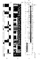
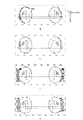
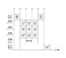
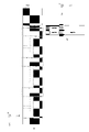
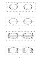
- plan view from the first layer to the third layer in the substrate in the probe without the shield wiring in the 1st Embodiment of this technique It is an example of the plan view and the sectional view of the 4th layer and the 5th layer in the substrate in a probe without shield wiring in 1st Embodiment of this technique.
- plan view from the first layer to the third layer in the substrate in the probe having three antennas in the first embodiment of the present technique It is an example of the plan view and the cross-sectional view of the 4th layer and the 5th layer in the substrate in the probe in which the number of antennas is 3 in the 1st Embodiment of this technique.
- plan view from the first layer to the third layer in the substrate in the probe in which there is no shield wiring and the number of antennas is three in the first embodiment of the present technique.
- plan view and the cross-sectional view of the fourth layer and the fifth layer in the substrate in the probe in which there is no shield wiring and the number of antennas is three in the first embodiment of the present technique.
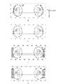
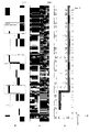
- plan view from the 4th layer to the 6th layer among the 7 layers in the substrate in the probe in the 1st embodiment of the present technique It is an example of the plan view of the 7th layer in the substrate in a probe and the cross-sectional view of a substrate in the 1st Embodiment of this technique. It is an example of the plan view from the first layer to the third layer among the nine layers in the substrate in the probe in the first embodiment of the present technique. It is an example of the plan view from the 4th layer to the 6th layer among the 9 layers in the substrate in the probe in the 1st embodiment of the present technique.
- plan view from the 7th layer to the 9th layer among the 9 layers in the substrate in the probe in the 1st embodiment of the present technique It is an example of the cross-sectional view of the substrate in the probe of the 9-layer structure in the 1st Embodiment of this technique. It is a figure for demonstrating the influence which the width of the substrate in a probe and the cross-sectional area of a probe housing have on the measurement of water content in 1st Embodiment of this technique from two viewpoints. It is an example of the plan view from the first layer to the third layer in the substrate in the probe which formed the slot in the 1st Embodiment of this technique.
- plan view and the sectional view of the 4th layer and the 5th layer in the substrate in the probe which formed the slot in the 1st Embodiment of this technique It is an example of the plan view from the first layer to the third layer in the substrate in the probe which formed the slot in the 1st Embodiment of this technique and eliminated the shield wiring. It is an example of the plan view and the cross-sectional view of the 4th layer and the 5th layer in the substrate in the probe which formed the slot in the 1st Embodiment of this technique and eliminated the shield wiring. It is an example of the plan view from the first layer to the third layer in the substrate in the probe which formed the slot and provided three antennas in the 1st Embodiment of this technique.
- plan view and the sectional view of the 4th layer and the 5th layer in the substrate in the probe which formed the slot and provided 3 antennas in the 1st Embodiment of this technique It is an example of the plan view from the first layer to the third layer in the substrate in the probe which formed the slot, eliminated the shield wiring, and provided three antennas in the 1st Embodiment of this technique. It is an example of the plan view and the cross-sectional view of the fourth layer and the fifth layer in the substrate in the probe provided with three antennas by forming a slot and eliminating the shield wiring in the first embodiment of the present technique. ..
- plan view from the 1st layer to the 3rd layer among the 7 layers in the substrate in the probe which formed the slot in the 1st Embodiment of this technique It is an example of the plan view from the 4th layer to the 6th layer among the 7 layers in the substrate in the probe which formed the slot in the 1st Embodiment of this technique. It is an example of the cross-sectional view of the 7th layer and the substrate in the substrate in the probe which formed the slot in the 1st Embodiment of this technique. It is an example of the plan view from the 1st layer to the 3rd layer among the 9 layers in the substrate in the probe which formed the slot in the 1st Embodiment of this technique.
- plan view from the 4th layer to the 6th layer among the 9 layers in the substrate in the probe which formed the slot in the 1st Embodiment of this technique It is an example of the plan view from the 7th layer to the 9th layer among the 9 layers in the substrate in the probe which formed the slot in the 1st Embodiment of this technique.
- the cross-sectional view of the probe housing 320 when viewed from above in the fourth modification and the comparative example of the first embodiment of the present technique. It is an example of the cross-sectional view of the probe housing when viewed from above in the fifth modification of the first embodiment of the present technique. It is an example of the cross-sectional view of the probe housing in which the wall thickness in the direction parallel to the substrate inside the probe is increased by bilateral radiation in the fifth modification of the first embodiment of the present technique. It is an example of the cross-sectional view of the probe housing in which the wall thickness in the direction perpendicular to the substrate inside the probe is increased by bilateral radiation in the fifth modification of the first embodiment of the present technique.
- the transmitter in the 6th modification of 1st Embodiment of this technique is a plurality of sensor devices.
- FIG. 5 is a diagram showing another example of a cross-sectional view of a sensor device in which the probe in the seventh embodiment of the present technique has three sensors.
- Ninth embodiment (example of inserting a guide before inserting the sensor device) 10.
- a tenth embodiment (an example including a spiral member or a shovel type housing) 11.
- Eleventh embodiment (example of adjusting transmission power) 12.
- Twelfth Embodiment (Example of arranging the measurement unit substrate at a position where the extending direction of the probe and the substrate plane are perpendicular to each other)
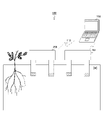
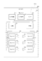
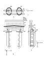
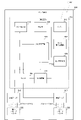
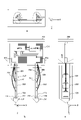
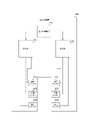
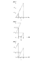
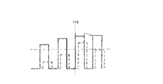
- FIG. 1 is an example of an overall view of the moisture measurement system 100 according to the first embodiment of the present technology.
- the water content measuring system 100 measures the amount of water contained in the medium M, and includes a central processing unit 150 and at least one sensor device such as a sensor device 200 or 201.
- the medium M for example, soil for growing agricultural products is assumed.
- the sensor device 200 acquires data necessary for measuring the amount of water as measurement data. The contents of the measurement data will be described later.
- the sensor device 200 transmits measurement data to the central processing unit 150 via a communication path 110 (such as a wireless communication path).
- the configuration of the sensor device 201 is the same as that of the sensor device 200.
- the central processing unit 150 measures the water content using the measurement data.
- the communication path 110 may be a wired communication path.
- a plurality of central processing units 150 can be provided in the moisture measurement system 100.
- the user applies a load to the sensor devices 200 and 201 from above the soil and inserts them into the soil for use.
- the sensor device 200 or the like is used by exposing at least the antenna portion of the sensor device 200 or the like above the soil surface so as to be able to communicate with the central processing unit 150.
- the gray part in the figure indicates the antenna. If the depth is such that communication with the central processing unit 150 is possible, the above antenna portion may be buried in soil for use.
- the sensor devices 200 and 201 include a pair of probes.
- the length of the probe is 5 to 200 centimeters (cm), and the probe is provided with 1 to 40 antennas, which will be described later. This allows moisture to be measured at multiple depths within the soil depth range of 5 to 200 centimeters (cm).
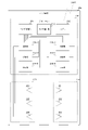
- FIG. 2 is a block diagram showing a configuration example of the central processing unit 150 according to the first embodiment of the present technology.
- the central processing unit 150 includes a central control unit 151, an antenna 152, a central communication unit 153, a signal processing unit 154, a storage unit 155, and an output unit 156.
- the central control unit 151 controls the entire central processing unit 150.
- the central communication unit 153 transmits information (for example, an instruction regarding measurement) to the sensor devices 200 and 201 via the antenna 152, and also receives measurement data from the sensor devices 200 and 201.
- the signal processing unit 154 obtains the water content based on the measurement data.
- the storage unit 155 stores the measurement result of the water content and the like.
- the output unit 156 outputs the measurement result of the water content to a display device (not shown) or the like.
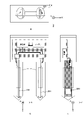
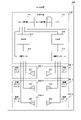
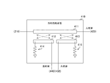
- FIG. 3 is a block diagram showing a configuration example of the sensor device 200 according to the first embodiment of the present technology.
- the sensor device 200 includes a measurement circuit 210, a transmission probe unit 220, and a reception probe unit 230.
- a sensor control unit 211, a sensor communication unit 212, an antenna 213, a transmitter 214, a receiver 215, a transmission switch 216, and a reception switch 217 are arranged in the measurement circuit 210.
- a predetermined number of transmitting antennas such as transmitting antennas 221 to 223 are provided in the transmitting probe unit 220.
- a predetermined number of receiving antennas such as receiving antennas 231 to 233 are provided in the receiving probe unit 230.
- the sensor control unit 211 controls each circuit in the measurement circuit 210.
- the transmission switch 216 selects any of the transmission antennas 221 to 223 according to the control of the sensor control unit 211 and connects to the transmitter 214.
- the reception switch 217 selects any of the reception antennas 231 to 233 according to the control of the sensor control unit 211 and connects to the receiver 215.
- the transmission antennas 221 to 223 are connected to the transmission switch 216 via transmission lines 218-1 to 218-3. Further, the receiving antennas 231 to 233 are connected to the receiving switch 217 via the transmission lines 219-1 to 219-3.
- the transmitter 214 transmits an electric signal having a predetermined frequency as a transmission signal via a selected transmission antenna.
- a CW (Continuous Wave) wave is used as the incident wave in the transmission signal.
- the transmitter 214 transmits a transmission signal in a frequency band of, for example, 1 to 9 gigahertz (GHz) by sequentially switching frequencies in steps of 50 megahertz (MHz).
- the receiver 215 receives the transmitted wave via the selected receiving antenna.
- the transmitted wave is an electromagnetic wave transmitted through the medium between the probes converted into an electric signal by the receiving antenna.
- the sensor communication unit 212 receives the information (instruction regarding measurement) sent from the central processing unit 150, and centrally processes the data indicating the reception result of the receiver 215 as measurement data via the antenna 213. It is to be transmitted to the device 150.
- the configuration of the sensor device 201 is the same as that of the sensor device 200.
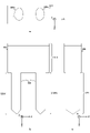
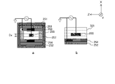
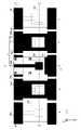
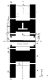
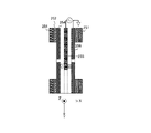
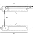
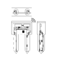
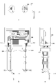
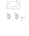
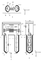
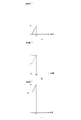
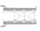
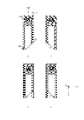
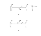
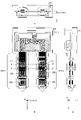
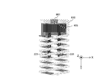
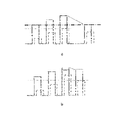
- FIG. 4 is an example of an overall view of the sensor device 200 according to the first embodiment of the present technology.
- a is a transmission diagram viewed from above of the sensor device 200 with the side inserted into the soil facing downward (in other words, a diagram in which the features of each part of the sensor device 200 viewed from above are overlaid).
- b is a front view of the sensor device 200.
- c is a transmission diagram viewed from the side of the sensor device 200 (in other words, a diagram in which the features of each part of the sensor device 200 viewed from the side are overwritten). From this point onward, the three views in the present specification are transparent views (drawings in which the features of each part are overwritten) as in FIG. 4, unless otherwise specified.
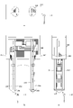
- the sensor device 200 includes a sensor housing 305 provided with a pair of protrusions at the bottom.
- FIG. 5 is an example of an overall view of the sensor housing 305, as will be described later.
- the portion provided with the pair of protrusions is conveniently referred to as a probe housing 320, and the other portion is conveniently referred to as a measuring portion housing 310.
- the housing that houses the transmitting probe unit 220 is called the probe housing 320a
- the housing that houses the receiving probe unit 230 is called the probe housing 320b.
- the combination of the transmission probe unit 220 and the probe housing 320a containing the transmission probe unit 220 is referred to as a transmission probe
- the combination of the reception probe unit 230 and the probe housing 320b containing the transmission probe unit 230 is referred to as a reception probe.
- the measurement unit board 311 is arranged in the measurement unit housing 310.
- the measuring unit board 311 is an electronic board (in other words, a wiring board) provided by laminating a plurality of wiring layers.
- a measurement circuit 210 is formed on the measurement unit substrate 311.
- the measuring unit 312 of FIG. 4 represents the measuring circuit 210 of FIG.
- the antenna 213 is included in the measurement circuit 210.
- the antenna 213 is arranged outside the measurement circuit 210, which represents a modification of the measurement circuit 210 shown in FIG. In FIG. 4, the antenna 213 may be included in the measurement circuit 210.
- a battery 313, a connector 314, and a connector 315 are further connected to the measurement board 311.
- the measuring unit 312, the connector 314, and the connector 315 are connected by a strip line provided with a signal line and a shield layer.
- the three thick white lines indicate the signal lines
- the thick black lines indicate the shield layer for convenience.
- shield wiring between signal lines and arranging shield layers above and below the signal lines in the direction orthogonal to the board plane a strip line shielded between each signal line is formed.
- FIG. 4 it is simplified and displayed.
- the probe inner substrates 321 and 322, the radio wave absorbing units 341 to 346, and the positioning units 351 and 352 are arranged.
- the substrate inside the probe 321 is an electronic board (in other words, a wiring board) provided by laminating a plurality of wiring layers.
- a connector 323, a radiation element 330 to 332, a shield layer 325, and a plurality of signal lines (not shown) are formed on the probe inner substrate 321.
- a plurality of shield layers are formed in the probe inner substrate 321.
- the portion including the radiation element 330 and the portion of the shield layer 325 exposed from the radio wave absorbing portion 341 or the like functions as one transmitting antenna 221.
- the radiating elements 331 and 332 also function as transmitting antennas 222 and 223. In the figure, three transmitting antennas are arranged.
- each of the plurality of signal lines is a shield layer or a shield formed on the substrate 321 in the probe in both the substrate parallel direction (left and right of the signal line) and the substrate vertical direction (upper and lower of the signal line). It is made up of strip lines shielded by wiring or shield vias.
- the measurement unit 312 and the connector 314 are connected by independent transmission lines for each transmission antenna, and these transmission lines are shielded from the signal line provided on the measurement unit board 311. It is formed of strip lines using layers.
- a transmission line (particularly a strip line) independent of each transmitting antenna is connected from the measuring unit 312 to all the transmitting antennas (transmitting antennas 221 to 223 in the examples of FIGS. 3 and 4) provided in the sensor device 200. ) Is connected.
- the board inside the probe 322 is also an electronic board (in other words, a wiring board) provided by stacking a plurality of wiring layers.
- a connector 324, elements (reception elements) 333 to 335, a shield layer 326, and a plurality of signal lines (not shown) are formed on the probe inner substrate 322. Also in the probe inner substrate 322, a plurality of shield layers are formed.
- the portion including the element (reception element) 333 and the portion of the shield layer 326 exposed from the radio wave absorbing portion 344 or the like functions as one receiving antenna 231.
- the radiating elements 334 and 335 also function as receiving antennas 232 and 233. In the figure, three receiving antennas are arranged.
- the connector 324 and the elements (reception elements) 333 to 335 provided in the reception antennas 231 to 233 are connected by transmission lines 219-1 to 219-3 independent for each reception antenna.
- each of the plurality of signal lines is a shield layer or a shield formed on the substrate 322 in the probe in both the substrate parallel direction (left and right of the signal line) and the substrate vertical direction (upper and lower of the signal line). It is made up of strip lines shielded by wiring or shield vias.
- the measurement unit 312 and the connector 315 are connected by independent transmission lines for each receiving antenna, and these transmission lines are shielded from the signal line provided on the measurement unit board 311. It is formed of strip lines using layers.
- a transmission line (particularly a strip line) independent of each transmitting antenna is connected from the measuring unit 312 to all the receiving antennas (received antennas 231 to 233 in the example of FIGS. 3 and 4) provided in the sensor device 200. ) Is connected.
- the portion including the probe housing 320a in FIG. 4 and the substrate inside the probe 321 corresponds to the transmission probe unit 220 in FIG.
- a reinforcing portion 360 is provided between these probe units corresponding to the receiving probe unit 230 in FIG.
- the axis parallel to the direction in which the sensor device 200 is inserted into the soil is defined as the Y axis.
- the probe housings 320a and 320b extend in the Y-axis direction.
- the substrates 321 and 322 in the probe also extend in the Y-axis direction.
- the axis parallel to the Y-axis on the first plane including the center line in the Y-axis direction of the in-probe substrate 321 and the center line in the Y-axis direction in the in-probe substrate 322 is defined as the X-axis. .. In the sensor device 200 shown in FIG.
- the measuring unit substrate 311 extends on a second plane including a line parallel to the X-axis direction and a line parallel to the Y-axis direction.
- the axis perpendicular to the X-axis and the Y-axis is defined as the Z-axis.
- the first and second planes are planes orthogonal to the Z axis.
- the sensor device 200 is a device for measuring the amount of water in the medium based on the characteristics of the electromagnetic wave propagating in the medium between the transmission / reception antennas.
- each of the transmitting antenna and the receiving antenna is planar, and these are formed on an electronic substrate such as a probe inner substrate 321 and 322.
- This configuration is hereinafter referred to as "component (1)".
- component (1) compared to the form in which the antenna is formed of a separate component and then attached to the electronic substrate (probe inner substrate 321, 322), the processing accuracy and mounting accuracy of the antenna are high, and the moisture content can be measured accurately.
- the electronic board and the antenna can be compactly formed, and the cross section of the housing can be made small. As a result, the creation of unnecessary space in the housing has been reduced, which also enables accurate measurement of moisture. The details of this effect will be described later.
- the transmitting antenna and the receiving antenna are fixedly arranged in the sensor housing 305 so as to face each other and the distance between the antennas is a predetermined distance.
- a configuration in which these two antennas are opposed to each other and fixed at a predetermined distance is hereinafter referred to as a “component (2)”.
- the gain of the antenna is improved and the sensitivity is increased as compared with the form in which the planar antennas are not opposed to each other or the two antennas are not fixedly arranged so as to be at a predetermined distance.
- the water content can be measured accurately.
- 219-1 to 219-3 are formed by using an electronic substrate (measurement unit substrate 311 and probe inner substrates 321 and 322). This configuration is hereinafter referred to as "component (3)".
- component (3) This configuration is hereinafter referred to as "component (3)”.
- the sensor device 200 includes the measurement unit substrate 311 and the probe inner substrates 321 and 322 as electronic substrates, and the measurement unit substrate 311 is arranged orthogonal to the probe inner substrates 321 and 322. More specifically, (1) the measuring unit substrate 311 is arranged in parallel with the first plane, and (2) the probe inner substrates 321 and 322 are arranged facing each other and with the first plane. (3) As a result, the measuring unit substrate 311 is arranged orthogonally to the probe inner substrates 321 and 322. This configuration is hereinafter referred to as "component (4)".
- the sensor housing 305 includes the probe housings 320a and 320b, the transmitting antennas are arranged at a plurality of locations along the direction in which the probe housing 320a extends, and the receiving antenna also has the probe housing 320b extending. It is arranged in multiple places along the direction of the antenna. This configuration is hereinafter referred to as "component (5)".
- the transmission lines include a plurality of transmission lines individually connecting the measurement unit 312 provided on the measurement unit board 311 and all the transmission antennas provided on the sensor device 200, and the measurement unit 312 and the sensor provided on the measurement unit board 311. It includes a plurality of transmission lines individually connected to each of all the receiving antennas provided in the device 200.
- the measuring unit 312 provided on the measuring unit board 311 drives a plurality of transmitting antennas and a plurality of receiving antennas in a time-division manner. This configuration is hereinafter referred to as "component (6)".
- a transmission line including a plurality of shielded signal lines, and is between two boards arranged orthogonally via a transmission line which is more flexible than the measurement unit board 311 and 312 (that is, measurement).
- the transmission lines (between the unit substrate 311 and the probe inner substrate 321 and between the measurement unit substrate 311 and the probe inner substrate 322) are connected.
- This configuration is hereinafter referred to as "component (7)".
- This makes it possible to arrange a plurality of planar transmitting antennas and a plurality of planar receiving antennas so as to face each other.
- a high-gain transmit / receive antenna can be used to accurately measure moisture over the entire soil located between a plurality of transmit / receive antennas.
- the probe housings 320a and 320b are formed of an electromagnetic wave transmitting material, and the strength of the probe housings 320a and 320b is higher than the strength of the electronic substrate housed therein. This configuration is hereinafter referred to as "component (8)".
- a transmitting antenna is formed on the probe inner substrate 321 and a receiving antenna is formed on the probe inner substrate 322.
- the probe in a direction orthogonal to the extending direction (Y-axis direction) of the probe housing 320a and the probe inner substrate 321, (1) the probe from the center of the probe inner substrate 321 in the direction perpendicular to the probe inner substrate 321.
- the distance to the housing end of the housing 320a is smaller than the distance (2) from the center of the probe inner substrate 321 to the housing end of the probe housing 320a in the direction parallel to the probe inner substrate 321.
- the sensor device 200 shown in the figure is formed by using a material that absorbs electromagnetic waves, and covers at least a part of a “transmission transmission line connecting between a transmission element (transmission antenna) and a measurement unit”.
- a receiving transmission line formed by using a credit transmission line covering portion and a material that absorbs electromagnetic waves and covers at least a part of a "reception transmission line connecting between a receiving element (reception antenna) and a measuring section”. It is provided with a covering portion.
- the transmission probe unit is provided with the above-mentioned transmission line covering portion for transmission, and the receiving probe unit is also provided with the above-mentioned transmission line covering portion for reception.
- the sensor housing 305 includes a measuring unit housing 310 and a probe housing 320.
- the portion containing the transmitting antenna is the transmitting probe housing 320a
- the portion containing the receiving antenna is the receiving probe housing 320b.
- the transmitting probe housing 320a and the receiving probe housing 320b are fixed to the measuring unit housing 310 and integrated. It should be noted that these can also be in a separated state as described later.
- the sensor housing 305 may be in a form in which the sensor housing 305 is divided into a plurality of parts in advance and then these parts are fixed and integrated. Further, the sensor housing 305 may be in a form in which the transmission probe housing, the reception probe housing, and the measurement unit housing 310 are integrally formed at the time of forming the transmission probe housing, the reception probe housing, and the measurement unit housing 310.
- the sensor housing 305 is provided with a reinforcing portion 360 for improving the strength of the housing, but it is also possible to configure the sensor housing 305 without the reinforcing portion 360.
- the reinforcing portion 360 has a structure in which at least two of the transmitting probe housing 320a, the receiving probe housing 320b, and the measuring unit housing 310 are connected. A structure connected to these three may be used.
- all of the sensor housing 305 may be formed by using a material that transmits electromagnetic waves.
- at least the part closest to the transmitting element (transmitting antenna) and the receiving element (receiving antenna) is formed by using a material that transmits electromagnetic waves, and at least a part of the other parts is made of a material different from the above-mentioned material. May be formed using.
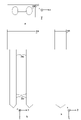
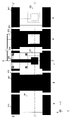
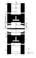
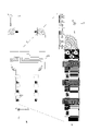
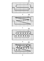
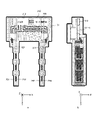
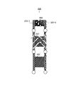
- FIG. 5 is an example of an overall view of the sensor housing 305 according to the first embodiment of the present technology.
- a is a transmission view seen from above the sensor housing 305.
- b is a front view of the sensor housing 305.
- c is a cross-sectional view of the sensor housing 305.
- the housing that houses the transmitting probe unit 220 is called the probe housing 320a
- the housing that houses the receiving probe unit 230 is called the probe housing 320b.
- the reinforcing structure for improving the strength of the housings 320a and 320b is called a reinforcing portion 360.
- the housing part containing the transmitting antenna and the transmitting transmission line and the housing part containing the receiving antenna and the receiving transmission line are these.
- the entire part is made of an electromagnetic wave transmitting material.
- the thickness (magnitude in the Z-axis direction) of the measuring unit housing 310 is the width (magnitude in the X-axis direction) and height (magnitude in the Y-axis direction) of the measuring unit housing 310. ) Is smaller than either.
- the sensor housing 305 including the reinforcing portion 360 is formed of an electromagnetic wave transmitting material.
- the electromagnetic wave transmitting material include polymer materials, glass, and inorganic materials such as PTEF (PolyTEtraFluoroethylene).
- PTEF PolyTEtraFluoroethylene
- PC PolyCarbonate
- PES PolyEtherSulfone
- PEEK PolyEtherEtherKetone
- PSS PolyStyrene Sulfonic acid
- PMMA PolyMethylMethAcrylate
- PET PolyEthylene Terephthalate
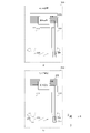
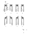
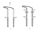
- FIG. 6 is another example of the first embodiment of the present technology, in which the lengths of the transmit probe and the receive probe provided in the sensor devices 200 and 201 are compared with the moisture measurement system 100 shown in FIG.
- This is an example of an overall view of the moisture measurement system 100 in which the number of antennas arranged in the transmitting probe and the receiving probe is increased.
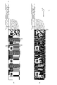
- the moisture measurement system 100 shown in FIG. 6 has a larger length of the transmitting probe and the receiving probe as compared with the moisture measuring system 100 shown in FIG. 1, and the number of antennas arranged in the transmitting probe and the receiving probe. From the moisture measurement system 100 described in FIG. 1, by adding a reinforcing portion 361 that improves the strength of the transmitting probe and the receiving probe, as will be described later with reference to FIGS. 7 and 8. Also, the moisture content of the soil can be measured more accurately in a wider area of the soil (especially in the deep part of the soil).
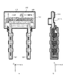
- FIG. 7 is an example of an overall view of the sensor device 200 provided in the moisture measurement system 100 shown in FIG.
- the sensor device 200 shown in FIG. 7 has a larger length of the transmitting probe and the receiving probe and a larger number of antennas arranged in the transmitting probe and the receiving probe as compared with the sensor device 200 shown in FIG.
- it has a structure in which a reinforcing portion 361 for improving the strength of the transmitting probe and the receiving probe is added.
- elements 330 to 339 are provided, and five transmitting antennas and five receiving antennas are formed.
- elements 330 to 334 represent a radiating element, and 335 to 339 represent a receiving element.
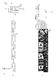
- FIG. 8 is an example of an overall view of the sensor housing 305 provided in the sensor device 200 shown in FIG. 7.
- a reinforcing portion 361 is added to the lower part of the probe housing 320.
- the probe housing 320 If the probe housing 320 is long and the soil is hard, the probe housing 320 will be deformed when the sensor device 200 is stressed and inserted into the soil, and the transmitting antenna and the receiving antenna will be received. The distance to the antenna may be different from the design distance.
- the addition of the reinforcing portion 361 reduces the possibility of its deformation. Further, when the soil is hard, when stress is applied to the sensor device 200 and the sensor device 200 is inserted into the soil, there is a possibility that the space between the measuring unit housing 310 and the probe housing 320 breaks. The addition of the reinforcing portion 361 reduces the possibility of its breakage.
- FIG. 9 is still another example of the first embodiment of the present technology, and is an example of an overall view of the moisture measurement system 100 in which the number of antennas is reduced as compared with the moisture measurement system 100 shown in FIG. Is.
- the number of antennas of the sensor device 200 and the like can be reduced to one on each of the transmitting side and the receiving side.
- the means for driving a plurality of antennas becomes unnecessary. In this case, the components (5) and (6) are unnecessary.
- connection of the transmission line can also be formed by using a metal connector such as an SMA connector. In this case, the component (7) is also unnecessary.
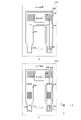
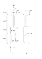
- FIG. 10 is an example of an overall view of the sensor device 200 provided in the moisture measurement system 100 shown in FIG.
- FIG. 11 is an example of an overall view of the sensor housing 305 provided in the sensor device 200 shown in FIG.
- FIG. 12 is still another example of the first embodiment of the present technology, and is an example of an overall view of the moisture measurement system 100 in which the housings provided in the sensor device 200 and 201 are separated into two, respectively. ..
- the measuring unit housing 310 and the probe housing 320 can be separated.
- Each connection between the transmission line formed on the measuring unit board 311 and the transmission line formed on the probe inner boards 321 and 322 is connected by a cable (for example, a coaxial cable).
- the number of antennas in the probe housing 320 is one on the transmitting side and one on the receiving side. In this case, the components (5) to (7) are unnecessary.
- the measuring unit housing 310 and the probe housing 320 are arranged at separate positions, and the directions in which the measuring unit housing 310 is arranged with respect to the soil surface are the probe housings 320a and 320b for which the soil moisture is measured. If it does not affect the rainfall or watering of the soil during the period, the component (4) is also unnecessary.
- FIG. 13 is an example of an overall view of the sensor device 200 provided in the moisture measurement system 100 shown in FIG.
- the number of antennas is one on the transmitting side and one on the receiving side.
- the measuring unit housing 310 containing the measuring unit substrate 311 forms one independent housing.
- the probe housing 320a containing the probe inner substrate forming the transmitting antenna 330 and the probe housing 320b containing the probe inner substrate 322 forming the receiving antenna 331 are connected to each other to provide one independent probe housing. It forms a body 320.
- the probe housing 320 further includes a reinforcing portion 360.
- FIG. 14 is an example of an overall view of the sensor housing 305 provided in the sensor device 200 shown in FIG.
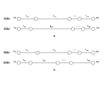
- FIG. 15 is still another example of the first embodiment of the present technology, and is a moisture measurement system in which the housings provided in the sensor devices 200 and 201 are separated and a plurality of probe housings are provided for each sensor device. It is an example of the whole view of 100.
- each of the sensor devices 200 and 201 includes a plurality of transmitting antennas and a plurality of receiving antennas. Then, in each of the sensor devices 200 and 201, one transmitting antenna and one receiving antenna are paired, and a probe housing is provided for each pair of antennas.
- each sensor device 200 is provided with a measurement unit housing 310 and a plurality of probe housings such as probe housings 320, 320-1, and 320-2. ..
- the number of antennas in each probe housing is one on the transmitting side and one on the receiving side. In this case, the components (4) and (7) are unnecessary.
- FIG. 16 is an example of an overall view of the sensor device 200 provided in the moisture measurement system 100 shown in FIG.
- the number of antennas is one on the transmitting side and one on the receiving side.
- FIG. 17 is a block diagram showing a configuration example of the sensor device 200 of FIG.
- the transmitting probe units 220-1 to 220-3 and the receiving probe units 230-1 to 230-3 are arranged in the three separated probe housings.
- One antenna is placed in each of these three pairs of units.
- the transmitting antennas 221 to 223 are arranged in the transmitting probe units 220-1 to 220-3
- the receiving antennas 231 to 233 are arranged in the receiving probe units 230-1 to 230-3.
- These antennas are connected to the measurement circuit 210 via transmission lines independent of each other.
- FIG. 18 is still another example of the first embodiment of the present technology, which includes a plurality of transmitting antennas 330 to 332 and a plurality of receiving antennas (333 to 335), and a probe housing containing these.
- This is another example of the overall view of the sensor device 200 in which the body 320 and the measurement unit housing 310 containing the measurement unit substrate 311 are separated.
- the number of antennas can be set to 3 on the transmitting side and 3 on the receiving side. In this case, the components (4) and (7) are unnecessary.
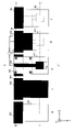
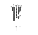
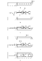
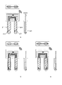
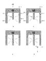
- FIG. 19 shows a front view of the sensor device 200 according to the first embodiment of the present technology (left view of FIG. 19), a transmission antenna 223 provided on the probe inner substrate 321 when the sensor device 200 is viewed from the front, and a transmission antenna 223 thereof.
- This is an example of a sectional view (right figure of FIG. 19) in the vicinity.
- the figure is an example of a cross-sectional view of the transmitting antenna 223 and its vicinity when viewed from the Z-axis direction.
- the colored parts of each layer are, in order from the left side, a radio wave absorber 251, a general solder resist 252, a conductor shield layer 254, a conductor signal line 255, and a conductor shield. It represents a layer 256, a solder resist 253, and a radio wave absorber 251.
- the uncolored layer between the shield layer 254 and the signal line 255 and the uncolored layer between the shield layer 254 and the signal line 255 represent an insulator.
- the solder resist and the insulator transmit electromagnetic waves.
- the number of layers of an electronic board is referred to as the number of layers of a conductor contained in the board. Therefore, the substrate shown on the right side of FIG. 19 is called a three-layer substrate.
- the radio wave absorber 251 and the shield layer 254, the signal line 255, the shield layer 256, and the radio wave absorber 251 are respectively used for convenience. It may be referred to as a first layer, a second layer, a third layer, a fourth layer, and a fifth layer.
- the cross-sectional views of the transmitting antennas 221 and 222 are the same as those of the transmitting antenna 223. When the direction from the transmitting side to the receiving side is to the right in the X-axis direction, the cross-sectional view of the receiving antennas 231 to 233 is symmetrical with the transmitting antenna 223.
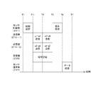
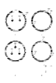
- FIG. 20 is an example of a plan view for each layer of the transmitting antenna 223 and its vicinity, the cross section of which is shown in the right figure of FIG.
- the figure shows a plan view of the transmission antenna 223 shown on the right side of FIG. 19 and its vicinity for each layer when viewed from the X-axis direction of the sensor device 200.
- a is a plan view of the first layer: the radio wave absorber 251 in the right figure of FIG.
- b is a plan view of the second layer: the shield layer 254.
- c is a plan view of the third layer: signal line 255.
- d is a plan view of the fourth layer: the shield layer 256.
- e is a plan view of the fifth layer: the radio wave absorber 251.
- the cross-sectional view when cut along the AA'line corresponds to the cross-sectional view of FIG.
- the second layer shown in FIG. 20b is the first wiring layer to which the shield layer 254 is wired.
- the third layer shown in FIG. 20c is a second wiring layer to which the linear signal line 255 is wired.
- the fourth layer shown in FIG. 20d is a third wiring layer to which the shield layer 256 is wired.
- Dz be the width of the signal line 255 in the Z-axis direction.
- the symbol connecting the square and its diagonal line by a line segment described in FIGS. 20b, c, and d is a via (reference numeral 257 in FIG. 21a) connecting the shield layer 254 shown in FIG. 20b and the shield layer 256 shown in FIG. 20d. show.
- FIGS. 21a reference numeral 257 in FIG. 21a
- the symbol represents the position of the via 257 connecting the shield layer 254 and the shield layer 256.
- the symbol represents a state in which the via 257 passes by the side of the signal line 255. Due to this via 257, the shield layer 254 and the shield layer 256 have the same potential.
- the dotted line on the side closer to "A" shown in FIG. 20c is the outline of the radio wave absorber 251 shown in FIG. 20e projected onto FIG. 20c for convenience. Is.
- the dotted line on the side close to "A'" shown in FIG. 20c is the outline of the shield layer 256 shown in FIG. 20d projected onto FIG. 20c for convenience.
- the dotted lines shown in FIGS. 20d and e are the outlines of the signal lines 255 shown in FIG. 20c projected onto FIGS. 20d and e for convenience.
- FIG. 21 is an example of a cross-sectional view of the transmitting antenna 223 and its vicinity, which is shown in the cross-sectional view on the right side of FIG. 19, when viewed from above.
- 21 is a cross-sectional view taken along the line BB'of FIG. 20, and b in FIG. 21 is a cross-sectional view taken along the line CC'of FIG. 20. be.
- the cross section of the receiving probe is the same as that of the transmitting probe.
- the transmission probe is covered with a radio wave absorber 251.
- the radio wave absorbing material 251 forms a radio wave absorbing unit 341 and the like.
- solder resists 252 and 253 are formed between both sides of the probe inner substrate 321 and the radio wave absorber 251.
- the probe inner substrate 321 is formed with a wiring layer in which the shield layer 254 is wired, a wiring layer in which the signal line 255 is wired, and a wiring layer in which the shield layer 256 is wired.
- the signal line 255 functions as a radiation element in the transmitting antenna, as described below. Let Dx be the thickness of the wiring layer to which the signal line 255 serving as the radiation element is wired.
- a ground potential is supplied to the shield layers 254 and 256, and the signal line 255 transmits and radiates an AC signal (transmission signal) which is a transmission wave transmitted from the transmission antenna.
- the signal line 255 that transmits and radiates a transmission wave may be referred to as a signal line layer.
- a portion particularly related to the radiation of the transmitted wave may be referred to as a radiation element.
- the signal line 255 that receives and transmits the received wave may be called a signal line or a signal line layer, and the electromagnetic wave received by the receiving antenna among the conductors 255.
- the part related to the reception of (received wave or received signal) may be called a receiving element.
- the back surface side (the side in which the shield layer 254 is arranged) of the substrate with respect to the signal line layer.
- the shield layer 254 and the shield layer 256 are arranged on both the surface side and the surface side (the side on which the shield layer 256 is arranged) via an insulator between the shield layer 254 and the signal line layer.
- This transmission line (transmission line for transmission) is independently wired for each antenna in the probe inner substrate 321 from all the transmission antennas provided in the probe inner substrate to the connector 323.
- a similar transmission line (reception transmission line) is independently wired for each antenna on the probe inner substrate 322 from all the receiving antennas provided on the probe inner substrate to the connector 324.
- the first layer the back side radio wave absorber 251 and the second layer: the shield layer 254 and the third layer related to the transmission and radiation (or reception) of the electromagnetic wave and the shield and the absorption of the electromagnetic wave.
- the signal line layer (signal line 255), the fourth layer: the shield layer 256, and the fifth layer: the surface side electromagnetic wave absorber 251 will be further described.
- the direction toward the transmitter (transmitter provided in the measuring unit) of the transmitted wave is referred to as the transmitter direction, and the direction away from the transmitter is conveniently referred to as the tip direction or simply the destination direction.
- the receiving destination direction the direction in which the signal (received wave) received by the receiving antenna approaches the receiving destination (receiver provided in the measuring unit)
- the direction away from the receiving destination is the tip direction or simply the destination direction.
- the conductor is exposed in space
- the conductor is exposed in space
- a part of the shield layer 256 is exposed from the surface side electromagnetic wave absorber 251 even before the tip of the surface side electromagnetic wave absorber 251.
- a part of the shield layer 256 is exposed in the space.
- a part of the signal line layer (signal line 255) is exposed from the shield layer 256 even before the tip of the shield layer 256. In other words, a part of the signal line layer is exposed in the space.
- the portion exposed from the shield layer 256 functions as a radiating element that transmits a transmitted wave.
- the part of the signal line layer exposed from the shield layer 256 is an electromagnetic wave (transmitted wave propagating in the medium from the transmitting antenna, in other words, received wave).
- the radiating element 332 corresponds to this.
- the receiving element 335 corresponds to this.
- the transmitted wave is perpendicular to this surface. It is most radiated in the direction.
- the direction in which this transmitted wave is radiated most is called the "direction of main radiation” or simply the “direction of radiating electromagnetic waves”.
- a portion of the shield layer that is exposed from the electromagnetic wave absorber 251 (in other words, exposed to the space) and is arranged in the direction of radiating the electromagnetic wave from the radiating element is “shielded”. It is referred to as “exposed part” or simply “shield part”.
- These shield exposed parts and radiating elements function as a transmitting antenna 223.
- the length of the radiating element in the Y-axis direction be Dy.
- the length equal to or less than the length Dy of the radiation element, especially from the line end of the shield exposed part in the transmission source direction (negative direction of the Y axis in FIGS. 19 and 20).
- the portion arranged in the region functions particularly effectively as a part of the transmitting antenna 223. Therefore, in the present specification, of the (1) radiation element (signal line layer exposed from the shield layer and exposed to the space) and (2) the shield exposed portion exposed from the electromagnetic wave absorber and exposed to the space.
- a structure consisting of a portion arranged in a region having the same length as or within the radiation element in the transmission source direction (negative direction of the Y axis in FIGS. 19 and 20) from the tip of the shield exposed portion.
- the shield is exposed.
- a portion consisting of a structure arranged in a region having the same length as or within the receiving element in the receiving destination direction (negative direction of the Y axis in FIGS. 18 and 19) from the tip of the portion and a portion consisting of the receiving antenna. May be called.
- the planar transmitting antenna 223 includes a shield portion and a radiating element.
- the transmitting antenna 223 is formed by using an electronic substrate (such as a probe inner substrate 321) having a plurality of wiring layers.
- the second direction width direction of the electronic substrate, in the figure
- the size Dx in the first direction thickness direction of the electronic substrate, X-axis direction in the figure.
- the size Dz in the Z-axis direction is large.
- the size Dy in the third direction (the length direction in which the electronic substrate extends, the Y-axis direction in the figure) orthogonal to both the first direction and the second direction is larger than the Dx.
- the transmitting antenna when both Dz and Dy of the radiating element provided in the transmitting antenna are larger than Dx, the transmitting antenna is referred to as a “planar antenna” and a “planar transmitting antenna”. Is defined as. A part of the radiating element that extends on a plane determined by the second and third directions is defined as a "plane of the radiating element". Regarding the transmitting antenna, preferably, Dy may be larger than both Dx and Dz. The same applies to the receiving antenna. Explaining the structure of the receiving antenna with reference to FIGS. 19 to 21, the receiving element provided in the receiving antenna has a size Dx in the first direction (thickness direction of the electronic substrate, X-axis direction in the figure) rather than the size Dx.
- the size Dz in the second direction (width direction of the electronic substrate, Z-axis direction in the figure) orthogonal to the first direction is large.
- the size Dy in the third direction (the length direction in which the electronic substrate extends, the Y-axis direction in the figure) orthogonal to both the first direction and the second direction is larger than the Dx.
- the receiving antenna is referred to as a "planar receiving antenna” and a "planar receiving antenna”. Is defined as.
- a part of the receiving element that extends on a plane determined by the second direction and the third direction is defined as a "plane of the receiving element".
- Dy may be larger than both Dx and Dz.
- the periphery of the transmission line including the signal line 255 to which the signal is given and the shield layer 256 to which the ground potential is given is a radio wave. Covered, surrounded or wrapped with absorbent material 251.
- the radio wave absorbing material 251 extends along the extending direction (Y-axis direction) of the transmission line, and an antenna (transmitting antenna or receiving antenna) extends beyond the outer edge of the transmission line covered with the radio wave absorbing material 251. Be connected.
- the antenna is an electronic substrate (such as a substrate in a probe 321) having at least three laminated wiring layers (first, second, and third wiring layers in order from the back surface side to the front surface). Is formed in.
- the antenna comprises a signal line 255 to which a signal is given and shield layers 254 and 256 to which a ground potential is given.
- the signal line 255 to which the signal is given in the antenna is formed in the second wiring layer.
- the shield layer 254 is formed on the first wiring layer, and the shield layer 256 is formed on the third wiring layer.
- the shield layer 254 of the first wiring layer is arranged at the position where the projection of the signal line 255 is arranged.
- electromagnetic waves are radiated from the planar transmitting antenna 223 in the surface direction (to the right of the paper, in the positive direction of the X-axis).
- An antenna in which electromagnetic waves are radiated from one side of the plane of a planar radiating element in this way is called a “one-sided radiating antenna", and in the present specification, this is referred to as a "first structure" of the antenna. ..
- a receiving antenna an antenna in which electromagnetic waves are received from one side of the plane of a planar receiving element is called a "one-sided receiving antenna", and such a receiving antenna corresponds to the first structure.
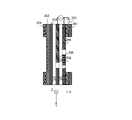
- FIG. 22 is a cross-sectional view showing another example of the first structure when the sensor device 200 according to the first embodiment of the present technology is viewed from the front as in FIG. 4b.
- the figure is an example of a cross-sectional view of the transmitting antenna 223 and its vicinity when viewed from the Z-axis direction.
- FIG. 23 is a plan view of each layer for another example of the first structure, the cross section of which is shown in FIG. 22.
- FIG. 24 is a cross-sectional view of another example of the first structure, the cross section of which is shown in FIG. 22, when viewed from above.
- the first wiring layer (shield layer 254) to which the ground potential is applied is further ahead of the radiation element (signal line 255).
- the extending point is the same as that of the first structure, but (2) radiation is performed by using a second wiring layer that is a part of the second wiring layer and is different from the radiation element and the signal line.
- the point where the conductor 257 to which the ground potential is applied is formed in the region ahead of the element, and (3) the radiation element so that the third wiring layer (shield layer 256) does not overlap with the radiation element. It differs from the first structure in that it extends beyond the radiation element through the side of this projection, avoiding the projection onto the third wiring layer (dotted line in FIG.
- This shape has an effect that when a transmission antenna different from the transmission antenna 223 shown in FIGS. 22 to 24 is arranged, at least the shield layer 256 that gives a ground potential to the transmission antenna can be easily wired. Bring. The same applies to the receiving antenna.
- the first wiring layer (shield layer 254) to which the ground potential is applied extends further beyond the receiving element (signal line 255), which is the same as the first structure.
- a conductor 257 that is a part of the second wiring layer and has a ground potential applied to a region ahead of the receiving element by using a second wiring layer different from the receiving element and the signal line. And (3) avoid projection of the receiving element onto the third wiring layer (dotted line in FIG.
- the third wiring layer shield layer 256
- the third wiring layer shield layer 256
- This shape has an effect that when a receiving antenna different from the receiving antenna 233 shown in FIGS. 22 to 24 is arranged, at least the shield layer 256 that gives a ground potential to the receiving antenna can be easily wired. Bring.
- FIG. 25 is a cross section of a second structure relating to the transmitting antenna 223 provided on the probe inner substrate 321 and its vicinity when the sensor device 200 according to the first embodiment of the present technology is viewed from the front as in FIG. 4b. This is an example of the figure.
- FIG. 24 is an example of a plan view for each layer of the second structure whose cross section is shown in FIG. 25.
- FIG. 27 is an example of a cross-sectional view of the second structure whose cross section is shown in FIG. 25 when viewed from above.
- the shape of the signal line 255 to which the signal is given, which is formed in the second wiring layer, is changed to the back surface side (left direction of the paper surface, negative direction of the X-axis).
- the area where the conductor 254 is not arranged is similar to the third wiring layer arranged on the surface side (right direction of the paper surface, positive direction of the X-axis). At least a portion of the projection of the signal line 255 is extended. Due to this shape, in the transmitting antenna 223 shown in FIG.
- Electromagnetic waves are emitted in both directions.
- An antenna in which electromagnetic waves are radiated from both sides of a plane of a planar radiating element is referred to as a "bilateral radiating antenna", and in the present specification, this is referred to as a "second structure" of the antenna.
- the transmitting antenna having this structure has the effect of being able to radiate electromagnetic waves (transmitted waves) more efficiently than the transmitting antenna having the first structure.
- an antenna in which electromagnetic waves are received from both sides of the plane of the planar receiving element is called an "antenna for receiving on both sides", and such a receiving antenna corresponds to the second structure.
- the receiving antenna having this structure has the effect of being able to receive electromagnetic waves (transmitted waves propagating in the medium from the transmitting antenna, in other words, received waves) more efficiently than the receiving antenna of the first structure. Bring.
- FIG. 28 is a cross-sectional view showing another example of the second structure when the sensor device 200 according to the first embodiment of the present technology is viewed from the front as in FIG. 4b.
- the figure is an example of a cross-sectional view of the transmitting antenna 223 and its vicinity when viewed from the Z-axis direction.
- FIG. 29 is a plan view of each layer for another example of the second structure, the cross section of which is shown in FIG. 28.
- FIG. 230 is a cross-sectional view of another example of the second structure, the cross section of which is shown in FIG. 28, when viewed from above.
- the first wiring layer (shield layer 254) is connected to the first wiring layer of the radiation element so as not to overlap with the radiation element. A point that extends beyond the radiating element through the side of this projection, avoiding the projection (dotted line in FIG. 29b), and (2) part of the second wiring layer.
- a conductor 257 to which a ground potential is applied is formed in the region ahead of the radiating element, and (3) the third wiring.
- FIG. 31 is a cross section of a third structure relating to the transmitting antenna 223 provided on the probe inner substrate 321 and its vicinity when the sensor device 200 according to the first embodiment of the present technology is viewed from the front as in FIG. 4b. This is an example of the figure.
- FIG. 32 is an example of a plan view for each layer of the third structure whose cross section is shown in FIG. 31.
- FIG. 33 is an example of a cross-sectional view of the third structure whose cross section is shown in FIG. 31 when viewed from above.
- the third wiring layer which is the wiring layer on the most surface side (the rightmost side of the paper surface in FIG. 30 and the most positive direction of the X-axis).
- the shield layer 256 is formed by using a part of the third wiring layer.
- the radiation element (conductor 258) is placed in the region ahead of the shield layer 256. It is formed. Then, by providing a via connecting between the radiation element formed by using the third wiring layer and the signal line 255 formed by using the second wiring layer, the radiation element and the signal line 255 are electrically connected. Is connected.
- a colored portion (hatched portion) between the radiating element and the signal line 255 represents this via.
- the symbol connecting the square and its diagonal line by a line segment arranged in the radiation element of FIG. 32d and the same symbol as above arranged in the signal line 255 of FIG. 32c indicate the position of this via.
- the first wiring layer shield layer 254
- the first wiring layer is the wiring layer on the backmost side (the rightmost side of the paper in FIG. 31, the most negative direction of the X-axis) and is given a ground potential, is larger than the radiation element. It is the same as the first structure in that it extends further.
- a radiation element is formed by using the outermost wiring layer (surface wiring layer) on one side of the probe inner substrate 321 forming the transmitting antenna, and this is exposed to the space on one side. It is a radiation antenna.
- the transmitting antenna having this structure has the effect of being able to radiate electromagnetic waves (transmitted waves) more efficiently than the transmitting antenna having the first structure.
- a receiving antenna a receiving element is formed by using the outermost wiring layer (surface wiring layer) on one side of the probe inner substrate 322 forming the receiving antenna, and this is exposed in space, and one-sided reception is performed.
- the antenna corresponds to the third structure.
- the receiving antenna having this structure has the effect of being able to receive electromagnetic waves (transmitted waves propagating in the medium from the transmitting antenna, in other words, received waves) more efficiently than the receiving antenna of the first structure. Bring.
- FIG. 34 is a cross-sectional view showing another example of the third structure when the sensor device 200 according to the first embodiment of the present technology is viewed from the front as in FIG. 4b.
- the figure is an example of a cross-sectional view of the transmitting antenna 223 and its vicinity when viewed from the Z-axis direction.
- FIG. 35 is an example of a plan view for each layer of another example of the third structure whose cross section is shown in FIG. 34.
- FIG. 36 is an example of a cross-sectional view of another example of the third structure, the cross section of which is shown in FIG. 34, when viewed from above.
- the first wiring layer (shield layer 254) to which the ground potential is applied extends further beyond the radiation element.
- the points are the same as those of the third structure, but (2) a second wiring layer that is a part of the second wiring layer and is different from the signal line is used in the region ahead of the signal line.
- the shield layer 256 is lateral to the radiation element. It differs from the third structure in that it extends through and beyond the radiating element.
- This shape has an effect that when a different transmitting antenna is arranged ahead of the transmitting antenna 223 shown in FIGS. 34 to 36, at least the conductor 256 that gives a ground potential to the transmitting antenna can be easily wired. Bring. The same applies to the receiving antenna.
- the first wiring layer (shield layer 254) to which the ground potential is applied extends further beyond the radiation element, which is the same as the third structure, while (2) the second.
- a second wiring layer which is a part of the wiring layer of the above and is different from the signal line, is used to form a conductor 257 to which a ground potential is applied in a region ahead of the signal line.
- the shield layer 256 extends to the front of the radiation element through the side of the receiving element. It differs from the third structure in that it exists. This shape has an effect that when a receiving antenna different from the receiving antenna 223 shown in FIGS. 34 to 36 is arranged, at least the shield layer 256 that gives a ground potential to the receiving antenna can be easily wired. Bring.
- FIG. 37 is a cross section of a fourth structure relating to the transmitting antenna 223 provided on the probe inner substrate 321 and its vicinity when the sensor device 200 according to the first embodiment of the present technology is viewed from the front as in FIG. 4b. This is an example of the figure.
- FIG. 38 is an example of a plan view for each layer of the fourth structure whose cross section is shown in FIG. 37.
- FIG. 39 is an example of a cross-sectional view of the fourth structure whose cross section is shown in FIG. 37 when viewed from above.
- the shield layer 256 is formed by using a part of the third wiring layer.
- a third wiring layer that is a part of the third wiring layer and is different from the shield layer 256 is used to radiate to the region ahead of the shield layer 256. The element is formed. Then, by providing a via connecting between the radiation element formed by using the third wiring layer and the signal line 255 formed by using the second wiring layer, the radiation element and the signal line 255 are electrically connected.
- this first wiring layer which is the wiring layer on the backmost side (the leftmost side of the paper surface in FIG. 37, the most negative direction of the X-axis), this first wiring layer.
- the shield layer 254 is formed by using a part of the above.
- a region prior to the shield layer 254 is used by using the first wiring layer that is a part of the first wiring layer and is different from the shield layer 254.
- a radiating element is formed on the surface. Then, by providing a via connecting between the radiation element formed by using the first wiring layer and the signal line 255 formed by using the second wiring layer, the radiation element and the signal line 255 are electrically connected.
- a radiation element is formed using the outermost wiring layer (surface wiring layer) on both sides of the probe inner substrate 321 forming the transmitting antenna, which is exposed to space on both sides. It is a radiation antenna.
- the transmitting antenna having this structure has the effect of being able to radiate electromagnetic waves (transmitted waves) more efficiently than any transmitting antenna having the first to third structures.
- a receiving antenna a receiving element is formed by using the outermost wiring layer (surface wiring layer) on both sides of the probe inner substrate 322 forming the receiving antenna, and this is exposed in space and is received on both sides.
- the antenna corresponds to the fourth structure.
- the receiving antenna having this structure has the effect of being able to receive electromagnetic waves (transmitted waves propagating in the medium from the transmitting antenna, in other words, received waves) more efficiently than the receiving antenna of the first structure. Bring.
- FIG. 40 is a cross-sectional view showing another example of the fourth structure when the sensor device 200 according to the first embodiment of the present technology is viewed from the front as in FIG. 4b.
- the figure is an example of a cross-sectional view of the transmitting antenna 223 and its vicinity when viewed from the Z-axis direction.
- FIG. 41 is an example of a plan view for each layer of another example of the fourth structure whose cross section is shown in FIG. 40.
- FIG. 42 is an example of a cross-sectional view of another example of the fourth structure, the cross section of which is shown in FIG. 40, when viewed from above.
- the shield layer 254 is lateral to the radiation element.
- the point where the conductor 257 to which the ground potential is given is formed in the region ahead of the above, and (3) the shield layer 256 formed by using the third wiring layer and the shield layer 256 among the radiation elements.
- the shield layers 254 and 256 that give a ground potential to the transmission antenna can be easily wired. Brings the effect. The same applies to the receiving antenna.
- the shield layer 254 extends to the front of the receiving element through the side of the receiving element.
- the conductor 257 to which the ground potential is applied is applied to the region ahead of the signal line.
- the shield layer 256 passes by the side of the receiving element and is ahead of the radiating element.
- FIG. 43 is a diagram showing an example of the shape of the transmitting antenna 223 applied to the first structure in the first embodiment of the present technique.
- the tip of the electromagnetic wave absorber 251 and the tip of the shield layer are at the same position, and the signal line 255 (shown by a solid line) that gives a transmission wave (transmission signal) further from these tips. Radiant element) is exposed.
- the transmission antenna 223 may be configured so that the shield layer 256 (shield portion) is not exposed from the tip of the electromagnetic wave absorber 251.
- the signal line 255 (in other words, the radiation element shown by the solid line) exposed from the tip of the electromagnetic wave absorber 251 is shown by a dotted line below the paper surface of the electromagnetic wave absorber 251. It can also be the same width as the strip line (signal line 255).
- the vertical direction of the paper surface is the main radiation direction (X-axis direction) of the radio wave.
- the shape of the receiving antenna 233 may be the shape shown in FIG. 43a. In this case, the radiating element in the transmitting antenna 223 becomes the receiving element in the receiving antenna 233. By using this antenna facing the transmitting antenna and the receiving antenna, the gain of the antenna is improved.
- the width of the radiating element shown by the solid line can be made wider than the width of the strip line (signal line 255) shown by the dotted line.
- a radial element having a meander structure can also be formed.
- a spiral radiating element can also be formed.
- the shape of b to e in the figure can improve the gain in the main radiation direction as compared with a in the figure. Due to the shape of f in the figure, impedance matching can be achieved more than b in the figure, and radio waves can be radiated more efficiently.
- the shape of the receiving antenna 233 may be the shape shown in FIGS. 43a to 43f. In this case, the radiating element in the transmitting antenna 223 becomes the receiving element in the receiving antenna 233.
- FIG. 44 is a diagram showing another example of the shape of the transmitting antenna 223 applied to the first structure in the first embodiment of the present technique.
- a to f in FIG. 44 correspond to those in which the shield layer 256 (shield portion) is exposed from the tip of the electromagnetic wave absorber 251 in a to f in FIG. 43.
- a high frequency current also flows in the shield layer in the main radiation direction and becomes a part of the antenna, so that the gain is improved as compared with a in FIG. 43.
- the shapes b to e in FIG. 44 can improve the gain in the main radiation direction as compared with a in the figure. Due to the shape of f in the figure, impedance matching can be achieved more than b in the figure, and radio waves can be radiated more efficiently.
- the shape of the receiving antenna 233 may be the shape shown in FIGS. 44a to 44f. In this case, the radiating element in the transmitting antenna 223 becomes the receiving element in the receiving antenna 233.
- each of the shapes of FIGS. 43 and 44 can be applied to the second structure.
- FIG. 45 is a diagram showing an example of the shape of the transmitting antenna 223 applied to the third structure in the first embodiment of the present technique.
- the tip of the electromagnetic wave absorber 251 and the tip of the shield layer are at the same position, and the signal line 255 (radiation element) that gives a transmission wave (transmission signal) further from these tips is. It is exposed.
- the transmission antenna 223 may be configured so that the shield layer 256 (shield portion) is not exposed from the tip of the electromagnetic wave absorber 251.
- the width of the radiating element can be made wider than the width of the strip line shown by the dotted line.
- a radial element having a meander structure can also be formed.
- a spiral radiating element can also be formed.
- the shapes b to d in FIG. 45 can improve the gain in the main radiation direction as compared with a in the figure. Due to the shape of e in the figure, impedance matching can be achieved more than a in the figure, and radio waves can be radiated more efficiently.
- the shape of the receiving antenna 233 may be the shape shown in FIGS. 45a to 45e. In this case, the radiating element in the transmitting antenna 223 becomes the receiving element in the receiving antenna 233.
- FIG. 46 is a diagram showing another example of the shape of the transmitting antenna 223 applied to the third structure in the first embodiment of the present technique.
- a to e in FIG. 46 correspond to those in which the shield layer 256 (shield portion) is exposed from the tip of the electromagnetic wave absorber 251 in a to e in FIG. 45.
- a high frequency current also flows in the shield layer in the main radiation direction and becomes a part of the antenna, so that the gain is improved as compared with a in FIG. 45.
- the shapes b to d in FIG. 46 can improve the gain in the main radiation direction as compared with a in the figure. Due to the shape of e in the figure, impedance matching can be achieved more than a in the figure, and radio waves can be radiated more efficiently.
- the shape of the receiving antenna 233 may be the shape shown in FIGS. 46a to 46e. In this case, the radiating element in the transmitting antenna 223 becomes the receiving element in the receiving antenna 233.
- each of the shapes of FIGS. 45 and 46 can be applied to the fourth structure.
- FIG. 47 is a cross-sectional view of the transmitting antenna 233 applied to the third structure in the first embodiment of the present technology as seen from the front as in FIG. 4b.
- a in FIG. 47 corresponds to a cross-sectional view of a in FIG. 46 when viewed from the front (Z-axis direction).
- the radiating element (conductor 258) is formed by using the surface layer of the substrate 321 in the probe.
- the radiation element 258 may be formed by using the inner layer of the probe inner substrate 321 without using the surface layer.
- both conductors 258 and 259 can also be formed using an inner layer, as illustrated in c in the figure.
- FIG. 48 shows a transmission antenna 223 provided on the probe inner substrate 321 and a transmission antenna 223 thereof when the sensor device 200 according to the first embodiment of the present technology is viewed from the front (viewed from the Z-axis direction) as in FIG. 4b. It is an example of the cross-sectional view of the fifth structure about the neighborhood.
- FIG. 49 is an example of a plan view for each layer of the fifth structure whose cross section is shown in FIG. 48.
- FIG. 50 is an example of a cross-sectional view of the fifth structure whose cross section is shown in FIG. 48 when viewed from above.
- the transmitting antenna 223 having the fifth structure shown in FIGS. 48 to 50 is obtained by changing the transmitting antenna 232 having the first structure shown in FIGS. 19 to 21 to a flat and slot-shaped antenna.
- the “planar and slot-shaped antenna” is a shield layer exposed from the electromagnetic wave absorber 251 and exposed to the space, and is a shield layer provided with a slot (in the example of FIGS. 48 to 50, the shield layer is exposed.
- the shield layer 256 serves as a radiating element.
- the "planar and slot-shaped antenna” has a slot sandwiching the radiating element 256, a dielectric (or an insulator), and the dielectric (or an insulator).
- a receiving antenna it is a shield layer exposed from the electromagnetic wave absorber 251 and exposed to the space.
- the shield layer provided with the slot serves as the receiving element 256.
- the “planar and slot-shaped antenna” is a dielectric (or insulation) with this receiving element.
- the uncolored layer arranged between the signal line 255 and the shield layer 256 (radiating element 256) corresponds to the dielectric (or insulator).
- the planar and slot-shaped antenna is formed on an electronic board (such as a probe inner board 321) having a plurality of wiring layers. Then, the size of the radiation element (shield layer 256 having a slot) in the first direction (thickness direction of the electronic substrate, the X-axis direction in FIG. 50) (in other words, the size of the slot provided in the radiation element in the above direction). ) Slot size Dz in the second direction (width direction of the electronic substrate, Z-axis direction in FIG. 49) orthogonal to the first direction and the third direction (electrons) orthogonal to the first and second directions than Dx.
- an electronic board such as a probe inner board 3211 having a plurality of wiring layers.
- both the size Dy of the slot in the length direction in which the substrate extends and the y-axis direction in FIG. 50 are large.
- this transmitting antenna is used for the radiation element (shield layer 256 in the example of FIGS. 48 to 50) provided in the transmitting antenna having a slot. It is defined as “planar and slotted antenna” and “planar and slotted transmitting antenna”. A part of the radiating element that extends on a plane determined by the second and third directions is defined as a "plane of the radiating element”. Further, the quadrangular region determined by the slot width Dz and the slot length Dy shown in FIG. 49d is defined as the region of the transmitting antenna for convenience.
- the receiving antenna when both Dz and Dy are larger than Dx, this receiving antenna is referred to. It is defined as “planar and slot antenna” and “planar and slot receiving antenna”. A part of the receiving element that extends on a plane determined by the second direction and the third direction is defined as a "plane of the receiving element”. Further, the rectangular area defined by the slot width Dz and the slot length Dy shown in FIG. 49d is defined as the receiving antenna area for convenience. With respect to the transmitting antenna and the receiving antenna, Dy may be larger than both Dx and Dz.
- the first wiring layer (shield layer) on the backmost side (negative direction of the X-axis) is formed in the probe inner substrate on which the "planar and slot-shaped antenna" is formed.
- No slot is formed in 254), and a slot is formed in the third wiring layer on the outermost surface side (positive direction of the X-axis). Due to such a shape, the flat and slot-shaped antenna of the fifth structure becomes a one-sided radiation antenna.
- FIG. 51 is a cross-sectional view showing another example of the fifth structure when the sensor device 200 according to the first embodiment of the present technology is viewed from the front (viewed from the Z-axis direction) as in FIG. 4b. Is.
- FIG. 52 is an example of a plan view for each layer of another example of the fifth structure whose cross section is shown in FIG. 51.
- FIG. 53 is an example of a cross-sectional view of another example of the fifth structure, the cross section of which is shown in FIG. 51, when viewed from above.
- FIG. 54 is a cross section showing still another example of the fifth structure when the sensor device 200 according to the first embodiment of the present technology is viewed from the front (viewed from the Z-axis direction) as in FIG. 4b. It is a figure.
- FIG. 55 is an example of a plan view of each layer for yet another example of the fifth structure, the cross section of which is shown in FIG. 54.
- FIG. 56 is an example of a cross-sectional view of the fifth structure, the cross-sectional view of which is shown in FIG. 54, when viewed from above.
- the signal line 255 provided in the “planar and slotted antenna” is 50 in a region further ahead of the slot provided in this antenna. It can also be terminated by connecting to ground via a resistor 260 such as ohm ( ⁇ ). Further, as illustrated in FIGS. 54 to 56, as still another example of the fifth structure, the signal line 255 provided in the "planar and slot-shaped antenna” is further further beyond the slot provided in this antenna. Can also be terminated by connecting to another antenna 261.
- FIG. 57 shows a transmission antenna 223 provided on the probe inner substrate 321 and a transmission antenna 223 thereof when the sensor device 200 according to the first embodiment of the present technology is viewed from the front (viewed from the Z-axis direction) as in FIG. 4b.
- FIG. 58 is an example of a plan view for each layer of the sixth structure whose cross section is shown in FIG. 57.
- FIG. 59 is an example of a cross-sectional view of the sixth structure whose cross section is shown in FIG. 57 when viewed from above.
- the transmitting antenna 223 of the sixth structure shown in FIGS. 57 to 59 is obtained by changing the planar and slot-shaped antenna of the fifth structure shown in FIGS. 48 to 50 to a bilateral radiating antenna.
- the "planar and slot-shaped antenna" of the sixth structure is a shield layer exposed from the electromagnetic wave absorber 251 and exposed to the space, and is a shield layer having a slot (shield layers 256 and 254). ) Is the radiation element. Due to such a shape, the planar and slot-shaped antenna of the sixth structure becomes a bilateral radiation antenna. The same applies to the receiving antenna.
- the "planar and slot-shaped antenna” of the sixth structure shown in FIGS. 57 to 59 is a shield layer exposed from the electromagnetic wave absorber 251 and exposed to the space, and is provided with a slot.
- the shield layer (shield layers 256 and 254) serves as a receiving element.
- FIG. 60 is a cross-sectional view showing another example of the sixth structure when the sensor device 200 according to the first embodiment of the present technology is viewed from the front (viewed from the Z-axis direction) as in FIG. 4b. Is.
- FIG. 61 is an example of a plan view for each layer of another example of the sixth structure, the cross section of which is shown in FIG. 60.
- FIG. 62 is an example of a cross-sectional view of another example of the sixth structure, the cross section of which is shown in FIG. 60, when viewed from above.
- FIG. 63 is a cross section showing still another example of the sixth structure when the sensor device 200 according to the first embodiment of the present technology is viewed from the front (viewed from the Z-axis direction) as in FIG. 4b. It is a figure.
- FIG. 64 is an example of a plan view for each layer of yet another example of the sixth structure, the cross section of which is shown in FIG. 63.
- FIG. 65 is an example of a cross-sectional view of the sixth structure, the cross-sectional view of which is shown in FIG. 63, when viewed from above.
- the signal line 255 provided in the “planar and slotted antenna” is 50 in a region further ahead of the slot provided in this antenna. It can also be terminated by connecting to ground via a resistor 260 such as ohm ( ⁇ ). Further, as illustrated in FIGS. 63 to 65, as still another example of the sixth structure, the signal line 255 provided in the "planar and slot-shaped antenna” is further further beyond the slot provided in this antenna. Can also be terminated by connecting to another antenna 261.
- FIG. 66 shows a flat surface and a slot provided on the probe inner substrate 321 when the sensor device 200 according to the first embodiment of the present technology is viewed from the front (viewed from the Z-axis direction) as in FIG. 4b.
- FIG. 67 is an example of a plan view for each layer of the seventh structure whose cross section is shown in FIG. 66.
- FIG. 68 is an example of a cross-sectional view of the seventh structure whose cross section is shown in FIG. 66 when viewed from above.
- the planar and slot-shaped transmitting antenna 223 having the seventh structure shown in FIGS. 66 to 68 differs from the transmitting antenna 223 having the fifth structure in the following points. That is, in the planar and slot-shaped transmitting antenna 223 having the seventh structure, the region beyond the point where the signal line 255 extending from the source direction crosses a part of the slot (in other words, the source direction). The area beyond the point where the signal line 255 extending from the slot is superimposed on a part of the slot, and within the area near the slot (more preferably, the width Dz of the slot and the length Dy of the slot).
- the signal line 255 is provided with a slotted radiating element (shield layer 256) via the vias shown in the shaded area in FIG. ) Is connected and terminated.
- the flat and slot-shaped antenna having the seventh structure increases the current flowing from the signal line 255 to the radiating element 256 across the slot as compared with the antenna of the fifth structure, resulting in an electromagnetic wave. Can be radiated efficiently.
- the "planar and slot-shaped antenna" of the seventh structure shown in FIGS. 66 to 68 is a shield layer exposed from the electromagnetic wave absorber 251 and exposed to the space, and is provided with a slot.
- the shield layer 256 serves as a receiving element.
- FIG. 69 shows a transmission antenna 223 provided on the probe inner substrate 321 and a transmission antenna 223 thereof when the sensor device 200 according to the first embodiment of the present technology is viewed from the front (viewed from the Z-axis direction) as in FIG. 4b.
- FIG. 70 is an example of a plan view for each layer of the eighth structure whose cross section is shown in FIG. 69.
- FIG. 71 is an example of a cross-sectional view of the eighth structure whose cross section is shown in FIG. 69 when viewed from above.
- the transmitting antenna 223 of the eighth structure shown in FIGS. 69 to 71 is obtained by changing the planar and slot-shaped antenna of the seventh structure shown in FIGS. 66 to 68 to a bilateral radiating antenna.
- the "planar and slot-shaped antenna" of the eighth structure is a shield layer exposed from the electromagnetic wave absorber 251 and exposed to the space, and is a shield layer having a slot (shield layers 256 and 254). ) Is the radiation element. Further, the area beyond the point where the signal line 255 extending from the source direction crosses a part of the slot (in other words, the point where the signal line 255 extending from the source direction is superimposed on the part of the slot).
- the transmitting antenna which is conveniently defined by a rectangular region that is in the region ahead of the slot and is in the vicinity of the slot (more preferably, the width Dz of the slot and the length Dy of the slot).
- the signal line 255 is connected and terminated to both the radiating elements (shield layers 256 and 254) with slots via vias shown by diagonal lines in FIG. Due to such a shape, the planar and slot-shaped antenna of the eighth structure becomes a bilateral radiation antenna.
- the "planar and slot-shaped antenna" of the eighth structure shown in FIGS. 69 to 71 is a shield layer exposed from the electromagnetic wave absorber 251 and exposed to the space, and is provided with a slot.
- the shield layer (shield layers 256 and 254) serves as a receiving element.
- FIG. 72 is a diagram showing an example of the shape of the transmitting antenna applied to the fifth structure of the planar and slot-shaped antenna in the first embodiment of the present technique.
- the shield layer 256 exposed from the electromagnetic wave absorber 251 the entire region overlapping with the signal line 255 can be made into a slot.
- the line width of the signal line 255 exposed from the electromagnetic wave absorber 251 is made larger than the width of the signal line 255 extending to the region where the electromagnetic wave absorber 251 is arranged, and In the shield layer 256, the entire region overlapping with the signal line 255 having an increased width can be made into a slot.
- the signal line 255 exposed from the electromagnetic wave absorber 251 is used as a meander structure, and the entire region of the shield layer 256 that overlaps with the signal line 255 having this meander structure is used as a slot. You can also do it.
- the slot provided in the shield layer 256 exposed from the electromagnetic wave absorber 251 may cross the signal line 255 exposed from the electromagnetic wave absorber 251.
- the slot provided in the shield layer 256 exposed from the electromagnetic wave absorber 251 crosses the signal line 255 exposed from the electromagnetic wave absorber 251 and the slot is the signal line 255. It is also possible to branch the slot (for example, to branch in a T shape) in the area beyond the cross.
- the vertical direction of the paper surface becomes the main radiation direction of the radio wave, and the gain of the antenna is improved. Due to the shapes of b and c in the figure, the radiation resistance is larger than that in a in the figure, so that radio waves can be efficiently emitted. Due to the shape of e in the figure, the radiation resistance is larger than that of d in the figure, so that radio waves can be efficiently emitted.
- the shape a in the figure can be applied to the sixth structure of the flat and slot-shaped antenna.
- impedance matching is easier to obtain and efficient radiation can be achieved as compared with the case where a in the figure is applied to the fifth structure.
- FIG. 73 is a diagram showing an example of the shape of the transmitting antenna applied to the seventh structure of the planar and slotted antenna in the first embodiment of the present technique.
- 73 a to e are terminated by connecting the tip of the signal line 255 of a to e in FIG. 72 to a radiating element (in other words, a slot to be shielded layer 256) via a via.
- a circle indicates a via.
- FIG. 74 is a diagram showing an example of the shape of the transmitting antenna applied to the eighth structure of the planar and slotted antenna in the first embodiment of the present technique.
- FIG. 75 is a diagram for explaining the operating principle of the sensor device 200 in the first embodiment of the present technology and the effect brought about by the structure of the sensor device 200.
- the sensor device 200 of the present technology fixes the distance between the transmitting antenna 221 and the receiving antenna 231 at a predetermined distance d0. Focusing on the fact that the propagation time required for an electromagnetic wave to propagate this predetermined distance d0 increases in proportion to the amount of water in the medium between the transmitting antenna 221 and the receiving antenna 231, the propagation delay time of the electromagnetic wave ⁇ t is measured to determine the water content.
- the sensor device 200 includes a flat or flat and slit-shaped transmitting antenna 221 and receiving antenna 231 having high gain.
- the processing accuracy and positioning accuracy of these antennas are improved, and the environment around the antenna and the transmission line (for example, the size of the space around the antenna and the transmission line, the distance from the antenna and the transmission line to the housing, and the like.
- the transmitting antenna and the transmission path connected to the transmitting antenna are formed by using the same first electronic board (board 321 in the probe), and the receiving antenna and the receiving antenna are formed.
- the transmission path connected to the receiving antenna is formed by using the same second electronic board (board in probe 322).
- the sensor device 200 has a novel structure so that the time for the electromagnetic wave to propagate from the transmitting antenna to the receiving antenna and the magnitude of the propagating signal are always constant). That is, as illustrated in b in the figure, the sensor device 200 includes a transmitting antenna and a receiving antenna that are planar, planar, and slot-shaped, and the planes of these antennas face each other to fix their orientations. Moreover, the structure is provided in which the positions of these antennas are fixed so that the distance between the transmitting antenna and the receiving antenna is always a predetermined distance.
- the transmission transmission line connected to the transmission antenna and the reception transmission line connected to the reception antenna are connected to the measurement unit 312.
- the measuring unit 312 transmits the transmitted wave to the transmitting antenna and receives the received wave from the receiving antenna.
- the measurement unit substrate 311 provided with the measurement unit 312 is orthogonal to the first electronic substrate and the second electronic substrate.
- a transmission line including a plurality of shielded signal lines between these orthogonal boards is provided via a transmission line cable that is more flexible than the measuring unit board 311 and the probe inner boards 321 and 322. It is electrically extended.
- Patent Document 1 does not describe a form in which the planes of the transmitting antenna and the receiving antenna are opposed to each other and their directions are fixed.
- a flat or flat and slot-shaped antenna may be used.
- the transmitter and the receiver are housed in different housings, so that the distance between the transmitting antenna and the receiving antenna is not fixed, and also. The orientations of the transmitting and receiving antennas are also not fixed.
- Patent Document 1 there is no recognition of the problem of accurately measuring moisture by facing a planar transmitting antenna and a receiving antenna and fixing their orientations, and the planar transmitting antenna and the receiving antenna are opposed to each other and their orientations are not recognized. There is no motive to combine the structures to fix the antenna.
- the function of the present invention that can accurately measure the propagation delay time of an electromagnetic wave propagating a predetermined distance and the amount of water in the propagating medium is a planar or flat and slit-shaped transmitting antenna. It is obtained for the first time by a configuration in which the receiving antennas are fixed in a predetermined direction, that is, in opposite directions, and these antennas are fixed at a position provided with a predetermined distance.
- the transmitting antenna and the receiving antenna having a flat surface or a flat surface and a slit shape are fixed in a predetermined direction, that is, in opposite directions, and these antennas are fixed at a position provided with a predetermined distance.
- the effect of accurately measuring the water content is not limited to the form shown in FIGS. 4 and 74, in which the measuring unit substrate extends parallel to one plane defined by the X-axis and the Y-axis, as well as the measuring unit substrate. Is also obtained in the form of FIG. 351 which extends parallel to one plane defined by the X-axis and the Z-axis.
- the directions in which the measurement unit substrate in the first embodiment of the present technique shown in FIG. 4 extends are the X-axis and the Z-axis as shown in FIG. 351. It is also possible to change the measurement unit substrate, the transmission probe substrate, and the reception probe substrate so as to extend in parallel with one surface determined by the above, and to accommodate the measurement unit substrate, the transmission probe substrate, and the reception probe substrate in one sensor housing as in FIG.
- the antenna is not formed in an electronic board (such as the board 321 in the probe), for example, an example in which the antenna is assembled using a plurality of parts.
- the processing accuracy of the antenna can be improved and the moisture content can be measured accurately.
- the volume of the probe housing 320 provided in the antenna and the sensor device 200 can be reduced.
- the amount of soil that the probe housing 320 pushes toward the soil to be measured can be reduced.
- the angle formed by the transmitting antenna plane with respect to the measuring unit board and the angle formed by the receiving antenna plane with respect to the measuring unit board can be any angle between 0 ° and 90 °.
- FIG. 76 is a diagram showing an example of the angle formed by the antenna plane and the measurement unit substrate in the first embodiment of the present technology. As illustrated in a in the figure, the angle between the antenna plane and the measurement unit substrate can be set to 90 degrees on both the transmitting side and the receiving side. As illustrated in b in the figure, the angle between the antenna plane and the measurement unit substrate on both the transmitting side and the receiving side can be set to 0 degrees.
- the angle between the antenna plane and the measuring unit board on both the transmitting side and the receiving side can be set to an angle other than 0 degrees and 90 degrees.
- the angle between the antenna plane and the measuring unit substrate on both the transmitting side and the receiving side is set to an angle other than 0 degrees and 90 degrees, one angle is + ⁇ , and the other angle is set. It can also be - ⁇ .
- one of the transmitting side and the receiving side may be set to 90 degrees and the other may be set to 0 degrees.
- FIG. 77 is a diagram for explaining a method of connecting the measuring unit substrate 311 and the probe inner substrates 321 and 322 provided in the sensor device 200 in the first embodiment of the present technique.
- a is a view of the connection points between these substrates as viewed from above of the sensor device 200.
- b is a view of these boards as viewed from the front of the sensor device 200.
- c is a detailed view of the connector portion of the measurement unit substrate 311 when viewed from the Y-axis direction.
- the configuration in the figure corresponds to the component (7).
- the transmission line connection portion shown in FIG. 77c electrically connects the transmission line in the measurement unit board 311 and the transmission line in the probe inner substrate 321 or 322.
- This transmission line connection portion includes the same number of signal lines as the number of antennas, and each of these signal lines is shielded.
- a parallel cable is used as a transmission line connection portion.
- shielded wires are further wired on both sides of each signal line, and these are arranged side by side. For example, assuming that there are three signal lines, four shielded wires are wired and these are arranged side by side. Shielded layers are arranged above and below the signal lines and shielded lines arranged side by side, respectively.
- the circumference of the signal line is shielded by the shield wiring between the signal lines and the shield layers above and below the signal line.
- the outer periphery of the integrated structure including the signal line, the shielded wire, and the shield layer is covered with an insulating protective material.
- the transmission line connection portion the same number of coaxial cables as the number of antennas can be used.
- FIG. 78 is an example of a detailed view of the measurement unit substrate 311, the probe inner substrate 321 or 322, and the transmission line connection portion provided in the sensor device 200 according to the first embodiment of the present technology.
- the substrate inside the probe shown in a in the figure shows a state in which it is viewed from the outside.
- the probe inner substrate shown in b in the figure shows the shape of the wiring layer on the surface layer in a colored pattern, and the vias connected to the wiring layer on the surface layer and the shape of the wiring layer on the inner layer are shown by dotted lines. ..
- FIG. 79 is an example of a detailed view and a cross-sectional view of the measurement unit substrate 311, the probe inner substrate 321 and the transmission line connection portion provided in the sensor device 200 according to the first embodiment of the present technology.
- a is a cross-sectional view of the probe inner substrate 321 when viewed from above (Y-axis direction) of the sensor device 200.
- b shows a cross-sectional view of the probe inner substrate 321 when viewed from the front surface (Z-axis direction) of the sensor device 200.
- c represents the shape of the wiring of the substrate in the probe 321 when viewed from the side (X-axis direction) of the sensor device 200.
- c shows the shape of the wiring layer on the surface of the probe inner substrate in a colored pattern, and the vias connected to the wiring layer on the surface and the shape of the wiring layer on the inner layer are shown by dotted lines. ing.
- the number of antennas is three.
- FIG. 80 is an example of a detailed view of a transmission line connection portion provided in the sensor device 200 according to the first embodiment of the present technology.
- a is a diagram of a transmission line connection portion when the sensor device 200 is viewed from above in the positive direction of the Y axis.
- a cross-sectional view of the connector 323 connecting the transmission line connection portion and the probe inner substrate 321 when viewed from above and a sectional view of the probe inner substrate 321 when viewed from above are described.
- a cross-sectional view of the connector 314 connecting the transmission line connection portion and the measurement unit board 311 as viewed from above is described.
- b is a diagram of a transmission line connection portion when the sensor device 200 is viewed from below in the negative direction of the Y axis.
- a cross-sectional view of the connector 323 connecting the transmission line connection portion and the probe inner substrate 321 when viewed from below and a sectional view of the probe inner substrate 321 when viewed from below are described.
- a cross-sectional view of the connector 314 connecting the transmission line connection portion and the measurement unit board 311 as viewed from below is described.
- c is a diagram of a transmission line connection portion when the sensor device 200 is viewed from the side in the positive direction of the X-axis.
- the lower side of the figure shows a plan view of the connector 323 connecting the transmission line connection portion and the probe inner substrate 321 when viewed from the side in the positive direction of the X-axis.
- a cross-sectional view of the connector 314 connecting the transmission line connection portion and the measurement unit board 311 as viewed from the side is described.
- d is a diagram of a connector 314 connecting a transmission line connection portion, a transmission line connection portion, and a measurement section board 311 when the sensor device 200 is viewed from the front back side in the negative direction of the Z axis. ..
- the lower side of the figure shows a cross-sectional view of the connector 323 connecting the transmission path connection portion and the probe inner board 321 when viewed from the front back side in the negative direction of the Z axis, and the probe inner board 321 from the front back side.
- a cross-sectional view of a portion connected to the connector 323 when viewed in the negative direction of the Z axis is shown.
- the transmission lines provided in each of the two orthogonally arranged substrates are between the measurement unit substrate 311 and the probe inner substrate. It is more flexible than 321 and is connected by a transmission line connection portion provided with a plurality of transmission lines.
- FIGS. 81 and 82 show an example of the planar shape of the probe inner substrate 321 according to the first embodiment of the present technique.
- a total of three layers are provided, and the transmission path to the antenna is composed of a signal line layer having one layer and a shield layer having two layers sandwiching the signal line layer.
- the planar shape of the probe inner substrate 321 provided with the wiring layer is shown.
- the example shown in FIGS. 81 and 82 shows an example in which the shield wiring is arranged on the side of the signal line 255 by using a part of the same wiring layer as the signal line 255.
- FIG. 81 a shows the planar shape of the solder resist 252 and the electromagnetic wave absorber 251 arranged outside the first wiring layer.
- the solder resist 252 is a colored pattern, and the outer shape of the electromagnetic wave absorber 251 is shown by a dotted line.
- Reference numeral b (b) in FIG. 81 shows the planar shape of the first wiring layer (shield layer 254 and radiation element).
- Reference numeral c in FIG. 81 shows a second wiring layer (signal line) and shielded wiring (conductor 257) arranged on both sides of the signal line 255 using a part of the second wiring layer.
- the symbol arranged on the shield wiring 257 connecting the quadrangle and its diagonal line with a line segment represents a via, and particularly in c in FIG.
- Wa in the figure indicates the width of the substrate 321 in the probe. Further, Wb indicates the width of the shielded wiring, and Wc indicates the distance between the shielded wiring ends.
- FIG. 82 shows the planar shape of the third wiring layer (shield layer 256 and the radiation element).
- FIG. 82 b shows the planar shape of the solder resist 253 and the electromagnetic wave absorber 251 arranged outside the third wiring layer.
- the solder resist 253 is a colored pattern, and the outer shape of the electromagnetic wave absorber 251 is shown by a dotted line.
- FIG. 82 is a cross-sectional view of the probe inner substrate 321 when cut along the AA'line of c in FIG. 81.
- a solder resist 252 and a first wiring layer are arranged in order from the lower side of the paper surface, and a signal line is used on the second wiring layer.
- 255 and shield wiring 257 on both sides thereof are arranged.
- a shield layer 256 and a solder resist 253 are arranged on these.
- the electromagnetic wave absorber 251 (not shown) is arranged around this cross section.
- FIGS. 83 and 84 show another example of the planar shape of the probe inner substrate 321 in the first embodiment of the present technique.
- a total of three layers are provided, and the transmission path to the antenna is composed of a signal line layer having one layer and a shield layer having two layers sandwiching the signal line layer.
- the in-probe substrate 321 provided with a wiring layer is shown.
- the shield layer 256 arranged above the signal line 255 passes by the side of the signal line 255 to reach the shield layer 254 arranged below the signal line 255.
- FIG. 83 shows a row of vias for this shield.
- the symbols arranged on both sides of the signal line 255 and connecting the quadrangle and its diagonal line with a line segment represent a via.
- These vias, which are not colored in the figure, are not formed by the second wiring layer which is the same layer as the signal line 255, but are sideways from the layer above the signal line 255 to the side of the signal line 255. It indicates that the via passes through and extends to the layer below the signal line 255. Since the planar shapes shown in FIGS. 83 and 84 are similar to those shown in FIGS.
- c in FIG. 84 is a cross-sectional view of the substrate inside the probe 321 when cut along the AA'line of c in FIG. 83.
- Wa in FIG. 83 indicates the width of the probe inner substrate 321.
- Wb indicates the width of the shield via row, and Wc indicates the distance between the ends of the via row.
- the effect of the structure shown in c in FIG. 83 will be described.
- the signal line 255 and the shield wiring are formed by using the same wiring layer (second wiring layer). .. Therefore, when the second wiring layer is processed to form the pattern of the signal line 255 and the pattern of the shielded wiring 257, the distance between the signal line 255 and the shielded wiring is the minimum processing dimension provided in the pattern forming apparatus. It cannot be processed below. It is necessary to provide at least a distance corresponding to the minimum machining dimension of the pattern forming apparatus between the two.
- the signal is signaled from the signal line 255 and the layer above the signal line 255.
- Shielding vias that pass laterally to the wire 255 and extend below the signal line 255 are formed using different wiring layers. That is, the pattern of the signal line 255 is formed by itself using the pattern forming apparatus. Shielding vias are also formed alone in the layer above the signal line 255 using the pattern forming apparatus. Therefore, the distance between the signal line 255 and the via passing by the side of the signal line 255 can be set to an arbitrary value when designing the layout of these patterns.
- the distance between the signal line 255 and the row of shield vias (shield wiring in the case of FIG. 81) is larger than that in the structure shown in c in FIG. It can be made smaller.
- the width of the probe inner substrate 321 shown in FIGS. 83 and 84 can be made smaller than the width of the probe inner substrate 321 shown in FIGS. 81 and 82.
- the cross-sectional area of the probe housing for accommodating the substrate can be reduced, which further has the effect of accurately measuring the water content. This will be described in detail later.
- FIGS. 85 and 86 show still another example of the planar shape of the probe inner substrate 321 in the first embodiment of the present technique.
- the in-probe substrate 321 comprising a total of three wiring layers is shown.
- the example shown in FIGS. 85 and 86 shows an example in which the side of the signal line 255 is shielded by using a part of the same wiring layer as the signal line 255. Since the role of each layer shown in each of FIGS. 85 and 86 is the same as that of FIGS. 81 and 82, the description thereof will be omitted.
- a shield layer 254 is formed by using a part of the first wiring layer, and a part of the first wiring layer other than the shield layer 254 is used to be provided in the three antennas 3.
- a number of radiating elements are formed. Similar to c in FIG. 81, c in FIG. 85 shows an example in which shielded wiring is arranged on the side of the signal line 255 by using a part of the same wiring layer as the signal line 255.
- three signal lines 255 for connecting to the three radiating elements shown in b in FIG. 85 are formed by using a part of the second wiring layer.
- a total of four shielded wirings 257 between the three signal lines and the outside are the same as the three signal lines 255. It is formed using a second wiring layer.
- c in FIG. 86 is a cross-sectional view of the substrate inside the probe 321 when cut along the AA'line of c in FIG. 85.
- Wa in FIG. 85 indicates the width of the probe inner substrate 321.
- Wb indicates the width of the shield layer
- Wc indicates the distance between the ends of the shield layer.
- Wd indicates the width of two transmission lines and three shielded wires.
- the in-probe substrate 321 comprising a total of three wiring layers is shown.
- the shield layer 256 arranged above the signal line 255 passes by the side of the signal line 255 to reach the shield layer 254 arranged below the signal line 255.
- FIG. 87 An example is shown in which vias are used to shield the sides of the signal line 255 by arranging the vias in a row along the signal line 255.
- a shield layer 254 is formed by using a part of the first wiring layer, and a part of the first wiring layer other than the shield layer 254 is used to be provided in the three antennas 3.
- a number of radiating elements are formed.
- C in FIG. 87 shows an example in which the side of the signal line 255 is shielded by using a row of vias for shielding as in c in FIG.
- three signal lines 255 for connecting to the three radiating elements shown in b in FIG. 87 are formed by using a part of the second wiring layer.
- FIG. 88 is a cross-sectional view of the substrate inside the probe 321 when cut along the AA'line of c in FIG. 87.
- Wa in FIG. 87 indicates the width of the probe inner substrate 321.
- Wb indicates the width of the shield layer
- Wc indicates the distance between the ends of the shield layer.
- Wd indicates the width of two transmission lines and three shield via rows.
- the effect of the structure described in c in FIG. 87 will be described. Similar to c in FIG. 83, the three signal lines 255 shown in c in FIG. 87 and the row of four vias are patterned separately (in other words, independently). As a result, the distance between the three signal lines 255 shown in c in FIG. 87 and the row of four vias is the three signal lines 255 shown in c in FIG. 85 and the four shields. It can be smaller than the distance to the wiring. As a result, the width of the probe inner substrate 321 shown in FIGS. 87 and 88 can be made smaller than the width of the probe inner substrate 321 shown in FIGS. 85 and 86. Moreover, if the width of the substrate inside the probe can be reduced, the cross-sectional area of the probe housing for accommodating the substrate can be reduced, which further has the effect of accurately measuring the water content. This will be described in detail later.
- FIG. 89 is a diagram for explaining the shield by the via row in the first embodiment of the present technique.
- a indicates a first wiring layer
- b in the figure indicates a second wiring layer.
- c indicates a third wiring layer.
- the via row may be arranged around the signal line 255 and shielded without providing the shield wiring.
- a circle indicates a via. Since these vias reduce the electrical coupling between the transmission lines, it is possible to suppress radiation from an unintended antenna opening (radiation element), and it is possible to measure moisture with high accuracy.
- the distance between adjacent vias is preferably 1/10 or less of the wavelength of the center frequency of the electromagnetic wave, and more preferably 1/10 or less of the wavelength of the maximum frequency.
- the center frequency is 5 GHz
- the via spacing is preferably 6 mm or less
- the maximum frequency is 9 GHz, so it is even more preferably 3.3 mm or less. desirable.
- FIG. 90 is a diagram showing an example of a strip line in the first embodiment of the present technology.
- the figure shows a cross-sectional view of a strip line formed on a wiring board in a probe, for example.
- a strip line that is vertically symmetrical may be used with the shield layers 254 and 256 as upper and lower surfaces.
- a shield layer 254 is formed from a layer on which the signal line 255 is formed by using a strip line that is asymmetrical in the vertical direction, that is, an electronic substrate having more than three wiring layers.
- It may be a strip line using a wiring layer in which the distance to the formed layer and the distance from the layer forming the signal line 255 to the layer forming the shield layer 254 are different. As illustrated in c in the figure, it may be a vertically symmetrical strip line in which shielded wiring is arranged on the side and both sides of the signal line 255. As illustrated in d in the figure, a strip line that is asymmetrical in the vertical direction may be used, in which shielded wiring is arranged on the side of the signal line 255.
- it may be a vertically symmetrical strip line with a post wall.
- the post wall refers to a row of vias arranged substantially in parallel with the transmission line. The placement of the post wall reduces radiation from the edge of the board to the outside of the board and electrical coupling between adjacent lines.
- it may be a vertically asymmetric strip line with a post wall.
- it may be a vertically symmetrical strip line having both a post wall and a shielded wiring.
- it may be a vertically asymmetric strip line having both a post wall and a shielded wiring.
- the substrate in the probe 321 is typically a glass epoxy substrate based on FR-4, but has excellent high-frequency characteristics such as modified-PolyPhenyleneEther (m-PPE) and polytetrafluoroethylene (m-PPE: modified-PolyPhenyleneEther).
- m-PPE modified-PolyPhenyleneEther
- a substrate using PTFE: PolyteTraFluoroEthylene) or the like may be used.
- the substrate in the probe 321 may be a substrate using ceramics having a high dielectric constant, or may be a build-up substrate in which a plurality of types of the above substrates are combined.
- it may be a flexible substrate using flexible polyimide, polyester, polyethylene terephthalate, or the like, or it may be a rigid flexible substrate in which a rigid substrate and a flexible substrate are combined.
- FIGS. 91 to 93 show still another example of the planar shape of the probe inner substrate 321 according to the first embodiment of the present technique.
- An example is shown which is formed on a probe inner substrate 321 provided with a total of 2n-1 layers of wiring layers, which are composed of n layers of shield layers sandwiched between the two.
- the shield layer arranged above the signal line 255 passes by the side of the signal line 255 and reaches the shield layer arranged below the signal line 255.
- vias are used to shield the sides of the signal line 255 by arranging the vias in a row along the signal line 255.
- a shield layer 254 is formed by using a part of the first wiring layer, and a part of the first wiring layer other than the shield layer 254 is used to be provided in the three antennas 3.
- a number of radiating elements 259 are formed.
- Wa in FIG. 91 indicates the width of the probe inner substrate 321. Further, Wb indicates the width of the shield layer, and Wc indicates the distance between the ends of the shield layer. Wd indicates the width of one transmission line and two shield via rows.
- the three signal lines connected to each of the three antennas have two signal line layers (second and fourth) provided in the substrate having the five wiring layers. Wiring layer) is used.
- the fourth wiring layer shown in b in FIG. 92 (1) Of the three radiating elements shown in b in FIG. 91, two for connecting the second and third radiating elements to which the signal line 255 is not connected in the second wiring layer. Signal line 255 is formed. (2) Three radiation elements 259 arranged on one surface layer (first wiring layer) of the probe inner substrate 321 are sandwiched between signal lines 255 for connecting to each of the three radiation elements 259, and the other surface layer (1st wiring layer). In order to connect to the three radiating elements arranged in the fifth wiring layer), the signal line 255 is not connected in the fourth wiring layer, and the radiating element is located directly below the first radiating element. Vias are formed to connect to the element.
- FIG. 93 is a cross-sectional view of the substrate inside the probe 321 when cut along the AA'line of c in FIG. 91.
- the width of the probe inner substrate 321 can be reduced by shielding the side of the signal line 255 by using the shielding via row shown in c in FIG. 87. It has been dropped.
- the structure shown in c in FIG. 91 and b in FIG. 92 is a signal line arranged in one signal line layer by using a larger number of signal line layers as compared with the structure shown in c in FIG. The number is reduced. This structure has the effect of reducing the width of the probe inner substrate 321 as compared with the structure shown in c in FIG. 87.
- An example is shown which is formed on a probe inner substrate 321 provided with a total of 2n + 1 layers of wiring layers, which are composed of n + 1 layers of shield layers sandwiched between the two.
- the shield layer arranged above the signal line 255 passes by the side of the signal line 255 and reaches the shield layer arranged below the signal line 255.
- vias are used to shield the sides of the signal line 255 by arranging the vias in a row along the signal line 255.
- a shield layer 254 is formed by using a part of the first wiring layer, and a part of the first wiring layer other than the shield layer 254 is used to be provided in the three antennas 3.
- a number of radiating elements 259 are formed.
- the three signal lines connected to each of the three antennas are the three-layer signal line layer (second and fourth) provided in the substrate having the seven wiring layers. And a sixth wiring layer).
- Wa in FIG. 91 indicates the width of the probe inner substrate 321.
- Wb indicates the width of the shield layer
- Wc indicates the distance between the ends of the shield layer.
- Wd indicates the width of one transmission line and two shield via rows.
- the fourth wiring layer shown in b in FIG. 95 (1) Of the three radiating elements shown in b in FIG. 94, one signal line 255 for connecting to the second radiating element is formed. (2) Three radiation elements arranged on one surface layer (first wiring layer) of the substrate in the probe 321 are sandwiched between signal lines 255 for connecting to each of the three radiation elements, and the other surface layer (first wiring layer) is sandwiched between them.
- the signal line 255 is not connected in the fourth wiring layer, and the first and third radiating elements are located directly below the radiating elements. , Vias are formed to connect with these radiating elements.
- the sixth wiring layer shown by a in FIG. 96 (1) Of the three radiating elements shown in b in FIG. 94, one signal line 255 for connecting to the third radiating element is formed. (2) Three radiation elements arranged on one surface layer (first wiring layer) of the substrate in the probe 321 are sandwiched between signal lines 255 for connecting to each of the three radiation elements, and the other surface layer (first wiring layer) is sandwiched between them.
- the signal line 255 is not connected in the sixth wiring layer, and the first and second radiating elements are located directly below the radiating elements. , Vias are formed to connect with these radiating elements.
- FIG. 97 is a cross-sectional view of the substrate inside the probe 321 when cut along the AA'line of c in FIG. 94.
- the width of the probe inner substrate 321 can be reduced by shielding the side of the signal line 255 by using the shielding via row shown in c in FIG. 87. It has been dropped.
- the structure described in c in FIG. 94, b in FIG. 95, and a in FIG. 96 can be combined into one signal line layer by using more signal line layers as compared with the structure shown in c in FIG. The number of signal lines to be arranged is reduced.
- This structure has the effect of reducing the width of the probe inner substrate 321 as compared with the structure shown in c in FIG. 87.
- the width of the probe inner substrate 321 shown in FIGS. 94 to 96 is the same as the width of the probe inner substrate 321 shown in FIGS. 91 to 93.
- FIG. 98 is a diagram for explaining the influence of the width of the substrate inside the probe and the cross-sectional area of the probe housing on the measurement of the water content in the first embodiment of the present technique from two viewpoints. ..
- a, b, and c are a transmission probe housing 320a and a reception probe when the sensor device 200 according to the first embodiment of the present technology is viewed from above in the positive direction of the Y axis. It is sectional drawing of the housing 320b.
- the rectangle on the left side represents the transmission probe substrate 321 and the ellipse arranged on the outer circumference thereof represents the transmission probe housing 320a.
- the rectangle on the right side represents the receiving probe substrate 322, and the ellipse arranged on the outer circumference thereof represents the receiving probe housing 320b.
- the white part inside the probe housing represents the space inside the probe housing.
- the colored area on the outside of the probe housing represents the soil.
- a, b, and c are elliptical shapes in which (1) three types of transmission probe boards 321 and reception probe boards 322 having different widths have a ratio of the length of the major axis to the minor axis of 2: 1. (2) In these three types, when the transmission probe substrate 321 and the reception probe substrate 322 are arranged so as to be the same distance, they are housed in the transmission probe housing 320a and the reception probe housing 320b. (3) To explain how the ratio of the soil region in the region between the transmitting probe substrate 321 and the receiving probe substrate 322 changes according to the width of the three types of probe substrates. It is a figure.
- the moisture measurement system 100 of the present invention measures the propagation delay time of this electromagnetic wave, paying attention to the fact that the time required for the electromagnetic wave to propagate from the transmitting antenna to the receiving antenna is linearly related to the water content of the soil. So, we are looking for the water content of the soil. Therefore, as the ratio of the soil region in the region between the transmitting probe substrate 321 and the receiving probe substrate 322 decreases, the relationship between the propagation delay time of the electromagnetic wave and the soil water content deviates from the linear relationship. It ends up.
- the error included in the measurement result becomes large.
- the smaller the width of the probe inner substrate the larger the proportion of the soil region in the region between the transmitting probe substrate 321 and the receiving probe substrate 322.
- the relationship between the propagation delay time of the electromagnetic wave and the soil water content becomes close to a linear relationship, the error included in the measurement result becomes small, and the soil water content can be accurately measured.
- d, e, and f indicate that when the transmitting probe housing 320a and the receiving probe housing 320b described in a, b, and c in the figure are inserted into the soil, these probe housings are inserted.
- the soil pushed away by is a figure with the destination added.
- the darkly colored areas (reference numeral 391) added to the outer circumference of the probe housing in d, e, and f in the figure as a result of inserting the probe housing, the displaced soil moves.
- the area where the density of the soil has become higher than the original density of the soil to be measured is represented.
- the smaller the width of the substrate in the probe the smaller the width of the above-mentioned region where the soil density is high.
- the smaller the width of the substrate in the probe the smaller the proportion of the region between the transmitting probe substrate 321 and the receiving probe substrate 322 where the soil density has increased.
- the measurement result of the water content of the soil becomes closer to the original water content of the soil to be measured. That is, the water content of the soil can be accurately measured.
- the sensor device 200 according to the first embodiment of the present technology (1)
- the width of the probe inner substrate can be reduced by using a row of shielding vias as a structure for shielding the side of the signal line.
- the effect of accurately measuring the water content of the soil can be obtained.
- a plurality of antennas are provided on the board in the probe and a plurality of signal lines are provided for connecting to the plurality of antennas, at least one of the plurality of signal lines is used by using a plurality of wiring layers. By forming the above in different wiring layers, the width of the substrate inside the probe can be reduced. As a result, the effect of accurately measuring the water content of the soil can be obtained.
- FIGS. 99 and 100 show another example of the planar shape of the probe inner substrate 321 according to the first embodiment of the present technique.
- the example shown in FIGS. 99 and 92 includes one planar and slot-shaped antenna, and the transmission path to the antenna consists of a single signal line layer and two shield layers sandwiching the signal line layer.
- the planar shape of the probe inner substrate 321 provided with a total of three wiring layers is shown.
- the example shown in FIGS. 99 and 100 shows an example in which the shield wiring is arranged on the side of the signal line 255 by using a part of the same wiring layer as the signal line 255.
- a in FIG. 99 shows the planar shape of the solder resist 252 and the electromagnetic wave absorber 251 arranged outside the first wiring layer.
- the solder resist 252 is a colored pattern, and the outer shape of the electromagnetic wave absorber 251 is shown by a dotted line.
- B in FIG. 99 shows the planar shape of the first wiring layer (shield layer 254 having slots, that is, the radiation element 254).
- C in FIG. 99 shows a second wiring layer (a signal line 255 and shielded wiring 257 arranged on both sides of the signal line 255 using a part of the second wiring layer).
- the symbol arranged on the shield wiring 257 connecting the quadrangle and its diagonal line with a line segment represents a via, and particularly in c in FIG.
- Wa in FIG. 99 indicates the width of the probe inner substrate 321. Further, Wb indicates the width of the shield wiring. We indicates the length from the slot to the shielded wiring, and Wf indicates the length from the signal line end to the shielded wiring.
- Reference numeral 100 in FIG. 100 shows the planar shape of the third wiring layer (shield layer 256 having slots, that is, the radiation element 256).
- FIG. 100B shows the planar shape of the solder resist 253 and the electromagnetic wave absorber 251 arranged outside the third wiring layer.
- the solder resist 253 is a colored pattern, and the outer shape of the electromagnetic wave absorber 251 is shown by a dotted line.
- C in FIG. 100 is a cross-sectional view of the substrate inside the probe 321 when cut along the AA'line of c in FIG. 99.
- a first wiring layer (shield layer 254) is arranged on the lowermost side of the paper surface, and a second wiring layer is used on the first wiring layer and the signal line and both sides thereof. Shield wiring is arranged. A shield layer 256 is placed on top of these. In the region where the transmission path of the substrate 321 in the probe is formed, solder resists are arranged above and below this cross section, and the electromagnetic wave absorber 251 is arranged around the cross section.
- FIGS. 101 and 102 show another example of the planar shape of the probe inner substrate 321 according to the first embodiment of the present technique.
- the example shown in FIGS. 101 and 102 includes one flat and slot-shaped antenna, and the transmission path to the antenna consists of a single signal line layer and two shield layers sandwiching the signal line layer.
- the in-probe substrate 321 with a total of three wiring layers is shown.
- the shield layer 256 arranged above the signal line 255 passes by the side of the signal line 255 to reach the shield layer 254 arranged below the signal line 255.
- An example is shown in which vias are used to shield the sides of the signal line 255 by arranging the vias in a row along the signal line 255.
- C in FIG. 101 shows a row of vias for this shield.
- the symbols arranged on both sides of the signal line 255 and connecting the quadrangle and its diagonal line with a line segment represent a via.
- These vias which are not colored in the figure, are not formed by the second wiring layer which is the same layer as the signal line 255, but are sideways from the layer above the signal line 255 to the side of the signal line 255. It indicates that the via passes through and extends to the layer below the signal line 255. Since the planar shapes shown in FIGS. 101 and 102 are similar to those shown in FIGS. 99 and 100 in addition to c in FIG. 101, the description thereof will be omitted. Note that c in FIG. 102 is a cross-sectional view of the probe inner substrate 321 when the slot antenna portion is cut in the structures shown in FIGS. 102 and 103.
- the planar shape shown in c in FIG. 101 has a structure for shielding the side of the signal line 255 by using a row of vias for shielding.
- the distance between the signal line 255 and the row of shield vias can be made smaller than the structure shown in c in FIG.
- the width of the probe inner substrate 321 shown in FIGS. 101 and 102 can be made smaller than the width of the probe inner substrate 321 shown in FIGS. 99 and 100.
- the width of the substrate inside the probe can be reduced, the cross-sectional area of the probe housing for accommodating the substrate can be reduced, which further has the effect of accurately measuring the water content.
- Wa in FIG. 101 indicates the width of the probe inner substrate 321.
- Wb indicates the width of the shield via row.
- We indicates the length from the slot to the shield via row, and Wf indicates the length from the signal line end to the shield via row.
- FIGS. 103 and 104 show still another example of the planar shape of the probe inner substrate 321 in the first embodiment of the present technique.
- the example shown in FIGS. 103 and 104 shows an example in which the side of the signal line 255 is shielded by using a part of the same wiring layer as the signal line 255. Since the role of each layer shown in each of FIGS. 103 and 104 is the same as that of FIGS. 99 and 100, the description thereof will be omitted.
- FIG. 103 shows a planar shape in which three slots of a planar and slot-shaped antenna are arranged by using a first wiring layer (shield layer 254 having slots, that is, a radiation element 254).
- c in FIG. 103 shows an example in which shielded wiring is arranged on the side of the signal line 255 by using a part of the same wiring layer as the signal line 255.
- three signal lines 255 for intersecting with the three slots shown in b in FIG. 101 are formed by using a part of the second wiring layer.
- a total of four shield wires are provided between the three signal lines and the outside, which is the same as the three signal lines 255. It is formed by using two wiring layers.
- c in FIG. 104 is a cross-sectional view of the substrate inside the probe 321 when cut along the AA'line of c in FIG.
- Wa in FIG. 103 indicates the width of the probe inner substrate 321. Further, We indicates the length from the slot to the signal line, and Wf indicates the length from the signal line end to the shield wiring. Wg indicates the width of two signal lines and three shielded wires.
- 105 and 106 show still another example of the planar shape of the probe inner substrate 321 in the first embodiment of the present technique.
- the shield layer 256 arranged above the signal line 255 passes by the side of the signal line 255 to reach the shield layer 254 arranged below the signal line 255.
- An example is shown in which vias are used to shield the sides of the signal line 255 by arranging the vias in a row along the signal line 255.
- Reference numeral 105 in FIG. 105 shows a planar shape in which three slots of a planar and slot-shaped antenna are arranged by using a first wiring layer (shield layer 254 having slots, that is, a radiating element).
- Wa in FIG. 105 indicates the width of the probe inner substrate 321. Further, We indicates the length from the slot to the shield via row, and Wf indicates the length from the signal line end to the shield wiring. Wg indicates the width of two signal lines and three shield via rows.
- C in FIG. 105 shows an example in which the side of the signal line 255 is shielded by using a row of vias for shielding as in c in FIG. 101.
- three signal lines 255 for intersecting with the three radiating elements shown in b in FIG. 105 are formed by using a part of the second wiring layer.
- a total of four rows of shielding vias are arranged between the three signal lines and the outside.
- c in FIG. 106 is a cross-sectional view of the substrate inside the probe 321 when cut along the AA'line of c in FIG. 105.
- the effect of the structure shown in c in FIG. 105 will be described. Similar to c in FIG. 101, the three signal lines 255 shown in c in FIG. 105 and the row of four vias are patterned separately (in other words, independently). As a result, the distance between the three signal lines 255 shown in c in FIG. 105 and the row of four vias is the three signal lines 255 shown in c in FIG. 103 and the four shields. It can be smaller than the distance to the wiring. As a result, the width of the probe inner substrate 321 shown in FIGS. 105 and 106 can be made smaller than the width of the probe inner substrate 321 shown in FIGS. 103 and 104. Moreover, if the width of the substrate inside the probe can be reduced, the cross-sectional area of the probe housing for accommodating the substrate can be reduced, which further has the effect of accurately measuring the water content. The details of this are as described with reference to FIG. 98.
- FIGS. 107 to 109 show still another example of the planar shape of the probe inner substrate 321 according to the first embodiment of the present technique.
- An example is shown which is formed on a probe inner substrate 321 having a total of 2n-1 layers of wiring layers, which are composed of a -1 layer of a signal line layer and an n-layer of a shield layer sandwiching the signal line layer. Further, in the example shown in FIGS.
- the shield layer arranged above the signal line 255 passes by the side of the signal line 255 and reaches the shield layer arranged below the signal line 255.
- An example is shown in which vias are used to shield the sides of the signal line 255 by arranging the vias in a row along the signal line 255.
- FIG. 107 shows a planar shape in which three slots of a planar and slot-shaped antenna are arranged by using a first wiring layer (shield layer 254 having slots, that is, a radiating element).
- a is a planar shape in which three slots of a planar and slot-shaped antenna are arranged by using a third wiring layer (shield layer 256-1 having slots, that is, radiation element 256-1). Is shown.
- c is a planar shape in which three slots of a planar and slot-shaped antenna are arranged by using a fifth wiring layer (shield layer 256-2 having slots, that is, a radiating element 256-2). Is shown.
- Wa in FIG. 107 indicates the width of the probe inner substrate 321. Further, We indicates the length from the slot to the shield via row, and Wf indicates the length from the signal line end to the shield wiring. Wg indicates the width of one signal line and two shield via rows.
- the three signal lines intersecting with each of the three antennas have two signal line layers (second and fourth) provided in the substrate having the five wiring layers. Wiring layer) is used.
- the signal lines 255 for intersecting the slots are not arranged in the second wiring layer, and the second and third slots intersect with these. Two signal lines 255 are formed.
- rows of shielding vias are arranged on both sides of these signal lines.
- (3) In order to closely connect the shield layer formed by using the wiring layer of the first layer to the shield layer formed by using the wiring layers of the third layer and the fifth layer, in the vicinity of the outer edge of these shield layers. Also has a row of vias.
- FIG. 109 is a cross-sectional view of the substrate inside the probe 321 when cut along the AA'line of c in FIG. 107.
- the width of the probe inner substrate 321 can be reduced by shielding the side of the signal line 255 by using the shielding via row shown in c in FIG. 101. It has been dropped.
- the structure shown in c in FIG. 107 and b in FIG. 108 is a signal line arranged in one signal line layer by using more signal line layers as compared with the structure shown in c in FIG. 105. The number is reduced. This structure has the effect of reducing the width of the probe inner substrate 321 as compared with the structure shown in c in FIG. 105.
- An example is shown which is formed on a probe inner substrate 321 having a total of 2n + 1 layers of wiring layers, which are composed of a layer and an n + 1 layer of a shield layer sandwiching the layer.
- the shield layer arranged above the signal line 255 passes by the side of the signal line 255 and reaches the shield layer arranged below the signal line 255.
- vias are used to shield the sides of the signal line 255 by arranging the vias in a row along the signal line 255.
- Reference numeral 110 in FIG. 110 shows a planar shape in which three slots of a planar and slot-shaped antenna are arranged by using a first wiring layer (shield layer 254-1 having slots, that is, a radiating element).
- Reference numeral (a) in FIG. 111 shows a planar shape in which three slots of a planar and slot-shaped antenna are arranged by using a third wiring layer (shield layer 254-2 having slots, that is, a radiating element).
- C in FIG. 111 shows a planar shape in which three slots of a planar and slot-shaped antenna are arranged by using a fifth wiring layer (shield layer 256-1 having slots, that is, a radiating element).
- Reference numeral 112 denotes a planar shape in which three slots of a planar and slot-shaped antenna are arranged by using a seventh wiring layer (shield layer 256-2 having slots, that is, a radiating element).
- Wa in FIG. 110 indicates the width of the probe inner substrate 321. Further, We indicates the length from the slot to the shield via row, and Wf indicates the length from the signal line end to the shield wiring. Wg indicates the width of one signal line and two shield via rows.
- the three signal lines intersecting each of the three antennas have three signal line layers (second and fourth) provided in the substrate having the seven wiring layers. And a sixth wiring layer).
- the fourth wiring layer shown in b in FIG. 111 (1) Of the three slots shown in b in FIG. 111, the second of the second and third slots in which the signal line 255 for crossing the slot is not arranged in the second wiring layer. For the slot, two signal lines 255 for intersecting the slot are formed. (2) In order to shield the side of the signal line 255 of the above (1), rows of shielding vias are arranged on both sides of these signal lines. (3) In order to closely connect the shield layer formed by using the wiring layer of the first layer to the shield layer formed by using the wiring layers of the third layer, the fifth layer and the seventh layer, these shield layers are used. A row of vias is also arranged near the outer edge of.
- the signal line 255 for intersecting the slots is not arranged, and this is the third slot.
- Two signal lines 255 for intersecting with are formed.
- rows of shielding vias are arranged on both sides of these signal lines.
- these shield layers are used.
- a row of vias is also arranged near the outer edge of.
- FIG. 113 is a cross-sectional view of the substrate inside the probe 321 when cut along the AA'line of c in FIG. 110.
- the width of the probe inner substrate 321 can be reduced by shielding the side of the signal line 255 by using the shielding via row shown in c in FIG. 101. It has been dropped.
- the structure described in c in FIG. 110, b in FIG. 111, and a in FIG. 112 can be combined into one signal line layer by using more signal line layers than the structure described in c in FIG. 105. The number of signal lines to be arranged is reduced. This structure has the effect of reducing the width of the probe inner substrate 321 as compared with the structure shown in c in FIG. 105.
- the width of the probe inner substrate 321 shown in FIGS. 110 to 113 is the same as the width of the probe inner substrate 321 shown in FIGS. 107 to 109.
- FIG. 114 shows a region in which the connector 323 (and 324) used for connecting the probe inner substrate 321 and the transmission line connection portion is arranged in the probe inner substrate 321 (and 322) provided in the first embodiment of the present technology. It is a figure for demonstrating the cross-sectional structure of a substrate, and the structure of a transmission line used in the area.
- the transmission path for connecting the transmission antenna 223 and the like provided on the substrate and the connector 323 is formed by using a strip line as described above.
- the connector 323 in order to electrically connect the signal line 255 arranged in the inner layer of the probe inner substrate 321 using the strip line and the transmission line connection portion via the connector 323, It is necessary to draw out the signal line 255 arranged in the inner layer of the probe inner substrate 321 to the surface layer of the substrate.
- the transmission line having the structure shown in a, b or c in the figure can be used as the structure of the transmission line. More specifically, as illustrated in a in the figure, the signal line 255 for transmitting a signal may be arranged on the surface layer, and the shield layer 256 may be arranged on the inner layer to form a microstrip line.
- a coplanar line in which the signal line 255 and the shield wiring are arranged on the surface layer can also be used.
- the signal line 255 may be arranged on the surface layer, and the shield wiring 257 and the shield layer 256 may be arranged on the surface layer and the inner layer to form a coplanar line.
- d and e in the figure are diagrams for explaining the cross-sectional structure of the substrate in the region where the connector 323 (and 324) used for connecting the substrate 321 in the probe and the transmission line connection portion is arranged.
- the area described as a transmission line represents a strip line extending to the transmitting antenna.
- the structure described on the left side of the strip line represents a structure in which the signal line 255 formed in the inner layer of the substrate is pulled out to the surface layer of the substrate through vias extending in the vertical direction of the paper surface.
- a shield via connecting between the shield layers 254 and 256 is arranged around the via connected to the signal line 255. This shields the periphery of the via connected to the signal line 255.
- Reference numeral 311 in the figure represents a transmission line connection portion that is electrically contacted with the signal line 255 arranged on the surface layer.
- a structure in which a shield layer 254 or a shield wiring is further arranged on the surface layer of the substrate and a can shield (or a shield case) is further arranged so as to cover the periphery of a transmission line drawn out to the surface layer is provided.
- By arranging the can shield it is possible to reduce the radiation of electromagnetic waves from the transmission line on the surface layer to the outside or the reception of electromagnetic waves (noise) from the outside to the transmission line on the surface layer.
- the plurality of signal lines 255 drawn out to the surface layer may be parallel shielded between each of the plurality of signal lines 255 by using a plurality of shield wirings 257 arranged on the surface layer.
- the length of the surface microstrip line should be as short as possible.
- FIG. 115 is a diagram for explaining that a plurality of antennas provided in the sensor device 200 according to the first embodiment of the present technique are operated by scanning in a time-division manner to measure the water content of the soil.
- the sensor device 200 shown in FIG. 115 is a view seen from the front (viewed from the Z-axis direction) as in FIG. 4b.
- the sensor device 200 shown in FIG. 115 includes three transmitting antennas and three receiving antennas. Of these three transmitting antennas and three receiving antennas, one transmitting antenna and the one receiving antenna located closest to the transmitting antenna are the transmitting antennas suitable for measuring the amount of water. And the receiving antenna.
- a combination of a transmitting antenna and a receiving antenna suitable for measuring the amount of water may be referred to as a “transmission / reception antenna pair”.
- the sensor device 200 exemplified in FIGS. 115a to 115 includes three sets of transmission / reception antenna pairs. More specifically, (1) a first transmit / receive antenna pair consisting of a transmit antenna 221 and a receive antenna 231, (2) a second transmit / receive antenna pair consisting of a transmit antenna 222 and a receive antenna 232, and (3) transmit. It includes a third transmit / receive antenna pair, which comprises an antenna 223 and a receive antenna 233.
- the distance between one transmit / receive antenna pair included therein and the adjacent transmit / receive antenna pair (in other words, the distance between two adjacent transmit / receive antenna pairs).
- all the transmission antennas provided therein simultaneously radiate electromagnetic waves and are provided in them. It is assumed that all receiving antennas operate to receive electromagnetic waves at the same time.
- the receiving antenna provided in the first transmitting / receiving antenna pair includes the electromagnetic wave radiated by the transmitting antenna (desired transmitting antenna) provided in the first transmitting / receiving antenna pair and the transmitting antenna provided in the second transmitting / receiving antenna pair (unwanted).
- a part of the electromagnetic wave radiated by the transmitting antenna will be mixed and received. In other words, interference has occurred. In the state where such interference occurs, it becomes a problem that an error occurs in the measurement result of the water content of the soil.
- the first problem is a sensor device provided with a transmitting antenna and a receiving antenna, and by transmitting and receiving electromagnetic waves between these antennas, the amount of water in the medium arranged between these antennas is measured. It is a unique problem.
- the sensor device 200 of the present invention scans a plurality of antennas provided therein in a time-divided manner. , Measure the water content of the soil. Therefore, the sensor device 200 is provided with a configuration for scanning a plurality of antennas provided therein in a time-division manner, and the measuring unit 312 provided in the sensor device 200 scans the plurality of antennas in a time-division manner.
- Control to measure the amount of water in between To briefly explain the outline of the operation of scanning and measuring the sensor device 200 in a time division (time division scan measurement operation), (1) a predetermined order from a plurality of transmission / reception antenna pairs provided in the sensor device 200.
- the operation for measuring the moisture content of the soil by selecting the transmission / reception antenna pair one by one according to the above (measurement operation, for example, the operation of transmitting an electromagnetic wave from the transmitting antenna for measurement, or the operation of transmitting the transmitted electromagnetic wave with the receiving antenna).
- the operation of receiving and detecting with the receiver of the measuring unit, or the operation of performing the transmission operation and the detection operation and obtaining the water content of the soil from the detection result, etc.) is performed.
- the sensor device 200 wakes up. As illustrated in b in the figure, at timing 2, the sensor device 200 performs moisture measurement using the first transmission / reception antenna pair.
- the sensor device 200 performs moisture measurement using the second transmission / reception antenna pair.
- the sensor device 200 performs moisture measurement using the third transmission / reception antenna pair.
- the sensor device 200 transmits the measurement results of all the antennas at the timing 5. After that, the sensor device 200 shifts to the sleep mode. As illustrated in the figure, the sensor device 200 uses one set of a transmitting antenna and one set of a receiving antenna, and performs measurement of moisture for each of the plurality of sets of antennas in order while dividing the time zone for measurement. Eventually, moisture measurements can be obtained over the entire area of soil where multiple antennas are located. This control corresponds to the time-division scan measurement drive of the component (6). [Hardware configuration for time-division scan measurement]
- a hardware configuration for performing time-division scan measurement a configuration including a plurality of transmission lines individually connecting the measurement unit board 311 in the component (6) and each of the plurality of transmission antennas (FIG. 6). It is assumed that the first comparative example (FIG. 116) does not have a plurality of transmission lines for individually connecting 3), the measurement unit board 311 and each of the plurality of receiving antennas.
- FIG. 116 is a block diagram showing a configuration example of the sensor device in the first comparative example.
- the first comparative example it is assumed that one transmission line is branched into a plurality of transmission lines on each of the transmitting side and the receiving side and is connected to a plurality of antennas.
- the volume of the probe housing for accommodating them becomes larger than the volume of the probe housing 320 of the present invention.
- the probe housing pushes more soil away, and the pushed soil is added to the soil of the measurement target part, and the density of the soil in the measurement target part increases. , It will be larger than the original soil density. This also reduces the accuracy of soil moisture measurement.
- FIG. 117 is a block diagram showing a configuration example of the sensor device in the second comparative example.
- a transmitter or a receiver is provided on the measurement unit board 311 for each antenna on the transmitting side and the receiving side.
- the second comparative example it is necessary to provide a plurality of transmitters and receivers so that the number of antennas is the same as the number of antennas provided in the sensor device. Therefore, the area of the measuring unit board 311 is larger than that in the case of only one set of transmitter and receiver, and the length of the transmission line on the measuring unit board 311 connecting them to the antenna must be long. not. As a result, when operating a set of transmitters and receivers on the substrate, the second comparative example having a long transmission path length has no choice but to consume more power.
- the measuring unit housing 310 containing the measuring unit substrate 311 has to become larger.
- the sensor housing 305 may break at the boundary between the measuring unit housing 310 receiving the crosswind and the probe housing 320 buried in the soil. Will increase.
- the area of the measuring unit substrate 311 becomes large, so that, for example, watering from the lateral direction by the sprinkler is blocked by the measuring unit housing 310, for example, a plant.
- the measuring unit housing 310 for example, a plant.
- the sensor device 200 of the present invention is illustrated in FIG. 3 as hardware for performing time-division scan measurement and as hardware that does not cause the above-mentioned problems that occur in the first and second comparative examples. It has a configuration. That is, (1) a transmission transmission line connecting each transmission antenna and the measurement circuit 210 so that only one transmission antenna to be operated can be selected for all the transmission antennas 221 to 223 provided in the sensor device 200. 218-1 to 218-3 are provided independently for each transmitting antenna. As a result, a plurality of transmission lines for transmission are provided.
- a reception switch 217 is provided between the receiver 215 and a plurality of reception transmission lines 219-1 to 219-3.
- FIG. 118 is a block diagram showing a configuration example in which the sensor device 200 according to the first embodiment of the present technique illustrated in FIG. 3 is simplified and described by focusing on the time division drive of the antenna.
- the sensor device 200 includes a transmission switch 216 and a reception switch 217, and the sensor control unit 211 controls them in a time-division manner and selects one transmission line for both transmission and reception. This makes it possible to select an antenna in a desired depth direction.
- FIG. 119 is a block diagram showing a configuration example in which a transmitter switch 216 and a receiver switch 217 are built in a transmitter 214 and a receiver 215 as another configuration example of the sensor device 200 according to the first embodiment of the present technology.
- the transmission switch 216 may be provided in the transmitter 214
- the reception switch 217 may be provided in the receiver 215.
- the transmitter 214 and the receiver 215 refer to, for example, a transmitter IC (Integrated Circuit), a receiver IC, a transmitter module, and a receiver module.
- a transmitter / receiver 214-4 having these functions may be provided instead of the transmitter 214 and the receiver 215.
- a switch 216-1 having these functions may be provided, and the switch 216-1 may be built in the transceiver 214-4.
- FIG. 120 is a block diagram showing a configuration example of the sensor device 200 in which a switch is provided only on the receiving side as yet another configuration example of the sensor device 200 according to the first embodiment of the present technology.
- the transmission switch 216 may not be provided.
- the receiving switch 217 may be provided in the receiver 215 without providing the transmitting switch 216.
- FIGS. 119 and 120 by incorporating a switch, space can be saved as compared with FIG. 118.
- the switch is provided only on the receiving side, the configuration is simpler than that in FIG. 119, and space can be further saved.
- the sensor device 200 illustrated in FIGS. 119 and 120 cannot avoid the interference during measurement described above, but can obtain the effect of reducing the size of the device.
- FIG. 121 is an example of a time-division drive timing chart according to the first embodiment of the present technology.
- FIG. 122 is an example of a timing chart showing the operation of each part in the sensor device 200.
- the sensor device 200 wakes up after sleeping for a pre-scheduled period.
- the transmit switch 216 and the receive switch 217 select one antenna from a plurality of antennas in a time division manner.
- the transmitter 214 and the receiver 215 perform transmission / reception detection operation for measurement for each of all frequencies used for measurement while changing the frequency used for measurement in a stepwise manner with respect to time in one selected antenna. conduct.
- signal transmission, reception, detection, AD conversion of the complex amplitude which is the detection result, and holding of the conversion result in the memory are performed.
- the memory is provided in, for example, the measuring unit board 311.
- the moisture measurement system 100 performs the above-mentioned transmission / reception detection operation (in other words, signal transmission / reception, detection, AD conversion of complex amplitude which is the detection result, and conversion result. After performing (holding in memory), the reflectance coefficient and transmission coefficient, which will be described later, are calculated from the detection result (complex amplitude), and the impulse response is obtained by inverse Fourier transforming these, and the delay time is obtained based on this. Furthermore, the water content is calculated based on this. In order to obtain one impulse response, the moisture measurement system 100 performs a transmission / reception detection operation at a plurality of frequencies. This is the intention of changing the frequency and performing the measurement described with reference to FIG. 121.
- the sensor device 200 uses one transmission / reception antenna pair to perform the above operation for all frequencies to be measured, and then performs the above operation in time division for each of the remaining transmission / reception antenna pairs.
- the selection of the transmitting and receiving antenna pairs is performed according to a predetermined order. This order may be selected according to the order of the positions of the arranged antennas, or an arbitrary order different from this may be predetermined.
- the sensor control unit 211 After executing the above operation for all the transmission / reception antenna pairs, the sensor control unit 211 performs signal processing for each transmission / reception antenna pair.
- the reflection coefficient and the transmission coefficient are calculated from the detection result (complex amplitude) at each frequency, and the impulse response is obtained by inverse Fourier transforming the reflection coefficient, and the delay time is obtained based on this. ..
- the sensor communication unit 212 wirelessly transmits the signal processing result data of all the transmission / reception antenna pairs to the central processing unit.
- the central processing unit 150 calculates the water content of the soil for each pair of transmitting and receiving antennas based on the received result. After completing the wireless transmission, the sensor device 200 sleeps again for a pre-scheduled period.
- the sensor device 200 may calculate the water content of the soil for each transmission / reception antenna pair and transmit the calculation result to the central processing unit 150.
- the order of the switch switching on the transmitting side and the switch switching on the receiving side may be the same, the switch switching on the transmitting side may be the first, or the switch switching on the receiving side may be the first.
- the method of changing the frequency stepwise may be in the direction of going up the stairs or in the direction of going down the stairs, or the order of the frequencies may be changed to be discontinuous or changed in any predetermined order.
- the transmission / reception detection operation for the above measurement which is executed at one measurement frequency of one transmission / reception antenna pair, is performed a plurality of times (for example, 100 times). ) You may repeat it.
- the sensor device 200 When the operation is repeated 100 times at each measurement frequency of each antenna, for example, the sensor device 200 performs the transmission / reception detection operation 100 times at the first frequency of the first transmission / reception antenna pair, and then performs the first transmission / reception.
- the transmission / reception detection operation is performed 100 times at the second frequency of the antenna pair.
- the above-mentioned repetitive operation may be performed for each of the remaining transmission / reception antenna pairs.
- the order in which the operations are executed may not be limited to the above as long as the operation results of a predetermined number of repetitions can be obtained at each measurement frequency of each transmission / reception antenna pair.
- control example a The control example of FIGS. 121 and 122 is referred to as control example a.
- FIG. 123 is an example of a time-division drive timing chart when the timing of signal processing in the first embodiment of the present technology is changed.
- FIG. 124 is an example of a timing chart showing the operation of each part in the sensor device when the timing of signal processing in the first embodiment of the present technique is changed.
- the timing of signal processing can be changed.
- the sensor control unit 211 performs signal processing each time a series of transmission / reception detection operations at a plurality of frequencies are completed.
- the amount of detection result data to be retained in order to perform the signal processing can be reduced as compared with the control example a.
- the scale of the memory can be reduced to 1 / n.
- the number of times of wireless transmission of the data described later may be 1 / n in the control example c.
- the number of times the processing performed before and after transmitting the payload data is executed becomes 1 / n, and the power consumption required for this processing also becomes 1 / n of the control example c described later.
- FIG. 125 is an example of a time-division drive timing chart when the timing of signal processing and data transmission is changed in the first embodiment of the present technology.
- FIG. 126 is an example of a timing chart showing the operation of each part in the sensor device when the timing of signal processing and data transmission is changed in the first embodiment of the present technique.
- the timing of signal processing and data transmission can be changed.
- the sensor communication unit 212 wirelessly transmits the obtained data each time the transmission / reception detection operation at a series of frequencies and the subsequent signal processing are completed for each transmission / reception antenna pair.
- the amount of signal processing result data that should be retained for wireless transmission is smaller than that in the control example b.
- the scale of the memory may be 1 / n of the control example b in order to hold the data of the signal processing result.
- FIG. 127 is an example of a time-division drive timing chart when the order of transmission / reception detection operations in the first embodiment of the present technology is changed.
- FIG. 128 is an example of a timing chart showing the operation of each part in the sensor device when the order of transmission / reception detection operations in the first embodiment of the present technology is changed.
- the order of transmission / reception detection operations can be changed.
- the transmitter 214 and the receiver 215 change the frequencies step by step, and the transmit switch 216 and the receive switch 217 select all the transmit / receive antenna pairs in order for each frequency.
- the amount of signal processing result data that should be retained for wireless transmission is smaller than that in the control example b.
- the scale of the memory may be 1 / n of the control example b in order to hold the data of the signal processing result.
- the control example d when comparing the number of times the transmitter switches the frequency of the transmission signal between the activation of the sensor device 200 and the sleep, the control example d has the smallest number of times of switching the frequency among the control examples a to d.
- the total time for switching the frequency of the PLL (Phase Locked Loop) in the transmitter 214 from the activation of the sensor device 200 to the sleep is the largest. Since it can be shortened, the measurement time can be shortened and the power consumption can be reduced.
- the frequency switching time of the PLL is about 100 microseconds ( ⁇ s)
- the switching time of the transmission switch 216 is about 100 nanoseconds (ns).
- FIG. 129 is a diagram showing an example of a transmission signal for each antenna (each transmission / reception antenna pair) of control examples a, b, and c in the first embodiment of the present technology.
- the first antenna transmitting antenna 221 outputs transmission signals having frequencies f 1 to f N in order
- the second antenna transmitting antenna 222 outputs frequencies f 1 to f.
- the transmission signals of N are output in order.
- the third antenna (transmitting antenna 223) outputs transmission signals having frequencies f1 to fN in order.
- FIG. 130 is a diagram showing an example of a transmission signal for each antenna (each transmission / reception antenna pair) of the control example d in the first embodiment of the present technology.
- the first to third antennas sequentially output a transmission signal having a frequency f1
- the first to third antennas sequentially output a transmission signal having a frequency f2.
- the same control is executed up to the frequency f N.
- FIG. 131 is a diagram showing another example of the sensor device 200 according to the first embodiment of the present technology. Comparing the sensor device 200 shown in FIG. 4 with the sensor device 200 shown in FIG. 131, the former (FIG. 4) has a battery inside the measuring unit housing 310, while the latter (FIG. 131) measuring unit.
- the housing 310 is not provided with a battery, and the form is such that power is supplied from the outside of the sensor device 200 or the sensor device 200 itself produces power by using a solar cell or the like.
- the measurement unit substrate 311 is arranged so that the size in the X-axis direction and the size in the Y-axis direction are larger than the size in the Z-axis direction. In other words, the largest surface of the measuring unit substrate 311 is arranged so as to extend in the direction perpendicular to the ground surface.
- the center line of the transmitting probe housing 320a indicating the extending direction of the transmitting probe housing 320a and the extending direction of the receiving probe housing 320b.
- the measurement unit substrate 311 is arranged so that the center line of the receiving probe housing 320b, one plane including the two line segments, and the maximum surface provided on the measurement unit substrate 311 are parallel to each other. ing.
- the measurement unit housing 310 that houses the measurement unit substrate 311 also has a larger size in the X-axis direction and a larger size in the Y-axis direction than the size in the Z-axis direction. , Are placed.
- the largest surface of the measuring unit housing 310 is arranged so as to extend in the direction perpendicular to the ground surface.
- the center line of the transmitting probe housing 320a indicating the extending direction of the transmitting probe housing 320a and the extending direction of the receiving probe housing 320b.
- the measuring unit housing 310 is provided so that the center line of the receiving probe housing 320b, one plane including the two line segments, and the maximum surface provided in the measuring unit housing 310 are parallel to each other. It is arranged.
- the sensor device 200 shown in FIG. 131 is located between the two probe housings 320 as compared with the form not provided with this arrangement structure, and is the soil for which the water content is to be measured.
- the sensor device 200 shown in FIG. 131 is located between the two probe housings 320 as compared with the form not provided with this arrangement structure, and is the soil for which the water content is to be measured.
- there is an effect that rainfall or watering from above the sensor device 200 is likely to enter in other words, it is likely to be the same as soil in which the sensor device is not arranged).
- FIG. 132 is a simplified diagram showing an example of the sensor device 200 shown in FIG. 4 according to the first embodiment of the present technology.
- the sensor device 200 shown in FIG. 132 represents a form in which a battery is provided inside the measuring unit housing 310. Therefore, the sensor device 200 shown in FIG. 132 has a larger size in the Z-axis direction of the measuring unit housing 310 than the sensor device 200 shown in FIG. 131.
- the measurement unit substrate 311 is arranged so that the size in the X-axis direction and the size in the Y-axis direction are larger than the size in the Z-axis direction.
- the largest surface of the measuring unit substrate 311 is arranged so as to extend in the direction perpendicular to the ground surface.
- the center line of the transmitting probe housing 320a indicating the extending direction of the transmitting probe housing 320a and the extending direction of the receiving probe housing 320b.
- the measurement unit substrate 311 is arranged so that the center line of the receiving probe housing 320b, one plane including the two line segments, and the maximum surface provided on the measurement unit substrate 311 are parallel to each other. ing.
- the measuring unit housing 310 is arranged so that the size in the X-axis direction and the size in the Y-axis direction are larger than the size in the Z-axis direction.
- the largest surface of the measuring unit housing 310 is arranged so as to extend in the direction perpendicular to the ground surface.
- the center line of the transmitting probe housing 320a indicating the extending direction of the transmitting probe housing 320a and the extending direction of the receiving probe housing 320b.
- the measuring unit housing 310 is provided so that the center line of the receiving probe housing 320b, one plane including the two line segments, and the maximum surface provided in the measuring unit housing 310 are parallel to each other. It is arranged.
- the sensor device 200 shown in FIG. 132 is located between the two probe housings 320 and is the soil for which the water content is to be measured, as compared with the form not provided with this arrangement structure.
- there is an effect that rainfall or watering from above the sensor device 200 is likely to enter in other words, it is likely to be the same as soil in which the sensor device is not arranged).
- FIGS. 133 and 134 are diagrams showing an example of a sensor device 200 in which a rain gutter is added to the sensor device 200 shown in FIGS. 131 and 132.
- gutters 362 to 364 that drain rainfall and sprinkling water to the outside can also be added.
- the gutter 362 is provided at the bottom of the measuring unit housing 310, and the gutters 363 and 364 are provided at the top of the probe housing 320. As a result, it is possible to reduce the case where the measuring unit housing 310 collects rain and water sprinkled from the lateral direction and flows them into the interface between the probe and the soil.
- FIG. 135 is a diagram for explaining the strength of the probe housing 320 provided in the sensor device 200 according to the first embodiment of the present technology.
- a in the figure shows the state before deformation when one end of the probe housing 320 is fixed and a constant load is applied to the other end.
- Reference numeral b in the figure shows the state of the probe housing 320 after deformation.
- c shows a state before deformation when one end of the probe inner substrate 321 is fixed and a constant load is applied to the other end.
- d indicates the state of the substrate inside the probe 321 after deformation.
- the strength of the probe inner substrate 322 is the same as that of the probe inner substrate 321.
- the strength of the probe housing 320 is higher than that of the probe inner substrates 321 and 322.
- “high strength” means that, as illustrated in the figure, the amount of deformation of the housing when one end of the probe housing 320 is fixed and a constant load is applied to the other end is the probe. It means that it is smaller than the amount of deformation of the substrate when one end of the inner substrate 321 is fixed and a constant load is applied to the other end.
- the sensor device 200 of the present invention is (1) A transmitting probe housing 320a containing a transmitting antenna (for example, 223) for transmitting electromagnetic waves and a receiving probe housing 320b containing a receiving antenna (for example, 233) for receiving electromagnetic waves are provided. It is a sensor device that measures the propagation characteristics of electromagnetic waves transmitted from and received by the receiving antenna, thereby measuring the amount of water in the medium.
- Both the transmitting probe housing 320a and the receiving probe housing 320b are formed of a material (electromagnetic wave transmitting material) that transmits an electromagnetic wave transmitted from the transmitting antenna and an electromagnetic wave received by the receiving antenna.
- the strength of the transmitting probe housing 320a and the receiving probe housing 320b formed of the electromagnetic wave transmitting material is higher than the strength of the electronic board (wiring board) housed inside these housings. Structure, To prepare for.
- the sensor device 200 of the present invention “deforms the probe housing when the probe housing is inserted into the soil, and as a result, the electronic substrate housed in the housing is deformed. As a result, the distance between the transmitting antenna and the receiving antenna formed on this electronic board changes from a predetermined value, which causes an error in the measurement result of the water content. ” It has the effect of enabling accurate measurement of water content.
- FIG. 136 is a block diagram showing a configuration example of the measurement circuit 210 according to the first embodiment of the present technology.
- the measuring circuit 210 includes a directional coupler 410, a transmitter 420, an incident wave receiver 430, a reflected wave receiver 440, a transmitted wave receiver 450, a sensor control unit 470, a sensor communication unit 212, and an antenna 213.
- a vector network analyzer is used as the measurement circuit 210.
- the transmitter 420 of FIG. 136 corresponds to the transmitter 214 of FIG. Further, the incident wave receiver 430, the reflected wave receiver 440, and the transmitted wave receiver 450 correspond to the receiver 215 of FIG.
- the sensor control unit 470 corresponds to the sensor control unit 211 in FIG. In FIG. 3, the directional coupler 410 is omitted.
- the directional coupler 410 separates the electric signal transmitted through the transmission lines 229-1 to 229-3 into an incident wave and a reflected wave.
- the incident wave is a wave of an electric signal transmitted by the transmitter 420
- the reflected wave is a wave reflected by the incident wave at the end of the transmitting probe.
- the directional coupler 410 supplies the incident wave to the incident wave receiver 430 and supplies the reflected wave to the reflected wave receiver 440.
- the transmitter 420 transmits an electric signal having a predetermined frequency as a transmission signal to the transmission probe via the directional coupler 410 and the transmission lines 229-1 to 229-3.
- a CW (Continuous Wave) wave is used as the incident wave in the transmission signal.
- the transmitter 420 transmits a transmission signal, for example, in a frequency band of 1 to 9 gigahertz (GHz) by sequentially switching frequencies in steps of 50 megahertz (MHz).
- the incident wave receiver 430 receives the incident wave from the directional coupler 410.
- the reflected wave receiver 440 receives the reflected wave from the directional coupler 410.
- the transmitted wave receiver 450 receives the transmitted wave from the receiving probe.
- the transmitted wave is an electromagnetic wave transmitted through a medium between the transmitting probe and the receiving probe, which is converted into an electric signal by the receiving probe.
- the incident wave receiver 430, the reflected wave receiver 440, and the transmitted wave receiver 450 perform orthogonal detection and AD (Analog to Digital) conversion on the received incident wave, reflected wave, and transmitted wave as received data. It is supplied to the sensor control unit 470.
- AD Analog to Digital
- the sensor control unit 470 controls the transmitter 420 to transmit a transmission signal including an incident wave, and performs a process of obtaining a reflection coefficient and a transmission coefficient.
- the reflection coefficient is the ratio of the complex amplitudes of the incident wave and the reflected wave as described above.
- the transmission coefficient is the ratio of the complex amplitudes of the incident wave and the transmitted wave.
- the sensor control unit 470 supplies the obtained reflection coefficient and transmission coefficient to the sensor communication unit 212.
- the sensor communication unit 212 transmits data indicating the reflection coefficient and the transmission coefficient as measurement data to the central processing unit 150 via the communication path 110.
- the frequency characteristics of the directional coupler 410, the transmitter 420 and the receiver are calibrated before the measurement. Is being executed.
- FIG. 137 is a diagram showing a configuration example of the directional coupler 410 according to the first embodiment of the present technique.
- the directional coupler 410 includes transmission lines 411, 421 and 413 and termination resistors 414 and 415.
- the directional coupler 410 can be mounted, for example, by a bridge coupler suitable for miniaturization.
- the transmission line 411 is connected to the transmitter 420, and the other end is connected to the transmission probe via the transmission switch 216.
- the transmission line 412 is shorter than the transmission line 411 and is a line that is electromagnetically coupled to the transmission line 411.
- a terminating resistor 414 is connected to one end of the transmission line 412, and the other end is connected to the reflected wave receiver 440.
- the transmission line 413 is shorter than the transmission line 411 and is a line that is electromagnetically coupled to the transmission line 411.
- a terminating resistor 415 is connected to one end of the transmission line 413, and the other end is connected to the incident wave receiver 430.
- the directional coupler 410 separates the electrical signal into the incident wave and the reflected wave and supplies them to the incident wave receiver 430 and the reflected wave receiver 440.
- FIG. 138 is a circuit diagram showing a configuration example of a transmitter 420 and a receiver according to the first embodiment of the present technology.
- a is a circuit diagram showing a configuration example of the transmitter 420
- b in the figure is a circuit diagram showing a configuration example of the incident wave receiver 430.
- c is a circuit diagram showing a configuration example of the reflected wave receiver 440
- d in the figure is a circuit diagram showing a configuration example of the transmitted wave receiver 450.
- the transmitter 420 includes a transmission signal oscillator 422 and a driver 421.
- the transmission signal oscillator 422 generates an electric signal as a transmission signal under the control of the sensor control unit 470.
- the driver 421 outputs a transmission signal to the directional coupler 410.
- This transmission signal S (t) is expressed by, for example, the following equation.
- S (t)
- t represents time, and the unit is, for example, nanoseconds (ns).
- cos () indicates a cosine function.
- f indicates a frequency, and the unit is, for example, hertz (Hz).
- ⁇ represents a phase, and the unit is, for example, a radian.
- the incident wave receiver 430 includes a mixer 431, a bandpass filter 432, and an ADC 433.
- the mixer 431 performs orthogonal detection by mixing two local signals having a phase difference of 90 degrees and a transmission signal. By this orthogonal detection, a complex amplitude composed of the common mode component I I and the orthogonal component Q I is obtained. These common mode components I I and orthogonal component Q I are expressed by, for example, the following equations.
- the mixer 431 supplies the complex amplitude to the ADC 433 via the bandpass filter 432.
- I I
- Q I
- sin ( ⁇ ) represents a sine function.
- the bandpass filter 432 passes components in a predetermined frequency band.
- the ADC 433 performs AD conversion.
- the ADC 433 generates data indicating complex amplitude by AD conversion and supplies it to the sensor control unit 470 as received data.
- the reflected wave receiver 440 includes a mixer 441, a bandpass filter 442, and an ADC 443.
- the configuration of the mixer 441, the bandpass filter 442 and the ADC 443 is the same as that of the mixer 431, the bandpass filter 432 and the ADC 433.
- the reflected wave receiver 440 performs orthogonal detection of the reflected wave, acquires a complex amplitude composed of the in-phase component IR and the orthogonal component QR , and supplies received data indicating the complex amplitude to the sensor control unit 470.
- the transmitted wave receiver 450 includes a receiver 451, a local signal oscillator 452, a mixer 453, a bandpass filter 454, and an ADC 455.
- the configuration of the mixer 453, the bandpass filter 454 and the ADC 455 is the same as that of the mixer 431, the bandpass filter 432 and the ADC 433.
- the receiver 451 receives an electric signal including a transmitted wave via the reception switch 217 and outputs it to the mixer 453.
- the local signal oscillator 452 generates two local signals that are 90 degrees out of phase.
- the transmitted wave receiver 450 acquires a complex amplitude composed of an in-phase component IT and an orthogonal component QT by orthogonally detecting the transmitted wave, and supplies data indicating the complex amplitude to the sensor control unit 470 as received data.
- the circuits of the transmitter 420 and the receiver are not limited to the circuits illustrated in the figure as long as they can transmit and receive incident waves and the like.
- FIG. 139 is a block diagram showing a configuration example of the sensor control unit 470 according to the first embodiment of the present technology.
- the sensor control unit 470 includes a transmission control unit 471, a reflection coefficient calculation unit 472, and a transmission coefficient calculation unit 473.
- the transmission control unit 471 controls the transmitter 420 to transmit a transmission signal.
- the reflection coefficient calculation unit 472 calculates the reflection coefficient ⁇ for each frequency.
- j is an imaginary unit.
- IR and QR are common mode components and orthogonal components generated by the reflected wave receiver 440.
- the reflectance coefficient calculation unit 472 calculates the reflectance coefficient by the equation 3 for each of N (N is an integer) frequencies f 1 to f N. Let these N reflection coefficients be ⁇ 1 to ⁇ N. The reflection coefficient calculation unit 472 supplies those reflection coefficients to the sensor communication unit 212.
- the transmission coefficient calculation unit 473 calculates the transmission coefficient T for each frequency.
- IT and QT are common mode components and orthogonal components generated by the transmitted wave receiver 450.
- the transmission coefficient calculation unit 473 calculates the transmission coefficient by the equation 4 for each of the N frequencies f 1 to f N. Let these N reflection coefficients be T 1 to TN. The transmission coefficient calculation unit 473 supplies those transmission coefficients to the central processing unit 150 via the sensor communication unit 212.
- FIG. 140 is a block diagram showing a configuration example of a signal processing unit 154 in the central processing unit 150 according to the first embodiment of the present technology.
- the central processing unit 150 includes a round-trip delay time calculation unit 162, a propagation transmission time calculation unit 163, a water content measurement unit 164, and a coefficient holding unit 165 in the signal processing unit 154.
- the antenna 152, the central control unit 151, the storage unit 155, and the output unit 156 of FIG. 2 are omitted.
- the central communication unit 153 supplies the reflection coefficients ⁇ 1 to ⁇ N in the measurement data to the reciprocating delay time calculation unit 162, and supplies the transmission coefficients T 1 to TN in the measurement data to the propagation transmission time calculation unit 163.
- the reciprocating delay time calculation unit 162 calculates the time for the electric signal to reciprocate between the transmission lines 229-1 to 229-3 as the reciprocating delay time based on the reflection coefficient.
- the reciprocating delay time calculation unit 162 obtains the impulse response h ⁇ (t) by performing an inverse Fourier transform on the reflection coefficients ⁇ 1 to ⁇ N .
- the round-trip delay time calculation unit 162 obtains the time difference between the timing of the peak value of the impulse response h ⁇ (t) and the transmission timing of the CW wave as the round-trip delay time ⁇ 11 , and supplies the time difference to the water content measuring unit 164.
- the propagation transmission time calculation unit 163 propagates and transmits the medium and the transmission transmission lines 229-1 to 229-3 and the reception transmission lines 239-1 to 239-3 by the electromagnetic wave and the electric signal based on the transmission coefficient. The time is calculated as the propagation transmission time.
- the propagation transmission time calculation unit 163 obtains an impulse response hT (t) by performing an inverse Fourier transform on the transmission coefficients T1 to TN . Then, the propagation transmission time calculation unit 163 obtains the time difference between the timing of the peak value of the impulse response hT (t) and the transmission timing of the CW wave as the propagation transmission time ⁇ 21 , and supplies the time difference to the water content measurement unit 164.
- the water content measuring unit 164 measures the water content based on the round-trip delay time ⁇ 11 and the propagation transmission time ⁇ 21 .
- the water content measuring unit 164 first calculates the propagation delay time ⁇ d from the round-trip delay time ⁇ 11 and the propagation transmission time ⁇ 21 .
- the propagation delay time is the time for the electromagnetic wave to propagate through the medium between the transmitting probe and the receiving probe.
- the respective units of the round-trip delay time ⁇ 11 and the propagation transmission time ⁇ 21 and the propagation delay time ⁇ d are, for example, nanoseconds (ns).
- the water content measuring unit 164 reads out the coefficients a and b indicating the relationship between the water content and the propagation delay time ⁇ d from the coefficient holding unit 165, and the propagation delay time ⁇ d calculated by the equation 5 is calculated by the following equation. Substitute in to measure the water content x. Then, the water content measuring unit 164 outputs the measured water content to an external device or device as needed.
- ⁇ d a ⁇ x + b ⁇ ⁇ ⁇ Equation 6
- the unit of the water content x is, for example, a volume percent (%).
- the coefficient holding unit 165 holds the coefficients a and b.
- a non-volatile memory or the like is used as the coefficient holding unit 165.
- FIG. 141 is a diagram for explaining a propagation path and a transmission path of electromagnetic waves and electric signals in the first embodiment of the present technology.
- the transmitter 420 transmits an electric signal including an incident wave to the transmission probe as a transmission signal via a transmission transmission line 229-1 to 229-3 having a tip embedded in the transmission probe.
- a transmission transmission line 229-1 to 229-3 having a tip embedded in the transmission probe.
- only one of the receiving transmission lines 239-1 to 239-3 is shown. Further, only one of the transmission lines 229-1 to 229-3 for transmission is described.
- the incident wave is reflected at the end of the transmitting probe, and the reflected wave is received by the reflected wave receiver 440.
- the electric signal including the incident wave and the reflected wave reciprocates in the transmission lines 229-1 to 229-3 for transmission.
- the thick solid arrow in the figure indicates a path in which an electric signal reciprocates through a transmission transmission line 229-1 to 229-3.
- the time for the electric signal to reciprocate on this path corresponds to the reciprocating delay time ⁇ 11 .
- the electric signal including the incident wave is converted into an electromagnetic wave EW by the transmitting probe and transmitted (in other words, propagated) through the medium between the transmitting probe and the receiving probe.
- the receiving probe converts the electromagnetic wave EW into an electric signal.
- the transmitted wave receiver 450 receives the transmitted wave in the electric signal via the receiving transmission lines 239-1 to 239-3. That is, an electric signal including an incident wave is transmitted through a transmission line 229-1 to 229-3, is converted into an electromagnetic wave EW and propagates through a medium, is converted into an electric signal including a transmitted wave, and is converted into a receiving transmission line 239. -1 to 239-3 are transmitted.
- the thick dotted arrow in the figure indicates that the electromagnetic wave and the electric signal (incident wave and transmitted wave) are the medium and the transmission lines 229-1 to 229-3 and the reception lines 239-1 to 239-3. Shows the route propagated and transmitted.
- the time for electromagnetic waves and electrical signals to propagate and transmit along this path corresponds to the propagation transmission time ⁇ 21 .
- the sensor control unit 470 obtains the reflection coefficient ⁇ and the transmission coefficient T by the equations 3 and 4. Then, the central processing apparatus 150 obtains the round-trip delay time ⁇ 11 and the propagation transmission time ⁇ 21 from the reflection coefficient ⁇ and the transmission coefficient T.
- the path from the transmission of the incident wave to the reception of the transmitted wave includes the medium and the transmission transmission lines 229-1 to 229-3 and the reception transmission lines 239-1 to 239-3. Therefore, the propagation delay time ⁇ d at which the electromagnetic wave propagates through the medium is the propagation transmission time ⁇ 21 , and the electric signal passes through the transmission transmission lines 229-1 to 229-3 and the reception transmission lines 239-1 to 239-3. It is obtained by the difference from the delay time for transmission. Assuming that the transmission lines 229-1 to 229-3 and the reception lines 239-1 to 239-3 have the same length, the delay time for transmitting the transmission lines 229-1 to 229-3. And the delay time for transmitting the reception transmission lines 239-1 to 239-3 are the same.
- the total delay time for the electric signal to transmit the transmission lines 229-1 to 229-3 and the reception transmission lines 239-1 to 239-3 is the transmission transmission lines 229-1 to 229-3. It is equal to the round-trip delay time ⁇ 11 . Therefore, the equation 5 holds, and the central processing unit 150 can calculate the propagation delay time ⁇ d by the equation 5.
- the central processing apparatus 150 calculates the propagation delay time from the obtained round-trip delay time ⁇ 11 and the propagation transmission time ⁇ 21 , and measures the amount of water contained in the medium from the propagation delay time and the coefficients a and b. I do.
- FIG. 142 is a graph showing an example of the relationship between the round-trip delay time and the propagation transmission time and the water content in the first embodiment of the present technology.
- the vertical axis shows the round-trip delay time or the propagation transmission time
- the horizontal axis shows the water content.
- the dotted line in the figure shows the relationship between the round-trip delay time and the water content.
- the solid line shows the relationship between the propagation transmission time and the water content.
- the round-trip delay time is constant regardless of the amount of water. On the other hand, as the amount of water increases, the propagation transmission delay time becomes longer.
- FIG. 143 is a graph showing an example of the relationship between the propagation delay time and the water content in the first embodiment of the present technique.
- the vertical axis shows the propagation delay time
- the horizontal axis shows the water content.
- the straight line in the figure is obtained by obtaining the difference between the propagation transmission time and the round-trip delay time for each water content in FIG. 142.
- Equation 6 is the slope of a straight line in the figure, and the coefficient b is an intercept.
- FIG. 144 is a block diagram showing another configuration example of the measurement circuit 210 according to the first embodiment of the present technology.
- the measurement circuit 210 of FIG. 136 includes two receivers for receiving the reflected wave and the transmitted wave, that is, a reflected wave receiver 440 and a transmitted wave receiver 450.
- the measurement circuit 210 of FIG. 144 is configured to share one second receiver 455 as a receiver for receiving the reflected wave and the transmitted wave. More specifically, in the measurement circuit 210, the reflected wave and the transmitted wave are switched by the switch 445 controlled by the sensor control unit 470 and received in time division by one second receiver 455. The reception result of the second receiver 455 is output to the sensor control unit 470.
- the size of the measuring circuit 210 is reduced as compared with the case of FIG. 136, and as a result, the size of the moisture measuring system 100 is reduced and the manufacturing cost thereof is also reduced.
- FIG. 145 is a block diagram showing another configuration example of the sensor device 200 according to the first embodiment of the present technology.
- the measurement circuit 210 in the figure is different from the circuit in FIG. 136 in that the sensor signal processing unit 460 is provided instead of the sensor communication unit 212.
- the configuration of the sensor signal processing unit 460 is the same as that of the signal processing unit 154 in the central processing unit 150 of the first embodiment.
- the function of the sensor control unit 470 is realized by, for example, a DSP (Digital Signal Processing) circuit.
- DSP Digital Signal Processing
- the measurement circuit 210 may be mounted on a single semiconductor chip. As a result, the functions of the measurement circuit 210 and the signal processing unit 154 can be realized by a single semiconductor chip.
- FIG. 146 is a flowchart showing an example of the operation of the moisture measurement system 100 according to the first embodiment of the present technology. The operation in the figure is started, for example, when a predetermined application for measuring water content is executed.
- the pair of transmission probe and reception probe transmit and receive electromagnetic waves (step S901).
- the measuring circuit 210 calculates the reflection coefficient from the incident wave and the reflected wave (step S902), and calculates the transmission coefficient from the incident wave and the transmitted wave (step S903).
- the central processing unit 150 calculates the round-trip delay time from the reflection coefficient (step S904), and calculates the propagation transmission time from the transmission coefficient (step S905).
- the central processing apparatus 150 calculates the propagation delay time from the round-trip delay time and the propagation transmission time (step S906), and calculates the water content from the propagation delay time and the coefficients a and b (step S907).
- the moisture measurement system 100 ends the operation for measurement.
- the radio wave absorbing unit will be described.
- the transmissive moisture sensor of the present invention transmits a wide band radio wave, and the transmitted radio wave needs to be received by the receiver.
- the radio wave is reflected and becomes noise to calculate the peak of the impulse response, the peak position may shift and the delay time may shift. Therefore, there is a demand for measures that do not generate a noise source in a wide band and noise removal when it occurs.
- unnecessary radiation increases significantly and it is difficult to suppress radio waves.
- a radio wave absorbing unit 341 or the like is installed around the probe excluding the antenna.
- the first is a method of installing a radio wave absorber on a substrate or a coaxial cable. For example, a method of fitting on a substrate, a method of placing on a substrate, a method of attaching to a substrate, and a method of wrapping around a substrate are used. When installing on the board only up and down or left and right, it may be larger than the board width.
- the second method is to install it in advance in the external housing or at the same time as installing the board layer.
- a method of burying in a resin at the time of molding the housing and a method of mixing a radio wave absorber with the resin and molding are used. If the radio wave absorber has hygroscopicity, the outside may be separately covered with another resin or coated with paint or the like.
- a method of fitting a radio wave absorber after molding the housing, a method of attaching the radio wave absorber, and a method of putting a solution mixed with the radio wave absorber and a substrate at the time of molding the housing and hardening the substrate are used. At that time, it is desirable to cover the radio wave transmitting / receiving portion with another resin or an O-ring so that the radio wave absorber does not adhere.
- a method of applying a radio wave absorber to the inside of the housing is also conceivable.
- the third method is to combine the radio wave absorber with a ferrite, a sheet, a radio wave absorber film or a coating material. In this case, it may be applied to a gap such as ferrite.
- the radio wave absorber As the installation position and installation method of the radio wave absorber with respect to the board, it is installed on the upper and lower surfaces equal to or more than the board width, but the wider the board width, the higher the installation effect of the radio wave absorber, and the entire surface. It is desirable to cover it.
- the lower end of the radio wave absorption unit is the upper end of the antenna.
- the distance from the lower end of the antenna to the lower end of the radio wave absorbing part is preferably less than half the wavelength of the center frequency or within the wavelength bandwidth including the length of the antenna itself.
- the center frequency is 5 gigahertz (GHz) and its wavelength is 60 millimeters (mm).
- the distance from the lower end of the antenna to the lower end of the radio wave absorbing portion is preferably 30 mm or less. Since the bandwidth is 8 GHz, the resolution is 37.5 mm (mm), and the distance to the lower end of the radio wave absorbing unit can be made less than the resolution.
- the radio wave absorber may be installed in the probe or in the outer case.
- the exterior it may be applied or installed when the exterior is molded, cut or kneaded, or after the exterior is completed.
- Magnetic material As a component of the material of the radio wave absorber (1) Magnetic material (2) Conductive polymer (3) Dielectric polymer (4) Metamaterial can be used.
- (E) Fluid material that solidifies after application, etc.) Can be mentioned.
- any of the components (1), (2), (3), and (4) may be used in the state (a). The same applies to the states (b), (c) and (d). In the state (e), the components (1), (2) and (3) are used.
- the method of adhering it is possible to use the method of adhering, the method of fitting using a fixing material such as an O-ring, the method of embedding, the method of inserting, the method of winding, and the method of applying.
- FIG. 147 is a diagram showing an example of a covered portion of the radio wave absorbing units 341 and 344 in the first embodiment of the present technology.
- the number of antennas on the transmitting side and the receiving side is one.
- the transmitting antenna 221 including the radiating element 330 is arranged on the transmitting side, and the receiving antenna 231 including the radiating element 333 is arranged on the receiving side.
- Radio wave absorbing units 341 and 344 are formed at locations other than these antennas.
- the radio wave absorbing part covers the entire probe other than the antenna.
- the lower end of the radio wave absorbing portion is the upper end of the antenna, as illustrated in b in the figure.
- the lower end of the radio wave absorbing unit can be separated from the upper end of the antenna.
- the distance from the lower end of the antenna to the lower end of the radio wave absorbing portion is less than half the wavelength of the center frequency including the length of the antenna itself, or within the wavelength bandwidth.
- FIG. 148 is a diagram showing a comparative example not covered by the radio wave absorbing portion.
- FIG. 149 is a diagram showing an example in which one side of the probe inner substrates 321 and 322 is covered in the first embodiment of the present technique. As illustrated in a in the figure, the side of both sides of the probe inner substrate 321 on which the transmitting antenna 221 is not formed can be further covered by the radio wave absorbing unit 347. Of both sides of the probe inner substrate 322, the side on which the receiving antenna 231 is not formed is also covered with the radio wave absorbing unit 348.
- the lower end of the radio wave absorbing portion is the upper end of the antenna.
- the lower end of the radio wave absorbing unit can be separated from the upper end of the antenna.
- FIG. 150 is a diagram showing an example in which the tip of the probe is further covered in the first embodiment of the present technique. As illustrated in a in the figure, the tip of the probe provided with the positioning portions 351 and 352 can be further covered by the radio wave absorbing portions 349 and 350.
- the lower end of the radio wave absorbing portion is the upper end of the antenna.
- the lower end of the radio wave absorbing unit can be separated from the upper end of the antenna.
- FIG. 151 is a diagram showing an example in which only the tip is covered in the first embodiment of the present technique. As illustrated in the figure, it is also possible to cover only the tip with the radio wave absorbing portions 349 and 350.
- FIG. 152 is a diagram showing an example in which one side and the tip of the probe inner substrates 321 and 322 are covered with the first embodiment of the present technique. As illustrated in a in the figure, both one side of the probe inner substrates 321 and 322 and the tip of the probe can be further covered.
- the lower end of the radio wave absorbing portion is the upper end of the antenna.
- the lower end of the radio wave absorbing unit can be separated from the upper end of the antenna.
- FIG. 153 is a diagram showing an example of the shape of the radio wave absorbing unit 341 in the first embodiment of the present technology.
- the radio wave absorbing unit 341 is composed of one or more parts.
- the outer and inner shapes of the radio wave absorbing unit 341 may be circular or polygonal.
- a shows a top view and a side view of the radio wave absorbing unit 341 whose outside and inside are circular.
- b shows a top view and a side view of the radio wave absorbing unit 341 having a circular outside and a rectangular inside.
- c shows a top view and a side view of the radio wave absorbing unit 341 having a rectangular shape on the outside and a circular shape on the inside.
- d shows a top view and a side view of the radio wave absorbing unit 341 whose outside and inside are rectangular.
- e shows a side view of the radio wave absorbing unit 341 in which the spiral groove is formed.
- the structure When forming the spiral groove, the structure may be easy to install in advance in the housing into which the substrate or the semi-rigid cable is inserted.
- the radio wave absorbing unit 341 When the falite material is used, the radio wave absorbing unit 341 has a thickness of 5 mm or more. In the case of a film or coating film, it should be 100 um or more.
- the structure of the radio wave absorbing unit other than the radio wave absorbing unit 341 is the same as that of the radio wave absorbing unit 341.
- the planar transmitting antenna 221 is fixedly arranged so as to face the receiving antenna 231 so that the distance between the antennas is a predetermined distance, and thus transmission is performed.
- the loss can be reduced and the moisture in the soil can be measured accurately.
- the probe inner substrates 321 and 322 are connected in the orthogonal direction to the measuring unit substrate 311 to face the antenna, but in this configuration, in addition to the three substrates, for connection. Connector and cable are required, which complicates the structure.
- the sensor device 200 of the first modification of the first embodiment is different from the first embodiment in that the antennas are opposed to each other by twisting a part of the flexible substrate.
- FIG. 154 is a diagram showing an example of a sensor device 200 using the flexible substrate 271 in the first modification of the first embodiment of the present technology.
- one flexible substrate 271 is used instead of the three measuring unit substrates 311 and the probe inner substrate 321 and the probe inner substrate 322. Is provided.
- a indicates a flexible substrate 271 before twisting the tip
- b in the figure shows a flexible substrate 271 after twisting the tip.
- the sensor housing 305 is omitted.
- the flexible substrate 271 has a pair of protrusions, and a transmitting antenna 221 and a receiving antenna 231 are arranged at the tips thereof. Further, a measurement circuit 210 is arranged on the flexible substrate 271.
- the transmitting antenna 221 and the receiving antenna 231 can be made to face each other.
- the number of parts can be reduced and the structure can be simplified as compared with the first embodiment in which three boards are connected.
- FIG. 155 is a diagram showing an example of a sensor device 200 using a flexible substrate and a rigid substrate in the first modification of the first embodiment of the present technology.
- a is an example of using one rigid substrate
- b in the figure is an example of using three rigid substrates.
- the rigid substrate 275 and the elongated flexible substrates 271 and 272 can be connected and arranged in the sensor device 200.
- a measurement circuit 210 is arranged on the rigid substrate 275.
- a transmitting antenna 221 is arranged on the flexible board 271, and a receiving antenna 231 is arranged on the flexible board 272.
- the rigid substrates 275, 276 and 277 can be connected to the elongated flexible substrates 271 and 272 and arranged in the sensor device 200.
- a rigid substrate 276 is connected to the tip of the flexible substrate 271, and a transmitting antenna 221 is provided on the rigid substrate 276.
- a rigid substrate 277 is connected to the tip of the flexible substrate 272, and a receiving antenna 231 is provided on the rigid substrate 277.
- FIG. 156 is a diagram showing an example of the sensor device 200 when the number of antennas in the first modification of the first embodiment of the present technology is increased.
- a indicates a flexible substrate 271 before twisting the tip
- b in the figure shows a flexible substrate 271 after twisting the tip.
- multiple pairs of antennas can be arranged.
- FIG. 157 is a diagram showing an example of a sensor device 200 using a flexible substrate and a rigid substrate when the number of antennas is increased in the first modification of the first embodiment of the present technique.
- a is an example in which a plurality of pairs of antennas are provided and one rigid substrate is used
- b in the figure is an example in which a plurality of pairs of antennas are provided and five rigid substrates are used.
- the rigid substrate 276 is connected to the tip of the flexible substrate 271, and the transmitting antenna 221 is provided on the rigid substrate 276.
- a rigid substrate 277 is connected to the tip of the flexible substrate 272, and a receiving antenna 231 is provided on the rigid substrate 277.
- a flexible substrate 273 is provided between the rigid substrate 276 and the rigid substrate 278, and a transmission antenna 222 is provided on the rigid substrate 278.
- a flexible substrate 274 is provided between the rigid substrate 277 and the rigid substrate 279, and a receiving antenna 232 is provided on the rigid substrate 278.
- FIG. 158 is a diagram showing an example of a sensor device 200 in which a transmission line is wired for each antenna in the first modification of the first embodiment of the present technology.
- a indicates a flexible substrate 271 before twisting the tip
- b in the figure shows a flexible substrate 271 after twisting the tip.
- the transmission line can be wired for each antenna as illustrated in the figure.
- FIG. 159 is a diagram showing an example of a sensor device 200 in which a transmission line is wired for each antenna in the first modification of the first embodiment of the present technology, and a flexible substrate and a rigid substrate are used.
- a is an example in which a plurality of pairs of antennas are provided and one rigid substrate is used
- b in the figure is an example in which a plurality of pairs of antennas are provided and five rigid substrates are used.
- FIG. 160 is a diagram showing an example of a sensor device 200 in which a substrate is arranged in a hard shell sensor housing 305 in a first modification of the first embodiment of the present technology.
- a is an example in which one rigid substrate 275 and the flexible substrates 271 and 272 are connected and arranged, and in FIG. This is an example.
- the flexible substrate 271 and the like are soft and easily deformed, they may be installed in the sensor housing 305 of the hard shell as illustrated in a in the figure for the purpose of maintaining the shape. As illustrated in b in the figure, it can also be covered with radio wave absorbing units 341 and 344.
- the shape can be maintained by using a hard shell.
- the distance between the antennas affects the characteristics, so maintaining the distance between the antennas is a great advantage.
- the radio wave absorbing unit 341 or the like together, unnecessary reflected waves can be absorbed and the characteristics can be improved.
- FIG. 161 is a diagram showing an example of a sensor device in which the number of antennas is increased and a substrate is arranged in a hard shell sensor housing 305 in the first modification of the first embodiment of the present technology.
- a is an example in which a plurality of pairs of antennas are provided and one rigid substrate is used
- b in the figure is an example in which a plurality of pairs of antennas are provided and five rigid substrates are used.
- the sensor device 200 is more than the first embodiment.
- the configuration can be simplified.
- the probe inner substrates 321 and 322 are connected in the orthogonal direction to the measuring unit substrate 311 to face the antenna, but in this configuration, in addition to the three substrates, for connection. Connector and cable are required, which complicates the structure.
- the sensor device 200 of the second modification of the first embodiment is different from the first embodiment in that a part of the flexible rigid substrate is bent so that the antennas face each other.
- FIG. 162 is a diagram showing an example of a sensor device 200 and a comparative example in a second modification of the first embodiment of the present technology.
- a shows an example of the sensor device 200 in the second modification of the first embodiment
- b in the figure shows an example of the sensor device 200 in the comparative example in which three boards are connected. ..
- a flexible rigid substrate in which flexible substrates 271 and 272 are joined to rigid substrates 275 to 276 is arranged in the sensor device 200 in the second modification of the first embodiment.
- a measurement circuit 210 is arranged on the rigid board 275.
- a transmitting antenna 221 (not shown) is arranged on the rigid board 276, and a receiving antenna 231 (not shown) is arranged on the rigid board 277.
- the rigid substrate 275 and the rigid substrate 276 are connected by the flexible substrate 271, and the rigid substrate 275 and the rigid substrate 277 are connected by the flexible substrate 272.
- the flexible boards 271 and 272 are bent so that the antenna on the rigid board 276 and the antenna on the rigid board 277 face each other.
- a comparative example in which the rigid substrate 275 and the rigid substrates 276 and 277 are connected by the connectors 314 and 315 can be considered.
- the cost of the connector and the assembly cost can be reduced.
- the cost of the substrate can be reduced.
- the directivity of the conventional antenna can be used as it is, and the transmission loss can be reduced.
- a flat antenna or a flat and slit-shaped antenna is connected to the measuring unit board 311 by a transmission line (strip line or the like) in the substrate inside the probe. It can also be connected by a coaxial cable.
- the sensor device 200 of the third modification of the first embodiment is the first in that a planar antenna or a planar and slit-shaped antenna is connected to the measuring unit substrate 311 by a coaxial cable. It is different from the embodiment.
- FIG. 163 is a diagram showing an example of the sensor device 200 in the third modification of the first embodiment of the present technology.
- the sensor device 200 of the third modification of the first embodiment is different from the first embodiment in that the three pairs of antennas and the measurement unit substrate 311 are connected by the coaxial cables 281 to 286.
- the transmitting antennas 221 to 223 and the measuring unit board 311 are connected by coaxial cables 281 to 283, and the receiving antennas 231 to 233 and the measuring unit board 311 are connected by coaxial cables 284 to 286.
- frames 291 to 294 formed so that the coefficient of thermal expansion is constant may be used. ..
- the transmission antenna and the corresponding coaxial cable may be sandwiched between the frames 291 and 292, and the receiving antenna and the corresponding coaxial cable may be sandwiched between the frames 293 and 294 and inserted into the sensor housing 305.
- the frames 291 and 292 sandwiching the transmitting antenna and the corresponding coaxial cable are made of materials having different coefficients of thermal expansion, these two will be caused by the change in the environmental temperature in which the sensor device 200 is arranged.
- the frame may bend.
- all the parts constituting the frame are made of a material having the same coefficient of thermal expansion. Moreover, it is preferable that these parts are made of an electromagnetic wave transmitting material so as not to interfere with the radiation and reception of electromagnetic waves.
- FIG. 164 is a diagram showing an example of a top view and a cross-sectional view of the sensor device 200 in the third modification of the first embodiment of the present technology.
- a shows an example of a top view of the measuring unit housing 310.
- b shows a cross-sectional view of a probe housing 320 in a portion without an antenna
- c in the figure shows a cross-sectional view of a probe housing 320 in a portion with an antenna.
- the measuring unit housing 310 is provided with positioning units 353 and 354 for defining the position of the measuring unit substrate 311. Further, as illustrated in b and c in the figure, a coaxial cable 281 or the like is connected to the transmitting antenna 221 or the like.
- FIG. 165 is a diagram for explaining a method of accommodating a substrate in a third modification of the first embodiment of the present technique.
- the transmitting side antenna connected to the coaxial cable is sandwiched between the frames 291 and 292, and the receiving side antenna is sandwiched between the frames 293 and 294.
- the positioning portions 353 and 354 are attached to the lower part of the measuring portion substrate 311 and the positioning portions 351 and 352 are attached to the tips of the probe inner substrates 321 and 322.
- a structure to which those positioning portions are attached is inserted into the sensor housing 305.
- FIG. 166 is a diagram for explaining another example of the method of accommodating the substrate in the third modification of the first embodiment of the present technique.
- the positioning portions 351 to 354 and the frames 291 to 294 can be previously mounted in the sensor housing 305.
- the measuring unit substrate 311 and the like are inserted into the sensor housing 305, and the sensor housing 305 is sealed as illustrated in d in the figure.
- FIG. 167 is a diagram for explaining another example of the method of accommodating the substrate in the third modification of the first embodiment of the present technique.
- a sensor housing 305 that can be separated into a front housing 305-1 and a rear housing 305-2 can also be used.
- the rear housing 305-2 is placed, and the measuring unit substrate 311 and the like are inserted as illustrated in b and c in the figure, and d and e in the figure.
- the front housing 305-1 may be attached.
- the transmitting antenna and the receiving antenna can be used even when the transmission path is long. It is possible to realize a predetermined distance between antennas by arranging them at a predetermined position. This makes it possible to accurately measure the water content.
- positioning portions 351 and 352 are provided in the probe housing 320 as a structure for fixing the directions and positions of the transmitting antenna and the receiving antenna housed in the probe housing.
- the structure for fixing the orientation and position of the transmitting antenna and the receiving antenna housed in the probe housing is not limited to the structure shown in FIG. 4 of the first embodiment, and various modifications can be considered.
- a modified example of the structure for fixing the orientation and position of the transmitting antenna and the receiving antenna will be summarized and described as a fourth modified example.
- the structure for fixing the orientation and position of the transmitting antenna and the receiving antenna (for example, the positioning portion and the positioning groove) is the housing unless otherwise specified.
- a structure formed separately from the housing may be attached to the housing, or the housing itself has a structure for fixing the position of the antenna from the time of its formation. It may be in the form of an antenna.
- FIG. 168 is a diagram showing an example of a sensor device 200 as a fourth modification example of the first embodiment of the present technology.
- the sensor device 200 of the first modification of the fourth modification of the first embodiment is different from the first embodiment in that the positioning portions 353 and 354 are further arranged in the measurement unit housing 310.
- the positioning portions 351 and 352 are arranged at the tip of the probe housing 320. These positioning portions 351 and 352 fix the orientations of the substrates 321 and 322 in the probe to a predetermined orientation, and fix these positions at a predetermined position (a position where a predetermined distance is provided between the two substrates). It is a part used to do this. These positioning portions may be integrated with the sensor housing 305.
- the positioning units 353 and 354 are parts used to fix the position of the measuring unit substrate 311 to a predetermined position.
- These positioning portions have a shape that facilitates arranging the transmitting antenna and the receiving antenna in a predetermined position in a predetermined direction (Y-axis direction, etc.) while moving the transmitting antenna in the probe housing 320. May be prepared at the same time.
- the positioning portion may be provided with a slope in a predetermined direction.
- the positioning portion may be provided with a slope toward that position.
- an electromagnetically permeable material is used as each material of the positioning portion.
- FIG. 169 is a diagram showing an example of a top view and a cross-sectional view of the sensor device 200 in the fourth modification of the first embodiment of the present technology.
- a shows an example of a top view of the measuring unit housing 310.
- b shows a cross-sectional view of a probe housing at a position where the positioning portions 351 and 352 are arranged.
- Each of the measuring unit housing 310 and the probe housing 320 is provided with a groove for mounting the positioning unit 351 and the like.
- FIG. 170 is a diagram for explaining a method of accommodating a substrate in the fourth modification of the first embodiment of the present technique.
- positioning portions 351 to 354 are mounted in the sensor housing 305.
- the measuring unit substrate 311 and the like are inserted into the sensor housing 305, and the sensor housing 305 is sealed as illustrated in d in the figure.
- FIG. 171 is a diagram for explaining another example of the method of accommodating the substrate in the fourth modification of the first embodiment of the present technique. As illustrated in the figure, a sensor housing 305 that can be separated into a front housing 305-1 and a rear housing 305-2 can also be used.
- FIG. 172 is a diagram showing an example of a sensor device 200 in which the position of the positioning portion is changed as the second modification of the first embodiment of the present technology.
- the positioning portions 351 and 352 can be arranged near the upper end of the probe housing 320.
- the positioning portions 351 and 352 can also be arranged in the central portion of the probe housing 320.
- FIG. 173 is a diagram showing an example of a top view and a cross-sectional view of the sensor device 200 in which the position of the positioning portion is changed as the second modification of the first embodiment of the present technology.
- FIG. 174 is a diagram showing an example of a sensor device 200 to which a positioning unit is added as a third modification of the first embodiment of the present technology.
- positioning portions 355 and 356 can be added near the upper end of the probe housing 320.
- the positioning portions 355 and 356 can also be arranged in the central portion of the probe housing 320.
- the positioning unit can be arranged at a plurality of locations in the probe housing 320.
- FIG. 175 is a diagram showing an example of a top view and a cross-sectional view of the sensor device 200 to which a positioning portion is added as a fourth modification example 3 of the first embodiment of the present technology.
- FIG. 176 is a diagram showing an example of a sensor device 200 having a different shape of a positioning portion as a fourth modification of the first embodiment of the present technology.
- FIG. 177 is a diagram showing an example of a top view and a cross-sectional view of sensor devices having different shapes of positioning portions as the fourth modification of the first embodiment of the present technology.
- the positioning portions 351 and 352, 355 and 356 may be in a form of pressing the cross-sectional ends of the probe inner substrate 321 and 322 in the cross-section of the probe.
- the probe inner substrate 321 is sandwiched between the frames 291 and 292, and the probe inner substrate 322 is sandwiched between the frames 293 and 294.
- the positioning portions 355 and 356 may extend in the length direction (Y-axis direction) of the substrate in the probe housing so that the position of the substrate inserted in the probe housing 320 becomes constant.
- the length may be greater than or equal to the length (that is, width) of the probe inner substrate 321 or the like in the Z-axis direction, or 1 ⁇ 2 or more of the length of the probe inner substrate 321 or the like in the Y-axis direction.
- FIG. 178 is a diagram for explaining a method of accommodating a substrate when the shape of the positioning portion is different, as the fourth modification of the first embodiment of the present technique.
- the positioning portions 351 to 354 and the frames 291 to 294 are mounted in the sensor housing 305.
- the measuring unit substrate 311 and the like are inserted into the sensor housing 305, and the sensor housing 305 is sealed as illustrated in d in the figure.
- the shapes of the frames 291 to 294 various shapes can be selected as long as the structure makes it easy to insert the substrate and the position of the substrate can be fixed. As an example, it may have a groove shape or a rail shape.
- FIG. 179 is a diagram for explaining another example of a method of accommodating a substrate when the shape of the positioning portion is different as the fourth modification of the first embodiment of the present technique.
- the in-probe substrate 321 can be sandwiched between the frames 291 and 292 and the in-probe substrate 322 can be sandwiched by the frames 293 and 294 before being inserted into the sensor housing 305.
- the positioning portions 351 to 354 are attached.
- a structure to which those positioning portions are attached is inserted into the sensor housing 305.
- FIG. 180 is a diagram showing an example of a sensor device 200 with an extended frame as a fourth modification 5 of the first embodiment of the present technology. As illustrated in the figure, the frames 291 to 294 can be extended to the upper end of the sensor housing 305.
- FIG. 181 is a diagram showing an example of a top view and a cross-sectional view of a sensor device with an extended frame as a fourth modification of the first embodiment of the present technology.
- a shows an example of a top view of the measuring unit housing 310.
- b shows a cross-sectional view of a probe housing 320 in a portion without an antenna
- c in the figure shows a cross-sectional view of a probe housing 320 in a portion with an antenna.
- FIG. 182 is a diagram showing an example of a sensor device 200 further provided with another structure for fixing the position of the measurement unit substrate as the fourth modification 6 of the first embodiment of the present technology.
- a structure for fitting the measurement unit substrate and the probe inner substrate may be provided. More specifically, there may be a notch in either the measurement unit substrate or the probe inner substrate, which may be used to provide a structure for fitting the two substrates.
- FIG. 183 is a diagram showing an example of a cross-sectional view of a sensor device 200 further provided with another structure for fixing the position of the measurement unit substrate as the fourth modification 6 of the first embodiment of the present technology. be.
- a is a cross-sectional view of the probe housing at the position where the positioning portions 351 and 352 are arranged.
- FIG. 184 is a diagram showing an example of a sensor device 200 to which a jig is added as a fourth modification example 7 of the first embodiment of the present technology.
- jigs 359-1 and 359-2 for fixing the measuring unit substrate 311 and the probe inner substrates 321 and 322 can also be added.
- These jigs include both a portion for fitting or fixing the measuring unit substrate 311 and a portion for fitting or fixing the probe inner substrate 321 or the like.
- the positions of the measurement unit substrate 311 and the probe inner substrate 321 integrated by the above fitting or fixing are fixed to the sensor housing 305 by fixing some part of them to the sensor housing 305. can do.
- FIG. 185 is a diagram showing an example of a top view and a cross-sectional view of the sensor device 200 to which a jig is added as a fourth modification example 7 of the first embodiment of the present technology.
- a shows an example of a top view of the measuring unit housing 310.
- b shows a cross-sectional view of a probe housing at a position where the positioning portions 351 and 352 are arranged.
- FIG. 186 is a diagram showing an example of a sensor device 200 having a structure in which the in-probe substrates 321 and 322 are abutted against the sensor housing 305 as a fourth modification of the first embodiment of the present technology. be.
- the positions of those substrates can be fixed. ..
- FIG. 187 shows the sensor housing and the probe of the sensor device 200 having a structure in which the substrates 321 and 322 in the probe are abutted against the sensor housing 305 as the fourth modification 8 of the first embodiment of the present technology.
- This is an example of a cross-sectional view of the inner substrate.
- a shows a cross-sectional view of the sensor housing 305 when cut along the AA'line of FIG. 186.
- Reference numeral b in FIG. 187 is a cross-sectional view of the sensor housing 305 when cut along the line 181B-B'.
- C in FIG. 187 shows a cross-sectional view of the sensor housing 305 when cut along the CC'line of FIG. 186.
- the in-probe substrate has two points in the width direction (Z-axis direction) of the substrate ⁇ the thickness direction of the substrate.
- the positions of the probe inner substrates 321 and 322 in the probe housing 300 are fixed by contacting the probe housing 300 housing at at least two points out of a total of four points (two points in the Z-axis direction).
- FIG. 188 is a diagram illustrating a fourth modification (a modification of a structure for fixing the orientation and position of the transmitting antenna and the receiving antenna) 9 regarding the first embodiment of the present technique.
- the sensor device 200 shown in FIG. 188 as the fourth modification 9 does not include the sensor housing 305 of the first embodiment of the present technology (FIG. 4).
- the sensor device 200 shown in FIG. 188 does not include the sensor housing 305, but at least, (1) Formed by a structure in which the periphery of a transmission board (same as the transmission probe board 321 in the sensor device 200 shown in FIG. 4) provided with a transmission antenna and a transmission transmission path connected to the transmission antenna is hardened with resin.
- the probe for transmission (2) Formed by a structure in which the periphery of the receiving board (the same as the receiving probe board 322 in the sensor device 200 shown in FIG. 4) provided with the receiving antenna and the receiving transmission line connected to the receiving antenna is hardened with resin.
- the sensor device 200 included in the fourth modification example 9 is The transmission probe of (1) above and The receiving probe of (2) above is provided. (3) By further providing a third structural portion different from the above (1) and (2), It may have a structure in which the transmission probe (1) and the reception probe (2) are fixed.
- an example of the third structural portion (3) is a reinforcing member such as the reinforcing portion 260 in FIG.
- the sensor device 200 shown in FIG. 188 is The transmission probe of (1) above and With the receiving probe of (2) above As the above (3) third structural portion, a structural portion in which the periphery of the measurement unit substrate 311 is hardened with resin is provided. It has a structure in which the above structures (1) to (3) are integrally fixed.
- the transmission probe of (1) above and The receiving probe of (2) above is "When these probes are inserted into the soil, these probes are deformed, and the electronic board placed inside the probe is deformed, and as a result, the transmitting antenna and the receiving antenna formed on this electronic board are deformed.
- (1) for transmission formed by a structure in which the periphery of the transmission board is hardened with resin It is desirable that the strength of the resin portion contained in the probe is higher than the strength of the transmission substrate alone contained in the probe.
- the strength of the transmission probe in which the periphery of the transmission board is hardened with resin is at least twice the strength of the transmission substrate alone contained in this probe.
- the deformation amount of the transmission probe whose periphery of the transmission substrate is hardened with resin and the deformation amount of the transmission substrate alone contained in this probe are compared by using the method shown in FIG. 135. It is desirable that the deformation amount of the transmission probe whose circumference is hardened with resin is 1 ⁇ 2 or less of the deformation amount of the transmission substrate alone contained in this probe.
- the strength of the resin portion contained in this probe is higher than the strength of the receiving substrate alone contained in this probe.
- High is desirable.
- the strength of the receiving probe in which the periphery of the receiving substrate is hardened with resin is at least twice the strength of the receiving substrate alone contained in this probe.
- the amount of deformation of the receiving probe whose circumference of the receiving substrate is hardened with resin is compared with the amount of deformation of the receiving substrate alone contained in this probe by using the method shown in FIG. 135. It is desirable that the amount of deformation of the receiving probe in which the periphery of the receiving substrate is hardened with resin is 1 ⁇ 2 or less of the amount of deformation of the receiving substrate alone contained in this probe.
- the probe housing in order to prevent the probe housing 320 provided in the sensor device 200 from being deformed when the probe housing 320 is inserted into the soil, the probe housing is used. It had a structure in which the strength of the body 320 was higher than that of the probe inner substrates 321 and 322 housed inside the probe housing 320.
- the thickness (thickness) of the probe housing 320 was a predetermined thickness so that the strength of the housing exceeds the strength of the substrate.
- the probe housing 320 is further higher in order to prevent deformation when the probe housing 320 is inserted into the soil. It may be required to have strength.
- the strength of the probe housing 320 is improved as compared with the first embodiment without fear of deteriorating the measurement accuracy of the water content.
- the structure will be described with reference to FIGS. 191 to 199.
- the first embodiment of the present technique will be referred to with reference to FIGS. 189 and 190.
- the cross-sectional shape of the probe housing 320 provided in the sensor device 200 of the above embodiment will be described.
- the first embodiment of the present technique is described as a component (9) thereof.
- (1) The distance from the center of the probe inner substrate 321 to the housing end of the probe housing 320a in the direction perpendicular to the probe inner substrate 321 and in the direction toward the receiving antenna is (2) It has been explained that the distance is smaller than the distance from the center of the probe inner substrate 321 to the housing end of the probe housing 320a in the direction parallel to the probe inner substrate 321.
- FIG. 189 is a diagram for more specifically explaining the structure of the component (9) and the structure of the comparative example.
- FIG. 189a is a diagram in which the characteristic structure of the sensor device 200 when the sensor device 200 of the first embodiment of the present technology is viewed from above in the positive direction of the Y axis is overlaid. ..
- the measurement unit housing 310, the measurement unit substrate 311 and the probe housing 320, and the probe inner substrates 321 and 322 are shown.
- the distance from the center of the probe inner substrate 321 to the housing end of the probe housing 320a in the direction perpendicular to the probe inner substrate 321 and in the direction of the receiving antenna is indicated by the reference numeral dx. There is.
- the sensor device 200 has a cross section in which the probe housing 320 provided in the sensor device 200 is orthogonal to the extending direction as its component (9). The structure is such that the dx is smaller than the dz.
- b in FIG. 189 is a comparative example without the structure of the component (9), that is, from the center of the probe inner substrate 321 in the direction perpendicular to the probe inner substrate 321 and in the direction of the receiving antenna.
- the structure is such that the distance to the housing end of the probe housing 320a and the distance from the center of the probe inner substrate 321 to the housing end of the probe housing 320a in the direction parallel to the probe inner substrate 321 are equal. There is.
- FIG. 190 various examples of the component (9) of the sensor device 200 according to the first embodiment of the present technique will be described.
- the figure shows the cross-sectional shape of the probe housing 320 in the direction orthogonal to the extending direction of the probe housing 320.
- the cross-sectional shape of the probe housing 320 is (1)
- the distance dx from the center of the probe inner substrate 321 to the housing end of the probe housing 320a in the direction perpendicular to the probe inner substrate 321 and in the direction of the receiving antenna is (2)
- the distance dy from the center of the probe inner substrate 321 to the housing end of the probe housing 320a in the direction parallel to the probe inner substrate 321 It has a smaller shape Moreover, as shown in a of the figure, it may be an elliptical shape having a short axis in the direction orthogonal to the substrate in the probe or a shape substantially identical to this, or as shown in b of the figure, the probe.
- the width of the probe housing in the direction orthogonal to the inner substrate is smaller than the width of the probe housing in the direction parallel to the inner substrate of the probe, asymmetric in the left-right direction of the paper, and the back side of the inner substrate of the probe (opposing antenna).
- the shape may be convex in the direction opposite to the direction in which the probe is present), or as shown in c in the figure, the width of the probe housing in the direction orthogonal to the probe inner substrate is the probe inner substrate.
- the shape may be smaller than the width of the probe housing in the direction parallel to the probe housing, asymmetrical in the left-right direction of the paper surface, and convex toward the surface side (the side where the opposing antenna exists) of the inner substrate of the probe.
- the shape may be a rectangle having a short side in the direction orthogonal to the substrate in the probe, or a shape substantially identical to this.
- the shape of the probe housing equipped with the receiving antenna is line-symmetrical with the shape of the probe housing equipped with the transmitting antenna, so the description thereof will be omitted.
- a rectangular figure is drawn in the center direction of the sensor device 200 rather than the substrate inside the probe. This highlights the positions of the radiating and receiving elements of the antenna. In practice, these elements are formed on the surface or inner layer of the probe inner substrate.
- the distances between the transmission probe inner substrate 321 and the reception probe inner substrate 322 are equal in the two figures. Therefore, the distance between the transmitting antenna provided on the transmitting probe inner substrate 321 and the receiving antenna provided on the receiving probe inner substrate 322 is also the same. Comparing a and b in the figure, only the cross-sectional shape of the probe housing 320 is different.
- the ratio of the region outside the housing (that is, the region to be the soil) in the region between the transmission probe substrate 321 and the reception probe substrate 322 is compared.
- the ratio of the region outside the housing (that is, the region serving as soil) is smaller than that in a in the figure.
- the moisture measurement system 100 of the present invention pays attention to the fact that the time required for the electromagnetic wave to propagate from the transmitting antenna to the receiving antenna has a linear relationship with the water content of the soil.
- the water content of the soil is calculated. Therefore, as the ratio of the soil region in the region between the transmitting probe substrate 321 and the receiving probe substrate 322 decreases, the relationship between the propagation delay time and the soil water content deviates from the linear relationship. The error included in the measurement result becomes large. On the contrary, as the ratio of the soil region in the region between the two substrates increases, the relationship between the propagation delay time and the soil moisture content becomes closer to a linear relationship, and the soil moisture content becomes more accurate. It will be possible to measure.
- the sensor device 200 according to the first embodiment of the present technique shown in FIG. 189a has a structure of the component (9), so that the sensor device 200 has a transmission probe substrate 321 and a transmission probe substrate 321 more than the comparative example shown in FIG.
- the ratio of the soil area in the area between the receiving probe substrate 322 and the receiving probe substrate 322 is increased. This has the effect of accurately measuring the water content of the soil.
- FIGS. 191 to 199 are views showing a fifth modification of the first embodiment of the present technique, that is, a structure for improving the strength of the probe housing 320 without fear of deteriorating the measurement accuracy of the water content.
- the thickness of a part of the housing is increased.
- the thickness of the housing is not increased in the region where the transmitted and received electromagnetic waves are transmitted.
- the shape of the housing shown in FIG. 190 a is referred to as a comparative example in which the thick housing is not provided.
- FIG. 191 is a diagram illustrating a fifth modification example 1 of the first embodiment of the present technique. It has a cross-sectional shape of the probe housing 320 shown in FIG. 190a and a shape in which antennas radiating on both sides are arranged so as to face each other. Since the probe housing 320 shown in FIG. 191 has antennas radiating on both sides facing each other, the probe housing 320 is arranged at two locations, one above the paper surface and one below the paper surface, mainly avoiding the inside direction of the paper surface through which electromagnetic waves pass through the housing. , The wall thickness is increased.
- the shape has no discontinuity or inflection on both the outer circumference and the inner circumference of the housing.
- the wall thickness of the housing may be increased.
- the wall thickness may be increased in the inner direction of the housing.
- discontinuity points or inflection points are increased on the inner circumference of the housing.
- the wall thickness may be increased in the outer direction of the housing.
- discontinuity points or inflection points are increased on the outer periphery of the housing.
- the wall thickness may be increased in both the inner direction and the outer direction of the housing. In this case, as compared with the comparative example, discontinuity points or inflection points are increased on both the inner circumference and the outer circumference of the housing.
- FIG. 192 is a diagram illustrating a fifth modification example No. 2 of the first embodiment of the present technology, in which the cross-sectional shape of the probe housing 320 shown in FIG. 190a and the planar and bilateral radiation are shown. It has a shape in which the antennas of the above are arranged facing each other. Since the probe housing 320 shown in FIG. 192 is arranged so that the antennas radiating on both sides face each other, the probe housing 320 has its flesh at one place in the outside direction of the paper surface, mainly avoiding the inside direction of the paper surface through which electromagnetic waves pass through the housing. The thickness is increased.
- the shape is such that there are no discontinuities or inflection points on both the outer circumference and the inner circumference of the housing.
- the wall thickness of the housing may be increased.
- the wall thickness may be increased in the inner direction of the housing. In this case, as compared with the comparative example, discontinuity points or inflection points are increased on the inner circumference of the housing.
- the wall thickness may be increased in the outer direction of the housing. In this case, as compared with the comparative example, discontinuity points or inflection points are increased on the outer periphery of the housing.
- the wall thickness may be increased in both the inner direction and the outer direction of the housing. In this case, as compared with the comparative example, discontinuity points or inflection points are increased on both the inner circumference and the outer circumference of the housing.
- FIG. 193 is a diagram illustrating an exceptional example of the fifth modification of the first embodiment of the present technology, in which the cross-sectional shape and the planar shape of the probe housing 320 shown in FIG. 190a are shown. Moreover, it has a shape in which antennas radiating on both sides are arranged so as to face each other. In the probe housing 320 shown in FIG. 193, antennas radiating on both sides are arranged so as to face each other. In, the wall thickness is increased. In this case, although there is a concern that the measurement accuracy of the water content may be deteriorated, the effect of improving the strength of the probe housing 320 can be obtained.
- the shape has no discontinuity or inflection on both the outer circumference and the inner circumference of the housing.
- the wall thickness of the housing may be increased.
- the wall thickness may be increased in the inner direction of the housing.
- discontinuity points or inflection points are increased on the inner circumference of the housing.
- the wall thickness may be increased in the outer direction of the housing.
- discontinuity points or inflection points are increased on the outer periphery of the housing.
- the wall thickness may be increased in both the inner direction and the outer direction of the housing. In this case, as compared with the comparative example, discontinuity points or inflection points are increased on both the inner circumference and the outer circumference of the housing.
- FIG. 194 is a diagram illustrating a third modification of the first embodiment of the present technique, in which the cross-sectional shape of the probe housing 320 shown in FIG. 190a and the planar and bilateral radiation are shown. It has a shape in which the antennas of the above are arranged facing each other. Since the probe housing 320 shown in FIG. 194 is arranged with the antennas radiating on one side facing each other, the probe housing 320 is arranged at three locations excluding the inside direction of the paper surface, mainly avoiding the inside direction of the paper surface through which electromagnetic waves pass through the housing. The wall thickness is increased.
- the shape is such that there are no discontinuities or inflection points on both the outer circumference and the inner circumference of the housing.
- the wall thickness of the housing may be increased.
- the wall thickness may be increased in the inner direction of the housing. In this case, as compared with the comparative example, discontinuity points or inflection points are increased on the inner circumference of the housing.
- the wall thickness may be increased in the outer direction of the housing. In this case, as compared with the comparative example, discontinuity points or inflection points are increased on the outer periphery of the housing.
- the wall thickness may be increased in both the inner direction and the outer direction of the housing. In this case, as compared with the comparative example, discontinuity points or inflection points are increased on both the inner circumference and the outer circumference of the housing.
- FIG. 195 is a diagram illustrating a fourth modification of the first embodiment of the present technique.
- the structure shown in FIG. 195 has the same shape as the housing except that the antenna having the structure shown in FIG. 191 is changed to one-sided radiation.
- FIG. 196 is a diagram illustrating a fifth modification example No. 5 of the first embodiment of the present technique.
- the structure shown in FIG. 196 has the same shape as the housing except that the antenna having the structure shown in FIG. 192 is changed to one-sided radiation.
- FIG. 197 is a diagram illustrating an exceptional case of a fifth modification of the first embodiment of the present technique.
- the structure shown in FIG. 197 has the same shape as the housing except that the antenna having the structure shown in FIG. 193 is changed to one-sided radiation.
- FIG. 198 is a diagram illustrating a fifth modification example No. 6 of the first embodiment of the present technique.
- the structure shown in FIG. 198 has the same shape as the housing except that the antenna having the structure shown in FIG. 194 is changed to one-sided radiation.
- FIGS. 191 to 198 can be applied to each of FIGS. 190.
- FIG. 199 is a diagram for explaining an example of setting the wall thickness of the sensor housing 305 in the fifth modification of the first embodiment of the present technology.
- the inner wall thickness of the probe housing 320 is d1
- the outer wall thickness is d2.
- the wall thickness of the probe housing 320 in the direction parallel to the probe inner substrate 321 and the like (Z-axis direction) is d3.
- the thickness of the reinforcing portion 360 in the Z-axis direction is d6.
- the wall thickness of the measuring unit housing 310 on the surface (in other words, the bottom surface) connected to the probe housing 320 among the surfaces of the measuring unit housing 310 is d4.
- the wall thickness of the measuring unit housing 310 on a surface other than the bottom surface is d5.
- the thickness of the measuring unit housing 310 in the Z-axis direction is d8.
- the sensor housing 305 in the fifth modification of the first embodiment of the present technology satisfies the condition 1 of d2> d1 or d3> d1. This makes it possible to improve the mechanical strength of the housing as compared to the form without this structure (in other words, the form without the thick housing), and as a result, the housing is deformed and transmitted / received. Moisture can be measured accurately by reducing changes in the distance between antennas.
- the form satisfying the above condition 1 is a form in which the thickness is increased on the entire circumference of the housing in order to improve the mechanical strength of the housing, or a form in which the thickness of the housing is increased in the portion corresponding to d1.
- the strength of the housing can be improved without reducing the proportion of the soil area in the area between the transmitting and receiving antennas. This makes it possible to accurately measure the moisture content by reducing the deformation of the housing and the change in the distance between the transmitting and receiving antennas while maintaining the relationship between the propagation delay time of the electromagnetic wave and the soil moisture content in a linear relationship.
- d6> d1 or d4> d1 This makes it possible to improve the strength of the housing without reducing the proportion of the soil area in the area between the transmitting and receiving antennas. This makes it possible to accurately measure the moisture content by reducing the deformation of the housing and the change in the distance between the transmitting and receiving antennas while maintaining the relationship between the propagation delay time of the electromagnetic wave and the soil moisture content in a linear relationship. Also, thickening the d6 prevents the transmit and receive probes from expanding or narrowing between the probes beyond a predetermined distance even when stress is applied to them when they are inserted into the soil. In other words, it has the effect of keeping the distance between the transmitting and receiving antennas at a predetermined distance, and this effect also enables accurate measurement of moisture.
- thickening d4 means that when the transmitting probe and the receiving probe are inserted into the soil, a stress is applied to the bottom surface of the measuring unit housing 310, and the bottom surface is deformed by this stress, and the mounting angle of the probe to the bottom surface is increased. Brings the effect of suppressing the change. This has the effect of preventing the distance between the probes from expanding or narrowing beyond a predetermined distance, that is, the effect of keeping the distance between the transmitting and receiving antennas at a predetermined distance, and this effect also enables accurate measurement of moisture. ..
- condition 2 When condition 2 is satisfied, it is even better to set d6> d5 or d4> d5 at the same time. In this case, it is necessary to unnecessarily increase the thickness of the housing portion in which the contribution to accurate measurement of water content is smaller than that in the form of d1 ⁇ d6 ⁇ d5 or d1 ⁇ d4 ⁇ d5. Can be prevented. As a result, it is possible to facilitate the manufacture of the housing, reduce the weight of the housing and the sensor device, and reduce the manufacturing cost of the housing.
- d6> d4 may be set at the same time.
- Increasing the thickness of d4 has the effect of preventing deformation of the bottom surface of the measuring unit housing 310 and keeping the distance between the antennas at a predetermined distance.
- increasing the thickness of d6 may bring about the effect of keeping the distance between the antennas more effectively at a predetermined distance at a position closer to the antenna than the bottom surface thereof. As a result, moisture can be measured accurately.
- condition 3 of d6 ⁇ d8 It is also desirable to satisfy condition 3 of d6 ⁇ d8. Even if the reinforcing portion 360 is formed of an electromagnetic wave transmitting material, the electromagnetic wave transmitting material currently on the market does not have zero reflectance of electromagnetic waves. Therefore, reflection of electromagnetic waves may occur at the reinforcing portion 360.
- the noise caused by the electromagnetic wave radiated from the anntena being reflected by the reinforcing portion 360 and being received by the receiving antenna can be reduced as compared with the case where the condition 3 is not satisfied. can. As a result, moisture can be measured accurately.
- condition 4 of d7> d6 It is also desirable to satisfy condition 4 of d7> d6.
- d7> d6 it is possible to bring about the effect of more effectively keeping the distance between the antennas at a predetermined distance at a position closer to the antennas as compared with the case where this condition is not satisfied. As a result, moisture can be measured accurately.
- the sensor device 200 can measure the water content more accurately.
- the structure described in FIG. 194a is used as the structure of the housing described in the drawings, but the above description is any of those described in FIGS. 191 to 198. It also applies to the structure.
- a plurality of pairs of antennas transmit and receive electromagnetic waves one by one in order, but in this configuration, it is difficult to shorten the measurement time.
- the sensor device 200 of the sixth modification of the first embodiment is different from the first embodiment in that a plurality of pairs of antennas can simultaneously transmit and receive electromagnetic waves by frequency division.
- FIG. 200 is a diagram showing a configuration example of a sensor device 200 provided with a transceiver for each antenna in the sixth modification of the first embodiment of the present technology.
- the sensor device 200 of the sixth modification of the first embodiment is different from the first embodiment in that a transceiver is provided for each set of antennas.
- transmitters 214-1, 214-2 and 214-3 and receivers 215-1, 215-2 and 215-3 are provided.
- the number of antenna sets is not limited to three as long as it is two or more.
- the transmitters 214-1 to 214-3 are connected to the transmitting antennas 221 to 223, and the receivers 215-1 to 215-3 are connected to the receiving antennas 231 to 232.
- the transmit switch 216 and the receive switch 217 are unnecessary. As a result, the price can be reduced.
- Transmitters 214-1, 214-2 and 214-3 transmit transmission signals having different frequencies from each other. Also, the receivers 215-1, 215-2 and 215-3 receive the received signal of the frequency of the corresponding transmitter. By controlling the frequency division in this way, the signals from the transmitting antennas 221 to 223 can be separated on the receiving side.
- FIG. 201 is a diagram showing a configuration example of a sensor device 200 having one transmitter and one receiver in the sixth modification of the first embodiment of the present technology.
- the transmitter 214 may be connected to the transmitting antennas 221 to 223, and the receiver 215 may be connected to the receiving antennas 231 to 232.
- the transmitter 214 has the same function as the transmitters 214-1 to 214-3, and the receiver 215 has the same function as the receivers 215-1 to 215-3.
- FIG. 202 is a diagram showing a configuration example of a sensor device 200 having one receiver in the sixth modification of the first embodiment of the present technology.
- transmitters 214-1 to 214-3 may be connected to transmitting antennas 221 to 223, and receivers 215 may be connected to receiving antennas 231 to 232.
- the receiver 215 has the same function as the receivers 215-1 to 215-3.
- FIG. 203 is a diagram showing a configuration example of a sensor device 200 having one transmitter in the sixth modification of the first embodiment of the present technology.
- the transmitter 214 may be connected to the transmitting antennas 221 to 223, and the receivers 215-1 to 215-3 may be connected to the receiving antennas 231 to 232.
- the transmitter 214 has the same function as the transmitters 214-1 to 214-3.
- FIG. 204 is a diagram showing another example in which the receiver is a plurality of sensor devices 200 in the sixth modification of the first embodiment of the present technology.
- the transmitter 214-1 is connected to the transmitting antennas 221 and 223, the transmitter 214-2 is connected to the transmitting antenna 222, and the receiver 215 is connected to the receiving antennas 231 to 232. good.
- the receiver 215 has the same function as the receivers 215-1 to 215-3.
- the transmitter 214-1 supplies transmission signals having the same frequency to the transmission antennas 221 and 223. Therefore, it is desirable that the transmitting antenna 221 and the transmitting antenna 223 are separated from each other to the extent that interference does not occur.
- FIG. 205 is a block diagram showing a configuration example of receivers 215-1 to 215-3 in the sixth modification of the first embodiment of the present technology.
- a is a block diagram of the receiver 215-1.
- Reference numeral b in the figure is a block diagram of the receiver 215-2.
- c is a block diagram of the receiver 215-3.
- the receiver 215-1 includes a mixer 241-1, a local oscillator 242-1, a low-pass filter 243-1 and an ADC (Analog to Digital Converter) 244-1.
- the local oscillator 242-1 produces a local signal at frequency f LO1 .
- the mixer 241-1 receives a received signal having a frequency f1 from the receiving antenna 231, mixes it with a local signal, and supplies a signal having an intermediate frequency fIF to the ADC 244-1 via a low-pass filter 243-1.
- the ADC 244-1 converts a signal having an intermediate frequency fIF into a digital signal and supplies it to the sensor control unit 211.
- the receiver 215-2 includes a mixer 241-2, a local oscillator 242-2, a low-pass filter 243-2, and an ADC 244-2.
- the receiver 215-3 includes a mixer 241-3, a local oscillator 242-3, a low-pass filter 243-3, and an ADC 244-3. The configuration of these circuits is similar to the circuit of the same name in the receiver 215-1.
- FIG. 206 is a diagram showing an example of the frequency characteristics of the received signal in the sixth modification of the first embodiment of the present technology.
- FIG. 205 there are three receiving systems, but in FIG. 206, two systems are considered for simplification of the explanation.
- the intermediate frequency shall be one wave, fIF, which is common to all receivers.
- the cutoff frequency f cutoff of each of the two low-pass filters is the same.
- the reception frequency of the first antenna is f1
- the reception frequency of the second antenna is f2 (f1 ⁇ f2).
- the intermediate frequency f IF is expressed by the following equation.
- the interference wave f IF12 is expressed by the following equation.
- f IF12 f2-f lo1 ... Equation 8
- the interference wave f IF21 is expressed by the following equation.
- f IF21 f1-f lo2 ... Equation 9
- Equation 8 f1-f lo2 ⁇ -f cutoff ... Equation 12 f cutoff ⁇ f2-f lo1 ... Equation 13
- Equation 15 f cutoff ⁇ f lo2 -f1 ⁇ ⁇ ⁇ Equation 14 f cutoff ⁇ f2-f lo1 ... Equation 15
- f cutoff ⁇ f2 + f IF -f1 f2-f1 + f IF ... Equation 17
- Equation 16 and 17 may be satisfied by f1, f2, and fIF .
- f cutoff > f IF holds, only Equation 16 is a constraint condition.
- Equation 18 f cutoff + f IF ⁇ f2-f1 ⁇ ⁇ ⁇ Equation 18
- FIG. 207 is an example of a frequency division drive timing chart in the sixth modification of the first embodiment of the present technology.
- a indicates a sweep of the frequency of the first antenna (transmitting antenna 221 and receiving antenna 231 and the like).
- Reference numeral b in the figure shows a sweep of the frequency of the second antenna (transmitting antenna 222, receiving antenna 232, etc.).
- c indicates a sweep of the frequency of the third antenna (transmitting antenna 223, receiving antenna 233, etc.).
- FIG. 208 is an example of a timing chart showing the operation of each part in the sensor device in the sixth modification of the first embodiment of the present technology.
- the first antenna sweeps frequencies a1 to a2
- the second antenna sweeps frequencies a3 to a4
- the third antenna sweeps frequencies a5 to a6.
- the first antenna sweeps the frequencies a3 to a4, the second antenna sweeps the frequencies a5 to a6, and the third antenna sweeps the frequencies a1 to a2.
- the first antenna then sweeps the frequencies a5 to a6, during which the second antenna sweeps the frequencies a1 to a2, and the third antenna sweeps the frequencies a3 to a4.
- the frequency sweep method does not have to be an up chirp as shown in FIG. 207, as long as the frequency of each antenna is independent. For all antennas, the entire transmission band is swept. This control allows the use of the entire frequency band and improves the resolution of the moisture sensor.
- FIG. 209 is an example of a frequency division drive timing chart when the sweep period is shortened in the sixth modification of the first embodiment of the present technique.
- FIG. 210 is an example of a timing chart showing the operation of each part in the sensor device when the sweep period is shortened in the sixth modification of the first embodiment of the present technique.
- the first antenna sweeps frequencies a1 to a2
- the second antenna sweeps frequencies a3 to a4
- the third antenna sweeps frequencies a5 to a6.
- FIGS. 207 to 210 can be applied to the respective sensor devices 200 of FIGS. 200 to 203.
- FIG. 211 is an example of a frequency division drive timing chart in which the frequencies of the two antennas in the sixth modification of the first embodiment of the present technology are the same.
- a indicates a sweep of the frequencies of the first and third antennas.
- b indicates a sweep of the frequency of the second antenna.
- FIG. 212 is an example of a timing chart showing the operation of each part in a sensor device having the same frequency of two antennas in the sixth modification of the first embodiment of the present technique.
- the first and third antennas sweep frequencies a1 to a2, while the second antenna sweeps frequencies a4 to a6. Then, the first and third antennas sweep the frequencies a4 to a6, and the second antenna sweeps the frequencies a1 to a2 in the meantime. By narrowing the frequency band to be swept, the sweep period can be shortened. This control is applied to the sensor device 201 of FIG. 204.
- the transmitter supplies the transmission signals having different frequencies to the plurality of transmission antennas, so that the transmission switch 216 and the reception switch 217 are supplied. Is unnecessary.
- the sensor device 200 of the seventh modification of the first embodiment is different from the first embodiment in that a plurality of antennas are connected to one transmission line including a delay line.
- FIG. 213 is a diagram showing an example of a cross-sectional view of the probe inner substrate 321 in the seventh modification of the first embodiment of the present technology.
- a is a cross-sectional view of the probe inner substrate 321 when viewed from the Z-axis direction.
- b shows a cross-sectional view of the probe inner substrate 321 when viewed from the Y-axis direction.
- a plurality of transmitting antennas such as transmitting antennas 221, 222 and 223 are formed on the probe inner substrate 321. These transmitting antennas are connected by a transmission line such as a strip line.
- the transmission lines for each transmission antenna are not independent, and on the equivalent circuit, it corresponds to a state in which a plurality of transmission antennas are commonly and electrically connected to one transmission line.
- the configuration of the probe inner substrate 322 on the receiving side is symmetrical with that on the transmitting side.
- FIG. 214 is a diagram showing a signal transmission path for each antenna in the seventh modification of the first embodiment of the present technology.
- the source is TX
- the points of the transmitting antennas 221, 222, 223 are A, B, and C.
- the receiving destination is RX, and the points of the receiving antennas 231 and 232, 233 are P, Q, and R.
- the arrow indicates the transmission direction of the signal.
- the solid line indicates the signal to be transmitted / received. Dotted lines indicate interference signals and interference signals.
- the received signal is measured as if all the signals that the transmitting antennas A, B, and C have passed through the receiving antennas P, Q, and R are superimposed. That is, in addition to the above three routes, TX-A-Q-RX, TX-A-R-RX, TX-B-P-RX, TX-B-R-RX, TX-C-P-RX, The signal of the route passing through TX-C-Q-RX will also be included.
- the transmitting antenna is not sufficiently matched, reflection will occur in the transmitting probe. Therefore, the path radiated from the transmitting antenna after being reflected in the transmitting probe is also superimposed on the received signal. That is, in addition to the above-mentioned nine routes, signals of routes passing through TX-CBQ-RX, TX-B-AP-RX, etc. are also included.
- the receiving antenna is not well matched, reflections will occur within the receiving probe. Therefore, the path through which the signal received from the transmitting antenna is reflected in the receiving probe is also superimposed on the received signal. That is, in addition to the above-mentioned route, the signal of the route passing through TX-B-Q-R-RX, TX-A-P-Q-RX, etc. is also included.
- FIG. 215 is a diagram showing transmission paths of signals of two systems in the seventh modification of the first embodiment of the present technique. As illustrated in the figure, attention is paid to two systems, TX-CBQ-RX and TX-C-R-RX.
- the two paths in the figure are almost the same, so that they cannot be separated from each other, and the CR can be separated from each other.
- the propagation delay cannot be calculated correctly.
- FIG. 216 is a diagram showing an example of a sensor device 200 provided with a delay line in a seventh modification of the first embodiment of the present technology.
- a delay line 265 is inserted in the main transmission line to either the transmitting probe or the receiving probe antenna.
- delay lines 265 and 266 are inserted between PQ and QR of the receiving probe. These delay lines cause a path difference between the two paths TX-CBQ-RX and TX-C-R-RX, which could not be separated in FIG. 209. Therefore, it is possible to separate the received signals of each route.
- the path TX-AP-RX, TX-B-Q-RX, TX-C-R-RX to be measured can be measured.
- the signal can be prevented from overlapping with other paths. Therefore, it is possible to measure the water content with high accuracy.
- FIG. 217 is a diagram showing an example of the shape of the delay line 265 in the seventh modification of the first embodiment of the present technique.
- the shape of the delay line 265 may be a meander shape, or may be a zigzag shape as illustrated in b in the figure. As illustrated in c in the figure, it may be spiral.
- the shape is not limited to the shape shown in the figure as long as the transmission line can be wired longer than when the delay line is not provided.
- vias may be provided along the delay line 265. As a result, it is possible to prevent jumping of radio waves due to electromagnetic coupling between adjacent lines, so that the effect of delay can be increased as compared with the case where there is no via.
- FIG. 218 is a diagram showing another example of the shape of the delay line 265 in the seventh modification of the first embodiment of the present technique.
- the direction of the amplitude of the delay line may be different from the wiring direction of the transmission line when the shape is a meander shape or a zigzag shape.
- vias may be provided as illustrated in c and d in the figure.
- FIG. 219 is a diagram for explaining a method of setting a delay amount of a delay line in a seventh modification of the first embodiment of the present technique. So far, we have described the structure that separates the two paths, but we will consider how much propagation delay difference should actually occur. When converted to an impulse response by the inverse Fourier transform of the frequency response, if the two paths have a propagation delay difference of more than the resolution, the two can be separated, so that the water content can be measured accurately. Specifically, when the frequency band is df, it is desirable that the propagation delay difference is 1 / df or more.
- route A there are two routes, route A and route B, from TX to RX.
- route B the propagation delay TA from TX to RX in the route A is the sum of the propagation delays between each point, and is expressed by the following equation.
- the propagation delay TB from TX to RX in the path B is expressed by the following equation.
- Equation 22 it is desirable to determine the position of the antenna and the delay amount of the delay line so that the propagation delay difference dT satisfies Equation 22.
- the propagation delay difference between the two paths is 125 ps or more.
- the delay line 265 and the like are inserted in the transmission line, signals having different paths can be separated.
- Second Embodiment> In the above-mentioned first embodiment, the probe inner boards 321 and 322 are connected orthogonally to the measuring unit board 311, but in this configuration, it is necessary to wire connectors and cables between the boards, and the structure is Becomes complicated.
- This second embodiment is different from the first embodiment in that the number of these boards is reduced and the number of connectors and cables connecting the boards is reduced. As a result, the second embodiment has the effect that the number of boards, connectors, cables, and other parts provided in the sensor device 200 can be reduced as compared with the first embodiment.
- FIG. 220 is a diagram showing an example of the sensor device 200 according to the second embodiment of the present technology.
- the electronic substrate 311-1 is arranged in the sensor housing 305 instead of the measuring unit substrate 311, the probe inner substrate 321 and the probe inner substrate 322.
- a part of the electronic board 311-1 is rectangular, and a pair of board protrusions (a transmission board protrusion and a reception board protrusion) are connected to the rectangular board portion, and they are integrated. Therefore, the direction in which the rectangular portion of the substrate, the protruding portion of the transmitting substrate, and the protruding portion of the receiving substrate extend (in other words, the plane direction of these substrates) is parallel, and further, these substrates are in the same plane.
- circuit on the measurement unit substrate 311 is arranged in the rectangular portion of the substrate. Circuits on the probe inner boards 321 and 322, such as transmission antennas 221 to 223, are formed on the board protrusions. This configuration eliminates the need for components (4) and (7).
- the sensor device 200 according to the second embodiment of the present technology is, for example, in all the antennas (transmitting antennas 221 to 223 and receiving antennas 231 to 233) provided in the sensor device 200, from FIG. 19 to FIG. It shows that the planar antenna shown in FIG. 47 can be provided.
- the sensor device 200 according to the second embodiment of the present technology is, for example, in all the antennas (transmitting antennas 221 to 223 and receiving antennas 231 to 233) provided in the sensor device 200, FIGS. 48 to 74. It is also possible to use the flat and slot-shaped antenna described in the above.
- the measurement unit substrate 311 is housed in the measurement unit housing 310, and the transmission probe inner substrate 321 is housed in the transmission probe housing 320a.
- the receiving probe inner substrate 322 is housed in the receiving probe housing 320b
- the electronic substrate 311-1 The rectangular substrate portion is housed in the measuring unit housing 310, the transmitting substrate protruding portion of the electronic board 311-1 is housed in the transmitting probe housing 320a, and the receiving substrate protruding portion of the electronic board 311-1 is a receiving probe. It is housed in the housing 320b.
- the cross-sectional shapes of the transmitting probe housing 320a and the receiving probe housing 320b are cross-sectional shapes.
- This will be described with reference to FIGS. 189 and 221 and the effect of the cross-sectional shapes of the transmitting probe housing 320a and the receiving probe housing 320b according to the second embodiment of the present technique will be described in FIG. 221. Will be described with reference to.
- FIG. 221 is an example of a cross-sectional view in which the structural features of the sensor device 200 when viewed from above in the second embodiment of the present technique and the comparative example are overlaid.
- a is an example of a cross-sectional view of the sensor device 200 when viewed from above in the second embodiment of the present technique.
- b is an example of a cross-sectional view of the sensor device 200 of the comparative example.
- the two ellipses in a in the figure represent a transmitting probe housing and a receiving probe housing.
- the two perfect circles in b in the figure also represent the transmitting probe housing and the receiving probe housing.
- the colored regions outside the transmitting probe housing and the receiving probe housing represent soil.
- the soil located between the transmitting probe housing and the receiving probe housing is the soil for which the water content is to be measured.
- the rectangles shown by broken lines in a and b in the figure represent the outer shape of the measuring unit housing 310.
- the sensor device 200 of the second embodiment of the present technology has the following configuration instead of the component (9).
- the length (width) of the substrate protrusion of the electronic substrate 311-1 in the X-axis direction is larger than its thickness (size in the Z-axis direction).
- the distance dz from the center of the substrate protruding portion to the housing end of the probe housing 320 in the direction perpendicular to the electronic substrate 311-1 (Z-axis direction) is the substrate protruding portion.
- the distance from the center of the probe housing 320 in the direction parallel to the electronic substrate 311-1 (X-axis direction) to the housing end of the probe housing 320 is smaller than the distance dx.
- This configuration is a component (9').
- dz is the same as dx in the comparative example.
- the structure (configuration) is that the distance from the center of the substrate to the edge of the probe housing in the direction perpendicular to the substrate is smaller than the distance from the center of the substrate to the end of the probe housing in the direction parallel to the substrate. (9) and configuration (9')) are the same.
- the orientation of the substrate to be housed in the probe housing is different between a in FIG. 221 and a in FIG. 189 (rotated by 90 °). Therefore, in these figures, the orientation of the cross section of the probe housing is also different (rotated by 90 °).
- the rainfall from above the sensor device 200 of the two probe housings (transmitting probe housing and receiving probe housing) shown in each figure is shown by a broken line in the figure. It falls on the outer region of the measuring unit housing 310.
- the rain that has fallen on the outer region of the measuring unit housing 310 permeates (in other words, diffuses) into the soil to be measured for water content, which is located between the two probe housings.
- the thickness of the component (9') and the probe housing of the comparative example (in other words, the size of the probe housing in the diffusion direction in which rainfall diffuses from the measurement unit housing 310 to the measurement target area). ), The size of the probe housing of the component (9') is smaller than that of the comparative example.
- the probe housing in a wide area outside the measuring unit housing 310 and from one probe housing to the other probe housing, the probe housing is formed from the soil in the upward and downward directions on the paper surface. Moisture diffuses to the body in a plane. Then, when a part of the water that has diffused on the surface to the probe housing diffuses into the water measurement target area between the probe housings, the water is supplemented from the soil in the vertical direction of the paper surface of the probe housing. While spreading.
- the water concentration of the soil in the water content measurement target region in the component (9') shown in FIG. 221a is higher than the water concentration of the soil in the water content measurement target region in the comparative example shown in FIG. 221b. It is close to the original soil moisture content (soil moisture content in the region where the sensor device 200 is not arranged). Thereby, the sensor device 200 of the second embodiment of the present technique can measure the water content of the soil more accurately than the comparative example.
- FIG. 222 is a diagram showing an example of a covered portion of a radio wave absorbing portion during double-sided radiation in the second embodiment of the present technology.
- the radio wave absorbing unit covers the entire probe other than the antenna.
- the lower end of the radio wave absorbing portion is the upper end of the antenna, as illustrated in b in the figure.
- the lower end of the radio wave absorbing unit can be separated from the upper end of the antenna.
- FIG. 223 is a diagram showing an example in which the radio wave absorbing portion is not covered in the case of double-sided radiation in the second embodiment of the present technique. As illustrated in the figure, it is not necessary to cover with the radio wave absorbing part.
- FIG. 224 is a diagram showing an example of a covered portion of a radio wave absorbing portion during one-sided radiation in the second embodiment of the present technology. The figure is the same as that of FIG. 222 except that the antenna is radiated on one side.
- FIG. 225 is a diagram showing an example in which the radio wave absorbing portion is not covered in the case of one-sided radiation in the second embodiment of the present technique. The figure is the same as that of FIG. 223 except that the antenna is radiated on one side.
- FIG. 2226 is a diagram showing an example of covering one side during one-sided radiation in the second embodiment of the present technique. As illustrated in the figure, the side of the electronic substrate 311-1 on which the antenna is not formed can be further covered with a radio wave absorbing portion.
- FIG. 227 is a diagram showing an example of covering the transmission line and the tip during bilateral radiation in the second embodiment of the present technique. As illustrated in the figure, the tip of the probe can be further covered by the radio wave absorbers 349 and 350.
- FIG. 228 is a diagram showing an example in which only the tip is covered during bilateral radiation in the second embodiment of the present technique. As illustrated in the figure, only the tip of the probe can be further covered by the radio wave absorbers 349 and 350.
- FIG. 229 is a diagram showing an example of covering the transmission line and the tip during one-sided radiation in the second embodiment of the present technique. The figure is the same as that of FIG. 227 except that the antenna is radiated on one side.
- FIG. 230 is a diagram showing an example in which only the tip is covered during one-sided radiation in the second embodiment of the present technique. The figure is the same as that of FIG. 228 except that the antenna is radiated on one side.
- FIG. 231 is a diagram showing an example in which the transmission line, one side, and the tip are covered during one-sided radiation in the second embodiment of the present technique. As illustrated in the figure, in the case of one-sided radiation, in addition to the transmission line and the tip, the side of the electronic substrate 311-1 on which the antenna is not formed can be covered with the radio wave absorbing portion.
- FIG. 232 is a diagram showing an example of a covered portion of a radio wave absorbing portion when a plurality of antenna pairs radiating on both sides are provided in the second embodiment of the present technique. As illustrated in the figure, when forming two or more pairs of antennas, radio wave absorbing units 341, 342, 344, 345 and the like are arranged between the antennas.
- FIG. 233 is a diagram showing another example of the covering portion of the radio wave absorbing portion when a plurality of antenna pairs radiating on both sides are provided in the second embodiment of the present technique. As illustrated in the figure, a part of the probe other than the antenna can be covered.
- FIG. 234 is a diagram showing an example of forming a radio wave absorbing unit in the sensor housing according to the second embodiment of the present technology.
- a shows a comparative example in which the radio wave absorbing portion is not formed in the sensor housing 305.
- b and c show an example in which a radio wave absorbing portion is formed in the sensor housing 305.
- the black part in the figure shows the radio wave absorber.
- a radio wave absorber such as ferrite can be embedded in the sensor housing 305 when the exterior is formed.
- the black part in the figure shows the radio wave absorber.
- This radio wave absorber functions as a radio wave absorber.
- a layer of a radio wave absorber may be provided inside the outer case after the outer case is formed.
- FIG. 235 is a diagram showing an example of the shape of the radio wave absorbing unit in the second embodiment of the present technology.
- a protrusion may be formed on the radio wave absorbing portion 341
- a groove may be formed on the sensor housing 305 side, and these may be fitted.
- a groove may be formed in the radio wave absorbing portion 341
- a protrusion may be formed on the sensor housing 305 side, and these may be fitted.
- FIG. 236 is a diagram showing another example of the shape of the radio wave absorbing unit in the second embodiment of the present technology.
- the sensor housing 305 may be configured not to cover a part of the entire circumference. In this case, if the thickness is the same as that of covering the entire circumference, the radio wave absorbing power is reduced, so it is preferable to increase the thickness or width of the radio wave absorbing portion.
- the antenna is formed on one electronic substrate 311-1, the first embodiment of connecting the measurement unit substrate 311 and the probe inner substrates 321 and 322 is performed.
- the number of substrates can be reduced compared to the form.
- FIG. 237 is an example of a sensor device 200 which is a planar and slot-shaped antenna and is provided with a lateral radiation type antenna, which will be described later, as a first modification of the second embodiment of the present technology. It is a figure which shows.
- the sensor device 200 according to the second embodiment of the present technology is, for example, in all the antennas (transmitting antennas 221 to 223 and receiving antennas 231 to 233) provided in the sensor device 200, which will be described later in FIGS. 238 to 233. It is characterized by using the planar, slot-like, and laterally radiating antennas described in 240.
- FIGS. 238 to 240 are diagrams illustrating the structure of a planar, slot-shaped, and laterally radiating antenna.
- the lateral radiation type antennas shown in FIGS. 238 to 240 are obtained by changing the shape of the slots provided in the planar and slotted antennas shown in FIGS. 69 to 71. It was
- planar and slotted antennas shown in FIGS. 69 to 71 are suitable for use in the sensor device 200 of the first embodiment of the present technique and its modifications, and are shown in FIGS. 238 to 240.
- the planar, slot-shaped, and laterally radiating antennas are suitable for use in the sensor device 200, which is the first modification of the second embodiment of the present technique.
- the transmitting probe board 321 including the transmitting antenna, the receiving probe board 322 including the receiving antenna, and the second of the present technology in the sensor device 200 (for example, FIG. 4) of the first embodiment of the present technology, the transmitting probe board 321 including the transmitting antenna, the receiving probe board 322 including the receiving antenna, and the second of the present technology.
- the direction of the substrate plane on which the antenna is formed is such that the transmitting substrate protrusion including the transmitting antenna and the receiving substrate protruding portion including the receiving antenna. Is different (rotated 90 °). Therefore, the directions of the coordinate axes in the figure are different between the antennas shown in FIGS. 69 to 71 and the antennas shown in FIGS. 238 to 240. Specifically, for example, in FIG.
- the thickness direction of the substrate is the Z-axis direction
- the direction in which the signal line 255 extends is the Y-axis direction
- the direction in which the slot intersecting the signal line 255 extends is the X-axis direction.
- the flat, slot-shaped, and laterally radiating antennas shown in FIGS. 238 to 240 are signal lines among the slots provided in the shield layers (shield layers 256 and 254) exposed from the electromagnetic wave absorber 251 and exposed to the space.
- the slot at the intersection of 255 extends in the extending direction (X-axis direction) of this slot to the outer edge of the shield layers 254 and 256 (in other words, the outer edge of the substrate protrusion forming the antenna). ing.
- the shield layer is provided with slots in the shield layers 254 and 256, which are radiation elements (reception elements in the reception antenna) in the transmission antenna. Due to the structure extending to the outer edge of the shield layer (in other words, the outer edge of the board protruding portion forming the antenna), electromagnetic waves are radiated from the opening of the slot provided on the outer edge of the shield layer (outer edge of the board protruding portion) to the outside of the board. Will be done. Then, the electromagnetic wave is mainly radiated to the destination in the direction in which the slot extends to the opening.
- the direction in which the slot intersecting the signal line 255 extends toward the opening is the direction of the main radiation of the electromagnetic wave in this antenna.
- the electromagnetic wave is in the X-axis direction, that is, in a direction parallel to the substrate plane on which the antenna is formed and perpendicular to the extending direction of the signal line 255 (in other words, the extending direction of the probe).
- the antennas shown in FIGS. 238 to 240 are conveniently referred to as planar, slot-like, and laterally radiating antennas, or simply laterally radiating antennas, because they are mainly radiated to. ..
- the planar, slot-shaped, and laterally radiating antennas shown in FIGS. 238 to 240 have electromagnetic waves in a direction parallel to the substrate plane on which the antenna is formed and in a direction orthogonal to the extending direction of the probe. Since this antenna is mainly radiated, the antenna has a transmitting substrate protruding portion forming a transmitting antenna and a receiving substrate protruding portion forming a receiving antenna formed on the same plane, according to a second embodiment of the present technology. Suitable for use in the sensor device 200 of.
- some electromagnetic waves are radiated in a direction orthogonal to the shield layers 254 and 256 in which the slots are arranged. ..
- the electromagnetic waves radiated in the direction of the main radiation (the direction parallel to the substrate on which the antenna is formed) and the main.
- the ratio of the electromagnetic wave emitted in the direction orthogonal to the radiation is (1)
- the width of the board on which the antenna is formed is more specifically, the size of the board in the direction orthogonal to the extending direction of the signal line 255 intersecting the slot).
- the width of the substrate on which the antenna is formed is radiated from the antenna (2). It is desirable that the wavelength of the electromagnetic wave at the center frequency of the electromagnetic wave is approximately one-fifth or less.
- the width W of the substrate on which the antenna is formed may be 12 mm (mm) or less. desirable.
- FIG. 241 is a diagram showing a configuration example of the electronic substrate 311-1 in the first modification of the second embodiment of the present technology.
- a is a top view of the electronic substrate 311-1 when viewed from above
- b in the figure is a front view of the electronic substrate 311-1 when viewed from the Z-axis direction
- c is a side view of the electronic substrate 311-1 when viewed from the X-axis direction.
- FIGS. 242 to 250 show the planar shape and the cross-sectional shape of the protrusion of the transmission board in the electronic board 311-1 in the first modification of the second embodiment of the present technology.
- the 242 to 250 show the planar shape of the probe inner substrate 321 of the first embodiment of the present technique shown in FIGS. 105 to 113 to the transmission substrate protrusion of the second embodiment of the present technique. It has been modified to adapt.
- the changed part is the part connected to the measuring part (in the probe inner substrate 321 of the first embodiment of the present technique, which is described above the paper surface (negative direction of the Y axis), and is connected to the transmission line connecting part.
- 242 and 243 show a planar shape and a cross-sectional shape when the electronic substrate 311-1 in the first modification of the second embodiment of the present technique is formed of an electronic substrate provided with three wiring layers. Represents. 242 and 243 correspond to FIGS. 105 and 106.
- 244 to 246 show a planar shape and a cross-sectional shape when the electronic substrate 311-1 in the first modification of the second embodiment of the present technique is formed of an electronic substrate provided with five wiring layers. Represents. 244 to 246 correspond to FIGS. 107 to 109.
- 247 to 250 show a planar shape and a cross-sectional shape when the electronic substrate 311-1 in the first modification of the second embodiment of the present technique is formed of an electronic substrate provided with seven wiring layers. Represents. 247 to 250 correspond to FIGS. 110 to 113.
- the transmission probe inner substrate of the first embodiment of the present technique described in FIGS. 105 and 106 uses a row of shielding vias as a structure for shielding the side of the signal line provided on the substrate. As a result, the effect of reducing the width of the substrate is obtained as compared with the substrate in the transmission probe shown in FIGS. 103 and 104, which does not have this structure.
- the substrate protrusions of the second embodiment of the present technique described in FIGS. 242 and 243 also use a row of shielding vias as a structure for shielding the side of the signal line provided on the substrate. , The effect of reducing the width of the substrate is obtained as compared with the substrate not provided with this structure.
- the transmission probe inner substrates of FIGS. 107 to 109 and the first embodiment of the present technique shown in FIGS. 110 to 113 are compared with the transmission probe inner substrates shown in FIGS. 105 and 106. Therefore, by using more signal line layers, the number of signal lines arranged in one signal line layer is reduced, which has the effect of reducing the width of the substrate.
- the substrate protrusions of the second embodiment of the present technique described in FIGS. 244 to 246 and 247 to 250 are also more compared to the transmission probe inner substrates described in FIGS. 242 and 243.
- the number of signal lines arranged in one signal line layer is reduced, which has the effect of reducing the width of the substrate.
- FIG. 251 shows that in the sensor device 200 of the first modification of the second embodiment of the present technique shown in FIG. 237, the width of the substrate protrusion and the cross-sectional area of the probe housing for accommodating the sensor device 200 are water content. It is a figure for demonstrating the influence on the measurement of quantity.
- Reference numerals a, b, and c in FIG. 251 are for transmission probe housings when the sensor device 200 in the first modification of the second embodiment of the present technique is viewed from above in the positive direction of the Y axis. It is sectional drawing of the body 320a and the receiving probe housing 320b.
- the rectangle on the left side represents the protrusion of the transmission substrate, and the thin elliptical line arranged on the outer circumference thereof represents the transmission probe housing 320a.
- the rectangle on the right side represents the protruding portion of the receiving substrate, and the thin elliptical line arranged on the outer circumference thereof represents the receiving probe housing 320b.
- the white part inside the probe housing represents the space inside the probe housing.
- the lightly colored area on the outside of the probe housing represents the same soil as before the probe housing was inserted.
- the dark colored part near the outside of the probe housing as a result of inserting the probe housing, the displaced soil moves, and as a result, the soil density becomes the soil before the probe is inserted. It represents a region that has become higher than the density of.
- the ratio of the length of the major axis to the length of the minor axis is 2: 1 for the three types of transmission substrate protrusions and reception substrate protrusions having different widths. It is housed in an elliptical transmission probe housing 320a and a reception probe housing 320b.
- the distance between the transmission board protrusion and the reception board protrusion is the same. It was done.
- the sensor device 200 shown in FIGS. 237 and 251 includes a planar, slot-shaped, and laterally radiating antenna described with reference to FIGS. 238 to 240.
- a, b, and c in the figure are arranged so that the distance between the radiating end of the transmitting antenna and the receiving end of the receiving antenna is the same, in other words, the transmitting antenna. They are arranged so that the distances between the receiving antennas are the same.
- the smaller the width of the substrate protrusion housed in the probe housing the smaller the width of the above-mentioned region where the soil density has increased.
- the smaller the width of the substrate protrusion the smaller the proportion of the region between the transmitting antenna and the receiving antenna where the soil density has increased.
- the measurement result of the water content of the soil becomes closer to the original water content of the soil to be measured. That is, the water content of the soil can be accurately measured.
- the sensor device 200 according to the second embodiment of the present technology (1)
- the width of the substrate protrusion can be reduced by using a row of shielding vias as a structure for shielding the side of the signal line in the substrate protrusion housed in the probe housing.
- the plurality of signal lines are used by using the plurality of wiring layers. By forming at least one of them in different wiring layers, the width of the substrate protrusion can be reduced. As a result, the effect of accurately measuring the water content of the soil can be obtained.
- the substrate is used as another example of a structure for fixing the orientation and position of the substrate protrusion (electronic substrate 311-1). It has a structure that is abutted against a sensor housing (more specifically, a probe housing 320).
- FIG. 252 is a diagram showing an example of the sensor device 200 in the second modification of the second embodiment of the present technology.
- FIG. 253 is an example of a cross-sectional view of the sensor housing 305 and the electronic board 311-1 in the second modification of the second embodiment of the present technique shown in FIG. 252.
- a in FIG. 253 shows a cross-sectional view of the sensor housing 305 when cut along the AA'line of FIG. 252.
- a in FIG. 253 shows a cross-sectional view of the sensor housing 305 when cut along the line BB'of FIG. 252.
- the substrate protrusions provided on the electronic substrate 311-1 are two points in the width direction (X-axis direction) of the substrate shown in FIG. 252a, and FIG.
- the probe housing 320 By contacting the probe housing 320 at at least two points out of a total of four points, which are the products of the two points in the thickness direction (Z-axis direction) of the substrate shown in b of 253, the inside of the probe housing 320 is formed. The position of the board protrusion and the antenna provided there is fixed.
- FIG. 254 is a diagram illustrating yet another example of a structure for fixing the orientation and position of a transmitting antenna and a receiving antenna as yet another example in the second embodiment of the present technique.
- the sensor device 200 shown in FIG. 254 does not include the sensor housing 305 of the second embodiment of the present technique (FIG. 220).
- the sensor device 200 shown in FIG. 254 does not include the sensor housing 305, but at least, (1) A structure in which the periphery of a transmission board protrusion (same as the transmission probe board 321 in the sensor device 200 shown in FIG. 4) provided with a transmission antenna and a transmission transmission path connected to the transmission antenna is hardened with resin.
- the transmission probe formed by (2) A structure in which the periphery of the receiving board protrusion (the same as the receiving probe board 322 in the sensor device 200 shown in FIG. 4) provided with the receiving antenna and the receiving transmission path connected to the receiving antenna is hardened with resin.
- the receiving probe formed by It also has a structure in which the transmission probe (1) and the reception probe (2) are fixed.
- the sensor device 200 shown in FIG. 254 includes the transmission probe (1) and the reception probe (2), and is different from (3) the third (1) and (2). By further including a structural portion, a structure in which the transmission probe (1) and the reception probe (2) are fixed may be provided.
- the sensor device 200 shown in FIG. 254 has a transmission probe (1), a reception probe (2), and a rectangular board portion provided on the electronic board 311-1 as the third structural part (3). It is provided with a structural portion in which the periphery of the above is hardened with a resin, and is provided with a structure in which the above-mentioned structures (1) to (3) are integrally fixed.
- the transmitting probe of (1) and the receiving probe of (2) above are described as follows: "When these probes are inserted into the soil, these probes are deformed and the electrons arranged inside the probes are deformed. The board is deformed, and as a result, the distance between the transmitting antenna and the receiving antenna formed on this electronic board changes from a predetermined value, which causes an error in the water content measurement result. ”
- the strength of the resin portion contained in this probe is the strength of the transmission board protrusion alone contained in this probe. It is desirable that it is higher than the strength of.
- the strength of the transmission probe in which the periphery of the transmission substrate protrusion is hardened with resin is at least twice the strength of the transmission substrate protrusion alone contained in this probe.
- the amount of deformation of the transmission probe in which the periphery of the protrusion of the transmission substrate is hardened with resin, and the amount of deformation of the protrusion of the transmission substrate alone contained in this probe is 1 ⁇ 2 or less of the deformation amount of the transmission substrate protrusion alone contained in this probe. Is desirable.
- the strength of the resin portion contained in this probe is the strength of the receiving substrate protrusion included in this probe. It is desirable that it is higher than the strength of a single substance. In other words, it is desirable that the strength of the receiving probe in which the periphery of the receiving substrate protrusion is hardened with resin is at least twice the strength of the receiving substrate protrusion alone contained in this probe. In other words, using the method shown in FIG. 135, the amount of deformation of the receiving probe in which the periphery of the receiving substrate protrusion is hardened with resin, and the amount of deformation of the receiving substrate protrusion alone contained in this probe. The amount of deformation of the receiving probe in which the periphery of the receiving substrate protrusion is hardened with resin is 1 ⁇ 2 or less of the amount of deformation of the receiving substrate protrusion alone contained in this probe. Is desirable.
- the probe housing is used.
- a structure for preventing deformation when the body 320 is inserted into the soil it is provided with a structure for improving the strength of the probe housing 320 without fear of deteriorating the measurement accuracy of the water content.
- the fourth modification of the second embodiment of the present technique shown in FIGS. 255 to 264 has a structure for improving the strength of the probe housing 320 without fear of deteriorating the measurement accuracy of the water content.
- This is an example adapted to the second embodiment of the present technology. Similar to the probe housing 320 shown in FIGS. 191 to 199, the probe housing 320 shown in FIGS. 255 to 264 has a region in which electromagnetic waves transmitted and received are mainly transmitted so as not to deteriorate the measurement accuracy of the water content. To avoid this, the wall thickness of the probe housing 320 is increased in other regions.
- the shape of the housing shown in FIG. 221a is referred to as a comparative example in which the thick housing is not provided.
- FIG. 255 is a diagram illustrating a fourth modification example 1 of the second embodiment of the present technique.
- the probe housing 320 shown in the figure is thicker in the outer direction of the paper surface, mainly avoiding the inner direction of the paper surface through which electromagnetic waves pass through the housing.
- the shape is such that there are no discontinuities or inflections on both the outer circumference and the inner circumference of the housing.
- the wall thickness of the housing may be increased.
- the wall thickness may be increased in the inner direction of the housing.
- discontinuity points or inflection points are increased on the inner circumference of the housing.
- the wall thickness may be increased in the outer direction of the housing.
- discontinuity points or inflection points are increased on the outer periphery of the housing.
- the wall thickness may be increased in both the inner direction and the outer direction of the housing. In this case, as compared with the comparative example, discontinuity points or inflection points are increased on both the inner circumference and the outer circumference of the housing.
- FIG. 256 is a diagram illustrating a second modification of the second embodiment of the present technique.
- the probe housing 320 shown in the figure is thickened mainly in either the upward direction or the downward direction of the paper surface, avoiding the inner direction of the paper surface through which electromagnetic waves pass through the housing.
- the shape is such that there are no discontinuities or inflection points on both the outer and inner circumferences of the housing.
- the wall thickness of the housing may be increased.
- the wall thickness may be increased in the inner direction of the housing. In this case, as compared with the comparative example, discontinuity points or inflection points are increased on the inner circumference of the housing.
- the wall thickness may be increased in the outer direction of the housing. In this case, as compared with the comparative example, discontinuity points or inflection points are increased on the outer periphery of the housing.
- the wall thickness may be increased in both the inner direction and the outer direction of the housing. In this case, as compared with the comparative example, discontinuity points or inflection points are increased on both the inner circumference and the outer circumference of the housing.
- FIG. 257 is a diagram illustrating a fourth modification example No. 3 of the second embodiment of the present technique.
- the probe housing 320 shown in the figure has a large wall thickness mainly in the upward direction and the downward direction of the paper surface, avoiding the inner direction of the paper surface through which electromagnetic waves pass through the housing.
- the shape has no discontinuity or inflection on both the outer circumference and the inner circumference of the housing.
- the wall thickness of the housing may be increased.
- the wall thickness may be increased in the inner direction of the housing.
- discontinuity points or inflection points are increased on the inner circumference of the housing.
- the wall thickness may be increased in the outer direction of the housing.
- discontinuity points or inflection points are increased on the outer periphery of the housing.
- the wall thickness may be increased in both the inner direction and the outer direction of the housing. In this case, as compared with the comparative example, discontinuity points or inflection points are increased on both the inner circumference and the outer circumference of the housing.
- FIG. 258 is a diagram illustrating an exceptional example of the fourth modification of the second embodiment of the present technique.
- the probe housing 320 shown in the figure is exceptionally thickened at two locations in the left-right direction of the paper surface, including the inside direction of the paper surface through which electromagnetic waves pass through the housing. In this case, although there is a concern that the measurement accuracy of the water content may be deteriorated, the effect of improving the strength of the probe housing 320 can be obtained.
- the shape is such that there are no discontinuities or inflections on both the outer circumference and the inner circumference of the housing.
- the wall thickness of the housing may be increased.
- the wall thickness may be increased toward the inside of the housing. In this case, as compared with the comparative example, discontinuity points or inflection points are increased on the inner circumference of the housing.
- the wall thickness may be increased in the outward direction of the housing. In this case, as compared with the comparative example, discontinuity points or inflection points are increased on the outer periphery of the housing. As shown in d of FIG. 258, the wall thickness may be increased in both the inner direction and the outer direction of the housing. In this case, as compared with the comparative example, discontinuity points or inflection points are increased on both the inner circumference and the outer circumference of the housing.
- FIG. 259 is a diagram illustrating a fourth modification example No. 4 of the second embodiment of the present technique.
- the probe housing 320 shown in the figure has a large wall thickness at three locations excluding the inside direction of the paper surface, mainly avoiding the inside direction of the paper surface through which electromagnetic waves pass through the housing.
- the shape has no discontinuity or inflection on both the outer circumference and the inner circumference of the housing.
- the wall thickness of the housing may be increased.
- the wall thickness may be increased in the inner direction of the housing.
- discontinuity points or inflection points are increased on the inner circumference of the housing.
- the wall thickness may be increased in the outer direction of the housing.
- discontinuity points or inflection points are increased on the outer periphery of the housing.
- the wall thickness may be increased in both the inner direction and the outer direction of the housing. In this case, as compared with the comparative example, discontinuity points or inflection points are increased on both the inner circumference and the outer circumference of the housing.
- FIG. 260 is a diagram illustrating a fourth modification example No. 5 of the second embodiment of the present technique.
- the structure shown in the figure is the same as the shape of the housing except that the antenna having the structure shown in FIG. 255 is changed to one-sided radiation.
- FIG. 261 is a diagram illustrating a fourth modification example No. 6 of the second embodiment of the present technique.
- the structure shown in the figure is the same as the shape of the housing except that the antenna having the structure shown in FIG. 256 is changed to one-sided radiation.
- FIG. 262 is a diagram illustrating a fourth modification example No. 7 of the second embodiment of the present technique.
- the structure shown in the figure is the same as the shape of the housing except that the antenna having the structure shown in FIG. 257 is changed to one-sided radiation.
- FIG. 263 is a diagram illustrating an exceptional example of the fourth modification of the second embodiment of the present technique.
- the structure shown in the figure is the same as the shape of the housing except that the antenna having the structure shown in FIG. 258 is changed to one-sided radiation.
- FIG. 264 is a diagram illustrating a fourth modification example No. 8 of the second embodiment of the present technique.
- the structure shown in the figure is the same as the shape of the housing except that the antenna having the structure shown in FIG. 259 is changed to one-sided radiation.
- the fourth modification of the second embodiment of the present technique described in FIGS. 255 to 264 is the fifth modification of the first embodiment of the present technique shown in FIGS. 191 to 199.
- the structure for thickening a part of the probe housing shown is applied to the probe housing of the second embodiment of the present technique exemplified in FIG. 221a.
- the probe housing exemplified in a of FIG. 221 represents a component (9') of the second embodiment of the present technique, but the probe housing shown in the figure is shown in the figure.
- the probe housing which is the component (9) of the first embodiment of the present technique exemplified by 190a, is rotated by 90 °.
- FIG. 190 there are b to d of FIG. 190 as an example other than a of FIG. 190.
- the housings b to d in FIG. 190 are rotated by 90 ° in the same manner that the structure in which the housing in FIG. 190 is rotated by 90 ° becomes the component (9') of the second embodiment.
- the structure can also be used in the second embodiment as a component (9') of the second embodiment.
- FIGS. 255 to 264 are shown for each of the structures in which the housings b to d in FIGS. 190 are rotated by 90 °. Structures can also be applied.
- the region where the transmitted and received electromagnetic waves are mainly transmitted is avoided so as not to deteriorate the measurement accuracy of the water content, and the other regions are avoided.
- the wall thickness of the probe housing 320 is increased in the above method, whereby the deformation of the probe housing 320 and the substrate inside the probe housing 320 when the probe is inserted into the soil is reduced even when the hardness of the soil is extremely high. As a result, the water content can be measured more accurately.
- the sensor device 200 measures the water content at a predetermined point in the XY plane parallel to the ground, but in this configuration, when measuring a plurality of points, a plurality of points are measured. Sensor device 200 is required.
- the sensor device 200 of the fifth modification of the second embodiment is different from the first embodiment in that it measures a plurality of points on the XY plane.
- FIG. 265 is a diagram showing a configuration example of the sensor device 200 in the fifth modification of the second embodiment of the present technology.
- the sensor device 200 of the second embodiment is different from the second embodiment in that it includes an electronic substrate 311-1 having two or more (for example, three pairs) of protrusions formed therein.
- An antenna is formed on each of the protrusions and functions as a probe.
- a shows an example in which a measurement circuit is arranged for each probe pair
- b in the figure shows an example in which one measurement circuit is shared.
- a transmitting antenna 221-1 and a receiving antenna 231-1 are formed on the first pair of probes (protruding portions). These antennas are connected to the measurement circuit 210-1.
- a transmitting antenna 221-3 and a receiving antenna 231-2 are formed on the second pair of probes. These antennas are connected to the measuring circuit 210-2.
- a transmitting antenna 221-3 and a receiving antenna 231-3 are formed on the third pair of probes. These antennas are connected to the measuring circuit 210-3.
- the electronic substrate 311-1 may be stored in the housing and inserted into the soil, or the electronic substrate 311-1 may be inserted into the soil as it is without being stored in the housing.
- the electronic board 311-1 includes three or more probes, it is possible to measure the water content at a plurality of points by one sensor device 200.
- three pairs of probes can share one measurement circuit 210.
- FIG. 266 is a diagram showing an example of the sensor device 200 before and after the connection of the electronic board in the fifth modification of the second embodiment of the present technology.
- a indicates an electronic board before connection
- b in the figure shows an electronic board after connection.
- electronic substrates 311-1, 312-2, 311-3 can be prepared, and as illustrated in b in the figure, they can be connected by connecting portions 370 and 371. ..
- FIG. 267 is a diagram showing a configuration example of a sensor device 200 provided with a plurality of pairs of antennas for each probe in the fifth modification of the second embodiment of the present technology.
- a shows an example in which a measurement circuit is arranged for each probe pair
- b in the figure shows an example in which one measurement circuit is shared.
- a plurality of pairs of antennas can be provided for each probe pair.
- FIG. 268 is a diagram showing a configuration example of a sensor device 200 having a different length for each probe pair in the fifth modification of the second embodiment of the present technology.
- a shows an example in which the number of antennas differs for each probe pair.
- b shows an example in which the number of antennas for each probe pair is the same.
- the length is changed for each probe pair, the first pair of probes is provided with three pairs of antennas, the second pair of probes is provided with two pairs of antennas, and the third pair of probes.
- a pair of antennas may be provided on the probe.
- the length may be changed for each probe pair, and a pair of antennas may be provided for each probe pair.
- the sensor device 200 can measure the water content at different depths for each point.
- FIG. 269 is a diagram showing a configuration example of a sensor device 200 in which a plurality of receiving antennas share a transmitting antenna in a fifth modification of the second embodiment of the present technology.
- a shows an example in which two receiving antennas share one transmitting antenna.
- b shows an example in which four receiving antennas share one transmitting antenna.
- the number of probes is three, the transmitting antenna 221-1 is formed in the middle probe, the receiving antenna 231-1 is formed in one of the remaining two probes, and the receiving antenna is formed in the other. It is also possible to form 231-2. Further, as illustrated in b in the figure, the number of probes is three, the transmitting antenna 221-1 is formed in the middle probe, and the receiving antennas 231-1 and 232-1 are formed in one of the remaining two probes. On the other hand, the receiving antennas 231-2 and 232-2 can also be formed. By sharing the transmitting antenna, the number of probes can be reduced.
- FIG. 270 is a diagram showing a configuration example of a sensor device 200 in which the substrate surfaces of electronic boards face each other in the fifth modification of the second embodiment of the present technology.
- a is a perspective view when the end portions of the electronic substrate are connected.
- b shows a top view when the end portions of the electronic substrate are connected.
- c shows a perspective view when the electronic substrate other than the end portion is connected.
- d indicates a top view when the electronic substrate other than the end portion is connected.
- the connecting portion 370 is connected to other than the end portions (central portion, etc.) so that the respective substrate planes of the electronic substrates 311-1, 311-2 and 311-3 are parallel to each other. It can also be connected and fixed at 371.
- FIG. 271 is a diagram showing a configuration example of a sensor device 200 that measures a plurality of points arranged in a two-dimensional grid pattern in a fifth modification of the second embodiment of the present technology.
- the electronic substrates 311-1, 311-2 and 311-3 each of which has three pairs of probes arranged in the X-axis direction, are connected by connecting portions 371 to 375 so that the substrate planes face each other. You can also connect.
- the sensor device 200 can measure the amount of water at 3 ⁇ 3 points arranged in a two-dimensional grid pattern on the XX plane parallel to the ground.
- FIG. 272 is a diagram showing a configuration example of the sensor device 200 to which a spirit level is added in the fifth modification of the second embodiment of the present technology.
- a spirit level 376 can also be provided on an electronic board 311-1 provided with three pairs of probes.
- levels 376 and 377 can also be provided.
- the spirit level 376 detects an inclination in the direction in which the probes are arranged (X-axis direction).
- the spirit level 377 detects an inclination in a direction (Z-axis direction) perpendicular to the direction in which the probes are arranged.
- levels 376 and 377 can be provided in the sensor device 200 for measuring a plurality of points arranged in a two-dimensional grid pattern.
- FIG. 273 is a diagram showing a configuration example of the sensor device 200 in which the transmission / reception directions of electromagnetic waves intersect in the fifth modification of the second embodiment of the present technology.
- the electronic boards 311-1 and 311-2 are connected by the connecting portion 370, and the transmitting signal of the transmitting antenna 221-1 is transmitted to the receiving antenna 232 whose position in the Y-axis direction is different from that of the antenna. It can also be received at -1.
- the transmission signal of the transmission antenna 222-1 can be received by the reception antenna 231-1 whose position in the Y-axis direction is different from that of the antenna.
- the sensor device 200 can measure the water content at an intermediate depth between the transmitting antennas 221-1 and 222-1.
- the sensor device 200 can measure the water content at a plurality of points. can.
- the positions of the antennas of the transmitting probe and the receiving probe are symmetrical, but it is difficult to further reduce the size of the sensor device 200 in this configuration.
- the sixth modification of this second embodiment is different from the second embodiment in that the positions of the antennas of the transmitting probe and the receiving probe are asymmetrical.
- FIG. 274 is a diagram for explaining the effect when the position of the antenna is made asymmetric in the sixth modification of the second embodiment of the present technique.
- the electronic substrate 311-1 in the sensor device 200 is provided with a quadrangular portion (rectangular or the like) and a pair of protruding portions.
- a transmitting antenna 221 is formed on one of the pair of protrusions, and a receiving antenna 231 is formed on the other. These protrusions function as a transmission probe and a reception probe.
- the antenna position at the depth is the same for the transmitting probe and the receiving probe as a comparative example.
- the antennas are arranged at different positions in the Y-axis direction between the transmitting probe and the receiving probe.
- the distance d between the antennas a, b, and c in the figure is the same.
- w be the distance between the probes (in other words, the width).
- ⁇ be the angle between the direction from the transmitting antenna to the receiving antenna and the X-axis. In b in the figure, ⁇ is 45 degrees, and in x in the figure, ⁇ is 60 degrees.
- the width w is equal to the distance d from the equation 20.
- the width w is d / 2 1/2 from the equation 20.
- the width w is d / 2 according to the equation 20.
- FIG. 275 is a diagram showing a configuration example of a sensor device in a sixth modification of the second embodiment of the present technology.
- the length of the probe may be changed between the receiving side and the transmitting side, and an antenna may be formed at the tip thereof.
- the length of the probe may be the same on the receiving side and the transmitting side, and the positions of the transmitting antenna and the receiving antenna in the depth direction (Y-axis direction) may be changed. ..
- FIG. 276 is a diagram showing a configuration example of the sensor device 200 in which the quadrangular portion in the sixth modification of the second embodiment of the present technique is made into a parallelogram.
- the quadrangle portion may be a parallelogram.
- a is an example in which the transmitting side is deeper than the receiving side
- b in the figure is an example in which the receiving side is deeper than the transmitting side
- c and d are examples in which the lengths of the probes are the same on the transmitting side and the receiving side.
- the correction value of one of the transmitting side and the receiving side can be applied to the other.
- FIG. 277 is a diagram showing a configuration example of a sensor device 200 in which the quadrangular portion in the sixth modification of the second embodiment of the present technology is rectangular and the transmission path lengths are matched on the transmitting side and the receiving side. be. It is also possible to make the rectangular portion rectangular and match the transmission path lengths on the transmitting side and the receiving side.
- a is an example in which the transmitting side is deeper than the receiving side
- b in the figure is an example in which the receiving side is deeper than the transmitting side.
- c and d are examples in which the lengths of the probes are the same on the transmitting side and the receiving side.
- FIG. 278 is a diagram showing a configuration example of a sensor device 200 that measures a plurality of points in a sixth modification of the second embodiment of the present technology. It is also possible to form a plurality of antennas for each probe and measure a plurality of points in the Y-axis direction.
- a is an example in which the transmitting side is deeper than the receiving side
- b in the figure is an example in which the receiving side is deeper than the transmitting side
- c and d are examples in which the lengths of the probes are the same on the transmitting side and the receiving side.
- e and f are examples in which the quadrilateral portion is made into a parallelogram.
- g and h are examples in which the quadrangular portion is made into a parallelogram and the lengths of the probes are the same on the transmitting side and the receiving side.
- FIG. 279 is a diagram showing a configuration example of a sensor device 200 that measures two points by sharing an antenna in the sixth modification of the second embodiment of the present technology.
- the receiving antenna 231 can be shared by the transmitting antennas 221 and 222.
- the transmitting antenna 221 can be shared by the receiving antennas 231 and 232.
- C and d in the figure are examples in which the length of the probe is the same on the transmitting side and the receiving side.
- e and f are examples in which the quadrilateral portion is made into a parallelogram.
- g and h are examples in which the quadrangular portion is made into a parallelogram and the lengths of the probes are the same on the transmitting side and the receiving side.
- FIG. 280 is a diagram showing a configuration example of a sensor device 200 for measuring three or more points by sharing an antenna in the sixth modification of the second embodiment of the present technology. It is also possible to use two pairs of antennas and share the antennas to measure three or more points.
- the transmitting antennas 221 and 222 and the receiving antennas 231 and 232 can be formed, and the transmitting antennas 221 and 222 can share the receiving antenna 232.
- the transmitting antennas 221 and 222 and the receiving antennas 231 and 232 can be formed, and one transmitting antenna can be shared by a plurality of receiving antennas.
- C and d in the figure are examples in which the length of the probe is the same on the transmitting side and the receiving side.
- e and f are examples in which the quadrilateral portion is made into a parallelogram.
- g and h are examples in which the quadrangular portion is made into a parallelogram and the lengths of the probes are the same on the transmitting side and the receiving side.
- FIG. 281 is a diagram showing another example of the sensor device 200 that measures two points by sharing an antenna in the sixth modification of the second embodiment of the present technique.
- the receiving antenna 231 is shared by the transmitting antennas 221 and 222, the positions of the transmitting antenna 221 and the receiving antenna 231 in the Y-axis direction can be the same.
- the transmitting antenna is shared by two receiving antennas, one of the receiving antennas and the transmitting antenna can be positioned at the same position in the Y-axis direction.
- C and d in the figure are examples in which the length of the probe is the same on the transmitting side and the receiving side.
- e and f are examples in which the quadrilateral portion is made into a parallelogram.
- g and h are examples in which the quadrangular portion is made into a parallelogram and the lengths of the probes are the same on the transmitting side and the receiving side.
- FIG. 282 is a diagram showing another example of the sensor device 200 for measuring three or more points by sharing an antenna in the sixth modification of the second embodiment of the present technique.
- the positions of the transmitting antenna 221 and the receiving antenna 232 in the Y-axis direction are the same. You can also do it.
- the positions of one of the receiving antennas and one of the transmitting antennas in the Y-axis direction are the same. It can also be.
- C and d in the figure are examples in which the length of the probe is the same on the transmitting side and the receiving side.
- e and f are examples in which the quadrilateral portion is made into a parallelogram.
- g and h are examples in which the quadrangular portion is made into a parallelogram and the lengths of the probes are the same on the transmitting side and the receiving side.
- FIG. 283 is a diagram showing a configuration example of a sensor device in which the number of probes is increased in the sixth modification of the second embodiment of the present technology.
- the number of probes may be three, and the transmitting antenna 221 in the middle may be shared by the receiving antennas 231-1 and 232-2 on both sides.
- the number of probes may be three, and the receiving antenna 231 in the middle may be shared by the transmitting antennas 221-1 and 222-2 on both sides.
- c and d are examples in which the lengths of the three probes are the same.
- FIG. 284 is a diagram showing a configuration example of a sensor device in which the number of probes and the number of antennas are increased in the sixth modification of the second embodiment of the present technology.
- the number of probes may be three, and the transmitting antenna 221 in the middle may be shared by the receiving antennas 231-1, 232-1, 231-2 and 232-2 on both sides.
- the number of probes may be three, and the receiving antenna 231 in the middle may be shared by the transmitting antennas 221-1, 222-1, 221-2 and 222-2 on both sides.
- c and d are examples in which the lengths of the three probes are the same.
- the position of the antenna is asymmetrical between the transmitting side and the receiving side, so that the sensor device 200 can be further miniaturized.
- the planar antenna is formed on the probe inner substrates 321 and 322, but the shape of the antenna is not limited to the planar shape.
- the sensor device 200 of the third embodiment is different from the first embodiment in that it includes a cylindrical antenna.
- FIG. 285 is a diagram showing an example of the sensor device 200 according to the third embodiment of the present technology.
- the sensor device 200 of the third embodiment is different from the first embodiment in that it does not include the in-probe substrates 321 and 322 and includes coaxial cables 281 to 286.
- Transmitting antennas 221 to 223 are formed at one end of the coaxial cables 281 to 283, and receiving antennas 231 to 233 are formed at one end of the coaxial cables 284 to 286.
- the other end of the coaxial cables 281 to 286 is connected to the measuring unit board 311.
- FIG. 286 is an example of a cross-sectional view and a side view of the antenna according to the third embodiment of the present technique.
- a is a cross-sectional view of the antenna when viewed from above.
- b is a side view of the antenna when viewed from the front surface (Z-axis direction) of the sensor device 200
- c in the figure is an antenna when viewed from the side surface (X-axis direction) of the sensor device 200. It is a side view of.
- the coaxial cable 281 or the like is composed of a linear signal line 281-3, a shield layer 281-2 covering the signal line 281-3, and a coating layer 281-1 covering the shield layer 281-2.
- a part of the shield layer 281-2 is exposed at one end of the coaxial cable 281 and the like, and a part of the signal line 281-3 is exposed at the tip of the exposed shield layer 281-2.
- the exposed signal line 281-3 and the exposed shield layer 281-2 form an antenna (transmitting antenna and receiving antenna).
- the exposed signal line 281-3 in this antenna functions as a transmitting element in the transmitting antenna and a receiving element in the receiving antenna.
- the transmission line (coaxial cable 281) between the measuring unit substrate 311 and the antenna and the antenna are formed by using the same continuous material.
- FIG. 287 is a diagram showing an example of a cross-sectional view of a coaxial cable according to a third embodiment of the present technology. As illustrated in a in the figure, it is also possible to form a cavity in the probe housing 320 for each coaxial cable and arrange the coaxial cable in the cavity.
- a plurality of coaxial cables can be fixed by the fixture 380 and placed in the cavity inside the probe housing 320.
- a fixative 380 a binding band, an adhesive, or the like is used.
- a plurality of coaxial cables can be fixed by a fixture 381 and arranged in a cavity inside the probe housing 320.
- a fixture 381 a guide structure, a case, or the like is used.
- the wall thickness of the housing mainly on the side through which electromagnetic waves are transmitted can be made the smallest in one cross section of the probe housing.
- FIG. 288 is a diagram showing an example of a sensor device in which the number of antennas is reduced in the third embodiment of the present technology. As illustrated in the figure, a pair of antennas can be used as one pair.
- FIG. 289 is an example of a cross-sectional view and a side view of the antenna when the number of antennas is reduced in the third embodiment of the present technology.
- FIG. 290 is a diagram showing an example of a cross-sectional view of a coaxial cable when the number of antennas is reduced in the third embodiment of the present technology.
- the coaxial cable can also be arranged in the cavity inside the probe housing 320.
- the coaxial cable can be fixed by the fixture 381 and placed in the cavity inside the probe housing 320.
- the wall thickness of the housing mainly on the side through which electromagnetic waves are transmitted can be made the smallest in one cross section of the probe housing.
- the columnar antenna is formed at the tip of the coaxial cable, the substrate inside the probe becomes unnecessary.
- FIG. 291 is a diagram showing an example of the moisture measurement system 100 in the fourth embodiment of the present technique and the comparative example.
- a is a diagram showing an example of a water measurement system of a comparative example in which the sensor device 200 and the irrigation nozzle 530 are not connected.
- FIG. B in the figure is a diagram showing an example of the moisture measurement system 100 according to the fourth embodiment.
- the sensor device 200 and the irrigation nozzle holder 520 are connected by the connecting portion 370.
- the irrigation nozzle holder 520 holds the irrigation nozzle 530.
- the irrigation nozzle 530 is attached to one end of the irrigation tube 510.
- the irrigation nozzle holder 520 may be provided between the plurality of sensor devices 200 to form a stronger support structure.
- FIG. 292 is a diagram showing an example of a moisture measurement system 100 in which a plurality of sensor devices are connected according to a fourth embodiment of the present technology. As illustrated in a in the figure, the sensor device 200, the sensor device 201, and the irrigation nozzle holder 520 can be connected by the connecting portion 370. The number of sensor devices to be connected is not limited to two.
- the lengths of the probe housing 320 of the sensor device 200 and the sensor device 201 in the depth direction may be different.
- FIG. 293 is an example of a top view of a moisture measurement system 100 in which a plurality of sensor devices are connected according to a fourth embodiment of the present technology.
- the figure shows a top view when viewed from above (Y-axis direction).
- the shape of the connecting portion 370 when viewed from above may be linear, or as illustrated in b in the figure, the line segment is bent at a predetermined angle. It may be in shape. As illustrated in c in the figure, the shape of the connecting portion 370 may be an arc shape.
- FIG. 294 is a diagram showing an example of a moisture measurement system 100 provided with a support member according to a fourth embodiment of the present technology.
- a support member 540 may be provided on the upper portion of the irrigation nozzle holder 520.
- the support member 540 may have a shape similar to an umbrella.
- FIG. 295 is a diagram showing an example of a moisture measurement system 100 in which a plurality of sensor devices and a plurality of irrigation nozzle holders are connected according to a fourth embodiment of the present technology.
- the sensor devices 200 and 201 and the irrigation nozzle holders 520 to 522 can also be connected by the connecting portion 370.
- the number of each of the irrigation nozzle holder and the sensor device is not limited to three or two in the figure.
- FIG. 296 is a diagram showing an example of a moisture measurement system 100 to which an irrigation tube holder is connected according to a fourth embodiment of the present technique.
- the irrigation tube holder 550 can be used instead of the irrigation nozzle holder 520.
- the irrigation tube holder 550 is attached in place on the sensor device 200.
- the connecting portion 370 and the irrigation nozzle 530 are not required, and the cost can be reduced.
- Reference numeral b in the figure shows a top view of the moisture measurement system 100 of a in the figure.
- the irrigation tube holder 550 can be attached to a predetermined position of the connecting portion 370 connecting a plurality of sensor devices.
- d indicates a top view of the moisture measurement system 100 of c in the figure.
- the sensor devices 200 and 201 can be connected by the connecting portion 370, and the irrigation tube holders 550 and 551 can be attached to the sensor devices 200 and 201, respectively.
- f shows a top view of the moisture measurement system 100 of e in the figure.
- FIG. 297 is a diagram showing an example of a water content measurement system 100 for irrigating water via an irrigation nozzle according to a fourth embodiment of the present technique.
- the irrigation tube 510 may be configured to allow water to flow into the irrigation nozzle 530. In this configuration, water flows through the irrigation nozzle 530 to the soil.
- a plurality of sensor devices can be connected by the connecting portion 370.
- the lengths of the probe housing 320 of the sensor device 200 and the sensor device 201 in the depth direction (Y-axis direction) may be different.
- FIG. 298 is a diagram showing an example of a moisture measurement system 100 in which the arrangement direction of the probe and the line segment parallel to the connecting portion are orthogonal to each other in the fourth embodiment of the present technique.
- the figure shows the top view of the moisture measurement system 100.
- the sensor devices can be connected so that the arrangement direction of the probes of the sensor devices 200 and 201 is orthogonal to the line segment parallel to the linear connecting portion 370. In this case, it has an H shape when viewed from above.
- the irrigation tube holder 550 may be attached to the connecting portion 370.
- the irrigation nozzle holder 520 may be attached to the connecting portion 370.
- the distance between them can be made constant.
- the transmitting antenna and the receiving antenna provided in the sensor device 200 are installed in the soil, stress is applied to these antennas so that the orientation of the antennas and the distance between the antennas are predetermined. In order to avoid a situation where the antenna is out of the distance, the transmitting antenna, the receiving antenna, and the transmission path connected to them are housed in a strong housing probe. However, when the hardness of the soil to be measured is low, for example, in a well-cultivated field, the sensor device 200 may be usable even if the structure does not have a strong housing. Therefore, the sensor device 200 according to the fifth embodiment of the present technology is provided with a structure for realizing high durability without the sensor housing 305 and without the sensor housing.
- the sensor device 200 of the fifth embodiment of the present technology reduces the number of parts, reduces the external size, and reduces the weight as compared with the sensor device 200 of the present technology provided with the sensor housing 305. It has the effect of reducing, simplifying the manufacturing method, and reducing the manufacturing cost.
- FIGS. 299 and 300 are views showing an example of a front view and a side view of the sensor device 200 according to the fifth embodiment of the present technology.
- the sensor device 200 according to the fifth embodiment of the present technique shown in FIGS. 299 and 300 is obtained by changing the second embodiment of the present technique and a modification thereof to a form not provided with the probe housing 305.
- a shows a front view of the sensor device 200
- b in the figure shows a side view of the sensor device 200.
- Reference numeral 300A is an example of a rear view of the sensor device 200.
- Reference numeral b in the figure is an example of a cross-sectional view when the sensor device 200 is cut along the CC'line of a in the figure.
- the sensor device 200 of the fifth embodiment of the present technology includes one electronic substrate 311-1.
- the configuration of the electronic substrate 311-1 is the same as that of the second embodiment.
- a battery 313 or the like is provided on the back surface of the electronic board 311-1.
- the electronic substrate 311-1 is coated with a coating resin.
- the resin for coating is shown by a thick black line on the outside of the electronic substrate 311-1 in FIGS. 299 and 300. It is desirable that the coating resin has electromagnetic wave permeability and water resistance, and more preferably chemical resistance, and is more flexible than the electronic substrate 311-1.
- the sensor device 200 of the present technology requires a predetermined mechanical strength so that the antenna and the transmission line are not deformed when the antenna provided therein and the transmission line connected to the antenna are inserted into a predetermined soil. In the sensor device 200 of the fifth embodiment of the present technology, the electronic substrate 311-1 plays a role of ensuring the predetermined mechanical strength.
- the coating resin plays a role of protecting the electronic substrate 311-1 from water and pesticides.
- the coating resin is lifted from the surface of the electronic substrate 311-1
- the coating resin is used in order to coat the electronic substrate 311-1 without forming a cavity between the electronic substrate 311-1 and the electronic substrate 311-1.
- a flexible resin is used in order to coat the electronic substrate 311-1 without forming a cavity between the electronic substrate 311-1 and the electronic substrate 311-1.
- the sensor device 200 transmits an electromagnetic wave from a transmitting antenna covered with a coating resin, and receives this electromagnetic wave with a receiving antenna covered with the coating resin. The amount of water in the medium between the two antennas is measured. Therefore, in the sensor device 200 of the fifth embodiment of the present technology, a resin having electromagnetic wave permeability is used as the coating resin.
- FIGS. 301 and 302 are views showing an example of a front view and a side view of the sensor device 200 in another example 1 of the fifth embodiment of the present technique.
- a shows a front view of the sensor device 200
- b in the figure shows a side view of the sensor device 200
- Reference numeral 302 in FIG. 302 is an example of a rear view of the sensor device 200.
- Reference numeral b in the figure is an example of a cross-sectional view when the sensor device 200 is cut along the CC'line of a in the figure.
- c is an example of a cross-sectional view when the sensor device 200 is cut along the DD'line of a in the figure.
- d is an example of a cross-sectional view when the sensor device 200 is cut along the EE'line of a in the figure.
- the thick black lines on the outside of the measurement unit substrate 311 and the probe inner substrates 321 and 322 represent the coating resin.
- the fifth embodiment of the present technique is based on the sensor device 200 in which the measurement unit substrate 311 and the probe inner substrates 321 and 322 are different substrates.
- the sensor device 200 in another example 1 of the fifth embodiment of the present technique shown in FIGS. 301 and 302 is similar to the sensor device 200 illustrated in FIGS. 180 and 181 and has frames 291 to 294. It is equipped with. These frames integrate and fix the measurement unit substrate 311 and the probe inner substrates 321 and 322 in an orthogonal state, whereby the fixed structure is the above-mentioned predetermined machine. It is designed to have strength.
- the outside of the fixed structure is covered with the measurement unit substrate 311 and the probe inner substrate 321. It is coated with a coating resin which is more flexible than 322 and has electromagnetic wave permeability, water resistance and preferably chemical resistance.
- FIGS. 303 and 304 are views showing an example of a front view and a side view of the sensor device 200 in another example 2 of the fifth embodiment of the present technique.
- a shows a front view of the sensor device 200
- b in the figure shows a side view of the sensor device 200
- Reference numeral 304 is an example of a rear view of the sensor device 200
- Reference numeral b in the figure is an example of a cross-sectional view when the sensor device 200 is cut along the CC'line of a in the figure.
- c is an example of a cross-sectional view when the sensor device 200 is cut along the DD'line of a in the figure.
- d is an example of a cross-sectional view when the sensor device 200 is cut along the EE'line of a in the figure.
- the thick black lines on the outside of the measurement unit substrate 311 and the probe inner substrates 321 and 322 represent the coating resin.
- the sensor device 200 in another example 2 of the fifth embodiment of the present technique shown in FIGS. 303 and 304 is in the measurement unit substrate and the probe in the same manner as the sensor device 200 illustrated in FIGS. 182 and 183. There is a notch in either of the substrates, and this is used to provide a structure for fitting two substrates.
- the measuring unit substrate 311 and the probe inner substrates 321 and 322 are integrated and fixed in an orthogonal state, whereby the fixed structure is formed by the above-mentioned predetermined machine. It is designed to have strength.
- the outside of the fixed structure is covered with the measurement unit substrate 311 and the probe inner substrate 321. It is coated with a coating resin which is more flexible than 322 and has electromagnetic wave permeability, water resistance and preferably chemical resistance.
- FIGS. 305 and 306 are views showing an example of a front view and a side view of the sensor device 200 in another example 3 of the fifth embodiment of the present technique.
- a shows a front view of the sensor device 200
- b in the figure shows a side view of the sensor device 200
- a in FIG. 306 is an example of a rear view of the sensor device 200.
- Reference numeral b in the figure is an example of a cross-sectional view when the sensor device 200 is cut along the CC'line of a in the figure.
- c is an example of a cross-sectional view when the sensor device 200 is cut along the DD'line of a in the figure.
- d is an example of a cross-sectional view when the sensor device 200 is cut along the EE'line of a in the figure.
- the thick black lines on the outside of the measurement unit substrate 311 and the probe inner substrates 321 and 322 represent the coating resin.
- the sensor device 200 in another example 3 of the fifth embodiment of the present technique shown in FIGS. 305 and 306 is in the measurement unit substrate and the probe in the same manner as the sensor device 200 illustrated in FIGS. 184 and 185. It is equipped with a jig to fix it to the board. With this jig, the measuring unit substrate 311 and the probe inner substrates 321 and 322 are integrated and fixed in an orthogonal state, whereby the fixed structure has the above-mentioned predetermined mechanical strength. It is designed to be equipped with.
- the outside of the fixed structure is covered with the measurement unit substrate 311 and the probe inner substrate 321. It is coated with a coating resin which is more flexible than 322 and has electromagnetic wave permeability, water resistance and preferably chemical resistance.
- the substrate provided in the sensor device 200 is covered with resin, thereby realizing the sensor device 200 that does not use the sensor housing 305.
- the sensor device 200 of the fifth embodiment of the present technology reduces the number of parts, reduces the external size, and reduces the weight as compared with the sensor device 200 of the present technology provided with the sensor housing 305. It has the effect of reducing, simplifying the manufacturing method, and reducing the manufacturing cost.
- the substrate is housed in the sensor housing 305 provided with a pair of protrusions (probes), but in this configuration, the water content at a deep position on the ground is measured. Is difficult. Longer probes allow for deeper measurements, but may deform the probe when inserted into soil.
- the sensor device 200 of the sixth embodiment differs from the first embodiment in that the stem is connected to the probe.
- FIG. 307 is a diagram showing an example of the sensor device 200 according to the sixth embodiment of the present technology.
- a is a diagram showing an example of the internal structure of the sensor device 200.
- b is an example of an external view of the sensor device 200.
- the sensor housing 305 of the fifth embodiment includes a rectangular main body portion 305-3, a pipe-shaped stem 305-4, and a protruding portion 305-5 that is partially divided into two and protrudes.
- the measuring unit board 311 is stored in the main body unit 305-3, and the spirit level 376 is attached to the upper portion.
- the transmitting antenna 221 and the receiving antenna 231 are stored in the protrusion 305-5.
- the protrusion 305-5 functions as a probe.
- the stem 305-4 connects the main body portion 305-3 and the protruding portion 305-5 (probe), and coaxial cables 281 and 282 are wired inside the stem 305-4. These cables connect the transmitting antenna 221 and the receiving antenna 231 to the measuring unit board 311.
- the spirit level 376 is provided as needed.
- a scale indicating the depth is described on the surface of the sensor housing 305, and the temperature sensor 390 is attached as needed.
- a pH sensor, an EC (Electro Conductidity) sensor, or the like can be further attached.
- the probe By connecting the main body 305-3 and the probe with the stem 305-4, the probe can be easily inserted at a deep position in the soil.
- the scale on the surface of the stem 305-4 allows the depth of the measurement point of the sensor device 200 to be accurately known.
- the spirit level 376 allows the stem 305-4 to be inserted vertically into the ground.
- Various sensors can measure the condition of soil from various angles.
- FIG. 308 is a diagram showing an example of a sensor device in which the position of the main body portion is changed in the sixth embodiment of the present technology.
- a is a diagram showing an example of the internal structure of the sensor device 200.
- b is an example of an external view of the sensor device 200.
- a rectangular antenna portion 305-6 can be added, and the antenna portion 305-6 and the main body portion 305-3 can be connected by the stem 305-4.
- the antenna 213 is stored in the antenna unit 305-6.
- the protrusion 305-5 (probe) is connected to the lower part of the main body 305-3.
- the probe can be easily inserted at a deep position in the soil.
- the sensor device 200 is provided with a pair of probes for insertion into the soil, but in this configuration, the probe is deteriorated due to deterioration of the probe or deformation of a member due to stone or hard soil. The distance between them may change. Deformation can be prevented by making the probe thicker to improve its strength, but there is a risk that the size and weight of the sensor device 200 will increase and that it will be difficult to insert it into the soil.
- the sensor device 200 of the seventh embodiment is different from the first embodiment in that the strength of the sensor device 200 is improved by adding a support.
- FIG. 309 is a diagram showing an example of the sensor device 200 in the seventh embodiment of the present technology and the comparative example.
- a indicates a first comparative example.
- b, c, and d indicate a cross-sectional view taken along the line AA', line BB', and line CC'of a in the figure.
- Transmission antennas 221 to 223 are formed on the probe housing 320-3 and function as a transmission probe.
- Receiving antennas 231 to 233 are formed on the probe housing 320-4 and function as a receiving probe.
- spacer 600 is provided between the antennas as in the first comparative example, soil does not enter between the antennas and the water content cannot be measured.
- E in the figure shows the second comparative example.
- f, g, and h indicate a cross-sectional view of e in the figure when cut along the AA'line, the BB'line, and the CC'line.
- the spacer is separated into a plurality of spacers 600 to 603 to form a space between the antennas.
- the spacer 600 or the like interferes with the soil and the soil does not sufficiently enter between the antennas.
- i is a perspective view of the sensor device 200 according to the seventh embodiment.
- a third column 610 is added to the sensor device 200 of the seventh embodiment. No spacer is placed between the probe enclosures 320-3 and 320-4.
- the column 610 and the probe housings 320-3 and 320-4 are connected by reinforcing portions 620 and 621. According to this shape, since the spacer is not arranged between the antennas, soil can enter between the antennas without being disturbed by the spacer.
- FIG. 310 is a diagram showing an example of a cut surface of the sensor device 200 according to the seventh embodiment of the present technology.
- the column 610 behind the sensor device 200 is omitted.
- a cross-sectional view taken along the lines BB'and CC'in the figure is shown in FIG. 309 and below.
- FIG. 311 is a diagram showing an example of a cross-sectional view of the sensor device 200 according to the seventh embodiment of the present technology.
- a and b are examples of cross-sectional views when cut along the BB'line.
- c is an example of a cross-sectional view when cut along the CC'line. Either a or b in the figure can be applied to c in the figure.
- No antenna or sensor is provided in the column 610.
- D and e in the figure are examples of cross-sectional views when cut along the BB'line.
- f is an example of a cross-sectional view when cut along the CC'line.
- Either d or e in the figure can be applied to f in the figure.
- an antenna or a sensor may be provided in the support column 610 and used as a third probe.
- G in the figure is an example of a cross-sectional view when cut along the BB'line.
- h is an example of a cross-sectional view when cut along the CC'line.
- i is an example of a cross-sectional view when cut along the BB'line.
- j is an example of a cross-sectional view when cut along the CC'line.
- the cross section may be circular or elliptical.
- FIG. 312 is a diagram showing an example of a rectangular cross-sectional view of the sensor device 200 according to the seventh embodiment of the present technology.
- a and b in the figure are examples of cross-sectional views when cut along the BB'line.
- c is an example of a cross-sectional view when cut along the CC'line. Either a or b in the figure can be applied to c in the figure.
- d and e are examples of cross-sectional views when cut along the BB'line.
- i is an example of a cross-sectional view when cut along the CC'line. Either d or e in the figure can be applied to f in the figure.
- the cross-sectional shape may be rectangular, and two columns 610 may be provided.
- G and h in the figure are examples of cross-sectional views when cut along the BB'line.
- k is an example of a cross-sectional view when cut along the CC'line.
- Either g or h in the figure can be applied to i in the figure.
- the cross-sectional shape may be rectangular, and four columns 610 may be provided.
- J in the figure is an example of a cross-sectional view when cut along the BB'line.
- k is an example of a cross-sectional view when cut along the CC'line.
- the inside of the support column 610 may not be provided and may be reinforced by a reinforcing portion.
- FIG. 313 is a diagram showing an example of a cross-sectional view of a sensor device 200 having three probes according to a seventh embodiment of the present technology.
- a and b in the figure are examples of cross-sectional views when cut along the BB'line.
- c is an example of a cross-sectional view when cut along the CC'line. Either a or b in the figure can be applied to c in the figure.
- D and e in the figure are examples of cross-sectional views when cut along the BB'line.
- f is an example of a cross-sectional view when cut along the CC'line. Either d or e in the figure can be applied to f in the figure.
- G and h in the figure are examples of cross-sectional views when cut along the BB'line.
- i is an example of a cross-sectional view when cut along the CC'line. Either g or h in the figure can be applied to i in the figure.
- FIG. 314 is a diagram showing another example of a cross-sectional view of a sensor device 200 having three probes according to a seventh embodiment of the present technique.
- a, c, and e are examples of cross-sectional views when cut along the BB'line.
- b, d, and f are examples of cross-sectional views when cut along the CC'line.
- an antenna or a sensor can be provided in the support column 610 and used as a third probe.
- FIG. 315 is a diagram showing an example of a cross-sectional view of a sensor device 200 having four probes according to a seventh embodiment of the present technology.
- a, c, and e are examples of cross-sectional views when cut along the BB'line.
- b, d, and f are examples of cross-sectional views when cut along the CC'line.
- the antennas and sensors of the columns 610 and 611 can be stored and used as the third and fourth probes.
- FIG. 316 is an example of a perspective view of the sensor device 200 according to the seventh embodiment of the present technology.
- the measurement unit housing 310 at the base is arranged between the probe housings 320-3 and 320-4.
- the measuring unit housing 310 functions as a reinforcing unit. It is desirable that this reinforcing portion has a size larger than that of the reinforcing portion 360 such as the tip.
- FIG. 317 is an example of the sensor device 200 in which the spacer is grooved in the seventh embodiment of the present technology. As illustrated in the figure, a wavy groove can be formed in the spacer 601 or the like. This groove allows water to escape, preventing the water from traveling through the sensor device 200 and forming a gap. Further, it is possible to suppress the gap created by the sensor device 200 when the sensor device 200 is inserted.
- FIG. 318 is a diagram showing an example of a groove of a spacer in the seventh embodiment of the present technique. As illustrated in a, b, and c in the figure, holes can be formed in the spacer in a mesh pattern. The formation of holes facilitates the transmission of water in the surrounding soil and makes it difficult to inhibit root growth.
- the strength of the sensor device 200 can be improved.
- the measuring unit housing 310 and the probe housing 320 are integrated, but in this configuration, when the probe housing 320 is inserted into the soil, the housing is deformed and the antenna is antennad. The distance between them may change. This variation in the distance between the antennas causes an error in the measured value of water content.
- the sensor device 200 of the eighth embodiment is different from the first embodiment in that the probe housing is separated.
- FIG. 319 is a diagram showing an example of the sensor device 200 in the comparative example and the eighth embodiment of the present technique.
- a is a diagram showing an example of a comparative example sensor device 200 in which the measuring unit housing 310 and the probe housings 320-3 and 320-4 are integrated.
- b shows a state in which the probe housings 320-3 and 320-4 of the comparative example are inserted into the soil.
- FIG. C in the figure is a diagram showing an example of the sensor device 200 of the eighth embodiment of the present technology in which the measuring unit housing 310 and the probe housings 320-3 and 320-4 are separated.
- d indicates a state in which the probe housings 320-3 and 320-4 of the eighth embodiment of the present technique are inserted into the soil.
- the probe housings 320-3 and 320-4 include a transmit antenna 221 and a receive antenna 231 which serve as a pair of probes.
- the connection point between the measuring unit housing 310 and the probe may be deformed as illustrated in b in the figure. Deformation can be prevented by sufficiently increasing the rigidity of the housing, but it may be difficult due to reasons such as cost and usability.
- the measuring unit housing 310 and the probe housings 320-3 and 320-4 are separated as illustrated in c in the figure.
- the measuring unit housing 310 and the probe housings 320-3 and 320-4 are electrically connected by coaxial cables 281 and 284 and the like.
- the transmitting antennas 221 to 223 are formed in the probe housing 320-3, and the receiving antennas 231 to 233 are formed in the probe housing 320-4, for example.
- the connection point between the measuring unit housing 310 and the probe is deformed when the probe is inserted into the soil, as illustrated in d in the figure. Can be prevented.
- FIG. 320 is a diagram showing an example of a sensor device 200 provided with a scale and a stopper in the eighth embodiment of the present technology. As illustrated in a in the figure, each of the probe housings 320-3 and 320-4 may be provided with a scale indicating the distance (that is, the depth) from the tip. This allows the user to see the insertion depth.
- stoppers 630 and 631 for preventing insertion into a depth exceeding a certain distance can be attached to the upper portions of the probe housings 320-3 and 320-4. Both a scale and a stopper can be provided.
- FIG. 321 is a diagram showing an example of the number of antennas on the transmitting side and the receiving side in the eighth embodiment of the present technology.
- the moisture measurement system 100 needs to measure the distance between the antennas.
- the number of antennas on at least one of the transmitting side and the receiving side must be three or more. The reason and the measurement method will be described later.
- the number of antennas on the transmitting side may be one and the number of antennas on the receiving side may be three.
- the number of antennas on the transmitting side may be three and the number of antennas on the receiving side may be one.
- the number of antennas on both the transmitting side and the receiving side can be three.
- FIG. 322 is a block diagram showing a configuration example of the signal processing unit 154 in the central processing unit according to the eighth embodiment of the present technology.
- the signal processing unit 154 further includes a memory 166 and a distance calculation unit 167.
- the round-trip delay time calculation unit 162 supplies the calculated round-trip delay time to the water content measuring unit 164 and the memory 166. Further, the propagation transmission time calculation unit 163 supplies the calculated propagation transmission time to the water content measurement unit 164 and the memory 166. Memory 166 holds the values of these parameters.
- the distance calculation unit 167 reads out the values held in the memory 166 and calculates the distance between the antennas using them. The calculation method will be described later. The distance calculation unit 167 supplies the calculated distance between the antennas to the water content measurement unit 164.
- the water content measuring unit 164 measures the water content based on the round-trip delay time and the propagation transmission time, and the distance between the antennas calculated by the distance calculation unit 167. When the distance between the antennas fluctuates, the coefficient a and the coefficient b fluctuate. Therefore, the water content measuring unit 164 corrects the coefficient a and the coefficient b according to the measured distance between the antennas, and calculates the water content by the formula 6.
- FIG. 323 is a diagram showing an example of a sensor device 200 provided with a memory and a stopper to which a plate-shaped member is attached according to the eighth embodiment of the present technique.
- a is a diagram showing an example of a plate-shaped member 632 before being attached to the sensor device 200.
- the plate-shaped member 632 is provided with a pair of holes for inserting a pair of probes.
- B in the figure is a diagram showing an example of a sensor device 200 in which a probe is inserted into a hole of a plate-shaped member 632. It is assumed that the probe is provided with a scale. As illustrated in c in the figure, a probe provided with stoppers 630 and 631 can also be inserted into the hole of the plate-shaped member 632.
- the distance between the probes can be made constant by attaching the plate-shaped member 632. If the probe can be inserted vertically into the ground, the distance between the antennas will be the design value, eliminating the need to measure the distance between the antennas.
- FIG. 324 is a diagram showing an example of a sensor device provided with a memory and a stopper to which a rectangular parallelepiped member is attached according to the eighth embodiment of the present technique.
- a is a diagram showing an example of a rectangular parallelepiped member 633 before being attached to the sensor device 200.
- the rectangular parallelepiped member 633 is provided with a pair of holes for inserting a pair of probes.
- B in the figure is a diagram showing an example of a sensor device 200 in which a probe is inserted into a hole of a rectangular parallelepiped member 633. It is assumed that the probe is provided with a scale. As illustrated in c in the figure, a probe provided with stoppers 630 and 631 can also be inserted into the hole of the rectangular parallelepiped member 633.
- a spirit level 376 or 377 can be attached to a rectangular parallelepiped member 633, and a probe can be inserted into a hole in the member.
- FIG. 325 is a diagram showing an example of a sensor device that does not separate the probe housing in the eighth embodiment of the present technology.
- a is a diagram showing an example of a sensor device 200 in which the measuring unit housing 310 and the probe housings 320-3 and 320-4 are integrated without being separated.
- b shows an example of a state in which the sensor device 200 of a in the figure is inserted into the soil.
- the connection point between the measuring unit housing 310 and the probe may be deformed and the distance between the antennas may change.
- deformation may occur due to deterioration over time. Therefore, the signal processing unit 154 of FIG. 320 can be applied to the moisture measurement system 100 including the sensor device 200 in which the measurement unit housing 310 and the probe housings 320-3 and 320-4 are integrated.
- the fluctuating distance between the antennas can be accurately calculated, and the measurement accuracy of the water content can be improved based on the calculated value.
- FIG. 326 is a diagram for explaining a method of measuring the distance between antennas in the eighth embodiment of the present technology. As illustrated in a in the figure, it is assumed that the sensor device 200 transmits an electromagnetic wave from the transmitting antenna 221 and receives the electromagnetic wave at each of the receiving antennas 231 to 233.
- the distance calculation unit 167 described above calculates the propagation delay time between the transmitting antenna 221 and the receiving antenna 231 as ⁇ d1 according to the equation 5. Similarly, the distance calculation unit 167 calculates the propagation delay time between the transmitting antenna 221 and the receiving antenna 232 as ⁇ d2 , and calculates the propagation delay time between the transmitting antenna 221 and the receiving antenna 233 as ⁇ d3 .
- ⁇ d ⁇ ( ⁇ b ) 1/2 / C ⁇ d ⁇ ⁇ ⁇ Equation 23
- ⁇ b indicates the permittivity of the medium
- C is the speed of light.
- the distance d between the antennas is proportional to the propagation delay time ⁇ d , and ⁇ d1 , ⁇ d2 , and ⁇ d3 can be replaced with d1, d2, and d3 from Equation 23.
- d1 is the distance between the transmitting antenna 221 and the receiving antenna 231
- d2 is the distance between the transmitting antenna 221 and the receiving antenna 232
- d3 is the distance between the transmitting antenna 221 and the receiving antenna 233.
- the distance calculation unit 167 obtains a circle (Apollonius circle) having a ratio of d1: d2 from x1 and x2 on the xy plane. This circle corresponds to the one-dot chain line circle of a in the figure. Further, the distance calculation unit 167 obtains a circle having a distance of d2: d3 from x2 and x3. This circle corresponds to the dotted circle of a in the figure.
- the distance calculation unit 167 calculates the coordinates of the intersection of the two obtained circles. This coordinate corresponds to the position of the transmitting antenna 221.
- the distance calculation unit 167 calculates the distance between the calculated coordinates of the transmission antenna 221 and any one of x1 to x3 (x2, etc.) and supplies the distance to the water content measurement unit 164.
- the distance calculation unit 167 can obtain the distance.
- the distance calculation unit 167 When measuring the amount of water between the transmitting antenna 221 and the receiving antenna 232, the distance calculation unit 167 not only propagates the propagation delay time ⁇ d2 between them, but also propagates the propagation delay between the transmitting antenna 221 and the receiving antenna 231 and the like. Time ⁇ d1 is also used. This makes it possible to measure the water content more accurately.
- the housings are deformed when the probe housings are inserted into the soil, and the distance between the antennas is increased. It is possible to prevent the distance from changing. This makes it possible to measure the water content more accurately.
- the pair of probes of the sensor device 200 is inserted into the soil, but in this configuration, the probes may be deformed when the soil is hard.
- the moisture measurement system 100 of the ninth embodiment is different from the first embodiment in that the guide is inserted into the soil before the probe is inserted to prevent the probe from being deformed.
- FIG. 327 is a diagram showing an example of an insertion method of the sensor device 200 according to the ninth embodiment of the present technology.
- the moisture measurement system of the ninth embodiment is different from the first embodiment in that the guide 640 is further provided.
- the outer shape of the sensor device 200 of the ninth embodiment is the same as that of the sixth embodiment including, for example, a stem. It is also possible to use the sensor device 200 having an outer shape different from that of the sixth embodiment.
- the guide 640 is made of metal and has a pair of protrusions formed at its tip. The shape of these protrusions is substantially the same as the probe. It is desirable that the outer shape of the guide 640 is smaller than the outer shape of the sensor device 200. In particular, it is more preferable that the outer shape of the protrusion of the guide 640 is smaller than the outer shape of the probe of the sensor device 200. By making the outer shape of the guide 640 one size smaller than that of the sensor device 200, it is possible to cope with various sensor devices 200 having a shape without a stem.
- the user inserts the guide 640 into the soil as illustrated in a in the figure.
- the alternate long and short dash line in the figure indicates the position of the ground surface.
- the user pulls out the guide 640.
- a hole having the same shape as the guide 640 is formed on the ground.
- the user inserts the sensor device 200 into the hole as illustrated by c in the figure, and starts measuring the water content as illustrated by d in the figure.
- FIG. 328 is a diagram showing another example of the method of inserting the sensor device 200 according to the ninth embodiment of the present technology. It is also possible to insert the sensor device 200 into the guide 640 and then pull out the guide 640. In this case, a hollow member having a hole at the tip and capable of pulling out the inserted sensor device 200 from the hole is used as the guide 640.
- the user inserts the guide 640 into the soil as illustrated in a in the figure. Then, the user inserts the sensor device 200 into the guide 640 as illustrated in b and c in the figure. Subsequently, the user extracts the guide 640 as illustrated in d in the figure. Then, the sensor device 200 starts measuring the water content.
- the guide 640 is inserted before the sensor device 200 is inserted, it is possible to prevent the probe from being deformed when the sensor device 200 is inserted. This makes it possible to improve the measurement accuracy of the water content.
- the pair of probes of the sensor device 200 is inserted into the soil, but in this configuration, the insertion may be difficult when the soil is hard.
- the sensor device 200 of the tenth embodiment is different from the first embodiment in that the spiral member and the shovel type housing facilitate the insertion.
- FIG. 329 is a diagram showing an example of the sensor device 200 according to the tenth embodiment of the present technology.
- a shows an example of a sensor device 200 in which an antenna is formed in a spiral member
- b in the figure shows an example of a sensor device 200 in which an antenna is formed in a sensor housing 305.
- the sensor device 200 of the tenth embodiment includes a spiral member 650.
- the spiral member 650 is a cylindrical housing formed of resin or ceramics and extending in a helix-shaped shape.
- an antenna such as a transmitting antenna 221 or a receiving antenna 231 can be formed on the spiral member 650.
- a spiral member 650 is connected to the rectangular measuring unit housing 310.
- the spiral member 650 on which the antenna is formed functions as a probe.
- a sensor housing 305 in which a pair of protrusions is formed can be provided, and a spiral member 650 can be connected to the housing.
- an antenna is formed on the protruding portion of the sensor housing 305, and the protruding portion functions as a probe.
- a rotatable portion 661 is attached to the spiral member 650, and the spiral member 650 is connected to the sensor housing 305 via the rotatable movable portion 661. This.
- the rotatable portion 661 is a member that can rotate around the Y axis along the projecting direction of the probe.
- spiral member 650 Since the spiral member 650 enables insertion using torque, insertion is easier than in the first embodiment having only two forks. In addition, since there is more soil between the antennas and around the antennas than in the screw and pile shape, it is possible to measure the water content with high accuracy.
- the tip of the spiral member 650 may have a needle-like pointed shape. This makes it even easier to insert into the soil. Further, the tip portion of the spiral member 650 may be made of metal. This increases the strength of the tip, making it even easier to insert into the soil.
- the transmitting antenna 221 and the receiving antenna 231 are arranged at a distance of a predetermined distance or more from the tip. This makes it possible to facilitate insertion into the soil without deteriorating the accuracy of moisture measurement.
- both antennas are provided horizontally in a spiral structure
- a structure provided with a rotatable movable portion 661 it is easy to arrange them horizontally, which is desired in soil. It becomes easy to arrange the antenna at the measurement position.
- the spiral radius becomes large due to the stress at the time of insertion, and the distance between the antennas may change.
- the transmitting antenna and the receiving antenna are provided at a place different from the structure that facilitates the insertion using torque, the change in the distance between the antennas is small. Therefore, it is possible to facilitate insertion into the soil without deteriorating the accuracy of moisture measurement.
- both the transmitting and receiving probes are subjected to rotational stress in the soil, so that voids are likely to be formed, which not only deteriorates the accuracy of moisture measurement but also may damage the probe in the worst case. There is.
- FIG. 330 is a diagram showing an example of a spiral member and a sensor housing in the tenth embodiment of the present technology.
- a shows an example of the spiral member 650
- b in the figure shows an example of the sensor housing 305.
Landscapes
- Physics & Mathematics (AREA)
- Life Sciences & Earth Sciences (AREA)
- Chemical & Material Sciences (AREA)
- Health & Medical Sciences (AREA)
- Pathology (AREA)
- Analytical Chemistry (AREA)
- Biochemistry (AREA)
- General Health & Medical Sciences (AREA)
- General Physics & Mathematics (AREA)
- Immunology (AREA)
- Electromagnetism (AREA)
- Engineering & Computer Science (AREA)
- General Life Sciences & Earth Sciences (AREA)
- Environmental & Geological Engineering (AREA)
- Geology (AREA)
- Remote Sensing (AREA)
- Food Science & Technology (AREA)
- Medicinal Chemistry (AREA)
- Arrangements For Transmission Of Measured Signals (AREA)
- Measuring Pulse, Heart Rate, Blood Pressure Or Blood Flow (AREA)
- Measuring Fluid Pressure (AREA)
Abstract
Priority Applications (5)
| Application Number | Priority Date | Filing Date | Title |
|---|---|---|---|
| US18/251,901 US20230417686A1 (en) | 2020-11-12 | 2021-11-09 | Sensor device |
| AU2021380274A AU2021380274A1 (en) | 2020-11-12 | 2021-11-09 | Sensor device |
| JP2022561922A JPWO2022102593A1 (fr) | 2020-11-12 | 2021-11-09 | |
| EP21891839.9A EP4246134A1 (fr) | 2020-11-12 | 2021-11-09 | Dispositif capteur |
| CN202180067187.5A CN116157673A (zh) | 2020-11-12 | 2021-11-09 | 传感器装置 |
Applications Claiming Priority (2)
| Application Number | Priority Date | Filing Date | Title |
|---|---|---|---|
| JP2020-188902 | 2020-11-12 | ||
| JP2020188902 | 2020-11-12 |
Publications (1)
| Publication Number | Publication Date |
|---|---|
| WO2022102593A1 true WO2022102593A1 (fr) | 2022-05-19 |
Family
ID=81601271
Family Applications (1)
| Application Number | Title | Priority Date | Filing Date |
|---|---|---|---|
| PCT/JP2021/041083 WO2022102593A1 (fr) | 2020-11-12 | 2021-11-09 | Dispositif capteur |
Country Status (6)
| Country | Link |
|---|---|
| US (1) | US20230417686A1 (fr) |
| EP (1) | EP4246134A1 (fr) |
| JP (1) | JPWO2022102593A1 (fr) |
| CN (1) | CN116157673A (fr) |
| AU (1) | AU2021380274A1 (fr) |
| WO (1) | WO2022102593A1 (fr) |
Citations (5)
| Publication number | Priority date | Publication date | Assignee | Title |
|---|---|---|---|---|
| JPS60106154U (ja) * | 1983-12-23 | 1985-07-19 | 横河電機株式会社 | マイクロ波水分計 |
| JPH10325813A (ja) * | 1997-05-23 | 1998-12-08 | Matsushita Electric Works Ltd | マイクロ波水分計測装置 |
| JP2002076739A (ja) * | 2000-08-23 | 2002-03-15 | Kosu:Kk | 電磁波レーダアンテナの製造方法および電磁波レーダアンテナ |
| US20180224382A1 (en) | 2015-08-02 | 2018-08-09 | Vayyar Imaging Ltd | System and method for measuring soil properties characteristics using electromagnetic propagation |
| WO2018221051A1 (fr) * | 2017-06-02 | 2018-12-06 | ソニー株式会社 | Dispositif de capteur, dispositif de mesure de teneur en eau, procédé de mesure de teneur en eau, dispositif de traitement d'informations et procédé de traitement d'informations |
-
2021
- 2021-11-09 AU AU2021380274A patent/AU2021380274A1/en active Pending
- 2021-11-09 CN CN202180067187.5A patent/CN116157673A/zh active Pending
- 2021-11-09 WO PCT/JP2021/041083 patent/WO2022102593A1/fr active Application Filing
- 2021-11-09 EP EP21891839.9A patent/EP4246134A1/fr active Pending
- 2021-11-09 US US18/251,901 patent/US20230417686A1/en active Pending
- 2021-11-09 JP JP2022561922A patent/JPWO2022102593A1/ja active Pending
Patent Citations (5)
| Publication number | Priority date | Publication date | Assignee | Title |
|---|---|---|---|---|
| JPS60106154U (ja) * | 1983-12-23 | 1985-07-19 | 横河電機株式会社 | マイクロ波水分計 |
| JPH10325813A (ja) * | 1997-05-23 | 1998-12-08 | Matsushita Electric Works Ltd | マイクロ波水分計測装置 |
| JP2002076739A (ja) * | 2000-08-23 | 2002-03-15 | Kosu:Kk | 電磁波レーダアンテナの製造方法および電磁波レーダアンテナ |
| US20180224382A1 (en) | 2015-08-02 | 2018-08-09 | Vayyar Imaging Ltd | System and method for measuring soil properties characteristics using electromagnetic propagation |
| WO2018221051A1 (fr) * | 2017-06-02 | 2018-12-06 | ソニー株式会社 | Dispositif de capteur, dispositif de mesure de teneur en eau, procédé de mesure de teneur en eau, dispositif de traitement d'informations et procédé de traitement d'informations |
Also Published As
| Publication number | Publication date |
|---|---|
| CN116157673A (zh) | 2023-05-23 |
| EP4246134A1 (fr) | 2023-09-20 |
| JPWO2022102593A1 (fr) | 2022-05-19 |
| US20230417686A1 (en) | 2023-12-28 |
| AU2021380274A1 (en) | 2023-06-29 |
Similar Documents
| Publication | Publication Date | Title |
|---|---|---|
| RU2607769C1 (ru) | Антенна | |
| KR101981368B1 (ko) | 자기 접지형 안테나 장치 | |
| US20150311591A1 (en) | Printed antenna having non-uniform layers | |
| RU2006123262A (ru) | Линия питания планарного щелевого элемента | |
| US11557826B2 (en) | Antenna unit, preparation method, and electronic device | |
| JP2020521941A (ja) | アンテナ・アレイ | |
| RU2380799C1 (ru) | Компактная антенна круговой поляризации с расширенной полосой частот | |
| JP7235001B2 (ja) | 測定装置、測定システム、および、測定方法 | |
| EP3719926A1 (fr) | Réseau d'antenne à large bande | |
| JP2007142666A (ja) | 平面アンテナ装置 | |
| WO2022102593A1 (fr) | Dispositif capteur | |
| WO2022102576A1 (fr) | Dispositif de détection | |
| WO2022102555A1 (fr) | Dispositif capteur | |
| WO2022102572A1 (fr) | Dispositif capteur | |
| WO2022102570A1 (fr) | Dispositif capteur | |
| US10879612B2 (en) | Configurable multiband antenna arrangement and design method thereof | |
| WO2022158183A1 (fr) | Dispositif et procédé de mesure | |
| WO2004066442A1 (fr) | Element d'antenne et antenne reseau | |
| JP3217312U (ja) | プローブカード | |
| WO2012171041A1 (fr) | Antenne directionnelle à panneaux diélectriques à couches multiples | |
| JP6351450B2 (ja) | 無線モジュール、電子モジュール及び測定方法 | |
| WO2010113029A1 (fr) | Dispositif d'antenne | |
| JP2009115644A (ja) | 電界プローブ、電界測定装置 | |
| Ta et al. | A 3-D radiation pattern measurement method for a 60-GHz-band WPAN phased array antenna | |
| JP4950009B2 (ja) | アンテナの放射器およびアンテナ |
Legal Events
| Date | Code | Title | Description |
|---|---|---|---|
| 121 | Ep: the epo has been informed by wipo that ep was designated in this application |
Ref document number: 21891839 Country of ref document: EP Kind code of ref document: A1 |
|
| ENP | Entry into the national phase |
Ref document number: 2022561922 Country of ref document: JP Kind code of ref document: A |
|
| WWE | Wipo information: entry into national phase |
Ref document number: 18251901 Country of ref document: US |
|
| NENP | Non-entry into the national phase |
Ref country code: DE |
|
| ENP | Entry into the national phase |
Ref document number: 2021891839 Country of ref document: EP Effective date: 20230612 |
|
| ENP | Entry into the national phase |
Ref document number: 2021380274 Country of ref document: AU Date of ref document: 20211109 Kind code of ref document: A |