WO2022102149A1 - 電子装置及び電子装置の製造方法 - Google Patents
電子装置及び電子装置の製造方法 Download PDFInfo
- Publication number
- WO2022102149A1 WO2022102149A1 PCT/JP2021/020807 JP2021020807W WO2022102149A1 WO 2022102149 A1 WO2022102149 A1 WO 2022102149A1 JP 2021020807 W JP2021020807 W JP 2021020807W WO 2022102149 A1 WO2022102149 A1 WO 2022102149A1
- Authority
- WO
- WIPO (PCT)
- Prior art keywords
- heat
- electronic device
- generating element
- heat generating
- conductive material
- Prior art date
- Legal status (The legal status is an assumption and is not a legal conclusion. Google has not performed a legal analysis and makes no representation as to the accuracy of the status listed.)
- Ceased
Links
Images



Classifications
-
- H—ELECTRICITY
- H05—ELECTRIC TECHNIQUES NOT OTHERWISE PROVIDED FOR
- H05K—PRINTED CIRCUITS; CASINGS OR CONSTRUCTIONAL DETAILS OF ELECTRIC APPARATUS; MANUFACTURE OF ASSEMBLAGES OF ELECTRICAL COMPONENTS
- H05K7/00—Constructional details common to different types of electric apparatus
- H05K7/20—Modifications to facilitate cooling, ventilating, or heating
- H05K7/2039—Modifications to facilitate cooling, ventilating, or heating characterised by the heat transfer by conduction from the heat generating element to a dissipating body
- H05K7/20436—Inner thermal coupling elements in heat dissipating housings, e.g. protrusions or depressions integrally formed in the housing
- H05K7/20445—Inner thermal coupling elements in heat dissipating housings, e.g. protrusions or depressions integrally formed in the housing the coupling element being an additional piece, e.g. thermal standoff
- H05K7/20454—Inner thermal coupling elements in heat dissipating housings, e.g. protrusions or depressions integrally formed in the housing the coupling element being an additional piece, e.g. thermal standoff with a conformable or flexible structure compensating for irregularities, e.g. cushion bags, thermal paste
-
- G—PHYSICS
- G06—COMPUTING OR CALCULATING; COUNTING
- G06F—ELECTRIC DIGITAL DATA PROCESSING
- G06F1/00—Details not covered by groups G06F3/00 - G06F13/00 and G06F21/00
- G06F1/16—Constructional details or arrangements
- G06F1/20—Cooling means
-
- H—ELECTRICITY
- H05—ELECTRIC TECHNIQUES NOT OTHERWISE PROVIDED FOR
- H05K—PRINTED CIRCUITS; CASINGS OR CONSTRUCTIONAL DETAILS OF ELECTRIC APPARATUS; MANUFACTURE OF ASSEMBLAGES OF ELECTRICAL COMPONENTS
- H05K7/00—Constructional details common to different types of electric apparatus
- H05K7/20—Modifications to facilitate cooling, ventilating, or heating
- H05K7/20845—Modifications to facilitate cooling, ventilating, or heating for automotive electronic casings
- H05K7/20854—Heat transfer by conduction from internal heat source to heat radiating structure
-
- H—ELECTRICITY
- H10—SEMICONDUCTOR DEVICES; ELECTRIC SOLID-STATE DEVICES NOT OTHERWISE PROVIDED FOR
- H10W—GENERIC PACKAGES, INTERCONNECTIONS, CONNECTORS OR OTHER CONSTRUCTIONAL DETAILS OF DEVICES COVERED BY CLASS H10
- H10W40/00—Arrangements for thermal protection or thermal control
- H10W40/10—Arrangements for heating
Definitions
- the present invention relates to an electronic device having a substrate on which a heat generating element is mounted and a method for manufacturing the same.
- the electronic control device disclosed in Patent Document 1 includes a substrate, an electronic component having an arrangement of solder balls electrically connected to the substrate, a housing having a heat dissipation pedestal facing the electronic component, and the electron. It comprises a heat conductive material disposed between the component and the heat radiation pedestal, wherein the heat conductive material is not arranged in at least one corner of the first surface of the electronic component on the heat radiation pedestal side. do.
- heat radiating grease is used as the heat conductive material.
- the heat-dissipating member is, for example, a portion of a heat-dissipating pedestal provided in the housing.
- the heat radiating grease may be spread out and protrude from the region of the heat generating element.
- the thermal paste protruding from the region of the heat generating element adheres to the electrode of the heat generating element, the amount of distortion of the electrode increases, and there is a possibility that the reliability of the electrical connection between the substrate and the heat generating element is lowered.
- the present invention has been made in view of the conventional circumstances, and an object of the present invention is to provide an electronic device and a method for manufacturing the same, which can prevent a heat conductive material from adhering to an electrode of a heat generating element.
- a substrate on which a rectangular heat-generating element is mounted a heat-dissipating member arranged at a position facing the heat-generating element, and the heat-generating element and the heat-dissipating member.
- a frame body having a heat conductive material that fills a gap, and the heat radiating member in a rectangular shape surrounding an arrangement area of the heat conductive material at a position outside the peripheral edge of the heat generating element on a surface facing the heat generating element.
- a notch was formed in at least one of the four corners of the frame.
- the second step is to fasten the heat-dissipating member to the heat-dissipating member with screws and spread the semi-liquid heat conductive material sandwiched between the heat-dissipating member and the heat-generating element.
- the present invention it is possible to prevent the heat conductive material from adhering to the electrodes of the heat generating element.
- FIG. 1 It is an exploded perspective view of an electronic device. It is a figure which shows the 1st process in the assembly manufacturing of an electronic device. It is a perspective view which shows the substrate and the base of an electronic device. It is a figure which shows the 2nd process in the assembly manufacturing of an electronic device. It is a figure which shows the 3rd process in the assembly manufacturing of an electronic device. It is sectional drawing of the heat radiation pedestal and the substrate which shows the 1st mode of adhesion measures. It is a perspective view of the heat dissipation pedestal in the said 1st aspect. It is a top view of the heat dissipation pedestal in the 1st aspect. It is sectional drawing of the heat radiation pedestal and the substrate which shows the 2nd mode of adhesion measures.
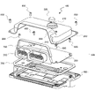
- FIG. 1 is an exploded perspective view showing one aspect of the electronic device 100.
- the electronic device 100 is, for example, an electronic control device including a microcomputer that controls an internal combustion engine, an automatic transmission, or the like mounted on an automobile.
- the electronic device 100 includes a cover 200, a substrate 300, and a base 400.
- the cover 200 and the base 400 are formed of a metal material having excellent thermal conductivity such as aluminum, and the cover 200 and the base 400 constitute a housing 500 for accommodating the substrate 300.
- the substrate 300 comprises a connector 310 and is fastened to the base 400 by a plurality of screws 600.
- the cover 200 and the base 400 are assembled with the waterproof sealing material 700 sandwiched between the joint surfaces, and are fastened by a plurality of screws 800.
- the cover 200 includes ventilation holes 210 that allow ventilation between the inside and the outside of the housing 500, and the ventilation holes 210 are equipped with a filter 220.
- the electronic device 100 has a heat radiating structure in which the heat of the heat generating element mounted on the substrate 300 is radiated through a heat radiating pedestal provided on the base 400, and heat that fills the gap between the heat generating element and the heat radiating pedestal.
- Thermal paste is used as the conductive material.
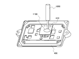
- FIG. 2 shows a step of applying thermal paste as a first step.
- the heat-dissipating grease 1100 is applied to the heat-dissipating pedestal 410 as a heat-dissipating member provided in a concave shape on the inner surface of the base 400 by using the coating nozzle 1000.
- the thermal paste 1100 is a thermal paste that is based on, for example, a grease such as modified silicone and is mixed with particles of a metal or metal oxide having high thermal conductivity, and is cured after assembly, that is, a curable thermal paste. Use grease.
- the heat radiating pedestal 410 is formed according to the position and shape of the heat generating element in order to dissipate the heat of the heat generating element mounted on the substrate 300 via the base 400.
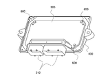
- FIG. 3 shows the outer shape of the microcomputer 320 as a heat generating element mounted on the substrate 300 and the base 400.
- a microcomputer 320 which is a rectangular heat generating element, is mounted on the surface of the substrate 300 facing the heat dissipation pedestal 410.
- the microcomputer 320 is, for example, a microcomputer that employs a BGA (Ball Grid Array) type package in which ball-shaped electrodes are arranged on a rectangular resin package. Further, a plurality of heat radiation fins 420 are integrally formed on the outer surface of the base 400.
- BGA Ball Grid Array
- FIG. 4 shows an assembling step of the substrate 300 as a second step.
- the substrate 300 is fastened to the base 400 to which the semi-liquid thermal paste 1100 is applied to the thermal pedestal 410 with screws 600.
- the thermal paste 1100 applied to the thermal pedestal 410 is sandwiched between the thermal pedestal 410 and the microcomputer 320 and spread out, and the gap between the thermal pedestal 410 and the microcomputer 320 is filled with the thermal paste 1100. ..
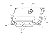
- FIG. 5 shows an assembly process of the base 400 and the cover 200 as a third process.
- the cover 200 is attached to the base 400 to which the substrate 300 is fastened by sandwiching the waterproof sealing material 700 on the joint surface, and the cover 200 is fastened by a plurality of screws 800 to assemble the electronic device 100.
- the thermal paste 1100 In the application of the thermal paste 1100 in the first step, it is difficult to control the coating weight of the thermal paste 1100 with high accuracy, and there is a concern that the thermal paste 1100 may protrude from the thermal paste pedestal 410 and adhere to the electrodes of the microcomputer 320. There is. If the thermal paste 1100 adheres to the electrode, the amount of distortion of the electrode increases, and the reliability of the electrical connection between the substrate 300 and the microcomputer 320 may decrease.
- the electronic device 100 has devised the shape of the heat radiating pedestal 410 as an adhesion measure for preventing the heat radiating grease 1100 from adhering to the electrodes of the microcomputer 320.
- 6-8 show the first aspect of the adhesion countermeasure.
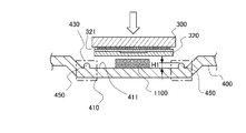
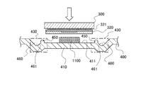
- FIG. 6 is a cross-sectional view of the heat radiating pedestal 410 and the board 300 in the process of assembling the substrate 300 to the base 400
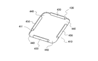
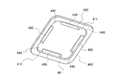
- FIG. 7 is a perspective view of the heat radiating pedestal 410
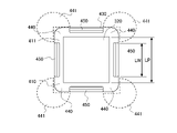
- FIG. 8 is a top view of the heat radiating pedestal 410.
- the area where the thermal paste 1100 is arranged is rectangular at a position outside the peripheral edge of the microcomputer 320 on the bottom surface 411 of the heat radiation pedestal 410 facing the microcomputer 320.
- the surrounding frame 430 was formed in the shape of a wall having a height H1 protruding from the bottom surface 411, and the upper part of the wall was cut off at the four corners of the frame 430 to make the height lower than H1 (specifically, the height is lower than H1.
- a notch 440 (with the wall removed) is formed.
- the structure is not limited to the structure in which the notches 440 are formed in all the four corners of the frame body 430, and the notches 440 can be formed in at least one of the four corners of the frame body 430.
- cutouts 440 may be formed at two diagonal corners of the four corners of the frame body 430, or cutouts 440 may be formed at two corners located at both ends of one side of the frame body 430.
- Notches 440 can be formed at three of the four corners of the frame body 430.
- the length LW of one side excluding the notch 440 of the frame body 430 is the length LP of one side of the package of the opposite microcomputer 320. I try to make it shorter than.
- a wall body 450 having a length LW shorter than the length LP of one side of the package of the opposite microcomputer 320 is placed at each position outside the four sides of the microcomputer 320 on the bottom surface 411 of the thermal pedestal 410. It is erected and four wall bodies 450 surround the area where the thermal paste 1100 is arranged in a rectangular shape.
- the notch 440 which is a portion where the wall body 450 is interrupted, functions as a relief opening that allows the outflow of the thermal paste 1100 from the inside of the frame body 430. Further, an accommodating portion 441 capable of accommodating the thermal paste 1100 flowing out from the region surrounded by the frame 430 is provided on the outside of the notch 440. In other words, a space is secured outside the notch 440 to allow the thermal paste 1100 flowing out of the notch 440 to flow in.
- the adhesion countermeasure when the thermal paste 1100 is expanded by the substrate 300, the expansion of the thermal paste 1100 from the center of the package of the microcomputer 320 toward the four sides is regulated by the wall 450 constituting the frame 430. Will be done.
- the excess thermal paste 1100 that is, the amount larger than the amount that fills the gap between the microcomputer 320 and the heat dissipation pedestal 410, is guided by the wall body 450 and flows toward the notches 440 at the four corners. It flows out from the notch 440 to the outside of the frame 430 and is accommodated in the accommodating portion 441.
- the excess thermal paste 1100 is cut out while keeping the thermal paste 1100 away from the electrode 321 of the microcomputer 320. Can be smoothly drained from.
- the thermal paste 1100 can be kept away from the electrode 321 of the microcomputer 320, so that the thermal paste 1100 is prevented from adhering to the electrode 321 of the microcomputer 320, and the electrical connection between the substrate 300 and the microcomputer 320 is performed. Reliability can be improved. Further, when the substrate 300 is fastened to the base 400 coated with the thermal paste 1100, the thermal paste 1100 can be spread substantially evenly around the base 400 to suppress the occurrence of bias in the thermal paste 1100, thus ensuring high heat dissipation. can.
- FIGS. 9 to 11 show a second aspect of adhesion countermeasures.
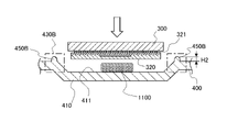
- 9 is a cross-sectional view of the heat dissipation pedestal 410 and the substrate 300 in the process of assembling the substrate 300 to the base 400
- FIG. 10 is a perspective view of the heat dissipation pedestal 410
- FIG. 11 is a top view of the heat dissipation pedestal 410.
- the thermal paste 1100 is arranged at a position outside the peripheral edge of the microcomputer 320, which is one step higher around the concave heat dissipation pedestal 410.
- the frame body 430B that surrounds the area in a rectangular shape is formed in the shape of a wall protruding at a height H2, and the upper part of the wall is cut off at the four corners of the frame body 430B to make the height lower than H2 (details).
- a notch 440B (with the wall removed) is formed.
- the length LW of one side excluding the notch 440B of the frame body 430B is the length LP of one side of the package of the opposite microcomputer 320. I try to make it shorter than. That is, in the second aspect, the wall body 450B having a length LW shorter than the length LP of one side of the package of the opposing microcomputer 320 is formed in a concave shape at a position outside the peripheral edge of the microcomputer 320.
- Each of the formed heat radiation pedestals 410 is erected on a higher portion around the heat radiation pedestal 410, and the four wall bodies 450B surround the arrangement area of the heat radiation grease 1100 in a rectangular shape.
- the notch 440B which is a portion where the wall body 450B is interrupted, functions as a relief opening that allows the outflow of the thermal paste 1100 from the inside of the frame body 430. Further, an accommodating portion 441B capable of accommodating the thermal paste 1100 flowing out from the region surrounded by the frame body 430B is provided outside the notch 440B. In other words, a space is secured outside the notch 440B to allow the thermal paste 1100 flowing out from the notch 440B to flow in.
- the second aspect of the adhesion countermeasure also suppresses the adhesion of the thermal paste 1100 to the electrode 321 of the microcomputer 320, and can improve the reliability of the electrical connection between the substrate 300 and the microcomputer 320. Further, when the substrate 300 is fastened to the base 400 coated with the thermal paste 1100, the thermal paste 1100 can be spread substantially evenly around the base 400 to suppress the occurrence of bias in the thermal paste 1100, thus ensuring high heat dissipation. can.
- FIG. 12-13 show a third aspect of adhesion countermeasures.
- FIG. 12 is a cross-sectional view of the heat radiating pedestal 410 and the board 300 in the process of assembling the substrate 300 to the base 400
- FIG. 13 is a perspective view of the heat radiating pedestal 410.
- the thermal paste is located outside the peripheral edge of the microcomputer 320 on the bottom surface 411 of the heat dissipation pedestal 410 facing the microcomputer 320, as in the first aspect.
- the frame body 430 that surrounds the filling area of 1100 in a rectangular shape is formed in the shape of a wall having a height H1 protruding from the bottom surface 411, and the upper part of the wall body is cut off at the four corners of the frame body 430 so that the height is higher than H1. Also formed a lowered notch 440.
- annular groove portion 460 surrounding the outside of the frame body 430 is formed, and the bottom surface 461 of the groove portion 460 is made lower than the bottom surface 411 of the heat dissipation pedestal 410.
- the groove portion 460 forms a pool portion on the outside of the notch 440 to store the thermal paste 1100 flowing out from the inside of the frame body 430.
- the thermal paste 1100 flowing out of the frame 430 through the notch 440 can be retained in the groove 460, and the thermal paste 1100 is attached to the electrode 321 of the microcomputer 320. It becomes possible to enhance the action of suppressing the adhesion.
- the heat generating element is not limited to the microcomputer, and the heat dissipation structure according to the present invention can also be applied to a heat generating element such as a power supply circuit.
- the annular groove portion 460 surrounding the outside of the frame body 430 is formed, but the recessed portions independently of each other are formed on the outside of the four notches 440, respectively, and the pool portion is formed.
- the thermal paste 1100 that has flowed out from the notch 440 can be flowed into the recessed portion and stored.
- a frame body 430 may be provided on the bottom surface 411 of the heat radiation pedestal 410 formed in a concave shape, and a frame body 430 may be provided on a higher portion around the heat radiation pedestal 410. can.
- thermal paste 1100 thermal paste that does not cure can be used.
- a through hole for communicating the inside and outside of the frame body 430 can be provided in the wall body 450.
- the structure is not limited to the structure in which the wall body 450 is provided linearly.
- the heat radiation grease 1100 is cut out 440 by forming the center of the wall body 450 so as to protrude toward the inside of the frame body 430. It is possible to improve the function of guiding toward.
Landscapes
- Engineering & Computer Science (AREA)
- Physics & Mathematics (AREA)
- Theoretical Computer Science (AREA)
- Human Computer Interaction (AREA)
- General Engineering & Computer Science (AREA)
- General Physics & Mathematics (AREA)
- Thermal Sciences (AREA)
- Microelectronics & Electronic Packaging (AREA)
- Cooling Or The Like Of Semiconductors Or Solid State Devices (AREA)
- Cooling Or The Like Of Electrical Apparatus (AREA)
Abstract
Description
なお、上記の放熱部材は、例えば、筐体に設けた放熱台座の部分である。
係る電子装置では、放熱グリスを放熱部材に塗布した後、発熱素子が実装された基板を放熱部材に組み付けることで、発熱素子と放熱部材との隙間を放熱グリスで埋める。
そして、発熱素子の領域からはみ出した放熱グリスが、発熱素子の電極に付着すると、電極の歪み量が増大し、基板と発熱素子との電気的接続の信頼性を低下させるおそれがあった。
また、本発明に係る電子装置の製造方法によれば、その一態様において、前記枠体で囲まれる前記放熱部材の部分に、半液状の前記熱伝導材を塗布する第1工程と、前記基板を前記放熱部材にねじによって締結し、前記放熱部材と前記発熱素子との間に挟まれる前記半液状の熱伝導材を押し広げる第2工程と、を有する。
図1は、電子装置100の一態様を示す分解斜視図である。
電子装置100は、例えば、自動車に搭載される内燃機関や自動変速機などを制御する、マイクロコンピュータを備えた電子制御装置である。
カバー200及びベース400は、アルミニウムなどの熱伝導性に優れた金属材料によって形成され、カバー200とベース400とは、基板300を収容する筐体500を構成する。
カバー200とベース400とは、防水シール材700を接合面に挟んで組み付けられ、複数のねじ800によって締結される。
カバー200は、筐体500の内部と外部との間での通気を可能にする通気孔210を備え、通気孔210にはフィルタ220が装着される。
後述するように、電子装置100は、基板300に実装された発熱素子の熱をベース400に設けた放熱台座を介して放熱する放熱構造を有し、発熱素子と放熱台座との隙間を埋める熱伝導材として放熱グリスを用いる。
第1工程では、ベース400の内側となる面に凹状に設けた、放熱部材としての放熱台座410に、塗布ノズル1000を用いて放熱グリス1100を塗布する。
なお、放熱台座410は、基板300に実装される発熱素子の熱を、ベース400を介して放熱させるために、発熱素子の位置及び形状に合わせて形成される。
基板300の放熱台座410と対向する面には、矩形の発熱素子であるマイクロコンピュータ320が実装される。
また、ベース400の外側の面には、複数の放熱フィン420が一体的に形成されている。
第2工程では、放熱台座410に半液状の放熱グリス1100を塗布したベース400に対し、ねじ600によって基板300を締結する。
ここで、放熱台座410に塗布された放熱グリス1100は、放熱台座410とマイクロコンピュータ320との間に挟まれて押し広げられ、放熱台座410とマイクロコンピュータ320との隙間が放熱グリス1100によって埋められる。
第3工程では、基板300が締結されたベース400に対し、接合面に防水シール材700を挟んでカバー200を組み付け、複数のねじ800によって締結することで、電子装置100を組み上げる。
そして、電極に放熱グリス1100が付着すると、電極の歪み量が増大し、基板300とマイクロコンピュータ320との電気的接続の信頼性を低下させるおそれがある。
図6-図8は、付着対策の第1態様を示す。
図6は基板300をベース400に組み付ける過程での放熱台座410及び基板300の断面図、図7は放熱台座410の斜視図、図8は放熱台座410の上面図である。
なお、枠体430の4隅の全てに切り欠き440を形成した構造に限定するものではなく、枠体430の4隅のうちの少なくとも1つに切り欠き440を形成することができる。
例えば、枠体430の4隅のうち1つの対角線上に位置する2隅に切り欠き440を形成したり、枠体430の1つの辺の両端に位置する2隅に切り欠き440を形成したり、枠体430の4隅のうちの3隅に切り欠き440を形成したりすることができる。
換言すれば、対向するマイクロコンピュータ320のパッケージの1辺の長さLPよりも短い長さLWの壁体450を、放熱台座410の底面411のマイクロコンピュータ320の4辺の外側となる位置それぞれに立設させ、4つの壁体450で、放熱グリス1100の配置領域を矩形に囲んでいる。
更に、切り欠き440の外側に、枠体430で囲まれる領域から流出した放熱グリス1100を収容可能な収容部441を設けてある。換言すれば、切り欠き440から流出する放熱グリス1100の流れ込みを許容する空間を、切り欠き440の外側に確保してある。
一方、余分な放熱グリス1100、つまり、マイクロコンピュータ320と放熱台座410との隙間を埋める量よりも多い分は、壁体450に案内されて4隅の切り欠き440に向けて流れ、4隅の切り欠き440から枠体430の外側に流出して収容部441に収容される。
ここで、壁体450の長さLWを、マイクロコンピュータ320のパッケージ長さLPよりも短くしたことで、マイクロコンピュータ320の電極321から放熱グリス1100を遠ざけながら、余分な放熱グリス1100を切り欠き440からスムースに流出させることができる。
また、放熱グリス1100を塗布したベース400に基板300を締結するときに、放熱グリス1100を周囲に略均等に広げて、放熱グリス1100に偏りが発生することを抑制できるため、高い放熱性を確保できる。
図9は基板300をベース400に組み付ける過程での放熱台座410及び基板300の断面図、図10は放熱台座410の斜視図、図11は放熱台座410の上面図である。
図9-図11に示した付着対策の第2態様では、マイクロコンピュータ320の周縁の外側となる位置であって、凹状に形成した放熱台座410の周囲の一段高い部分に、放熱グリス1100の配置領域を矩形に囲む枠体430Bを、高さH2で突出する壁状に形成し、また、枠体430Bの4隅に、壁の上部を切り取って高さをH2よりも低くした(詳細には、壁体を取り除いた)切り欠き440Bを形成してある。
つまり、第2態様においては、対向するマイクロコンピュータ320のパッケージの1辺の長さLPよりも短い長さLWの壁体450Bを、マイクロコンピュータ320の周縁の外側となる位置であって、凹状に形成した放熱台座410の周囲の一段高い部分にそれぞれ立設させ、4つの壁体450Bで、放熱グリス1100の配置領域を矩形に囲んでいる。
更に、切り欠き440Bの外側に、枠体430Bで囲まれる領域から流出した放熱グリス1100を収容可能な収容部441Bを設けてある。換言すれば、切り欠き440Bから流出する放熱グリス1100の流れ込みを許容する空間を、切り欠き440Bの外側に確保してある。
また、放熱グリス1100を塗布したベース400に基板300を締結するときに、放熱グリス1100を周囲に略均等に広げて、放熱グリス1100に偏りが発生することを抑制できるため、高い放熱性を確保できる。
図12は基板300をベース400に組み付ける過程での放熱台座410及び基板300の断面図、図13は放熱台座410の斜視図である。
図11-図12に示した付着対策の第3態様では、第1態様と同様に、マイクロコンピュータ320に対向する放熱台座410の底面411のマイクロコンピュータ320の周縁の外側となる位置に、放熱グリス1100の充填領域を矩形に囲む枠体430を、底面411から突出する高さH1の壁状に形成し、また、枠体430の4隅に、壁体の上部を切り取って高さをH1よりも低くした切り欠き440を形成した。
上記の溝部460は、切り欠き440の外側に、枠体430内から流出する放熱グリス1100を溜める溜まり部を形成する。
係る付着対策の第3態様によると、切り欠き440を介して枠体430の外部に流出した放熱グリス1100を、溝部460内に留め置くことができ、マイクロコンピュータ320の電極321に放熱グリス1100が付着することが抑止する作用をより高めることが可能になる。
また、好ましい実施形態を参照して本発明の内容を具体的に説明したが、本発明の基本的技術思想及び教示に基づいて、当業者であれば、種々の変形態様を採り得ることは自明である。
また、上記の付着対策の第3態様では、枠体430の外側を囲む環状の溝部460を形成したが、4個の切り欠き440の外側に相互に独立した凹陥部をそれぞれ形成し、溜まり部としての凹陥部に、切り欠き440から流出した放熱グリス1100を流入させて溜め置くことができる。
また、放熱グリス1100として、硬化しない放熱グリスを用いることができる。
また、壁体450を直線的に設ける構造に限定するものではなく、例えば、壁体450の中央が枠体430の内側に向けて迫り出した形状とすることで、放熱グリス1100を切り欠き440に向けて案内する機能を向上させることができる。
Claims (8)
- 電子装置であって、
矩形の発熱素子が実装された基板と、
前記発熱素子に対向する位置に配置された放熱部材と、
前記発熱素子と前記放熱部材との隙間を埋める熱伝導材と、
を有し、
前記放熱部材は、
前記発熱素子に対向する面の前記発熱素子の周縁の外側となる位置に、前記熱伝導材の配置領域を矩形に囲む枠体を備え、前記枠体の4隅のうちの少なくとも1つに切り欠きを形成した、
電子装置。 - 請求項1記載の電子装置であって、
前記枠体の前記切り欠きを除く1辺の長さが、対向する前記発熱素子の1辺の長さよりも短い、
電子装置。 - 請求項1記載の電子装置であって、
前記切り欠きの外側に、前記枠体で囲まれる領域よりも底面が低い、前記熱伝導材の溜まり部を設けた、
電子装置。 - 請求項3記載の電子装置であって、
前記溜まり部は、前記枠体の外側を囲む環状の溝である、
電子装置。 - 請求項1記載の電子装置であって、
前記放熱部材は、前記基板の筐体の一部をなし、前記発熱素子に対向する領域に形成された前記発熱素子の放熱台座を備え、
前記枠体は、前記放熱台座に備えられ、
前記放熱台座は、前記切り欠きの外側に、前記枠体で囲まれる領域から流出した前記熱伝導材を収容可能な収容部を有する、
電子装置。 - 請求項1記載の電子装置であって、
前記発熱素子は、BGAタイプのパッケージである、
電子装置。 - 請求項1記載の電子装置であって、
前記熱伝導材は、硬化型の放熱グリスである、
電子装置。 - 請求項1記載の電子装置を製造するための電子装置の製造方法であって、
前記枠体で囲まれる前記放熱部材の部分に、半液状の前記熱伝導材を塗布する第1工程と、
前記基板を前記放熱部材にねじによって締結し、前記放熱部材と前記発熱素子との間に挟まれる前記半液状の熱伝導材を押し広げる第2工程と、
を有する、電子装置の製造方法。
Priority Applications (4)
| Application Number | Priority Date | Filing Date | Title |
|---|---|---|---|
| DE112021005939.4T DE112021005939T5 (de) | 2020-11-13 | 2021-06-01 | Elektronische Vorrichtung und Verfahren zur Herstellung einer elektronischen Vorrichtung |
| JP2022561265A JP7441329B2 (ja) | 2020-11-13 | 2021-06-01 | 電子装置及び電子装置の製造方法 |
| CN202180052462.6A CN115989724A (zh) | 2020-11-13 | 2021-06-01 | 电子装置以及电子装置的制造方法 |
| US18/043,640 US12464681B2 (en) | 2020-11-13 | 2021-06-01 | Electronic device and electronic device manufacturing method |
Applications Claiming Priority (2)
| Application Number | Priority Date | Filing Date | Title |
|---|---|---|---|
| JP2020-189061 | 2020-11-13 | ||
| JP2020189061 | 2020-11-13 |
Publications (1)
| Publication Number | Publication Date |
|---|---|
| WO2022102149A1 true WO2022102149A1 (ja) | 2022-05-19 |
Family
ID=81600896
Family Applications (1)
| Application Number | Title | Priority Date | Filing Date |
|---|---|---|---|
| PCT/JP2021/020807 Ceased WO2022102149A1 (ja) | 2020-11-13 | 2021-06-01 | 電子装置及び電子装置の製造方法 |
Country Status (5)
| Country | Link |
|---|---|
| US (1) | US12464681B2 (ja) |
| JP (1) | JP7441329B2 (ja) |
| CN (1) | CN115989724A (ja) |
| DE (1) | DE112021005939T5 (ja) |
| WO (1) | WO2022102149A1 (ja) |
Citations (2)
| Publication number | Priority date | Publication date | Assignee | Title |
|---|---|---|---|---|
| JP2012015372A (ja) * | 2010-07-01 | 2012-01-19 | Nec Corp | 電子部品の冷却構造、電子部品装置、ヒートシンク |
| JP2017162860A (ja) * | 2016-03-07 | 2017-09-14 | 日立オートモティブシステムズ株式会社 | 電子制御装置 |
Family Cites Families (7)
| Publication number | Priority date | Publication date | Assignee | Title |
|---|---|---|---|---|
| US6785137B2 (en) * | 2002-07-26 | 2004-08-31 | Stmicroelectronics, Inc. | Method and system for removing heat from an active area of an integrated circuit device |
| JP4910439B2 (ja) * | 2006-03-23 | 2012-04-04 | 富士通セミコンダクター株式会社 | 半導体装置 |
| JP2008016653A (ja) * | 2006-07-06 | 2008-01-24 | Fujitsu Ltd | 半導体パッケージ、その製造方法、プリント基板及び電子機器 |
| JP5382049B2 (ja) * | 2010-06-30 | 2014-01-08 | 株式会社デンソー | 半導体装置 |
| US11387163B2 (en) * | 2018-03-30 | 2022-07-12 | Intel Corporation | Scalable debris-free socket loading mechanism |
| JP6650978B2 (ja) * | 2018-09-11 | 2020-02-19 | 日立オートモティブシステムズ株式会社 | 電子制御装置 |
| CN110867426A (zh) * | 2019-12-14 | 2020-03-06 | 周涛男 | 一种cpu顶盖 |
-
2021
- 2021-06-01 DE DE112021005939.4T patent/DE112021005939T5/de active Pending
- 2021-06-01 JP JP2022561265A patent/JP7441329B2/ja active Active
- 2021-06-01 CN CN202180052462.6A patent/CN115989724A/zh active Pending
- 2021-06-01 WO PCT/JP2021/020807 patent/WO2022102149A1/ja not_active Ceased
- 2021-06-01 US US18/043,640 patent/US12464681B2/en active Active
Patent Citations (2)
| Publication number | Priority date | Publication date | Assignee | Title |
|---|---|---|---|---|
| JP2012015372A (ja) * | 2010-07-01 | 2012-01-19 | Nec Corp | 電子部品の冷却構造、電子部品装置、ヒートシンク |
| JP2017162860A (ja) * | 2016-03-07 | 2017-09-14 | 日立オートモティブシステムズ株式会社 | 電子制御装置 |
Also Published As
| Publication number | Publication date |
|---|---|
| CN115989724A (zh) | 2023-04-18 |
| JPWO2022102149A1 (ja) | 2022-05-19 |
| DE112021005939T5 (de) | 2023-09-21 |
| US20230269913A1 (en) | 2023-08-24 |
| US12464681B2 (en) | 2025-11-04 |
| JP7441329B2 (ja) | 2024-02-29 |
Similar Documents
| Publication | Publication Date | Title |
|---|---|---|
| US6816377B2 (en) | Electronic control unit | |
| CA2273474C (en) | Electronic circuit device and method of fabricating the same | |
| JP3677403B2 (ja) | 発熱素子の放熱構造 | |
| JP4892527B2 (ja) | 電子制御装置 | |
| US20110235278A1 (en) | Circuit module | |
| JP4228753B2 (ja) | 電子制御装置 | |
| CN115244685B (zh) | 一种封装结构、电子设备及芯片封装方法 | |
| EP3883353B1 (en) | Automotive electronic device | |
| JP6945514B2 (ja) | 電子制御装置 | |
| WO2014208044A1 (ja) | 電子装置およびその電子装置の製造方法 | |
| KR20060051982A (ko) | 반도체 장치 및 전자기기 | |
| JP4910439B2 (ja) | 半導体装置 | |
| JP2014220278A (ja) | 半導体装置 | |
| JP2004072106A (ja) | 可調整ペデスタル熱界面 | |
| EP1178594A2 (en) | Electronic apparatus provided with an electronic circuit substrate | |
| JP2005012127A (ja) | 電子制御装置 | |
| JP7223639B2 (ja) | 電子制御装置 | |
| JP7661923B2 (ja) | 電子装置 | |
| JP7441329B2 (ja) | 電子装置及び電子装置の製造方法 | |
| JP2003224386A (ja) | 自動車用電子装置及び自動車用電子装置用ハウジング | |
| JP2017162860A (ja) | 電子制御装置 | |
| JPH11186766A (ja) | 半導体装置 | |
| JP2000252657A (ja) | 制御機器の放熱装置 | |
| JPWO2022102149A5 (ja) | ||
| JP2003023126A (ja) | 半導体装置 |
Legal Events
| Date | Code | Title | Description |
|---|---|---|---|
| 121 | Ep: the epo has been informed by wipo that ep was designated in this application |
Ref document number: 21891398 Country of ref document: EP Kind code of ref document: A1 |
|
| ENP | Entry into the national phase |
Ref document number: 2022561265 Country of ref document: JP Kind code of ref document: A |
|
| WWE | Wipo information: entry into national phase |
Ref document number: 112021005939 Country of ref document: DE |
|
| 122 | Ep: pct application non-entry in european phase |
Ref document number: 21891398 Country of ref document: EP Kind code of ref document: A1 |
|
| WWG | Wipo information: grant in national office |
Ref document number: 18043640 Country of ref document: US |